WO2024058254A1 - セラミックス焼結体基板、発光装置及びそれらの製造方法 - Google Patents
セラミックス焼結体基板、発光装置及びそれらの製造方法 Download PDFInfo
- Publication number
- WO2024058254A1 WO2024058254A1 PCT/JP2023/033612 JP2023033612W WO2024058254A1 WO 2024058254 A1 WO2024058254 A1 WO 2024058254A1 JP 2023033612 W JP2023033612 W JP 2023033612W WO 2024058254 A1 WO2024058254 A1 WO 2024058254A1
- Authority
- WO
- WIPO (PCT)
- Prior art keywords
- metal
- ceramic sintered
- substrate
- ceramic
- light emitting
- Prior art date
- Legal status (The legal status is an assumption and is not a legal conclusion. Google has not performed a legal analysis and makes no representation as to the accuracy of the status listed.)
- Ceased
Links
Images








Classifications
-
- H—ELECTRICITY
- H10—SEMICONDUCTOR DEVICES; ELECTRIC SOLID-STATE DEVICES NOT OTHERWISE PROVIDED FOR
- H10H—INORGANIC LIGHT-EMITTING SEMICONDUCTOR DEVICES HAVING POTENTIAL BARRIERS
- H10H20/00—Individual inorganic light-emitting semiconductor devices having potential barriers, e.g. light-emitting diodes [LED]
- H10H20/01—Manufacture or treatment
- H10H20/036—Manufacture or treatment of packages
-
- H—ELECTRICITY
- H10—SEMICONDUCTOR DEVICES; ELECTRIC SOLID-STATE DEVICES NOT OTHERWISE PROVIDED FOR
- H10H—INORGANIC LIGHT-EMITTING SEMICONDUCTOR DEVICES HAVING POTENTIAL BARRIERS
- H10H29/00—Integrated devices, or assemblies of multiple devices, comprising at least one light-emitting semiconductor element covered by group H10H20/00
- H10H29/80—Constructional details
- H10H29/85—Packages
- H10H29/8508—Package substrates, e.g. submounts
-
- H—ELECTRICITY
- H05—ELECTRIC TECHNIQUES NOT OTHERWISE PROVIDED FOR
- H05K—PRINTED CIRCUITS; CASINGS OR CONSTRUCTIONAL DETAILS OF ELECTRIC APPARATUS; MANUFACTURE OF ASSEMBLAGES OF ELECTRICAL COMPONENTS
- H05K1/00—Printed circuits
- H05K1/02—Details
- H05K1/03—Use of materials for the substrate
-
- H—ELECTRICITY
- H05—ELECTRIC TECHNIQUES NOT OTHERWISE PROVIDED FOR
- H05K—PRINTED CIRCUITS; CASINGS OR CONSTRUCTIONAL DETAILS OF ELECTRIC APPARATUS; MANUFACTURE OF ASSEMBLAGES OF ELECTRICAL COMPONENTS
- H05K1/00—Printed circuits
- H05K1/02—Details
- H05K1/11—Printed elements for providing electric connections to or between printed circuits
-
- H—ELECTRICITY
- H05—ELECTRIC TECHNIQUES NOT OTHERWISE PROVIDED FOR
- H05K—PRINTED CIRCUITS; CASINGS OR CONSTRUCTIONAL DETAILS OF ELECTRIC APPARATUS; MANUFACTURE OF ASSEMBLAGES OF ELECTRICAL COMPONENTS
- H05K3/00—Apparatus or processes for manufacturing printed circuits
- H05K3/10—Apparatus or processes for manufacturing printed circuits in which conductive material is applied to the insulating support in such a manner as to form the desired conductive pattern
- H05K3/12—Apparatus or processes for manufacturing printed circuits in which conductive material is applied to the insulating support in such a manner as to form the desired conductive pattern using thick film techniques, e.g. printing techniques to apply the conductive material or similar techniques for applying conductive paste or ink patterns
-
- H—ELECTRICITY
- H05—ELECTRIC TECHNIQUES NOT OTHERWISE PROVIDED FOR
- H05K—PRINTED CIRCUITS; CASINGS OR CONSTRUCTIONAL DETAILS OF ELECTRIC APPARATUS; MANUFACTURE OF ASSEMBLAGES OF ELECTRICAL COMPONENTS
- H05K3/00—Apparatus or processes for manufacturing printed circuits
- H05K3/40—Forming printed elements for providing electric connections to or between printed circuits
-
- H—ELECTRICITY
- H10—SEMICONDUCTOR DEVICES; ELECTRIC SOLID-STATE DEVICES NOT OTHERWISE PROVIDED FOR
- H10H—INORGANIC LIGHT-EMITTING SEMICONDUCTOR DEVICES HAVING POTENTIAL BARRIERS
- H10H20/00—Individual inorganic light-emitting semiconductor devices having potential barriers, e.g. light-emitting diodes [LED]
- H10H20/01—Manufacture or treatment
- H10H20/036—Manufacture or treatment of packages
- H10H20/0364—Manufacture or treatment of packages of interconnections
-
- H—ELECTRICITY
- H10—SEMICONDUCTOR DEVICES; ELECTRIC SOLID-STATE DEVICES NOT OTHERWISE PROVIDED FOR
- H10H—INORGANIC LIGHT-EMITTING SEMICONDUCTOR DEVICES HAVING POTENTIAL BARRIERS
- H10H20/00—Individual inorganic light-emitting semiconductor devices having potential barriers, e.g. light-emitting diodes [LED]
- H10H20/80—Constructional details
- H10H20/85—Packages
- H10H20/8508—Package substrates, e.g. submounts
-
- H—ELECTRICITY
- H10—SEMICONDUCTOR DEVICES; ELECTRIC SOLID-STATE DEVICES NOT OTHERWISE PROVIDED FOR
- H10H—INORGANIC LIGHT-EMITTING SEMICONDUCTOR DEVICES HAVING POTENTIAL BARRIERS
- H10H20/00—Individual inorganic light-emitting semiconductor devices having potential barriers, e.g. light-emitting diodes [LED]
- H10H20/80—Constructional details
- H10H20/85—Packages
- H10H20/857—Interconnections, e.g. lead-frames, bond wires or solder balls
-
- H—ELECTRICITY
- H10—SEMICONDUCTOR DEVICES; ELECTRIC SOLID-STATE DEVICES NOT OTHERWISE PROVIDED FOR
- H10H—INORGANIC LIGHT-EMITTING SEMICONDUCTOR DEVICES HAVING POTENTIAL BARRIERS
- H10H29/00—Integrated devices, or assemblies of multiple devices, comprising at least one light-emitting semiconductor element covered by group H10H20/00
- H10H29/01—Manufacture or treatment
- H10H29/036—Manufacture or treatment of packages
-
- H—ELECTRICITY
- H10—SEMICONDUCTOR DEVICES; ELECTRIC SOLID-STATE DEVICES NOT OTHERWISE PROVIDED FOR
- H10H—INORGANIC LIGHT-EMITTING SEMICONDUCTOR DEVICES HAVING POTENTIAL BARRIERS
- H10H29/00—Integrated devices, or assemblies of multiple devices, comprising at least one light-emitting semiconductor element covered by group H10H20/00
- H10H29/01—Manufacture or treatment
- H10H29/036—Manufacture or treatment of packages
- H10H29/0364—Manufacture or treatment of packages of interconnections
-
- H—ELECTRICITY
- H10—SEMICONDUCTOR DEVICES; ELECTRIC SOLID-STATE DEVICES NOT OTHERWISE PROVIDED FOR
- H10H—INORGANIC LIGHT-EMITTING SEMICONDUCTOR DEVICES HAVING POTENTIAL BARRIERS
- H10H29/00—Integrated devices, or assemblies of multiple devices, comprising at least one light-emitting semiconductor element covered by group H10H20/00
- H10H29/80—Constructional details
- H10H29/85—Packages
- H10H29/857—Interconnections
-
- H—ELECTRICITY
- H10—SEMICONDUCTOR DEVICES; ELECTRIC SOLID-STATE DEVICES NOT OTHERWISE PROVIDED FOR
- H10W—GENERIC PACKAGES, INTERCONNECTIONS, CONNECTORS OR OTHER CONSTRUCTIONAL DETAILS OF DEVICES COVERED BY CLASS H10
- H10W70/00—Package substrates; Interposers; Redistribution layers [RDL]
- H10W70/60—Insulating or insulated package substrates; Interposers; Redistribution layers
-
- H—ELECTRICITY
- H10—SEMICONDUCTOR DEVICES; ELECTRIC SOLID-STATE DEVICES NOT OTHERWISE PROVIDED FOR
- H10W—GENERIC PACKAGES, INTERCONNECTIONS, CONNECTORS OR OTHER CONSTRUCTIONAL DETAILS OF DEVICES COVERED BY CLASS H10
- H10W70/00—Package substrates; Interposers; Redistribution layers [RDL]
- H10W70/60—Insulating or insulated package substrates; Interposers; Redistribution layers
- H10W70/67—Insulating or insulated package substrates; Interposers; Redistribution layers characterised by their insulating layers or insulating parts
- H10W70/69—Insulating materials thereof
- H10W70/692—Ceramics or glasses
-
- H—ELECTRICITY
- H10—SEMICONDUCTOR DEVICES; ELECTRIC SOLID-STATE DEVICES NOT OTHERWISE PROVIDED FOR
- H10H—INORGANIC LIGHT-EMITTING SEMICONDUCTOR DEVICES HAVING POTENTIAL BARRIERS
- H10H29/00—Integrated devices, or assemblies of multiple devices, comprising at least one light-emitting semiconductor element covered by group H10H20/00
- H10H29/20—Assemblies of multiple devices comprising at least one light-emitting semiconductor device covered by group H10H20/00
- H10H29/24—Assemblies of multiple devices comprising at least one light-emitting semiconductor device covered by group H10H20/00 comprising multiple light-emitting semiconductor devices
Definitions
- the present disclosure relates to a ceramic sintered substrate, a light emitting device, and a manufacturing method thereof.
- via materials used for ceramic substrates include a through conductor whose main components are silver and copper. It is known that a non-eutectic region of silver and copper exists in the central region of the crystal.
- the via material used for ceramic substrates is filled with a first metal paste containing powder of a metal (B) having a melting point higher than that of the metal (A) with a melting point of 600°C or more and 1100°C or less and an active metal. It is known that a second metal paste containing powder of metal (A) is laminated at a position in contact with a first metal paste (for example, see Patent Documents 1 and 2).
- An object of the embodiments of the present disclosure is to provide a highly reliable ceramic sintered substrate, a light emitting device, and a method for manufacturing the same.
- a method for producing a ceramic sintered body substrate disclosed in the embodiment includes preparing a ceramic substrate in which a through hole is formed before firing, placing a first metal paste in the through hole, and disposing the first metal paste in the through hole.
- firing the ceramic substrate on which the metal paste is placed, and in placing the first metal paste the first metal paste includes a plurality of first metal powders and a plurality of active metal powders.
- the first metal powder includes a metal powder serving as a core, and a covering metal member having a melting point lower than that of the metal powder and covering at least a portion of the metal powder.
- the firing temperature is 700° C. or higher and lower than the melting point of the metal powder.
- the method for manufacturing a light emitting device disclosed in the embodiment includes preparing a ceramic sintered body substrate manufactured by the above-described method for manufacturing a ceramic sintered body substrate, and adding a light emitting element to the ceramic sintered body substrate.
- the first metal paste becomes a first metal body by firing, and in arranging the light emitting element, the first metal paste is placed in the through hole.
- the first metal body and the light emitting element are electrically connected directly or indirectly.
- the method for manufacturing a light emitting device disclosed in the embodiment includes preparing a ceramic sintered body substrate manufactured by the above-described method for manufacturing a ceramic sintered body substrate, and adding a light emitting element to the ceramic sintered body substrate.
- the first metal paste becomes a first metal body by firing
- the conductive paste becomes a conductor
- the light emitting element is arranged. In doing so, the first metal body or the conductor disposed in the through hole and the light emitting element are directly or indirectly electrically connected.
- the ceramic sintered body substrate disclosed in the embodiment includes a ceramic substrate having a through hole, and a first metal body disposed in the through hole, and the first metal body includes a plurality of
- the ceramic substrate includes a metal powder, a second metal, and a metal compound, the metal powder has a higher melting point than the second metal and is dispersed in the continuous second metal, and the ceramic substrate , having a reaction layer of the metal compound on the inner wall of the through hole, and having a reaction product of the metal compound at the grain boundary of the metal powder.
- the light emitting device disclosed in the embodiment includes the above-described ceramic sintered body substrate and a light emitting element electrically connected to the first metal body of the ceramic sintered body substrate.
- a highly reliable ceramic sintered body substrate, a light emitting device, and a manufacturing method thereof can be provided.
- FIG. 1 is a plan view schematically showing a ceramic sintered body substrate according to an embodiment.
- 2 is a cross-sectional perspective view schematically showing a cross section taken along line II-II in FIG. 1.
- FIG. FIG. 2 is an enlarged cross-sectional view schematically showing a state in which a first metal paste is placed in a through hole of a ceramic sintered body substrate according to an embodiment.
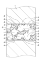
- FIG. 3B is an enlarged sectional view schematically showing a state of a first metal body obtained by sintering the ceramic sintered body substrate of FIG. 3A. It is a scanning electron micrograph showing an enlarged view of a first metal body disposed in a through hole of a ceramic sintered body substrate according to an embodiment.
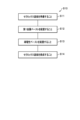
- FIG. 1 is a flowchart illustrating a method for manufacturing a ceramic sintered body substrate according to an embodiment.
- FIG. 2 is a cross-sectional view schematically showing a prepared ceramic substrate in a method for manufacturing a ceramic sintered body substrate according to an embodiment.
- FIG. 2 is a cross-sectional view schematically showing a state in which a first metal paste is placed in a through hole in a method for manufacturing a ceramic sintered body substrate according to an embodiment.
- FIG. 2 is a cross-sectional view schematically showing a state in which conductive paste is arranged in a method for manufacturing a ceramic sintered body substrate according to an embodiment.
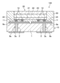
- 1 is a cross-sectional view illustrating a light-emitting device according to an embodiment of the present invention. 1 is a flowchart illustrating a method for manufacturing a light emitting device according to an embodiment.
- FIG. 2 is a cross-sectional view schematically showing a prepared ceramic sintered substrate in a method for manufacturing a light emitting device according to an embodiment.
- FIG. 2 is a cross-sectional view schematically showing a state in which a bonding member is placed on a ceramic sintered substrate in a method for manufacturing a light emitting device according to an embodiment.
- FIG. 2 is a cross-sectional view schematically showing a state in which light emitting elements are arranged in a method for manufacturing a light emitting device according to an embodiment.
- FIG. 2 is a cross-sectional view schematically showing a state in which a light reflecting member is arranged in a method for manufacturing a light emitting device according to an embodiment.
- FIG. 1 is a perspective view showing a light emitting device according to an embodiment as a light emitting module.
- 10A is a cross-sectional view schematically showing a cross section taken along the line XB-XB with a part of FIG. 10A omitted.
- FIG. 1 is a plan view schematically showing a ceramic sintered body substrate according to an embodiment
- FIG. 2 is a cross-sectional perspective view schematically showing a ceramic sintered body substrate according to an embodiment.
- FIG. 3A is an enlarged cross-sectional view schematically showing a state in which the first metal paste is placed in the through hole of the ceramic sintered substrate according to the embodiment.
- FIG. 3B is an enlarged sectional view schematically showing a state of a first metal body obtained by sintering the ceramic sintered body substrate of FIG. 3A.
- FIG. 4A is a scanning electron micrograph showing an enlarged view of the first metal body disposed in the through hole of the ceramic sintered body substrate according to the embodiment.
- FIG. 4B is a scanning electron micrograph showing an enlarged view of the first metal body disposed in the through hole of the ceramic sintered body substrate according to the embodiment.
- FIG. 7 is a cross-sectional view schematically showing a light emitting device according to an embodiment. Note that FIG. 3A shows a state before sintering the ceramic sintered body substrate. Further, FIG. 4A shows the state inside the through hole, and FIG. 4B shows the state near the interface between the through hole and the ceramic substrate 1.
- the ceramic sintered body substrate 10 includes a ceramic substrate 1 having a through hole 2 and a first metal body 3a disposed in the through hole 2, and the first metal body 3a includes a plurality of metal powders 4a. , a second metal 4b, and a metal compound 5.
- a plurality of metal powders 4a is used here, this does not mean that there are metal powders having a clear interface. This means that it is recognized that there are multiple aggregates of what appears to be metal powder based on the state of the ingredients. In other words, the metal powder is not completely melted and no interface exists.
- the metal powder 4a has the reactant 5b of the metal compound 5 on the surface and grain boundaries and is considered to be a single metal powder, even if a part of it is joined with other metal powders, It may be counted as one metal powder 4a.
- the metal powder 4a has a higher melting point than the second metal 4b, and is dispersed in the continuous second metal 4b.
- the ceramic substrate 1 has a reaction layer 5a of the metal compound 5 on the inner wall of the through hole 2, and a reaction material 5b of the metal compound 5 on the surface and grain boundaries of the metal powder 4a.
- the first metal body may be referred to as a first metal paste before firing
- the conductor may be referred to as a conductive paste before firing.
- the material after firing is different from the raw material, but for convenience of explanation, when expressing the product after firing, the name of the raw material is sometimes used.
- the ceramic substrate has different properties before and after firing, it will be explained as a ceramic substrate. Each structure of the ceramic sintered substrate 10 will be described below.
- the ceramic substrate 1 is a plate-shaped member that serves as the basis of the ceramic sintered body substrate 10.
- the shape of the ceramic substrate 1 in plan view is, for example, rectangular.
- the ceramic substrate 1 contains at least one selected from silicon nitride, aluminum nitride, and boron nitride.
- the ceramic substrate 1 is preferably made of nitride-based ceramics such as silicon nitride, aluminum nitride, and boron nitride, but oxide-based ceramics such as aluminum oxide, silicon oxide, calcium oxide, and magnesium oxide may also be used.
- the ceramic substrate 1 may also be made of silicon carbide, mullite, borosilicate glass, or the like.
- a through hole 2 is formed at a predetermined position in the thickness direction, and a first metal body 3a is arranged inside the through hole 2.
- the conductor 8a is arranged on the ceramic substrate 1 so that at least a portion of the first metal body 3a contacts the ceramic substrate 1. Note that the conductor 8a is arranged here so as to contact at least a portion of the first metal body 3a arranged in the through hole 2 on the front and back surfaces of the ceramic substrate 1.
- the conductor 8a is used as a wiring, a wiring pad, or an external connection electrode for electrically connecting the light emitting element 20.
- the through hole 2 of the ceramic substrate 1 is a via hole for electrically connecting the element electrode 24 of the light emitting element 20 to the outside of the ceramic substrate 1 via the first metal body 3a arranged inside.
- the through hole 2 may be formed by mechanical processing such as drilling or laser processing on a green sheet of a sintered ceramic substrate or an unfired ceramic substrate, or may be formed by etching or the like on the ceramic substrate 1 after sintering. Formed by chemical processing. It is preferable that the through hole 2 has a substantially circular or circular shape when cut in the horizontal direction with respect to the ceramic substrate 1.
- the diameter of the through hole 2 is preferably 0.05 mm or more and 0.5 mm or less. When the through hole 2 is 0.05 mm or more, it becomes easier to accurately arrange the first metal body 3a. Moreover, when the through-hole 2 is 0.5 mm or less, an appropriate filling amount can be achieved while maintaining high strength and low electrical resistance value.
- the first metal body 3a is arranged in the through hole 2 of the ceramic substrate 1.
- the first metal body 3a is a member that electrically connects to the light emitting element 20 either alone or together with the conductor 8a.
- the first metal body 3a includes, for example, a metal powder 4a, a second metal 4b, and a metal compound 5, and a reaction layer 5a of the metal compound 5 is formed on the inner surface defining the through hole 2.
- a reactant 5b of the metal compound 5 is formed on the surface or grain boundaries of the second metal 4b disposed around the metal powder 4a.
- the first metal paste 3 will be described here as containing an inorganic filler 7 excluding metal.
- the first metal powder including the metal powder 4a and the coated metal member 40b which becomes the second metal 4b is 63% by mass or more and 85% by mass or less, active
- the metal powder contains 1% by mass or more and 15% by mass or less, and the organic binder 6, which is a solvent, contains 5% by mass or more and 15% by mass or less.
- the first metal paste 3 becomes a first metal body after firing.
- the coated metal member 40b becomes the second metal 4b after firing.
- the active metal powder 50 becomes a metal compound 5 after firing.
- the first metal body 3a includes a metal powder 4a of 60% by mass or more and 80% by mass or less, a second metal 4b of 3% by mass or more and 25% by mass or less, and a reactant 5b of the metal compound 5 of 1% by mass or more and 15% by mass. Included below.
- a reaction layer 5a of the metal compound 5 is segregated on the inner surface defining the through hole 2. Note that in the first metal body 3a, the inorganic filler 7 is in a dispersed state.
- the metal powder 4a is a metal powder that becomes the core of the first metal powder 4 when placed as the first metal paste 3.
- the median diameter of the metal powder 4a is preferably 1 ⁇ m or more and 50 ⁇ m or less, more preferably 5 ⁇ m or more and 40 ⁇ m or less.
- the metal powder 4a has a diameter of 1 ⁇ m or more, it becomes easier to coat the second metal, which is the coated metal member 40b before firing. Further, when the metal powder 4a has a size of 50 ⁇ m or less, it becomes easier to arrange it in relation to the size of the through hole 2.
- the metal powder 4a is covered with a covering metal member 40b having a lower melting point than the metal powder 4a before sintering.
- the metal powder 4a is in a state of being dispersed together with the active metal powder 50, the organic binder 6, and the inorganic filler 7 in the first metal paste. After firing, the metal powder 4a becomes dispersed in the second metal 4b.
- the coated metal members 40b covering the metal powder 4a are melted by firing, and the coated metal members 40b cover each other and become partially continuous.
- the metal powder 4a is held in a dispersed state in this molten coated metal member 40b. This is because the metal powder 4a hardly sinks or floats because the molten coated metal member 40b has a small amount and high viscosity. Furthermore, the metal powder 4a maintains its particle size by being fired without melting.
- the metal powder 4a when the metal powder 4a is heated to a temperature higher than its melting point, it melts and becomes liquid; however, because the heating is performed at a temperature below the melting point of the metal powder 4a, the metal powder 4a itself does not melt and become liquid. . Since the metal powder 4a is not melted into a liquid state, no significant flow occurs in the first metal paste 3. This can reduce the possibility that the surface of the first metal paste 3 will shrink and become significantly concave. However, even if the metal powder 4a has a temperature below its melting point, a part of the surface of the metal powder 4a becomes softened due to the reaction with the coated metal member 40b, and other metal powders 4a and the second metal 4b placed in contact with or mixed with.
- the metal powder 4a and the second metal 4b there may be an interface between the metal powder 4a and the second metal 4b, but there may be no interface.
- the electrical resistance value can be lowered and the electrical conductivity and thermal conductivity can be increased.
- This metal powder 4a preferably contains at least one selected from Cu, Cr, and Ni, for example.
- the metal powder 4a also includes an alloy containing Cu, Cr, and Ni as main components. It is particularly preferable that the metal powder 4a is Cu or a Cu alloy.
- the melting point of the metal powder 4a is 1050°C or more and 2500°C or less. When the melting point of the metal powder 4a is 1050° C.
- the second metal 4b is placed at a position surrounding at least a portion or all of the metal powder 4a.
- the second metal 4b preferably has a lower melting point than the metal powder 4a, and includes, for example, at least one selected from Ag, Al, Zn, Sn, and an Ag-Cu alloy. In particular, Ag and Ag-Cu alloys are preferred. Since the melting point of Ag is 962° C. and the melting point of Ag-Cu alloy is around 780° C., the difference in melting point with the metal powder 4a can be reduced.
- the second metal 4b is arranged around the metal powder 4a so that it has a thickness of 3% or more and 30% or less with respect to the diameter or major axis of the metal powder 4a before melting, and is melted by firing. It is located around the metal powder 4a.
- the metal powders 4a are coated with a predetermined thickness, the metal powders 4a do not come into contact with each other more than necessary or separate from each other even after firing. By appropriately dispersing the metal powder 4a in this manner, it is possible to suppress unevenness of heat within the through hole.
- the melting point of the second metal 4b is preferably 200°C or more and 1000°C or less, more preferably 500°C or more and 980°C or less, and particularly preferably 750°C or more and 970°C or less. This is because if the melting point of the second metal 4b is 200° C. or higher, it can withstand reflow temperatures and the like when manufacturing a light emitting device.
- the melting point of the second metal 4b when the melting point of the second metal 4b is 1000° C. or less, it has a predetermined difference from the melting point of the metal powder 4a, so that the metal powder 4a does not melt and the dispersion state of the metal powder 4a is improved. can do. It is preferable that the difference in melting point between the second metal 4b and the metal powder 4a is at least 50°C or more, preferably 100°C or more.
- the second metal 4b is made of almost the same material as the coated metal member 40b, but since the thickness of the coated metal member 40b is extremely thin, the coated metal member 40b is heated at a firing temperature significantly lower than the melting point of the second metal 4b. It may also melt.
- the thickness of the covering metal member 40b of the second metal 4b before melting relative to the metal powder 4a is constant and covers the entire circumference. It is preferable that the coated metal member 40b has a thickness of 3% or more and 30% or less with respect to the diameter or major axis of the metal powder 4a. In addition, when the coated metal member 40b of the second metal 4b before melting covers a part of the metal powder 4a, the thinner part thereof is smaller than the diameter or major axis of the metal powder 4a. It is preferable that the thickness of the coating is 3% or more, and the thick part is 30% or less.
- a reactant 5b of the metal compound 5 is formed on the surface of the metal powder 4a or in the second metal 4b after firing.
- the case where the ceramic substrate 1 contains nitrogen is, for example, the case where at least one selected from silicon nitride, aluminum nitride, and boron nitride is used.
- the second metal 4b, together with the components of the metal compound 5 forms a reaction layer 5a of the metal compound 5 on the inner surface defining the through hole 2.
- the metal compound 5 may be placed between the metal powders 4a. At least a portion or all of the active metal powder 50 becomes the metal compound 5 by firing.
- the active metal powder 50 is dispersed in the first metal paste 3, and the fired metal compound 5 is also dispersed in the first metal body 3a.
- the active metal powder 50 will be explained using titanium hydride (TiH 2 ) as an example. Titanium hydride releases hydrogen by firing to become metallic titanium, and then the titanium is oxidized or nitrided to become titanium oxide, titanium nitride, or the like.
- the active metal powder 50 contained in the first metal paste 3 reacts with the nitrogen in the ceramic substrate 1, and at the interface between the first metal paste 3 and the ceramic substrate 1, metal A reaction layer 5a of compound 5 is formed. Further, the reactant 5b of the metal compound 5 is arranged so that the space between the metal powders 4a is continuous or arranged at a grain boundary.
- the metal compound 5 is placed in direct contact with the metal powder 4a, in contact with or surrounding the second metal 4b, or in a state surrounding the inorganic filler 7. As described above, the metal compound 5, together with the components of the second metal 4b, forms a reaction layer 5a on a part or all of the inner surface that partitions the through hole 2, and connects the first metal body 3a and the ceramic substrate. This improves the adhesion strength with 1.
- the melting points of the second metal 4b and the metal compound 5 are lower than the melting point of the metal powder 4a. Therefore, even if the metal powder 4a is fired while being placed in the through hole 2 as the first metal paste 3, and the coated metal member 40b is melted and the active metal powder 50 reacts, the metal powder 4a is 4a remains dispersed. Further, the second metal 4b melted from the coated metal member 40b is continuously arranged within the through hole 2.
- the coated metal member 40b so as to cover the metal powder 4a and firing it at a predetermined firing temperature, the coated metal member It is possible to reduce the flow caused by the melting of 40b, and to arrange it in a dispersed manner without being unevenly distributed from the upper end to the lower end in the through hole 2.
- a reactant 5b of the metal compound 5 reacted from the active metal powder 50 is dispersed in the first metal body 3a, and a reaction layer 5a is arranged on the inner surface defining the through hole 2. Even if there is a difference in specific gravity between the metal powder 4a, the second metal 4b, and the metal compound 5, a dispersed state can be maintained without settling or floating.
- the active metal powder 50 is preferably one or more materials selected from, for example, TiH 2 , CeH 2 , ZrH 2 , LaH 2 , and MgH 2 .
- the active metal powder 50 By firing this active metal powder 50, all or part of the hydrogen is desorbed and reacts with nitrogen, oxygen, carbon, etc. contained in the ceramic substrate 1, inorganic filler 7, etc. to form metal nitrides and metal oxides. , changes into carbide metals, etc.
- This changed substance is a metal compound.
- TiH 2 as the active metal powder 50, and by containing TiH 2 , it reacts with nitrogen contained in the ceramic substrate 1 etc., and at the interface with the ceramic sintered body substrate 10, TiH 2 A reaction layer 5a like this is formed.
- the adhesion between the first metal body 3a which is a conductive via, and the ceramic substrate 1 is improved, and the first metal body 3a is firmly adhered to the through hole 2.
- the inorganic filler 7 is dispersed within the first metal paste 3 to reduce the occurrence of cracks.
- the inorganic filler 7 include ceramic filler, metal filler, and glass filler.
- the inorganic filler 7 may be aluminum oxide, silicon oxide, or the like.
- the inorganic filler 7 is contained in a content range that does not interfere with the effects of other ingredients.
- the organic binder 6 is a member contained in the first metal paste 3 before firing. After firing, the organic binder 6 evaporates and does not remain in the first metal paste 3.
- the organic binder 6 may be, for example, a solvent or resin material that is generally used as a via material.
- the conductor 8a is a conductive member that forms wiring of a preset wiring pattern, wiring pads, external connection electrodes, and the like.
- the conductor 8a may be formed by firing the conductive paste 8.
- the conductive paste 8 is arranged so as to be in contact with at least a portion of the first metal paste 3 or the first metal body 3a.
- the thickness of the conductive paste 8 is preferably, for example, 12 ⁇ m or more and 35 ⁇ m or less.
- the wiring or connection pad of the conductive paste 8 can be formed by, for example, etching or printing.
- the conductive paste 8 is arranged as a wiring or the like on the first surface of the ceramic substrate 1, and is also arranged as a wiring or the like on the second surface opposite to the first surface.
- the shape of the conductive paste 8 is rectangular, circular, linear, etc. in plan view, and is arranged on the first surface of the ceramic substrate 1 at a distance from each other, and on the second surface at a distance from each other. There is.
- the conductive paste 8 is arranged in such a way that the size of the conductive paste 8 is set on the first surface and the second surface of the ceramic substrate 1, for example, so that the area on the side disposed on the first surface is larger. , is different from the second surface side, but may be the same size.
- the conductive paste 8 is illustrated as a rectangle so as to be in contact with the entire circular first metal paste when viewed from above, but its shape and arrangement are arbitrary and are not limited.
- this conductive paste 8 uses the same member as the first metal paste 3, for example.
- the material of the conductor 8a copper foil may be used as a metal member.
- the material of the conductive paste 8 may be, for example, a single substance such as gold, silver, copper, platinum, or aluminum, or an alloy thereof, or a mixture of mixed powder and a resin binder.
- the resin binder for example, thermosetting resin such as epoxy resin or silicone resin can be used.
- the conductive paste 8 contains a reducing agent such as an organic acid. Thereby, the electrical resistance in connection with the light emitting element 20 can be reduced.
- the ceramic sintered body substrate 10 having the above configuration has high reliability because the first metal paste 3 is firmly bonded to the inner surface that defines the through hole 2 of the ceramic substrate 1, and the distance between the ceramic substrate 10 and the light emitting element is high. electrical connection can be ensured.
- the number of through holes 2 in the ceramic substrate 1 may be two or more, and the shape thereof is not limited to a circle, such as an ellipse or a rectangle.
- the shape of the conductor 8a may be square, rectangular, or trapezoidal, or may include a curved portion.
- the light emitting element 20 may be directly connected to a part of the first metal body 3a without providing the conductor 8a.
- FIG. 5 is a flowchart illustrating a method for manufacturing a ceramic sintered body substrate according to an embodiment.
- FIG. 6A is a cross-sectional view schematically showing a prepared ceramic substrate in the method for manufacturing a ceramic sintered body substrate according to the embodiment.
- FIG. 6B is a cross-sectional view schematically showing a state in which the first metal paste is placed in the through hole in the method for manufacturing a ceramic sintered body substrate according to the embodiment.
- FIG. 6C is a cross-sectional view schematically showing a state in which conductive paste is arranged in the method for manufacturing a ceramic sintered body substrate according to the embodiment.
- a method for manufacturing a ceramic sintered substrate S10 includes preparing a ceramic substrate in which a through hole is formed before firing S11, disposing a first metal paste in the through hole S12, and disposing the first metal paste.
- S14 includes firing the ceramic substrate.
- the first metal paste includes a plurality of first metal powders and a plurality of active metal powders, and the first metal powder is a core metal. It has a powder and a covering metal member that has a melting point lower than that of the metal powder and covers at least a portion of the metal powder.
- the firing temperature is 700° C. or higher and lower than the melting point of the metal powder.
- the method S10 for manufacturing a ceramic sintered body substrate for example, after disposing the first metal paste S12 and before firing the ceramic substrate S14, at least a portion of the ceramic substrate is mixed with the first metal paste.
- S13 is performed in which a conductive paste is placed on the ceramic substrate so as to be in contact with the ceramic substrate.
- a ceramic substrate S11 (hereinafter referred to as step S11), for example, a flat substrate is prepared.
- the prepared ceramic substrate 1 has a number of through holes 2 formed therein by laser machining or the like to correspond to connection portions of device electrodes 24 and the like of the light emitting device 20, which will be described later.
- the through holes 2 are formed at two locations, for example.
- the ceramic substrate 1 may be prepared with a number of through holes 2 formed therein corresponding to the size of the area on which the plurality of light emitting elements 20 are arranged and the number of element electrodes 24, or with a predetermined number of through holes 2 formed therein. It may be prepared by cutting it into a size in which the light emitting element 20 is arranged.
- step S12 Placing the first metal paste S12 (hereinafter referred to as step S12) is to place the first metal paste in the through hole 2 formed in the ceramic substrate 1.
- the first metal paste 3 is placed in the through hole 2 by, for example, screen printing or injection using a nozzle.
- the first metal powder 4 includes a metal powder 4a serving as a core, and a covering metal member 40b that covers the metal powder 4a.
- step S12 when placing the first metal paste 3 in the through hole 2, the first metal paste 3 is applied from the first surface, which is one surface of the ceramic substrate 1, using a squeegee, which is a tool used for screen printing, for example. It is preferable to place the paste in the through-holes 2, and then place the first metal paste in the through-holes 2 from the second surface, which is the other surface of the ceramic substrate 1, using a squeegee in the same manner as the first surface.
- step S13 disposing the conductive paste 8 S13 (hereinafter referred to as step S13) is performed.
- the conductive paste 8 is placed on the ceramic substrate 1 so that it is at least partially in contact with the first metal paste 3 placed in the through hole 2.
- the conductive paste 8 is placed so as to be in contact with the entire surface of the first metal paste 3 exposed from the through hole 2 of the ceramic substrate 1.
- the conductive paste 8 is arranged in a rectangular shape at two locations on the first surface of the ceramic substrate 1 and two locations on the second surface of the ceramic substrate 1, a total of four locations.
- the conductive paste 8 is used to form rectangular wiring or wiring pads on the first and second surfaces of the ceramic substrate 1 through a mask by screen printing, metal mask printing, or the like.
- the first metal paste 3 and the conductive paste 8 used in Step S12 and Step S13 have fluidity, and can be freely arranged in the through hole 2 of any shape, and can be arranged in any shape, It can be placed by applying a thick layer and then curing it.
- step S14 the ceramic substrate is fired in step S14 (hereinafter referred to as step S14).
- the firing temperature is 700° C. or higher and lower than the melting point of the metal powder.
- the firing atmosphere is preferably an Ar atmosphere of 99.9% or more or a vacuum atmosphere of 10 ⁇ 5 Pa or less.
- the firing temperature is preferably 700°C or more and 1000°C or less, more preferably 700°C or more and 980°C or less, and particularly preferably 750°C or more and 970°C or less.
- the ceramic sintered body substrate 10 can be manufactured by step 14. As shown in FIGS. 3B and 4, when the state of the first metal paste 3 is observed after firing, it is found that, for example, the copper powder that is the metal powder 4a is the same as the continuous Ag powder that is the second metal 4b. -The dispersed state in the Cu alloy is maintained in the same manner as before firing. This is because the firing temperature is adjusted to be below the predetermined temperature as described above, so that the metal powder 4a does not melt, and the coated metal member 40b melts into the second metal 4b and active metal powder. This is because the metal compound 5 with which 50 has reacted is placed between the metal powders 4a.
- the active metal powder 50 reacts with the metal compound 5 to form a reactant 5b of the metal compound 5 on the surface of the coated metal member 40b before melting, and at the same time defines the through hole 2 of the ceramic substrate 1.
- a reaction layer 5a of metal compound 5 is formed on the inner surface.
- the reaction layer 5a of the metal compound 5 is formed by the first metal paste 3 after firing, so that the first metal paste 3 is strongly bonded to the through hole 2. Therefore, the ceramic sintered substrate 10 has stable conductivity because the metal powder 4a is dispersed relatively evenly in the electrical connection made through the first metal body 3a. Further, since the reaction layer 5a of the metal compound 5 is formed, the bonding strength between the first metal paste and the inner surface defining the through hole 2 is high, and a highly reliable configuration can be realized.
- the light-emitting device 100 is a device that emits light by disposing a light-emitting element 20 on a ceramic sintered substrate 10, and although the number of light-emitting elements 20 is one in the drawing, the number of light-emitting elements 20 may be plural.
- the arrangement is not particularly limited, and may be arranged in a line.
- the light emitting device 100 includes the ceramic sintered substrate 10 described above and the light emitting element 20 electrically connected to the conductor 8a that serves as the wiring of the ceramic sintered substrate 10.
- the light-emitting device 100 includes, as an example, a light-reflecting member 30 that covers the side surface of the light-emitting element 20 and the top of the ceramic sintered body substrate 10.
- wiring patterns can be formed in various patterns depending on the application.
- the light emitting element 20 includes a pair of element electrodes 24, a translucent member 23 disposed on the light extraction surface side of the light emitting element 20, an element substrate 22, and a semiconductor stack 21.
- the light emitting element 20 has a semiconductor laminate 21 on an element substrate 22.
- a light-transmitting member 23 is arranged on the upper surface side of the element substrate 22, which is a light extraction surface, and A semiconductor stacked body 21 is provided on one side, and a pair of element electrodes 24 are provided on the semiconductor stacked body 21 side.
- any composition can be used for the semiconductor stack 21 depending on the desired emission wavelength , but for example, a nitride semiconductor (In , 0 ⁇ X, 0 ⁇ Y, X+Y ⁇ 1), GaP, or GaAlAs or AlInGaP, which can emit red light, can be used. Further, the size and shape of the light emitting element 20 can be selected as appropriate depending on the purpose of use.
- a sapphire substrate or a silicon substrate is used, for example.
- the translucent member 23 is made of, for example, a translucent resin material, and can be made of epoxy resin, silicone resin, or a mixture of these resins.
- the translucent member 23 may contain a phosphor, for example, by including a phosphor that absorbs blue light from the light emitting element 20 and emits yellow light, it can emit white light. Can be done. Further, the translucent member 23 may contain multiple types of phosphors, for example, a phosphor that absorbs blue light from the semiconductor laminate 21 and emits green light, and a phosphor that emits red light. White light can also be emitted from the light emitting element 20 by including a phosphor that emits .
- phosphors examples include yttrium-aluminum-garnet-based phosphors (e.g., Y 3 (Al, Ga) 5 O 12 :Ce), lutetium-aluminum-garnet-based phosphors (e.g., Lu 3 (Al , Ga) 5 O 12 :Ce), terbium-aluminum-garnet phosphor (e.g., Tb 3 (Al, Ga) 5 O 12 :Ce), ⁇ -sialon phosphor (e.g., (Si, Al) 3 (O , N) 4 :Eu), ⁇ -sialon phosphor (for example, Mz(Si,Al) 12 (O,N) 16 (where 0 ⁇ z ⁇ 2, and M is Li, Mg, Ca, Y, and (lanthanide elements excluding La and Ce)), nitride-based phosphors such as CASN-based phosphors (e.g., CA
- Phosphor e.g. K 2 SiF 6 :Mn
- KSAF phosphor e.g. K 2 (Si,Al)F 6 :Mn
- MGF phosphor e.g. 3.5MgO ⁇ 0.5MgF 2 ⁇ Fluoride-based phosphors such as GeO 2 :Mn
- quantum dot phosphors such as perovskite and chalcopyrite, etc.
- the element electrode 24 is connected to the conductor 8a of the ceramic sintered substrate 10 by the metal bump 12 via the bonding member 11.
- the conductor 8a is preferably subjected to surface treatment such as plating in which Ni/Pd/Au are laminated in this order.
- One of the element electrodes 24 is a p-electrode, and the element electrode 24 is arranged at a distance from the other n-electrode so as not to be electrically short-circuited.
- the element electrode 24 has a configuration in which a p electrode and an n electrode are disposed at one location each, but it may also be configured such that either one is disposed at two locations and the other is disposed at one location.
- the metal bump 12 electrically connects the element electrode 24 and the conductor 8a.
- the metal bump 12 may be placed on the element electrode 24 side or on the conductor 8a side. Further, the shape, size, and number of the metal bumps 12 can be set as appropriate as long as they can be arranged within the range of the element electrodes 24. Further, the size of the metal bump 12 can be adjusted as appropriate depending on the size of the semiconductor stack, the required light emitting output of the light emitting element, etc. It will be done.
- the metal bump 12 can be formed of, for example, Au, Ag, Cu, Al, Sn, Pt, Zn, Ni, or an alloy thereof, and can be formed of, for example, a stud bump known in the art.
- the stud bump can be formed using a stud bump bonder, a wire bonding device, or the like. Further, the metal bumps 12 may be formed by methods known in the art, such as electrolytic plating, electroless plating, vapor deposition, and sputtering.
- the joining member 11 used here includes, for example, tin-bismuth-based, tin-copper-based, tin-silver-based, gold-tin-based solder, alloys containing Au and Sn as main components, and solders containing Au and Si as main components.
- eutectic alloys such as alloys whose main components are Au and Ge, paste materials such as silver, gold, palladium, anisotropic conductive materials such as ACP and ACF, and low melting point metals. Examples include brazing filler metals, conductive adhesives that are combinations of these materials, conductive composite adhesives, and the like.
- the light reflecting member 30 is a member having light reflecting properties.
- the light reflecting member 30 is arranged to cover the first surface of the ceramic sintered substrate 10 and to cover the side surface of the light emitting element 20 . Further, the light reflecting member 30 is arranged so as to expose the light extraction surface of the light emitting element 20, and is arranged so as to be flush with the light transmitting member 23 of the light emitting element 20. Note that, as an example, the light reflecting member 30 is also arranged between the lower surface of the light emitting element 20 and the first surface of the ceramic sintered body substrate 10.
- the light reflecting member 30 has high reflectance in order to effectively utilize the light from the light emitting element 20. It is preferable that the light reflecting member 30 is white.
- the reflectance of the light reflecting member 30 is preferably, for example, 90% or more, and more preferably 94% or more, at the wavelength of the light emitted by the light emitting element 20.
- the light reflecting member 30 is made of, for example, thermoplastic resin such as acrylic resin, polycarbonate resin, cyclic polyolefin resin, polyethylene terephthalate resin, polyethylene naphthalate resin, or polyester resin, or thermosetting resin such as epoxy resin or silicone resin. Polymer resins can be used. Further, as the light diffusing material, for example, known materials such as titanium oxide, silica, alumina, zinc oxide, or glass can be used.
- the light emitting device 100 having the above configuration includes the first metal body 3a in the ceramic sintered body substrate 10, so that the bonding strength between the first metal body 3a and the ceramic substrate 1 is high and reliability is improved. be able to.
- the light emitting device 100 uses one light emitting element 20 as one unit to control brightness and turning on and off, but the number of light emitting elements 20 included in one unit may be one. There may be more than one. For example, four light emitting elements 20 arranged in 1 row and 4 columns, 2 rows and 2 columns, or 9 light emitting elements 20 arranged in 3 rows and 3 columns can be made into one unit.
- FIG. 8 is a flowchart illustrating a method for manufacturing a light emitting device according to an embodiment.
- FIG. 9A is a cross-sectional view schematically showing a prepared ceramic sintered body substrate in the method for manufacturing a light emitting device according to the embodiment.
- FIG. 9B is a cross-sectional view schematically showing a state in which convenient members are arranged on a ceramic sintered body substrate.
- FIG. 9C is a cross-sectional view schematically showing a state in which light emitting elements are arranged in the method for manufacturing a light emitting device according to the embodiment.
- FIG. 9D is a cross-sectional view schematically showing a state in which a light reflecting member is arranged in the method for manufacturing a light emitting device according to the embodiment.
- the manufacturing method S20 of a light emitting device includes preparing a ceramic sintered body substrate manufactured by the ceramic sintered body substrate manufacturing method S10 described above, S21, and arranging a light emitting element on the ceramic sintered body substrate S22. , and in arranging the light emitting element S22, the first metal member disposed in the through hole and the light emitting element are directly or indirectly electrically connected. Note that, after arranging the light emitting elements in S22, arranging a light reflecting member in S23 may be included. Further, in arranging the light emitting element S22, the element electrode 24 may be directly or indirectly connected to the conductor 8a that is in contact with at least a portion of the first metal body 3a.
- Preparing a ceramic sintered body substrate S21 (hereinafter referred to as step S21) is to prepare the ceramic sintered body substrate 10 manufactured by the ceramic sintered body substrate manufacturing method S10 described above.
- the ceramic sintered body substrate 10 has four conductive bodies 8a connected to the first metal bodies 3a disposed in the through holes 2 on the first and second surfaces thereof. Note that the shape, size, and spacing of the conductor 8a can be adjusted to match the element electrode 24 of the light emitting element 20.
- the ceramic sintered substrate 10 has a plurality of areas in which the light emitting elements 20 are arranged, and after arranging the light reflecting member 30 described later, it may be made into a size for each light emitting device 100, or one light emitting element 20 may be arranged. The size may be set for each device 100.
- step S22 means placing the light emitting element 20 on the ceramic sintered substrate 10.
- the element electrodes 24 of the light emitting elements 20 are connected using the metal bumps 12 via the bonding members 11 arranged on the conductor 8a.
- the conductive bonding member 11 is, for example, a bump made of gold, silver, copper, etc., a conductive paste material that is a mixture of metal powder such as gold, silver, copper, platinum, aluminum, etc., and a resin binder, or, A tin-silver-copper (SAC)-based solder or a tin-bismuth (SnBi)-based solder can be used.
- SAC tin-silver-copper
- SnBi tin-bismuth
- Arranging the light reflecting member S23 means arranging the light reflecting member 30 so as to cover the first surface, which is the upper surface of the ceramic sintered body substrate 10, and to cover the side surface of the light emitting element 20. It is to be.
- the light reflecting member 30 is placed on the ceramic sintered substrate 10 so as to expose the upper surface of the translucent member 23 that surrounds the light emitting element 20 and serves as a light extraction surface of the light emitting element 20.
- the light reflecting member 30 is arranged to have a rectangular shape in plan view.
- a singulation work is performed as necessary.
- one unit of the light emitting device 100 is set in advance by the number of light emitting elements 20 used. Therefore, when a plurality of light emitting devices 100 are manufactured at once, a singulation operation is performed.
- a plurality of light emitting devices 100 are manufactured by cutting into a grid pattern. Further, as a cutting method, for example, a disc-shaped rotary blade, an ultrasonic cutter, laser beam irradiation, a blade, etc. can be used.
- the method S20 for manufacturing a light emitting device having the above configuration is performed by improving the bonding strength of the first metal paste 3 placed in the through hole 2 of the ceramic substrate 1 by the method S10 for manufacturing a sintered ceramic substrate. It becomes possible to improve reliability and to stably control the light emitting element 20.
- a light emitting module 100A may include a plurality of light emitting devices 100 in a row (11 pieces in the drawing). The configuration of the light emitting module 100A will be described.
- FIG. 10A is a perspective view showing an application example of the light emitting device.
- FIG. 10B is a sectional view showing a cross section with a part of FIG. 10A omitted.
- the light emitting module 100A includes 11 light emitting devices 100 in a row, has a frame 140 outside the light reflecting member 30, and has a module substrate 150 connected to the conductor 8a below the ceramic sintered substrate 10. There is.
- the frame body 140 is a member for surrounding the light reflecting member 30 that covers the plurality of light emitting devices 100.
- the frame 140 is formed in a rectangular annular shape, for example, in a plan view, and is disposed so as to surround the light reflecting member 30 .
- the frame 140 can be formed using a frame-shaped member made of metal, alloy, or ceramic.
- the metal include Fe, Cu, Ni, Al, Ag, Au, Al, Pt, Ti, W, and Pd.
- the alloy include alloys containing at least one of Fe, Cu, Ni, Al, Ag, Au, Al, Pt, Ti, W, Pd, and the like.
- a resin material may be used as the frame 140.
- the metal, alloy, or ceramic member may be embedded in the frame 140 made of a resin material, or a part of the frame 140 may be made of a resin material, and the other part may be made of a metal, alloy, or ceramic member. It may be formed by
- the module board 150 is a member on which the light emitting device 100 is placed, and is used to electrically connect the light emitting device 100 to the outside.
- the module substrate 150 is, for example, formed into a substantially rectangular shape when viewed from above.
- Module board 150 includes a board section 160 and a wiring board section 170.
- As the material of the substrate portion 160 for example, it is preferable to use an insulating material, and it is also preferable to use a material that hardly transmits the light emitted from the light emitting element 20, external light, etc.
- ceramics such as alumina, aluminum nitride, mullite, polyamide, polyphthalamide, polyphenylene sulfide, thermoplastic resins such as liquid crystal polymers, epoxy resins, silicone resins, modified epoxy resins, urethane resins, phenolic resins, etc. resin can be used. Among these, it is preferable to use ceramics, which have excellent heat dissipation properties.
- the wiring board section 170 is formed on the substrate section 160 at a position facing the conductor 8a below the light emitting device 100.
- the material for the wiring board portion 170 include those exemplified as the materials used for the first metal body 3a, the conductor 8a, and the like.
- the module board 150 is bonded to the frame 140 via a conductive adhesive 151, and is arranged such that the conductor 8a and the wiring board portion 170 are bonded to each other.
- the conductive adhesive 151 for example, eutectic solder, conductive paste, bumps, etc. may be used.
- a protection element 125 is arranged on the ceramic sintered body substrate 10 in parallel with each light emitting element 20.
- the light emitting module 100A is configured as described above, when it is driven, the following occurs. That is, in the light emitting module 100A, current is supplied to the light emitting element 20 from an external power source via the wiring board section 170, the conductive paste, the first metal paste, and the element electrode 24, and the light emitting element 20 emits light. The light emitted by the light emitting element 20 that travels upward is extracted to the outside above the light emitting device 100 via the light transmitting member 23 . Further, the light traveling downward is reflected by the ceramic sintered substrate 10 and taken out to the outside of the light emitting device 100 via the light-transmitting member 23.
- the configuration of the optical system can be made simple and compact. be able to.
- the light emitting devices 100 are arranged on a sheet member, the frame body 140 is arranged around it, and in this state, the light reflecting member 30 is placed in a space surrounded by the frame body 140 and the sheet member.
- the light reflecting member 30 is arranged.
- the light emitting device 100 supported by the frame 140 and the light reflecting member 30 is placed on the module substrate 150 on which the wiring board part 170 and the conductive adhesive 151 are placed, and the conductive paste 8 and the wiring board part 170 are placed on the module board 150.
- the light emitting module 100A is manufactured by electrically connecting the two. Note that in the structure of the claims, there may be dependent relationships such as [Claim 1] to [Claim 24] shown below.
- the first metal paste includes a plurality of first metal powders and a plurality of active metal powders, and the first metal powder serves as a core. having a metal powder and a covering metal member having a melting point lower than the metal powder and covering at least a portion of the metal powder, A method for producing a ceramic sintered substrate, wherein the firing temperature is 700° C. or higher and lower than the melting point of the metal powder.
- the metal powder includes at least one selected from Cu, Cr, and Ni.
- the coated metal member includes at least one selected from Ag, Al, Zn, Sn, and Ag-Cu alloy. manufacturing method.
- the coated metal member In disposing the first metal paste, the coated metal member has a thickness of 3% or more and 30% or less with respect to the diameter or major axis of the metal powder. A method of manufacturing the ceramic sintered substrate described above.
- the active metal powder according to any one of Items 1 to 5 contains at least one selected from TiH 2 , CeH 2 , ZrH 2 , and MgH 2 .
- Item 7 The method for manufacturing a ceramic sintered substrate according to any one of Items 1 to 6, wherein in disposing the first metal paste, the metal powder has a melting point of 1050°C or more and 2500°C or less.
- the metal powder has a melting point of 1050°C or more and 2500°C or less.
- the firing temperature is 1000°C or less.
- the firing atmosphere is an Ar atmosphere of 99.9% or more or a vacuum atmosphere of 10 ⁇ 5 Pa or less. Production method.
- the firing atmosphere is an Ar atmosphere of 99.9% or more or a vacuum atmosphere of 10 ⁇ 5 Pa or less. Production method.
- [Section 16] Preparing a ceramic sintered body substrate manufactured by the method for manufacturing a ceramic sintered body substrate according to item 14; arranging a light emitting element on the ceramic sintered body substrate, In preparing the ceramic sintered body substrate, the first metal paste becomes a first metal body by firing, and the conductive paste becomes a conductor, A method for manufacturing a light emitting device, wherein, in arranging the light emitting element, the first metal body or the conductor arranged in the through hole and the light emitting element are directly or indirectly electrically connected.
- the second metal contains at least one selected from Ag, Al, Zn, Sn, and Ag-Cu alloy.
- 20 20.
- the metal powder has a median diameter of 1 ⁇ m or more and 50 ⁇ m or less.
- the through hole is circular when cut in the horizontal direction with respect to the ceramic substrate, 23.
- a light emitting device comprising: the ceramic sintered substrate according to any one of claims 17 to 23; and a light emitting element electrically connected to the first metal body of the ceramic sintered substrate.
- the light emitting device can be used as a variable light distribution headlamp light source.
- the light emitting device according to the embodiment of the present disclosure is applicable to backlight sources for liquid crystal displays, various lighting equipment, large displays, various display devices such as advertisements and destination guides, digital video cameras, facsimile machines, copy machines, and scanners. It can be used in image reading devices, projector devices, etc.
- First metal paste 3a First metal body 4 First metal powder 4a Metal powder 4b Second metal 40b Covered metal member 50 Active metal powder 5 Metal compound 5a Metal compound reaction layer 5b Metal Compound reactant 6 Organic binder 7 Inorganic filler 8 Conductive paste 8a Conductor 10 Ceramic sintered body substrate 11 Bonding member 12 Metal bump 20 Light emitting element 21 Semiconductor laminate 22 Element substrate 23 Transparent member 24 Element electrode 30 Light reflection Member 100 Light emitting device
Landscapes
- Engineering & Computer Science (AREA)
- Microelectronics & Electronic Packaging (AREA)
- Manufacturing & Machinery (AREA)
- Printing Elements For Providing Electric Connections Between Printed Circuits (AREA)
- Led Device Packages (AREA)
Priority Applications (3)
| Application Number | Priority Date | Filing Date | Title |
|---|---|---|---|
| JP2024547374A JPWO2024058254A1 (https=) | 2022-09-16 | 2023-09-14 | |
| CN202380040692.XA CN119422444A (zh) | 2022-09-16 | 2023-09-14 | 陶瓷烧结体基板、发光装置及它们的制造方法 |
| US19/112,215 US20260101623A1 (en) | 2022-09-16 | 2023-09-14 | Ceramic sintered body substrate, light-emitting device, and methods for manufacturing ceramic sintered body substrate and light-emitting device |
Applications Claiming Priority (2)
| Application Number | Priority Date | Filing Date | Title |
|---|---|---|---|
| JP2022-148504 | 2022-09-16 | ||
| JP2022148504 | 2022-09-16 |
Publications (1)
| Publication Number | Publication Date |
|---|---|
| WO2024058254A1 true WO2024058254A1 (ja) | 2024-03-21 |
Family
ID=90275253
Family Applications (1)
| Application Number | Title | Priority Date | Filing Date |
|---|---|---|---|
| PCT/JP2023/033612 Ceased WO2024058254A1 (ja) | 2022-09-16 | 2023-09-14 | セラミックス焼結体基板、発光装置及びそれらの製造方法 |
Country Status (4)
| Country | Link |
|---|---|
| US (1) | US20260101623A1 (https=) |
| JP (1) | JPWO2024058254A1 (https=) |
| CN (1) | CN119422444A (https=) |
| WO (1) | WO2024058254A1 (https=) |
Cited By (1)
| Publication number | Priority date | Publication date | Assignee | Title |
|---|---|---|---|---|
| CN118359442A (zh) * | 2024-06-20 | 2024-07-19 | 中材高新氮化物陶瓷有限公司 | 一种氮化硅陶瓷基片及其制备方法 |
Citations (6)
| Publication number | Priority date | Publication date | Assignee | Title |
|---|---|---|---|---|
| JP2006294600A (ja) * | 2005-03-15 | 2006-10-26 | Matsushita Electric Ind Co Ltd | 導電性接着剤 |
| JP2010239136A (ja) * | 2002-07-17 | 2010-10-21 | Ngk Spark Plug Co Ltd | 配線基板 |
| JP2013042168A (ja) * | 2012-10-23 | 2013-02-28 | Fujitsu Ltd | 電子機器の製造方法 |
| JP2015222841A (ja) * | 2015-09-15 | 2015-12-10 | 株式会社トクヤマ | メタライズドセラミックスビア基板及びその製造方法 |
| JP2017110295A (ja) * | 2015-12-11 | 2017-06-22 | Dic株式会社 | 導電性ペースト |
| JP2022013766A (ja) * | 2020-06-29 | 2022-01-18 | 三ツ星ベルト株式会社 | ビア充填基板 |
-
2023
- 2023-09-14 US US19/112,215 patent/US20260101623A1/en active Pending
- 2023-09-14 JP JP2024547374A patent/JPWO2024058254A1/ja active Pending
- 2023-09-14 CN CN202380040692.XA patent/CN119422444A/zh active Pending
- 2023-09-14 WO PCT/JP2023/033612 patent/WO2024058254A1/ja not_active Ceased
Patent Citations (6)
| Publication number | Priority date | Publication date | Assignee | Title |
|---|---|---|---|---|
| JP2010239136A (ja) * | 2002-07-17 | 2010-10-21 | Ngk Spark Plug Co Ltd | 配線基板 |
| JP2006294600A (ja) * | 2005-03-15 | 2006-10-26 | Matsushita Electric Ind Co Ltd | 導電性接着剤 |
| JP2013042168A (ja) * | 2012-10-23 | 2013-02-28 | Fujitsu Ltd | 電子機器の製造方法 |
| JP2015222841A (ja) * | 2015-09-15 | 2015-12-10 | 株式会社トクヤマ | メタライズドセラミックスビア基板及びその製造方法 |
| JP2017110295A (ja) * | 2015-12-11 | 2017-06-22 | Dic株式会社 | 導電性ペースト |
| JP2022013766A (ja) * | 2020-06-29 | 2022-01-18 | 三ツ星ベルト株式会社 | ビア充填基板 |
Cited By (1)
| Publication number | Priority date | Publication date | Assignee | Title |
|---|---|---|---|---|
| CN118359442A (zh) * | 2024-06-20 | 2024-07-19 | 中材高新氮化物陶瓷有限公司 | 一种氮化硅陶瓷基片及其制备方法 |
Also Published As
| Publication number | Publication date |
|---|---|
| US20260101623A1 (en) | 2026-04-09 |
| CN119422444A (zh) | 2025-02-11 |
| JPWO2024058254A1 (https=) | 2024-03-21 |
Similar Documents
| Publication | Publication Date | Title |
|---|---|---|
| KR101900352B1 (ko) | 반도체 장치 및 그 제조 방법 | |
| JP4659421B2 (ja) | 発光素子収納用パッケージの製造方法 | |
| CN101578712A (zh) | 发光装置及其制造方法和安装基板 | |
| JP6519177B2 (ja) | 発光装置及び発光装置の製造方法 | |
| JP2000216439A (ja) | チップ型発光素子およびその製造方法 | |
| WO2024058254A1 (ja) | セラミックス焼結体基板、発光装置及びそれらの製造方法 | |
| JP2022103030A (ja) | 発光モジュール及び発光モジュールの製造方法 | |
| JP2007273602A (ja) | 発光素子用配線基板および発光装置 | |
| US12588335B2 (en) | Light emitting diode filament including flip chip light emitting diodes to reduce the amount of phosphor that is integrated into the filament | |
| JP2007273603A (ja) | 発光素子用配線基板および発光装置 | |
| US10002996B2 (en) | Light emitting device and method of manufacturing the same | |
| JP2006100364A (ja) | 発光素子用配線基板および発光装置ならびに発光素子用配線基板の製造方法 | |
| JP2007227737A (ja) | 発光素子用配線基板ならびに発光装置 | |
| US20240092701A1 (en) | Ceramic sintered body substrate, light-emitting device, and manufacturing methods thereof | |
| JP2007273592A (ja) | 発光素子用配線基板および発光装置 | |
| JP2007227738A (ja) | 発光素子用配線基板ならびに発光装置 | |
| JP2024051542A (ja) | セラミックス焼結体基板、発光装置及びそれらの製造方法 | |
| JP4160916B2 (ja) | 発光素子収納用パッケージの製造方法 | |
| JP2024043485A (ja) | セラミックス焼結体基板、発光装置及びそれらの製造方法 | |
| JP2024089433A (ja) | 焼結体基板、発光装置及びそれらの製造方法 | |
| US20250311484A1 (en) | Method of manufacturing ceramic substrate and method of manufacturing light-emitting device | |
| WO2024203649A1 (ja) | 焼結体基板、発光装置及びそれらの製造方法 | |
| JP2025097784A (ja) | 基板及びその製造方法、並びに、発光装置及びその製造方法 | |
| JP2024146183A (ja) | 焼結体基板の製造方法及び発光装置の製造方法 | |
| US20250279343A1 (en) | Ceramic substrate, method for manufacturing ceramic substrate, light-emitting device, and method for manufacturing light-emitting device |
Legal Events
| Date | Code | Title | Description |
|---|---|---|---|
| 121 | Ep: the epo has been informed by wipo that ep was designated in this application |
Ref document number: 23865603 Country of ref document: EP Kind code of ref document: A1 |
|
| WWE | Wipo information: entry into national phase |
Ref document number: 2024547374 Country of ref document: JP |
|
| WWE | Wipo information: entry into national phase |
Ref document number: 202380040692.X Country of ref document: CN |
|
| WWP | Wipo information: published in national office |
Ref document number: 202380040692.X Country of ref document: CN |
|
| NENP | Non-entry into the national phase |
Ref country code: DE |
|
| 122 | Ep: pct application non-entry in european phase |
Ref document number: 23865603 Country of ref document: EP Kind code of ref document: A1 |