WO2024052772A1 - 半導体装置、表示装置、及び電子機器 - Google Patents
半導体装置、表示装置、及び電子機器 Download PDFInfo
- Publication number
- WO2024052772A1 WO2024052772A1 PCT/IB2023/058642 IB2023058642W WO2024052772A1 WO 2024052772 A1 WO2024052772 A1 WO 2024052772A1 IB 2023058642 W IB2023058642 W IB 2023058642W WO 2024052772 A1 WO2024052772 A1 WO 2024052772A1
- Authority
- WO
- WIPO (PCT)
- Prior art keywords
- transistor
- terminal
- circuit
- potential
- gate
- Prior art date
- Legal status (The legal status is an assumption and is not a legal conclusion. Google has not performed a legal analysis and makes no representation as to the accuracy of the status listed.)
- Ceased
Links
Images


Classifications
-
- H—ELECTRICITY
- H03—ELECTRONIC CIRCUITRY
- H03K—PULSE TECHNIQUE
- H03K17/00—Electronic switching or gating, i.e. not by contact-making and –breaking
- H03K17/06—Modifications for ensuring a fully conducting state
-
- G—PHYSICS
- G02—OPTICS
- G02F—OPTICAL DEVICES OR ARRANGEMENTS FOR THE CONTROL OF LIGHT BY MODIFICATION OF THE OPTICAL PROPERTIES OF THE MEDIA OF THE ELEMENTS INVOLVED THEREIN; NON-LINEAR OPTICS; FREQUENCY-CHANGING OF LIGHT; OPTICAL LOGIC ELEMENTS; OPTICAL ANALOGUE/DIGITAL CONVERTERS
- G02F1/00—Devices or arrangements for the control of the intensity, colour, phase, polarisation or direction of light arriving from an independent light source, e.g. switching, gating or modulating; Non-linear optics
- G02F1/01—Devices or arrangements for the control of the intensity, colour, phase, polarisation or direction of light arriving from an independent light source, e.g. switching, gating or modulating; Non-linear optics for the control of the intensity, phase, polarisation or colour
- G02F1/13—Devices or arrangements for the control of the intensity, colour, phase, polarisation or direction of light arriving from an independent light source, e.g. switching, gating or modulating; Non-linear optics for the control of the intensity, phase, polarisation or colour based on liquid crystals, e.g. single liquid crystal display cells
- G02F1/133—Constructional arrangements; Operation of liquid crystal cells; Circuit arrangements
- G02F1/136—Liquid crystal cells structurally associated with a semi-conducting layer or substrate, e.g. cells forming part of an integrated circuit
- G02F1/1362—Active matrix addressed cells
- G02F1/1368—Active matrix addressed cells in which the switching element is a three-electrode device
-
- G—PHYSICS
- G09—EDUCATION; CRYPTOGRAPHY; DISPLAY; ADVERTISING; SEALS
- G09F—DISPLAYING; ADVERTISING; SIGNS; LABELS OR NAME-PLATES; SEALS
- G09F9/00—Indicating arrangements for variable information in which the information is built-up on a support by selection or combination of individual elements
- G09F9/30—Indicating arrangements for variable information in which the information is built-up on a support by selection or combination of individual elements in which the desired character or characters are formed by combining individual elements
-
- G—PHYSICS
- G09—EDUCATION; CRYPTOGRAPHY; DISPLAY; ADVERTISING; SEALS
- G09G—ARRANGEMENTS OR CIRCUITS FOR CONTROL OF INDICATING DEVICES USING STATIC MEANS TO PRESENT VARIABLE INFORMATION
- G09G3/00—Control arrangements or circuits, of interest only in connection with visual indicators other than cathode-ray tubes
- G09G3/20—Control arrangements or circuits, of interest only in connection with visual indicators other than cathode-ray tubes for presentation of an assembly of a number of characters, e.g. a page, by composing the assembly by combination of individual elements arranged in a matrix no fixed position being assigned to or needed to be assigned to the individual characters or partial characters
-
- H—ELECTRICITY
- H03—ELECTRONIC CIRCUITRY
- H03K—PULSE TECHNIQUE
- H03K17/00—Electronic switching or gating, i.e. not by contact-making and –breaking
- H03K17/51—Electronic switching or gating, i.e. not by contact-making and –breaking characterised by the components used
- H03K17/56—Electronic switching or gating, i.e. not by contact-making and –breaking characterised by the components used by the use, as active elements, of semiconductor devices
- H03K17/687—Electronic switching or gating, i.e. not by contact-making and –breaking characterised by the components used by the use, as active elements, of semiconductor devices the devices being field-effect transistors
-
- H—ELECTRICITY
- H05—ELECTRIC TECHNIQUES NOT OTHERWISE PROVIDED FOR
- H05B—ELECTRIC HEATING; ELECTRIC LIGHT SOURCES NOT OTHERWISE PROVIDED FOR; CIRCUIT ARRANGEMENTS FOR ELECTRIC LIGHT SOURCES, IN GENERAL
- H05B33/00—Electroluminescent light sources
- H05B33/02—Details
-
- H—ELECTRICITY
- H05—ELECTRIC TECHNIQUES NOT OTHERWISE PROVIDED FOR
- H05B—ELECTRIC HEATING; ELECTRIC LIGHT SOURCES NOT OTHERWISE PROVIDED FOR; CIRCUIT ARRANGEMENTS FOR ELECTRIC LIGHT SOURCES, IN GENERAL
- H05B33/00—Electroluminescent light sources
- H05B33/12—Light sources with substantially two-dimensional [2D] radiating surfaces
- H05B33/14—Light sources with substantially two-dimensional [2D] radiating surfaces characterised by the chemical or physical composition or the arrangement of the electroluminescent material, or by the simultaneous addition of the electroluminescent material in or onto the light source
-
- H—ELECTRICITY
- H10—SEMICONDUCTOR DEVICES; ELECTRIC SOLID-STATE DEVICES NOT OTHERWISE PROVIDED FOR
- H10D—INORGANIC ELECTRIC SEMICONDUCTOR DEVICES
- H10D30/00—Field-effect transistors [FET]
- H10D30/60—Insulated-gate field-effect transistors [IGFET]
- H10D30/67—Thin-film transistors [TFT]
-
- H—ELECTRICITY
- H10—SEMICONDUCTOR DEVICES; ELECTRIC SOLID-STATE DEVICES NOT OTHERWISE PROVIDED FOR
- H10D—INORGANIC ELECTRIC SEMICONDUCTOR DEVICES
- H10D84/00—Integrated devices formed in or on semiconductor substrates that comprise only semiconducting layers, e.g. on Si wafers or on GaAs-on-Si wafers
- H10D84/01—Manufacture or treatment
- H10D84/0123—Integrating together multiple components covered by H10D12/00 or H10D30/00, e.g. integrating multiple IGBTs
- H10D84/0126—Integrating together multiple components covered by H10D12/00 or H10D30/00, e.g. integrating multiple IGBTs the components including insulated gates, e.g. IGFETs
-
- H—ELECTRICITY
- H10—SEMICONDUCTOR DEVICES; ELECTRIC SOLID-STATE DEVICES NOT OTHERWISE PROVIDED FOR
- H10D—INORGANIC ELECTRIC SEMICONDUCTOR DEVICES
- H10D84/00—Integrated devices formed in or on semiconductor substrates that comprise only semiconducting layers, e.g. on Si wafers or on GaAs-on-Si wafers
- H10D84/01—Manufacture or treatment
- H10D84/02—Manufacture or treatment characterised by using material-based technologies
- H10D84/03—Manufacture or treatment characterised by using material-based technologies using Group IV technology, e.g. silicon technology or silicon-carbide [SiC] technology
- H10D84/038—Manufacture or treatment characterised by using material-based technologies using Group IV technology, e.g. silicon technology or silicon-carbide [SiC] technology using silicon technology, e.g. SiGe
-
- H—ELECTRICITY
- H10—SEMICONDUCTOR DEVICES; ELECTRIC SOLID-STATE DEVICES NOT OTHERWISE PROVIDED FOR
- H10K—ORGANIC ELECTRIC SOLID-STATE DEVICES
- H10K59/00—Integrated devices, or assemblies of multiple devices, comprising at least one organic light-emitting element covered by group H10K50/00
- H10K59/10—OLED displays
- H10K59/12—Active-matrix OLED [AMOLED] displays
- H10K59/129—Chiplets
-
- H—ELECTRICITY
- H10—SEMICONDUCTOR DEVICES; ELECTRIC SOLID-STATE DEVICES NOT OTHERWISE PROVIDED FOR
- H10K—ORGANIC ELECTRIC SOLID-STATE DEVICES
- H10K59/00—Integrated devices, or assemblies of multiple devices, comprising at least one organic light-emitting element covered by group H10K50/00
- H10K59/10—OLED displays
- H10K59/12—Active-matrix OLED [AMOLED] displays
- H10K59/131—Interconnections, e.g. wiring lines or terminals
Definitions
- One embodiment of the present invention relates to a semiconductor device, a display device, and an electronic device.
- one embodiment of the present invention is not limited to the above technical field.
- the technical field of the invention disclosed in this specification and the like relates to products, operating methods, or manufacturing methods.
- one aspect of the present invention relates to a process, machine, manufacture, or composition of matter. Therefore, more specifically, the technical fields of one embodiment of the present invention disclosed in this specification include semiconductor devices, display devices, liquid crystal display devices, light-emitting devices, power storage devices, imaging devices, storage devices, signal processing devices, and sensors. Examples include processors, electronic devices, systems, driving methods thereof, manufacturing methods thereof, and testing methods thereof.
- Patent Document 1 For example, in order to improve the display quality of display devices, development of circuits that reduce variations in characteristics of drive transistors included in pixels is also underway.
- an invention of a pixel circuit having a circuit for correcting the threshold voltage of a drive transistor is described in Patent Document 1.
- Another example is a technology in which a transistor using an oxide semiconductor as a semiconductor thin film is used as a switching element included in a pixel circuit included in a display device.
- Silicon-based semiconductor materials are widely known as semiconductor thin films that can be applied to transistors.
- oxide semiconductors are attracting attention as materials other than silicon-based semiconductor materials.
- oxide semiconductors not only oxides of single-component metals such as indium oxide and zinc oxide, but also oxides of multi-component metals are known.
- IGZO In-Ga-Zn oxide
- Patent Document 2 discloses an invention in which a transistor containing IGZO in an active layer is used in a pixel circuit of a display device.
- a drive circuit such as a source driver circuit or a gate driver circuit included in the display device
- an image can be displayed on the display section of the display device.
- the drive circuit is provided with a shift register in order to transmit a predetermined signal to each row or each column.
- a shift register has a structure in which a signal input to a holding circuit is sequentially transmitted to an adjacent holding circuit in holding circuits that are connected in series.
- the waveform of the output signal from the holding circuit may be missing, and defects such as rounding may appear.
- the signal is input to the holding circuits in the next stage and subsequent stages, so the influence spreads to the entire shift register. For this reason, the signal output from the shift register may also lack a waveform and exhibit defects such as rounding.
- An object of one embodiment of the present invention is to provide a semiconductor device that operates stably.
- An object of one embodiment of the present invention is to provide a semiconductor device that can be driven at high speed.
- an object of one embodiment of the present invention is to provide a highly reliable semiconductor device.
- an object of one embodiment of the present invention is to provide a display device including the above-described semiconductor device.
- an object of one embodiment of the present invention is to provide an electronic device including the above-described display device.
- an object of one embodiment of the present invention is to provide a new semiconductor device, a new display device, or a new electronic device.
- a holding circuit is configured so that the potential of the holding node does not change unintentionally during operation of the shift register.
- One embodiment of the present invention includes a first transistor, a second transistor, a third transistor, a fourth transistor, a fifth transistor, a sixth transistor, a seventh transistor, an eighth transistor, and a first capacitor.
- This is a semiconductor device including an element and a second capacitive element.
- One of the source and drain of the third transistor is electrically connected to one of the source and drain of the second transistor, one of the source and drain of the seventh transistor, and one of the source and drain of the eighth transistor.
- the other of the source and drain of the third transistor is electrically connected to the gate of the first transistor and the first terminal of the first capacitor.
- one of the source and drain of the first transistor is electrically connected to the gate of the second transistor, one of the source and drain of the fourth transistor, and the second terminal of the first capacitor.
- the gate of the fourth transistor is electrically connected to one of the source and drain of the fifth transistor, one of the source and drain of the sixth transistor, the gate of the eighth transistor, and the first terminal of the second capacitor. It is connected to the.
- the gate of the seventh transistor is electrically connected to the gate of the sixth transistor.
- one embodiment of the present invention provides a first transistor, a second transistor, a third transistor, a fourth transistor, a fifth transistor, a sixth transistor, and a seventh transistor, which are different from the above (1).
- a semiconductor device includes: an eighth transistor; a first capacitive element; and a second capacitive element.
- One of the source and drain of the third transistor is electrically connected to one of the source and drain of the second transistor, one of the source and drain of the seventh transistor, and one of the source and drain of the eighth transistor.
- the other of the source and drain of the third transistor is electrically connected to the gate of the first transistor and the first terminal of the first capacitor.
- one of the source and drain of the first transistor is electrically connected to the gate of the second transistor, the gate of the second transistor, one of the source and drain of the fourth transistor, and the second terminal of the first capacitor. connected.
- the gate of the fourth transistor is electrically connected to one of the source and drain of the fifth transistor, one of the source and drain of the sixth transistor, the gate of the eighth transistor, and the first terminal of the second capacitor. It is connected to the.
- the gate of the seventh transistor is electrically connected to the gate of the sixth transistor.
- one embodiment of the present invention may include a first transistor, a second transistor, a third transistor, a fourth transistor, a fifth transistor, a sixth transistor, a seventh transistor, an eighth transistor, and a third transistor.
- This semiconductor device includes nine transistors, a first capacitive element, a second capacitive element, and a third capacitive element.
- One of the source and drain of the third transistor is one of the source and drain of the second transistor, one of the source and drain of the fourth transistor, one of the source and drain of the eighth transistor, and one of the source and drain of the ninth transistor. It is electrically connected to one of the drains. Further, the other of the source and drain of the third transistor is electrically connected to the gate of the first transistor and the first terminal of the first capacitor.
- one of the source and drain of the first transistor is electrically connected to one of the source and drain of the fifth transistor, a second terminal of the first capacitor, and a first terminal of the second capacitor.
- the gate of the second transistor is electrically connected to the other of the source and drain of the fourth transistor and the second terminal of the second capacitor.
- the gate of the fifth transistor is electrically connected to one of the source and drain of the sixth transistor, one of the source and drain of the seventh transistor, the gate of the ninth transistor, and the first terminal of the third capacitor. It is connected to the. Further, the gate of the ninth transistor is electrically connected to the gate of the seventh transistor.
- one embodiment of the present invention provides a first transistor, a second transistor, a third transistor, a fourth transistor, a fifth transistor, and a sixth transistor, which are different from (1) and (2) above. , a seventh transistor, an eighth transistor, a first capacitive element, and a second capacitive element.
- One of the source and drain of the third transistor is electrically connected to one of the source and drain of the seventh transistor and one of the source and drain of the eighth transistor.
- the other of the source and drain of the third transistor is electrically connected to the gate of the first transistor, one of the source and drain of the second transistor, and the first terminal of the first capacitor.
- one of the source and drain of the first transistor is electrically connected to the gate of the second transistor, one of the source and drain of the fourth transistor, and the second terminal of the first capacitor.
- the gate of the fourth transistor is electrically connected to one of the source and drain of the fifth transistor, one of the source and drain of the sixth transistor, the gate of the eighth transistor, and the first terminal of the second capacitor. It is connected to the.
- the gate of the seventh transistor is electrically connected to the gate of the sixth transistor.
- one embodiment of the present invention is a semiconductor device including a first transistor, a second transistor, a third transistor, and a first capacitor.
- One of the source and drain of the third transistor is electrically connected to one of the source and drain of the second transistor, and the other of the source and drain of the third transistor is connected to the gate of the first transistor and the first capacitor.
- the first terminal is electrically connected to the first terminal.
- one of the source and drain of the first transistor is electrically connected to the gate of the second transistor and the second terminal of the first capacitor.
- one embodiment of the present invention is a semiconductor device that is different from (5) above and includes a first transistor, a second transistor, a third transistor, and a first capacitor.
- One of the source and drain of the third transistor is electrically connected to one of the source and drain of the second transistor, and the other of the source and drain of the third transistor is connected to the gate of the first transistor and the first capacitor.
- the first terminal is electrically connected to the first terminal.
- one of the source and drain of the first transistor is electrically connected to the gate of the second transistor, the other of the source and drain of the second transistor, and the second terminal of the first capacitor.
- one embodiment of the present invention is a semiconductor device including a first transistor, a second transistor, a third transistor, a buffer circuit, and a first capacitor.
- the buffer circuit has an input terminal and an output terminal.
- One of the source and drain of the third transistor is electrically connected to one of the source and drain of the second transistor, and the other of the source and drain of the third transistor is connected to the gate of the first transistor and the first capacitor.
- the first terminal is electrically connected to the first terminal.
- the input terminal of the buffer circuit is electrically connected to one of the source and drain of the first transistor and the second terminal of the first capacitor, and the output terminal of the buffer circuit is connected to the gate of the second transistor. electrically connected.
- one embodiment of the present invention is a semiconductor device including a first transistor, a second transistor, a third transistor, a fourth transistor, a first capacitor, and a second capacitor.
- One of the source and drain of the third transistor is electrically connected to one of the source and drain of the second transistor and one of the source and drain of the fourth transistor, and the other of the source and drain of the third transistor is electrically connected to one of the source and drain of the second transistor. , are electrically connected to the gate of the first transistor and the first terminal of the first capacitor.
- one of the source and drain of the first transistor is electrically connected to the gate of the second transistor, the second terminal of the first capacitive element, and the first terminal of the second capacitive element, and the second transistor
- the gate of is electrically connected to the other of the source and drain of the fourth transistor and the second terminal of the second capacitor.
- one embodiment of the present invention is a semiconductor device that is different from (5) and (6) above and includes a first transistor, a second transistor, a third transistor, and a first capacitor. .
- One of the source and drain of the third transistor is electrically connected to one of the source and drain of the second transistor.
- the other of the source and drain of the third transistor is electrically connected to the gate of the first transistor, the gate of the second transistor, and the first terminal of the first capacitor.
- one of the source and drain of the first transistor is electrically connected to the second terminal of the first capacitive element.
- one embodiment of the present invention is a display device including a driver circuit and a display device.
- the drive circuit includes the semiconductor device according to any one of (1) to (9) above. Further, the drive circuit has a function of transmitting a signal for displaying an image to the display device.
- the display device may include a light-emitting device or a liquid crystal display device.
- one embodiment of the present invention is an electronic device including the display device described in (11) above and a housing.
- the output signal of the holding circuit can be fed back to the holding node side.
- a fixed potential is applied to the holding node from, for example, a power supply line, so that the holding node is not in a floating state. This makes it possible to suppress fluctuations in the potential of the holding node, thereby making it possible to stabilize the output signal of the holding circuit.
- the fixed potential is preferably equal to a potential according to information held by the holding circuit.
- a semiconductor device that operates stably can be provided.
- a semiconductor device with high driving speed can be provided.
- a highly reliable semiconductor device can be provided.
- a display device including the above semiconductor device can be provided.
- an electronic device including the above-described display device can be provided.
- a new semiconductor device, a new display device, or a new electronic device can be provided.
- the effects of one embodiment of the present invention are not limited to the above effects.
- the above effects do not preclude the existence of other effects.
- other effects are those not mentioned in this item, which will be described below.
- Those skilled in the art can derive effects not mentioned in this item from the descriptions, drawings, etc., and can extract them as appropriate from these descriptions.
- one embodiment of the present invention has at least one of the above effects and other effects. Therefore, one embodiment of the present invention may not have the above effects in some cases.
- 1A to 1C are circuit diagrams showing an example of an amplifier circuit.
- 2A to 2C are circuit diagrams showing an example of an amplifier circuit.
- 3A to 3C are circuit diagrams showing an example of an amplifier circuit.
- 4A to 4D are circuit diagrams showing an example of an amplifier circuit.
- FIG. 5 is a circuit diagram showing an example of an amplifier circuit.
- 6A and 6B are circuit diagrams showing an example of an amplifier circuit.
- 7A and 7B are circuit diagrams showing an example of an amplifier circuit.
- 8A to 8C are circuit diagrams showing an example of an amplifier circuit.
- 9A to 9F are circuit diagrams showing an example of an amplifier circuit.
- 10A to 10C are circuit diagrams showing an example of an amplifier circuit.
- FIG. 11 is a layout diagram showing an example of an amplifier circuit.
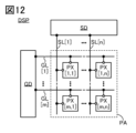
- FIG. 12 is a block diagram showing an example of a display device.
- 13A and 13B are block diagrams showing an example of a drive circuit.
- FIG. 14 is a circuit diagram showing an example of a circuit included in the drive circuit.
- FIG. 15 is a timing chart showing an example of the operation of circuits included in the drive circuit.
- FIG. 16 is a circuit diagram showing an example of a circuit included in the drive circuit.
- FIG. 17 is a circuit diagram showing an example of a circuit included in the drive circuit.
- FIG. 18 is a circuit diagram showing an example of a circuit included in the drive circuit.
- FIG. 19 is a circuit diagram showing an example of a circuit included in the drive circuit.
- FIG. 20 is a block diagram showing an example of a drive circuit.
- FIG. 20 is a block diagram showing an example of a drive circuit.
- FIG. 21 is a timing chart showing an example of the operation of the drive circuit.
- FIG. 22 is a circuit diagram showing an example of a circuit included in the drive circuit.
- FIG. 23 is a circuit diagram showing an example of a circuit included in the drive circuit.
- FIG. 24 is a circuit diagram showing an example of a circuit included in the drive circuit.
- FIG. 25A and FIG. 25B are perspective schematic diagrams showing a configuration example of a display device.
- FIG. 26 is a block diagram showing an example of the configuration of a display device.
- FIG. 27 is a schematic cross-sectional view showing a configuration example of a display device.
- 28A to 28C are schematic cross-sectional views showing configuration examples of a display device.
- FIG. 29 is a schematic cross-sectional view showing a configuration example of a display device.
- FIGS. 30A and 30B are schematic cross-sectional views illustrating a configuration example of a transistor included in a semiconductor device.
- FIG. 31 is a schematic cross-sectional view showing a configuration example of a transistor included in a semiconductor device.
- FIG. 32 is a schematic cross-sectional view showing a configuration example of a display device.
- 33A to 33C are schematic plan views showing examples of the structure of transistors included in a semiconductor device, and
- FIG. 33D is a schematic cross-sectional view showing an example of the structure of transistors included in the semiconductor device.
- FIG. 34A is a schematic plan view showing an example of the structure of a transistor included in a semiconductor device, and FIG.
- FIG. 34B is a schematic cross-sectional view showing an example of the structure of a transistor included in the semiconductor device.
- FIG. 35 is a schematic cross-sectional view showing a configuration example of a display device.
- FIG. 36 is a schematic cross-sectional view showing a configuration example of a display device.
- FIG. 37 is a schematic cross-sectional view showing a configuration example of a display device.
- FIG. 38 is a schematic cross-sectional view showing a configuration example of a display device.
- FIG. 39 is a schematic cross-sectional view showing a configuration example of a display device.
- FIG. 40 is a schematic cross-sectional view showing a configuration example of a display device.
- FIG. 41 is a schematic cross-sectional view showing a configuration example of a display device.
- FIG. 42 is a schematic cross-sectional view showing a configuration example of a display device.
- FIG. 43 is a schematic cross-sectional view showing a configuration example of a display device.
- 44A to 44D are schematic cross-sectional views showing configuration examples of an LED package.
- 45A and 45B are schematic plan views showing a configuration example of an LED package.
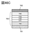
- 46A to 46F are diagrams illustrating configuration examples of light emitting devices.
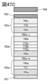
- 47A to 47C are diagrams illustrating configuration examples of light emitting devices.
- FIG. 48A is a circuit diagram showing an example of the configuration of a pixel circuit included in the display device
- FIG. 48B is a schematic perspective view showing an example of the configuration of the pixel circuit included in the display device.
- 49A to 49G are schematic plan views showing examples of pixels.
- 50A to 50F are schematic plan views showing examples of pixels.
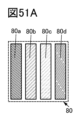
- 51A to 51H are schematic plan views showing examples of pixels.
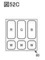
- 52A to 52D are schematic plan views showing examples of pixels.
- 53A to 53G are schematic plan views showing examples of pixels.
- 54A to 54I are perspective views showing an example of an electronic device.
- a semiconductor device is a device that utilizes semiconductor characteristics, and refers to a circuit that includes a semiconductor element (for example, a transistor, a diode, and a photodiode), and a device that has the same circuit.
- semiconductor device refers to any device that can function by utilizing semiconductor characteristics.
- An example of a semiconductor device is an integrated circuit.
- an example of a semiconductor device is a chip including an integrated circuit.
- Another example of a semiconductor device is an electronic component in which a chip is housed in a package.
- a storage device, a display device, a light emitting device, a lighting device, and an electronic device may themselves be a semiconductor device or include a semiconductor device.
- X and Y are electrically connected is an element that enables electrical connection between X and Y (for example, a switch, a transistor, a capacitive element, an inductor, a resistive element, a diode, a display device, light emitting device, and load) can be connected between X and Y.
- the switch has a function of controlling on/off. In other words, the switch is in a conductive state (on state) or in a non-conductive state (off state), and has the function of controlling whether or not current flows.
- both an element and a power supply line are arranged between X and Y.
- a power supply line for example, VDD (high power supply potential), VSS (low power supply potential), GND (ground potential), or a wiring that provides a desired potential
- VDD high power supply potential
- VSS low power supply potential
- GND ground potential
- a wiring that provides a desired potential are arranged between X and Y.
- a transistor if the drain and source of the transistor are interposed between X and Y, it is defined that X and Y are electrically connected.
- a capacitive element when a capacitive element is placed between X and Y, it may or may not be specified that X and Y are electrically connected.
- a capacitive element in the configuration of a digital circuit or logic circuit, if a capacitive element is placed between X and Y, it may not be specified that X and Y are electrically connected.
- a capacitive element is disposed between X and Y, it may be specified that X and Y are electrically connected.
- An example of a case where X and Y are functionally connected is a circuit that enables functional connection between X and Y (for example, a logic circuit (for example, an inverter, a NAND circuit, and a NOR circuit), a signal Conversion circuits (for example, digital-to-analog conversion circuits, analog-to-digital conversion circuits, and gamma correction circuits), potential level conversion circuits (for example, power supply circuits such as booster circuits or step-down circuits, and level shifter circuits that change the potential level of signals), voltage sources, Current sources, switching circuits, amplifier circuits (e.g., circuits that can increase signal amplitude or current amount, operational amplifiers, differential amplifier circuits, source follower circuits, and buffer circuits), signal generation circuits, storage circuits, and control circuits) are It is possible for one or more to be connected between and Y. As an example, even if another circuit is sandwiched between X and Y, if a signal output from X is transmitted
- X, Y, the source (sometimes translated as one of the first terminal and the second terminal) and the drain (sometimes translated as the other of the first terminal and the second terminal) of the transistor are mutually They are electrically connected in the order of X, the source of the transistor, the drain of the transistor, and Y.” or "The source of the transistor is electrically connected to X, the drain of the transistor is electrically connected to Y, and X, the source of the transistor, the drain of the transistor, and Y are electrically connected in this order.” It can be expressed as "there is”.
- X is electrically connected to Y via the source and drain of the transistor, and X, the source of the transistor, the drain of the transistor, and Y are provided in this connection order.” Can be done.
- X and Y are assumed to be objects (for example, devices, elements, circuits, wiring, electrodes, terminals, conductive films or layers).
- a “resistance element” can be, for example, a circuit element having a resistance value higher than 0 ⁇ or a wiring having a resistance value higher than 0 ⁇ . Therefore, in this specification and the like, a “resistance element” includes a wiring having a resistance value, a transistor through which a current flows between a source and a drain, a diode, or a coil. Therefore, the term “resistance element” may be translated into the terms “resistance", “load”, or "region having a resistance value”.
- the resistance value may be, for example, preferably 1 m ⁇ or more and 10 ⁇ or less, more preferably 5 m ⁇ or more and 5 ⁇ or less, and still more preferably 10 m ⁇ or more and 1 ⁇ or less. Further, for example, the resistance may be greater than or equal to 1 ⁇ and less than or equal to 1 ⁇ 10 9 ⁇ .
- a “capacitive element” refers to, for example, a circuit element having a capacitance value higher than 0F, a wiring region having a capacitance value higher than 0F, a parasitic capacitance, or a transistor.
- the gate capacitance can be Further, the term “capacitive element,” “parasitic capacitance,” or “gate capacitance” can sometimes be replaced with the term “capacitance.” Conversely, the term “capacitance” may be translated into the terms “capacitive element,” “parasitic capacitance,” or “gate capacitance.” Further, a “capacitive element” (including a “capacitive element” having three or more terminals) has a configuration including an insulator and a pair of conductors sandwiching the insulator.
- a pair of conductors in a “capacitive element” can be translated into a “pair of electrodes," a “pair of conductive regions,” a “pair of regions,” or a “pair of terminals.” Further, the terms “one of a pair of terminals” and “the other of a pair of terminals” may be referred to as a first terminal and a second terminal, respectively.
- the value of the capacitance can be, for example, 0.05 fF or more and 10 pF or less. Further, for example, it may be set to 1 pF or more and 10 ⁇ F or less.
- a transistor has three terminals called a gate, a source, and a drain.
- the gate is a control terminal that controls the conduction state of the transistor.
- the two terminals that function as sources or drains are input/output terminals of the transistor.
- One of the two input/output terminals becomes a source and the other becomes a drain depending on the conductivity type of the transistor (n-channel type, p-channel type) and the level of potential applied to the three terminals of the transistor. Therefore, in this specification and the like, the terms source and drain may be used interchangeably.
- a multi-gate structure transistor having two or more gate electrodes can be used as an example of a transistor.
- a multi-gate structure channel formation regions are connected in series, resulting in a structure in which a plurality of transistors are connected in series. Therefore, the multi-gate structure can reduce off-state current and improve the breakdown voltage (improve reliability) of the transistor.
- the multi-gate structure when operating in the saturation region, even if the voltage between the drain and source changes, the current between the drain and source does not change much, and the slope is flat. characteristics can be obtained. By utilizing voltage/current characteristics with a flat slope, it is possible to realize an ideal current source circuit or an active load with a very high resistance value. As a result, a differential circuit or a current mirror circuit with good characteristics can be realized.
- the circuit element may include multiple circuit elements.
- this also includes the case where two or more resistors are electrically connected in series.
- this also includes a case where two or more capacitive elements are electrically connected in parallel.
- one transistor is shown on the circuit diagram, two or more transistors are electrically connected in series, and the gates of each transistor are electrically connected to each other. shall be included.
- the switch has two or more transistors, and the two or more transistors are electrically connected in series or parallel. , including the case where the gates of the respective transistors are electrically connected to each other.
- a node can be translated as a terminal, wiring, electrode, conductive layer, conductor, or impurity region depending on the circuit configuration and device structure. Furthermore, terminals, wiring, etc. can be referred to as nodes.
- Voltage refers to a potential difference from a reference potential.
- the reference potential is a ground potential (earth potential)
- “voltage” can be translated into “potential.” Note that the ground potential does not necessarily mean 0V.
- potential is relative, and as the reference potential changes, the potential applied to wiring, the potential applied to circuits, etc., the potential output from circuits, etc. also change.
- the terms “high-level potential” and “low-level potential” do not mean specific potentials.
- the respective high-level potentials provided by both wires do not have to be equal to each other.
- the low-level potentials provided by both wires do not have to be equal to each other.
- current refers to the phenomenon of charge movement (electrical conduction), and for example, the statement that "electrical conduction of a positively charged body is occurring” is replaced by “in the opposite direction, electrical conduction of a negatively charged body is occurring.” In other words, “electrical conduction is occurring.” Therefore, in this specification and the like, “current” refers to a charge movement phenomenon (electrical conduction) accompanying the movement of carriers, unless otherwise specified. Examples of carriers here include electrons, holes, anions, cations, and complex ions, and carriers differ depending on the system in which current flows (eg, semiconductor, metal, electrolyte, and in vacuum). Furthermore, the "direction of current” in wiring, etc.
- ordinal numbers such as “first,” “second,” and “third” are added to avoid confusion between constituent elements. Therefore, the number of components is not limited. Further, the order of the constituent elements is not limited. For example, a component referred to as “first” in one embodiment of this specification etc. may be a component referred to as “second” in another embodiment or in the claims. It's also possible. Furthermore, for example, a component referred to as “first” in one of the embodiments of this specification etc. may be omitted in other embodiments or claims.
- the terms “above” and “below” do not limit the positional relationship of the components to be directly above or below, and in direct contact with each other.
- electrode B does not need to be formed directly on insulating layer A, and there is no need to form another structure between insulating layer A and electrode B. Do not exclude things that contain elements.
- electrode B does not need to be formed on insulating layer A in direct contact with insulating layer A and electrode B. Do not exclude items that include other components between them.
- electrode B below the insulating layer A it is not necessary that the electrode B is formed under the insulating layer A in direct contact with the insulating layer A and the electrode B. Do not exclude items that include other components between them.
- words such as “row” and “column” may be used to describe components arranged in a matrix and their positional relationships. Further, the positional relationship between the components changes as appropriate depending on the direction in which each component is depicted. Therefore, the terms are not limited to those explained in the specification, etc., and can be appropriately rephrased depending on the situation. For example, the expression “row direction” may be translated into “column direction” by rotating the orientation of the drawing by 90 degrees.
- the words “film” and “layer” can be interchanged depending on the situation.
- the term “conductive layer” may be changed to the term “conductive film.”
- the term “insulating film” may be changed to the term “insulating layer.”
- the words “film” and “layer” may be omitted and replaced with other terms.
- the term “conductive layer” or “conductive film” may be changed to the term “conductor.”
- the term “insulating layer” or “insulating film” may be changed to the term "insulator.”
- the terms “electrode,” “wiring,” and “terminal” do not functionally limit these components.
- an “electrode” may be used as part of a “wiring” and vice versa.
- the terms “electrode” or “wiring” include cases where a plurality of “electrodes” or “wirings” are formed integrally.
- a “terminal” may be used as part of a “wiring” or “electrode,” and vice versa.
- the term “terminal” also includes cases in which one or more selected from “electrode,” “wiring,” and “terminal” are integrally formed.
- an “electrode” can be a part of a “wiring” or a “terminal,” and, for example, a “terminal” can be a part of a “wiring” or a “electrode.”
- the term “electrode,” “wiring,” or “terminal” may be replaced with the term “region” depending on the case.
- terms such as “wiring,” “signal line,” and “power line” can be interchanged depending on the case or the situation.
- the term “signal line” or “power line” may be changed to the term “wiring” in some cases.
- the term “power line” may be changed to the term "signal line”.
- the term “signal line” may be changed to the term "power line”.
- the term “potential” applied to the wiring may be changed to the term “signal”.
- the term “signal” may be changed to the term “potential”.
- timing charts may be used to explain the operating method of a semiconductor device.
- the timing charts used in this specification etc. show ideal operation examples, and the periods, magnitudes of signals (for example, potential or current), and timings described in the timing charts are , unless otherwise specified.
- the timing charts described in this specification etc. may change the magnitude and timing of a signal (e.g., potential or current) input to each wiring (including a node) in the timing chart depending on the situation. It can be performed. For example, even if two periods are written at equal intervals in the timing chart, the lengths of the two periods may be different from each other. Also, for example, even if one period is long and the other short, the lengths of both periods may be equal, or one period may be short. In some cases, the other period may be made longer.
- metal oxide refers to a metal oxide in a broad sense.
- Metal oxides are classified into oxide insulators, oxide conductors (including transparent oxide conductors), oxide semiconductors (also referred to as oxide semiconductors or simply OS), and the like.
- oxide semiconductors also referred to as oxide semiconductors or simply OS
- the metal oxide is sometimes referred to as an oxide semiconductor.
- a metal oxide can constitute a channel forming region of a transistor having at least one of an amplification effect, a rectification effect, and a switching effect
- the metal oxide is called a metal oxide semiconductor. be able to.
- OS transistor it can be referred to as a transistor including a metal oxide or an oxide semiconductor.
- metal oxides containing nitrogen may also be collectively referred to as metal oxides.
- a metal oxide containing nitrogen may be referred to as a metal oxynitride.
- semiconductor impurities refer to, for example, substances other than the main components that constitute the semiconductor layer.
- an element having a concentration of less than 0.1 atomic % is an impurity.
- impurities include, for example, an increase in the defect level density of the semiconductor, a decrease in carrier mobility, and a decrease in crystallinity.
- impurities that change the characteristics of the semiconductor include, for example, group 1 elements, group 2 elements, group 13 elements, group 14 elements, and group 15 elements.
- transition metals other than the main components in particular, for example, hydrogen (also present in water), lithium, sodium, silicon, boron, phosphorus, carbon and nitrogen.
- a switch refers to a switch that is in a conductive state (on state) or a non-conductive state (off state) and has the function of controlling whether or not current flows.
- a switch refers to a device that has the function of selecting and switching a path through which current flows. Therefore, a switch may have two or more terminals through which current flows, in addition to the control terminal.
- an electrical switch, a mechanical switch, etc. can be used. In other words, the switch is not limited to a specific type as long as it can control the current.
- Examples of electrical switches include transistors (e.g., bipolar transistors, MOS transistors, etc.), diodes (e.g., PN diodes, PIN diodes, Schottky diodes, MIM (Metal Insulator Metal) diodes, and MIS (Metal Insulator Semiconductor) diodes. de , diode-connected transistors, etc.), or logic circuits that combine these.
- transistors e.g., bipolar transistors, MOS transistors, etc.
- diodes e.g., PN diodes, PIN diodes, Schottky diodes, MIM (Metal Insulator Metal) diodes, and MIS (Metal Insulator Semiconductor) diodes. de , diode-connected transistors, etc.
- the "conducting state" of the transistor means, for example, a state in which the source and drain electrodes of the transistor can be considered to be electrically short-circuited, or a state in which there
- non-conducting state of a transistor refers to a state in which the source electrode and drain electrode of the transistor can be considered to be electrically disconnected. Note that when the transistor is operated as a simple switch, the polarity (conductivity type) of the transistor is not particularly limited.
- a mechanical switch is a switch using MEMS (micro electro mechanical systems) technology.
- the switch has an electrode that can be moved mechanically, and operates by controlling conduction and non-conduction by moving the electrode.
- a device manufactured using a metal mask or FMM may be referred to as a device with a MM (metal mask) structure.
- a device manufactured without using a metal mask or FMM may be referred to as a device with an MML (metal maskless) structure.
- a structure in which a light-emitting layer is made separately or a structure in which the light-emitting layer is painted separately for each color light-emitting device is referred to as SBS (Side By).
- SBS Side By
- a light emitting device that can emit white light may be referred to as a white light emitting device.
- a white light-emitting device can be combined with a colored layer (for example, a color filter) to form a full-color display device.
- light emitting devices can be broadly classified into single structures and tandem structures. It is preferable that a device with a single structure has one light-emitting unit between a pair of electrodes, and that the light-emitting unit includes one or more light-emitting layers.
- the light-emitting layers may be selected such that the colors of each of the two light-emitting layers are complementary colors. For example, by making the light emitting color of the first light emitting layer and the light emitting color of the second light emitting layer complementary, it is possible to obtain a configuration in which the light emitting device as a whole emits white light.
- the structure when obtaining white light emission using three or more light emitting layers, the structure may be such that the light emitting device as a whole can emit white light by combining the respective emitted light colors of the three or more light emitting layers.
- the tandem structure device has two or more light emitting units between a pair of electrodes, and each light emitting unit includes one or more light emitting layers.
- a configuration may be adopted in which white light emission can be obtained by combining light from the light emitting layers of a plurality of light emitting units.
- the configuration for obtaining white light emission is the same as the configuration of the single structure.
- the SBS structure light emitting device can have lower power consumption than the white light emitting device. If it is desired to keep power consumption low, it is preferable to use a light emitting device with an SBS structure.
- a white light-emitting device is preferable because the manufacturing process is simpler than that of a light-emitting device with an SBS structure, and thus the manufacturing cost can be lowered or the manufacturing yield can be increased.
- parallel refers to a state in which two straight lines are arranged at an angle of -10° or more and 10° or less. Therefore, the case where the angle is greater than or equal to -5° and less than or equal to 5° is also included.
- substantially parallel or “substantially parallel” refers to a state in which two straight lines are arranged at an angle of -30° or more and 30° or less.
- perpendicular refers to a state in which two straight lines are arranged at an angle of 80° or more and 100° or less. Therefore, the case where the angle is 85° or more and 95° or less is also included.
- substantially perpendicular or “approximately perpendicular” refers to a state in which two straight lines are arranged at an angle of 60° or more and 120° or less.
- each embodiment can be appropriately combined with the structure shown in other embodiments to form one embodiment of the present invention. Further, when a plurality of configuration examples are shown in one embodiment, it is possible to combine the configuration examples with each other as appropriate.
- content (or even part of the content) described in one embodiment may be different from other content (or even part of the content) described in that embodiment and one or more other implementations. It is possible to apply, combine, or replace at least one content with the content described in the form (or even a part of the content).
- a diagram (which may be a part) described in one embodiment may be a different part of that diagram, another diagram (which may be a part) described in that embodiment, and one or more other parts. More figures can be configured by combining at least one figure (or even a part) described in the embodiment.
- the code when the same code is used for multiple elements, especially when it is necessary to distinguish between them, the code includes an identifying symbol such as "_1", “[n]”, “[m,n]”, etc. In some cases, the symbol may be added to the description. In addition, in the drawings, etc., when a code for identification such as “_1”, “[n]”, “[m,n]”, etc. is added to the code, when there is no need to distinguish it in this specification etc. In some cases, no identification code is written.
- the circuit BSPR shown in FIG. 2A is an example of an amplifier circuit, and includes a circuit BB, a transistor MNb, and a capacitive element Ca. Further, the circuit BSPR includes, for example, a terminal Ti that functions as an input terminal and a terminal To that functions as an output terminal. Further, the circuit BB has, for example, a terminal Bi that functions as an input terminal and a terminal Bo that functions as an output terminal.
- an OS transistor as the transistor MNb.
- metal oxides included in the channel forming region of the OS transistor include In-M-Zn oxide containing indium, element M, and zinc (element M is aluminum, gallium, yttrium, tin, copper, vanadium). , beryllium, boron, titanium, iron, nickel, germanium, zirconium, molybdenum, lanthanum, cerium, neodymium, hafnium, tantalum, tungsten, cobalt, magnesium, or antimony).
- a transistor having silicon in a channel formation region hereinafter referred to as a Si transistor may be applied.
- Transistors other than OS transistors and Si transistors include, for example, transistors whose channel formation region contains germanium (Ge), zinc selenide (ZnSe), cadmium sulfide (CdS), gallium arsenide (GaAs), etc. , a transistor whose channel formation region contains a compound semiconductor such as indium phosphide (InP), gallium nitride (GaN), or silicon germanium (SiGe), a transistor whose channel formation region contains carbon nanotubes, or a transistor whose channel formation region contains an organic semiconductor.
- a transistor included in the region can be used.
- the transistor MNb illustrated in FIG. 2A is, for example, an n-channel transistor with a multi-gate structure having gates above and below the channel, and the transistor MNb has a first gate and a second gate.
- the first gate is sometimes described as a gate (sometimes referred to as a front gate)
- the second gate is sometimes described as a back gate.
- the first gate and the second gate can be interchanged with each other, and therefore the word “gate” can be written interchangeably with the word “back gate.”
- the phrase “back gate” can be written interchangeably with the phrase “gate.”
- a connection configuration such as “the gate is electrically connected to the first wiring, and the back gate is electrically connected to the second wiring” is equivalent to "the back gate is electrically connected to the first wiring”. and the gate is electrically connected to the second wiring.
- the connection configuration of the back gate is not illustrated.
- the electrical connection destination of the back gate can be determined at the design stage.
- the gate and the back gate may be electrically connected in order to increase the on-state current of the transistor. That is, for example, the gate and back gate of transistor MNb may be electrically connected.
- the back gate of the transistor in order to vary the threshold voltage of the transistor or to reduce the off-state current of the transistor, the back gate of the transistor may be electrically connected to an external circuit.
- a configuration may also be adopted in which a wiring is provided for this purpose and a potential is applied to the back gate of the transistor by the external circuit.
- the transistor MNb is ideally normally off, and the threshold voltage of the transistor MNb is set to V th_MNb .
- the threshold voltage V th_MNb is a voltage that satisfies V High ⁇ V Low >V th_MNb . Note that V High is a high level potential, and V Low is a low level potential.
- normally-off refers to a state in which no current flows through a transistor when the gate-source voltage is 0V.
- normally-off in an OS transistor means that when the gate-source voltage is 0V, the current flowing through the transistor per 1 ⁇ m of channel width is 1 ⁇ 10 ⁇ 20 A or less at room temperature and 1 ⁇ 10 ⁇ 20 A at 85°C . 18 A or less, or 1 ⁇ 10 ⁇ 16 A or less at 125°C.
- normally-on refers to a state in which a channel exists even when the gate-source voltage is 0V, and current flows through the transistor.
- the semiconductor device of one embodiment of the present invention does not depend on the structure of a transistor included in the semiconductor device.
- the transistor MNb illustrated in FIG. 2A may have a configuration without a back gate, that is, a transistor with a single gate structure (see FIG. 2B). Further, some transistors may have a back gate, and some other transistors may have a back gate.
- the transistor MNb is an n-channel transistor, but depending on the situation, the transistor MNb may be a p-channel transistor.
- the terminal Bi of the circuit BB is electrically connected to the terminal Ti, and the terminal Bo of the circuit BB is electrically connected to the gate of the transistor MNb and the first terminal of the capacitive element Ca. Further, the first terminal of the transistor MNb is electrically connected to the wiring VAL1, and the second terminal of the transistor MNb is electrically connected to the second terminal of the capacitive element Ca and the terminal To.
- the electrical connection portion between the terminal Bo of the circuit BB, the gate of the transistor MNb, and the first terminal of the capacitive element Ca is referred to as a node N.
- the circuit BB has, for example, a function of setting the node N in a floating state. Therefore, the circuit BB can be configured to include a switching element, for example. Further, the circuit BB has a function of outputting a potential corresponding to the potential input to the terminal Bi to the terminal Bo. For example, the circuit BB may be configured to output the potential V Mid to the terminal Bo when the high level potential V High is applied to the terminal Bi. Note that V Mid is a potential lower than the high level potential V High and higher than the low level potential V Low . Further, V Mid is a voltage that satisfies V Mid ⁇ V Low > V th_MNb .
- the wiring VAL1 in FIG. 2A functions as a wiring that provides a fixed potential or a variable potential, for example.
- the fixed potential include a high level potential, a low level potential, a ground potential, and a negative potential.
- a pulse signal (sometimes referred to as a pulse voltage) can be mentioned.
- a clock signal can be cited as an example of a pulse signal.
- the potential of the terminal Ti is indicated as V in
- the potential of the terminal To is indicated as V out .
- the potential of the node N of the circuit BSPR in FIG. 2A is a potential V Mid lower than the high level potential V High . Further, at this time, it is assumed that the node N is not in a floating state. Further, it is assumed that a low level potential V Low is applied from the wiring VAL1 to the first terminal of the transistor MNb.
- the potential of the node N is in a floating state, due to the capacitive coupling of the capacitive element Ca, as the potential of the terminal To increases, the potential of the node N also increases from V Mid . As a result, the gate-source voltage of the transistor MNb is held by the capacitive element Ca, so that the potential of the terminal To increases to V High . Further, ideally, the potential of the node N is V Mid +V High - V Low .
- the circuit BSPR is as shown in FIG. 2C. , it is possible to have a configuration in which the capacitive element Ca is not provided. In this case, the circuit area of the circuit BSPR can be reduced.
- the potential of the terminal Ti of the circuit BSPR when the potential of the terminal Ti of the circuit BSPR is V High and the terminal Ti is in a floating state (not electrically connected to the wiring that provides the potential), the potential of the terminal Ti may change due to various factors. There is. For example, in a transistor for holding the potential of terminal Ti, if the off-state current flowing between the source and drain or the leakage current flowing between the gate and source or between the gate and drain increases, the potential of the terminal Ti will fluctuate. . Furthermore, when a noise signal is input to the terminal Ti, the potential of the terminal Ti also fluctuates. That is, since the potential applied to the terminal Bi of the circuit BB fluctuates, it also affects the potential of the node N, and as a result, the potential output from the terminal To of the circuit BSPR may become unstable.
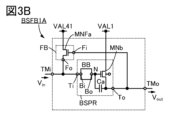
- FIG. 1A shows an amplifier circuit that is a semiconductor device of one embodiment of the present invention that solves the above problems.
- the circuit BSFB shown in FIG. 1A is a circuit including the circuit BSPR of FIG. 2A and the circuit FB.
- the circuit FB has a terminal Fi and a terminal Fo.
- the terminal Ti of the circuit BSPR and the terminal Fo of the circuit FB are electrically connected to each other. Further, the terminal To of the circuit BSPR and the terminal Fi of the circuit FB are electrically connected to each other. Note that in FIG. 1A, the terminal Ti of the circuit BSPR and the terminal Fo of the circuit FB are collectively shown as one terminal TMi, and the terminal To of the circuit BSPR and the terminal Fi of the circuit FB are collectively shown as one terminal TMi. It is illustrated as a terminal TMo.
- the circuit FB has a function of acquiring the potential output from the terminal To of the circuit BSPR and applying a fixed potential to the terminal Ti of the circuit BSPR.
- the circuit FB can be said to be a circuit that provides feedback to the circuit BSPR based on the potential output from the terminal To of the circuit BSPR.
- the circuit FB may be configured to output a fixed potential (for example, high-level potential V High ) to the terminal Fo when the high-level potential V High is input to the terminal Fi.
- the circuit FB By configuring the circuit FB as described above, for example, when the high level potential V High is being output from the terminal To of the circuit BSPR, the fixed potential output from the terminal Fo of the circuit FB is applied to the terminal Ti of the circuit BSPR. is given. For this reason, for example, in a transistor for holding the potential of terminal Ti (terminal TMi), even if the off-state current flowing between the source and drain or the leakage current flowing between the gate and source or between the gate and drain becomes large, , the potential of the terminal Ti (terminal TMi) remains at the fixed potential given by the circuit FB.
- the potential of the terminal Ti (terminal TMi) remains at the fixed potential provided by the circuit FB. Therefore, since the potential at the terminal To of the circuit BSPR does not change due to the above-mentioned factors, the potential at the node N is also unlikely to be affected. Therefore, the potential output from the terminal To of the circuit BSPR becomes stable.
- the semiconductor device of one embodiment of the present invention is not limited to the circuit BSFB shown in FIG. 1A.
- the semiconductor device of one embodiment of the present invention may have a structure in which a transistor MNg is provided in the circuit BSFB in FIG. 1A, for example, as in the circuit BSFBA shown in FIG. 1B.
- a transistor applicable to the transistor MNb can be used as the transistor MNg.
- the circuit BSFBA in FIG. 1B includes a terminal TMi1 and a terminal TMi2 that function as input terminals, and a terminal TMo that functions as an output terminal.
- the terminal TMi1 corresponds to the terminal TMi shown in FIG. 1A.
- the potential of the terminal TMi1 is indicated as V in1
- the potential of the terminal TMi2 is indicated as V in2 .
- the first terminal of the transistor MNg is electrically connected to the second terminal of the transistor MNb, the second terminal of the capacitive element Ca, and the terminal TMo. Further, the second terminal of the transistor MNg is electrically connected to the wiring VAL4. Further, the gate of the transistor MNg is electrically connected to the terminal TMi2.
- the wiring VAL4 functions as a wiring that provides a fixed potential, for example.
- the fixed potential include a low level potential.
- other fixed potentials include a ground potential or a negative potential.
- the wiring VAL4 may function as a wiring that provides a variable potential.
- the circuit BSFBA can output the low level potential V Low from the terminal TMo when the wiring VAL4 is a wiring that outputs the low level potential V Low .
- the low level potential V Low is input to the terminal TMi2 to turn off the transistor MNg. Thereafter, by inputting the high level potential V High to the terminal TMi1, the high level potential V High is output from the terminal TMo.
- the operation example of the circuit BSFB in FIG. 1A can be referred to for the operation in which the high-level potential V High is output from the terminal TMo.
- the transistor MNg when outputting the low level potential V Low from the terminal TMo of the circuit BSFBA, the transistor MNg may be turned on by inputting the high level potential V High to the terminal TMi2. As a result, conduction is established between the terminal TMo and the wiring VAL4, so that the charge accumulated in the terminal TMo flows to the wiring VAL4, and as a result, the potential of the terminal TMo becomes the low level potential V Low .
- the transistor MNb is turned off, and the connection between the wiring VAL1 and the terminal TMo is Since the terminal TMo is in a non-conducting state, the potential at the terminal TMo can quickly fall to the low level potential V Low .
- the semiconductor device of one embodiment of the present invention may have a structure in which the capacitive element Ca is not provided in the circuit BSPR, for example, as in the circuit BSFBB illustrated in FIG. 1C.
- the circuit BSFBB in FIG. 1C has a configuration in which the circuit BSPR in FIG. 1A is replaced with the circuit BSPR in FIG. 2C.
- FIG. 2C when the gate capacitance of the transistor MNb is large, it is not necessary to provide the capacitive element Ca in the circuit BSPR in FIG. 1A, and this reduces the circuit area of the circuit BSFB in FIG. 1A. be able to.
- the circuit BSFB1 shown in FIG. 3A has a configuration in which the circuit FB includes a transistor MNFa.
- a transistor applicable to the transistor MNb can be used as the transistor MNFa.
- the transistor MNFa is illustrated as an n-channel transistor with a multi-gate structure having gates above and below the channel.
- the first terminal of the transistor MNFa is electrically connected to the terminal Fo, and the second terminal of the transistor MNFa is electrically connected to the wiring VAL41. Further, the gate of the transistor MNFa is electrically connected to the terminal Fi.
- the wiring VAL41 functions as a wiring that provides a fixed potential or a variable potential, similar to the wiring VAL1.
- the fixed potential include a high level potential, a low level potential, a ground potential, and a negative potential.
- a pulse signal (sometimes referred to as a pulse voltage) can be mentioned.
- the wiring VAL41 may be electrically connected to the wiring VAL1.
- the wiring VAL41 may be the same wiring as the wiring VAL1.
- the example of the operation of the circuit BSPR in FIG. 2A can be referred to.
- V Mid is applied to the gate of transistor MNb (first terminal of capacitive element Ca).
- a low level potential V Low is applied from the wiring VAL1 to the first terminal of the transistor MNb.
- a high level potential V High is applied from the wiring VAL41 to the second terminal of the transistor MNFa.
- V Low which is the same as the potential of the terminal To, is input to the terminal Fi of the circuit FB.
- a low level potential V Low is applied to the gate of the transistor MNFa.
- the transistor MNFa is normally off, and the threshold voltage of the transistor MNFa is set to V th_MNFa . Further, the threshold voltage V th_MNFa is a voltage that satisfies V High ⁇ V Low >V th_MNFa .
- the transistor MNFa Since the voltage between the gate and the source of the transistor MNFa (here, the voltage between the gate and the first terminal) satisfies V Low - V High ⁇ V th_MNFa , the transistor MNFa is turned off.
- the potential of the node N is in a floating state, due to the capacitive coupling of the capacitive element Ca, as the potential of the terminal To increases, the potential of the node N also increases from V Mid . As a result, the gate-source voltage of the transistor MNb is held by the capacitive element Ca, so that the potential of the terminal To increases to V High . Further, ideally, the potential of the node N is V Mid +V High - V Low .
- V High which is the same potential as the terminal To, is input to the terminal Fi of the circuit FB.
- V High is applied to the gate of the transistor MNFa.
- the potential of the terminal Ti (the first terminal of the transistor MNFa) of the circuit BSPR decreases from the high level potential V High , and the voltage between the gate and the first terminal of the transistor MNFa becomes higher than the threshold voltage.
- the transistor MNFa is turned on.
- charges from the wiring VAL41 are accumulated in the terminal Ti of the circuit BSPR, and the potential of the terminal Ti of the circuit BSPR increases.
- the transistor MNFa is turned off when the gate-source voltage of the transistor MNFa reaches V th_MNFa , so the potential of the terminal Ti (the first terminal of the transistor MNFa) of the circuit BSPR at this time is V High ⁇ V th_MNFa .
- the circuit FB1 when the high-level potential V High is output from the terminal TMo, and when the potential of the terminal Ti of the circuit BSPR falls, the circuit FB increases the potential V High -V th_MNFa with respect to the terminal Ti. can be given. As a result, the potential of the terminal Ti is maintained at approximately V High -V th_MNFa , so the potential output from the terminal To of the circuit BSPR becomes stable.
- the semiconductor device of one embodiment of the present invention is not limited to the circuit BSFB1 shown in FIG. 3A.
- the semiconductor device of one embodiment of the present invention may have a structure in which the transistor MNFa has a single-gate structure, for example, as in the circuit BSFB1A illustrated in FIG. 3B.
- the transistor MNFa may be a transistor without a back gate.
- the semiconductor device of one embodiment of the present invention may have a structure in which a transistor MNg is provided in the circuit BSFB1 in FIG. 3A, for example, as in the circuit BSFB1B illustrated in FIG. 3C.
- the circuit BSFB1B in FIG. 3C has a configuration in which the circuit FB shown in FIG. 3A is applied to the circuit FB in the circuit BSFBA in FIG. 1B.
- the circuit BSFB1B like the circuit BSFBA of FIG. 1B, is an amplifier circuit that can output a high level potential V High or a low level potential V Low from the terminal TMo.
- the circuit BSFB2 shown in FIG. 4A is a modification of the circuit BSFB1 in FIG. 3A, and differs from the circuit BSFB1 in that the back gate of the transistor MNFa is electrically connected to the gate of the transistor MNFa.
- the on-state current of the transistor can be increased. That is, by electrically connecting the gate and back gate of the transistor MNFa of the circuit BSFB2, it is possible to increase the on-current that flows when the transistor MNFa is in the on state. Thereby, the speed at which the potential of the terminal TMi changes to the fixed potential (for example, V High ⁇ V th_MNFa ) output from the terminal Fo of the circuit FB can be increased.
- circuit BSFB3 shown in FIG. 4B is a modification of the circuit BSFB1 in FIG. 3A, and differs from the circuit BSFB1 in that the back gate of the transistor MNFa is electrically connected to the wiring VAL51.
- the wiring VAL51 functions as a wiring that provides a fixed potential, similar to the wiring VAL4.
- examples of the fixed potential include a low level potential.
- other fixed potentials include a ground potential or a negative potential.
- the wiring VAL51 may function as a wiring that provides a variable potential.
- the threshold voltage of the transistor MNFa increases. Thereby, the transistor MNFa can be normally turned off, so that the off-state current flowing between the source and drain of the transistor MNFa can be reduced.
- circuit BSFB4 shown in FIG. 4C is a modification of the circuit BSFB1 in FIG. 3A, in that the back gate of the transistor MNFa is electrically connected to the terminal TMi, the terminal Fo, and the terminal Ti. This circuit is different from circuit BSFB1.
- the low level potential V Low When the low level potential V Low is input to the terminal TMi of the transistor MNFa in the circuit BSFB4, the low level potential V Low is input to the back gate of the transistor MNFa, so that the threshold voltage of the transistor MNFa increases. Further, at this time, when the low level potential V Low is output from the terminal TMo, the low level potential V Low is input to the gate of the transistor MNFa, so the transistor MNFa is turned off, and the transistor MNFa at this time The amount of off-state current flowing between the source and drain of the transistor can be reduced.
- the transistor MNFa in the circuit BSFB4 when the high level potential V High is input to the terminal TMi, the high level potential V High is input to the back gate of the transistor MNFa, so the threshold voltage of the transistor MNFa is low. Become. Furthermore, at this time, when the high level potential V High is output to the terminal TMo due to the operation of the circuit BSPR, the transistor MNFa is turned on because the high level potential V High is input to the gate of the transistor MNFa. . At this time, the amount of on-current flowing between the source and drain of the transistor MNFa increases because the high-level potential V High is input to the back gate of the transistor MNFa. Thereby, the speed at which the potential of the terminal TMi changes to the fixed potential (for example, V High ⁇ V th_MNFa ) output from the terminal Fo of the circuit FB can be increased.
- V High ⁇ V th_MNFa the fixed potential
- circuit BSFB5 shown in FIG. 4D is a modification of the circuit BSFB1 shown in FIG. It is different from That is, the transistor MNFa in the circuit BSFB5 has a diode-connected configuration.
- the potential of the first terminal of the transistor MNFa is V High ⁇ V th_MNFa
- the transistor MNFa is turned on.
- the current output from the terminal To flows to the terminal TMi via the circuit FB and between the source and drain of the transistor MNFa.
- the transistor MNFa is turned off.
- the potential output from the terminal To of the circuit BSPR can be fed back to give a fixed potential to the terminal Ti of the circuit BSPR.
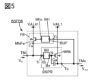
- the circuit BSFB6 shown in FIG. 5 is a modification of the circuit BSFB1 in FIG. 3A, and differs from the circuit BSFB1 in that the circuit FB is provided with a circuit BUF. Further, the terminal Fi of the circuit BSFB6 and the gate of the transistor MNFa are not directly electrically connected to each other, the terminal Fi of the circuit BSFB6 is directly electrically connected to the terminal BFi described later, and the gate of the transistor MNFa is directly electrically connected to the terminal BFi described later. It also differs from the circuit BSFB1 in that it is directly electrically connected to the terminal BFo.
- the circuit BUF has a terminal BFi and a terminal BFo.
- the circuit BUF has a function of amplifying the potential input to the terminal BFi and outputting the amplified potential to the terminal BFo.
- the circuit BUF functions as a buffer circuit.
- circuit BSFB6 by using the circuit BUF as a buffer circuit, for example, even if the potential output from the terminal TMo changes slightly due to a noise signal, etc., a stable fixed potential can be given to the gate of the transistor MNFa. .
- FIG. 6A A configuration example of the circuit BUF of the circuit BSFB6 shown in FIG. 5 is shown in FIG. 6A. Note that, in order to explain the electrical connection configuration, FIG. 6A also shows the circuit BSPR, the terminal TMi, and the terminal TMo.
- the circuit BUF includes a logic circuit INV1 and a logic circuit INV2.
- the input terminal of the logic circuit INV1 is electrically connected to the terminal BFi
- the output terminal of the logic circuit INV1 is electrically connected to the input terminal of the logic circuit INV2
- the output terminal of the logic circuit INV2 is electrically connected to the terminal BFo. connected.
- Each of the logic circuit INV1 and the logic circuit INV2 has a function of generating an inverted signal for a signal input to an input terminal and outputting the inverted signal.
- an inverter circuit can be used as the logic circuit INV1 and the logic circuit INV2.
- other than the inverter circuit for example, a NAND circuit, a NOR circuit, an XOR circuit, or a logic circuit that is a combination of these can be used.
- FIG. 6B shows a configuration example of the logic circuit INV1 and the logic circuit INV2 included in the circuit BUF of the circuit BSFB6A shown in FIG. 6A.
- each of the logic circuit INV1 and the logic circuit INV2 includes a transistor M1, a transistor M2, a transistor M3, and a transistor M4.
- a transistor applicable to the transistor MNb can be used, for example.
- the gate of the transistor M1 and the gate of the transistor M3 are each electrically connected to the input terminal of the logic circuit INV1 (terminal BFi of the circuit BUF). Further, the first terminal of the transistor M1 is electrically connected to the first terminal of the transistor M2 and the gate of the transistor M4. Further, the second terminal of the transistor M1 is electrically connected to the wiring VAL52. Further, the second terminal of the transistor M2 is electrically connected to the gate of the transistor M2 and the wiring VAL42. Further, the first terminal of the transistor M3 is electrically connected to the first terminal of the transistor M4 and the output terminal of the logic circuit INV1. Further, the second terminal of the transistor M3 is electrically connected to the wiring VAL52. Further, the second terminal of the transistor M4 is electrically connected to the wiring VAL42.
- the gate of the transistor M1 and the gate of the transistor M3 are each electrically connected to the input terminal of the logic circuit INV2 (the output terminal of the logic circuit INV1). Further, the first terminal of the transistor M1 is electrically connected to the first terminal of the transistor M2 and the gate of the transistor M4. Further, the second terminal of the transistor M1 is electrically connected to the wiring VAL52. Further, the second terminal of the transistor M2 is electrically connected to the gate of the transistor M2 and the wiring VAL42. Further, the first terminal of the transistor M3 is electrically connected to the first terminal of the transistor M4 and the output terminal of the logic circuit INV2 (terminal BFo of the circuit BUF). Further, the second terminal of the transistor M3 is electrically connected to the wiring VAL52. Further, the second terminal of the transistor M4 is electrically connected to the wiring VAL42.
- the wiring VAL42 functions as a power supply line for applying a high-level potential to each of the logic circuit INV1 and the logic circuit INV2.
- the wiring VAL42 may be a wiring that provides a low-level potential, a ground potential, or a negative potential instead of a high-level potential.
- the wiring VAL42 may be a wiring that provides a variable potential instead of a fixed potential.
- the wiring VAL52 functions as a power supply line for applying a low-level potential to each of the logic circuit INV1 and the logic circuit INV2.
- the wiring VAL52 may be a wiring that provides a high-level potential, a ground potential, or a negative potential instead of a low-level potential.
- the wiring VAL52 may be a wiring that provides a variable potential instead of a fixed potential.
- one wiring VAL42 is electrically connected to the second terminal of the transistor M2 and the second terminal of the transistor M4 included in each of the logic circuit INV1 and the logic circuit INV2. Different wirings may be electrically connected to the second terminal of the transistor M2 and the second terminal of the transistor M4 included in each of the circuit INV1 and the logic circuit INV2.
- one wiring VAL52 is electrically connected to the second terminal of the transistor M1 and the second terminal of the transistor M3 included in each of the logic circuit INV1 and the logic circuit INV2. Different wirings may be electrically connected to the second terminal of the transistor M1 and the second terminal of the transistor M3 included in each of the logic circuit INV1 and the logic circuit INV2.
- FIG. 7A a configuration example of the circuit BUF of the circuit BSFB6 shown in FIG. 5 is shown in FIG. 7A.
- the circuit BSFB6C shown in FIG. 7A is also a modification of the circuit BSFB6B in FIG. 6B, and is different from the circuit BSFB6B in the number of transistors included in the circuit BUF and the connection configuration.
- the circuit BUF of the circuit BSFB6C includes a transistor M1, a transistor M2, a transistor M3, a transistor M4, a transistor M5, a transistor M6, and a transistor M7.
- a transistor applicable to the transistor MNb can be used, for example.
- the gate of the transistor M1, the gate of the transistor M3, and the first terminal of the transistor M5 are electrically connected to the terminal BFi of the circuit BUF (terminal Fi of the circuit FB). It is connected. Further, the first terminal of the transistor M1 is electrically connected to the first terminal of the transistor M2 and the gate of the transistor M4. Further, the second terminal of the transistor M1 is electrically connected to the wiring VAL52. Further, the second terminal of the transistor M2 is electrically connected to the gate of the transistor M2 and the wiring VAL42. Further, the first terminal of the transistor M3 is electrically connected to the first terminal of the transistor M4 and the gate of the transistor M6.
- the second terminal of the transistor M3 is electrically connected to the wiring VAL52. Further, the second terminal of the transistor M4 is electrically connected to the wiring VAL42. Further, the second terminal of the transistor M5 is electrically connected to the gate of the transistor M7, and the gate of the transistor M5 is electrically connected to the wiring VAL42. Further, the first terminal of the transistor M6 is electrically connected to the first terminal of the transistor M2 and the terminal BFo of the circuit BUF. Further, the second terminal of the transistor M6 is electrically connected to the wiring VAL52. Further, the second terminal of the transistor M7 is electrically connected to the wiring VAL42.
- one wiring VAL42 is electrically connected to the second terminal of the transistor M2, the second terminal of the transistor M4, the gate of the transistor M5, and the second terminal of the transistor M7. Different wirings may be electrically connected to the two terminals, the second terminal of the transistor M4, the gate of the transistor M5, and the second terminal of the transistor M7, respectively.
- one wiring VAL52 is electrically connected to the second terminal of the transistor M1, the second terminal of the transistor M3, and the second terminal of the transistor M6. Different wirings may be electrically connected to the second terminal of M3 and the second terminal of transistor M6, respectively.
- FIG. 7B shows a configuration example of the circuit BUF of the circuit BSFB6 shown in FIG. 5, which is different from the circuit BSFB6C of FIG. 7A.
- the circuit BSFB6D shown in FIG. 7B is also a modification of the circuit BSFB6C in FIG. 7A, and is different from the circuit BSFB6C in the number of transistors included in the circuit BUF and the connection configuration.
- the circuit BUF of the circuit BSFB6D includes, for example, a transistor M1, a transistor M2, a transistor M5, a transistor M6, and a transistor M7.
- the gate of the transistor M1 and the first terminal of the transistor M5 are each electrically connected to the terminal BFi of the circuit BUF (terminal Fi of the circuit FB). Further, the first terminal of the transistor M1 is electrically connected to the first terminal of the transistor M2 and the gate of the transistor M6. Further, the second terminal of the transistor M1 is electrically connected to the wiring VAL52. Further, the second terminal of the transistor M2 is electrically connected to the gate of the transistor M2 and the wiring VAL42. Further, the second terminal of the transistor M5 is electrically connected to the gate of the transistor M7, and the gate of the transistor M5 is electrically connected to the wiring VAL42.
- the first terminal of the transistor M6 is electrically connected to the first terminal of the transistor M7 and the terminal BFo of the circuit BUF. Further, the second terminal of the transistor M6 is electrically connected to the wiring VAL52. Further, the second terminal of the transistor M7 is electrically connected to the wiring VAL42.
- the circuit BUF of the circuit BSFB6 shown in FIG. 5 is configured as one of the circuit BUF of the circuit BSFB6A of FIG. 6A (the circuit BSFB6B of FIG. 6B), the circuit BSFB6C of FIG. 7A, and the circuit BSFB6D of FIG. 7B. Accordingly, a stable fixed potential can be applied to the gate of transistor MNFa.
- the circuit BSFB6 may be configured as a unipolar circuit using an n-channel type transistor, as shown in the circuit BSFB6B of FIG. 6B, the circuit BSFB6C of FIG. 7A, and the circuit BSFB6D of FIG. 7B, or a p-channel type transistor. It may be configured as a CMOS circuit including transistors.
- the circuit BSFB7 shown in FIG. 8A is an amplifier circuit that performs feedback to the terminal Ti (terminal TMi) according to the potential output from the terminal To of the circuit BSPR, like the circuit BSFB of FIG. 1A.
- the circuit FB of the circuit BSFB7 in FIG. 8A differs from the circuit BSFB in FIG. 1A in that it has a terminal Fi1 and a terminal Fi2 that function as input terminals.
- the circuit FB includes a transistor MNFa, a capacitive element Caf, and a circuit BBF. Furthermore, as described above, the circuit FB included in the circuit BSFB7 in FIG. 8A includes the terminals Fi1 and Fi2 that function as input terminals, and the terminal Fo that functions as an output terminal. Note that the terminal Fi2 corresponds to the terminal Fi shown in FIG. 1A.
- a transistor applicable to the transistor MNb can be used as the transistor MNFa.
- the circuit BBF can be a circuit that can be applied to the circuit BB included in the circuit BSPR shown in FIG. 2A. Therefore, in FIG. 8A, the terminal Bi and the terminal Bo are illustrated as the terminals of the circuit BBF, similarly to the circuit BB.
- Terminal Fi1 is electrically connected to terminal Bi of circuit BBF. Further, the terminal Fi1 is electrically connected to the terminal Ti of the circuit BSPR, the terminal TMi of the circuit BSFB7, and the terminal Fo of the circuit FB.
- the terminal Fi2 is electrically connected to the first terminal of the capacitive element Caf. Further, the terminal Fi2 is electrically connected to the terminal To of the circuit BSPR and the terminal TMo of the circuit BSFB7.
- the second terminal of the capacitive element Caf is electrically connected to the terminal Bo of the circuit BBF and the gate of the transistor MNFa. Further, the terminal Fo is electrically connected to the first terminal of the transistor MNFa, and the second terminal of the transistor MNFa is electrically connected to the wiring VAL41.
- the electrical connection portion between the terminal Bo of the circuit BBF, the gate of the transistor MNFa, and the second terminal of the capacitive element Caf is referred to as a node Nf.
- the circuit BBF has, for example, a function of setting the node Nf in a floating state. Therefore, the circuit BBF can be configured to include a switching element, for example. Further, the circuit BBF has a function of outputting a potential corresponding to the potential input to the terminal Bi to the terminal Bo. For example, the circuit BBF may be configured to output the potential V Mid_f to the terminal Bo when the high level potential V High is applied to the terminal Bi. Note that V Mid_f is a potential lower than the high level potential V High and higher than the low level potential V Low .
- wiring VAL41 For the wiring VAL41, refer to the description of the wiring VAL41 explained in connection with the circuit BSFB1 in FIG. 3A.
- the example of the operation of the circuit BSPR in FIG. 2A can be referred to.
- V Mid is applied to the gate of transistor MNb (first terminal of capacitive element Ca). Further, at this time, it is assumed that the node N is placed in a floating state by the circuit BB.
- V Low a low level potential
- V Low which is the same as the potential of the terminal To, is input to the terminal Fi2 of the circuit FB.
- a low level potential V Low is applied to the first terminal of the capacitive element Caf.
- V Mid_f is applied to the gate of the transistor MNFa (the second terminal of the capacitive element Caf and the node Nf).
- the voltage held in the capacitive element Caf becomes V Mid_f - V Low when the node Nf is referenced.
- the transistor MNFa is normally off, and the threshold voltage of the transistor MNFa is set to V th_MNFa . Further, the threshold voltage V th_MNFa is a voltage that satisfies V High ⁇ V Low >V th_MNFa .
- V High is applied from the wiring VAL41 to the second terminal of the transistor MNFa.
- the potentials of the first and second terminals of the transistor MNFa are V High
- the gate of the transistor MNFa is V Mid_f .
- the gate-source voltage (at this timing, for example, the gate-first terminal voltage) of the transistor MNFa becomes V Mid_f - V High . Since V Mid_f ⁇ V High ⁇ V th_MNFa , the transistor MNFa is turned off. Further, at this time, it is assumed that the node Nf is placed in a floating state by the circuit BBF.
- the gate-source voltage of the transistor MNb is held by the capacitive element Ca, so that the potential of the terminal To increases to V High . Further, ideally, the potential of the node N is V Mid +V High - V Low .
- V High which is the same potential as the terminal To, is input to the terminal Fi2 of the circuit FB.
- the potential of the first terminal of the capacitive element Caf changes from the low level potential V Low to the high level potential V High .
- the potential of the node Nf also rises from V Mid . Note that here, it is assumed that the potential of the node Nf is V Mid_f +V High -V Low .
- the potential of the gate of the transistor MNFa becomes V Mid_f +V High - V Low . Furthermore, since the potentials of the first and second terminals of the transistor MNFa are V High , the gate-source voltage of the transistor MNFa at this time is V Mid_f ⁇ V Low . By satisfying V Mid_f ⁇ V Low >V th_MNFa , the transistor MNFa is turned on. In other words, conduction is established between the terminal TMi of the circuit BSFB7 and the wiring VAL41.
- the potential of the gate of the transistor MNFa is V Mid_f +V High ⁇ V Low .
- the transistor MNFa is connected from the wiring VAL41.
- the threshold voltage V th_MNFa of the transistor MNFa does not decrease in the potential applied to the terminal TMi of the circuit BSFB7 (terminal Ti of the circuit BSPR) via the transistor MNFa.
- the potential of the terminal TMi of the circuit BSFB7 (terminal Ti of the circuit BSPR) can be set to the high level potential VHigh given from the wiring VAL41.
- FIG. 8B shows a configuration example in which circuit BB of FIG. 9A, which will be described later, is applied to circuit BBF in circuit BSFB7 of FIG. 8A.
- the circuit BSFB7A in FIG. 8B has a configuration in which the circuit BBF includes the transistor MNFb.
- the first terminal of the transistor MNFb is electrically connected to the terminal Bi of the circuit BBF, the second terminal of the transistor MNFb is electrically connected to the terminal Bo of the circuit BBF, and the gate of the transistor MNFb is electrically connected to the wiring VAL42. connected.
- the transistor MNFb is normally off, and the threshold voltage of the transistor MNFb is set to V th_MNFb . Further, the threshold voltage V th_MNFb is a voltage that satisfies V High ⁇ V Low >V th_MNFb .
- the potential of the node Nf is a low level potential V Low .
- a high level potential V High is applied from the wiring VAL42 to the gate of the transistor MNFb.
- the voltage between the gate and the source of the transistor MNFb (at this timing, the voltage between the gate and the second terminal) becomes V High - V Low , so the transistor MNFb is turned on.
- the circuit BSPR outputs a high-level potential V High from the terminal To.
- the potential of the node Nf changes from V High -V th_MNFb to 2V High -V th_MNFb -V Low due to capacitive coupling by the capacitive element Caf.
- the potential of the gate of the transistor MNFa is 2V High -V th_MNFb -V Low
- each of the first and second terminals of the transistor MNFa is V High
- the gate-source voltage of the transistor MNFa is V High -V th_MNFb -V Low .
- the potential 2V High -V th_MNFb -V Low of the gate of the transistor MNFa is larger than V High +V th_MNFa (that is, when V High -V Low -V th_MNFb is higher than V th_MNFa )
- the voltage from the wiring VAL41 , the threshold voltage V th_MNFa of the transistor MNFa does not decrease in the potential applied to the terminal TMi of the circuit BSFB7 (terminal Ti of the circuit BSPR) via the transistor MNFa.
- the potential of the terminal TMi of the circuit BSFB7 (terminal Ti of the circuit BSPR) can be set to the high level potential VHigh given from the wiring VAL41.
- the terminal Ti (terminal TMi) is no longer in a floating state, so that the potential of the terminal Ti (terminal TMi) does not change due to factors such as leakage current or noise signals.
- the semiconductor device of one embodiment of the present invention is not limited to the circuit BSFB7 shown in FIG. 8A and the circuit BSFB7A shown in FIG. 8B.
- the semiconductor device of one embodiment of the present invention may have a circuit configuration in which, for example, the circuit BSFB7 in FIG. 8A is changed to the circuit BSFB7B illustrated in FIG. 8C.
- the circuit BSFB7B of FIG. 8C is configured such that the capacitive element Caf included in the circuit FB is combined into the capacitive element Ca included in the circuit BSPR, and the circuit BBF included in the circuit FB is combined into the capacitive element Ca included in the circuit BSPR.
- the configuration is summarized in circuit BB included in . Therefore, the node Nf of the circuit FB is combined into the node N of the circuit BSPR.
- the input terminal of the circuit FB is the terminal Fi instead of the terminal Fi1 and the terminal Fi2.
- the terminal Fi of the circuit FB is electrically connected to the terminal Bo of the circuit BB, the gate of the transistor MNb, and the first terminal of the capacitive element Ca.
- the terminal Fi of the circuit FB is connected to the terminal To and the terminal TMo in the circuit BSFB1 of FIG. 3A, and the terminal Fi of the circuit FB is connected to the terminal Bo of the circuit BB and the gate of the transistor MNb. , and the first terminal of the capacitive element Ca.
- the circuit BSFB7B in FIG. 8C can be said to be a modification of the circuit BSFB1 in FIG. 3A.
- the operation of the circuit BSPR can be referred to the example of the operation of the circuit BSPR of FIG. 2A. Therefore, after setting the potential of the node N to V Mid and setting the node N to a floating state, the potential applied from the wiring VAL1 to the first terminal of the transistor MNb is changed from the low level potential V Low to the high level potential V High . Accordingly, the potential of the node N can be set to V Mid +V High ⁇ V Low by bootstrapping. Further, as a result, V Mid +V High - V Low is applied to the gate of the transistor MNFa.
- the voltage is applied from the wiring VAL41 to the terminal TMi of the circuit BSFB7 (terminal Ti of the circuit BSPR) via the transistor MNFa.
- the threshold voltage V th_MNFa of the transistor MNFa does not decrease at the potential.
- the influence of the voltage drop in the transistor MNFa can be almost eliminated, so that the potential at the terminal TMi of the circuit BSFB7B (terminal Ti of the circuit BSPR) is set to the high level given from the wiring VAL41.
- the potential V can be set to High .
- circuit BB ⁇ Configuration example 1 of circuit BB>>
- a configuration example of the circuit BB included in each circuit BSPR of FIGS. 1A and 1B will be described. Note that the circuit BB described below can also be applied to the circuit BBF included in the circuit FB of FIG. 8A.
- the circuit BSPR shown in FIG. 9A has a configuration in which the circuit BB includes a transistor MNa.
- the circuit BB includes a transistor MNa.
- a transistor applicable to the transistor MNb can be used as the transistor MNa.
- the first terminal of the transistor MNa is electrically connected to the terminal Bi, and the second terminal of the transistor MNa is electrically connected to the terminal Bo. Further, the gate of the transistor MNa is electrically connected to the wiring VAL2.
- the wiring VAL2 functions as a wiring that provides a fixed potential or a variable potential, similar to the wiring VAL1.
- the fixed potential include a high level potential, a low level potential, a ground potential, and a negative potential.
- the variable potential a pulse signal can be cited.
- the wiring VAL2 may be electrically connected to the wiring VAL1.
- the wiring VAL2 may be the same wiring as the wiring VAL1.
- V High is input to the terminal Ti of the circuit BSPR.
- V in V High .
- a high level potential V High is applied from the wiring VAL2 to the gate of the transistor MNa.
- the potential of the node N is set to a low level potential V Low .
- the transistor MNa is normally off, and the threshold voltage of the transistor MNa is set to V th_MNa . Further, the threshold voltage V th_MNa is a voltage that satisfies V High ⁇ V Low >V th_MNa .
- the transistor MNa Since the voltage between the gate and the source of the transistor MNa (at this timing, the voltage between the gate and the second terminal) becomes V High - V Low , the transistor MNa is turned on. Therefore, a current flows to the node N from the terminal Ti via the transistor MNa, charges are accumulated, and the potential of the node N increases until the transistor MNa is turned off. Specifically, the transistor MNa turns off when the gate-source voltage of the transistor MNa drops to V th_MNa , so the potential of the node N at this time (the potential of the second terminal of the transistor MNa) is V High ⁇ V th_MNa . Note that V High -V th_MNa corresponds to V Mid described in FIG. 2A.
- circuit BB of the circuit BSPR shown in FIG. 9B is a modification of the circuit BB of the circuit BSPR of FIG. 9A, in which the gate of the transistor MNa is electrically connected to the first terminal of the transistor MNa instead of the wiring VAL2. This is different from the circuit BB of the circuit BSPR in FIG. 9A.
- the transistor MNa since the first terminal of the transistor MNa and the gate of the transistor MNa are electrically connected, the transistor MNa can be said to have a diode-connected configuration. Therefore, for example, when a high level potential V High is input to the terminal Ti of the circuit BSPR, the potentials of the first terminal and gate of the transistor MNa become the high level potential V High , so that the potential of the node N ( The potential of the second terminal of the transistor MNa) becomes V High -V th_MNa .
- V High ⁇ V th_MNa which is the potential of the node N (the potential of the second terminal of the transistor MNa)
- the circuit BSPR of FIG. 9B is used. Further changes are required to the circuit BB.
- the circuit BB of the circuit BSPR shown in FIG. 9C is a modification of the circuit BB of the circuit BSPR of FIG. 9B, and the circuit BB of FIG. It is different from circuit BB of BSPR.
- the circuit BB further includes a transistor MNd in addition to the transistor MNa.
- a transistor applicable to the transistor MNa or the transistor MNb can be used as the transistor MNd.
- the first terminal of the transistor MNd is electrically connected to the second terminal of the transistor MNa and the terminal Bo, the second terminal of the transistor MNd is electrically connected to the wiring VAL3, and the gate of the transistor MNd is It is electrically connected to wiring RST.
- the wiring VAL3 functions as a wiring that provides a fixed potential, similar to the wiring VAL2 or the wiring VAL52, for example.
- the fixed potential include a low level potential.
- other fixed potentials include a ground potential or a negative potential.
- the wiring VAL3 may function as a wiring that provides a variable potential.
- the wiring RST functions, for example, as a wiring that transmits a signal for selecting whether or not to release the charges accumulated in the node N. Specifically, for example, if the charge at the node N is not to be released, a low-level potential V Low may be applied to the wiring RST as a signal to turn off the transistor MNd. Further, for example, when discharging the charge at the node N, it is sufficient to apply a high-level potential V High as a signal to the wiring RST to turn on the transistor MNd.
- the potential of the node N If you want to make the potential of the node N high (if you want the potential of the node N to be V High - V th_MNa ), for example, after applying a low level potential V Low to the wiring RST to turn off the transistor MNd, apply a high voltage to the terminal Ti. It is sufficient to apply a level potential V High . Furthermore, if you want to lower the potential of node N (if you want to set the potential of node N to V Low ), for example, after applying a low level potential V Low to terminal Ti to turn off transistor MNa, apply a high level potential to wiring RST. The transistor MNd may be turned on by applying the potential V High .
- the potential provided by the wiring VAL3 is set to a low level potential V Low , the charge on the node N flows to the wiring VAL3, and as a result, the potential of the node N becomes V Low .
- circuit BB of the circuit BSPR shown in FIG. 9D is a modification of the circuit BB of the circuit BSPR of FIG. 9A, in which the gate of the transistor MNa is electrically connected to the terminal Bi instead of the wiring VAL2, and the gate of the transistor MNa is electrically connected to the terminal Bi,
- This circuit differs from the circuit BB of the circuit BSPR in FIG. 9A in that it is electrically connected to the wiring VAL2 instead of the terminal Bi.
- the transistor MNa Since the voltage between the gate and the source of the transistor MNa (at this timing, the voltage between the gate and the second terminal) becomes V High - V Low , the transistor MNa is turned on. Therefore, a current flows to the node N from the wiring VAL2 through the transistor MNa, charges are accumulated, and the potential of the node N increases until the transistor MNa is turned off. Specifically, the transistor MNa turns off when the gate-source voltage of the transistor MNa drops to V th_MNa , so the potential of the node N at this time (the potential of the second terminal of the transistor MNa) is V High ⁇ V th_MNa . Note that V High -V th_MNa corresponds to V Mid described in FIG. 2A.
- V High ⁇ V th_MNa which is the potential of the node N (the potential of the second terminal of the transistor MNa)
- the circuit BSPR of FIG. 9D Further changes are required to the circuit BB.
- the circuit BB of the circuit BSPR shown in FIG. 9E is a modification of the circuit BB of the circuit BSPR of FIG. 9D, and the circuit BB of the circuit BSPR of FIG. It is different from circuit BB of BSPR.
- the circuit BB further includes a transistor MNd in addition to the transistor MNa.
- the first terminal of the transistor MNd is electrically connected to the second terminal of the transistor MNa and the terminal Bo, the second terminal of the transistor MNd is electrically connected to the wiring VAL3, and the gate of the transistor MNd is It is electrically connected to wiring RST.
- the respective descriptions of the transistor MNd, the wiring VAL3, and the wiring RST of the circuit BSPR in FIG. 9C can be referred to.
- the potential of the node N If you want to make the potential of the node N high (if you want the potential of the node N to be V High - V th_MNa ), for example, after applying a low level potential V Low to the wiring RST to turn off the transistor MNd, apply a high voltage to the terminal Ti. It is sufficient to apply a level potential V High . Furthermore, if you want to lower the potential of node N (if you want to set the potential of node N to V Low ), for example, after applying a low level potential V Low to terminal Ti to turn off transistor MNa, apply a high level potential to wiring RST. The transistor MNd may be turned on by applying the potential V High .
- the potential provided by the wiring VAL3 is set to a low level potential V Low , the charge on the node N flows to the wiring VAL3, and as a result, the potential of the node N becomes V Low .
- the circuit BSPR shown in FIG. 9F has a configuration in which the circuit BB includes an inverter circuit.
- the circuit BB includes a transistor MNe and a transistor MNf, and the transistor MNe and the transistor MNf constitute the inverter circuit.
- a transistor applicable to the transistor MNb can be used, for example.
- the first terminal of the transistor MNe is electrically connected to the gate of the transistor MNe and the wiring VAL2, and the second terminal of the transistor MNe is electrically connected to the terminal Bo and the first terminal of the transistor MNf. has been done.
- the second terminal of the transistor MNf is electrically connected to the wiring VAL3, and the gate of the transistor MNf is electrically connected to the terminal Bi.
- the description of the wiring VAL2 in the circuit BSPR in FIG. 9A can be referred to.
- the description of the wiring VAL3 in the circuit BSPR in FIG. 9C can be referred to.
- the transistor MNe and the transistor MNf are normally off, and in particular, the threshold voltage of the transistor MNe is set to V th_MNe , and V th_MNe is set to a voltage satisfying V High ⁇ V Low >V th_MNe .
- the transistor MNe is turned off when the gate-source voltage of the transistor MNe drops to V th_MNe , so the potential of the node N at this time (the potential of the second terminal of the transistor MNe) is V High ⁇ V th_MNe .
- V High -V th_MNe corresponds to V Mid described in FIG. 2A.
- the circuit BSFC shown in FIG. 10A is a modification of the circuit BSFB shown in FIG. 1A, in which the terminal Fo of the circuit FB is connected not to the terminal TMi (terminal Bi of the circuit BB) but to the terminal Bo of the circuit BB and the gate of the transistor MNb.
- the circuit BSFB is different from the circuit BSFB of FIG. 1A in that it is electrically connected to the first terminal of the capacitive element Ca and the first terminal of the capacitive element Ca.
- circuit FB of the circuit BSFC shown in FIG. 10A for example, the circuit FB shown in FIGS. 3A, 3B, and 4A to 7B described above can be used.
- FIG. 10B shows a configuration example in which the circuit FB of the circuit BSFB1 of FIG. 3A is used for the circuit FB of the circuit BSFC of FIG. 10A.
- the circuit BSFC1 in FIG. 10B has a circuit FB having the configuration shown in FIG. 3A. Therefore, in the circuit BSFC1 of FIG. 10B, the first terminal of the transistor MNFa is electrically connected to the terminal Bo of the circuit BB, the gate of the transistor MNb, and the first terminal of the capacitive element Ca.
- the example of the operation of the circuit BSPR in FIG. 2A can be referred to.
- the circuit BB outputs the potential V Mid to the terminal Bo.
- V Mid is applied to the gate of transistor MNb (first terminal of capacitive element Ca).
- a low level potential V Low is applied from the wiring VAL1 to the first terminal of the transistor MNb.
- a high level potential V High is applied from the wiring VAL41 to the second terminal of the transistor MNFa.
- V Low which is the same potential as the terminal To, is input to the terminal Fi of the circuit FB.
- V Low is applied to the gate of the transistor MNFa.
- the transistor MNFa is normally off, and the threshold voltage of the transistor MNFa is set to V th_MNFa . Further, the threshold voltage V th_MNFa is a voltage that satisfies V High ⁇ V Low >V th_MNFa .
- the transistor MNFa Since the voltage between the gate and the source of the transistor MNFa (here, the voltage between the gate and the first terminal) satisfies V Low - V Mid ⁇ V th_MNFa , the transistor MNFa is turned off.
- the potential of the node N is in a floating state, due to the capacitive coupling of the capacitive element Ca, as the potential of the terminal To increases, the potential of the node N also increases from V Mid . As a result, the gate-source voltage of the transistor MNb is held by the capacitive element Ca, so that the potential of the terminal To increases to V High . Further, ideally, the potential of the node N is V Mid +V High - V Low .
- V High which is the same potential as the terminal To, is input to the terminal Fi of the circuit FB.
- V High is applied to the gate of the transistor MNFa.
- the potential of the terminal Bo of the circuit BB decreases from V Mid +V High - V Low , and the voltage between the gate and the first terminal of the transistor MNFa becomes lower than the threshold voltage.
- the transistor MNFa turns on.
- charges from the wiring VAL41 are accumulated in the node N, and the potential of the terminal Ti of the circuit BSPR increases.
- the transistor MNFa is turned off when the gate-source voltage of the transistor MNFa reaches V th_MNFa , so the potential of the node N (the potential of the first terminal of the transistor MNFa) at this time is V High -V th_MNFa .
- the circuit FB changes the potential to the terminal Bo (node N).
- V High ⁇ V th_MNFa can be given.
- bootstrapping is performed again in the circuit BSPR, and a high-level potential V High is output from the terminal To of the circuit BSPR. The above operation stabilizes the potential output from the terminal To of the circuit BSPR.
- FIG. 10C shows a configuration example in which the circuit FB of the circuit BSFB5 of FIG. 4D is used for the circuit FB of the circuit BSFC of FIG. 10A.
- the circuit BSFC2 in FIG. 10C has a circuit FB having the configuration shown in FIG. 4D. Therefore, in the circuit BSFC2 of FIG. 10C, the first terminal of the transistor MNFa is electrically connected to the terminal Bo of the circuit BB, the gate of the transistor MNb, and the first terminal of the capacitive element Ca. Further, the second terminal and gate of the transistor MNFa are electrically connected to the terminal To of the circuit BSPR and the terminal TMo of the circuit BSFC2.
- the transistor MNFa when the high level potential V High is input to the gate of the transistor MNFa (when the high level potential V High is output from the terminal To of the circuit BSPR), the first terminal of the transistor MNFa When the potential is equal to or lower than V High -V th_MNFa , the transistor MNFa is turned on. At this time, the current output from the terminal To flows to the terminal Bo (node N) via the source-drain of the transistor MNFa. Further, the potential of the first terminal of the transistor MNFa increases until it reaches V High -V th_MNFa .
- the transistor MNFa is turned off. After that, bootstrapping is performed again in the circuit BSPR, and a high-level potential V High is output from the terminal To of the circuit BSPR. The above operation stabilizes the potential output from the terminal To of the circuit BSPR.
- the potential output from the terminal To of the circuit BSPR is fed back to the terminal Bo (node N) of the circuit BB.
- a fixed potential can be applied to As a result, the potential output from the terminal To of the circuit BSPR can be stabilized.
- FIG. 11 is a layout diagram of circuit BSFB1B shown in FIG. 3C.
- the circuit BB shown in FIG. 9A is applied to the circuit BB included in the circuit BSFB1B in FIG. 3C.
- the back gates of the transistors MNFa, MNa, MNb, and MNg are not illustrated in the layout diagram of FIG. 11, the back gates may be provided in the layout diagram of FIG.
- the circuit BSFB1B includes a conductor GEM, a conductor SDM, a semiconductor SMC, and a conductor PLG. Note that the insulator included in the circuit BSFB1B is not illustrated in FIG.
- the semiconductor SMC is located below the conductor GEM. Further, the conductor GEM is located below the conductor SDM, for example. That is, in FIG. 11, the circuit BSFB1B is formed of the semiconductor SMC, the conductor GEM, and the conductor SDM in this order from the bottom.
- a part of the conductor GEM functions as a gate (sometimes referred to as a first gate) of each of the transistor MNFa, the transistor MNa, the transistor MNb, and the transistor MNg.
- Each of the semiconductor SMC, the conductor GEM, and the conductor SDM can be formed using, for example, a photolithography method.
- the conductive material to be the conductor GEM is processed by sputtering, CVD (Chemical Vapor Deposition), PLD (Pulsed Laser Deposition), and ALD (Atomic Layer). Deposition) After that, a desired pattern may be formed using a photolithography method.
- the semiconductor SMC and the conductor SDM can also be formed by the same method as described above.
- an insulator may be provided between the semiconductor SMC and the conductor GEM.
- the insulator provided between the semiconductor SMC and the conductor GEM may function as a gate insulating film (sometimes referred to as a first gate insulating film or a front gate insulating film).
- an insulator may also be provided between the conductor GEM and the conductor SDM.
- a conductor PLG that functions as a wiring or a plug is provided between the semiconductor SMC and the conductor SDM.
- a conductor PLG functioning as a wiring or a plug is provided between the conductor GEM and the conductor SDM.
- the conductor PLG is formed, for example, by forming an opening in the above insulator and filling the opening with a conductive material that will become the conductor PLG. Note that after the conductor PLG is formed, in order to equalize the heights of the respective film surfaces of the conductor PLG and the surrounding insulator, flattening is performed using a chemical mechanical polishing method or the like. good.
- transistors MNFa, transistor MNa, transistor MNb, and transistor MNg illustrated in FIG. have the same dimensions.
- the capacitive element Ca illustrated in each of FIGS. 11A and 11B includes a portion of each of the conductor SDM and the conductor GEM. Further, specifically, the capacitive element Ca has a region where the conductor SDM and the conductor GEM partially overlap with each other. That is, in the capacitive element Ca, a portion of the conductor SDM functions as one of the pair of electrodes, and a portion of the conductor GEM functions as the other of the pair of electrodes. Note that an insulator with a high dielectric constant is preferably provided between the conductor SDM and the conductor GEM included in the capacitive element Ca.
- layout diagram of the display device of one embodiment of the present invention is not limited to FIG. 11.
- the layout diagram of the display device according to one embodiment of the present invention may be the layout diagram shown in FIG. 11, which is modified as appropriate.
- FIG. 12 shows a configuration example of a display device having a drive circuit including the above-described amplifier circuit.
- the display device DSP shown in FIG. 12 includes, as an example, a drive circuit GD, a drive circuit SD, and a pixel array PA.
- drive circuit GD drive circuit SD, pixel array PA, wiring GL[1], wiring GL[m], wiring SL[1], wiring SL[n], and pixel circuit PX[1,1] , pixel circuit PX[m,1], pixel circuit PX[1,n], and pixel circuit PX[m,n] (m is an integer of 1 or more, and n is an integer of 1 or more) It is shown as follows.
- the pixel array PA includes a plurality of pixel circuits PX. Further, the pixel circuits PX are arranged in a matrix of m rows and n columns in the pixel array PA.
- the symbol of the pixel circuit PX shown in FIG. 12 indicates the address of that pixel circuit.
- the symbol pixel circuit PX[1,1] indicates the pixel circuit PX arranged at the 1st row and 1st column position in the pixel array PA.
- the symbol pixel circuit PX [m, 1] indicates the pixel circuit PX arranged at the position of m rows and 1 column in the pixel array PA.
- the reference numeral of pixel circuit PX[1,n] indicates the pixel circuit PX arranged at the position of 1st row and nth column in pixel array PA.
- the symbol pixel circuit PX[m,n] indicates the pixel circuit PX arranged at the position of m row and n column in the pixel array PA.
- the pixel circuit PX arranged in the i row and j column (i is an integer from 1 to m, and j is an integer from 1 to n) of the pixel array PA is referred to as a pixel circuit PX[i,j] (not shown).
- the pixel circuit PX[i,j] is electrically connected to a wiring GL[i] (not shown), as an example.
- the pixel circuit PX[i,j] is electrically connected to a wiring SL[j] (not shown), as an example.
- the drive circuit GD is electrically connected to the wiring GL[1] to the wiring GL[m]. Further, the drive circuit SD is electrically connected to the wiring SL[1] to the wiring SL[n], for example.
- each of the wirings GL[1] to GL[m] can be wirings extending in the row direction in the pixel array PA.
- [x] attached to the wiring GL indicates the row number to which the wiring is extended.
- the symbol GL[1] indicates the wiring extending to the first row in the pixel array PA.
- the symbol GL[m] means the wiring extending to the m-th row in the pixel array PA.
- each of the wiring SL[1] to the wiring SL[n] can be a wiring extending in the column direction in the pixel array PA.
- [y] attached to the wiring SL indicates the column number in which the wiring is extended.
- the symbol SL[1] indicates a wiring extending to the first column in the pixel array PA.
- the symbol SL[n] indicates a wiring extending to the nth column in the pixel array PA.
- the pixel circuit PX is one selected from, for example, a liquid crystal display device, a light emitting device containing an organic EL material, a light emitting device containing an inorganic EL material, and a light emitting device including a light emitting diode (for example, a micro LED (Light Emitting Diode)).
- a pixel circuit may include more than one pixel circuit. Note that this embodiment will be described on the assumption that a light emitting device containing an organic EL material is applied to the pixel circuit PX of the pixel array PA.
- the brightness of light emitted from a light emitting device capable of emitting high-intensity light is, for example, 500 cd/m 2 or more, preferably 1000 cd/m 2 or more and 10,000 cd/m 2 or less, and more preferably 2000 cd/m 2 or more and 5,000 cd/m 2 or more. m 2 or less.
- the drive circuit GD has a function of selecting a pixel circuit PX to which image data is to be transmitted in the pixel array PA of the display device DSP. Therefore, the drive circuit GD can be called a gate driver circuit or the like.
- the wiring GL that electrically connects the drive circuit GD and the pixel circuit PX functions as, for example, a wiring that transmits a selection signal.
- the wiring GL may function not as a wiring that transmits a selection signal but as a wiring that supplies a fixed potential, for example.
- the drive circuit SD has a function of transmitting image data to the pixel circuit PX in the pixel array PA of the display device DSP. Therefore, the drive circuit SD can be called a source driver circuit or the like.
- the wiring SL that electrically connects the drive circuit SD and the pixel circuit PX functions as, for example, a wiring that transmits image data as a signal.
- the wiring SL may function not as a wiring for transmitting image data but as a wiring for supplying a fixed potential, for example.
- wiring other than the wiring GL[1] to wiring GL[m] and the wiring SL[1] to wiring SL[n] may be extended in the display device DSP shown in FIG. 12.
- the display device DSP may have an extended wiring that provides a fixed potential to be supplied to the pixel circuit PX.
- FIG. 13A illustrates a configuration example of a driver circuit GD according to one embodiment of the present invention that can be applied to the display device DSP in FIG. 12.
- the drive circuit GD illustrated in FIG. 13A includes, as an example, circuits 100[1] to 100[m].
- Each of the circuits 100[1] to 100[m] includes, for example, a terminal IT, a terminal OT, a terminal CLK1, a terminal CLK2, a terminal PWC, and a terminal GT.
- the terminal CLK1 is electrically connected to the wiring CL1
- the terminal CLK2 is electrically connected to the wiring CL2
- the terminal PWC is electrically connected to the wiring PL. It is connected.
- Each of the wiring CL1, the wiring CL2, and the wiring PL functions as a wiring that provides a variable potential (sometimes referred to as a pulse voltage in this specification) such as a clock signal, for example.
- a variable potential sometimes referred to as a pulse voltage in this specification
- one or more selected from the wiring CL1, the wiring CL2, and the wiring PL may be a wiring that provides a fixed potential instead of a variable potential.
- the terminal OT of the circuit 100[k] (k is an integer from 1 to m-1) is electrically connected to the terminal IT of the circuit 100[k+1], for example.
- the terminal GT of the circuit 100[i] is electrically connected to the wiring GL[i], for example.
- Each of the circuits 100[1] to 100[m] has, for example, a function of holding information input to the terminal IT and a function of outputting the held information to one or both of the terminal OT and the terminal GT.
- the circuit 100[i] has a function of outputting the information held in the circuit 100[i] to the terminal OT when a high-level potential is input to the terminal CLK1. Further, for example, the circuit 100[i] has a function of outputting information held in the circuit 100[i] to the terminal GT when a high-level potential is input to the terminal PWC. Further, for example, the circuit 100[i] has a function of resetting the information held in the circuit 100[i] when a high-level potential is input to the terminal CLK2. Further, after the information held in the circuit 100[i] is reset, new information is input to the terminal IT of the circuit 100[i], so that the circuit 100[i] It is preferable to have a configuration in which new information is held in the .
- the configurations of the circuits 100[1] to 100[m] can be referred to as shift registers.
- the above-mentioned information can be, for example, a selection signal for selecting a pixel circuit PX into which image data is to be written in the pixel array PA.
- the selection signal is illustrated as a signal SS.
- the terminal OT is shown in the circuit 100[m], but since the circuit 100[1] to the circuit 100[m] have a shift register configuration, the circuit 100[m] [m] may have a configuration in which no terminal OT is provided.
- the configuration of the drive circuit GD that can be applied to the display device DSP in FIG. 12 is not limited to that in FIG. 13A.
- the configuration of the drive circuit GD applicable to the display device DSP in FIG. 12 may be the drive circuit GD shown in FIG. 13B.
- the drive circuit GD in FIG. 13B differs from the drive circuit GD in FIG. 13A in that it includes circuits BF[1] to BF[m].
- the input terminals of the circuits BF[1] to BF[m] are electrically connected one-to-one to the terminals GT of the circuits 100[1] to 100[m].
- the output terminals of the circuits BF[1] to BF[m] are electrically connected one-to-one to the wirings GL[1] to GL[m], respectively.
- Each of the circuits BF[1] to BF[m] can be configured to include, for example, an amplifier circuit such as a buffer circuit, an inverter circuit, or a latch circuit.
- each of the circuits BF[1] to BF[m] can have a function of referring to the potential of the terminal GT and outputting an amplified potential to the wiring GL.
- wiring other than the wiring CL1, the wiring CL2, and the wiring PL may be extended in the drive circuit GD shown in FIGS. 13A and 13B.
- wiring that provides a fixed potential for driving each of the circuits 100[1] to 100[m] may be extended.
- the circuit 100A in FIG. 14 has a circuit configuration that can be applied to each of the circuits 100[1] to 100[m] included in the drive circuit GD shown in FIG. 13A or 13B.
- the circuit 100A includes, for example, a circuit BSPRc, a circuit BSPRd, a circuit FBc, a transistor MN1, a transistor MN4, a transistor MN5, a transistor MN8, a transistor MN12, a transistor MN16, and a capacitive element C5. . Further, the circuit 100A includes, for example, a terminal IT, a terminal PWC, a terminal CLK1, a terminal CLK2, a terminal GT, and a terminal OT.
- the circuit BSPRc and the circuit BSPRd each apply the circuit BSPR shown in FIG. 2A.
- the circuit BSPRc includes a transistor MN11, a capacitive element C3, and a circuit BBc
- the circuit BSPRd includes a transistor MN15, a capacitive element C4, and a circuit BBd.
- the description of the transistor MNb included in the circuit BSPR in FIG. 2A can be referred to.
- the description of the capacitive element Ca included in the circuit BSPR in FIG. 2A can be referred to.
- the description of the circuit BB included in the circuit BSPR in FIG. 2A can be referred to.
- the first gate of the transistor MN1 is electrically connected to the first gate of the transistor MN8 and the terminal IT, and the first terminal of the transistor MN1 is electrically connected to the wiring VDE1. Further, the second terminal of the transistor MN1 is electrically connected to the first terminal of the transistor MN4, the terminal Bi of the circuit BBc, the terminal Fo of the circuit FBc, and the terminal Bi of the circuit BBd.
- the first gate of the transistor MN5 is electrically connected to the terminal CLK2, and the first terminal of the transistor MN5 is electrically connected to the wiring VDE2. Further, the second terminal of the transistor MN5 is connected to the first gate of the transistor MN4, the first terminal of the capacitive element C5, the first terminal of the transistor MN8, the first gate of the transistor MN12, and the first gate of the transistor MN16. , is electrically connected to.
- the first gate of the transistor MN11 is electrically connected to the terminal Bo of the circuit BBc and the first terminal of the capacitive element C3, and the first terminal of the transistor MN11 is electrically connected to the terminal CLK1. Further, the second terminal of the transistor MN11 is electrically connected to the second terminal of the capacitive element C3, the first terminal of the transistor MN12, the terminal OT, and the terminal Fi of the circuit FBc.
- the first gate of the transistor MN15 is electrically connected to the terminal Bo of the circuit BBd and the first terminal of the capacitive element C4, and the first terminal of the transistor MN15 is electrically connected to the terminal PWC. Further, the second terminal of the transistor MN15 is electrically connected to the second terminal of the capacitive element C4, the first terminal of the transistor MN16, and the terminal GT.
- the second terminal of the transistor MN4 is electrically connected to the wiring VSE1. Further, the second terminal of the capacitive element C5 is electrically connected to the wiring VSE2. Further, the second terminal of the transistor MN8 is electrically connected to the wiring VSE3. Further, the second terminal of the transistor MN12 is electrically connected to the wiring VSE4. Further, the second terminal of the transistor MN16 is electrically connected to the wiring VSE5.
- the electrical connection points of the second terminal of the transistor MN1, the first terminal of the transistor MN4, the terminal Bi of the circuit BBc, the terminal Bi of the circuit BBd, and the terminal Fo of the circuit FBc are shown. , is illustrated as node N1.
- the second terminal of the transistor MN5, the first gate of the transistor MN4, the first terminal of the transistor MN8, the first gate of the transistor MN12, the first gate of the transistor MN16, and the first gate of the capacitive element C5 are connected to each other.
- the electrical connection point with the first terminal is illustrated as a node N2.
- each of the circuit BSPRc and the circuit BSPRd corresponds to the circuit BSPR shown in FIG. 2A.
- the set of circuit BSPRc and circuit FBc in FIG. 14 corresponds to circuit BSFB shown in FIG. 1A.
- each of the wiring VDE1 and the wiring VDE2 functions as a wiring that provides a fixed potential.
- the fixed potential may be, for example, a high level potential.
- the wiring VDE1 and the wiring VDE2 may each be given the same fixed potential, or may be given different fixed potentials. Note that, for example, when the wiring VDE1 and the wiring VDE2 each apply the same fixed potential, the wiring VDE1 and the wiring VDE2 may be the same wiring.
- one or both of the wiring VDE1 and the wiring VDE2 may be wirings that provide a variable potential instead of a fixed potential.
- each of the wirings VSE1 to VSE5 functions as a wiring that provides a fixed potential.
- the fixed potential can be, for example, a low level potential, a ground potential, or a negative potential.
- each of the wirings VSE1 to VSE5 may be given the same fixed potential, or may be given different fixed potentials.
- two or more wires selected from each of the wires VSE1 to VSE5 may be given the same fixed potential, and the remaining wires may be given a different potential from the fixed potential.
- two or more wirings that give mutually equal fixed potentials may be the same wiring.
- the wiring VSE1 and the wiring VSE2 each apply the same fixed potential
- the wiring VSE1 and the wiring VSE2 may be the same wiring.
- one or more selected from the wirings VSE1 to VSE5 may be wirings that provide a variable potential instead of a fixed potential.
- the potential of the output terminal of the circuit BSPRc (the potential of the second terminal of the transistor MN11 or the second (equivalent to the terminal potential) can be stabilized. That is, in the circuit 100A, the potential of the terminal OT can be stabilized.
- FIG. 15 is a timing chart showing an example of the operation of the circuit 100A.
- the timing chart shown in FIG. 15 shows, as an example, variations in the potentials of the terminal IT, the terminal PWC, the terminal CLK1, the terminal CLK2, the node N1, the node N2, the terminal GT, and the terminal OT. Note that in FIG. 15, the high level potential is expressed as V High , and the low level potential is expressed as V Low .
- the length of the input period of the signal, the length of the output period, etc. illustrated in the timing chart of FIG. 15 are based on the actual circuit operation. It may be different.
- the fixed potentials provided by each of the wiring VDE1 and the wiring VDE2 are set to the same high-level potential V High . Furthermore, the fixed potentials provided by each of the wirings VSE1 to VSE5 are set to the same low-level potential V Low .
- each of the high level potential V High and the low level potential V Low is such that the difference between the high level potential V High and the low level potential V Low is higher than the threshold voltage of each of the transistors shown in FIG. It is preferable to set the potential so that
- the potential of the first gate of the transistor MN5 becomes the low level potential V Low . Further, it is assumed that the threshold voltage of the transistor MN5 is within an appropriate range. Therefore, the transistor MN5 is turned off.
- the potential of the first gate of the transistor MN4 (the potential of the node N2) is the high level potential V High , and the second terminal of the transistor MN4 is given the low level potential V Low from the wiring VSE1. Turns on. As a result, conduction is established between the node N1 and the wiring VSE1, so that the potential of the node N1 becomes a low level potential V Low .
- the potential of the first gate of the transistor MN1 is assumed to be the low level potential V Low . Further, it is assumed that the threshold voltage of the transistor MN1 is within an appropriate range. Therefore, the transistor MN1 is turned off.
- the potential of the first gate of the transistor MN12 (the potential of the node N2) is the low level potential V Low , and the second terminal of the transistor MN12 is given the low level potential V Low from the wiring VSE4. Turns off.
- the potential of the first gate of the transistor MN16 (the potential of the node N2) is the low level potential V Low , and the second terminal of the transistor MN16 is given the low level potential V Low from the wiring VSE5. Turns off.
- the potential of the first gate of the transistor MN8 (the potential of the terminal IT) is the low level potential V Low , and the second terminal of the transistor MN8 is given the low level potential V Low from the wiring VSE3. Turns off.
- the respective potentials of the terminal OT and the terminal GT are, for example, a low level potential V Low .
- the respective potentials of the terminal OT and the terminal GT may be at a high level potential V High .
- the potential of the gate of the transistor MN5 becomes the high level potential V High .
- the transistor MN5 is normally off, and the threshold voltage of the transistor MN5 is set to V th_MN5 . Further, the threshold voltage V th_MN5 is a voltage that satisfies V High ⁇ V Low >V th_MN5 .
- the transistor MN5 When the potential of the second terminal of the transistor MN5 (the potential of the node N2) is the low level potential V Low , the transistor MN5 is turned on, and the second terminal of the transistor MN5 (node N2) receives the charge from the wiring VDE2. Accumulated. Further, when charge is accumulated at the node N2 until the voltage between the gate and the source of the transistor MN5 (at this timing, the voltage between the gate and the second terminal) reaches V High -V th_MN5 , the transistor MN5 is turned off. . As a result, the potential V High -V th_MN5 is held at the node N2.
- the potential of the second terminal of the transistor MN5 (the potential of the node N2) is higher than the high level potential V High , the first terminal of the transistor MN5 becomes a source, and charges are released from the node N2 to the wiring VDE1. . Further, when the potential of the second terminal of the transistor MN5 (the potential of the node N2) becomes V High -V th_MN5 , the transistor MN5 is turned off. As a result, the potential V High -V th_MN5 is held at the node N2, similarly to the above.
- the potential of the first gate of the transistor MN5 is assumed to be a low level potential V Low .
- the circuit 100A can refresh the potential of the node N2 to the high level potential V High by applying the high level potential V High to the terminal CLK2.
- the potential of the node N2 is V High - V th_MN5
- the potential of the first gate of the transistor MN12 (the potential of the node N2) is V High - V th_MN5
- the second terminal of the transistor MN12 is connected to the wire VSE4. Since the low level potential V Low is applied, the transistor MN12 is turned on. Therefore, conduction is established between the terminal OT and the wiring VSE4, so that the potential of the terminal OT becomes a low level potential V Low .
- the potential of the node N2 is V High - V th_MN5
- the potential of the first gate of the transistor MN16 (the potential of the node N2) is V High - V th_MN5
- the second terminal of the transistor MN16 is connected to the wiring VSE5. Since the low level potential V Low is applied, the transistor MN16 is turned on. As a result, conduction is established between the terminal GT and the wiring VSE5, so that the potential of the terminal GT becomes a low level potential V Low .
- the first gate of the transistor MN8 is supplied with the high level potential V High from the terminal IT, and the second terminal of the transistor MN8 is supplied with V Low from the wiring VSE3, so the transistor MN8 is turned on. As a result, conduction is established between the node N2 and the wiring VSE3, so that the potential of the node N2 changes from the high level potential V High to the low level potential V Low .
- the potential of the first gate of the transistor MN4 (the potential of the node N2) is the low level potential V Low , and the second terminal of the transistor MN4 is given the low level potential V Low from the wiring VSE1. Therefore, the transistor MN4 is turned off.
- the potential of the first gate of the transistor MN12 (the potential of the node N2) is the low level potential V Low , and the second terminal of the transistor MN12 is given the low level potential V Low from the wiring VSE4. , the transistor MN12 is turned off.
- the potential of the first gate of the transistor MN16 (the potential of the node N2) is the low level potential V Low , and the second terminal of the transistor MN16 is given the low level potential V Low from the wiring VSE5. Therefore, the transistor MN16 is turned off.
- the potential of the gate of the transistor MN1 becomes the high level potential V High . Further, since the potential of the second terminal of the transistor MN1 (the potential of the node N1) is the low level potential V Low , the transistor MN1 is turned on. Therefore, charges flowing from the wiring VDE1 are accumulated at the second terminal (node N1) of the transistor MN1.
- the transistor MN1 is normally off, and the threshold voltage of the transistor MN1 is set to V th_MN1 . Further, the threshold voltage V th_MN1 is a voltage that satisfies V High ⁇ V Low >V th_MN1 .
- the low level potential V Low is applied to the terminal IT.
- the potential of the first gate of the transistor MN1 is assumed to be a low level potential V Low .
- the first gate of the transistor MN8 is given the low level potential V Low from the terminal IT, and the second terminal of the transistor MN8 is given the low level potential V Low from the wiring VSE3, so the transistor MN8 is in the off state. becomes. As a result, the low level potential V Low is held at the node N2.
- the potential of node N1 is at high level potential V High -V th_MN1 .
- the potential of the second terminal (terminal OT) of the transistor MN11 becomes the high-level potential V High , according to the description of the circuit BSPR in FIG. 2A.
- a high-level potential V High which is the potential of the second terminal (terminal OT) of the transistor MN11, is applied to the terminal Fi of the circuit FBc.
- V High is the potential of the second terminal (terminal OT) of the transistor MN11.
- V High -V th_MNFa is illustrated as a potential higher than V High -V th_MN1 , but V High -V th_MNFa may be a potential equal to V High -V th_MN1 . Alternatively, the potential may be lower than V High ⁇ V th_MN1 .
- the potential of node N1 is V High -V th_MNFa .
- the potential of the second terminal (terminal GT) of the transistor MN15 similarly becomes the high-level potential V High , as shown in the description of the circuit BSPR in FIG. 2A.
- the low level potential V Low is applied to the terminal PWC.
- the potential of the second terminal (terminal GT) of the transistor MN15 becomes the low level potential V Low , similar to the operation example from time T5 to time T6.
- the potential of the second terminal (terminal OT) of the transistor MN11 becomes the low level potential V Low , similar to the operation example from time T4 to time T5.
- a low level potential V Low which is the potential of the second terminal (terminal OT) of the transistor MN11, is applied to the terminal Fi of the circuit FBc.
- V Low the potential of the second terminal (terminal OT) of the transistor MN11.
- the potential of the second terminal of the transistor MN5 (the potential of the node N2) becomes the high-level potential V High -V th_MN5 .
- the transistor MN4, the transistor MN12, and the transistor MN16 are turned on, and the potentials of the node N1, the terminal OT, and the terminal GT become V Low .
- the potential of the first gate of the transistor MN11 is set to V Low .
- the first terminal of the transistor MN11 is supplied with V High from the terminal CLK1, and the potential of the second terminal of the transistor MN11 is V Low .
- the second terminal of the transistor MN11 becomes the source, and the transistor MN11 is turned off.
- the terminal CLK1 and the terminal OT become non-conductive.
- the potential of the first gate of the transistor MN12 is V High -V th_MN5
- the second terminal of the transistor MN12 is supplied with V Low from the wiring VSE4, so the transistor MN12 is turned on.
- a conductive state is established between the terminal OT and the wiring VSE4, and the potential of the terminal OT becomes V Low .
- V High is applied to the terminal CLK1
- V Low is applied to the terminal CLK1.
- the potential of the first gate of the transistor MN11 is V Low
- the first terminal of the transistor MN11 is given V Low from the terminal CLK1
- the potential of the second terminal of the transistor MN11 is V Low .
- transistor MN11 is turned off.
- a low level potential V Low which is the potential of the second terminal (terminal OT) of the transistor MN11, is applied to the terminal Fi of the circuit FBc.
- V Low the potential of the second terminal (terminal OT) of the transistor MN11
- V High is applied to the terminal PWC.
- the potential of the first gate of the transistor MN15 is set to V Low .
- the first terminal of the transistor MN15 is supplied with V High from the terminal PWC, and the potential of the second terminal of the transistor MN15 is V Low .
- the second terminal of the transistor MN15 becomes a source, and the transistor MN15 is turned off. This brings the terminal PWC and terminal GT into a non-conducting state.
- the potential of the first gate of the transistor MN16 is V High -V th_MN5
- the second terminal of the transistor MN16 is supplied with V Low from the wiring VSE5, so the transistor MN16 is turned on.
- the terminal GT and the wiring VSE5 are brought into conduction, and the potential of the terminal GT becomes V Low .
- V High is applied to the terminal PWC
- V Low is applied to the terminal PWC.
- the potential of the first gate of the transistor MN15 is V Low
- the first terminal of the transistor MN15 is given V Low from the terminal PWC
- the potential of the second terminal of the transistor MN15 is V Low .
- the transistor MN15 is turned off.
- circuit 100A1 shown in FIG. 16 may be applied to each of the circuits 100[1] to 100[m] of the drive circuit GD.
- the circuit 100A1 is a modification of the circuit 100A in FIG. 14, and has a configuration in which a circuit FBd is electrically connected in parallel to a circuit BSPRd. Note that the circuit FBd is a circuit that can be applied to the circuit FBc.
- the terminal Fo of the circuit FBd is connected to the terminal Bi of the circuit BBd, the terminal Fo of the circuit FBc, the terminal Bi of the circuit BBc, the second terminal of the transistor MN1, and the first terminal of the transistor MN4. electrically connected. Further, the terminal Fi of the circuit FBd is electrically connected to the second terminal of the transistor MN15, the first terminal of the transistor MN16, the second terminal of the capacitive element C4, and the terminal GT.
- circuit 100A2 shown in FIG. 17 may be applied to each of the circuits 100[1] to 100[m] of the drive circuit GD.
- the circuit 100A2 is a configuration example in which the circuit BSPR of FIG. 9A is applied to the circuit BSPRc and the circuit BSPRd, and the circuit FB of FIG. 3A is applied to the circuit FBc. Therefore, the circuit FBc includes the transistor MN9, the circuit BBc includes the transistor MN10, and the circuit BBd includes the transistor MN14.
- the gate of the transistor MN9 is electrically connected to the terminal Fi of the circuit FBc, the first terminal of the transistor MN9 is electrically connected to the wiring VDE11, and the second terminal of the transistor MN9 is electrically connected to the terminal Fo of the circuit FBc. has been done.
- the gate of the transistor MN10 is electrically connected to the wiring VDE3
- the first terminal of the transistor MN10 is electrically connected to the terminal Bi of the circuit BBc
- the second terminal of the transistor MN10 is electrically connected to the terminal Bo of the circuit BBc. It is connected.
- the gate of the transistor MN14 is electrically connected to the wiring VDE4, the first terminal of the transistor MN14 is electrically connected to the terminal Bi of the circuit BBd, and the second terminal of the transistor MN14 is electrically connected to the terminal Bo of the circuit BBd. It is connected.
- each of the wiring VDE11, the wiring VDE3, and the wiring VDE4 the description of the wiring VDE1 and the wiring VDE2 can be referred to.
- each of the wirings VDE1 to VDE4 and the wiring VDE11 may be given the same fixed potential, or may be given different fixed potentials.
- two or more wires selected from each of the wires VDE1 to VDE4 and the wire VDE11 may be given the same fixed potential, and the remaining wires may be given a different potential from the fixed potential.
- two or more wirings that give the same fixed potential to each other may be the same wiring.
- circuit 100A3 shown in FIG. 18 may be applied to each of the circuits 100[1] to 100[m] of the drive circuit GD.
- the circuit 100A3 is a modification of the circuit 100A2 in FIG. 17, and clearly defines the connection destinations of the second gates of the transistors MN1, MN4, MN5, MN8 to MN12, and MN14 to MN16. It is something.
- the first gate is electrically connected to the second gate.
- the second gate of the transistor MN4 is electrically connected to the wiring BG1.
- the second gate of the transistor MN8 is electrically connected to the wiring BG2.
- the second gates of each of the transistor MN12 and the transistor MN16 are electrically connected to the wiring BG3.
- each of the wirings BG1 to BG3 functions as a wiring that applies a fixed potential.
- the fixed potential can be, for example, a low level potential, a ground potential, or a negative potential.
- each of the wirings BG1 to BG3 may be given the same fixed potential, or may be given different fixed potentials.
- two or more wires selected from the wires BG1 to BG3 are wires that provide the same fixed potential, the two or more selected wires may be the same wire.
- one or more selected from the wirings BG1 to BG3 may be wirings that provide a variable potential instead of a fixed potential.
- the wirings BG1 to BG3 are different wirings, different fixed potentials can be applied to the second gates of the transistor MN4, the transistor MN8, the transistor MN12, and the transistor MN16. That is, the threshold voltage of the transistor MN4, the threshold voltage of the transistor MN8, and the threshold voltages of each of the transistors MN12 and MN16 can be independently controlled.
- a negative potential can be applied to the second gate of the transistor MN4, and a ground potential or a low-level potential (a potential higher than the negative potential) can be applied to the second gates of each of the transistors MN12 and MN16.
- the amount of off-state current of transistor MN12 and transistor MN16 can be made larger than the amount of off-state current of transistor MN4. Therefore, by applying the circuit 100A3 in FIG. 18 to each of the circuits 100[1] to 100[m] of the drive circuit GD in FIG. 13A or 13B, the driving speed of the drive circuit GD can be further increased. .
- circuit 100A4 shown in FIG. 19 may be applied to each of the circuits 100[1] to 100[m] of the drive circuit GD.
- the circuit 100A4 is a modification of the circuit 100A1 in FIG. 16, in which the terminal Fo of the circuit FBc is electrically connected to the first terminal of the capacitive element C3 of the circuit BSPRc, and the terminal Fo of the capacitive element C4 of the circuit BSPRd is electrically connected to the first terminal of the capacitive element C3 of the circuit BSPRc.
- the configuration is such that the terminal Fo of the circuit FBd is electrically connected.
- the combination of the circuit BSPRc and the circuit FBc and the combination of the circuit BSPRd and the circuit FBd correspond to the circuit BSFC shown in FIG. 10(A).
- FIG. 20 shows a configuration example of a drive circuit SD according to one embodiment of the present invention that can be applied to the display device DSP of FIG. 12.
- the drive circuit SD illustrated in FIG. 20 includes, as an example, a circuit SR, a circuit LAT, and a circuit DAC.
- the circuit SR includes, for example, circuits 200[1] to 200[n+2].
- the circuit 200[n+1] is a circuit for transmitting data from the terminal SRT of the circuit 200[n+1] to the terminal RT of the circuit 200[n-1]
- the circuit 200[n+2] is a circuit for transmitting data from the terminal SRT of the circuit 200[n+1] to the terminal RT of the circuit 200[n+2].
- ] is a circuit for transmitting data from the terminal SRT of the circuit 200[n] to the terminal RT of the circuit 200[n].
- circuits 200[1] to 200[6] are extracted and shown.
- Each of the circuits 200[1] to 200[n] includes, for example, a terminal IT, a terminal OT, a terminal CLK1, a terminal CLK2, a terminal CLK3, a terminal SRT, a terminal PWC, and a terminal RT.
- wirings CLKLA to CLKLD and wirings PWCLA to PWCLD extend.
- the terminal CLK1 is electrically connected to the wiring CLKLA, and the terminal CLK2 is connected to the wiring CLKLB.
- the terminal CLK3 is electrically connected to the wiring CLKLC, and the terminal PWC is electrically connected to the wiring PWCLA.
- the terminal CLK1 is electrically connected to the wiring CLKLB
- the terminal CLK2 is It is electrically connected to the wiring CLKLC
- the terminal CLK3 is electrically connected to the wiring CLKLD
- the terminal PWC is electrically connected to the wiring PWCLB.
- the terminal CLK1 is electrically connected to the wiring CLKLC, and the terminal CLK2 is It is electrically connected to the wiring CLKLD, the terminal CLK3 is electrically connected to the wiring CLKLA, and the terminal PWC is electrically connected to the wiring PWCLC.
- the terminal CLK1 is electrically connected to the wiring CLKLD, and the terminal CLK2 is electrically connected to the wiring CLKLA.
- the terminal CLK3 is electrically connected to the wiring CLKLB, and the terminal PWC is electrically connected to the wiring PWCLD.
- the terminal SRT of the circuit 200[j] (here, j is an integer from 1 to n) is electrically connected to the terminal IT of the circuit 200[j+1]. Further, the terminal RT of the circuit 200[j] is electrically connected to the terminal SRT of the circuit 200[j+2].
- Each terminal OT of the circuit 200[1] to circuit 200[n] is electrically connected to each input terminal of the circuit LAT. Further, each output terminal of the circuit LAT is electrically connected to each input terminal of the circuit DAC. Further, the circuit LAT is electrically connected to the wiring VDL. Further, the circuit LAT is electrically connected to the wiring SPR. Further, each output terminal of the circuit DAC is electrically connected to the wiring SL[1] to the wiring SL[n]. Further, in FIG. 20, wiring SL[1] to wiring SL[6] are extracted and shown.
- Each of the circuits 200[1] to 200[n] has, for example, a function of holding information input to the terminal IT and a function of outputting the held information to one or both of the terminal OT and the terminal SRT.
- the circuit 200[j] has a function of outputting the information held in the circuit 200[j] to the terminal SRT when a high-level potential is input to the terminal CLK1. Further, for example, the circuit 200[j] has a function of outputting information held in the circuit 200[j] to the terminal OT when a high-level potential is input to the terminal PWC. Further, for example, the circuit 200[j] has a function of resetting the information held in the circuit 200[j] when a high-level potential is input to one or both of the terminals CLK2 and CLK3, or the terminal RT. has. Furthermore, after the information held in the circuit 200[j] is reset, new information is input to the terminal IT of the circuit 200[j], so that the circuit 200[j] It is preferable to have a configuration in which new information is held in the .
- circuit SR shown in FIG. 20 functions as a shift register like the drive circuit GD shown in FIGS. 13A and 13B.
- the wiring VDL functions, for example, as a wiring that transmits a video signal to be displayed on the pixel circuit PX included in the pixel array PA. Note that in FIG. 20, the wiring VDL is described as a wiring that transmits digital data.
- the circuit LAT has holding circuits for n columns. Further, the circuit LAT has a function of holding the video signal input to the wiring VDL in a holding circuit according to the signal from each terminal OT of the circuits 200[1] to 200[n]. Specifically, for example, when the potential of the terminal OT of the circuit 200[j] is at a high level potential, the circuit LAT holds the video signal input to the wiring VDL in the j-th column holding circuit. Further, for example, when a high-level potential is input to the wiring SPR, the circuit LAT has a function of outputting the respective video signals held in the holding circuits for n columns at once to each output terminal of the circuit LAT. .
- the circuit DAC has a function of converting a video signal, which is digital data output from each output terminal of the circuit LAT, into analog data (analog potential). Note that the analog data (analog potential) is transmitted to the wiring SL of that column.
- wirings other than the wirings CLKLA to CLKLD and the wirings PWCLA to PWCLD may be extended in the drive circuit SD shown in FIG. 20.
- the configuration of the drive circuit SD shown in FIG. 20 is an example, and the number of wiring lines, electrical connection configuration, etc. may be changed as appropriate.
- FIG. 21 is a timing chart showing an example of the operation of the drive circuit SD.
- FIG. 21 shows the wiring CLKLA to CLKLD, the wiring PWCLA to PWCLD, the terminal IT, the terminal OT [1], the terminal OT [2], the terminal OT [3], the terminal Each potential change of OT[n] and wiring SPR is shown.
- the terminal OT[j] is a terminal OT provided in the circuit 200[j].
- FIG. 21 shows an example in which video signals V DT [1] to V DT [n] are sequentially input to the wiring VDL.
- a high level potential V High is applied to the wiring CLKLA and the wiring PWCLA. Further, from time T22 to time T23, a high level potential V High is applied to the wiring CLKLB and the wiring PWCLB. Further, from time T23 to time T24, the high level potential V High is applied to the wiring CLKLC and the wiring PWCLC. Further, from time T24 to time T25, the high level potential V High is applied to the wiring CLKLD and the wiring PWCLD. After time T25, it is assumed that the high-level potential V High is applied to the wirings CLKLA to CLKLD and the wirings PWCLA to PWCLD at the same timing as from time T21 to time T25.
- the high level potential V High is sequentially output from each of the terminals OT[1] to terminal OT[n] at the timing. For example, from time T21 to time T22, high level potential V High is output from terminal OT[1], and from time T22 to time T23, high level potential V High is output from terminal OT[2]. From time T23 to time T24, the high level potential V High is output from the terminal OT[3].
- the high level potential V High is output from the terminal OT[n-2], and from time T32 to time T33, the high level potential V High is output from the terminal OT[n-1].
- the level potential V High is output, and from time T33 to time T34, the high level potential V High is output from the terminal OT[n].
- the timing chart in FIG. 21 shows a case where n is a multiple of 4.
- the potentials applied to the wirings CLKLA to CLKLD and the wirings PWCLA to PWCLD between time T30 and time T34 may be read as appropriate.
- the circuit LAT holds the video signal V DT [1] input to the wiring VDL in the first column holding circuit at the timing when the high-level potential V High is output from the terminal OT [1]. Furthermore, at the timing when the high level potential V High is being output from the terminal OT [2], the video signal V DT [2] input to the wiring VDL is held in the second column holding circuit, and the terminal OT At the timing when the high level potential V High is being output from [3], the video signal V DT [3] input to the wiring VDL is held in the third column holding circuit. The same operation is continued one after another, and at the timing when the high level potential V High is being output from the terminal OT[n], the video signal V DT [n] input to the wiring VDL is transferred to the nth column holding circuit. Hold.
- the held video signal V is transferred from the holding circuits for n columns provided in the circuit LAT.
- the video signals DT [1] to V DT [n] are output to the circuit DAC via each output terminal of the circuit LAT.
- the drive circuit SD can transmit a video signal to each pixel circuit of the pixel array PA by performing the operation example shown in the timing chart of FIG. 21 described above.
- the circuit 200A in FIG. 22 has a circuit configuration that can be applied to each of the circuits 200[1] to 200[n] included in the drive circuit SD.
- the circuit 200A includes, for example, a circuit BSPRi, a circuit FBi1, a transistor MN21, a transistor MN24, a transistor MN25, a transistor MN28, a transistor MN31, a transistor MN34, a transistor MN40, a transistor MN41, and a capacitive element C26. Further, the circuit 200A includes, for example, a terminal IT, a terminal PWC, a terminal CLK1, a terminal CLK2, a terminal CLK3, a terminal RT, a terminal SRT, and a terminal OT.
- the circuit BSPRi has a circuit configuration that is a modification of the circuit BSPR shown in FIG. 2A. Specifically, the circuit BSPRi has a circuit configuration in which one transistor is added to the circuit BSPR shown in FIG. 2A.
- the circuit BSPRi includes a circuit BBi corresponding to the circuit BB of the circuit BSPR of FIG. 2A, a transistor MN37 corresponding to the transistor MNb of the circuit BSPR of FIG. 2A, and a capacitive element C25 corresponding to the capacitive element Ca of the circuit BSPR of FIG. 2A. , and a transistor MN36.
- the first gate of the transistor MN21 is electrically connected to the first gate of the transistor MN34 and the terminal IT, and the first terminal of the transistor MN21 is electrically connected to the wiring VDE21. Further, the second terminal of the transistor MN21 is electrically connected to the first terminal of the transistor MN24, the terminal Bi of the circuit BBi, and the terminal Fo of the circuit FBi1.
- the first gate of the transistor MN25 is electrically connected to the terminal CLK3, and the first terminal of the transistor MN25 is electrically connected to the wiring VDE22. Further, the second terminal of the transistor MN25 is electrically connected to the first terminal of the transistor MN28. Further, the first gate of the transistor MN28 is electrically connected to the terminal CLK2.
- the first gate of the transistor MN31 is electrically connected to the terminal RT, and the first terminal of the transistor MN31 is electrically connected to the wiring VDE23. Further, the second terminal of the transistor MN31 is connected to the second terminal of the transistor MN28, the first gate of the transistor MN24, the first terminal of the capacitive element C26, the first terminal of the transistor MN34, and the first gate of the transistor MN40. , and the first gate of transistor MN41.
- the first gate of the transistor MN36 is electrically connected to the terminal Bo of the circuit BBi, the first terminal of the capacitive element C25, and the first gate of the transistor MN37, and the first terminal of the transistor MN36 is connected to the terminal CLK1. electrically connected.
- the second terminal of the transistor MN36 is electrically connected to the terminal Fi of the circuit FBi1, the first terminal of the transistor MN40, and the terminal SRT. Further, the first terminal of the transistor MN37 is electrically connected to the terminal PWC. Further, the second terminal of the transistor MN37 is electrically connected to the second terminal of the capacitive element C25, the first terminal of the transistor MN41, and the terminal OT.
- the second terminal of the transistor MN24 is electrically connected to the wiring VSE11. Further, the second terminal of the capacitive element C26 is electrically connected to the wiring VSE12. Further, the second terminal of the transistor MN34 is electrically connected to the wiring VSE13. Further, the second terminal of the transistor MN40 is electrically connected to the wiring VSE14. Further, the second terminal of the transistor MN41 is electrically connected to the wiring VSE15.
- the description of the wirings VSE1 to VSE5 can be referred to.
- the electrical connection point between the second terminal of the transistor MN21, the first terminal of the transistor MN24, and the terminal Bi of the circuit BBi is fixed. It may become electrically connected to a wiring that applies a potential (for example, the wiring VAL41 in FIGS. 3A to 3C). As a result, even if the charge accumulated at the electrical connection point changes unintentionally, the electrical connection between the wiring and the electrical connection point becomes conductive, and the potential of the electrical connection point changes. can be kept constant.
- the potential of the output terminal of the circuit BSPRi (the second terminal of the transistor MN36) can be adjusted. It can be stabilized. That is, in the circuit 200A, the potential of the terminal SRT can be stabilized.
- circuit 200A1 shown in FIG. 23 may be applied to each of the circuits 200[1] to 200[n] of the drive circuit SD.
- the circuit 200A1 is a modification of the circuit 200A in FIG. 22, and has a configuration in which a circuit FBi2 is provided in the circuit 200A in FIG. Note that the circuit configuration of the circuit FBi2 can be a circuit configuration that can be applied to the circuit FBi1.
- the terminal Fo of the circuit FBi2 is electrically connected to the terminal Fo of the circuit FBi1, the terminal Bi of the circuit BBi, the second terminal of the transistor MN21, and the first terminal of the transistor MN24.
- the terminal Fi of the circuit FBi2 is electrically connected to the second terminal of the transistor MN37, the first terminal of the transistor MN41, the second terminal of the capacitive element C25, and the terminal OT.
- the second terminal of the transistor MN21, the first terminal of the transistor MN24, and the terminal Bi of the circuit BBi are connected to each other.
- the electrical connection point may be electrically connected to a wiring that provides a fixed potential (for example, the wiring VAL41 in FIGS. 3A to 3C).
- circuit 200A2 shown in FIG. 24 may be applied to each of the circuits 200[1] to 200[n] of the drive circuit SD.
- the circuit 200A2 in FIG. 24 has a configuration in which the circuit BB of the circuit BSPR in FIG. 9A is applied to the circuit BBi in the circuit 200A in FIG. 22, and the circuit FB in FIG. 3A is applied to the circuit FBi1. Therefore, the circuit BBi includes the transistor MN35, and the circuit FBi1 includes the transistor MN31.
- the first terminal of the transistor MN35 is electrically connected to the terminal Bi of the circuit BBi
- the second terminal of the transistor MN35 is electrically connected to the terminal Bo of the circuit BBi
- the gate of the transistor MN35 is electrically connected to the wiring VDE35. connected.
- the first terminal of the transistor MN31 is electrically connected to the wiring VDE36
- the second terminal of the transistor MN31 is electrically connected to the terminal Fo of the circuit FBi1
- the gate of the transistor MN31 is connected to the terminal Fi of the circuit FBi1. electrically connected to.
- the description of the wiring VDE21 to the wiring VDE23 can be referred to.
- FIG. 25A is a schematic perspective view showing a display device of one embodiment of the present invention.
- the display device DSP1 includes, for example, a display area DIS, a drive circuit area DRV, and a terminal area TMR. Further, the display device DSP1 has a substrate BS, and each of the display area DIS, the drive circuit area DRV, and the terminal area TMR is located on the substrate BS.
- the drive circuit region DRV includes, as an example, a drive circuit GDR1, a drive circuit GDR2, and a drive circuit SDR.
- a semiconductor substrate for example, a single crystal substrate made of silicon or germanium
- the substrate BS includes materials other than semiconductor substrates, such as SOI (Silicon On Insulator) substrates, glass substrates, quartz substrates, plastic substrates, sapphire glass substrates, metal substrates, stainless steel substrates, and stainless steel foil.
- SOI Silicon On Insulator
- a tungsten substrate, a tungsten foil substrate, a flexible substrate, a laminated film, a paper or base film containing fibrous materials can be used.
- the glass substrate include, for example, barium borosilicate glass, aluminoborosilicate glass, or soda lime glass.
- Examples of flexible substrates, laminated films, and base films include polyethylene terephthalate (PET), polyethylene naphthalate (PEN), polyether sulfone (PES), and polytetrafluoroethylene (PTFE).
- PET polyethylene terephthalate
- PEN polyethylene naphthalate
- PES polyether sulfone
- PTFE polytetrafluoroethylene
- plastic polyethylene terephthalate
- PEN polyethylene naphthalate
- PES polyether sulfone
- PTFE polytetrafluoroethylene
- plastic plastic.
- Another example is synthetic resin such as acrylic resin.
- another example is polypropylene, polyester, polyvinyl fluoride, or polyvinyl chloride.
- other examples include polyamide, polyimide, aramid, epoxy resin, inorganic vapor-deposited film, or paper. Note that when heat treatment is included in the manufacturing process of the display device DSP1, it is preferable to use a material with high
- the transistors included in the display area DIS and the drive circuit area DRV can be formed on the substrate BS as Si transistors.
- the transistors included in the display area DIS and the drive circuit area DRV can be formed on the substrate BS as OS transistors.
- one or more selected from the drive circuit GDR1, drive circuit GDR2, and drive circuit SDR included in the drive circuit area DRV is mounted on a substrate using COG (Chip On Glass) technology as an IC (Integrated Circuit). It may be implemented on the BS.
- COG Chip On Glass
- IC Integrated Circuit
- Each of the drive circuit GDR1 and the drive circuit GDR2 functions as a drive circuit for displaying an image in the display area DIS, for example.
- each of the drive circuit GDR1 and the drive circuit GDR2 functions as a gate driver circuit for the display area DIS.
- the drive circuit SDR functions as a source driver circuit for the display area DIS.
- the drive circuit GD of FIG. 13A or 13B described in the above embodiment can be applied to each of the drive circuit GDR1 and the drive circuit GDR2.
- the drive circuit SD of FIG. 20 described in the above embodiment can be applied to the drive circuit SDR, for example.
- the terminal region TMR includes a terminal for supplying an image signal and a power supply voltage from the outside of the display device DSP1 to the inside of the display device DSP1.
- an FPC Flexible Printed Circuit
- a chip may be mounted as an IC on the FPC using COF (Chip On Film) technology.
- the IC may include, for example, a drive circuit for displaying an image in the display area DIS.
- the display area DIS has a plurality of pixels, for example. Further, the plurality of pixels may be arranged in a matrix in the display area DIS.
- each of the plurality of pixels can express one or more colors.
- the plurality of colors can be, for example, three colors: red, green, and blue.
- the plurality of colors may be, for example, two or more colors selected from red, green, and blue, as well as cyan, magenta, yellow, and white.
- each pixel that expresses a different color is called a subpixel, and when white is expressed by a plurality of subpixels of different colors, the plurality of subpixels may be collectively called a pixel. In this specification and the like, for convenience, the subpixel will be referred to as a pixel.
- the display device of one embodiment of the present invention is not limited to the structure of the display device DSP1 illustrated in FIG. 25A.
- the display device of one embodiment of the present invention may have a structure of display device DSP2 illustrated in FIG. 25B.
- the display device DSP2 shown in FIG. 25B includes, as an example, a display area DIS, a circuit area SIC, and a terminal area TMR. Further, the display device DSP2 has a substrate BS similarly to the display device DSP1. Note that the display device DSP2 differs from the display area DSP1 in that a circuit area SIC and a terminal area TMR are provided on the substrate BS, and a display area DIS is provided on the circuit area SIC.
- the circuit area SIC has the above-mentioned drive circuit area DRV. Further, the circuit area SIC may include various functional circuits other than the drive circuit area DRV. Further, in this embodiment, it is assumed that the functional circuit is included in the functional circuit area MFNC.
- the functional circuit area MFNC may include a GPU (Graphics Processing Unit). Further, when the display device DSP2 includes a touch panel, the functional circuit area MFNC may include a sensor controller that controls a touch sensor included in the touch panel.
- a GPU Graphics Processing Unit
- a correction circuit may be included in the functional circuit area MFNC.
- the correction circuit has a function of, for example, appropriately adjusting the amount of current input to a light emitting device containing an organic EL material. Since the luminance of a light emitting device containing an organic EL material when emitting light is proportional to the current, if the characteristics of the drive transistor electrically connected to the light emitting device are not good, the light emitting device will not emit light. The brightness of the light produced may be lower than the desired brightness.
- the correction circuit monitors the amount of current flowing through the light emitting device, and when the amount of current is smaller than a desired amount of current, increases the amount of current flowing through the light emitting device to cause the light emitting device to emit light.
- the brightness can be increased.
- the amount of current is larger than the desired amount of current, the amount of current flowing through the light emitting device may be adjusted to be smaller.
- a gamma correction circuit may be included in the functional circuit area MFNC.
- FIG. 26 is a block diagram showing a configuration example of the display device DSP2 shown in FIG. 25B.
- the display device DSP2 shown in FIG. 26 includes, as an example, a display area DIS and a circuit area SIC.
- the sensor PDA is illustrated in FIG. 26, the sensor PDA may be placed inside the display device DSP2, or may be placed outside the display device DSP2.
- the display device DSP1 in FIG. 25A may be electrically connected to the functional circuit area MFNC located outside the display device DSP1 via the terminal region TMR.
- the configuration of the display device DSP1 at this time can be considered to be the same configuration as the display device DSP2 shown in FIG.
- thick solid lines indicate multiple wiring lines or bus wiring lines.
- a plurality of pixel circuits PX are arranged in a matrix in the display area DIS, as an example.
- the pixel circuit PX for example, a pixel circuit to which one or more selected from a liquid crystal display device, a light emitting device containing an organic EL material, a light emitting device containing an inorganic EL material, a light emitting device including a light emitting diode such as a micro LED is applied. It can be done. Note that this embodiment will be described on the assumption that a light emitting device containing an organic EL material is applied to the pixel circuit PX of the display area DIS.
- the circuit area SIC includes the drive circuit area DRV and the functional circuit area MFNC, as described above.
- the drive circuit area DRV functions as a peripheral circuit for driving the display area DIS, for example.
- the drive circuit region DRV includes, for example, a drive circuit SDR, a digital-to-analog conversion circuit DAD, a drive circuit GDR, and a level shifter LVS.
- the drive circuit SDR corresponds to, for example, the drive circuit SD in FIG. 12
- the drive circuit GDR corresponds to, for example, the drive circuit GD in FIG.
- the functional circuit area MFNC includes, for example, a storage device storing image data to be displayed in the display area DIS, a decoder for restoring encoded image data, a GPU for processing the image data, Circuits such as a power supply circuit, a correction circuit, or a CPU may be provided.
- the functional circuit area MFNC includes, as an example, a storage device MEM, a GPU 22, a correction circuit ECR, a timing controller TMC, a CPU (NoffCPU (registered trademark)) 21, a sensor controller SCC, and a power supply circuit EPS.
- the display device DSP2 in FIG. 26 has a configuration in which, as an example, a bus wiring BSL is electrically connected to each of the circuits included in the drive circuit area DRV and the circuits included in the functional circuit area MFNC. ing.
- the drive circuit SDR has a function of transmitting image data to the pixel circuit PX included in the display area DIS. Therefore, the drive circuit SDR is electrically connected to the pixel circuit PX via the wiring SL.
- the digital-to-analog conversion circuit DAD has a function of converting image data digitally processed by a GPU or a correction circuit, which will be described later, into analog data.
- the image data converted to analog data is transmitted to the display area DIS via the drive circuit SDR.
- the digital-to-analog conversion circuit DAD may be included in the drive circuit SDR, or the image data may be transmitted in this order to the drive circuit SDR, the digital-to-analog conversion circuit DAD, and the display area DIS.
- the drive circuit GDR has a function of selecting a pixel circuit PX to which image data is to be transmitted in the display area DIS. Therefore, the drive circuit GDR is electrically connected to the pixel circuit PX via the wiring GL.
- the level shifter LVS has a function of converting a signal input to the drive circuit SDR, digital-to-analog conversion circuit DAD, drive circuit GDR, etc. to an appropriate level.
- the storage device MEM has, for example, a function of storing image data to be displayed in the display area DIS. Note that the storage device MEM can be configured to store image data as digital data or analog data.
- the storage device MEM is a nonvolatile memory.
- a NAND type memory or the like can be applied as the storage device MEM.
- the storage device MEM is a volatile memory.
- SRAM Static Random Access Memory
- DRAM Dynamic Random Access Memory
- the GPU 22 has a function of performing processing for drawing image data read from the storage device MEM on the display area DIS.
- the GPU 22 since the GPU 22 is configured to perform pipeline processing in parallel, it can process image data displayed in the display area DIS at high speed.
- the GPU 22 can also have a function as a decoder for restoring encoded images.
- the functional circuit area MFNC may include a plurality of circuits that can improve the display quality of the display area DIS.
- a correction circuit (a circuit that performs color adjustment or dimming) that detects color unevenness in the image displayed in the display area DIS and corrects the color unevenness to create an optimal image is provided. Good too.
- a correction circuit may be provided in the functional circuit area MFNC.
- the pixel circuit PX in the display area DIS is described as having a light emitting device containing an organic EL material, so the functional circuit area MFNC includes, as an example, a correction circuit. Includes ECR.
- artificial intelligence may be used for the image correction described above.
- the current (or voltage applied to the display device) flowing through the display device provided in the pixel is monitored and acquired, the image displayed in the display area DIS is acquired with an image sensor, and the current (or voltage ) and the image may be treated as input data for an artificial intelligence calculation (for example, an artificial neural network), and the output result may be used to determine whether or not the image should be corrected.
- an artificial intelligence calculation for example, an artificial neural network
- artificial intelligence calculations can be applied not only to image correction but also to upconversion processing of image data. Thereby, by up-converting image data with a small screen resolution to match the screen resolution of the display area DIS, it is possible to display an image with high display quality in the display area DIS. Artificial intelligence calculations can also be applied to down-conversion processing of image data.
- the above-mentioned artificial intelligence calculation can be performed using the GPU 22 included in the functional circuit area MFNC. That is, the GPU 22 can be used to perform various correction calculations (color unevenness correction, up-conversion processing, etc.). Further, the GPU 22 may include a circuit 22a that corrects color unevenness and a circuit 22b that performs up-conversion processing.
- a GPU that performs artificial intelligence calculations is referred to as an AI accelerator. That is, in this specification and the like, the GPU provided in the functional circuit area MFNC is sometimes described as being replaced with an AI accelerator.
- the timing controller TMC has a function of varying the frame rate at which images are displayed in the display area DIS.
- the display device DSP2 can be driven by lowering the frame rate by the timing controller TMC, and for example, when displaying a moving image in the display area DIS, the display device DSP2 can be driven at an increased frame rate by the timing controller TMC. That is, by providing the timing controller TMC in the display device DSP2, it is possible to change the frame rate depending on still images or moving images. In particular, when displaying a still image in the display area DIS, the frame rate can be lowered and the power consumption of the display device DSP2 can be reduced.
- the CPU 21 has a function of performing general-purpose processing such as, for example, executing an operating system, controlling data, various calculations, and executing programs.
- the CPU 21 has a role of instructing, for example, an image data write operation or a read operation in the storage device MEM, an image data correction operation, or an operation to a sensor to be described later.
- the CPU 21 may have a function of transmitting a control signal to one or more selected circuits included in the functional circuit area MFNC, such as a storage device, a GPU, a correction circuit, a timing controller, and a high frequency circuit.
- the CPU 21 may include a circuit for temporarily backing up data (hereinafter referred to as a backup circuit). It is preferable that the backup circuit can hold the data even if the supply of power supply voltage is stopped, for example. For example, when a still image is displayed in the display area DIS, the CPU 21 can stop its function until an image different from the current still image is displayed. Therefore, dynamic power consumption in the CPU 21 can be reduced by temporarily saving data being processed by the CPU 21 to a backup circuit, and then stopping the supply of power supply voltage to the CPU 21 to stop the CPU 21. Can be done. Further, in this specification and the like, a CPU having a backup circuit is referred to as a NoffCPU.
- the sensor controller SCC has a function of controlling a sensor PDA.
- a wiring SNCL is illustrated as a wiring for electrically connecting the sensor PDA and the sensor controller SCC.
- the sensor PDA may be, for example, a touch sensor that can be provided above, below, or inside the display area DIS.
- the sensor PDA may be, for example, an illuminance sensor.
- the brightness (luminance) of the image displayed on the display area DIS can be changed in accordance with the external light. For example, when the outside light is bright, the visibility of the image can be improved by increasing the brightness of the image displayed in the display area DIS. Conversely, when the outside light is dark, power consumption can be reduced by lowering the brightness of the image displayed in the display area DIS.
- the sensor PDA may be, for example, an image sensor.
- the image can be displayed in the display area DIS.
- the power supply circuit EPS has a function of generating a voltage to be supplied to, for example, a circuit included in the drive circuit area DRV, a circuit included in the functional circuit area MFNC, a pixel included in the display area DIS, etc. has.
- the power supply circuit EPS may have a function of selecting a circuit that supplies voltage. For example, during a period in which a still image is displayed in the display area DIS, the power supply circuit EPS is connected to each circuit included in the drive circuit area DRV (for example, the drive circuit SDR, the digital-to-analog conversion circuit DAD, etc.) and the functional circuit.
- the power consumption of the entire display device DSP can be reduced.
- the display device DSP1A shown in FIG. 27 is a configuration example of the display device DSP1 shown in FIG. 25A in a cross-sectional view.
- the display device DSP1A has a configuration in which a pixel circuit, a drive circuit, and the like are provided on a substrate 310.
- the drive circuit area DRV and display area DIS shown in FIG. 25A are illustrated.
- the substrate 310 in FIG. 27 corresponds to the substrate BS shown in FIG. 25A.
- the diagonal size of the display device DSP1A can be determined depending on the type and size of the substrate 310, for example. For example, when manufacturing a display device with a diagonal size of 30 inches or more, 50 inches or more, 70 inches or more, or 100 inches or more for a television device or an electronic device for digital signage, the substrate 310 is A glass substrate may be used.
- a semiconductor substrate may be used as the substrate 310.
- the substrate 310 is assumed to be a semiconductor substrate.
- the display device DSP1A can support various screen ratios such as 1:1 (square), 4:3, 16:9, 16:10, 21:9, or 32:9.
- a transistor 300p and a transistor 300d are formed on a substrate 310.
- the transistor 300p or the transistor 300d is collectively referred to as a transistor 300.
- a light emitting device 130 in FIG. 27, a light emitting device 130R, a light emitting device 130G, and a light emitting device 130B is provided.
- the transistor 300p is included in the display area DIS, and functions, for example, as a transistor included in the pixel circuit PX. Further, the transistor 300d functions as a transistor included in the drive circuit region DRV. Therefore, the transistor 300d can be, for example, a transistor included in the circuits 100[1] to 100[m] or the circuits 200[1] to 200[n+2] described in Embodiment 1. Further, the light emitting device 130 can be a light emitting device included in the pixel circuit PX.
- the transistor 300 is provided on a substrate 310, and includes an element isolation layer 312, a conductor 316, an insulator 315, an insulator 317, a semiconductor region 313 made of a part of the substrate 310, and a source region or a drain region. It has a functional low resistance region 314a and a low resistance region 314b. Therefore, the transistor 300 is a Si transistor. Note that in FIG. 27, one of the source and drain of the transistor 300 is electrically connected to a conductor 596 and a conductor 112 (conductors 112a to 112c), which will be described later, via a conductor 328, which will be described later. However, the electrical connection structure of the display device of one embodiment of the present invention is not limited to this. The display device of one embodiment of the present invention may have a structure in which the gate of the transistor 300 is electrically connected to the conductor 596 via the conductor 328, for example.
- the transistor 300 can be made into a Fin type by, for example, having a configuration in which the upper surface of the semiconductor region 313 and the side surfaces in the channel width direction are covered with a conductor 316 via an insulator 315 that functions as a gate insulator.
- the transistor 300 By making the transistor 300 a Fin type transistor, the effective channel width can be increased, and the on-characteristics of the transistor 300 can be improved. Further, since the contribution of the electric field of the gate electrode can be increased, the off-state characteristics of the transistor 300 can be improved. Further, the transistor 300 may be a planar type instead of a fin type.
- the transistor 300 may be either a p-channel type or an n-channel type. Alternatively, a plurality of transistors 300 may be provided, and both p-channel type and n-channel type transistors may be used.
- the region of the semiconductor region 313 where the channel is formed, the region in the vicinity thereof, and the low resistance region 314a and the low resistance region 314b, which become the source region or the drain region contain a silicon-based semiconductor. preferably contains single crystal silicon.
- each of the above regions may be formed using, for example, germanium, silicon germanium, gallium arsenide, aluminum gallium arsenide, or gallium nitride.
- a structure using silicon may be used in which the effective mass is controlled by applying stress to the crystal lattice and changing the lattice spacing.
- the transistor 300 may be, for example, a HEMT (High Electron Mobility Transistor) using gallium arsenide and aluminum gallium arsenide.
- HEMT High Electron Mobility Transistor
- a semiconductor material such as silicon containing an element that imparts n-type conductivity such as arsenic or phosphorus, or an element that imparts p-type conductivity such as boron or aluminum can be used.
- a conductive material such as a metal material, an alloy material, or a metal oxide material can be used for the conductor 316, for example.
- the threshold voltage of the transistor can be adjusted by selecting the material of the conductor. Specifically, it is preferable to use one or both of titanium nitride and tantalum nitride for the conductor. Further, in order to achieve both electrical conductivity and embeddability, it is preferable to use one or both of tungsten and aluminum metal materials as a laminate for the conductor, and it is particularly preferable to use tungsten in terms of heat resistance.
- the element isolation layer 312 is provided to isolate the plurality of transistors formed on the substrate 310 from each other.
- the element isolation layer can be formed using, for example, a LOCOS (Local Oxidation of Silicon) method, an STI (Shallow Trench Isolation) method, or a mesa isolation method.
- LOCOS Local Oxidation of Silicon
- STI Shallow Trench Isolation
- an insulator 320 and an insulator 322 are stacked in order from the substrate 310 side.
- the insulator 320 and the insulator 322 for example, one or more selected from silicon oxide, silicon oxynitride, silicon nitride oxide, silicon nitride, aluminum oxide, aluminum oxynitride, aluminum nitride oxide, and aluminum nitride may be used.
- oxynitride refers to a material whose composition contains more oxygen than nitrogen
- nitrided oxide refers to a material whose composition contains more nitrogen than oxygen.
- silicon oxynitride refers to a material whose composition contains more oxygen than nitrogen
- silicon nitride oxide refers to a material whose composition contains more nitrogen than oxygen. shows.
- the insulator 322 may have a function as a flattening film that flattens the step difference caused by the transistor 300 covered with the insulator 320 and the insulator 322.
- the upper surface of the insulator 322 may be planarized by a planarization process using chemical mechanical polishing (CMP) to improve flatness.
- CMP chemical mechanical polishing
- An insulator 592 and an insulator 594 are sequentially stacked on the insulator 322.
- the insulator 592 is filled with water or hydrogen from the substrate 310 or the transistor 300 to a region above the insulator 592 (for example, a region where the light emitting device 130R, the light emitting device 130G, the light emitting device 130B, etc. are provided). It is preferable to use an insulating film having barrier properties that prevent impurities from diffusing (referred to as a barrier insulating film). Therefore, for the insulator 592, it is preferable to use an insulating material that has a function of suppressing the diffusion of impurities such as hydrogen atoms, hydrogen molecules, and water molecules (the impurities are difficult to pass through).
- the insulator 592 has a function of suppressing the diffusion of impurities such as nitrogen atoms, nitrogen molecules, nitrogen oxide molecules (for example, N 2 O, NO, and NO 2 ), and copper atoms (the above-mentioned oxygen It is preferable to use an insulating material (hard to transmit). Alternatively, it is preferable to have a function of suppressing the diffusion of oxygen (for example, one or both of oxygen atoms and oxygen molecules).
- silicon nitride formed by a CVD method can be used as an example of a film having barrier properties against hydrogen.
- the amount of hydrogen desorbed can be analyzed using, for example, thermal desorption spectrometry (TDS).
- TDS thermal desorption spectrometry
- the amount of hydrogen desorbed from the insulator 324 is determined by the amount desorbed in terms of hydrogen atoms per area of the insulator 324 when the surface temperature of the film is in the range of 50°C to 500°C. , 10 ⁇ 10 15 atoms/cm 2 or less, preferably 5 ⁇ 10 15 atoms/cm 2 or less.
- the insulator 594 preferably has a lower dielectric constant than the insulator 592.
- the dielectric constant of the insulator 594 is preferably less than 4, more preferably less than 3.
- the dielectric constant of the insulator 594 is preferably 0.7 times or less, more preferably 0.6 times or less, the dielectric constant of the insulator 592.
- a conductor 328 and a conductor 596 are embedded in the insulator 320, the insulator 322, the insulator 592, and the insulator 594 to connect to a light emitting device or the like provided above the insulator 594.
- the conductor 328 and the conductor 596 have a function as a plug or wiring.
- a conductor having a function as a plug or a wiring a plurality of structures may be collectively given the same reference numeral.
- the wiring and the plug connected to the wiring may be integrated. That is, a part of the conductor may function as a wiring, and a part of the conductor may function as a plug.
- each plug and wiring is a single layer or one or more conductive materials selected from metal materials, alloy materials, metal nitride materials, and metal oxide materials. It can be used in a stacked manner. It is preferable to use a high melting point material such as tungsten or molybdenum, which has both heat resistance and conductivity, and it is preferable to use tungsten. Alternatively, it is preferably formed of a low resistance conductive material such as aluminum or copper. Wiring resistance can be lowered by using a low resistance conductive material.
- An insulator 598 and an insulator 599 are formed in this order on the insulator 594 and the conductor 328.
- the insulator 598 for example, like the insulator 592, it is preferable to use an insulator that has barrier properties against one or more selected from hydrogen, oxygen, and water.
- the insulator 599 similarly to the insulator 594, in order to reduce parasitic capacitance occurring between wirings, it is preferable to use an insulator with a relatively low dielectric constant. Further, the insulator 599 functions as an interlayer insulating film and a planarizing film.
- a light emitting device 130 and a connecting portion 140 are formed on the insulator 599.
- the connecting portion 140 is sometimes called a cathode contact portion, and is electrically connected to the cathode electrodes of the light emitting device 130R, the light emitting device 130G, and the light emitting device 130B.
- the connecting portion 140 includes one or more conductors selected from conductors 112a to 112c described later, at least one conductor selected from conductors 126a to 126c described later, and a conductor selected from conductors 112a to 112c described later. It has one or more conductors selected from conductors 129a to 129c, a common layer 114 to be described later, and a common electrode 115 to be described later.
- connection section 140 may be provided so as to surround the four sides of the display section in plan view, or may be provided within the display section (for example, between adjacent light emitting devices 130).
- the light emitting device 130R includes a conductor 112a, a conductor 126a on the conductor 112a, and a conductor 129a on the conductor 126a. All of the conductor 112a, the conductor 126a, and the conductor 129a can be called a pixel electrode, or some of them can also be called a pixel electrode. Further, the light emitting device 130G includes a conductor 112b, a conductor 126b on the conductor 112b, and a conductor 129b on the conductor 126b.
- the conductor 112b, the conductor 126b, and the conductor 129b can be called a pixel electrode, or some of them can also be called a pixel electrode.
- the light emitting device 130B includes a conductor 112c, a conductor 126c on the conductor 112c, and a conductor 129c on the conductor 126c.
- all of the conductor 112c, the conductor 126c, and the conductor 129c can be called a pixel electrode, or some of them can also be called a pixel electrode.
- a conductive layer that functions as a reflective electrode can be used for the conductors 112a to 112c and the conductors 126a to 126c.
- the conductive layer that functions as a reflective electrode includes a conductor having a high reflectance for visible light, such as silver, aluminum, an alloy film of silver (Ag), palladium (Pd), and copper (Cu) (Ag-Pd). -Cu (APC) film) can be applied.
- the conductors 112a to 112c and the conductors 126a to 126c are formed of a laminated film of aluminum sandwiched between a pair of titanium films (a laminated film of Ti, Al, and Ti in this order), or a pair of indium tin films sandwiched between a pair of titanium films.
- a laminated film of silver sandwiched between oxides (a laminated film of ITO, Ag, and ITO in this order) can be used.
- a conductive layer functioning as a reflective electrode may be used for the conductors 112a to 112c, and a highly transparent conductor may be used for the conductors 126a to 126c.
- the highly transparent conductor include an alloy of silver and magnesium, or indium tin oxide (sometimes referred to as ITO).
- a conductive layer that functions as a transparent electrode can be used for the conductors 129a to 129c.
- the conductive layer functioning as a transparent electrode may be, for example, the above-mentioned conductor having high translucency.
- the light emitting device 130 may be provided with a microcavity structure (microresonator structure).
- the microcavity structure refers to a structure in which the distance between the lower surface of the light emitting layer and the upper surface of the lower electrode is set to a thickness corresponding to the wavelength of the color of light emitted by the light emitting layer.
- the conductors 129a to 129c which are the upper electrodes (common electrodes) are made of a conductive material that is transparent and reflective
- the conductors 112a to 112c which are the lower electrodes (pixel electrodes)
- the microcavity structure refers to a structure in which the optical distance between the lower electrode and the light emitting layer is adjusted to (2n-1) ⁇ /4 (where n is a natural number of 1 or more, and ⁇ is the wavelength of the light emission to be amplified).
- n is a natural number of 1 or more
- ⁇ is the wavelength of the light emission to be amplified.
- the conductor 112a is connected to a conductor 596 embedded in an insulator 594 through an opening provided in an insulator 599. Further, the end of the conductor 126a is located outside the end of the conductor 112a. The ends of the conductor 126a and the ends of the conductor 129a are aligned or approximately aligned.
- the conductor 112b in the light-emitting device 130G and the conductor 112c in the light-emitting device 130B are the same as the conductor 112a in the light-emitting device 130R, so a detailed explanation will be omitted. Furthermore, since the conductor 126b in the light emitting device 130G and the conductor 126c in the light emitting device 130B are the same as the conductor 126a in the light emitting device 130R, detailed description thereof will be omitted. Furthermore, since the conductor 129b in the light emitting device 130G and the conductor 129c in the light emitting device 130B are the same as the conductor 129a in the light emitting device 130R, detailed description thereof will be omitted.
- a recess is formed in the conductor 112a, the conductor 112b, and the conductor 112c so as to cover the opening provided in the insulator 599. Furthermore, a layer 128 is embedded in the recess.
- the layer 128 has a function of flattening the recessed portions of the conductors 112a to 112c.
- Conductors 126a to 126c that are electrically connected to the conductors 112a to 112c are provided on the conductors 112a to 112c and on the layer 128. Therefore, the regions overlapping with the recesses of the conductors 112a to 112c can also be used as light emitting regions, and the aperture ratio of the pixel can be increased.
- the layer 128 may be an insulating layer or a conductive layer.
- various inorganic insulating materials, organic insulating materials, and conductive materials can be used as appropriate.
- layer 128 is preferably formed using an insulating material.
- an insulating layer containing an organic material can be suitably used.
- acrylic resin, polyimide resin, epoxy resin, polyamide resin, polyimide amide resin, siloxane resin, benzocyclobutene resin, phenolic resin, or precursors of these resins can be applied to layer 128.
- a photosensitive resin can be used as the layer 128, as the layer 128, a photosensitive resin can be used. Examples of the photosensitive resin include positive type materials and negative type materials.
- the layer 128 can be produced only through the steps of exposure and development, reducing the influence of dry etching or wet etching on the surfaces of the conductors 112a, 112b, and 112c. can do. Furthermore, by forming the layer 128 using a negative photosensitive resin, the layer 128 may be formed using the same photomask (exposure mask) used to form the opening in the insulator 599. be.
- FIG. 27 shows an example in which the upper surface of the layer 128 has a flat portion
- the shape of the layer 128 is not particularly limited.
- the upper surface of the layer 128 may have a concave curved surface at the center and in the vicinity thereof in a cross-sectional view.
- the layer 128 may have a shape having a convex curved surface at the center and in the vicinity thereof in a cross-sectional view.
- the layer 128 may have a shape having a concave curved surface and a convex curved surface at and near the center.
- the light emitting device 130R includes a first layer 113a, a common layer 114 on the first layer 113a, and a common electrode 115 on the common layer 114.
- the light emitting device 130G includes a second layer 113b, a common layer 114 on the second layer 113b, and a common electrode 115 on the common layer 114.
- the light emitting device 130B includes a third layer 113c, a common layer 114 on the third layer 113c, and a common electrode 115 on the common layer 114.
- the first layer 113a is formed to cover the top and side surfaces of the conductor 126a and the top and side surfaces of the conductor 129a.
- the second layer 113b is formed to cover the top and side surfaces of the conductor 126b and the top and side surfaces of the conductor 129b.
- the third layer 113c is formed to cover the top and side surfaces of the conductor 126c and the top and side surfaces of the conductor 129c.
- the entire region in which the conductors 126a, 126b, and 126c are provided can be used as the light-emitting region of the light-emitting device 130R, the light-emitting device 130G, and the light-emitting device 130B, so that the aperture ratio of the pixel can be increased. Can be done.
- the first layer 113a and the common layer 114 can be collectively called an EL layer.
- the second layer 113b and the common layer 114 can be collectively referred to as an EL layer.
- the third layer 113c and the common layer 114 can be collectively called an EL layer.
- the structure of the light emitting device of this embodiment is not particularly limited, and may have a single structure or a tandem structure.
- the first layer 113a, second layer 113b, and third layer 113c are processed into island shapes by photolithography. Therefore, the first layer 113a, the second layer 113b, and the third layer 113c each have a shape in which the angle between the top surface and the side surface is close to 90 degrees at the end portions thereof.
- an organic film formed using FMM Fine Metal Mask
- the top surface has a slope shape over a range of 1 ⁇ m or more and 10 ⁇ m or less. The shape is such that it is difficult to distinguish between the top and side surfaces.
- first layer 113a, second layer 113b, and third layer 113c can be clearly distinguished.
- one side surface of the first layer 113a and one side surface of the second layer 113b are arranged to face each other. This is the same for any combination of the first layer 113a, second layer 113b, and third layer 113c.
- the first layer 113a, the second layer 113b, and the third layer 113c have at least a light emitting layer.
- the first layer 113a has a light emitting layer that emits red light
- the second layer 113b has a light emitting layer that emits green light
- the third layer 113c has a light emitting layer that emits blue light.
- the structure has layers.
- cyan, magenta, yellow, or white can be applied to each light emitting layer as a color other than the above.
- the first layer 113a, the second layer 113b, and the third layer 113c have a light emitting layer and a carrier transport layer (electron transport layer or hole transport layer) on the light emitting layer.
- the surfaces of the first layer 113a, second layer 113b, and third layer 113c may be exposed during the manufacturing process of the display device, so by providing the carrier transport layer on the light emitting layer, the light emitting layer becomes Exposure to the outermost surface can be suppressed, and damage to the light emitting layer can be reduced. Thereby, the reliability of the light emitting device can be improved.
- the common layer 114 includes, for example, an electron injection layer or a hole injection layer. Moreover, the common layer 114 may have an electron transport layer and an electron injection layer stacked together, or may have a hole transport layer and a hole injection layer stacked together. The common layer 114 is shared by the light emitting device 130R, the light emitting device 130G, and the light emitting device 130B.
- the common electrode 115 is shared by the light emitting device 130R, the light emitting device 130G, and the light emitting device 130B. Further, as shown in FIG. 27, a common electrode 115 that is commonly shared by a plurality of light emitting devices is electrically connected to a conductor included in a connecting portion 140.
- the insulator 125 has a function as a barrier insulating layer against one or both of water and oxygen. Further, it is preferable that the insulator 125 has a function of suppressing the diffusion of one or both of water and oxygen. Further, the insulator 125 preferably has a function of capturing or fixing (also referred to as gettering) one or both of water and oxygen. The insulator 125 has a function as a barrier insulating layer or a gettering function, thereby suppressing the intrusion of impurities (typically, one or both of water and oxygen) that can diffuse into each light emitting device from the outside. This is a configuration that allows this. With this configuration, a highly reliable light emitting device and furthermore a highly reliable display panel can be provided.
- the insulator 125 has a low impurity concentration. This can prevent impurities from entering the EL layer from the insulator 125 and deteriorating the EL layer. Further, by lowering the impurity concentration in the insulator 125, barrier properties against one or both of water and oxygen can be improved. For example, it is desirable that the insulator 125 has sufficiently low hydrogen concentration and carbon concentration, preferably both.
- an insulating layer containing an organic material can be suitably used.
- the organic material it is preferable to use a photosensitive organic resin, and for example, a photosensitive resin composition containing an acrylic resin may be used.
- the viscosity of the material of the insulator 127 may be 1 cP or more and 1500 cP or less, and preferably 1 cP or more and 12 cP or less. By setting the viscosity of the material of the insulator 127 within the above range, the insulator 127 having a tapered shape, which will be described later, can be formed relatively easily.
- acrylic resin does not refer only to polymethacrylic acid ester or methacrylic resin, but may refer to the entire acrylic polymer in a broad sense.
- tapeered shape refers to a shape in which at least a portion of the side surface of the structure is inclined with respect to the substrate surface. For example, it is preferable to have a region where the angle between the inclined side surface and the substrate surface (also referred to as a taper angle) is less than 90°.
- the insulator 127 only needs to have a tapered shape on the side surface as described later, and the organic material that can be used for the insulator 127 is not limited to the above.
- the insulator 127 is made of acrylic resin, polyimide resin, epoxy resin, imide resin, polyamide resin, polyimide amide resin, silicone resin, siloxane resin, benzocyclobutene resin, phenol resin, or precursors of these resins. It may be possible to do so.
- an organic material such as polyvinyl alcohol (PVA), polyvinyl butyral (PVB), polyvinylpyrrolidone, polyethylene glycol, polyglycerin, pullulan, water-soluble cellulose, or alcohol-soluble polyamide resin can be applied.
- PVA polyvinyl alcohol
- PVB polyvinyl butyral
- polyvinylpyrrolidone polyethylene glycol
- polyglycerin polyglycerin
- pullulan polyethylene glycol
- pullulan polyglycerin
- water-soluble cellulose water-soluble cellulose
- alcohol-soluble polyamide resin water-soluble polyamide resin
- a photoresist may be used as a photosensitive resin.
- the photosensitive resin may be a positive type material or a negative type material.
- a material that absorbs visible light may be used for the insulator 127. Since the insulator 127 absorbs light emitted from the light emitting device, it is possible to suppress light from leaking from the light emitting device to an adjacent light emitting device via the insulator 127 (stray light). Thereby, the display quality of the display panel can be improved. Furthermore, since display quality can be improved without using a polarizing plate in the display panel, the display panel can be made lighter and thinner.
- Materials that absorb visible light include materials that contain pigments such as black, materials that contain dyes, resin materials that have light-absorbing properties (for example, polyimide), and resin materials that can be used for color filters (color filter materials). Can be mentioned.
- resin material in which color filter materials of two or more colors are laminated or mixed, since the visible light shielding effect can be enhanced.
- by mixing color filter materials of three or more colors it is possible to form a black or nearly black resin layer.
- the insulator 127 is formed using a wet film forming method such as spin coating, dipping, spray coating, inkjet, dispensing, screen printing, offset printing, doctor knife method, slit coating, roll coating, curtain coating, or knife coating. can do.
- a wet film forming method such as spin coating, dipping, spray coating, inkjet, dispensing, screen printing, offset printing, doctor knife method, slit coating, roll coating, curtain coating, or knife coating. can do.
- the insulator 127 is formed at a temperature lower than the allowable temperature limit of the EL layer.
- the substrate temperature when forming the insulator 127 is typically 200°C or lower, preferably 180°C or lower, more preferably 160°C or lower, more preferably 150°C or lower, and even more preferably 140°C or lower. .
- the structure of the insulator 127 and the like will be described using as an example the structure of the insulator 127 between the light emitting device 130R and the light emitting device 130G. Note that the same can be said of the insulator 127 between the light emitting device 130G and the light emitting device 130B, and the insulator 127 between the light emitting device 130B and the light emitting device 130R.
- the end portion of the insulator 127 on the second layer 113b may be described as an example below, the end portion of the insulator 127 on the first layer 113a and the third layer 113c The same can be said of the ends of the upper insulator 127.
- the insulator 127 preferably has a tapered shape with a taper angle ⁇ 1 on the side surface in a cross-sectional view of the display device.
- the taper angle ⁇ 1 is the angle formed between the side surface of the insulator 127 and the substrate surface.
- the angle is not limited to the substrate surface, and may be an angle formed by the top surface of the flat portion of the insulator 125 or the top surface of the flat portion of the second layer 113b and the side surface of the insulator 127.
- the side surface of the insulator 125 and the side surface of the mask layer 118a may also have a tapered shape.
- the taper angle ⁇ 1 of the insulator 127 is less than 90°, preferably 60° or less, and more preferably 45° or less.
- the upper surface of the insulator 127 preferably has a convex curved shape.
- the convex curved shape of the upper surface of the insulator 127 is preferably a shape that swells gently toward the center. Further, it is preferable that the convex curved surface portion at the center of the upper surface of the insulator 127 has a shape that is smoothly connected to the tapered portion at the side end portion.
- the insulator 127 is formed in a region between two EL layers (for example, a region between the first layer 113a and the second layer 113b). At this time, a part of the insulator 127 is sandwiched between the side edge of one EL layer (for example, the first layer 113a) and the side edge of the other EL layer (for example, the second layer 113b). It will be placed in a position where
- one end of the insulator 127 overlaps the conductor 126a that functions as a pixel electrode, and the other end of the insulator 127 overlaps the conductor 126b that functions as the pixel electrode.
- the end portion of the insulator 127 can be formed on a substantially flat region of the first layer 113a (second layer 113b). Therefore, it is relatively easy to process the tapered shape of the insulator 127 as described above.
- a step break point is created in the common layer 114 and the common electrode 115 from the generally flat area of the first layer 113a to the approximately flat area of the second layer 113b. It is possible to prevent the formation of locally thin areas. Therefore, between the respective light emitting devices, it is possible to suppress the occurrence of connection failures due to step break points and increases in electrical resistance due to locally thin film thickness points in the common layer 114 and the common electrode 115. Can be done.
- the distance between the light emitting devices can be narrowed.
- the distance between light emitting devices, the distance between EL layers, or the distance between pixel electrodes is less than 10 ⁇ m, 8 ⁇ m or less, 5 ⁇ m or less, 3 ⁇ m or less, 2 ⁇ m or less, 1 ⁇ m or less, 500 nm or less, 200 nm or less, or 100 nm or less. , 90 nm or less, 70 nm or less, 50 nm or less, 30 nm or less, 20 nm or less, 15 nm or less, or 10 nm or less.
- the display device of this embodiment has a region where the interval between two adjacent island-shaped EL layers is 1 ⁇ m or less, preferably 0.5 ⁇ m (500 nm) or less, and more preferably 0.5 ⁇ m (500 nm) or less. has a region of 100 nm or less. In this way, by narrowing the distance between each light emitting device, it is possible to provide a display device with high definition and a large aperture ratio.
- a protective layer 131 is provided on the light emitting device 130.
- the protective layer 131 is a film that functions as a passivation film that protects the light emitting device 130.
- impurities such as water or oxygen from entering the light emitting device, and improve the reliability of the light emitting device 130.
- aluminum oxide, silicon nitride, or silicon nitride oxide can be used for the protective layer 131.
- the protective layer 131 and the substrate 110 are bonded together via the adhesive layer 107.
- a solid sealing structure or a hollow sealing structure can be applied to seal the light emitting device.
- the space between substrate 310 and substrate 110 is filled with adhesive layer 107, and a solid sealing structure is applied.
- the space may be filled with an inert gas (such as nitrogen or argon) and a hollow sealing structure may be applied.
- the adhesive layer 107 may be provided so as not to overlap the light emitting device.
- the space may be filled with a resin different from that of the adhesive layer 107 provided in a frame shape.
- various curable adhesives can be used, such as an ultraviolet curable photocurable adhesive, a reaction curable adhesive, a thermosetting adhesive, and an anaerobic adhesive.
- these adhesives include epoxy resin, acrylic resin, silicone resin, phenol resin, polyimide resin, imide resin, PVC (polyvinyl chloride) resin, PVB (polyvinyl butyral) resin, and EVA (ethylene vinyl acetate) resin.
- epoxy resin materials with low moisture permeability are preferred.
- a two-liquid mixed type resin may be used.
- an adhesive sheet may be used.
- the display device DSP1A is a top emission type. Light emitted by the light emitting device is emitted toward the substrate 110 side. Therefore, it is preferable to use a material with high transparency to visible light for the substrate 110.
- the substrate 110 may be selected from among the substrates applicable to the substrate 310 and the substrate BS, which have high transparency to visible light.
- the pixel electrode includes a material that reflects visible light
- the counter electrode includes a material that transmits visible light.
- the display device of one embodiment of the present invention may be a bottom emission type display device in which light emitted by a light-emitting device is emitted toward the substrate 310 side instead of a top emission type display device.
- a substrate having high transparency to visible light may be selected as the substrate 310.
- Example 2 of cross-sectional configuration of display device a configuration example in a cross-sectional view of the display device DSP1 shown in FIG. 25A, which is different from the display device DSP1A shown in FIG. 27, will be described.
- the display device DSP1B shown in FIG. 29 is a modification of the display device DSP1A, and is different from the display device DSP1A in the configuration of the transistor provided on the substrate 310.
- the substrate 310 is assumed to be a glass substrate.
- a transistor 500p and a transistor 500d are formed on a substrate 310.
- the transistor 500p or the transistor 500d are collectively referred to as a transistor 500.
- the transistor 500p in the display device DSP1B corresponds to the transistor 300p in the display device DSP1A
- the transistor 500d in the display device DSP1B corresponds to the transistor 300d in the display device DSP1A.
- the description of the light emitting device 130 in FIG. 27 can be referred to. .
- An insulator 574 is formed on the transistor 500, and an insulator 581 is formed on the insulator 574. Furthermore, openings are provided in the insulator 574 and the insulator 581, and a conductor 596 is embedded in the opening. Note that the insulator 574 and the insulator 581 will be described later. Further, regarding the conductor 596, the description of the conductor 596 in FIG. 27 can be referred to.
- An insulator 592, an insulator 594, and a conductor 596 are formed on the insulator 581 and the conductor 540. Note that for the insulator 592, the insulator 594, and the conductor 596, the description of the insulator 592 and the insulator 594 in FIG. 27 can be referred to.
- FIGS. 30A and 30B show a structure in which the transistor 500 is provided over an insulator 512 instead of over the substrate 310.
- the transistor 500 includes, for example, a metal oxide 531a, a metal oxide 531b, a conductor 505, a conductor 542a, a conductor 542b, an insulator 580, body 560, insulator 514, insulator 516, insulator 520, insulator 522, insulator 524, insulator 550, insulator 554, insulator 574, insulator 580, insulator It has a body 581. Note that the transistor 500 does not necessarily have to include each of the above-described components. For example, the transistor 500 may have a structure without the insulator 520.
- the conductor 505 (conductor 505a and conductor 505b) and the insulator 516 are arranged above a substrate (not shown).
- the conductor 505 be embedded in the insulator 516.
- the conductor 505a is preferably provided in contact with the bottom and sidewalls of the opening provided in the insulator 516.
- the conductor 505b is provided so as to be embedded in a recess formed in the conductor 505a. Note that in the transistor 500 illustrated in FIGS. 30A and 30B, the height of the top surface of the conductor 505b substantially matches the height of the top surface of the conductor 505a and the height of the top surface of the insulator 516.
- the metal oxide 531 and the conductor 560 are arranged in a region overlapping the conductor 505.
- the metal oxide 531b is arranged on the metal oxide 531a.
- the conductor 542a and the conductor 542b are arranged on the metal oxide 531b so as to be spaced apart from each other.
- the insulator 580 is arranged on the conductor 542a and the conductor 542b. In particular, an opening is formed in the insulator 580 in a region between the conductor 542a and the conductor 542b. Furthermore, the conductor 560 is placed within the opening.
- the insulator 550 is arranged between the metal oxide 531b, the conductor 542a, the conductor 542b, and the insulator 580 and the conductor 560.
- the top surface of the conductor 560 preferably substantially coincides with the top surfaces of the insulators 550 and 580.
- the conductor 505a and the conductor 505b may be collectively referred to as the conductor 505.
- the metal oxide 531a and the metal oxide 531b may be collectively referred to as the metal oxide 531.
- the conductor 542a and the conductor 542b may be collectively referred to as the conductor 542.
- a region 543a may be formed as a low resistance region at and near the interface between the metal oxide 531b and the conductor 542a.
- a region 543b may be formed as a low-resistance region at and near the interface between the metal oxide 531b and the conductor 542b.
- the region 543a functions as either a source region or a drain region
- the region 543b functions as the other source region or drain region.
- a channel formation region is formed in a region sandwiched between the region 543a and the region 543b.
- the oxygen concentration in the region 543a (region 543b) may be reduced. Further, a metal compound layer containing a metal included in the conductor 542a (conductor 542b) and a component of the metal oxide 531 may be formed in the region 543a (region 543b). In such a case, the carrier concentration of the region 543a (region 543b) increases, and the region 543a (region 543b) becomes a low resistance region.
- the side surfaces of the conductor 542a and the conductor 542b on the conductor 560 side have a substantially vertical shape.
- the transistor 500 shown in FIGS. 30A and 30B is not limited to this, and the angle formed by the side surface and the bottom surface of the conductor 542a and the conductor 542b is 10° or more and 80° or less, preferably 30° or more. It may be 60° or less.
- opposing side surfaces of the conductor 542a and the conductor 542b may have a plurality of surfaces.
- a structure is shown in which two layers, a metal oxide 531a and a metal oxide 531b, are stacked in a region where a channel is formed (hereinafter also referred to as a channel formation region) and in the vicinity thereof;
- the present invention is not limited to this.
- a single layer structure of the metal oxide 531b or a stacked structure of three or more layers may be used.
- each of the metal oxide 531a and the metal oxide 531b may have a laminated structure of two or more layers.
- the conductor 560 functions as a first gate electrode (sometimes referred to as a top gate electrode or front gate electrode) of the transistor, and the conductor 542a and the conductor 542b function as a source electrode or a drain electrode, respectively. Function.
- the conductor 560 is formed to be embedded in the opening of the insulator 580 and the region sandwiched between the conductor 542a and the conductor 542b.
- the arrangement of the conductor 560, the conductor 542a, and the conductor 542b is selected in a self-aligned manner with respect to the opening of the insulator 580. That is, in the transistor 500, the first gate electrode can be disposed between the source electrode and the drain electrode in a self-aligned manner. Therefore, since the conductor 560 can be formed without providing a margin for alignment, the area occupied by the transistor 500 can be reduced. This allows the display device to have high definition. Further, the display device can have a narrow frame.
- the conductor 505 may function as a second gate electrode (sometimes referred to as a bottom gate electrode or a back gate electrode).
- the threshold voltage V th of the transistor 500 can be controlled by changing the potential applied to the conductor 505 independently of the potential applied to the conductor 560 without interlocking with the potential applied to the conductor 560.
- the V th of the transistor 500 can be increased and the off-state current can be decreased. Therefore, when a negative potential is applied to the conductor 505, the drain current when the potential applied to the conductor 560 is 0 V can be made smaller than when no negative potential is applied.
- the conductor 505 is preferably provided larger than the channel formation region in the metal oxide 531.
- the conductor 505 preferably extends as a wiring also in a region outside the end of the metal oxide 531 that intersects with the channel width direction. That is, on the outside of the side surface of the metal oxide 531 in the channel width direction, the conductor 505 and the conductor 560 preferably overlap with each other with an insulator interposed therebetween.
- the conductor 560 preferably includes a conductor 560a provided inside the insulator 550, and a conductor 560b provided so as to be embedded inside the conductor 560a.
- the conductor 560 is shown as a two-layer stacked structure in FIGS. 30A and 30B, the present invention is not limited to this.
- the conductor 560 may have a single layer structure or a laminated structure of three or more layers.
- the transistor 500 includes an insulator 512 disposed on a substrate (not shown), an insulator 514 disposed on the insulator 512, and an insulator 514 disposed on the insulator 514.
- an insulator 516 disposed, a conductor 505 disposed so as to be embedded in the insulator 516, an insulator 520 disposed on the insulator 516 and the conductor 505, and an insulator 520 disposed on the insulator 520.
- a metal oxide 531a is disposed on the insulator 524.
- an insulator 554 is disposed between the conductor 542b and the insulator 580 and between the conductor 542b and the insulator 580.
- the insulator 554 includes the side surfaces of the insulator 550, the top and side surfaces of the conductor 542a, the top and side surfaces of the conductor 542b, the metal oxide 531a, the metal oxide 531b, It is also preferable to contact the side and top surfaces of the insulator 524.
- an insulator 574 and an insulator 581 that function as interlayer films are arranged over the transistor 500.
- the insulator 574 is preferably disposed in contact with the upper surfaces of each of the conductor 560, the insulator 550, and the insulator 580. Further, at this time, the upper surface of the insulator 580 is preferably flattened.
- a conductor 540 (a conductor 540a and a conductor 540b) that is electrically connected to the transistor 500 and functions as a plug is preferably provided. Therefore, the conductor 540 is provided in contact with the inner walls of the openings of the insulator 554, the insulator 580, the insulator 574, and the insulator 581.
- a configuration may be adopted in which a first conductor of the conductor 540 is provided in contact with the inner wall, and a second conductor of the conductor 540 is further provided on a side surface of the first conductor.
- the height of the top surface of the conductor 540 and the height of the top surface of the insulator 581 can be made to be approximately the same.
- the first conductor of the conductor 540a is provided in contact with the inner wall of one of the two openings of the insulator 581, the insulator 574, the insulator 580, and the insulator 554, and the first conductor of the conductor 540a is provided on the side surface thereof.
- a second conductor of the conductor 540a is formed in contact with the conductor 540a.
- a conductor 542a is located at a part of the bottom of the opening, and the conductor 540a is in contact with the conductor 542a.
- the first conductor of the conductor 540b is provided in contact with the other inner wall of the two openings of the insulator 581, the insulator 574, the insulator 580, and the insulator 554, and the first conductor of the conductor 540b is provided in contact with the side surface thereof.
- a second conductor of conductor 540b is formed. Note that a conductor 542b is located at a part of the bottom of the opening, and the conductor 540b is in contact with the conductor 542b.
- the transistor 500 shows a structure in which the first conductor of the conductor 540 and the second conductor of the conductor 540 are stacked, the present invention is not limited to this.
- the conductor 540 may be provided as a single layer or a laminated structure of three or more layers. When the structure has a laminated structure, an ordinal number may be assigned to the order of formation to distinguish them.
- the side surface of the metal oxide 531 is arranged so as to be covered with the conductor 560. There is. This makes it easier for the electric field of the conductor 560, which functions as the first gate electrode, to act on the side surface of the metal oxide 531, and as a result, the electric field of the conductor 560 electrically affects the channel formation region of the metal oxide 531. can be surrounded. Therefore, the on-state current of the transistor 500 can be increased and the frequency characteristics can be improved.
- Metal oxide (oxide semiconductor) In the transistor 500, a metal oxide that functions as an oxide semiconductor (hereinafter also referred to as an oxide semiconductor) is preferably used for the metal oxide 531 (metal oxide 531a and metal oxide 531b) including a channel formation region.
- the metal oxide that becomes the channel forming region of the metal oxide 531 preferably has a band gap of 2 eV or more, more preferably 2.5 eV or more.
- the metal oxide preferably contains at least indium or zinc. In particular, it is preferable to include indium and zinc. Moreover, in addition to these, it is preferable that element M is included. Element M is selected from aluminum, gallium, yttrium, tin, copper, vanadium, boron, titanium, iron, nickel, germanium, zirconium, molybdenum, lanthanum, cerium, neodymium, hafnium, tantalum, tungsten, magnesium, cobalt and antimony. One or more can be used. In particular, the element M is preferably one or more of aluminum, gallium, yttrium, and tin. Moreover, it is more preferable that the element M has one or both of gallium and tin.
- the metal oxide 531 includes the metal oxide 531a and the metal oxide 531b on the metal oxide 531a.
- the metal oxide 531a below the metal oxide 531b, diffusion of impurities from a structure formed below the metal oxide 531a to the metal oxide 531b can be suppressed.
- the metal oxide 531 has a laminated structure of a plurality of oxide layers in which the atomic ratio of each metal atom is different.
- the number of atoms of the element M contained in the metal oxide 531a is greater than the number of atoms of all the elements constituting the metal oxide 531a.
- the ratio is preferably higher than the ratio of the number of atoms of the element M contained in the metal oxide 531b to the number of atoms of all elements constituting the metal oxide 531b.
- the atomic ratio of the element M contained in the metal oxide 531a to In is larger than the atomic ratio of the element M contained in the metal oxide 531b to In.
- the energy at the bottom of the conduction band of the metal oxide 531a is higher than the energy at the bottom of the conduction band of the metal oxide 531b.
- the electron affinity of the metal oxide 531a is smaller than the electron affinity of the metal oxide 531b.
- the energy level at the lower end of the conduction band changes smoothly.
- the energy level at the lower end of the conduction band at the junction between the metal oxide 531a and the metal oxide 531b can be said to change continuously or to form a continuous junction.
- the metal oxide 531a and the metal oxide 531b have a common element other than oxygen (main component), a mixed layer with a low defect level density can be formed.
- the metal oxide 531b is In-Ga-Zn oxide (indium-gallium-zinc oxide)
- the metal oxide 531a is In-Ga-Zn oxide, Ga-Zn oxide, or gallium oxide. Can be used.
- the main path of carriers is the metal oxide 531b.
- the density of defect levels at the interface between the metal oxide 531a and the metal oxide 531b can be reduced. Therefore, the influence of interface scattering on carrier conduction is reduced, and the transistor 500 can obtain high on-current and high frequency characteristics.
- the oxygen concentration may be reduced in the vicinity of the conductor 542 of the metal oxide 531. Further, in the vicinity of the conductor 542 of the metal oxide 531, a metal compound layer containing the metal contained in the conductor 542 and components of the metal oxide 531 may be formed. In such a case, the carrier concentration increases in the region of the metal oxide 531 near the conductor 542, and the region becomes a low resistance region.
- the thickness of the metal oxide 531b in a region that does not overlap with the conductor 542 may be thinner than in the region that overlaps with the conductor 542. This is formed by removing part of the upper surface of the metal oxide 531b when forming the conductor 542a and the conductor 542b.
- a conductive film serving as the conductor 542 is formed on the upper surface of the metal oxide 531b, a region with low resistance may be formed near the interface with the conductive film. In this way, by removing the low resistance region located between the conductor 542a and the conductor 542b on the upper surface of the metal oxide 531b, formation of a channel in the region can be prevented.
- conductors examples include aluminum, chromium, copper, silver, gold, platinum, tantalum, nickel, titanium, molybdenum, tungsten, hafnium, vanadium, niobium, manganese, magnesium, zirconium, beryllium, indium, ruthenium, iridium, and strontium. It is preferable to use a metal element selected from lanthanum and lanthanum. Further, it is preferable to use, for example, an alloy containing two or more selected from the above-mentioned metal elements, or an alloy containing a combination of two or more selected from the above-mentioned metal elements as the conductor.
- the conductor may be, for example, tantalum nitride, titanium nitride, tungsten, nitride containing titanium and aluminum, nitride containing tantalum and aluminum, ruthenium oxide, ruthenium nitride, oxide containing strontium and ruthenium, or lanthanum. It is preferable to use an oxide containing nickel.
- tantalum nitride, titanium nitride, nitrides containing titanium and aluminum, nitrides containing tantalum and aluminum, ruthenium oxide, ruthenium nitride, oxides containing strontium and ruthenium, or oxides containing lanthanum and nickel cannot be oxidized.
- the conductor may be a semiconductor with high electrical conductivity, such as polycrystalline silicon containing an impurity element (for example, phosphorus), or a silicide (for example, nickel silicide).
- a plurality of conductors made of the above materials may be stacked and used.
- a layered structure may be used in which a material containing the metal element described above and a conductive material containing oxygen are combined.
- a laminated structure may be used in which a material containing the aforementioned metal element and a conductive material containing nitrogen are combined.
- a laminated structure may be used in which a material containing the aforementioned metal element, a conductive material containing oxygen, and a conductive material containing nitrogen are combined.
- the conductor 505a which functions as a second gate electrode, contains impurities such as hydrogen atoms, hydrogen molecules, water molecules, nitrogen atoms, nitrogen molecules, nitrogen oxide molecules (for example, N2O , NO, NO2, etc.), and copper atoms. It is preferable to use a conductive material that has the function of suppressing the diffusion of. Alternatively, it is preferable to use a conductive material that has a function of suppressing the diffusion of oxygen (for example, one or both of oxygen atoms and oxygen molecules).
- the conductor 505a By using a conductive material that has a function of reducing hydrogen diffusion for the conductor 505a, impurities such as hydrogen contained in the conductor 505b are suppressed from diffusing into the metal oxide 531 via the insulator 524. can. Further, by using a conductive material that has a function of suppressing oxygen diffusion for the conductor 505a, it is possible to prevent the conductor 505b from being oxidized and the conductivity from decreasing. Examples of the conductive material having the function of suppressing oxygen diffusion include titanium, titanium nitride, tantalum, tantalum nitride, ruthenium, and ruthenium oxide. Therefore, the conductor 505a may be made of a single layer or a laminated layer of the above-mentioned conductive material. For example, titanium nitride may be used for the conductor 505a.
- a conductive material containing tungsten, copper, or aluminum as a main component for the conductor 505b.
- tungsten may be used as the conductor 505b.
- the conductors 542 (conductors 542a and 542b) functioning as source electrodes or drain electrodes include aluminum, chromium, copper, silver, gold, platinum, tantalum, nickel, titanium, molybdenum, tungsten, hafnium, vanadium, and niobium. It is preferable to use a metal element selected from , manganese, magnesium, zirconium, beryllium, indium, ruthenium, iridium, strontium, and lanthanum. Further, it is preferable to use an alloy containing two or more selected from the above-mentioned metal elements, or an alloy containing a combination of two or more selected from the above-mentioned metal elements for the conductor 542.
- the conductor 542 may include tantalum nitride, titanium nitride, tungsten, nitride containing titanium and aluminum, nitride containing tantalum and aluminum, ruthenium oxide, ruthenium nitride, oxide containing strontium and ruthenium, or lanthanum. It is preferable to use an oxide containing nickel and nickel.
- tantalum nitride, titanium nitride, nitrides containing titanium and aluminum, nitrides containing tantalum and aluminum, ruthenium oxide, ruthenium nitride, oxides containing strontium and ruthenium, or oxides containing lanthanum and nickel cannot be oxidized. This is preferable because it is a material that is difficult to conduct, or a material that maintains conductivity even after absorbing oxygen.
- the conductor 560a which functions as the first gate electrode, includes the above-mentioned hydrogen atoms, hydrogen molecules, water molecules, nitrogen atoms, nitrogen molecules, nitrogen oxide molecules (for example, N 2 O, NO, NO 2 , etc.) and copper atoms. It is preferable to use a conductor having a function of suppressing the diffusion of impurities. Alternatively, it is preferable to use a conductive material that has a function of suppressing the diffusion of oxygen (for example, one or both of oxygen atoms and oxygen molecules).
- the conductor 560a Since the conductor 560a has the function of suppressing the diffusion of oxygen, it is possible to prevent the conductor 560b from being oxidized by the oxygen contained in the insulator 550 and reducing its conductivity.
- the conductive material having the function of suppressing oxygen diffusion include tantalum, tantalum nitride, titanium, titanium nitride, ruthenium, and ruthenium oxide. Further, by providing a conductive material containing oxygen as the conductor 560a, oxygen released from the conductive material is easily supplied to the channel formation region.
- the conductor 560b it is preferable to use a conductive material whose main component is tungsten, copper, or aluminum. Further, since the conductor 560 also functions as a wiring, it is preferable to use a conductor with high conductivity. For example, a conductive material containing tungsten, copper, or aluminum as a main component can be used. Further, the conductor 560b may have a laminated structure, for example, a laminated structure of titanium or titanium nitride and the above conductive material.
- the conductor 560 may include, for example, indium tin oxide, indium oxide containing tungsten oxide, indium zinc oxide containing tungsten oxide, indium oxide containing titanium oxide, indium tin oxide containing titanium oxide, indium Zinc oxide or indium tin oxide added with silicon may also be used. Further, for example, indium gallium zinc oxide containing nitrogen may be used for the conductor. By using such a material, it may be possible to capture hydrogen contained in the metal oxide in which the channel is formed. Alternatively, it may be possible to capture hydrogen mixed in from an external insulator or the like.
- the conductor 560 is shown as having a two-layer structure in FIGS. 30A and 30B, it may have a single-layer structure or a laminated structure of three or more layers.
- the conductor 540a and the conductor 540b may have a stacked structure.
- the conductor in contact with the conductor 542, the insulator 554, the insulator 580, the insulator 574, and the insulator 581 has the above-mentioned function of suppressing the diffusion of impurities such as water or hydrogen.
- a conductor having it is preferable to use tantalum, tantalum nitride, titanium, titanium nitride, ruthenium, or ruthenium oxide as the conductor.
- the conductive material having the function of suppressing the diffusion of impurities such as water or hydrogen may be used in a single layer structure or a laminated structure.
- oxygen added to the insulator 580 can be suppressed from being absorbed by the conductors 540a and 540b. Furthermore, it is possible to suppress impurities such as water or hydrogen from entering the metal oxide 531 from a layer above the insulator 581 through the conductor 540a and the conductor 540b.
- Insulator examples include oxides, nitrides, oxynitrides, nitride oxides, metal oxides, metal oxynitrides, and metal nitride oxides having insulating properties.
- the insulator 514 preferably functions as a barrier insulating film that suppresses impurities such as water or hydrogen from entering the transistor 500 from the substrate side. Therefore, the insulator 514 has the function of suppressing the diffusion of impurities such as hydrogen atoms, hydrogen molecules, water molecules, nitrogen atoms, nitrogen molecules, nitrogen oxide molecules (for example, N2O , NO, NO2, etc.), and copper atoms. It is preferable to use an insulating material that has (the impurities mentioned above are difficult to pass through). Alternatively, it is preferable to use an insulating material that has a function of suppressing the diffusion of oxygen (for example, one or both of oxygen atoms and oxygen molecules) (the above-mentioned oxygen is difficult to permeate).
- oxygen for example, one or both of oxygen atoms and oxygen molecules
- Examples of insulators that have the function of suppressing the permeation of oxygen and impurities such as water or hydrogen include boron, carbon, nitrogen, oxygen, fluorine, magnesium, aluminum, silicon, phosphorus, chlorine, argon, gallium, and germanium.
- An insulator containing one or more selected from , yttrium, zirconium, lanthanum, neodymium, hafnium, and tantalum may be used in a single layer or in a laminated manner.
- examples of insulators that have the function of suppressing the permeation of oxygen and impurities such as water or hydrogen include aluminum oxide, magnesium oxide, gallium oxide, germanium oxide, yttrium oxide, zirconium oxide, and lanthanum oxide.
- examples of the insulator that has the function of suppressing the permeation of impurities such as water or hydrogen and oxygen include oxides containing aluminum and hafnium (hafnium aluminate).
- examples of insulators that have the function of suppressing the permeation of impurities such as water or hydrogen and oxygen include metal nitrides such as aluminum nitride, titanium aluminum nitride, titanium nitride, silicon nitride oxide, and silicon nitride.
- the insulator 514 it is preferable to use aluminum oxide or silicon nitride for the insulator 514.
- impurities such as water or hydrogen can be suppressed from diffusing from the substrate side to the transistor 500 side with respect to the insulator 514.
- oxygen contained in the insulator 524 and the like can be suppressed from diffusing closer to the substrate than the insulator 514.
- the insulator 520, the insulator 522, and the insulator 524 function as a second gate insulator.
- oxygen is removed from the second gate insulator in contact with the metal oxide 531 by heating.
- oxygen released by heating may be referred to as excess oxygen.
- silicon oxide or silicon oxynitride may be used as appropriate for the insulator 524 that functions as the second gate insulator.
- an oxide material from which some oxygen is released by heating is an oxide in which the amount of oxygen desorbed in terms of oxygen atoms by TDS is 1.0 ⁇ 10 18 atoms/cm 3 or more, preferably 1.0 ⁇ 10 19 atoms/cm 3
- the oxide film is more preferably 2.0 ⁇ 10 19 atoms/cm 3 or more, and even more preferably 3.0 ⁇ 10 20 atoms/cm 3 or more.
- the surface temperature of the film during analysis by TDS is preferably in the range of 100° C. or more and 700° C. or less, or 100° C. or more and 400° C. or less.
- the insulator 522 preferably functions as a barrier insulating film that suppresses impurities such as water or hydrogen from entering the transistor 500 from the substrate side.
- insulator 522 preferably has lower hydrogen permeability than insulator 524.
- the insulator 522 has a function of suppressing the diffusion of oxygen (for example, one or both of oxygen atoms and oxygen molecules) (the oxygen is difficult to permeate).
- insulator 522 preferably has a lower oxygen permeability than insulator 524. It is preferable for the insulator 522 to have a function of suppressing the diffusion of oxygen and impurities such as water or hydrogen, because this can reduce diffusion of oxygen included in the metal oxide 531 toward the substrate side. Further, the conductor 505 can be prevented from reacting with oxygen contained in the insulator 524 and the metal oxide 531.
- the insulator 522 is preferably an insulator containing an oxide of one or both of aluminum and hafnium, which are insulating materials.
- insulators containing oxides of one or both of aluminum and hafnium include aluminum oxide, hafnium oxide, and oxides containing aluminum and hafnium (hafnium aluminate).
- the insulator 522 suppresses the release of oxygen from the metal oxide 531 and the incorporation of impurities such as hydrogen into the metal oxide 531 from the peripheral area of the transistor 500. functions as a layer to
- aluminum oxide, bismuth oxide, germanium oxide, niobium oxide, silicon oxide, titanium oxide, tungsten oxide, yttrium oxide, or zirconium oxide may be added to these insulators.
- these insulators may be nitrided.
- silicon oxide, silicon oxynitride, or silicon nitride may be stacked on the above insulator.
- the insulator 522 may be made of a so-called material such as aluminum oxide, hafnium oxide, tantalum oxide, zirconium oxide, lead zirconate titanate (PZT), strontium titanate (SrTiO 3 ), or (Ba,Sr)TiO 3 (BST).
- An insulator containing a high-k material may be used in a single layer or in a stack.
- the insulator 522 may include an oxide containing aluminum and hafnium, an oxynitride containing aluminum and hafnium, an oxide containing silicon and hafnium, or an oxide containing silicon and hafnium as an insulator with a high dielectric constant.
- An oxynitride containing silicon or a nitride containing silicon and hafnium may be used.
- problems such as leakage current due to thinning of gate insulators may occur.
- the insulator 520 is preferably thermally stable.
- silicon oxide and silicon oxynitride are suitable because they are thermally stable.
- the insulator 520 by combining an insulator made of a high-k material with silicon oxide or silicon oxynitride, the insulator 520 with a stacked layered structure that is thermally stable and has a high dielectric constant can be obtained.
- the insulator 520 may be made of a material that can be used for the insulator 524.
- one or more selected from the insulator 520, the insulator 522, and the insulator 524 may have a laminated structure of two or more layers.
- the structure is not limited to a laminated structure made of the same material, but may be a laminated structure made of different materials.
- the insulators 512, 516, 580, and 581 that function as interlayer films preferably have a lower dielectric constant than the insulator 514.
- a material with a low dielectric constant as an interlayer film, parasitic capacitance generated between wirings can be reduced. Further, it is preferable that the concentration of impurities such as water or hydrogen in the films of the insulator 516, the insulator 580, and the insulator 581 is reduced.
- silicon oxide, silicon oxynitride, silicon nitride oxide, or silicon nitride can be used, for example.
- the insulator 512, the insulator 516, the insulator 580, and the insulator 581 are, for example, silicon oxide added with fluorine, silicon oxide added with carbon, silicon oxide added with carbon and nitrogen, or silicon oxide with holes. Silicon oxide can be used. In particular, silicon oxide and silicon oxynitride are preferable because they are thermally stable. In particular, materials such as silicon oxide, silicon oxynitride, and silicon oxide having pores are preferable because they can easily form a region containing oxygen that is desorbed by heating.
- resin can be used for the insulator 512, the insulator 516, the insulator 580, and the insulator 581.
- the materials that can be used for the insulator 512, the insulator 516, the insulator 580, and the insulator 581 may be a combination of the above-mentioned materials as appropriate.
- the insulators 554 and 574 preferably have a function of suppressing the diffusion of impurities such as water or hydrogen (for example, one or both of hydrogen atoms and hydrogen molecules).
- the insulator 554 and the insulator 574 preferably function as a barrier insulating film that suppresses the impurity from entering the transistor 500.
- the insulator 554 and the insulator 574 preferably have a function of suppressing diffusion of oxygen (for example, one or both of oxygen atoms and oxygen molecules).
- insulator 554 and insulator 574 preferably have lower oxygen permeability than insulator 524, insulator 550, and insulator 580.
- the insulator 554 and the insulator 574 preferably have a function of suppressing oxygen from being desorbed from the metal oxide 531 and diffusing outside the insulator 554 or above the insulator 580. Therefore, for the insulator 554 and the insulator 574, a material that can be used for the insulator 514 or the insulator 524 can be used.
- the insulator 550 functions as a first gate insulator.
- the insulator 550 is preferably placed in contact with the upper surface of the metal oxide 531b.
- the insulator 550 may include silicon oxide, silicon oxynitride, silicon nitride oxide, silicon nitride, silicon oxide added with fluorine, silicon oxide added with carbon, silicon oxide added with carbon and nitrogen, or silicon oxide with holes. can be used. In particular, silicon oxide or silicon oxynitride is preferable because it is stable against heat.
- the insulator 550 preferably has a reduced concentration of impurities such as water or hydrogen.
- the thickness of the insulator 550 is preferably 1 nm or more and 20 nm or less.
- a body may be provided.
- a metal oxide may be provided between the insulator 550 and the conductor 560.
- the metal oxide preferably suppresses oxygen diffusion from the insulator 550 to the conductor 560. Thereby, oxidation of the conductor 560 due to oxygen in the insulator 550 can be suppressed.
- the metal oxide may function as part of the gate insulator. Therefore, when silicon oxide or silicon oxynitride is used for the insulator 550, it is preferable to use a metal oxide that is a high-k material with a high dielectric constant.
- the gate insulator has a stacked structure of the insulator 550 and the metal oxide, it can have a stacked structure that is stable against heat and has a high dielectric constant. Therefore, it is possible to reduce the gate potential applied during transistor operation while maintaining the physical thickness of the gate insulator. Further, it is possible to reduce the equivalent oxide thickness (EOT) of an insulator that functions as a gate insulator.
- EOT equivalent oxide thickness
- the oxide includes, for example, a metal oxide containing one or more selected from hafnium, aluminum, gallium, yttrium, zirconium, tungsten, titanium, tantalum, nickel, germanium, or magnesium.
- a metal oxide containing one or more selected from hafnium, aluminum, gallium, yttrium, zirconium, tungsten, titanium, tantalum, nickel, germanium, or magnesium. can be used.
- a barrier insulating film against impurities such as water, hydrogen, or oxygen is provided between the conductor 540 and the insulator 580, between the conductor 540 and the insulator 574, and between the conductor 540 and the insulator 581. It may be provided. This can suppress impurities such as water or hydrogen from entering the metal oxide 531 from the insulator 580 through the conductors 540a and 540b. Furthermore, absorption of oxygen contained in the insulator 580 into the conductors 540a and 540b can be suppressed.
- a conductor functioning as a wiring may be placed in contact with the upper surface of the conductor 540a and the upper surface of the conductor 540b. It is preferable to use a conductive material containing tungsten, copper, or aluminum as a main component for the conductor functioning as the wiring. Further, the conductor may have a laminated structure, for example, a laminated layer of titanium or titanium nitride and the above-mentioned conductive material. The conductor may be formed to be embedded in an opening provided in the insulator.
- the structure of the transistor according to the semiconductor device of one embodiment of the present invention is not limited to the transistor 500 illustrated in FIGS. 30A and 30B.
- a transistor 500 illustrated in FIG. 31 may be used as a transistor included in a semiconductor device of one embodiment of the present invention.
- the transistor 500 illustrated in FIG. 32 is a modification of the transistor 500 illustrated in FIGS. 30A and 30B, and includes an insulator 551, a conductor 542a (conductor 542a1 and a conductor 542a2), and a conductor 542b (conductor 542b).
- the transistor 500 is different from the transistor 500 shown in FIGS. 30A and 30B in that the conductor 542b1 and the conductor 542b2) have a stacked structure.
- the conductor 542a has a laminated structure of a conductor 542a1 and a conductor 542a2 on the conductor 542a
- the conductor 542b has a laminated structure of a conductor 542b1 and a conductor 542b2 on the conductor 542b1.
- the conductor 542a1 and the conductor 542b1 in contact with the metal oxide 531b are preferably conductors that are difficult to oxidize, such as metal nitride. This can prevent the conductor 542a and the conductor 542b from being excessively oxidized by oxygen contained in the metal oxide 531b.
- the conductor 542a2 and the conductor 542b2 are preferably conductors such as metal layers that have higher conductivity than the conductor 542a1 and the conductor 542b1.
- the conductor 542a and the conductor 542b can function as highly conductive wiring or electrodes.
- a semiconductor device can be provided in which the conductor 542a and the conductor 542b, which function as wiring or electrodes, are provided in contact with the upper surface of the metal oxide 531, which functions as an active layer.
- a metal nitride for the conductor 542a1 and the conductor 542b1 for example, a nitride containing tantalum, a nitride containing titanium, a nitride containing molybdenum, a nitride containing tungsten, a nitride containing tantalum, and aluminum. It is preferable to use a nitride, a nitride containing titanium and aluminum, or the like. In one aspect of the invention, nitrides containing tantalum are particularly preferred.
- ruthenium, ruthenium oxide, ruthenium nitride, an oxide containing strontium and ruthenium, or an oxide containing lanthanum and nickel may be used. These materials are preferable because they are conductive materials that are difficult to oxidize, or materials that maintain conductivity even after absorbing oxygen.
- the conductor 542a2 and the conductor 542b2 have higher conductivity than the conductor 542a1 and the conductor 542b1.
- the thickness of the conductor 542a2 and the conductor 542b2 be larger than the thickness of the conductor 542a1 and the conductor 542b1.
- a conductor that can be used for the conductor 560b may be used. With the above structure, the resistance of the conductor 542a2 and the conductor 542b2 can be reduced.
- tantalum nitride or titanium nitride can be used for the conductor 542a1 and the conductor 542b1, and tungsten can be used for the conductor 542a2 and the conductor 542b2.
- the distance between the conductor 542a1 and the conductor 542b1 is smaller than the distance between the conductor 542a2 and the conductor 542b2.
- the insulator 551 is preferably an insulator that is difficult to oxidize, such as nitride.
- the insulator 551 is formed in contact with the side surface of the conductor 542a2 and the side surface of the conductor 542b2, and has a function of protecting the conductor 542a2 and the conductor 542b2. Since the insulator 551 is exposed to an oxidizing atmosphere, it is preferably an inorganic insulator that is not easily oxidized. Furthermore, since the insulator 551 is in contact with the conductor 542a2 and the conductor 542b2, it is preferably an inorganic insulator that does not easily oxidize the conductor 542a2 and the conductor 542b2. Therefore, it is preferable that the insulator 551 be made of an insulating material that has barrier properties against oxygen. For example, silicon nitride can be used as the insulator 551.
- openings are formed in an insulator 554, an insulator 580, an insulator 574, and an insulator 581 using a first mask in order to form a conductor 542a2 and a conductor 542b2. Ru. Further, an insulator 551 is formed in contact with the side wall of the opening. After that, the transistor 500 is formed by further forming a conductor 542a1 and a conductor 542b1 using a second mask. Here, the opening overlaps with a region between the conductor 542a2 and the conductor 542b2. Further, a portion of the conductor 542a1 and the conductor 542b1 are formed to protrude into the opening.
- the insulator 551 contacts the upper surface of the conductor 542a1, the upper surface of the conductor 542b1, the side surface of the conductor 542a2, and the side surface of the conductor 542b2 within the opening. Further, the insulator 550 is in contact with the upper surface of the metal oxide 531 in a region between the conductor 542a1 and the conductor 542b1.
- heat treatment is preferably performed in an atmosphere containing oxygen.
- oxygen can be supplied to the metal oxide 531a and the metal oxide 531b, and oxygen vacancies can be reduced.
- the insulator 551 is formed in contact with the side surface of the conductor 542a2 and the side surface of the conductor 542b2, it is possible to prevent the conductor 542a2 and the conductor 542b2 from being excessively oxidized. .
- the electrical characteristics and reliability of the transistor can be improved. Further, variations in electrical characteristics of a plurality of transistors formed over the same substrate can be suppressed.
- the insulator 524 may be formed in an island shape.
- the insulator 524 may be formed so that its side end portions approximately coincide with the metal oxide 531.
- the insulator 522 may be in contact with the insulator 516 and the conductor 505.
- a configuration may be adopted in which the insulator 520 shown in FIGS. 30A and 30B is not provided.
- Example 3 of cross-sectional configuration of display device a configuration example in a cross-sectional view of the display device DSP1 shown in FIG. 25A, which is different from the display device DSP1A in FIG. 27 and the display device DSP1B in FIG. 29, will be described.
- the display device DSP1C shown in FIG. 32 is a modification of the display device DSP1A, and is different from the display devices DSP1A and DSP1B in the configuration of the transistor provided on the substrate 310.
- the substrate 310 is assumed to be a glass substrate.
- a transistor 500Ap and a transistor 500Ad are formed on a substrate 310.
- the transistor 500Ap or the transistor 500Ad are collectively referred to as a transistor 500A. That is, the transistor 500Ap in the display device DSP1C corresponds to the transistor 500p in the display device DSP1B, and the transistor 500Ad in the display device DSP1C corresponds to the transistor 500d in the display device DSP1B.
- the description of the light emitting device 130 in FIG. 27 can be referred to. .
- An insulator 584, an insulator 592, an insulator 594, and a conductor 596 are formed on the transistor 500A. Note that for the insulator 584 in FIG. 32, the description of the insulator 594 in FIG. 27 can be referred to, and for the insulator 592, insulator 594, and conductor 596 in FIG. Reference may be made to the description of 592 and insulator 594.
- an opening is provided in the insulator 584 that partially overlaps the conductor 545, and a conductor 590 is embedded in the opening.
- the conductor 590 functions as a wiring or a plug, and for example, a material that can be used for the conductor 596 can be used for the conductor 590.
- the transistor 500A has a structure in which the direction of the channel length is not substantially parallel to the substrate 310, but is along the side surface of the opening provided in the insulator.
- FIG. 33A is a schematic plan view showing a configuration example of a transistor 500A and its surroundings that can be included in the display device DSP1C described above.
- FIG. 33D is a schematic cross-sectional view taken along the dashed line A1-A2 shown in FIG. 33A. Note that in FIG. 33A, some components of the transistor 500A, such as an insulator, are omitted. Also, in the subsequent schematic plan views of the transistor, some of the constituent elements such as insulators are omitted.
- the transistor 500A is provided on the insulator 501, for example.
- the transistor 500A includes a conductor 544, a conductor 545, a metal oxide 533, an insulator 555, and a conductor 565.
- FIG. 33A shows an example in which the conductor 545 extends in a direction parallel to the conductor 544 and extends in a direction perpendicular to the conductor 565.
- the insulator 501 is applied to, for example, the insulator 514, the insulator 516, the insulator 522, the insulator 524, the insulator 550, the insulator 554, the insulator 574, the insulator 580, and the insulator 581 included in the transistor 500.
- Materials that can be used can be used.
- a material that can be used for the insulator 550 included in the transistor 500 can be used, for example.
- a material that can be used for the conductor 542 included in the transistor 500 can be used.
- a material that can be used for the conductor 565 included in the transistor 500 can be used.
- metal oxide 533 for example, a material applicable to the metal oxide 531 included in the transistor 500 can be used.
- the direction in which the conductor 545 extends is the X direction.
- a direction perpendicular to the X direction and parallel to, for example, the upper surface of the insulator 501 is defined as the Y direction
- a direction perpendicular to the upper surface of the insulator 501 is defined as the Z direction.
- the definitions of the X direction, Y direction, and Z direction may be the same or different in subsequent drawings.
- the X direction, Y direction, and Z direction can be mutually perpendicular directions.
- the X direction is sometimes referred to as the right side or the left side
- the Y direction is sometimes referred to as the upper side or the lower side
- the right side may be referred to as the X direction
- the left side as the -X direction
- the upper side as the Y direction
- the lower side as the -Y direction.
- the conductor 544 functions as either a source electrode or a drain electrode of the transistor 500A.
- the conductor 545 functions as the other of the source electrode and the drain electrode of the transistor 500A.
- the insulator 555 functions as a gate insulating layer of the transistor 500A.
- the conductor 565 functions as a gate electrode of the transistor 500A.
- the entire region between the source electrode and the drain electrode that overlaps with the gate electrode via the gate insulating layer functions as a channel formation region. Further, in the metal oxide 533, a region in contact with the source electrode functions as a source region, and a region in contact with the drain electrode functions as a drain region.
- a conductor 544 is provided on the insulator 501, an insulator 583 is provided on the insulator 501 and the conductor 544, and a conductor 545 is provided on the insulator 583.
- the insulator 583 can function as an interlayer insulating layer.
- the interlayer insulating layer here can be an interlayer film for separating the source electrode and drain electrode of the transistor 500A.
- the insulator 584 functions as an interlayer film for providing a circuit element or wiring above the transistor 500A.
- the insulator 583 is applied to, for example, the insulator 514, the insulator 516, the insulator 522, the insulator 524, the insulator 550, the insulator 554, the insulator 574, the insulator 580, or the insulator 581 included in the transistor 500. Materials that can be used can be used.
- an oxide or an oxynitride for the insulator 583a.
- a film that releases oxygen when heated as the insulator 583a for the insulator 583a.
- silicon oxide or silicon oxynitride can be preferably used, for example. Since the insulator 583a releases oxygen, oxygen can be supplied from the insulator 583a to the metal oxide 533. By supplying oxygen from the insulator 583a to the metal oxide 533, particularly the channel formation region of the metal oxide 533, oxygen vacancies in the metal oxide 533 and hydrogen that has entered the oxygen vacancies can be reduced. Therefore, the transistor 500A can exhibit good electrical characteristics and be highly reliable.
- the insulator 583b preferably has a region containing more nitrogen than the insulator 583a.
- a material containing more nitrogen than the insulator 583a can be used for the insulator 583b.
- nitride or nitride oxide for the insulator 583b.
- silicon nitride or silicon nitride oxide can be suitably used for the insulator 583b.
- the insulator 583b can serve as a blocking layer that suppresses desorption of oxygen from the insulator 583a. Further, by using silicon nitride or silicon nitride oxide for the insulator 583b, the insulator 583b can serve as a blocking layer that suppresses hydrogen from diffusing into the metal oxide 533 through the insulator 583.
- the insulator 583 has an opening 601 that reaches the conductor 544.
- the conductor 545 has an opening 603 that reaches the opening 601. That is, the opening 603 has a region that overlaps with the opening 601.
- FIG. 33A shows a conductor 544, a conductor 545, a metal oxide 533, a conductor 565, an opening 601, and an opening 603 as components of the transistor 500A.
- FIG. 33B shows a conductor 544, a conductor 545, a metal oxide 533, an opening 601, and an opening 603.
- FIG. 33C shows a configuration example in which the metal oxide 533 is further omitted from the elements shown in FIG. 33B. That is, FIG. 33C shows a conductor 544, a conductor 545, an opening 601, and an opening 603.
- the conductor 545 has an opening 603 in a region overlapping with the conductor 544.
- the conductor 545 can be configured to cover the entire outer periphery of the opening 601 in plan view.
- the conductor 545 is not provided inside the opening 601. In other words, it is preferable that the conductor 545 not be in contact with the side surface of the insulator 583 on the opening 601 side.
- FIGS. 33A to 33C show examples in which the openings 601 and 603 are each circular in plan view.
- the planar shape of the opening 601 and the opening 603 circular, it is possible to improve the processing accuracy when forming the opening 601 and the opening 603, and it is possible to form the opening 601 and the opening 603 of minute size.
- circular is not limited to a perfect circle.
- the planar shape of the opening 601 and the opening 603 may be an ellipse or a shape including a curve. Alternatively, it may have a polygonal shape.
- FIG. 33D shows an example in which the end of the conductor 545 on the opening 603 side matches or approximately matches the end of the insulator 583 on the opening 601 side. It can also be said that the planar shape of the opening 603 matches or approximately matches the planar shape of the opening 601. Note that in this specification and the like, the end of the conductor 545 on the opening 603 side refers to the lower end of the conductor 545 on the opening 603 side. The lower surface of the conductor 545 refers to the surface on the insulator 583 side. The end of the insulator 583 on the opening 601 side refers to the upper end of the insulator 583 on the opening 601 side.
- the upper surface of the insulator 583 refers to the surface on the conductor 545 side.
- the planar shape of the opening 603 refers to the planar shape of the lower end of the conductor 545 on the opening 603 side.
- the planar shape of the opening 601 refers to the planar shape of the upper end of the insulator 583 on the opening 601 side.
- the ends match or roughly match, it can also be said that the ends are aligned or roughly aligned.
- the edges are aligned or approximately aligned, and when the planar shapes are aligned or approximately aligned, at least a portion of the outlines of the laminated layers overlap in plan view. It can be said. For example, this includes a case where the upper layer and the lower layer are processed using the same mask pattern or partially the same mask pattern. However, strictly speaking, the outlines do not overlap, and the upper layer may be located inside the lower layer, or the upper layer may be located outside the lower layer, and in this case, the edges are roughly aligned, or the planar shape It is said that they roughly match.
- the opening 601 can be formed using, for example, the resist mask used to form the opening 603. Specifically, first, the conductor 544 is formed on the insulator 501, and then the insulator 583 is formed on the insulator 501 and the conductor 544, and the conductive film that becomes the conductor 545 on the insulator 583 is formed. A resist mask is formed on the conductive film. Then, by forming an opening 603 in the conductive film using the resist mask, and then forming an opening 601 in the insulator 583 using the resist mask, the end of the opening 601 and the end of the opening 603 are aligned. , or approximately match. With such a configuration, the process can be simplified.
- the metal oxide 533 is provided so as to cover the openings 601 and 603 and have a region located inside the openings 601 and 603.
- the metal oxide 533 has a shape that follows the top and side surfaces of the conductor 545, the side surfaces of the insulator 583, and the top surface of the conductor 544.
- the metal oxide 533 has a region in contact with, for example, the top and side surfaces of the conductor 545, the side surfaces of the insulator 583, and the top surface of the conductor 544.
- the metal oxide 533 covers the end of the conductor 545 on the opening 603 side.
- FIG. 33D shows a configuration in which the ends of metal oxide 533 are located on conductor 545. It can also be said that the end of the metal oxide 533 is in contact with the upper surface of the conductor 545.
- metal oxide 533 is shown in a single layer structure in FIG. 33D, one embodiment of the present invention is not limited to this.
- the metal oxide 533 may have a laminated structure of two or more layers.
- An insulator 555 functioning as a gate insulating layer of the transistor 500A is provided so as to cover the openings 601 and 603 and have a region located inside the openings 601 and 603.
- the insulator 555 is provided on the metal oxide 533, the conductor 545, and the insulator 583.
- the insulator 555 can have a region in contact with the top and side surfaces of the metal oxide 533, the top and side surfaces of the conductor 545, and the top surface of the insulator 583.
- the insulator 555 has a shape that follows the respective shapes of the top surface of the insulator 583, the top surface and side surfaces of the conductor 545, and the top surface and side surfaces of the metal oxide 533.
- a conductor 565 functioning as a gate electrode of the transistor 500A is provided over the insulator 555 and can have a region in contact with the top surface of the insulator 555.
- the conductor 565 has a region that overlaps with the metal oxide 533 with the insulator 555 in between.
- the conductor 565 has a shape that follows the shape of the upper surface of the insulator 555.
- the conductor 565 in the openings 601 and 603, the conductor 565 has a region that overlaps with the metal oxide 533 with the insulator 555 in between. Further, in the example shown in FIG. 33D, the conductor 565 has a region overlapping with the conductor 544 and the conductor 545 with the insulator 555 and the metal oxide 533 interposed therebetween. Furthermore, in the example shown in FIG. 33D, the conductor 565 has a region that overlaps with the conductors 544 and 545, not through the metal oxide 533 but through the insulator 555. Further, the conductor 565 covers the entire metal oxide 533. With this structure, a gate electric field can be applied to the entire metal oxide 533, so that the electrical characteristics of the transistor 500A can be improved, and for example, the on-state current of the transistor can be increased.
- the transistor 500A is a so-called top-gate transistor that has a gate electrode above the metal oxide 533. Furthermore, since the lower surface of the metal oxide 533 has a region in contact with the source electrode and the drain electrode, it can be called a TGBC (Top Gate Bottom Contact) transistor.
- TGBC Top Gate Bottom Contact
- the transistor 500A can be applied to, for example, one or both of a transistor included in the pixel circuit PX and a transistor included in the drive circuit region DRV.
- the transistor 500A may be applied to a transistor included in the drive circuit region DRV or the functional circuit region MFNC, such as a transistor included in the drive circuit SDR, a transistor included in the drive circuit GDR, and a transistor included in the power supply circuit EPS.
- FIG. 34A is an enlarged view of a schematic plan view showing a configuration example of the transistor 500A shown in FIG. 33A and its surroundings.
- FIG. 34B is an enlarged view of a schematic cross-sectional view showing a configuration example of the transistor 500A shown in FIG. 33D and its surroundings.
- the region in contact with the conductor 544 functions as one of the source region or the drain region
- the region in contact with the conductor 545 functions as the other source region or the drain region
- the region between the source region and the drain region functions as a channel forming region.
- the channel length of the transistor 500A is the distance between the source region and the drain region.
- the channel length L500 of the transistor 500A is indicated by a dashed double-headed arrow.
- the channel length L500 is the distance between the end of the region where the metal oxide 533 and the conductor 544 are in contact and the end of the region where the metal oxide 533 and the conductor 545 are in contact in a cross-sectional view.
- the channel length L500 of the transistor 500A corresponds to the length of the side surface of the insulator 583 on the opening 601 side when viewed from the XZ plane.
- the channel length L500 is determined by the thickness T583 of the insulator 583 and the angle ⁇ 583 between the side surface of the insulator 583 on the opening 601 side and the surface on which the insulator 583 is formed (here, the upper surface of the conductor 544). , which is not affected by the performance of the exposure equipment used to fabricate the transistor. Therefore, the channel length L500 can be made smaller than the limit resolution of the exposure apparatus, and a fine-sized transistor can be realized.
- the channel length L500 is preferably 0.010 ⁇ m or more and less than 3.0 ⁇ m, more preferably 0.050 ⁇ m or more and less than 3.0 ⁇ m, further preferably 0.10 ⁇ m or more and less than 3.0 ⁇ m, and even more preferably 0.15 ⁇ m or more. It is preferably less than 3.0 ⁇ m, more preferably 0.20 ⁇ m or more and less than 3.0 ⁇ m, further preferably 0.20 ⁇ m or more and less than 2.5 ⁇ m, even more preferably 0.20 ⁇ m or more and less than 2.0 ⁇ m, and even more preferably 0.20 ⁇ m or more and less than 2.0 ⁇ m.
- the thickness is preferably 0.40 ⁇ m or more and 1.0 ⁇ m or less, more preferably 0.50 ⁇ m or more and 1.0 ⁇ m or less.
- the film thickness T583 of the insulator 583 is indicated by a double-dot chain arrow.
- the transistor 500A By applying the transistor 500A to the transistor included in the pixel circuit PX in the display area DIS, the transistor included in the pixel circuit PX can be miniaturized, so the pixel circuit PX can be miniaturized. Thereby, the display device DSP1C can be made into a high-definition display device. Further, by reducing the channel length L500, the on-current of the transistor 500A can be increased. Therefore, by applying the transistor 500A to a transistor included in the display device DSP1C, for example, a transistor included in the pixel circuit PX, the display device DSP1C can be driven at high speed.
- the channel length L500 can be controlled.
- the film thickness T583 of the insulator 583 is preferably 0.010 ⁇ m or more and less than 3.0 ⁇ m, more preferably 0.050 ⁇ m or more and less than 3.0 ⁇ m, further preferably 0.10 ⁇ m or more and less than 3.0 ⁇ m, and even more preferably 0.050 ⁇ m or more and less than 3.0 ⁇ m. It is preferably 15 ⁇ m or more and less than 3.0 ⁇ m, more preferably 0.20 ⁇ m or more and less than 3.0 ⁇ m, even more preferably 0.20 ⁇ m or more and less than 2.5 ⁇ m, and even more preferably 0.20 ⁇ m or more and less than 2.0 ⁇ m.
- It is preferably 0.20 ⁇ m or more and less than 1.5 ⁇ m, more preferably 0.30 ⁇ m or more and less than 1.5 ⁇ m, even more preferably 0.30 ⁇ m or more and less than 1.2 ⁇ m, and even more preferably 0.40 ⁇ m or more and less than 1.2 ⁇ m. More preferably, it is 0.40 ⁇ m or more and 1.0 ⁇ m or less, and even more preferably 0.50 ⁇ m or more and 1.0 ⁇ m or less.
- the side surface of the insulator 583 on the opening 601 side is preferably tapered.
- the angle ⁇ 583 formed between the side surface of the insulator 583 on the opening 601 side and the surface on which the insulator 583 is formed is preferably less than 90 degrees.
- the coverage of a layer (for example, metal oxide 533) provided on the insulator 583 can be improved.
- the angle ⁇ 583 is made small, the contact area between the metal oxide 533 and the conductor 544 becomes small, and the contact resistance between the metal oxide 533 and the conductor 544 may increase.
- the angle ⁇ 583 is preferably 45 degrees or more and less than 90 degrees, more preferably 50 degrees or more and less than 90 degrees, further preferably 55 degrees or more and less than 90 degrees, even more preferably 60 degrees or more and less than 90 degrees, and even more preferably 60 degrees or more.
- the angle is preferably 85 degrees or less, more preferably 65 degrees or more and 85 degrees or less, further preferably 65 degrees or more and 80 degrees or less, and even more preferably 70 degrees or more and 80 degrees or less.
- step breakage refers to a phenomenon in which a layer, film, or electrode is separated due to the shape of the surface on which it is formed (for example, a step difference, etc.).
- FIG. 34B shows a configuration in which the shape of the side surface of the insulator 583 on the opening 601 side is a straight line in cross-sectional view
- one embodiment of the present invention is not limited to this.
- the shape of the side surface of the insulator 583 on the opening 601 side may be a curved line, or the side surface may have both a straight region and a curved region.
- the channel width of the transistor 500A is the width of the source region or the width of the drain region in the direction perpendicular to the channel length direction.
- the channel width is the width of the region where the metal oxide 533 and the conductor 544 are in contact, or the width of the region where the metal oxide 533 and the conductor 545 are in contact in the direction perpendicular to the channel length direction.
- the channel width of the transistor 500A is described as the width of a region where the metal oxide 533 and the conductor 545 are in contact with each other in a direction perpendicular to the channel length direction.
- the channel width W500 of the transistor 500A is indicated by a solid double-headed arrow.
- the channel width W500 is the length of the lower end of the conductor 545 on the opening 603 side in plan view.
- the channel width W500 is determined by the planar shape of the opening 603.
- the width D500 of the opening 603 is indicated by a two-dot chain double-headed arrow.
- the width D500 indicates the short side of the smallest rectangle circumscribing the opening 603 in plan view.
- the width D500 of the opening 603 is equal to or larger than the limit resolution of the exposure apparatus.
- the width D500 is, for example, preferably 0.20 ⁇ m or more and less than 5.0 ⁇ m, more preferably 0.20 ⁇ m or more and less than 4.5 ⁇ m, further preferably 0.20 ⁇ m or more and less than 4.0 ⁇ m, and even more preferably 0.20 ⁇ m or more and less than 4.0 ⁇ m. It is preferably less than .5 ⁇ m, more preferably 0.20 ⁇ m or more and less than 3.0 ⁇ m, further preferably 0.20 ⁇ m or more and less than 2.5 ⁇ m, even more preferably 0.20 ⁇ m or more and less than 2.0 ⁇ m, and even more preferably 0.20 ⁇ m.
- 1.5 ⁇ m or more is preferred, more preferably 0.30 ⁇ m or more and less than 1.5 ⁇ m, further preferably 0.30 ⁇ m or more and 1.2 ⁇ m or less, even more preferably 0.40 ⁇ m or more and 1.2 ⁇ m or less, and even more preferably 0.30 ⁇ m or more and less than 1.2 ⁇ m.
- the thickness is preferably .40 ⁇ m or more and 1.0 ⁇ m or less, more preferably 0.50 ⁇ m or more and 1.0 ⁇ m or less.
- the width D500 corresponds to the diameter of the opening 603
- the channel width W500 can be equal to the length of the outer circumference of the opening 603 in plan view, and can be calculated as "D500 ⁇ ".
- the size of the transistor 500A is small, by applying the transistor 500A to a display device, a display device with high definition can be provided. Further, since the on-state current of the transistor 500A is large, by applying the transistor 500A to a display device, a display device with high brightness can be provided. Further, since the transistor 500A operates quickly, by applying the transistor 500A to a display device, a display device with a high driving speed can be provided. Further, since the electrical characteristics of the transistor 500A are stable, by applying the transistor 500A to a display device, a highly reliable display device can be provided. Further, since the amount of off-state current of the transistor 500A is small, by applying the transistor 500A to a display device, a display device with low power consumption can be provided.
- the display device DSP2A shown in FIG. 35 is a configuration example in a cross-sectional view of the display device DSP2 shown in FIG. 25B.
- the display device DSP2A has a configuration in which a pixel circuit, a drive circuit, and the like are provided on a substrate 310. Note that in the display device DSP2A of FIG. 35, in addition to the circuit area SIC and display area DIS shown in FIG. 25B, a wiring area LIN is also illustrated.
- the circuit area SIC includes, for example, a substrate 310, and a transistor 300d is formed on the substrate 310. Further, a wiring region LIN is provided above the transistor 300d, and wiring for electrically connecting the transistor 300d, the transistor 500p, the light emitting device 130R, the light emitting device 130G, and the light emitting device 130B is provided in the wiring region LIN. It is being Further, a display area DIS is provided above the wiring area LIN, and the display area DIS includes, for example, a transistor 500p, a light-emitting device 130 (in FIG. 35, a light-emitting device 130R, a light-emitting device 130G, and a light-emitting device 130B). ) etc.
- the transistor 300d can be a transistor included in the circuit area SIC.
- the transistor 500p can be a transistor included in the pixel circuit PX.
- the light emitting device 130 can be a light emitting device included in the pixel circuit PX.
- the description of the light-emitting device 130 in FIG. 27 can be referred to.
- the substrate 310 for example, a substrate applicable to the substrate BS can be used.
- the substrate 310 will be described as a semiconductor substrate made of silicon. Therefore, the transistors included in the circuit area SIC can be Si transistors.
- the explanation of the screen ratio of the display device DSP1 can be referred to.
- the diagonal size of the display device DSP2A the description of the diagonal size of the display device DSP1 can also be referred to.
- the description of the transistor 300 of the display device DSP1A in FIG. 27 can be referred to.
- a wiring region LIN is provided above the transistor 300d.
- the wiring region LIN includes, for example, an insulator 324, an insulator 326, a conductor 330, an insulator 350, an insulator 352, an insulator 354, and a conductor 356.
- An insulator 324 and an insulator 326 are sequentially stacked on the insulator 322 and the conductor 328. Further, in the region overlapping the conductor 328, an opening is formed in the insulator 324 and the insulator 326. Further, a conductor 330 is embedded in the opening.
- an insulator 350, an insulator 352, and an insulator 354 are stacked in this order. Furthermore, openings are formed in the insulator 350, the insulator 352, and the insulator 354 in a region overlapping the conductor 330. Furthermore, a conductor 356 is embedded in the opening.
- the conductor 330 and the conductor 356 function as a plug or wiring that connects to the transistor 300d. Note that the conductor 330 and the conductor 356 can be provided using the same material as the conductor 328 or the conductor 596 described above.
- the insulator 324 and the insulator 350 are preferably insulators having barrier properties against one or more selected from hydrogen, oxygen, and water.
- the insulators 326, 352, and 354 similarly to the insulator 594, insulators with relatively low dielectric constants may be used in order to reduce the parasitic capacitance that occurs between wirings. preferable.
- each of the insulator 326, the insulator 352, and the insulator 354 functions as an interlayer insulating film and a planarization film.
- each of the insulators 326, 352, and 354 preferably includes a conductor having barrier properties against one or more selected from hydrogen, oxygen, and water.
- tantalum nitride may be used as the conductor having barrier properties against hydrogen. Furthermore, by stacking tantalum nitride and highly conductive tungsten, diffusion of hydrogen from the transistor 300 can be suppressed while maintaining conductivity as a wiring. In this case, it is preferable that the tantalum nitride layer having hydrogen barrier properties be in contact with the insulator 350 having hydrogen barrier properties.
- an insulator 512 is provided above the insulator 354 and the conductor 356. Further, an insulator 514 is provided on the insulator 512, and a transistor 500p is provided on the insulator 514. Further, an insulator 574 is formed over the transistor 500p, and an insulator 581 is formed over the insulator 574.
- the description of the transistor 500 of the display device DSP1B in FIG. 29 can be referred to.
- the display region DIS of the display device DSP2A in FIG. 35 has a structure in which the transistor 500p is included in one layer
- the display device of one embodiment of the present invention has a structure in which the display device DSP2AA shown in FIG.
- the display area DIS may be provided with a plurality of layers, and each of the plurality of layers may include the transistor 500p.
- the display device DSP2AA in FIG. 36 shows an excerpt of the display area DIS, it is assumed that a wiring area LIN and a circuit area SIC are provided below the display area DIS.
- the display region DIS of the display device DSP2A in FIG. 35 has a structure in which the transistor 300d is included in one layer in the circuit region SIC
- the display device of one embodiment of the present invention is shown in FIG.
- one or more layers including a transistor 300OS as a transistor having the same configuration as the transistor 500p may be provided above the transistor 300d in the circuit region SIC.
- the circuit included in the circuit area SIC can be a CMOS circuit.
- the transistor 300OS is an OS transistor and the transistor 300d is a Si transistor, a circuit included in the circuit area SIC may be called an LTPO.
- the display device DSP2AB in FIG. 37 shows a part of the display area DIS, a wiring area LIN, and a circuit area SIC, but above the transistor 500p of the display area DIS, there is a light emitting device. 130 is provided.
- the configuration of the transistor 300d of the display device DSP2A in FIG. 35 may be the same configuration as the transistor 500p included in the display area DIS.
- the display device DSP2AC shown in FIG. 38 is a modification of the display device DSP2A shown in FIG. 35, and the structure of the transistor 300d is the same as that of the transistor 500p included in the display area DIS.
- the configuration of the transistor 500p of the display device DSP2A in FIG. 35 may be the configuration of the transistor 500A shown in the display device DSP1C in FIG. 32.
- the display device DSP2B shown in FIG. 39 is a modification of the display device DSP2A shown in FIG. 35, and the configuration of the transistor 500p is the same as that of the transistor 500A of the display device DSP1C in FIG. 32.
- the transistor 300d of the display device DSP2A in FIG. 35 may be, for example, a transistor including low-temperature polysilicon in a channel formation region (hereinafter referred to as an LTPS transistor).
- the display device DSP2C shown in FIG. 40 is a modification of the display device DSP2A shown in FIG. 35, and the transistor 300d has a structure of a transistor 300LT which is an LTPS transistor.
- the transistor 300LT is provided on the substrate 310.
- the transistor 300LT includes an insulator 361, an insulator 362, an insulator 363, an insulator 364, a conductor 366, a conductor 367, a low resistance region 368p, a semiconductor region 368i, a conductor 369, has.
- a plurality of layers obtained by processing the same conductive film are given the same hatching pattern.
- the low resistance region 368p and the semiconductor region 368i are collectively referred to as a semiconductor layer 368.
- the transistor 300LT can be an LTPS transistor.
- LTPS transistors have high field effect mobility and good frequency characteristics.
- the conductor 367 functions as a first gate (sometimes referred to as either a gate or a back gate) in the transistor 300LT.
- the conductor 366 functions as a second gate (sometimes referred to as the other gate or back gate) in the transistor 300LT.
- one of the pair of low resistance regions 368p of the semiconductor layer 368 functions as one of the source and drain of the transistor 300LT, and the other of the pair of low resistance regions 368p of the semiconductor layer 368 functions as the other of the source and drain of the transistor 300LT.
- the insulator 363 functions as a first gate insulating film in the transistor 300LT, and the insulator 362 functions as a second gate insulating film in the transistor 300LT.
- an insulator 361 is formed on a substrate 310. Further, a conductor 366 is formed in a part of the area on the insulator 361. Further, an insulator 362 is formed to cover the insulator 361 and the conductor 366. Further, a semiconductor layer 368 is formed overlapping the conductor 366 and the insulator 362 and in a part of the region on the insulator 362. Further, an insulator 363 is formed to cover the insulator 362 and the semiconductor layer 368. Further, a conductor 367 is formed overlapping the conductor 366, the insulator 362, the semiconductor layer 368, and the insulator 363, and in a part of the region on the insulator 363.
- an insulator 364 is formed in order to cover the insulator 363 and the conductor 367. Further, an opening is provided in the region of the insulator 363 and the insulator 364 that overlap the low resistance region 368p, and a conductor 369 is formed on the insulator 364 so as to fill the opening.
- the insulator 361, the insulator 362, the insulator 363, and the insulator 364 each include, for example, silicon oxide, silicon oxynitride, silicon nitride oxide, silicon nitride, aluminum oxide, aluminum oxynitride, aluminum nitride oxide, and aluminum nitride. One or more selected ones may be used.
- the insulator 361 may contain diffusion of impurities (e.g., metal ions, metal atoms, oxygen atoms, oxygen molecules, hydrogen atoms, hydrogen molecules, and water molecules) from the region below the insulator 361 (e.g., the substrate 310). It is preferable to use a barrier insulating film that does not
- the low resistance region 368p is a region containing an impurity element.
- an impurity element for example, when the transistor 300LT is an n-channel type, phosphorus or arsenic may be added to the low resistance region 368p.
- boron or aluminum may be added to the low resistance region 368p.
- the above-described impurity may be added to the semiconductor region 368i.
- the transistor 300LT may be either a p-channel type or an n-channel type.
- a plurality of transistors 300LT may be provided in the circuit region SIC, and both p-channel type and n-channel type transistors may be used.
- metals such as aluminum, titanium, chromium, nickel, copper, yttrium, zirconium, molybdenum, silver, tantalum, or tungsten can be used.
- an alloy containing two or more selected from the above-mentioned metals as main components can be used.
- the conductor 366 and the conductor 367 include indium oxide, indium tin oxide (ITO), indium oxide containing tungsten, indium zinc oxide containing tungsten, indium oxide containing titanium, ITO containing titanium, A light-transmitting conductive material such as indium zinc oxide, zinc oxide (ZnO), ZnO containing gallium, or indium tin oxide containing silicon can be used.
- a semiconductor for example, polycrystalline silicon or an oxide semiconductor
- a silicide for example, nickel silicide
- a film containing graphene can also be used for the conductor 366 and the conductor 367.
- a film containing graphene can be formed, for example, by reducing a film containing graphene oxide.
- it may be formed using a conductive paste (for example, a conductive paste containing silver, carbon, or copper) or a conductive polymer (for example, polythiophene).
- Conductive pastes are preferred because they are inexpensive.
- Conductive polymers are preferred because they are easy to apply.
- one or both of the conductor 366 and the conductor 367 can be used as a single layer structure containing the above-mentioned materials, or a structure (laminated structure) in which two or more selected from the above-mentioned materials are overlapped.
- the conductor 369 functions as a wiring electrically connected to the low resistance region 368p of the transistor 300LT.
- the conductor 369 functions as the source or drain of the transistor 300LT.
- a material that can be used for the conductor 366 and the conductor 367 can be used.
- the display device of one embodiment of the present invention is the display device DSP2A in FIG. 35, the display device DSP2AA in FIG. 36, the display device DSP2AB in FIG. 37, the display device DSP2AC in FIG. 38, the display device DSP2B in FIG. 39, or the display device DSP2B in FIG.
- the present invention is not limited to the configuration of the display device DSP2C.
- the display device of one embodiment of the present invention may have a structure of the above-described display device with appropriate changes.
- a display device may have a structure in which a plurality of substrates are bonded together. Specifically, for example, a first substrate provided with the display area DIS and a second substrate provided with the circuit area SIC are bonded using a Cu-Cu (copper-copper) direct bonding technique or the like. A structure in which the first substrate is bonded onto the second substrate may also be used (not shown).
- the display device DSP2A shown in FIG. 35 may be provided with a panel (sometimes referred to as a touch panel) having a touch sensor function.
- a resin layer 147, an insulator 103, a conductor 104, an insulator 105, and a conductor 106 are formed in this order on a protective layer 131.
- the resin layer 147 contains an organic insulating material.
- the organic insulating material include acrylic resin, polyimide resin, epoxy resin, polyamide resin, polyimide amide resin, siloxane resin, benzocyclobutene resin, phenol resin, and precursors of these resins.
- the insulator 103 includes an inorganic insulating material.
- the inorganic insulating material include oxides or nitrides such as silicon oxide, silicon oxynitride, silicon nitride oxide, silicon nitride, aluminum oxide, aluminum oxynitride, or hafnium oxide.
- the conductor 104 and the conductor 106 function as electrodes of the touch sensor.
- a pulse potential is applied to one of the conductors 104 and 106, and an analog-to-digital (A-D) conversion circuit or a sense amplifier is applied to the other.
- a configuration may also be adopted in which the detection circuit is electrically connected.
- capacitance is formed between the conductor 104 and the conductor 106.
- the capacitance changes (specifically, the capacitance becomes smaller). This change in capacitance appears as a change in the amplitude of a signal generated on one of the conductors 104 and 106 when a pulse potential is applied to the other. Thereby, contact and proximity of a finger or the like can be detected.
- an inorganic insulating film or an organic insulating film can be used as the insulator 105.
- the insulator 105 can be made of resin such as acrylic resin or epoxy resin.
- an inorganic insulating material such as silicon oxide, silicon oxynitride, silicon nitride oxide, silicon nitride, or aluminum oxide can be used.
- the insulator 105 may have a single layer structure or a laminated structure.
- FIG. 41 shows a configuration in which a touch sensor electrode is provided above the light emitting device 130
- the touch sensor may be provided in the same layer as the light emitting device 130 (not shown).
- the touch sensor can be provided in the same layer as the light emitting device 130 by being formed at the same time as the light emitting device 130.
- the display device DSP2A shown in FIG. 35 may include a color layer (color filter).
- the display device DSP2E shown in FIG. 42 has a configuration in which a colored layer 166R, a colored layer 166G, and a colored layer 166B are included between the adhesive layer 107 and the substrate 110. Note that the colored layer 166R, the colored layer 166G, and the colored layer 166B can be formed on the substrate 110, for example.
- the light emitting device 130R has a light emitting layer that emits red (R) light
- the light emitting device 130G has a light emitting layer that emits green (G) light
- the light emitting device 130B emits blue (B) light.
- the colored layer 166R is red
- the colored layer 166G is green
- the colored layer 166B is blue.
- a black matrix may be provided between the colored layer 166R and the colored layer 166G, between the colored layer 166G and the colored layer 166B, and between the colored layer 166G and the colored layer 166B (not shown).
- the display device DSP2A in FIG. 35 may have a configuration of a light emitting device including an LED (including a micro LED) instead of a light emitting device including an organic EL element.
- a packaged LED chip is mounted on the display device.
- the display device DSP2F shown in FIG. 43 has a configuration in which an LED package 170R, an LED package 170G, and an LED package 170B are provided as light-emitting devices in the display area DIS.
- conductors 111a to 111c and conductors 112a to 112c are provided on an insulator 599. Further, a protective layer 116 is provided on the conductor 111a to 111c, on the conductor 112a to 112c, and on the insulator 599. Further, the protective layer 116 is formed to fill an opening in the insulator 599 with the conductor 596 as the bottom. In particular, it is preferable that the protective layer 116 be provided so as to cover the respective ends of the conductors 111a to 111c and the conductors 112a to 112c.
- the protective layer 116 is preferably made of resin such as acrylic resin, polyimide resin, epoxy resin, or silicone resin. By providing the protective layer 116, it is possible to prevent a conductor 117a and a conductor 117b, which will be described later, from coming into contact with each other and causing a short circuit. Note that the protective layer 116 may not be provided on the insulator 599, on the conductors 111a to 111c, and on the conductors 112a to 112c, depending on the situation.
- Openings are provided in the protective layer 116 in regions that overlap with parts of each of the conductors 111a to 111c and in regions that overlap with parts of each of the conductors 112a to 112c. Further, on the protective layer 116, a conductor 117a and a conductor 117b are provided. In particular, the conductor 117a is provided so as to fill the opening provided in a region of the protective layer 116 that overlaps with a portion of each of the conductors 112a to 112c, and the conductor 117b is provided to fill the openings of the protective layer 116, which overlap with a portion of each of the conductors 112a to 112c. It is provided so as to fill an opening provided in a region overlapping with a portion of each of the conductors 111a to 111c.
- a conductive paste containing a material such as silver, carbon, or copper, or a bump containing a material such as gold or solder can be suitably used.
- each of the conductors 112a to 112c (conductors 111a to 111c) electrically connected to the conductor 117a (conductor 117b) and the electrode 172 (electrode 173) to be described later is connected to the conductor 117a. It is preferable to use a conductive material that has low contact resistance with (the conductor 117b).
- a conductive material that can be applied to each of the conductors 112a to 112c (conductors 111a to 111c) and the electrode 172 (electrode 173) described later
- the contact resistance with the conductor 117a (conductor 117b) can be lowered.
- an alloy of silver, palladium, and copper Ag-Pd-Cu (APC) may be used to lower the contact resistance with the conductor 117a (conductor 117b). Can be done.
- An LED package 170R, an LED package 170G, and an LED package 170B are mounted on the conductor 117a and the conductor 117b. Note that a specific configuration example of the LED package 170R, LED package 170G, and LED package 170B included in the display device DSP2F in FIG. 43 is shown in FIG. 44A.
- the LED package 170 in FIG. 44A includes a substrate 171, an electrode 172, an electrode 173, a heat sink 174, an adhesive layer 175, a case 176, a wire 177, a wire 179, a sealing layer 178, a ball 189, and an LED chip 180.
- an LED chip is a light-emitting device in which an electrode that functions as a cathode, an electrode that functions as an anode, a p-type semiconductor, an n-type semiconductor, and a light-emitting layer are provided on a substrate. It is a diode. Note that in this specification and the like, the term “LED chip” may be replaced with the term "light emitting diode” for explanation.
- a light emitting diode whose LED chip area is 10000 ⁇ m 2 or less is referred to as a micro light emitting diode
- a light emitting diode whose LED chip area is greater than 10000 ⁇ m 2 and 1 mm 2 or less is referred to as a mini light emitting diode
- an LED chip whose area is 1 mm 2 or less is referred to as a macro light emitting diode
- a light emitting diode larger than 2 may be referred to as a macro light emitting diode.
- the area of the LED chip here can be, for example, the area of the upper surface or lower surface of the substrate 181 in FIG. 44A and FIGS. 44C and 44D described later.
- the area of the LED chip can be, for example, the area of the upper surface or lower surface of the electrode 183A in FIG. 44B, which will be described later.
- a light emitting diode whose LED chip has an area of 100 ⁇ m 2 or less can be called a micro light emitting diode (micro LED chip).
- a micro LED chip or a mini LED chip may be used as a light emitting diode applicable to an LED package having an area of 1 mm 2 .
- any one of a micro light emitting diode, a mini light emitting diode, and a macro light emitting diode may be used for the LED package.
- the display device of one embodiment of the present invention preferably includes a micro-light-emitting diode or a mini-light-emitting diode, and more preferably includes a micro-light-emitting diode.
- the area of the LED chip of the light emitting diode is preferably 1 mm 2 or less, more preferably 10000 ⁇ m 2 or less, more preferably 3000 ⁇ m 2 or less, and even more preferably 700 ⁇ m 2 or less.
- the area of the light emitting region of the light emitting diode is preferably 1 mm 2 or less, more preferably 10000 ⁇ m 2 or less, more preferably 3000 ⁇ m 2 or less, and even more preferably 700 ⁇ m 2 or less.
- the area of the light emitting region of the light emitting diode here can be, for example, the area of the upper surface or lower surface of the light emitting layer 184 in FIG. 44A and FIGS. 44B to 44D described later.
- a micro light emitting diode is used as the light emitting diode.
- a micro light emitting diode having a double heterojunction will be described.
- the light emitting diode is not particularly limited, and for example, a micro light emitting diode having a quantum well junction, a light emitting diode using nano columns, etc. may be used.
- the LED chip 180 includes a substrate 181, a semiconductor layer 182, an electrode 183, a light emitting layer 184, a semiconductor layer 185, an electrode 186, and an electrode 187.
- a glass epoxy resin substrate for example, a polyimide substrate, a ceramic substrate, an alumina substrate, or an aluminum nitride substrate can be used.
- the electrodes 172 and 173 are formed on the top, side, and bottom surfaces of the substrate 171.
- the electrodes 172 formed on the top, side, and bottom surfaces of the substrate 171 function as one wiring
- the electrodes 173 formed on the top, side, and bottom surfaces of the substrate 171 function as separate wires. It functions as one wiring. Note that there is no conduction between the electrode 172 and the electrode 173.
- the substrate 171 is provided with a heat sink 174.
- the heat sink 174 has a function of radiating heat generated by the LED chip 180.
- the electrode 172, the electrode 173, and the heat sink 174 can be made of the same material.
- the electrode 172, the electrode 173, and the heat sink 174 can be made of one element selected from nickel, copper, silver, platinum, or gold, or an alloy material containing 50% or more of the element.
- the electrode 172, the electrode 173, and the heat sink 174 can be formed in the same process.
- the LED chip 180 is bonded onto the substrate 171 with an adhesive layer 175.
- the substrate 181 of the LED chip 180 is provided so as to overlap the heat sink 174 provided on the substrate 171 via the adhesive layer 175.
- the material of the adhesive layer 175 is not particularly limited. For example, by using a conductive adhesive as the material for the adhesive layer 175, the heat dissipation of the LED chip 180 can be improved.
- a single crystal substrate such as a sapphire substrate, a silicon carbide substrate, a silicon substrate, or a gallium nitride substrate can be used, for example.
- a semiconductor layer 182 is formed on a substrate 181. Further, an electrode 183 is formed on a portion of the semiconductor layer 182, and a light emitting layer 184 is formed on another portion of the semiconductor layer 182. Further, a semiconductor layer 185 is formed on the light emitting layer 184, an electrode 186 is formed on the semiconductor layer 185, and an electrode 187 is formed on a part of the electrode 186.
- a light emitting layer 184 is sandwiched between a semiconductor layer 182 and a semiconductor layer 185.
- the light emitting layer 184 electrons and holes combine to emit light.
- one of the semiconductor layer 182 and the semiconductor layer 185 is an n-type semiconductor layer, and the other of the semiconductor layer 182 and the semiconductor layer 185 is a p-type semiconductor layer.
- the light-emitting layer 184 can be an n-type, i-type, or p-type semiconductor layer. That is, semiconductor layers can be used for all of the semiconductor layer 182, the light emitting layer 184, and the semiconductor layer 185.
- the semiconductor layer 182, the light emitting layer 184, and the semiconductor layer 185 may be collectively referred to as an LED layer or a light emitting diode.
- the LED layer is formed to emit light such as red light, yellow light, green light, blue light, or ultraviolet light.
- the structure of the LED layer is not particularly limited, and may be a homostructure, a heterostructure, or a double heterostructure having a pn junction or a pin junction, or may be an MIS (Metal Insulator Semiconductor) junction.
- the LED layer may have a superlattice structure, a single quantum well structure, or a multi-quantum well (MQW) structure. Moreover, nano columns may be used for the LED layer.
- a compound containing a Group 13 element and a Group 15 element can be used.
- Group 13 elements include aluminum, gallium, and indium.
- Group 15 elements include nitrogen, phosphorus, arsenic, and antimony.
- the LED layer is made of, for example, a gallium phosphorous compound, a gallium arsenide compound, a gallium aluminum arsenide compound, an aluminum gallium indium phosphorus compound, a gallium nitride (GaN), an indium gallium nitride compound, or a selenium zinc compound. Can be used.
- gallium nitride can be used for the LED layer that emits light in the ultraviolet to blue wavelength range.
- An indium-gallium nitride compound can be used for the LED layer that emits light in the ultraviolet to green wavelength range.
- An aluminum-gallium-indium-phosphide compound or a gallium-arsenide compound can be used for the LED layer that emits light in a wavelength range from green to red.
- a gallium arsenide compound can be used for the LED layer that emits light in the infrared wavelength band.
- the laminated structure including the light-emitting layer between the two is formed to emit red, green, or blue light. Therefore, the color of the light emitted by the light emitting diode can be freely determined for each LED chip of the LED package 170R, the LED package 170G, and the LED package 170B.
- the color emitted by the light emitting diode included in the LED chip 180 of the LED package 170 can be cyan, magenta, yellow, or white, other than red, green, and blue.
- the electrode 183 is electrically connected to the electrode 172 via a wire 177. In other words, the electrode 183 functions as a pixel electrode of a light emitting diode. Further, the electrode 187 is electrically connected to the electrode 173 via a wire 179. In other words, the electrode 187 functions as a common electrode for the light emitting diodes.
- Examples of the method for bonding the electrode 183 and the wire 177, the method for bonding the electrode 172 and the wire 177, the method for bonding the electrode 187 and the wire 179, and the method for bonding the electrode 173 and the wire 179 include a wire bonding method. It will be done. Further, examples of the wire bonding method include a thermocompression bonding method and an ultrasonic bonding method. Further, by the bonding process of the wire 177 and the wire 179 using the wire bonding method, a ball 189 made of the same material as the wire 179 is formed on the electrode 172, the electrode 173, the electrode 183, and the electrode 187. Ru.
- the electrodes 183, 186, and 187 it is preferable to use, for example, a material that can be applied to the conductors 111a to 111c and the conductors 112a to 112c.
- the electrode 186 since the light emitting layer 184 of the LED chip 180 emits light above the LED package 170, the electrode 186 is made of materials that can be used for each of the conductors 111a to 111c and the conductors 112a to 112c. , a conductor having translucency is preferable.
- the electrode 187 is also preferably made of a light-transmitting conductor among materials applicable to each of the conductors 111a to 111c and the conductors 112a to 112c.
- wires 177 and 179 for example, thin metal wires such as gold, an alloy containing gold, copper, or an alloy containing copper can be used.
- the material of the case 176 can be resin. Further, the case 176 only needs to cover the side surface of the sealing layer 178 and does not need to cover the top surface of the LED chip 180. That is, for example, the sealing layer 178 may be exposed on the upper surface side of the LED chip 180. Further, on the inner side surface of the case 176, specifically, around the LED chip 180 (around each of the substrate 181, semiconductor layer 182, electrode 183, light emitting layer 184, semiconductor layer 185, electrode 186, and electrode 187), It is preferable to provide a reflector made of ceramics or the like. A portion of the light emitted from the light emitting layer 184 of the LED chip 180 is reflected by the reflector, so that more light can be extracted from the LED package 170.
- the inside of the case 176 is filled with a sealing layer 178.
- the sealing layer 178 is preferably made of, for example, a resin that is transparent to visible light.
- an ultraviolet curable resin such as an epoxy resin or a silicone resin, or a visible light curable resin can be used.
- various optical members can be arranged on each surface of the resin layer 148 of the display device DSP2F, the LED package 170R, the LED package 170G, and the LED package 170B.
- the optical member include a polarizing plate, a retardation plate, a light diffusion layer (such as a diffusion film), an antireflection layer, and a light collecting film.
- an antistatic film for suppressing the adhesion of dust and dirt are attached to each surface of the resin layer 148 of the display device DSP2F, the LED package 170R, the LED package 170G, and the LED package 170B.
- a surface protection layer such as a water-repellent film to prevent scratches, a hard coat film to prevent scratches caused by use, or a shock absorbing layer may be provided.
- a glass layer or a silica layer (SiO x layer) as the surface protective layer, since surface contamination and scratches can be suppressed.
- DLC diamond-like carbon
- AlO x aluminum oxide
- polyester material polycarbonate material, or the like may be used. Note that it is preferable to use a material with high transmittance to visible light for the surface protective layer. Moreover, it is preferable to use a material with high hardness for the surface protective layer.
- the LED package 170A1 shown in FIG. 44B differs from the LED package 170 in FIG. 44A in that an LED chip 180A is provided on the substrate 171. Note that the pixel electrode of the LED chip 180A is bonded not by the wire 177 but by the adhesive layer 175.
- the LED package 170A1 in FIG. 44B includes a substrate 171, an electrode 172, an electrode 173, an adhesive layer 175, a case 176, a wire 177, a wire 179, a sealing layer 178, a ball 189, and an LED chip 180A.
- the LED chip 180A has a configuration including an electrode 183A and a light emitting diode provided on the electrode 183A.
- the light emitting diode includes a semiconductor layer 182, a light emitting layer 184, a semiconductor layer 185, an electrode 186, and an electrode 187.
- a conductive substrate can be used for the electrode 183A.
- Examples of the type of conductive substrate include metal substrates.
- a semiconductor layer 182 a light emitting layer 184, a semiconductor layer 185, an electrode 186, and an electrode 187 are formed in this order on the electrode 183A.
- the description of the LED package 170 in FIG. 44A can be referred to for each of the semiconductor layer 182, the light emitting layer 184, the semiconductor layer 185, the electrode 186, and the electrode 187.
- the electrodes 172 and 173 are formed on the top, side, and bottom surfaces of the substrate 171.
- the electrode 172 is also formed in the region of the substrate 171 where the LED chip 180A is provided.
- the electrodes 172 formed on the top, side, and bottom surfaces of the substrate 171 function as one wiring, and similarly, the electrodes 173 formed on the top, side, and bottom surfaces of the substrate 171 function as separate wires. It functions as one wiring. Note that there is no conduction between the electrode 172 and the electrode 173.
- the LED chip 180A is bonded onto the substrate 171 with an adhesive layer 175.
- the electrode 183A of the LED chip 180A is provided so as to overlap a part of the electrode 172 provided on the substrate 171 via the adhesive layer 175.
- the adhesive layer 175 is an adhesive having conductivity.
- the pixel electrode of the LED chip 180A and the electrode 172 of the substrate 171 are bonded using the adhesive layer 175 instead of the wire 177.
- the LED package 170A2 can be configured.
- the LED package 170A2 shown in FIG. 44C differs from the LED package in FIG. 44A in that a color conversion layer 190 is provided inside the case 176.
- FIG. 44C shows a configuration in which the color conversion layer 190 is provided above the sealing layer 178
- the arrangement of the color conversion layer 190 is not limited to this.
- color conversion layer 190 may be dispersed within encapsulation layer 178.
- the color conversion layer 190 it is preferable to use a phosphor or a quantum dot (QD).
- QD quantum dot
- quantum dots have a narrow peak width in the emission spectrum and can emit light with good color purity.
- the display quality of the display device DSP2F can be improved.
- the color conversion layer 190 has a function of converting the light emitted from the light emitting layer 184 included in the LED chip 180 of the LED package 170A2 into light of another color.
- a color conversion layer that converts blue light to green light or a conversion layer that converts blue light to red light can be used.
- a blue light emitting diode is provided in a red subpixel
- the blue light emitted from the blue light emitting diode is converted to red light through the color conversion layer 190, and then 176, that is, to the outside of the display device DSP2F.
- a blue light emitting diode is provided in a green subpixel
- the blue light emitted from the blue light emitting diode is converted to green light through the color conversion layer 190.
- the color conversion layer 190 can be formed using a droplet discharge method (for example, an inkjet method), a coating method, an imprint method, various printing methods (screen printing, offset printing), etc. Moreover, a color conversion film such as a quantum dot film can be used for the color conversion layer 190.
- a droplet discharge method for example, an inkjet method
- a coating method for example, an imprint method
- various printing methods screen printing, offset printing
- a color conversion film such as a quantum dot film can be used for the color conversion layer 190.
- an organic resin layer with a phosphor printed or painted on the surface, or an organic resin layer mixed with a phosphor can be used.
- Examples include Group 14 elements, Group 15 elements, Group 16 elements, compounds consisting of multiple Group 14 elements, and materials belonging to Groups 4 to 14.
- gallium phosphide indium nitride, gallium nitride, indium antimonide, gallium antimonide, aluminum phosphide, aluminum arsenide, aluminum antimonide, lead selenide, lead telluride, lead sulfide, indium selenide, indium telluride, sulfide Indium, gallium selenide, arsenic sulfide, arsenic selenide, arsenic telluride, antimony sulfide, antimony selenide, antimony telluride, bismuth sulfide, bismuth selenide, bismuth telluride, silicon, silicon carbide, germanium, tin, selenium, Tellurium, boron, carbon, phosphorus, boron nitride, boron phosphide, boron arsenide, aluminum nitride, aluminum sulfide, barium sulfide, barium selenide, barium
- quantum dots examples include core type, core-shell type, core-multishell type, etc. Furthermore, since quantum dots have a high proportion of surface atoms, they have high reactivity and tend to aggregate. Therefore, it is preferable that a protective agent is attached to the surface of the quantum dot or a protective group is provided on the surface of the quantum dot. By attaching the protective agent or providing a protective group, aggregation can be prevented and solubility in a solvent can be increased. It is also possible to reduce reactivity and improve electrical stability.
- the band gap of quantum dots increases as the size (diameter) decreases, so the size is adjusted appropriately so that light of the desired wavelength can be obtained.
- the emission of quantum dots shifts to the blue side, that is, to the higher energy side. Therefore, by changing the size of the quantum dots, the wavelength of the spectrum in the ultraviolet, visible, and infrared regions can be changed. Over the region, its emission wavelength can be tuned.
- the size (diameter) of the quantum dot is, for example, 0.5 nm or more and 20 nm or less, preferably 1 nm or more and 10 nm or less.
- the narrower the size distribution of the quantum dots the narrower the emission spectrum becomes, and it is possible to obtain light emission with good color purity.
- the shape of the quantum dots is not particularly limited, and may be spherical, rod-shaped, disc-shaped, or other shapes. Quantum rods, which are rod-shaped quantum dots, have the function of emitting directional light.
- the LED package 170A2 may have a laminated structure of the color conversion layer 190 and a colored layer inside or above it. Thereby, the light converted by the color conversion layer 190 passes through the colored layer, thereby increasing the purity of the light. Further, a colored layer having the same color as the light emitted by the light emitting layer 184 is provided at a position overlapping with the LED chip 180 (substrate 181, semiconductor layer 182, electrode 183, light emitting layer 184, semiconductor layer 185, electrode 186, and electrode 187). It's okay. Providing colored layers of the same color can increase the purity of light emitted by the light emitting layer 184. Further, when the LED package 170A2 is not provided with a colored layer, the manufacturing process can be simplified.
- the colored layer is a colored layer that transmits light in a specific wavelength range.
- a color filter that transmits light in a red, green, blue, or yellow wavelength range can be used.
- materials that can be used for the colored layer include metal materials, resin materials, and resin materials containing pigments or dyes.
- an LED package configuration different from the LED package 170 in FIG. 44A, the LED package 170A1 in FIG. 44B, and the LED package 170A2 in FIG. 44C which can be applied to the LED package 170R, LED package 170G, and LED package 170B of the display device DSP2F.
- an LED package configuration different from the LED package 170 in FIG. 44A, the LED package 170A1 in FIG. 44B, and the LED package 170A2 in FIG. 44C which can be applied to the LED package 170R, LED package 170G, and LED package 170B of the display device DSP2F.
- LED package configuration different from the LED package 170 in FIG. 44A, the LED package 170A1 in FIG. 44B, and the LED package 170A2 in FIG. 44C which can be applied to the LED package 170R, LED package 170G, and LED package 170B of the display device DSP2F.
- the LED package 170A3 shown in FIG. 44D is different from the LED package 170A3 in FIG. It is different from
- the substrate 181 preferably has light-transmitting properties in order to emit light from the light emitting layer 184 above the LED package 170A3.
- the bonding between the electrodes 183 and 172 and the bonding between the electrodes 187 and 173 are as follows. It is done not by wires, but by conductors that act as bumps. Specifically, the electrode 183 and the electrode 172 are connected by a conductor 191, and the electrode 187 and the electrode 173 are connected by a conductor 192.
- FIG. 45A is an example of a schematic plan view of the LED package 170 of FIG. 44A. Note that FIG. 45A shows a substrate 181 that is a component of the LED chip 180. Although the above example describes the structure in which the LED package 170 includes one LED chip 180 on the substrate 171 as shown in FIG. 45A, one embodiment of the present invention is not limited to this.
- the LED package 170 may have a configuration in which not one but a plurality of LED chips are provided on the substrate 171.
- FIG. 45B shows, as an example, the configuration of an LED package 170S in which three LED chips 180R, 180G, and 180B are provided on a substrate 171.
- FIG. 45B shows a substrate 181R that is a component of the LED chip 180R, a substrate 181G that is a component of the LED chip 180G, and a substrate 181B that is a component of the LED chip 180B.
- the respective light emitting diodes included in the LED chip 180R, the LED chip 180G, and the LED chip 180B provided in the LED package 170S may have light emitting layers that emit light of different colors.
- the LED package 170S can be configured to be red, It can emit light in three colors: green and blue.
- the light emitting diodes may be driven by transistors with the same configuration. Alternatively, they may be driven by transistors with different configurations.
- a transistor that drives an LED chip 180R included in an LED package 170R a transistor that drives an LED chip 180G included in an LED package 170G
- a transistor that drives an LED chip 180G included in an LED package 170B a transistor that drives an LED chip 180G included in an LED package 170B.
- the transistors that drive the LED chip 180B may differ from each other in one or more selected from transistor size, channel length, channel width, structure, and the like. Specifically, one or both of the channel length and channel width of the transistor may be changed for each color depending on the amount of current required to emit light with a desired brightness.
- the upper surface of the protective layer 116, the upper surface and side surfaces of the conductor 117a, the upper surface and side surfaces of the conductor 117b, and the side surfaces of each of the LED packages 170R, 170G, and 170B are made of resin.
- Layer 148 may be covered. If black resin is used for the resin layer 148, the display contrast of the display device DSP2F can be increased. Further, one or more of a surface protection layer and a shock absorption layer may be provided on one or more selected from the upper surface of the resin layer 148, the upper surface of each of the LED package 170R, the LED package 170G, and the LED package 170B. .
- each of the LED package 170R, LED package 170G, and LED package 170B is configured to emit light upward, the layer provided on the upper surface of the LED package 170R, LED package 170G, and LED package 170B is transparent to visible light. It is preferable that the
- the conductors 112a to 112c, the conductor 117a, and the electrode 172 may all be called pixel electrodes. Further, a portion of the conductors 112a to 112c, the conductor 117a, and the electrode 172 may be called a pixel electrode.
- the display device of one embodiment of the present invention is not limited to the structure of the display device DSP2F illustrated in FIG. 43.
- the display device of one embodiment of the present invention may have a structure of the display device DSP2F shown in FIG. 43, which is modified as appropriate.
- the display device of one embodiment of the present invention does not have a structure in which a plurality of LED packages 170 are mounted above a substrate 310, but a structure in which a substrate on which a plurality of light emitting diodes are formed is bonded above a substrate 310. (not shown).
- the display device DSP2F shown in FIG. 43 has a configuration in which LED packages exhibiting a plurality of colors are provided, but the entire display section may be configured with LED packages of a single color.
- HD number of pixels 1280 x 720
- FHD number of pixels 1920 x 1080
- WQHD number of pixels 2560 x 1440
- WQXGA number of pixels 2560 x 1600
- 4K number of pixels 3840 x 2160
- a display device with a definition of 100 ppi or more, 300 ppi or more, 500 ppi or more, 1000 ppi or more, 2000 ppi or more, 3000 ppi or more, 5000 ppi or more, or 6000 ppi or more.
- the light emitting device has an EL layer 763 between a pair of electrodes (a lower electrode 761 and an upper electrode 762).
- the EL layer 763 can be a layer including a layer 780, a light emitting layer 771, and a layer 790.
- the light-emitting layer 771 has at least a light-emitting substance (also referred to as a light-emitting material).
- the layer 780 includes a layer containing a substance with high hole injection property (hole injection layer), a layer containing a substance with high hole transport property (hole injection layer), and a layer containing a substance with high hole transport property (hole injection layer). It has one or more of a hole transport layer) and a layer containing a substance with high electron blocking properties (electron blocking layer).
- the layer 790 also includes a layer containing a substance with high electron injection properties (electron injection layer), a layer containing a substance with high electron transport properties (electron transport layer), and a layer containing a substance with high hole blocking properties (hole blocking layer).
- the layers 780 and 790 have the opposite configuration to each other.
- a structure having layer 780, light-emitting layer 771, and layer 790 provided between a pair of electrodes can function as a single light-emitting unit, and in this specification, the structure of FIG. 46A is referred to as a single structure.
- FIG. 46B is a modification example of the EL layer 763 included in the light emitting device shown in FIG. 46A.
- the light emitting device shown in FIG. 46B includes a layer 781 on the lower electrode 761, a layer 782 on the layer 781, a light emitting layer 771 on the layer 782, a layer 791 on the light emitting layer 771, and a layer 791 on the layer 781. an upper layer 792 and an upper electrode 762 on layer 792.
- the layer 781 is a hole injection layer
- the layer 782 is a hole transport layer
- the layer 791 is an electron transport layer
- the layer 792 is an electron injection layer.
- the layer 781 is an electron injection layer
- the layer 782 is an electron transport layer
- the layer 791 is a hole transport layer
- the layer 792 is a hole injection layer.
- FIGS. 46C and 46D a structure in which a plurality of light emitting layers (a light emitting layer 771, a light emitting layer 772, and a light emitting layer 773) are provided between the layer 780 and the layer 790 is also a variation of the single structure.
- a structure in which a plurality of light emitting layers (a light emitting layer 771, a light emitting layer 772, and a light emitting layer 773) are provided between the layer 780 and the layer 790 is also a variation of the single structure.
- FIGS. 46C and 46D show an example having three light emitting layers, the light emitting layer in a single structure light emitting device may have two layers, or four or more layers. Further, the single structure light emitting device may have a buffer layer between two light emitting layers.
- tandem structure a configuration in which a plurality of light emitting units (a light emitting unit 763a and a light emitting unit 763b) are connected in series via a charge generation layer 785 (also referred to as an intermediate layer) is herein described. It is called tandem structure. Note that the tandem structure may also be referred to as a stack structure. By forming a tandem structure, a light emitting device capable of emitting high-intensity light can be obtained. Further, compared to a single structure, the tandem structure can reduce the current required to obtain the same brightness, so reliability can be improved.
- FIGS. 46D and 46F are examples in which the display device has a layer 764 that overlaps with the light-emitting device.
- FIG. 46D is an example in which layer 764 overlaps the light emitting device shown in FIG. 46C
- FIG. 46F is an example in which layer 764 overlaps the light emitting device shown in FIG. 46E.
- the layer 764 one or both of a color conversion layer and a color filter (colored layer) can be used.
- the light-emitting layer 771, the light-emitting layer 772, and the light-emitting layer 773 may use a light-emitting substance that emits light of the same color, or even the same light-emitting substance.
- a light-emitting substance that emits blue light may be used for the light-emitting layer 771, the light-emitting layer 772, and the light-emitting layer 773.
- a subpixel that emits blue light can extract blue light emitted by a light emitting device.
- a color conversion layer is provided as a layer 764 shown in FIG. 46D to convert the blue light emitted by the light emitting device into light with a longer wavelength. It can extract red or green light.
- the light-emitting layer 771, the light-emitting layer 772, and the light-emitting layer 773 may each use light-emitting substances that emit light of different colors.
- the light-emitting device preferably has a structure in which white light emission is obtained by combining the lights emitted by the light-emitting layer 771, the light-emitting layer 772, and the light-emitting layer 773, respectively.
- a single structure light emitting device preferably has a light emitting layer containing a light emitting substance that emits blue light and a light emitting layer containing a light emitting substance that emits visible light with a longer wavelength than blue light.
- a light-emitting device with a single structure has three light-emitting layers, a light-emitting layer containing a light-emitting substance that emits red (R) light, a light-emitting layer containing a light-emitting substance that emits green (G) light, and a light-emitting layer containing a light-emitting substance that emits green (G) light; It is preferable to have a light-emitting layer containing a light-emitting substance that emits light (B).
- the stacking order of the light-emitting layers is, for example, red (R), green (G), and blue (B) from the anode side, or red (R), blue (B), and green (G) from the anode side. be able to.
- a buffer layer may be provided between red (R) and green (G) or blue (B).
- a single-structure light emitting device has two light emitting layers, a light emitting layer containing a light emitting substance that emits blue (B) light, and a light emitting layer containing a light emitting substance that emits yellow (Y) light.
- B blue
- Y yellow
- a configuration having the following is preferable. This configuration may be referred to as a BY single structure.
- a color filter may be provided as the layer 764 shown in FIG. 46D. By transmitting white light through a color filter, light of a desired color can be obtained.
- a light emitting device that emits white light preferably contains two or more types of light emitting substances.
- two light emitting substances may be selected such that the light emission of each of the two light emitting substances has a complementary color relationship. For example, by making the light emitting color of the first light emitting layer and the light emitting color of the second light emitting layer complementary, a light emitting device that emits white light as a whole can be obtained.
- the structure may be such that the light emitting device as a whole can emit white light by combining the respective emitted light colors of the three or more light emitting layers.
- the light-emitting layer 771 and the light-emitting layer 772 may use a light-emitting substance that emits light of the same color, or even the same light-emitting substance.
- a light emitting substance that emits blue light may be used for the light emitting layer 771 and the light emitting layer 772, respectively.
- a subpixel that emits blue light can extract blue light emitted by a light emitting device.
- a color conversion layer is provided as the layer 764 shown in FIG. 46F to convert the blue light emitted by the light emitting device into light with a longer wavelength. It can extract red or green light.
- a light emitting device having the configuration shown in FIG. 46E or FIG. 46F is used for subpixels that emit light of each color
- different light emitting substances may be used depending on the subpixel.
- a light emitting substance that emits red light may be used for the light emitting layer 771 and the light emitting layer 772, respectively.
- a light emitting substance that emits green light may be used for the light emitting layer 771 and the light emitting layer 772, respectively.
- a light-emitting substance that emits blue light may be used for the light-emitting layer 771 and the light-emitting layer 772, respectively.
- a display device having such a configuration uses a tandem structure light emitting device and can be said to have an SBS structure. Therefore, it is possible to have both the advantages of the tandem structure and the advantages of the SBS structure. Thereby, it is possible to realize a highly reliable light emitting device that can emit light with high brightness.
- the light-emitting layer 771 and the light-emitting layer 772 may use light-emitting substances that emit light of different colors.
- white light emission is obtained.
- a color filter may be provided as the layer 764 shown in FIG. 46F. By transmitting white light through a color filter, light of a desired color can be obtained.
- FIGS. 46E and 46F show an example in which the light emitting unit 763a has one layer of light emitting layer 771 and the light emitting unit 763b has one layer of light emitting layer 772, the present invention is not limited to this.
- the light emitting unit 763a and the light emitting unit 763b may each have two or more light emitting layers.
- FIGS. 46E and 46F Although a light emitting device having two light emitting units is illustrated in FIGS. 46E and 46F, the present invention is not limited to this.
- the light emitting device may have three or more light emitting units.
- FIGS. 47A to 47C the configurations of the light emitting devices shown in FIGS. 47A to 47C can be mentioned.
- FIG. 47A shows a configuration having three light emitting units. Note that a configuration having two light emitting units may be referred to as a two-stage tandem structure, and a configuration having three light emitting units may be referred to as a three-stage tandem structure.
- a plurality of light emitting units (a light emitting unit 763a, a light emitting unit 763b, and a light emitting unit 763c) are connected to each other via a charge generation layer (a charge generation layer 785a-b and a charge generation layer 785b-c).
- a charge generation layer (a charge generation layer 785a-b and a charge generation layer 785b-c).
- the light emitting device shown in FIG. 46A has a structure in which a light emitting unit 763a, charge generation layers 785a-b, light emitting unit 763b, charge generation layers 785b-c, and light emitting unit 763c are stacked in this order. .
- the light emitting unit 763a includes a layer 780a, a light emitting layer 771, and a layer 790a
- the light emitting unit 763b includes a layer 780b, a light emitting layer 772, and a layer 790b
- the light emitting unit 763c includes a layer 780b, a light emitting layer 772, and a layer 790b.
- a layer 780c, a light emitting layer 773, and a layer 790c includes a layer 780c, a light emitting layer 773, and a layer 790c.
- charge generation layer 785a-b and 785b-c the above description of the charge generation layer 785 can be referred to.
- the light-emitting layer 771, the light-emitting layer 772, and the light-emitting layer 773 each contain a light-emitting substance that emits light of the same color.
- the light-emitting layer 771, the light-emitting layer 772, and the light-emitting layer 773 each have a red (R) light-emitting substance (so-called R ⁇ R ⁇ R three-stage tandem structure), the light-emitting layer 771, the light-emitting layer 772 and the light-emitting layer 773 each contains a green (G) light-emitting substance (so-called G ⁇ G ⁇ G three-stage tandem structure), or the light-emitting layer 771, the light-emitting layer 772, and the light-emitting layer 773 each have a blue (B) light-emitting substance. (a so-called three-stage tandem structure of B ⁇ B ⁇ B) having a light-emitting substance.
- FIG. 47B shows a configuration in which a plurality of light emitting units (a light emitting unit 763a and a light emitting unit 763b) are connected in series via a charge generation layer 785.
- the light emitting unit 763a includes a layer 780a, a light emitting layer 771a, a light emitting layer 771b, a light emitting layer 771c, and a layer 790a
- the light emitting unit 763b includes a layer 780b, a light emitting layer 772a, and a light emitting layer. 772b, a light emitting layer 772c, and a layer 790b.
- each of the light-emitting layer 771a, the light-emitting layer 771b, and the light-emitting layer 771c is configured to be able to emit white light (W) by combining their respective light emissions. Furthermore, the light-emitting layer 772a, the light-emitting layer 772b, and the light-emitting layer 772c are configured to be capable of emitting white light (W) by combining their respective light emissions. That is, the configuration shown in FIG. 47C has a two-stage tandem structure of W ⁇ W.
- the stacking order of the light-emitting substances of the light-emitting layer 771a, the light-emitting layer 771b, and the light-emitting layer 771c there is no particular limitation on the stacking order of the light-emitting substances of the light-emitting layer 771a, the light-emitting layer 771b, and the light-emitting layer 771c.
- the operator can select the optimal stacking order as appropriate.
- a three-stage tandem structure of W ⁇ W ⁇ W or a tandem structure of four or more stages may also be used.
- a two-stage tandem structure of B ⁇ Y having a light emitting unit that emits yellow (Y) light and a light emitting unit that emits blue (B) light
- RG ⁇ B two-stage tandem structure with a light emitting unit that emits green (G) light and a light emitting unit that emits blue (B) light, a light emitting unit that emits blue (B) light, and a light emitting unit that emits yellow (Y) light.
- a three-stage tandem structure of B ⁇ Y ⁇ B which has a light emitting unit that emits light of blue (B) and a light emitting unit that emits blue (B) light, in this order, a light emitting unit that emits blue (B) light, and a light emitting unit that emits yellow
- a three-stage tandem structure of B ⁇ YG ⁇ B which has a light emitting unit that emits blue (YG) light and a light emitting unit that emits blue (B) light in this order, a light emitting unit that emits blue (B) light, and a light emitting unit that emits blue (B) light, and a light emitting unit that emits blue (B) light, and a light emitting unit that emits blue (B) light, and a light emitting unit that emits blue (B) light.
- Examples include a B ⁇ G ⁇ B three-stage tandem structure having a light emitting unit that emits (G) light and a light emitting unit that emits blue (B) light in this order.
- a light-emitting unit having one light-emitting substance and a light-emitting unit having a plurality of light-emitting substances may be combined.
- a plurality of light emitting units (light emitting unit 763a, light emitting unit 763b, and light emitting unit 763c) generate charge generation layers (charge generation layers 785a-b and charge generation layers 785b-c).
- the configuration is such that they are connected in series through each other.
- the light emitting unit 763a includes a layer 780a, a light emitting layer 771, and a layer 790a
- the light emitting unit 763b includes a layer 780b, a light emitting layer 772a, a light emitting layer 772b, a light emitting layer 772c, and a layer 790b.
- the light emitting unit 763c includes a layer 780c, a light emitting layer 773, and a layer 790c.
- the light emitting unit 763a is a light emitting unit that emits blue (B) light
- the light emitting unit 763b is a light emitting unit that emits red (R), green (G), and yellow-green (YG) light
- a three-stage tandem structure of B ⁇ R, G, YG ⁇ B, in which the light emitting unit 763c is a light emitting unit that emits blue (B) light, can be applied.
- the number of stacked layers and the order of colors of the light-emitting units are: a two-tier structure of B and Y, a two-tier structure of B and light-emitting unit X, a three-tier structure of B, Y, and B, and a three-tier structure of B, Y, and B.
- the number of laminated light emitting layers and the order of colors in the light emitting unit a two-layer structure of G and R, a three-layer structure of G, R, and G, or a three-layer structure of R, G, and R.
- another layer may be provided between the two light emitting layers.
- the layer 780 and the layer 790 may each independently have a laminated structure consisting of two or more layers, as shown in FIG. 46B.
- the light emitting unit 763a has a layer 780a, a light emitting layer 771, and a layer 790a
- the light emitting unit 763b has a layer 780b, a light emitting layer 772, and a layer 790b.
- the layer 780a and the layer 780b each include one or more of a hole injection layer, a hole transport layer, and an electron blocking layer.
- each of the layers 790a and 790b includes one or more of an electron injection layer, an electron transport layer, and a hole blocking layer.
- the layer 780a has a hole injection layer and a hole transport layer on the hole injection layer, and further has a hole transport layer. It may have an electronic blocking layer on top of the layer.
- the layer 790a includes an electron transport layer, and may further include a hole blocking layer between the light emitting layer 771 and the electron transport layer.
- the layer 780b includes a hole transport layer, and may further include an electron blocking layer on the hole transport layer.
- the layer 790b includes an electron transport layer, an electron injection layer over the electron transport layer, and may further include a hole blocking layer between the light emitting layer 772 and the electron transport layer.
- the layer 780a has an electron injection layer, an electron transport layer on the electron injection layer, and a positive electrode on the electron transport layer. It may also have a pore blocking layer.
- the layer 790a includes a hole transport layer, and may further include an electron blocking layer between the light emitting layer 771 and the hole transport layer.
- the layer 780b includes an electron transport layer and may further include a hole blocking layer on the electron transport layer.
- the layer 790b includes a hole transport layer, a hole injection layer on the hole transport layer, and further includes an electron blocking layer between the light emitting layer 772 and the hole transport layer. Good too.
- charge generation layer 785 has at least a charge generation region.
- the charge generation layer 785 has a function of injecting electrons into one of the two light emitting units and injecting holes into the other when a voltage is applied between the pair of electrodes.
- a conductive film that transmits visible light is used for the electrode on the side from which light is taken out. Further, it is preferable to use a conductive film that reflects visible light for the electrode on the side from which light is not extracted.
- the display device has a light emitting device that emits infrared light
- a conductive film that transmits visible light and infrared light is used for the electrode on the side from which light is extracted
- a conductive film that transmits visible light and infrared light is used for the electrode on the side from which light is not extracted. It is preferable to use a conductive film that reflects visible light and infrared light.
- a conductive film that transmits visible light may also be used for the electrode on the side from which light is not extracted.
- the electrode is preferably disposed between the reflective layer and the EL layer 763. That is, the light emitted from the EL layer 763 may be reflected by the reflective layer and extracted from the display device.
- the material forming the pair of electrodes of the light emitting device metals, alloys, electrically conductive compounds, mixtures thereof, and the like can be used as appropriate.
- the materials include aluminum, titanium, chromium, manganese, iron, cobalt, nickel, copper, gallium, zinc, indium, tin, molybdenum, tantalum, tungsten, palladium, gold, platinum, silver, yttrium, or Examples include metals such as neodymium, and alloys containing appropriate combinations of these metals.
- examples of such materials include indium tin oxide (In-Sn oxide, also referred to as ITO), In-Si-Sn oxide (also referred to as ITSO), indium zinc oxide (In-Zn oxide), and In-W-Zn oxide.
- examples of the material include alloys containing aluminum (aluminum alloys).
- alloys containing aluminum include alloys of aluminum (Al), nickel (Ni), and lanthanum (La) (Al-Ni-La).
- examples of the material include an alloy of silver, palladium, and copper (also referred to as Ag-Pd-Cu or APC).
- such materials include elements belonging to Group 1 or Group 2 of the periodic table of elements (for example, lithium, cesium, calcium, strontium), rare earth metals such as europium and ytterbium, and appropriate combinations of these.
- elements belonging to Group 1 or Group 2 of the periodic table of elements for example, lithium, cesium, calcium, strontium
- rare earth metals such as europium and ytterbium
- Examples include alloys containing graphene.
- a micro optical resonator (microcavity) structure is applied to the light emitting device. Therefore, one of the pair of electrodes included in the light emitting device preferably has an electrode that is transparent and reflective to visible light (semi-transparent/semi-reflective electrode), and the other is an electrode that is reflective to visible light ( It is preferable to have a reflective electrode). Since the light emitting device has a microcavity structure, the light emitted from the light emitting layer can resonate between both electrodes, and the light emitted from the light emitting device can be intensified.
- a semi-transparent/semi-reflective electrode it is preferable to use, for example, a conductor that is transparent and reflective to visible light.
- a semi-transparent/semi-reflective electrode has a laminated structure of a conductive layer that can be used as a reflective electrode and a conductive layer that can be used as an electrode that is transparent to visible light (also referred to as a transparent electrode). Good too.
- the light transmittance of the transparent electrode is 40% or more.
- an electrode that has a transmittance of visible light (light with a wavelength of 400 nm or more and less than 750 nm) of 40% or more as a transparent electrode of a light-emitting device.
- the visible light reflectance of the semi-transparent/semi-reflective electrode is 10% or more and 95% or less, preferably 30% or more and 80% or less.
- the visible light reflectance of the reflective electrode is 40% or more and 100% or less, preferably 70% or more and 100% or less.
- the resistivity of these electrodes is preferably 1 ⁇ 10 ⁇ 2 ⁇ cm or less.
- a light emitting device has at least a light emitting layer.
- the light emitting device may contain a material with high hole injection property, a substance with high hole transport property, a hole blocking material, a substance with high electron transport property, an electron block material, a material with high electron injection property, as a layer other than the light emitting layer. It may further include a layer containing a substance or a bipolar substance (a substance with high electron-transporting properties and high hole-transporting properties).
- a light-emitting device has a structure including, in addition to the light-emitting layer, one or more of a hole injection layer, a hole transport layer, a hole blocking layer, a charge generation layer, an electron block layer, an electron transport layer, and an electron injection layer. It can be done.
- the light-emitting device can use either a low-molecular compound or a high-molecular compound, and may also contain an inorganic compound.
- the layers constituting the light emitting device can be formed by a method such as a vapor deposition method (including a vacuum vapor deposition method), a transfer method, a printing method, an inkjet method, or a coating method.
- the light-emitting layer contains one or more types of light-emitting substances.
- the luminescent substance for example, a substance exhibiting a luminescent color such as blue, violet, blue-violet, green, yellow-green, yellow, orange, or red is appropriately used.
- a substance that emits near-infrared light can also be used as the light-emitting substance.
- luminescent materials include fluorescent materials, phosphorescent materials, TADF materials, and quantum dot materials.
- fluorescent materials include pyrene derivatives, anthracene derivatives, triphenylene derivatives, fluorene derivatives, carbazole derivatives, dibenzothiophene derivatives, dibenzofuran derivatives, dibenzoquinoxaline derivatives, quinoxaline derivatives, pyridine derivatives, pyrimidine derivatives, phenanthrene derivatives, and naphthalene derivatives. .
- Examples of phosphorescent materials include organometallic complexes (especially iridium complexes) having a 4H-triazole skeleton, 1H-triazole skeleton, imidazole skeleton, pyrimidine skeleton, pyrazine skeleton, or pyridine skeleton, and phenylpyridine derivatives having an electron-withdrawing group.
- organometallic complexes especially iridium complexes
- platinum complexes and rare earth metal complexes.
- the light-emitting layer may contain one or more organic compounds (for example, a host material and an assist material).
- the one or more organic compounds one or both of a substance with high hole-transporting properties (hole-transporting material) and a substance with high electron-transporting property (electron-transporting material) can be used.
- a substance with high hole-transporting properties hole-transporting material
- a substance with high electron-transporting property electron-transporting material
- the electron-transporting material a material with high electron-transporting properties that can be used for an electron-transporting layer, which will be described later, can be used.
- a bipolar material or a TADF material may be used as one or more kinds of organic compounds.
- the light-emitting layer preferably includes, for example, a phosphorescent material and a hole-transporting material and an electron-transporting material that are a combination that tends to form an exciplex.
- ExTET Exciplex-Triplet Energy Transfer
- a combination that forms an exciplex that emits light that overlaps with the wavelength of the lowest energy absorption band of the light-emitting substance energy transfer becomes smoother and luminescence can be efficiently obtained.
- high efficiency, low voltage drive, and long life of the light emitting device can be simultaneously achieved.
- the hole injection layer is a layer that injects holes from the anode to the hole transport layer, and is a layer containing a material with high hole injection properties.
- materials with high hole-injecting properties include aromatic amine compounds, composite materials containing a hole-transporting material, and an acceptor material (electron-accepting material).
- hole-transporting material materials with high hole-transporting properties that can be used for the hole-transporting layer, which will be described later, can be used.
- the acceptor material for example, oxides of metals belonging to Groups 4 to 8 in the periodic table of elements can be used.
- the metal oxides include molybdenum oxide, vanadium oxide, niobium oxide, tantalum oxide, chromium oxide, tungsten oxide, manganese oxide, and rhenium oxide.
- molybdenum oxide is particularly preferred because it is stable in the atmosphere, has low hygroscopicity, and is easy to handle.
- an organic acceptor material containing fluorine can also be used.
- organic acceptor materials such as quinodimethane derivatives, chloranil derivatives, and hexaazatriphenylene derivatives can also be used.
- a material with high hole injection property a material containing a hole transporting material and an oxide of a metal belonging to Group 4 to Group 8 in the periodic table of elements (typically molybdenum oxide) is used. May be used.
- the hole transport layer is a layer that transports holes injected from the anode to the light emitting layer by the hole injection layer.
- the hole transport layer is a layer containing a hole transporting material.
- a hole transporting material a substance having a hole mobility of 1 ⁇ 10 ⁇ 6 cm 2 /Vs or more is preferable. Note that materials other than these can also be used as long as they have a higher transportability for holes than for electrons.
- materials with high hole-transporting properties such as ⁇ -electron-rich heteroaromatic compounds (for example, carbazole derivatives, thiophene derivatives, and furan derivatives) and aromatic amines (compounds having an aromatic amine skeleton) are preferable. .
- the electron block layer is provided in contact with the light emitting layer.
- the electron blocking layer is a layer containing a material that has hole transport properties and is capable of blocking electrons.
- a material having electron blocking properties among the above-mentioned hole transporting materials can be used.
- the electron block layer has hole transport properties, it can also be called a hole transport layer. Further, among the hole transport layers, a layer having electron blocking properties can also be referred to as an electron blocking layer.
- the electron transport layer is a layer that transports electrons injected from the cathode to the light emitting layer by the electron injection layer.
- the electron transport layer is a layer containing an electron transport material.
- As the electron transporting material a substance having an electron mobility of 1 ⁇ 10 ⁇ 6 cm 2 /Vs or more is preferable. Note that materials other than these can also be used as long as they have a higher transportability for electrons than for holes.
- Electron transporting materials include metal complexes having a quinoline skeleton, metal complexes having a benzoquinoline skeleton, metal complexes having an oxazole skeleton, metal complexes having a thiazole skeleton, as well as oxadiazole derivatives, triazole derivatives, imidazole derivatives, ⁇ -electron deficient types including oxazole derivatives, thiazole derivatives, phenanthroline derivatives, quinoline derivatives with quinoline ligands, benzoquinoline derivatives, quinoxaline derivatives, dibenzoquinoxaline derivatives, pyridine derivatives, bipyridine derivatives, pyrimidine derivatives, and nitrogen-containing heteroaromatic compounds Materials with high electron transport properties such as heteroaromatic compounds can be used.
- the hole blocking layer is provided in contact with the light emitting layer.
- the hole blocking layer is a layer containing a material that has electron transport properties and is capable of blocking holes.
- a material having hole blocking properties among the above electron transporting materials can be used.
- the hole blocking layer has electron transporting properties, it can also be called an electron transporting layer. Further, among the electron transport layers, a layer having hole blocking properties can also be referred to as a hole blocking layer.
- the electron injection layer is a layer that injects electrons from the cathode to the electron transport layer, and is a layer containing a material with high electron injection properties.
- a material with high electron injection properties alkali metals, alkaline earth metals, or compounds thereof can be used.
- a composite material containing an electron transporting material and a donor material (electron donating material) can also be used.
- the lowest unoccupied molecular orbital (LUMO) level of a material with high electron injection properties has a small difference from the work function value of the material used for the cathode (specifically, 0.5 eV or less). It is preferable.
- the electron injection layer examples include lithium, cesium, ytterbium, lithium fluoride (LiF), cesium fluoride (CsF), calcium fluoride (CaF x , where X is an arbitrary number), and 8-(quinolinolato) lithium (abbreviation: Liq), 2-(2-pyridyl)phenolatlithium (abbreviation: LiPP), 2-(2-pyridyl)-3-pyridinolatlithium (abbreviation: LiPPy), 4-phenyl-2-(2-pyridyl)pheno Alkali metals, alkaline earth metals, or compounds thereof such as latium (abbreviation: LiPPP), lithium oxide (LiO x ), and cesium carbonate can be used.
- the electron injection layer may have a laminated structure of two or more layers.
- the laminated structure includes, for example, a structure in which lithium fluoride is used in the first layer and ytterbium is provided in the second layer
- the electron injection layer may contain an electron transporting material.
- an electron transporting material for example, a compound having a lone pair of electrons and an electron-deficient heteroaromatic ring can be used as the electron-transporting material.
- a compound having one or more selected from a pyridine ring, a diazine ring (pyrimidine ring, pyrazine ring, pyridazine ring), and a triazine ring can be used.
- the LUMO level of the organic compound having a lone pair of electrons is preferably ⁇ 3.6 eV or more and ⁇ 2.3 eV or less.
- the highest occupied molecular orbital (HOMO) level and LUMO level of organic compounds can be determined by CV (cyclic voltammetry), photoelectron spectroscopy, optical absorption spectroscopy, inverse photoelectron spectroscopy, etc. can be estimated.
- BPhen 4,7-diphenyl-1,10-phenanthroline
- NBPhen 2,9-di(naphthalen-2-yl)-4,7-diphenyl-1,10-phenanthroline
- HATNA diquinoxalino [2,3-a:2',3'-c]phenazine
- TmPPPyTz 2,4,6-tris[3'-(pyridin-3-yl)biphenyl-3-yl]-1, 3,5-triazine
- TmPPPyTz 2,4,6-tris[3'-(pyridin-3-yl)biphenyl-3-yl]-1, 3,5-triazine
- TmPPPyTz 2,4,6-tris[3'-(pyridin-3-yl)biphenyl-3-yl]-1, 3,5-triazine
- TmPPPyTz 2,4,6-tris[3'-(pyridin-3-yl)biphenyl
- the charge generation layer has at least a charge generation region.
- the charge generation region preferably contains an acceptor material, for example, preferably contains a hole transport material and an acceptor material that can be applied to the hole injection layer described above.
- the charge generation layer preferably has a layer containing a material with high electron injection properties.
- This layer can also be called an electron injection buffer layer.
- the electron injection buffer layer is preferably provided between the charge generation region and the electron transport layer. By providing the electron injection buffer layer, the injection barrier between the charge generation region and the electron transport layer can be relaxed, so that electrons generated in the charge generation region can be easily injected into the electron transport layer.
- the electron injection buffer layer preferably contains an alkali metal or an alkaline earth metal, and can be configured to contain, for example, an alkali metal compound or an alkaline earth metal compound.
- the electron injection buffer layer preferably has an inorganic compound containing an alkali metal and oxygen, or an inorganic compound containing an alkaline earth metal and oxygen, and an inorganic compound containing lithium and oxygen (e.g. , lithium oxide (Li 2 O)).
- materials applicable to the above-mentioned electron injection layer can be suitably used for the electron injection buffer layer.
- the charge generation layer preferably has a layer containing a material with high electron transport properties. This layer can also be called an electronic relay layer.
- the electron relay layer is provided between the charge generation region and the electron injection buffer layer.
- an electron relay layer is preferably provided between the charge generation region and the electron transport layer.
- the electron relay layer has the function of preventing interaction between the charge generation region and the electron injection buffer layer (or electron transport layer) and smoothly transferring electrons.
- a phthalocyanine-based material such as copper (II) phthalocyanine (abbreviation: CuPc) or a metal complex having a metal-oxygen bond and an aromatic ligand.
- charge generation region electron injection buffer layer, and electron relay layer described above may not be clearly distinguishable depending on their cross-sectional shape or characteristics.
- the charge generation layer may have a donor material instead of an acceptor material.
- the charge generation layer may include a layer containing an electron transporting material and a donor material that can be applied to the above-mentioned electron injection layer.
- FIGS. 48A and 48B show a configuration example of a pixel circuit that can be provided in the display area DIS, and a light emitting device 130 connected to the pixel circuit.
- FIG. 48A is a diagram showing the connection of each circuit element included in the pixel circuit 400 provided in the display area DIS
- FIG. 48B is a diagram showing the connection of each circuit element included in the pixel circuit 400 provided in the display area DIS.
- FIG. 3 is a diagram schematically showing the vertical relationship between the layer OSL provided with the light emitting device 130 and the layer EML provided with the light emitting device 130.
- the display area DIS of the display device DSP2 shown in FIG. 48B includes a layer OSL and a layer EML, as an example.
- the transistor 500p1, the transistor 500p2, and the transistor 500p3 included in the layer OSL shown in FIG. 48B correspond to, for example, the transistor 500p in FIGS. 35 to 37 and FIG. 40, and the transistor 500Ap in FIG. 39.
- the light emitting device 130 included in the layer EML shown in FIG. 48B corresponds to, for example, the light emitting device 130R, the light emitting device 130G, or the light emitting device 130B in FIGS. 35, 36, 39, and 40.
- the pixel circuit 400 shown as an example in FIGS. 48A and 48B includes a transistor 500p1, a transistor 500p2, a transistor 500p3, and a capacitor 600.
- the transistor 500p1, the transistor 500p2, and the transistor 500p3 can be transistors that can be applied to the transistor 500 or the transistor 500A described above, as an example.
- the transistor 500p1, the transistor 500p2, and the transistor 500p3 can be OS transistors.
- the transistor 500p1, the transistor 500p2, and the transistor 500p3 can be Si transistors, for example.
- each of the transistor 500p1, the transistor 500p2, and the transistor 500p3 preferably includes a back gate electrode.
- back gate electrodes are illustrated in the transistors 500p1, 500p2, and 500p3 in FIGS. 48A and 48B, the transistors 500p1, 500p2, and 500p3 may not have backgate electrodes.
- one or more selected from the transistors 500p1 to 500p3 may be OS transistors, and the rest may be Si transistors.
- a circuit including an OS transistor and a Si transistor may be referred to as an LTPO.
- the transistor 500p2 includes a gate electrode electrically connected to the transistor 500p1, a first electrode electrically connected to the light emitting device 130, and a second electrode electrically connected to the wiring ANO.
- the wiring ANO is a wiring for applying a potential for supplying current to the light emitting device 130.
- the transistor 500p1 has a first terminal electrically connected to the gate electrode of the transistor 500p2, a second terminal electrically connected to the wiring SL functioning as a source line, and a wiring G1 functioning as a gate line.
- a gate electrode has a function of controlling switching between an on state and an off state based on a potential.
- the transistor 500p3 is turned on based on the potentials of the first terminal electrically connected to the wiring V0, the second terminal electrically connected to the light emitting device 130, and the wiring G2 functioning as a gate line. or a gate electrode having a function of controlling switching to and from an off state.
- the wiring V0 is a wiring for providing a reference potential and a wiring for outputting a current flowing through the pixel circuit 400 to the drive circuit 30.
- the capacitor 600 includes a conductive film electrically connected to the gate electrode of the transistor 500p2 and a conductive film electrically connected to the second electrode of the transistor 500p3.
- the light emitting device 130 includes a first electrode electrically connected to the first electrode of the transistor 500p2, and a second electrode electrically connected to the wiring VCOM.
- the wiring VCOM is a wiring for applying a potential for supplying current to the light emitting device 130.
- the intensity of light emitted by the light emitting device 130 can be controlled according to the image signal applied to the gate electrode of the transistor 500p2. Furthermore, variation in the gate-source voltage of the transistor 500p2 can be suppressed by the reference potential of the wiring V0 applied via the transistor 500p3.
- a current value that can be used for setting pixel parameters can be output from the wiring V0.
- the wiring V0 can function as a monitor line for outputting the current flowing through the transistor 500p2 or the current flowing through the light emitting device 130 to the outside.
- the current output to the wiring V0 is converted into a voltage by, for example, a source follower circuit, and output to the outside.
- it can be converted into a digital signal by, for example, an A-D converter, and output to the AI accelerator included in the functional circuit area MFNC described in the above embodiment.
- the wiring that electrically connects the pixel circuit 400 and the drive circuit 30 can be shortened, so the wiring resistance of the wiring can be reduced. Therefore, since data can be written at high speed, the display device DSP2 can be driven at high speed. Thereby, a sufficient frame period can be ensured even if the number of pixel circuits 400 included in the display device DSP2 is increased, so that the pixel density of the display device DSP2 can be increased. Further, by increasing the pixel density of the display device DSP2, the definition of the image displayed by the display device DSP2 can be increased.
- the pixel density of the display device DSP2 can be set to 500 ppi or more, preferably 1000 ppi or more, more preferably 3000 ppi or more, still more preferably 5000 ppi or more, still more preferably 6000 ppi or more. Therefore, the display device DSP2 can be, for example, a display device for AR or a display device for VR, and can be suitably applied to an electronic device such as a head-mounted display in which the display unit is close to the user.
- ⁇ Pixel layout> Here, the pixel layout will be explained. There are no particular limitations on the arrangement of subpixels, and various methods can be applied. Examples of the subpixel arrangement include a stripe arrangement, an S-stripe arrangement, a matrix arrangement, a delta arrangement, a Bayer arrangement, and a pentile arrangement.
- examples of the top surface shape of the subpixel include polygons such as triangles, quadrilaterals (including rectangles and squares), and pentagons, shapes with rounded corners of these polygons, ellipses, and circles.
- the top surface shape of the subpixel corresponds to the top surface shape of the light emitting region of the light emitting device.
- a stripe arrangement is applied to the pixels 80 shown in FIG. 49A.
- the pixel 80 shown in FIG. 49A is composed of three subpixels: a subpixel 80a, a subpixel 80b, and a subpixel 80c.
- the subpixel 80a may be a red subpixel R
- the subpixel 80b may be a green subpixel G
- the subpixel 80c may be a blue subpixel B.
- the S stripe arrangement is applied to the pixel 80 shown in FIG. 49B.
- the pixel 80 shown in FIG. 49B is composed of three sub-pixels: a sub-pixel 80a, a sub-pixel 80b, and a sub-pixel 80c.
- the subpixel 80a may be a blue subpixel B
- the subpixel 80b may be a red subpixel R
- the subpixel 80c may be a green subpixel G.
- FIG. 49C is an example in which sub-pixels of each color are arranged in a zigzag pattern. Specifically, in plan view, the positions of the upper sides of two subpixels (for example, subpixel 80a and subpixel 80b, or subpixel 80b and subpixel 80c) aligned in the column direction are shifted.
- the subpixel 80a may be a red subpixel R
- the subpixel 80b may be a green subpixel G
- the subpixel 80c may be a blue subpixel B.
- the pixel 80 shown in FIG. 49D includes a sub-pixel 80a having a substantially trapezoidal top surface shape with rounded corners, a subpixel 80b having a substantially triangular top surface shape with rounded corners, and a substantially quadrangular or substantially hexagonal top surface shape with rounded corners. and a sub-pixel 80c. Furthermore, the subpixel 80a has a larger light emitting area than the subpixel 80b. In this way, the shape and size of each subpixel can be determined independently. For example, a subpixel having a more reliable light emitting device can be made smaller in size. For example, as shown in FIG. 50D, the subpixel 80a may be a green subpixel G, the subpixel 80b may be a red subpixel R, and the subpixel 80c may be a blue subpixel B.
- FIG. 49E shows an example in which a pixel 70A having a subpixel 80a and a subpixel 80b and a pixel 70B having a subpixel 80b and a subpixel 80c are arranged alternately.
- the subpixel 80a may be a red subpixel R
- the subpixel 80b may be a green subpixel G
- the subpixel 80c may be a blue subpixel B.
- a delta arrangement is applied to the pixels 70A and 70B shown in FIGS. 49F and 49G.
- the pixel 70A has two subpixels (subpixel 80a and subpixel 80b) in the top row (first row), and one subpixel (subpixel 80c) in the bottom row (second row).
- the pixel 70B has one subpixel (subpixel 80c) in the top row (first row), and two subpixels (subpixel 80a and subpixel 80b) in the bottom row (second row).
- the subpixel 80a may be a red subpixel R
- the subpixel 80b may be a green subpixel G
- the subpixel 80c may be a blue subpixel B.
- FIG. 49F is an example in which each subpixel has a substantially rectangular top surface shape with rounded corners
- FIG. 49G is an example in which each subpixel has a circular top surface shape.
- the top surface shape of a subpixel may be a polygon with rounded corners, an ellipse, or a circle.
- the EL layer is processed into an island shape using a resist mask.
- the resist film formed on the EL layer needs to be cured at a temperature lower than the allowable temperature limit of the EL layer. Therefore, depending on the heat resistance temperature of the material of the EL layer and the curing temperature of the resist material, curing of the resist film may become insufficient.
- a resist film that is insufficiently cured may take a shape that deviates from the desired shape during processing.
- the top surface shape of the EL layer may be a polygon with rounded corners, an ellipse, or a circle. For example, when attempting to form a resist mask with a square top surface shape, a resist mask with a circular top surface shape is formed, and the top surface shape of the EL layer may become circular.
- a technique (Optical Proximity Correction) technique is used to correct the mask pattern in advance so that the design pattern and the transferred pattern match. ) may be used. Specifically, in the OPC technique, a correction pattern is added to a corner of a figure on a mask pattern.
- a stripe arrangement is applied to the pixels 80 shown in FIGS. 51A to 51C.
- FIG. 51A is an example in which each subpixel has a rectangular top surface shape
- FIG. 51B is an example in which each subpixel has a top surface shape in which two semicircles and a rectangle are connected
- FIG. 51C is an example in which each subpixel has a top surface shape in which two semicircles and a rectangle are connected. This is an example in which the subpixel has an elliptical top surface shape.
- a matrix arrangement is applied to the pixels 80 shown in FIGS. 51D to 51F.
- FIG. 51D shows an example in which each subpixel has a square top shape
- FIG. 51E shows an example in which each subpixel has a substantially square top shape with rounded corners
- FIG. 51F shows an example in which each subpixel has a square top shape.
- the pixel 80 shown in FIGS. 51A to 51F is composed of four subpixels: a subpixel 80a, a subpixel 80b, a subpixel 80c, and a subpixel 80d.
- the subpixel 80a, subpixel 80b, subpixel 80c, and subpixel 80d each emit light of a different color.
- the subpixel 80a, the subpixel 80b, the subpixel 80c, and the subpixel 80d can be red, green, blue, and white subpixels, respectively.
- subpixel 80a, subpixel 80b, subpixel 80c, and subpixel 80d can be red, green, blue, and white subpixels, respectively.
- the subpixel 80a, the subpixel 80b, the subpixel 80c, and the subpixel 80d can be red, green, blue, and infrared emitting subpixels, respectively.
- the subpixel 80d has a light emitting device.
- the light emitting device includes, for example, a pixel electrode, an EL layer, and a common electrode.
- the pixel electrode may be made of the same material as the conductors 112a to 112c or the conductors 126a to 126c.
- the EL layer may be made of the same material as the first layer 113a, the second layer 113b, or the third layer 113c, for example.
- FIG. 51G shows an example in which one pixel 80 is arranged in two rows and three columns.
- the pixel 80 has three subpixels (subpixel 80a, subpixel 80b, and subpixel 80c) in the top row (first row), and three subpixels 80d in the bottom row (second row). has.
- the pixel 80 has a subpixel 80a and a subpixel 80d in the left column (first column), a subpixel 80b and a subpixel 80d in the center column (second column), and a subpixel 80b and 80d in the center column (second column).
- the column (third column) has a sub-pixel 80c and a sub-pixel 80d.
- FIG. 51G by arranging the sub-pixels in the upper and lower rows in the same manner, it is possible to efficiently remove dust that may occur during the manufacturing process. Therefore, a display device with high display quality can be provided.
- FIG. 51H shows an example in which one pixel 80 is arranged in two rows and three columns.
- the pixel 80 has three subpixels (subpixel 80a, subpixel 80b, and subpixel 80c) in the top row (first row), and one subpixel (subpixel 80c) in the bottom row (second row). sub-pixel 80d).
- the pixel 80 has a subpixel 80a in the left column (first column), a subpixel 80b in the center column (second column), and a subpixel 80b in the right column (third column). It has a pixel 80c, and further has sub-pixels 80d across these three columns.
- the subpixel 80a is a red subpixel R
- the subpixel 80b is a green subpixel G
- the subpixel 80c is can be set as a blue sub-pixel B
- the sub-pixel 80d can be set as a white sub-pixel W.
- the pixel layout of the display device DSP2F can be considered as a plan view of the LED chip 180 of the display device DSP2F shown in FIG. 43.
- each subpixel has a rectangular top surface shape and is arranged such that the long sides of each subpixel are adjacent to each other.
- the sub-pixels may be arranged so as to be in contact with each other, or may be arranged so as not to be in contact with each other.
- the pixel 80 shown in FIG. 53A is composed of three subpixels: a subpixel 80a, a subpixel 80b, and a subpixel 80c.
- subpixel 80a, subpixel 80b, and subpixel 80c each emit a different color.
- the different colors here may be red (R), green (G), and blue (B). Therefore, as shown in FIG. 53B, the subpixel 80a, the subpixel 80b, and the subpixel 80c can be red (R), green (G), and blue (B) subpixels, respectively.
- the colors of light emitted by each of the subpixel 80a, subpixel 80b, and subpixel 80c are cyan (C), magenta, and other colors other than red (R), green (G), and blue (B). (M), yellow (Y) and white (W).
- the number of subpixels of the pixel 80 shown in FIG. 53A is three, the number of subpixels of the pixel 80 shown in FIG. 53A may be one, two, or four or more. You can also use it as For example, as shown in FIG. 53C, the pixel 80 is composed of four subpixels: a subpixel 80a, a subpixel 80b, a subpixel 80c, and a subpixel 80d. Similar to the pixel 80 in FIG. 53A, the pixel 80 in FIG. 53C can have a configuration in which subpixel 80a, subpixel 80b, and subpixel 80c each emit a different color. For example, the different colors here can be red (R), green (G), blue (B), and white (W). Therefore, as shown in FIG. 53D, subpixel 80a, subpixel 80b, subpixel 80c, and subpixel 80d are red (R), green (G), blue (B), and white (W) subpixels, respectively. It can be done.
- the colors of light emitted by each of the subpixel 80a, subpixel 80b, subpixel 80c, and subpixel 80d are colors other than red (R), green (G), blue (B), and white (W).
- the colors can be cyan (C), magenta (M), and yellow (Y).
- the pixel 80 in FIGS. 53A and 53C shows an example in which the long sides of each subpixel are arranged next to each other, but the pixel 80 is arranged so that the short sides of each subpixel are next to each other. may have been done.
- FIG. 53E shows an example in which each pixel has a square upper surface shape and electrodes are formed.
- the pixel 80 shown in FIG. 53E is composed of three subpixels, a subpixel 80a, a subpixel 80b, and a subpixel 80c, and a conductor 81 that functions as an electrode.
- each of the subpixel 80a, subpixel 80b, and subpixel 80c emits a different color.
- the different colors here may be red (R), green (G), and blue (B). Therefore, as shown in FIG. 53F, the subpixel 80a, the subpixel 80b, and the subpixel 80c can be red (R), green (G), and blue (B) subpixels, respectively.
- the colors of light emitted by each of the subpixel 80a, subpixel 80b, and subpixel 80c are cyan (C), magenta (other than red (R), green (G), and blue (B)). M), yellow (Y) and white (W).
Landscapes
- Physics & Mathematics (AREA)
- Engineering & Computer Science (AREA)
- General Physics & Mathematics (AREA)
- Microelectronics & Electronic Packaging (AREA)
- Nonlinear Science (AREA)
- Theoretical Computer Science (AREA)
- Computer Hardware Design (AREA)
- Chemical & Material Sciences (AREA)
- Crystallography & Structural Chemistry (AREA)
- Mathematical Physics (AREA)
- Optics & Photonics (AREA)
- Control Of Indicators Other Than Cathode Ray Tubes (AREA)
- Liquid Crystal Display Device Control (AREA)
Priority Applications (3)
| Application Number | Priority Date | Filing Date | Title |
|---|---|---|---|
| KR1020257006642A KR20250058744A (ko) | 2022-09-08 | 2023-09-01 | 반도체 장치, 표시 장치, 및 전자 기기 |
| JP2024545075A JPWO2024052772A1 (https=) | 2022-09-08 | 2023-09-01 | |
| CN202380064088.0A CN119968775A (zh) | 2022-09-08 | 2023-09-01 | 半导体装置、显示装置及电子设备 |
Applications Claiming Priority (2)
| Application Number | Priority Date | Filing Date | Title |
|---|---|---|---|
| JP2022143013 | 2022-09-08 | ||
| JP2022-143013 | 2022-09-08 |
Publications (1)
| Publication Number | Publication Date |
|---|---|
| WO2024052772A1 true WO2024052772A1 (ja) | 2024-03-14 |
Family
ID=90192128
Family Applications (1)
| Application Number | Title | Priority Date | Filing Date |
|---|---|---|---|
| PCT/IB2023/058642 Ceased WO2024052772A1 (ja) | 2022-09-08 | 2023-09-01 | 半導体装置、表示装置、及び電子機器 |
Country Status (4)
| Country | Link |
|---|---|
| JP (1) | JPWO2024052772A1 (https=) |
| KR (1) | KR20250058744A (https=) |
| CN (1) | CN119968775A (https=) |
| WO (1) | WO2024052772A1 (https=) |
Citations (2)
| Publication number | Priority date | Publication date | Assignee | Title |
|---|---|---|---|---|
| JP2013066172A (ja) * | 2011-08-29 | 2013-04-11 | Semiconductor Energy Lab Co Ltd | 半導体装置 |
| JP2021099488A (ja) * | 2019-12-23 | 2021-07-01 | シェンジェン ロイオル テクノロジーズ カンパニー リミテッドShenzhen Royole Technologies Co., Ltd. | 画素走査駆動回路、アレイ基板及び表示端末 |
Family Cites Families (2)
| Publication number | Priority date | Publication date | Assignee | Title |
|---|---|---|---|---|
| JP5491833B2 (ja) | 2008-12-05 | 2014-05-14 | 株式会社半導体エネルギー研究所 | 半導体装置 |
| JP2017010000A (ja) | 2015-04-13 | 2017-01-12 | 株式会社半導体エネルギー研究所 | 表示装置 |
-
2023
- 2023-09-01 JP JP2024545075A patent/JPWO2024052772A1/ja active Pending
- 2023-09-01 WO PCT/IB2023/058642 patent/WO2024052772A1/ja not_active Ceased
- 2023-09-01 KR KR1020257006642A patent/KR20250058744A/ko active Pending
- 2023-09-01 CN CN202380064088.0A patent/CN119968775A/zh active Pending
Patent Citations (2)
| Publication number | Priority date | Publication date | Assignee | Title |
|---|---|---|---|---|
| JP2013066172A (ja) * | 2011-08-29 | 2013-04-11 | Semiconductor Energy Lab Co Ltd | 半導体装置 |
| JP2021099488A (ja) * | 2019-12-23 | 2021-07-01 | シェンジェン ロイオル テクノロジーズ カンパニー リミテッドShenzhen Royole Technologies Co., Ltd. | 画素走査駆動回路、アレイ基板及び表示端末 |
Also Published As
| Publication number | Publication date |
|---|---|
| JPWO2024052772A1 (https=) | 2024-03-14 |
| KR20250058744A (ko) | 2025-04-30 |
| CN119968775A (zh) | 2025-05-09 |
Similar Documents
| Publication | Publication Date | Title |
|---|---|---|
| US12482415B2 (en) | Display apparatus and electronic device | |
| KR20230148100A (ko) | 반도체 장치 | |
| US12482413B2 (en) | Semiconductor device, display apparatus, and electronic device | |
| JP7734740B2 (ja) | 表示装置、電子機器、及び半導体装置の作製方法 | |
| KR20230116807A (ko) | 표시 장치의 제작 방법 | |
| JP2026042870A (ja) | 半導体装置 | |
| JP2024012143A (ja) | 半導体装置、表示装置、及び電子機器 | |
| JP7843753B2 (ja) | 半導体装置、表示装置、及び電子機器 | |
| JP7767392B2 (ja) | 表示装置、及び電子機器 | |
| US12555529B2 (en) | Display apparatus and electronic device | |
| US20240413141A1 (en) | Display apparatus and electronic device | |
| WO2024052772A1 (ja) | 半導体装置、表示装置、及び電子機器 | |
| US20250040397A1 (en) | Display apparatus and electronic device | |
| CN118160027A (zh) | 显示装置及电子设备 | |
| TW202329085A (zh) | 電子裝置 | |
| US20240029636A1 (en) | Display Apparatus And Electronic Device | |
| CN117412627A (zh) | 半导体装置、显示装置及电子设备 | |
| KR20260010681A (ko) | 반도체 장치, 기억 장치, 반도체 장치의 제작 방법 | |
| KR20250162799A (ko) | 반도체 장치 및 반도체 장치의 제작 방법 | |
| KR20250165603A (ko) | 반도체 장치 및 반도체 장치의 제작 방법 | |
| KR20260005212A (ko) | 반도체 장치 및 반도체 장치의 제작 방법 | |
| KR20260013461A (ko) | 반도체 장치 |
Legal Events
| Date | Code | Title | Description |
|---|---|---|---|
| 121 | Ep: the epo has been informed by wipo that ep was designated in this application |
Ref document number: 23862592 Country of ref document: EP Kind code of ref document: A1 |
|
| WWE | Wipo information: entry into national phase |
Ref document number: 2024545075 Country of ref document: JP |
|
| WWE | Wipo information: entry into national phase |
Ref document number: 202380064088.0 Country of ref document: CN |
|
| NENP | Non-entry into the national phase |
Ref country code: DE |
|
| WWP | Wipo information: published in national office |
Ref document number: 1020257006642 Country of ref document: KR |
|
| WWP | Wipo information: published in national office |
Ref document number: 202380064088.0 Country of ref document: CN |
|
| 122 | Ep: pct application non-entry in european phase |
Ref document number: 23862592 Country of ref document: EP Kind code of ref document: A1 |