WO2024047746A1 - プラズマ処理装置、プラズマ処理装置の内部部材、および、プラズマ処理装置の内部部材の製造方法 - Google Patents
プラズマ処理装置、プラズマ処理装置の内部部材、および、プラズマ処理装置の内部部材の製造方法 Download PDFInfo
- Publication number
- WO2024047746A1 WO2024047746A1 PCT/JP2022/032583 JP2022032583W WO2024047746A1 WO 2024047746 A1 WO2024047746 A1 WO 2024047746A1 JP 2022032583 W JP2022032583 W JP 2022032583W WO 2024047746 A1 WO2024047746 A1 WO 2024047746A1
- Authority
- WO
- WIPO (PCT)
- Prior art keywords
- yttrium
- plasma
- valent
- film
- fluoride
- Prior art date
- Legal status (The legal status is an assumption and is not a legal conclusion. Google has not performed a legal analysis and makes no representation as to the accuracy of the status listed.)
- Ceased
Links
Images




Classifications
-
- H—ELECTRICITY
- H01—ELECTRIC ELEMENTS
- H01J—ELECTRIC DISCHARGE TUBES OR DISCHARGE LAMPS
- H01J37/00—Discharge tubes with provision for introducing objects or material to be exposed to the discharge, e.g. for the purpose of examination or processing thereof
- H01J37/32—Gas-filled discharge tubes
- H01J37/32431—Constructional details of the reactor
- H01J37/32458—Vessel
- H01J37/32477—Vessel characterised by the means for protecting vessels or internal parts, e.g. coatings
- H01J37/32495—Means for protecting the vessel against plasma
-
- C—CHEMISTRY; METALLURGY
- C04—CEMENTS; CONCRETE; ARTIFICIAL STONE; CERAMICS; REFRACTORIES
- C04B—LIME, MAGNESIA; SLAG; CEMENTS; COMPOSITIONS THEREOF, e.g. MORTARS, CONCRETE OR LIKE BUILDING MATERIALS; ARTIFICIAL STONE; CERAMICS; REFRACTORIES; TREATMENT OF NATURAL STONE
- C04B35/00—Shaped ceramic products characterised by their composition; Ceramics compositions; Processing powders of inorganic compounds preparatory to the manufacturing of ceramic products
- C04B35/50—Shaped ceramic products characterised by their composition; Ceramics compositions; Processing powders of inorganic compounds preparatory to the manufacturing of ceramic products based on rare-earth compounds
- C04B35/505—Shaped ceramic products characterised by their composition; Ceramics compositions; Processing powders of inorganic compounds preparatory to the manufacturing of ceramic products based on rare-earth compounds based on yttrium oxide
-
- C—CHEMISTRY; METALLURGY
- C23—COATING METALLIC MATERIAL; COATING MATERIAL WITH METALLIC MATERIAL; CHEMICAL SURFACE TREATMENT; DIFFUSION TREATMENT OF METALLIC MATERIAL; COATING BY VACUUM EVAPORATION, BY SPUTTERING, BY ION IMPLANTATION OR BY CHEMICAL VAPOUR DEPOSITION, IN GENERAL; INHIBITING CORROSION OF METALLIC MATERIAL OR INCRUSTATION IN GENERAL
- C23C—COATING METALLIC MATERIAL; COATING MATERIAL WITH METALLIC MATERIAL; SURFACE TREATMENT OF METALLIC MATERIAL BY DIFFUSION INTO THE SURFACE, BY CHEMICAL CONVERSION OR SUBSTITUTION; COATING BY VACUUM EVAPORATION, BY SPUTTERING, BY ION IMPLANTATION OR BY CHEMICAL VAPOUR DEPOSITION, IN GENERAL
- C23C16/00—Chemical coating by decomposition of gaseous compounds, without leaving reaction products of surface material in the coating, i.e. chemical vapour deposition [CVD] processes
- C23C16/44—Chemical coating by decomposition of gaseous compounds, without leaving reaction products of surface material in the coating, i.e. chemical vapour deposition [CVD] processes characterised by the method of coating
- C23C16/4401—Means for minimising impurities, e.g. dust, moisture or residual gas, in the reaction chamber
- C23C16/4404—Coatings or surface treatment on the inside of the reaction chamber or on parts thereof
-
- H—ELECTRICITY
- H01—ELECTRIC ELEMENTS
- H01J—ELECTRIC DISCHARGE TUBES OR DISCHARGE LAMPS
- H01J37/00—Discharge tubes with provision for introducing objects or material to be exposed to the discharge, e.g. for the purpose of examination or processing thereof
- H01J37/32—Gas-filled discharge tubes
- H01J37/32431—Constructional details of the reactor
- H01J37/32458—Vessel
- H01J37/32477—Vessel characterised by the means for protecting vessels or internal parts, e.g. coatings
-
- H—ELECTRICITY
- H10—SEMICONDUCTOR DEVICES; ELECTRIC SOLID-STATE DEVICES NOT OTHERWISE PROVIDED FOR
- H10P—GENERIC PROCESSES OR APPARATUS FOR THE MANUFACTURE OR TREATMENT OF DEVICES COVERED BY CLASS H10
- H10P50/00—Etching of wafers, substrates or parts of devices
- H10P50/20—Dry etching; Plasma etching; Reactive-ion etching
- H10P50/24—Dry etching; Plasma etching; Reactive-ion etching of semiconductor materials
- H10P50/242—Dry etching; Plasma etching; Reactive-ion etching of semiconductor materials of Group IV materials
-
- H—ELECTRICITY
- H01—ELECTRIC ELEMENTS
- H01J—ELECTRIC DISCHARGE TUBES OR DISCHARGE LAMPS
- H01J2237/00—Discharge tubes exposing object to beam, e.g. for analysis treatment, etching, imaging
- H01J2237/32—Processing objects by plasma generation
- H01J2237/33—Processing objects by plasma generation characterised by the type of processing
- H01J2237/334—Etching
Definitions
- the present disclosure relates to a plasma processing apparatus that forms plasma in a processing chamber inside a vacuum container and processes a sample to be processed, such as a semiconductor wafer, placed in the processing chamber, internal members of the plasma processing apparatus, and the plasma processing apparatus.
- the present invention relates to a method of manufacturing an internal member, and particularly to a plasma processing apparatus or a member for a plasma processing apparatus having a protective coating on a surface facing plasma in a processing chamber, a protective coating, and a method of manufacturing the same.
- plasma etching In the process of processing semiconductor wafers to manufacture semiconductor devices such as electronic devices and magnetic memories, etching using plasma (referred to as plasma etching) is used for fine processing to form circuit structures on the surface of the semiconductor wafer. is applied. Processing using such plasma etching is required to have higher processing precision and higher yield as semiconductor devices become more highly integrated.
- plasma etching is applied to microfabrication.
- the inner wall of the processing chamber of a plasma processing apparatus that performs plasma etching is exposed to high-frequency plasma and etching gas during the etching process, so the inner wall surface is protected by forming a film with excellent plasma resistance.
- the following techniques are known as conventional techniques regarding materials for coatings having such plasma resistance.
- Patent Document 1 JP-A No. 2004-197181 discloses that the material constituting the film that covers the surface of the ground portion disposed inside the plasma etching apparatus is a group IIIA element (Sm, Eu, Gd, Tb, Dy). , Ho, Er, Y, Tm, Yb, Lu) and fluorine element, and contains a group IIIA fluoride phase, and this fluoride phase It is described that the material is orthorhombic and contains 50% or more of the crystal phase belonging to the space group Pnma.
- group IIIA element Sm, Eu, Gd, Tb, Dy
- Patent Document 2 discloses that a film on the surface of a ground portion disposed inside a plasma etching apparatus is made of Al 2 O 3 , YAG, Y 2 O 3 , Gd 2 O 3 , Yb. It is described that the material is made of a material containing one or more of 2 O 3 and YF 3 .
- JP 2014-141390 A Patent Document 3
- JP 2016-27624 A Patent Document 4
- JP 2018-82154 A Patent Document 5
- yttrium oxide, yttrium fluoride, or yttrium oxyfluoride each having an average crystallite size of less than 100 nm, is formed as a film material for the ground portion by an aerosol deposition method.
- the materials of the film on the surface of the ground part of the plasma etching device are Y 3 Al 5 O 12 , Y 4 Al 2 O 9 , Er 2 O 3 , Gd 2 It is described that it contains O 3 , Y 2 O 3 , Er 3 Al 5 O 12 , Gd 3 Al 5 O 12 , YF 3 or Nd 2 O 3 , Y 4 Al 2 O 9 and Y 2 O 3 -ZrO 2 solid solution. has been done.
- the Y 2 O 3 --ZrO 2 solid solution is zirconia whose high temperature phase is stabilized by adding yttria, and is a material well known as yttria-stabilized zirconia.
- Patent Document 7 states that the crystal structures of rare earth fluorides of Y, Sm, Eu, Gd, Er, Tm, Yb, and Lu are high-temperature type (hexagonal system) and low-temperature type (oblique type).
- Y2O3 a small amount of Y2O3 , for example, is added to the yttrium-based fluoride, which partially stabilizes the crystal and changes the shape of the cracks, causing cracks to form on the surface. It has been stated that this reduces cracks.
- Patent Document 8 describes stabilizing yttrium oxyfluoride with CaF 2 .
- Non-Patent Document 1 discloses that increasing the average crystallite size increases the generation of foreign substances. has been done. Furthermore, Japanese Patent Application Laid-Open No.
- Patent Document 9 discloses that by reducing the crystallite size of the film of the grounding part disposed inside the plasma processing apparatus to 50 nm or less, the generation of foreign particles on semiconductor wafers processed inside the plasma processing apparatus is prevented. It has been shown that by keeping the temperature of the base material of the earth part within the specified range when forming the film, the low temperature phase ratio can be increased to 60% or more and the crystallite size can be reduced to 50 nm or less. Disclosed.
- Non-Patent Document 2 describes academic research on yttrium fluoride stabilized zirconia (YF 3 -ZrO 2 ).
- the high-temperature phase is stabilized at room temperature, the high-temperature phase will not change to the low-temperature phase during plasma discharge, so it can be expected to prevent the generation of foreign matter due to phase change.
- Non-Patent Document 3 states that the stabilization of zirconia (ZrO 2 ) is achieved by introducing Y 3+ ions, which have a lower valence than Zr 4+ , and by increasing the coordination number of Zr due to the oxygen ion vacancy effect. It has been derived from first-principles calculations that this is caused by a decrease in Zr 4+ and lattice strain caused by introducing ions larger than the ionic radius (80 pm) of Zr 4+.
- Patent Document 8 describes a technique for stabilizing or partially stabilizing the high-temperature phase of yttrium oxyfluoride by adding CaF 2 to yttrium oxide and yttrium fluoride and sintering them. This method suggests that the high-temperature phase can be stabilized by introducing Ca 2+ ions, which have a lower valence than Y 3+ , and utilizing the vacancy effect of fluorine ions or oxygen ions.
- Patent Document 7 describes that when a small amount of Y 2 O 3 is added to yttrium-based fluoride, the high temperature phase is partially stabilized, the form of cracks changes, and surface cracks can be reduced. With the elemental composition of Y, O, and F, the high-temperature phase cannot be stabilized by the vacancy effect or lattice strain that was calculated for stabilizing zirconia. Therefore, it is considered that Y 2 O 3 -YF 3 of Patent Document 7 reduces cracks due to factors different from stabilization and partial stabilization of the high temperature phase.
- Non-Patent Document 4 shows that 15 mol% of yttrium oxide dissolves in a yttrium fluoride melt at 1260°C.
- the size of foreign particles generated during plasma etching processing (for example, The diameter (length) is also smaller. In this way, there is a need to suppress the generation of fine particles (foreign matter) with smaller diameters. Further, even when a plasma processing apparatus is operated continuously for a long period of time, it is required to continue suppressing the generation of foreign substances.
- the coating is fluorinated by the plasma treatment gas, so the conditions for producing a sprayed coating that can sufficiently suppress the above-mentioned corrosion and generation of minute particles (also referred to as foreign matter) are required. was not sufficiently considered.
- the coating is oxidized by the plasma treatment gas, so sufficient consideration has not been given to the conditions for producing a sprayed coating that can sufficiently suppress the corrosion and generation of minute particles. There wasn't.
- the conventional technology described above undergoes a phase change when the coating is oxidized by the plasma treatment gas. was not taken into consideration.
- Patent Document 8 the conventional technique described in Patent Document 8 is to stabilize or partially stabilize the high-temperature phase of yttrium oxyfluoride by adding CaF 2 to yttrium oxide and yttrium fluoride and sintering them.
- This prior art suggests that it is possible to stabilize the high-temperature phase by introducing Ca 2+ ions with a lower valence than Y 3+ and utilizing the vacancy effect of fluorine ions or oxygen ions. .
- Patent Document 7 describes that when a small amount of Y 2 O 3 is added to yttrium-based fluoride, the high temperature phase is partially stabilized, the form of cracks changes, and surface cracks can be reduced. With the elemental composition of Y, O, and F, the high-temperature phase cannot be stabilized by the vacancy effect or lattice strain that was calculated for stabilizing zirconia. Therefore, it is considered that Y 2 O 3 -YF 3 of Patent Document 7 reduces cracks due to factors different from stabilization and partial stabilization of the high temperature phase.
- Patent Documents 7 and 8 adding Y 2 O 3 and CaF 2 seems to (partially) stabilize YF 3 and YOF and suppress the occurrence of cracks during film formation. Since it is fluorinated and oxidized by the processing gas, sufficient consideration has not been given to the conditions for producing a sprayed coating that can sufficiently suppress the above-mentioned corrosion and generation of minute particles.
- Patent Document 8 a general method for reducing the high-temperature phase described in Patent Document 8 is to reheat and slowly cool the remaining high-temperature phase to transform it into a low-temperature phase.
- this method crystal growth progresses and crystallites become coarse.
- Patent Document 9 discloses a method in which the low-temperature phase ratio is 60% or more and the crystallite size is 50 nm or less, but it is difficult to achieve a high low-temperature phase ratio exceeding 70 to 80%.
- Non-Patent Document 4 shows that 15 mol% of yttrium oxide dissolves in a 1260° C. yttrium fluoride melt. According to the studies conducted by the present inventors, it has been found that in a fluorine-rich YOF film, YF3 segregates at the grain boundaries of YOF particles. Therefore, in Y 2 O 3 -YF 3 , YF 3 and YOF are finally separated, and the molar ratio of YF 3 :YOF becomes 3:2. From this, it is considered that in Y 2 O 3 -YF 3 of Patent Document 7, YOF in YF 3 acts as a pinning site and stops the propagation of cracks.
- the generated particles contaminate the sample to be processed, impairing the processing yield.
- An object of the present disclosure is to provide a plasma processing apparatus, an internal member thereof, or a method for manufacturing the internal member, which reduces the generation of foreign matter and improves processing yield.
- the above object includes a processing chamber disposed inside a vacuum container and in which plasma is formed, and a member disposed within the processing chamber whose surface faces the plasma, and the member has yttrium oxide, yttrium oxide, A film composed of a material containing at least one of yttrium fluoride and yttrium oxyfluoride and an element that forms a +4- or +6-valent ion with a smaller ionic radius than a +3-valent yttrium ion, and contains oxygen on average.
- a plasma processing device or a plasma processing device comprising a film made of the above material containing fluorine in a molar ratio of 1.5 times or more of yttrium and fluorine in a molar ratio of 1 times or more, preferably 1.4 times or more, of the yttrium. This is achieved by using the following members.
- the plasma processing apparatus or its member according to the present disclosure it is possible to reduce the generation of foreign matter from the coating on the surface of the member disposed in the processing chamber. As a result, contamination of the sample to be processed due to foreign matter is reduced, so that the processing yield of the sample to be processed can be improved.
- FIG. 1 is a vertical cross-sectional view schematically showing the configuration of a plasma processing apparatus according to an embodiment.
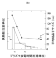
- FIG. 2 is a diagram showing the plasma discharge time dependence of the average crystallite size and the amount of foreign matter generated.
- FIG. 3 is a diagram showing the dependence of the average crystallite size, the ratio of high-temperature phase, and the amount of foreign matter generated on plasma discharge time.
- FIG. 4 is a diagram showing the correlation between the ratio of high-temperature phase and the amount of foreign matter generated by plasma discharge for a certain period of time.
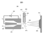
- FIG. 5 is a diagram schematically showing a manufacturing method for forming a film on the surface of the earth electrode shown in the embodiment of FIG. FIG.
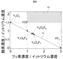
- FIG. 6 is a diagram showing the relationship among the compositions of yttrium oxyfluoride, yttrium fluoride, and yttrium oxide.
- FIG. 7 is a diagram showing a table comparing the characteristics of the film formed by the conventional technique and the film of this example.
- FIG. 1 is a vertical cross-sectional view schematically showing the configuration of a plasma processing apparatus according to an example.
- the plasma processing apparatus 100 of this embodiment is a plasma etching apparatus, and includes a vacuum vessel having a cylindrical part, a plasma forming part disposed above or around the cylindrical part so as to surround it, and a vacuum vessel having a cylindrical part.
- a vacuum evacuation section including a vacuum pump disposed below and evacuating the inside of the vacuum container is provided.
- a processing chamber 5, which is a space in which plasma is formed, is arranged inside the vacuum container and is configured to communicate with a vacuum exhaust section.
- the upper part of the processing chamber 5 is a space surrounded by a cylindrical inner wall, and constitutes a discharge chamber in which plasma 13 is formed.
- a stage 4 is arranged inside the processing chamber 5 below the discharge chamber where the plasma 13 is generated.
- the stage 4 is a sample table on which a wafer 3, which is a substrate to be processed, is placed and held.
- the plasma processing apparatus 100 can, for example, perform an etching process (hereinafter also simply referred to as a process) on a wafer 3, which is a substrate to be processed, placed on a stage 4.
- the stage 4 is composed of a cylindrical member with the vertical central axis of the stage 4 disposed at a position concentric with the discharge chamber or reasonably close to the discharge chamber when viewed from above.
- a space is provided between the bottom surface of the processing chamber 5 where an opening communicating with the vacuum evacuation section is arranged and the bottom surface of the stage 4, and a space is provided between the top and bottom surfaces of the processing chamber 5 in the vertical direction.
- the stage 4 is held at the position.
- the space inside the processing chamber 5 below the stage 4 is communicated with the discharge chamber through a gap between the side wall of the stage 4 and the cylindrical inner wall surface of the processing chamber 5 surrounding the stage 4.
- the stage 4 has a base material that is a metal member having a cylindrical shape.
- the base material of stage 4 includes a heater (not shown) placed inside a dielectric film placed to cover the top surface of the base material, and a heater (not shown) placed inside the base material concentrically around the central axis. Alternatively, multiple refrigerant channels (not shown) are arranged in a spiral manner.
- a heat conductive gas such as He is injected into the gap between the lower surface of the wafer 3 and the upper surface of the dielectric film. Supplied. For this reason, piping (not shown) through which a heat-conductive gas flows is arranged inside the base material and the dielectric film.
- the base material of the stage 4 is connected to a high frequency power source 12 to which high frequency power is supplied for forming an electric field for attracting charged particles in the plasma above the upper surface of the wafer 3 during processing of the wafer 3 by plasma.
- a high frequency power source 12 to which high frequency power is supplied for forming an electric field for attracting charged particles in the plasma above the upper surface of the wafer 3 during processing of the wafer 3 by plasma.
- an electrostatic force is generated inside the dielectric film and the wafer 3 to attract and hold the wafer 3 on the upper surface of the dielectric film.
- a membrane electrode (not shown) to which DC power is supplied is provided.
- Electrodes are arranged radially from the central axis in the vertical direction on the approximately circular upper surface of the wafer 3 or the stage 4 in multiple regions in a symmetrical manner around the central axis, and each of the multiple regions can be given a different polarity. It is composed of
- a window member 2 is provided above the upper surface of the stage 4 of the processing chamber 5.
- the window member 2 is arranged to face the upper surface of the stage 4 and constitutes the upper part of the vacuum container.
- the window member 2 has a disk shape made of a dielectric material such as quartz or ceramics and airtightly seals the inside and outside of the processing chamber 5 .
- a shower plate 1 is provided below the window member 2 at a position that constitutes the ceiling surface of the processing chamber 5 and is disposed with a gap 6 between the lower surface of the window member 2 and the ceiling surface of the processing chamber 5 .
- the shower plate 1 has a disk shape made of a dielectric material such as quartz and has a plurality of through holes 7 in its center.
- the gap 6 is connected to the vacuum container so as to communicate with the processing gas supply piping 25.
- a valve 26 that opens or closes the inside of the processing gas supply pipe 25 is arranged at a predetermined location of the processing gas supply pipe 25 .
- the flow rate or speed of the processing gas (processing gas) supplied into the processing chamber 5 is adjusted by a gas flow rate control means (not shown) connected to one end of the processing gas supply piping 25. 26 flows into the gap 6 through the open processing gas supply pipe 25.
- the processing gas that has flowed into the gap 6 is then diffused inside the gap 6 and is supplied into the processing chamber 5 from the upper side of the processing chamber 5 through the through hole 7 of the shower plate 1 .
- a vacuum evacuation section that exhausts gas and particles inside the processing chamber 5 is arranged below the vacuum container.
- the vacuum evacuation section is located directly below the stage 4 on the bottom of the processing chamber 7 and is provided inside the processing chamber 5 through an exhaust port, which is an opening for evacuation that is arranged so that the central axes in the vertical direction are approximately the same. emit gases and particles.
- the vacuum evacuation section includes a pressure adjustment plate 14 and a turbo molecular pump 10 that is a vacuum pump.
- the pressure adjustment plate 14 is a disk-shaped valve that moves up and down above the exhaust port to increase or decrease the area of the flow path through which gas flows into the exhaust port.
- the vacuum evacuation section further includes a dry pump 9, which is a roughing pump, and a valve 16.
- the outlet of the turbomolecular pump 10 is connected to and communicates with the dry pump 9 via an exhaust pipe.
- a valve 16 is arranged on the exhaust pipe.
- the pressure adjustment plate 14 also serves as a valve that opens and closes the exhaust port.
- the vacuum container is equipped with a pressure detector 27 that is a sensor for detecting the pressure inside the processing chamber 5.
- the signal output from the pressure detector 27 is transmitted to a control section (not shown), and the pressure value is detected.
- the pressure adjustment plate 14 is driven based on a command signal output from the control section in accordance with the value of the pressure. As a result, the vertical position of the pressure adjustment plate 14 changes, and the area of the exhaust flow path increases or decreases.
- valve 15 is a slow exhaust valve for slowly exhausting the processing chamber 5 from atmospheric pressure to vacuum using the dry pump 9.
- the valve 17 is a main exhaust valve for high-speed exhaust by the dry pump 9.
- a waveguide 19 and a magnetron oscillator 18 are arranged above and around the side wall of the upper cylindrical portion of the vacuum container constituting the processing chamber 5.
- the waveguide 19 and the magnetron oscillator 18 are configured to form an electric field or a magnetic field that is supplied to the processing chamber 5 to form plasma. That is, above the window member 2, a waveguide 19, which is a conduit through which the electric field of microwaves supplied to the inside of the processing chamber 5 propagates, is disposed, and one end of the waveguide 19 is arranged to oscillate the electric field of the microwave.
- a magnetron oscillator 18 is arranged to output the signal.
- the waveguide 19 includes a rectangular waveguide section and a circular waveguide section.
- the rectangular waveguide section has a rectangular vertical section, its axis extends in the horizontal direction, and the magnetron oscillator 18 is disposed at one end.
- the circular waveguide section is connected to the other end of the rectangular waveguide section, has a central axis extending in the vertical direction, and has a circular cross section.
- a hollow portion having a cylindrical shape with an increased diameter is disposed at the lower end of the circular waveguide portion.
- the cavity is configured such that the electric field of a particular mode is enhanced within the cavity.
- a multi-stage solenoid coil 20 and a solenoid coil 21 serving as magnetic field generating means are provided above and around the cavity and surrounding the side of the processing chamber 5 .
- an unprocessed wafer 3 is placed in a transfer chamber inside a vacuum transfer container, which is another vacuum container (not shown) connected to the side wall of the vacuum container.
- the substrate is placed on the tip of an arm of a vacuum transfer device (not shown) such as a robot arm, and is transferred into the processing chamber 5.
- the unprocessed wafer 3 at the tip of the arm is placed on the upper surface of the stage 4.
- the arm of the vacuum transfer device leaves the processing chamber 5, the inside of the processing chamber 5 is sealed.
- the unprocessed wafer 3 is held on the dielectric film by the electrostatic force generated by applying a DC voltage to the electrostatic adsorption electrode in the dielectric film of the stage 4.
- gas having heat transfer properties such as He is injected into the piping arranged inside the stage 4. supplied through.
- a refrigerant whose temperature is adjusted to a predetermined range by a refrigerant temperature regulator (not shown) is supplied to the refrigerant flow path inside the stage 4 . This promotes heat transfer between the temperature-adjusted substrate of the stage 4 and the wafer 3, and the temperature of the wafer 3 is adjusted to a temperature value within a range suitable for starting the process.
- the processing gas whose flow rate or speed is adjusted by the gas flow rate control means is supplied into the processing chamber 5 through the processing gas supply pipe 25 from the gap 6 through the through hole 7, and is processed from the exhaust port by the operation of the turbo molecular pump 10.
- the inside of the chamber 5 is evacuated, and due to the balance between the two (supply of processing gas to the inside of the processing chamber 5 and evacuation of the inside of the processing chamber 5), the pressure inside the processing chamber 5 is within a range suitable for processing. Adjusted to the pressure value. In this state, the microwave electric field oscillated by the magnetron oscillator 18 propagates inside the waveguide 19, passes through the window member 2 and the shower plate 1, and is radiated into the processing chamber 5.
- the magnetic field generated by the solenoid coils 20 and 21 is supplied to the processing chamber 5, and electron cyclotron resonance (ECR) is generated by the interaction between the magnetic field and the electric field of the microwave, and atoms or The molecules are excited, ionized, and dissociated to generate plasma 13 inside the processing chamber 5.
- ECR electron cyclotron resonance
- the plasma 13 When the plasma 13 is formed, high frequency power is supplied from the high frequency power supply 12 to the base material of the stage 4, a bias potential is formed above the upper surface of the wafer 3, and charged particles such as ions in the plasma 13 are transferred to the wafer. 3, the etching process of the target film layer of a film structure having a plurality of film layers including a target film layer and a mask layer formed in advance on the top surface of the wafer 3 is performed. , progresses along the pattern shape of the mask layer. When a detector (not shown) detects that the processing of the film layer to be processed has reached its end point, the supply of high-frequency power from the high-frequency power source 12 is stopped, the plasma 13 is extinguished, and the processing is stopped. Ru.
- control unit determines that there is no need to further proceed with the etching process of the wafer 3
- high vacuum evacuation is performed. Further, after the static electricity is removed and the wafer 3 is released from adsorption, the arm of the vacuum transfer device enters the processing chamber 5, and the processed wafer 3 is transferred to the arm. Thereafter, as the arm contracts, the wafer 3 is transferred to a vacuum transfer chamber outside the processing chamber 5.
- the inner wall surface of such a processing chamber 5 is a surface facing the plasma 13 and exposed to its particles.
- a member in the processing chamber 5 that functions as a grounding electrode facing and in contact with the plasma.
- the ground electrode 22 is arranged to cover the lower surface of the internal side wall (inner wall) of the processing chamber 5 surrounding the discharge chamber, with the purpose of functioning as a grounding electrode.
- the ground electrode 22 is constituted by a ring-shaped member disposed above the upper surface of the stage 4 so as to cover the lower surface of the inner wall of the processing chamber 5 surrounding the discharge chamber.
- the earth electrode 22 includes a base material made of a conductive material and a film covering the surface of the base material.
- the base material of the earth electrode is made of a metal such as a stainless steel alloy or an aluminum alloy.
- a coating 24 made of a material with high plasma resistance is disposed on the surface of the earth electrode 22 so as to cover the base material of the earth electrode 22.
- the coating 24 makes it possible to maintain the function of the ground electrode 22 covering the inner wall of the processing chamber 5 as an electrode through which plasma is transmitted, while suppressing damage caused by the plasma in the ground electrode 22 .
- the base material of the earth electrode 22 and the coating 24 disposed over the base material can be considered as internal members whose surfaces face the plasma.
- the coating 24 may also be referred to as a coating 24.
- the coating 24 may be a laminated film.
- the coating 24 is made of, for example, yttrium oxide (Y 2 O 3 ), yttrium fluoride (YF 3 ), yttrium oxyfluoride (YOF), or a material containing one or more of these by atmospheric plasma spraying, A ground electrode whose surface roughness is within a predetermined range using suspension plasma spraying, explosive spraying, reduced pressure plasma spraying, aerosol deposition (AD), or physical vapor deposition (PVD).
- the base material 23 of the inner wall of the processing chamber 5, which does not have the function of the earth electrode 22, is also made of metal such as stainless steel alloy or aluminum alloy.
- the surface of the base material 23 is also subjected to passivation treatment, various types of thermal spraying, PVD, chemical vapor deposition (CVD), etc. in order to suppress corrosion, metal contamination, and the generation of foreign substances caused by exposure to the plasma 13.
- the base material 23 is treated to improve its corrosion resistance against plasma and to reduce wear and tear on the base material 23.
- a ceramic material such as yttrium oxide or quartz is placed between the inner wall surface of the cylindrical base material 23 and the discharge chamber.
- a cylindrical cover (not shown) may be provided.
- the coating 24 of this example was produced based on the following knowledge.
- Patent Document 9 Japanese Unexamined Patent Publication No. 2019-192701 and Advances in X-ray analysis 50, pp. 197 (2019) (Non-Patent Document 1). As shown in Fig. 5, when the average crystallite size is increased, more foreign particles are generated on the semiconductor wafer in the plasma processing apparatus. For this reason, Patent Document 9 discloses a technique for suppressing the generation of foreign substances by reducing the crystallite size of the coating to 50 nm or less.
- FIG. 2 is a diagram showing the correlation between plasma discharge time, amount of foreign matter generated, and crystallite size.
- the bar graph shows the number of foreign particles generated when the film 24 was irradiated with plasma from time (t1) at the left end of the bar to time (t2) at the right end of the bar. Furthermore, the number of foreign particles detected per unit time is shown as a vertical axis on the left, and the time of plasma irradiation (center of the irradiation time) is shown as a horizontal axis, as shown in white squares ( ⁇ ). The child size is indicated by a black circle ( ⁇ ) on the right vertical axis.
- Figure 3 shows the results of examining the causes of foreign matter generation in a range where the average crystallite size is 40 nm or less. Even if the plasma exposure time (horizontal axis) is increased, the average crystallite size indicated by the black circle ( ⁇ ) (lower side of the right vertical axis) does not show a major change around 30 nm. . On the other hand, the amount of foreign matter generated per unit time (number of foreign matter: left vertical axis) indicated by the white square ( ⁇ ) decreases as the time of exposure to plasma (horizontal axis) increases.
- the ratio of rectangular or orthorhombic crystals, which are low-temperature phases, to the entire crystallites is increasing, as indicated by black diamonds ( ⁇ ).
- the ratio of this low-temperature phase is determined by the amount M1 (number, mass, or volume) of rectangular or orthorhombic crystals that are the low-temperature phase of the material constituting the film 24 and the amount M2 (number, mass, or volume) of hexagonal crystals that are the high-temperature phase.
- FIG. 4 is a diagram showing the correlation between the ratio of high-temperature phase and the amount of foreign matter generated by plasma discharge for a certain period of time.
- the horizontal axis represents the ratio of the low-temperature phase or high-temperature phase of the material containing yttrium constituting the film 24 on the surface of the ground electrode 22 of the wafer 3 processed by the plasma processing apparatus 100 according to the present embodiment, to the total.
- the number of foreign particles detected from the surface of the wafer 3 is plotted on the vertical axis.
- Patent Document 1 shows an example of a film having 100% rectangular crystals, but the crystal size of the material constituting the film is 1 ⁇ m or more.
- Patent Document 9 describes the temperature of the surface of a film when forming a film by plasma spraying under atmospheric pressure conditions using a material containing yttrium fluoride, as described in the examples and drawings of Patent Document 9.
- the ratio of rectangular crystals (orthorhombic crystals) which is a low-temperature phase, among the crystals in the film increases to 60% or higher, and the crystallite size increases. It has been shown that the thickness can be reduced to 50 nm or less.
- Patent Document 6 The Y 2 O 3 -ZrO 2 solid solution shown in Patent Document 6 is zirconia to which yttria is added to stabilize the high temperature phase, and is a material well known as yttria-stabilized zirconia. Furthermore, Non-Patent Document 2 describes academic research regarding yttrium fluoride stabilized zirconia (YF 3 -ZrO 2 ).
- the disclosers have discovered that the high-temperature hexagonal phase of the material constituting the film 24 undergoes a phase change to a low-temperature phase, rectangular or orthorhombic, at a specific temperature range (for example, room temperature around 25° C.). It was assumed that fine particles were generated due to the phase change of the crystal at this time, and it was thought that the generation of foreign matter could be suppressed by suppressing such phase change and stabilizing the high-temperature phase crystal. That is, by stabilizing the high-temperature phase and making it difficult for the high-temperature phase to change into a low-temperature phase during plasma discharge, it is expected that generation of foreign matter due to phase change can be prevented.
- a specific temperature range for example, room temperature around 25° C.
- Non-Patent Document 3 states that zirconia (ZrO 2 ) is stabilized by introducing Y 3+ ions, which have a lower valence than Zr 4+ ions, reducing the coordination number of Zr due to the oxygen ion vacancy effect, and by introducing Zr 4+ ions. It has been derived from first-principles calculations that the cause is lattice strain caused by introducing ions larger than the radius (80 pm).
- Patent Document 8 describes a technique for stabilizing or partially stabilizing the high-temperature phase of yttrium oxyfluoride by adding CaF 2 to yttrium oxide and yttrium fluoride and sintering the mixture. This suggests that the high-temperature phase can be stabilized by introducing Ca 2+ ions with a lower valence than Y 3+ and utilizing the vacancy effect of fluorine ions or oxygen ions. Further, Patent Document 7 describes that when Y 2 O 3 is added to yttrium-based fluoride, the high temperature phase is partially stabilized, the form of cracks changes, and surface cracks can be reduced.
- Fig. 1 shows that 15 mol% of yttrium oxide is dissolved in a yttrium fluoride melt at 1260°C.
- YF 3 is segregated at the grain boundaries of YOF particles. This indicates that in Y 2 O 3 -YF 3, YF 3 and YOF are eventually separated, and the molar ratio of YF 3 :YOF becomes 3:2. From this, it is considered that in Y 2 O 3 -YF 3 of Patent Document 7, YOF in YF 3 acts as a pinning site and stops the propagation of cracks.
- the main layer was Y 5 O 4 F 7 and contained 40% of the low temperature phase yttrium fluoride (YF 3 ) and the high temperature phases (yttrium oxyfluoride (YOF) and yttrium fluoride (YF 3 )).
- the crystallite size of Y 5 O 4 F 7 was 35 nm.
- the element concentrations of the film 24 were measured using fluorescent X-rays and were found to be Y: 32 at%, O: 9.4 at%, and F: 58 at%.
- the present inventors further investigated corrosion caused by oxidation and fluoride on the surface of the film 24 made of YOF and Y2O3 .
- Y2O3 on the surface of the film 24 is etched and fluorinated by being exposed to plasma discharge during the etching process of the wafer 3. Further, YF 3 in the film 24 is similarly oxidized.
- the film 24 exposed to the plasma is a mixed film of YOF, which corresponds to a molar ratio of Y 2 O 3 and YF 3 of 1:1, and Y 5 O 4 F 7 , which is a stable phase in the vicinity thereof.
- the YOF is also exposed to plasma discharge formed during processing of the wafer 3 for a long period of time, the surface thereof will be oxidized. From this, it is considered that if the Y:O molar ratio of the material constituting the coating 24 formed by thermal spraying is 1:1.5 or more, it will be difficult to oxidize even when exposed to plasma for a long period of time.
- F it is believed that fluorination when exposed to plasma is suppressed when the molar ratio of Y:F in the material of the film 24 is 1:1 or more, preferably 1:1.4 or more. It will be done.
- Patent Document 8 in order to (at least partially) stabilize the high-temperature phase of yttrium oxyfluoride, Ca2 + ions having a lower valence than Y3+ ions are introduced into the YOF crystal by adding CaF2 . . Therefore, it is assumed that the high temperature phase is stabilized by the oxygen or fluorine ion vacancy effect. However, the generation of oxygen ion or fluorine ion vacancies reduces the resistance to oxygen plasma or fluorine plasma.
- the concentration of elements although fluorine increases, oxygen does not increase, so even if the Y:F molar ratio becomes 1:1 or more, the Y:O molar ratio does not become 1:1.5 or more. For this reason, if the film 24 made of a material obtained by adding CaF 2 to YOF is exposed to plasma for a long time, oxidation will progress on the surface of the film 24, and there is a possibility that foreign matter will be generated.
- the present inventors considered stabilizing the film 24 by introducing ions larger than the ionic radius (93 pm) of Y 3+ into the YOF crystal through the lattice strain effect.
- Elements with an ionic radius greater than 93 pm that are divalent or higher ions are limited to Ce 3+ at 101 pm, Ca 2+ at 99 pm, and Sr 2+ at 113 pm.
- the coating 24 can be formed using a thermal spraying method using atmospheric plasma (atmospheric plasma spraying, APS).
- the coating 24 is formed using an atmospheric plasma spraying method, using a CeO 2 -YOF solid solution as a material, and forming plasma using a gas toward the base material to be coated under atmospheric pressure or a pressure close to atmospheric pressure.
- the coating 24 can be formed by supplying particles of the material of the coating 24 into plasma, melting the particles, and spraying the coating onto the surface of the base material to form a layer.
- FIG. 5 is a diagram schematically showing a manufacturing method for forming a film on the surface of the earth electrode shown in the embodiment of FIG.
- a thermal spray gun GN is placed at a distance from the surface of the base material 23, and the gas blown from the gun GN toward the top surface of the base material 23 is used to inject into the formed plasma.
- the fine particles are made into a molten or semi-molten state, and the fine particles are sprayed onto the upper surface of the base material 23 along the direction in which the plasma flows. be.
- the thermal spraying gun GN is composed of a power source 203, a nozzle 201, and a material supply pipe 205.
- the nozzle 201 is electrically connected to a power source 203, and a predetermined voltage is applied from the power source 203. Further, the nozzle 201 is configured to blow out argon (Ar) gas (GA) for plasma formation from an opening OP1 at the tip.
- the material supply pipe 205 is arranged at a predetermined distance from the opening OP1 at the tip of the nozzle 201.
- the material supply pipe 205 is configured so that fine particles of the material are blown out from the opening OP2 at its tip in a direction transverse to the flow direction 202 of the argon gas GA.
- a rod-shaped terminal T1 at the center and a cylindrical terminal T2 at the outer periphery surrounding the outer periphery of the terminal T1 with a gap are electrically connected to respective polar terminals of the power source 203.
- a gap on the outer periphery of the central terminal T1 is communicated with an opening OP1 of a gas outlet at the tip of the nozzle 201, and forms a gas supply path for the argon gas GA.
- the direction of the axis passing through the gas outlet opening OP1 from the gas supply path of the argon gas GA is in the direction of the blowout of the argon gas GA from the tip of the nozzle 201 or the direction of radiation of plasma formed beyond the tip of the nozzle 201. It's in line.
- the configuration is such that arc discharge is generated in the space beyond the outlet (OP1) by high voltage applied from the power source 203 to each terminal T1, T2 of the nozzle 201.
- Ar gas GA supplied to the gas supply path from a gas source (not shown) connected to the nozzle 201 is discharged from the gas outlet (OP1) as a gas flow 202 toward the upper surface of the base material 23.
- a high voltage is applied from the power supply 203 to each terminal T1, T2 to generate an arc discharge in the space beyond the outlet (OP1).
- the generated arc discharge excites Ar gas, and a thermal spray frame 204 is formed between the nozzle 201 and the base material 23.
- the thermal spray material 206 passes through the flow path inside the material supply pipe 205 together with the flow 207 of the transport gas, and is directed toward the thermal spray frame 204 from the opening OP2 at the tip of the material supply pipe 205.
- the thermal spray material 206 is fine particles of the material of the coating 24 in which the ratio of CeO 2 to yttrium oxyfluoride is adjusted to be 35 mol % or a value close to this.
- Each particle constituting the thermal spraying material 206 is in a molten or semi-molten state, and along the plasma of the thermal spraying flame 204 and the flow 202 of Ar gas GA, the particles constituting the thermal spraying material 206 are exposed to the surface of the base material 23 made of a material containing aluminum or an aluminum alloy. collides with and adheres to.
- Each particle constituting the adhered thermal spray material 206 is solidified on the surface of the base material 23 as it cools.
- the solidified and mutually welded particles cover a predetermined region of the surface of the base material 23 and are stacked upward until a desired thickness is reached, forming a coating 208 (24). In this example, this was repeated to form a film 24 with a thickness of about 100 ⁇ m.
- the distance between the nozzle 201 and the base material 23 is set so that semi-molten particles do not remain inside the coating 24 when the coating 208 (24) is formed to a desired thickness.
- the coatings 24 according to the examples described below are all formed using atmospheric plasma spraying as shown in FIG.
- Ca and Sr become divalent positive ions, there is a risk of contaminating the semiconductor wafer, and it is not appropriate to add too much.
- the concentration of each element in the film 24 thus formed was measured using fluorescent X-rays. As a result, on the surface of the film 24, Y: 20 at%, O: 45 at%, F: 22 at%, and Ce: 13 at%. Further, it was detected that Y:O was 1:2.2 and Y:F was 1:1.1.
- the results of crystal structure analysis by XRD revealed that the main layer was YOF (CeO 2 -YOF solid solution) and that trace amounts of YF 3 and CeO 2 crystals were present. Further, the crystallite size of YOF was 40 nm, and the hexagonal crystal ratio of the CeO 2 -YOF solid solution was about 90%. On the other hand, as a result of analyzing the crystal structure of the film 24 exposed to plasma for a long time, almost no change was observed in the hexagonal phase ratio compared to that of the film not exposed to plasma.
- Yttrium oxyfluoride has a hexagonal crystal in its high-temperature phase and a rectangular crystal in its low-temperature phase, but it is not clear whether the hexagonal crystal can be used as a high-temperature phase when stabilized, so it is described as hexagonal or rectangular rather than high-temperature phase or low-temperature phase. .
- the above-mentioned yttrium oxyfluoride is composed of Y 3+ , O 2 ⁇ and F ⁇ . Since the only positive ion is Y 3+ , in order to increase the concentration (molar ratio) of oxygen in the film 24, Y 5 O 6 F 3, etc., in which 2F ⁇ and O 2 ⁇ are exchanged, is also considered, but for Y Therefore, it is not possible to increase the concentration of both O and F. Therefore, the present inventors investigated a method of increasing the oxygen concentration by adding positive ions of an element different from Y.
- YFSeO 3 , YFCO 3 , YFSO 4 , YFMoO 4 , YF(OH) 2 and the like were investigated as stable structures in which YOF has an additional element.
- the ionic radii of the elements added to these materials are Se 6+ : 42 pm, C 4+ : 15 pm, S 6+ : 29 pm, Mo 6+ : 62 pm, which are smaller than the ionic radius of Y 3+ (93 pm).
- the disclosers added an element M that becomes a positive ion with the ionic radius of Y 3+ or less to the YOF material, increasing the oxygen concentration to 1.5 times or more and the fluorine concentration to 1 times or more than Y.
- Element M is an ion with a valence of +4 or +6, and must have an ionic radius smaller than that of Y 3+ .
- C 4+ , Si 4+ , Ge 4+ , Zr 4+ , Hf 4+ , S 6+ , Cr 6+ , Se 6+ , Mo 6+ , Te 6+ , and W 6+ are candidates.
- Sn and Pb were excluded because their divalent ionic radii were larger than Y 3+ .
- the element M which has a valence of 1 to 2, was excluded because it is highly likely to become an element that causes semiconductor contamination. That is, the element M that becomes a +4-valent or +6-valent ion is at least one of C, Si, Ge, Zr, Hf, S, Cr, Se, Mo, Te, and W.
- the film 24 of this example was formed from yttrium oxyfluoride and an oxide of the elements M, Y, and F by thermal spraying using atmospheric plasma in the same manner as in the above study. That is, in this example, the spray flame formed by applying a high voltage to the nozzle and causing discharge while flowing argon gas as a plasma gas contains particles of yttrium oxyfluoride and YFCO 3 whose element M is C (carbon). Particles of the material were introduced into a thermal spray flame along with a transport gas, and the molten particles were emitted onto the surface of the base material of the ground electrode 22 to form a coating 24 .
- a film 24 was formed using YFSO 4 in which the element M is S as a material added to yttrium oxyfluoride, and the concentration of the elements was similarly detected by fluorescent X-ray measurement.
- XRD crystal structure analysis by XRD, it was found that the main layer is YOF, a trace amount of YFSO4 is present, the crystallite size of YOF is 40 nm, and the ratio of hexagonal crystals to the whole is about 90%. Ta. Furthermore, even after long-term exposure to plasma, no significant changes were observed in the hexagonal phase ratio or oxygen concentration from those before exposure.
- the film 24 can be similarly formed using YFSeO 3 and YFMoO 4 in which Se and Mo are used as the element M.
- the coating 24 may be formed using a suspension plasma spray process.
- a high voltage is applied to the terminals at the center and outer periphery of the nozzle 201 under conditions of atmospheric pressure to generate an arc discharge, and the supplied Ar gas is A material in which particles of a material containing yttrium oxyfluoride and YFMoO 4 particles are suspended in a solvent is introduced into the thermal spray flame 204 generated by plasma, and the surface of the base material 23 of the earth electrode 22 is The film 24 is formed by irradiating and adhering to and covering.
- the thermal spraying temperature is set high so that the solvent is vaporized by heating in the thermal spraying frame 204 and particles of the thermal spraying material 206 do not remain in the coating 24 in a semi-molten state, and the nozzle 203 and the upper surface of the base material 23 are The distance between the two is set to a value within a predetermined range.
- Yttrium oxyfluoride, YFCO 3 , YFSO 4 , and YFSeO 3 may be used as materials for forming the film 24 .
- the concentrations of elements in the film 24 detected in the same manner as above are Y: 20 at%, O: 50 at%, F: 20 at%, Mo: 10 at%, Y:O is 1:2.5, Y:F
- the ratio was 1:1.
- the main layer is YOF
- the crystallite size of YOF is 33 nm
- the hexagonal phase ratio is about 70%, and even when exposed to plasma for a long time, there is no significant change in the hexagonal phase ratio. It was found that no change was observed.
- thermal spraying materials that can be used include yttrium oxyfluoride, yttrium fluoride particles, and silicon dioxide powder suspended in a solvent.
- concentrations of the elements in the film 24 thus formed are Y: 20 at%, O: 40 at%, F: 28 at%, and Si: 12 at%, with Y:O being 1:2 and Y:F being 1:1. It was confirmed that the value was .4.
- the main layer of the film 24 was Y 5 O 4 F 7 and also contained YOF (SiO 2 -Y 5 O 4 F 7 , SiO 2 - (considered to be YOF).
- the crystallite size of Y 5 O 4 F 7 was 30 nm, and the proportion of hexagonal crystals was approximately 80%, and no significant change was observed in the phase proportion of hexagonal crystals even after long-term exposure to plasma.
- silicon oxide germanium oxide, hafnium oxide, sulfur oxide, selenium oxide, chromium oxide, molybdenum oxide, tellurium oxide, and tungsten oxide can be used.
- the film 24 was formed using PVD.
- a sintered material of yttrium oxyfluoride was used as the PVD target, and a chip of yttria-stabilized zirconia was placed on it to form a film.
- the concentrations of the elements in the film 24 are Y: 25 at%, O: 42 at%, F: 28 at%, Zr: 5 at%, Y:O: 1:1.7, Y:F: 1: It turned out to be 1.1.
- the main layer of the film 24 was Y 5 O 4 F 7 , and Y 2 O 3 and ZrO 2 were not detected.
- the crystallite size of Y 5 O 4 F 7 was 40 nm, and the hexagonal crystal ratio was about 25%. No significant change was detected in the hexagonal and rectangular (tetragonal) phase ratios after long-term exposure to plasma compared to those before exposure.
- the film 24 was formed using a mixture of a fine powder obtained by crushing a sintered material of yttrium oxyfluoride and a fine powder obtained by crushing YFCO 3 and compression-molding the mixture as a PVD target.
- YFSeO 3 , YFSO 4 , YFMoO 4 can be used instead of YFCO 3 .
- the concentration of elements in the film 24 is Y: 25 at%, O: 50 at%, F: 25 at%, and C: 25 at%, with Y:O being 1:2 and Y:F being 1:1.
- Y:O being 1:2 and Y:F being 1:1.
- the film 24 is a mixture of YOF and Y(CO 3 )F crystals, and the crystallite size of YOF is 38 nm, and the hexagonal crystal ratio is approximately 100%. It turned out to be. Further, even when exposed to plasma for a long time, no significant change was observed in the hexagonal phase ratio from before exposure.
- Figure 6 shows the relationship among the compositions of yttrium oxyfluoride, yttrium fluoride, and yttrium oxide.
- the range of this embodiment corresponds to the shaded area 60, which cannot be achieved using only conventional techniques such as yttrium oxyfluoride, yttrium fluoride, and yttrium oxide.
- Y 2 O 3 crystals are not oxidized even when subjected to oxygen plasma treatment. This is because chemically more than 1.5 times more oxygen than yttrium cannot be combined with yttrium. In order to bind more than 1.5 times as much oxygen as yttrium, the presence of the element M with a positive valence is essential. Further, when a Y 2 O 3 crystal is subjected to fluorine plasma treatment, it becomes YOF to Y 5 O 4 F 7 with a Y:F ratio in the range of 1:1 to 1:1.4. The Y:O ratio at this time is 1:1 to 1:0.8.
- oxygen When accompanied by hydrogen reduction treatment such as HF gas plasma treatment, oxygen may be removed and become YF3 , but as can be seen in Figure 6, as F increases, O decreases, so the molar ratio Y:O ⁇ 1 :1.5, Y:F ⁇ 1:1 are not compatible.
- the inner wall material generally called YOF film is made of Y 2 O 3 , YF 3 , Y 5 O 4 F 7 , Y 6 O 5 F 8 , Y 6 O 6 F 9 or a mixture thereof. .
- These are all materials that exist on the line segment 61 shown in FIG. 6, so no matter what ratio these materials are mixed, the molar ratio as an average of the entire YOF that is the resulting material never deviates from above the line segment 61 in FIG. Therefore, in any case where the wafer 3 is processed by plasma using a gas containing oxygen or plasma using a gas containing fluorine in the processing chamber 5, the material constituting the film 24 on the surface of the ground electrode 22 is The composition of YOF lies on line segment 61 in FIG.
- composition of the film 24 According to the inventors' examination of the composition of the film 24 under multiple conditions, it was detected that the film 24 was slightly deviated from above the line segment 61; The composition of the YOF that made up the film 24 before the treatment was determined to be due to the influence of It was determined that it was above the line segment 61 in FIG. In other words, although the composition of the material of the three elements Y-O-F of the film 24 due to exposure to plasma is along the line segment 61 in FIG. It is considered that the material of the film 24 may not be along the line segment 61 in FIG. 6 due to the influence of reaction products and the like accompanying the treatment in step 3.
- the concentration ratio of oxygen and fluorine in the inner wall material is moved from the line 61 in FIG.
- the plasma resistance is improved.
- FIG. 7 is a diagram showing a table comparing the characteristics of the film formed by the conventional technique and the film 24 of this example.
- Table TAB shown in FIG. 7 shows the qualitative superiority or inferiority of the characteristics of the film formed by the conventional technique and the film 24 of this example in four stages ( ⁇ , ⁇ , ⁇ , ⁇ ).
- Table TAB shown in FIG. 7 shows the qualitative superiority or inferiority of the characteristics of the film formed by the conventional technique and the film 24 of this example in four stages ( ⁇ , ⁇ , ⁇ , ⁇ ).
- Table TAB shown in FIG. 7 shows the qualitative superiority or inferiority of the characteristics of the film formed by the conventional technique and the film 24 of this example in four stages ( ⁇ , ⁇ , ⁇ , ⁇ ).
- the material of the inner wall material is, as a typical example, yttrium oxyfluoride (YOF) and an element M (C, Si, Ge, Zr, Hf, S, Cr, Se, Mo, Te, W) oxide, fluoride, or fluorinated oxide (CeO 2 , YFCO 3 , YFSO 4 , YFSeO 3 , YFMoO 4 , or , SiO 2 ).
- YOF yttrium oxyfluoride
- element M C, Si, Ge, Zr, Hf, S, Cr, Se, Mo, Te, W
- fluoride or fluorinated oxide
- SiO 2 fluorinated oxide
- the element M is absent, absent, Ca, and the inner wall material is Y 2 O 3 , YF 3 , YOF, YF 3 +CaF 3 .
- the element M is Ce, C, S, Se, Mo, or Si
- the inner wall material is YOF+CeO 2 , YOF+YFCO 3 , YOF+YFSO 4 , YOF+YFSeO 3 , YOF+YFMoO 4 , YOF+SiO 2 . It is a part.
- the film 24 of this example is rated ⁇ or ⁇ in each property of oxidation property, fluoride resistance, and foreign matter generation, and is excellent compared to each property of the film of the conventional technology. It can be considered to have certain characteristics.
- the film 24 contains at least one of yttrium oxide, yttrium fluoride, and yttrium oxyfluoride, and an element that becomes a +4- or +6-valent ion with a smaller ionic radius than a +3-valent yttrium ion, and contains oxygen on average.
- the film is made of a material containing fluorine at a molar ratio of 1.5 times or more that of yttrium, and fluorine at a molar ratio of at least 1 time, preferably 1.4 times or more, that of yttrium.
- the material of the inner wall material constituting the film 24 is at least one of yttrium oxide, yttrium fluoride, and yttrium oxyfluoride, and an oxide or fluoride of the element M that becomes a +4- or +6-valent ion. It is a material containing a fluorinated oxy compound.
- Yttrium oxide, yttrium fluoride, and yttrium oxyfluoride are at least one of Y2O3 , YF3 , YOF, and Y5O4F7 .
- the oxide, fluoride, or fluoride oxide of the element M that becomes a +4-valent or +6-valent ion is any one of YFCO 3 , YFSeO 3 , YFSO 4 , and YFMoO 4 .
- the present disclosure is applicable to a plasma processing apparatus that processes a sample to be processed such as a semiconductor wafer, an internal member of the plasma processing apparatus, and a method of manufacturing the internal member of the plasma processing apparatus.
Landscapes
- Chemical & Material Sciences (AREA)
- Engineering & Computer Science (AREA)
- Materials Engineering (AREA)
- Organic Chemistry (AREA)
- Plasma & Fusion (AREA)
- Physics & Mathematics (AREA)
- Analytical Chemistry (AREA)
- Mechanical Engineering (AREA)
- Metallurgy (AREA)
- Chemical Kinetics & Catalysis (AREA)
- General Chemical & Material Sciences (AREA)
- Ceramic Engineering (AREA)
- Manufacturing & Machinery (AREA)
- Structural Engineering (AREA)
- Drying Of Semiconductors (AREA)
Abstract
Description
Claims (15)
- 真空容器内部に配置され、内側でプラズマが形成される処理室と、
前記処理室内に配置され、表面が前記プラズマに面する部材と、を備え、
前記部材は、その表面に、酸化イットリウム、フッ化イットリウム、オキシフッ化イットリウムの少なくとも1つと、+3価のイットリウムイオンよりもイオン半径が小さい+4価または+6価のイオンとなる元素とを含む材料から構成された皮膜であって、平均として酸素をイットリウムの1.5倍以上のモル比で、フッ素を前記イットリウムの1倍以上、好ましくは1.4倍以上のモル比で含む前記材料から構成された皮膜を備えた、プラズマ処理装置。 - 前記+4価または+6価のイオンとなる元素が、C、Si、Ge、Zr、Hf、S、Cr、Se、Mo、Te、Wの少なくとも何れか1つである、請求項1に記載のプラズマ処理装置。
- 前記酸化イットリウム、前記フッ化イットリウム、前記オキシフッ化イットリウムの少なくとも1つと、前記+4価または+6価のイオンとなる元素の酸化物、または、フッ化物、または、フッ化オキシ物との材料を溶射して、前記皮膜を形成する、請求項1または2に記載のプラズマ処理装置。
- 前記酸化イットリウム、フッ化イットリウム、オキシフッ化イットリウムが、Y2O3、YF3、YOF、Y5O4F7の少なくとも1つを含んだものであって、前記+4価または+6価のイオンとなる元素の前記酸化物、または、前記フッ化物、または、前記フッ化オキシ物が、YFCO3、YFSeO3、YFSO4、YFMoO4の何れか1つを含む、請求項3に記載のプラズマ処理装置。
- 前記皮膜の結晶の大きさの平均値が50nm以下である、請求項1または2に記載のプラズマ処理装置。
- 真空容器内部に配置され、その内側でプラズマが形成される処理室を有し、
前記処理室の内側に配置され、その表面が前記プラズマに面する内部部材であって、
前記内部部材の表面に、酸化イットリウム、フッ化イットリウム、オキシフッ化イットリウムの少なくとも1つと、+3価のイットリウムイオンよりもイオン半径が小さい+4価または+6価のイオンとなる元素とを含む材料から構成された皮膜であって、平均として酸素をイットリウムの1.5倍以上のモル比で、フッ素を前記イットリウムの1倍以上、好ましくは1.4倍以上のモル比で含む前記材料から構成された皮膜を備えた、プラズマ処理装置の内部部材。 - 前記+4価または+6価のイオンとなる元素が、C、Si、Ge、Zr、Hf、S、Cr、Se、Mo、Te、Wの少なくとも何れか1つである、請求項6に記載のプラズマ処理装置の内部部材。
- 前記酸化イットリウム、前記フッ化イットリウム、前記オキシフッ化イットリウムの少なくとも1つと、前記+4価または+6価のイオンとなる元素の酸化物、または、フッ化物、または、フッ化オキシ物との材料を溶射して、前記皮膜を形成する、請求項6または7に記載のプラズマ処理装置の内部部材。
- 前記酸化イットリウム、フッ化イットリウム、オキシフッ化イットリウムが、Y2O3、YF3、YOF、Y5O4F7の少なくとも1つを含んだものであって、前記+4価または+6価のイオンとなる元素の前記酸化物、または、前記フッ化物、または、前記フッ化オキシ物が、YFCO3、YFSeO3、YFSO4、YFMoO4の何れか1つを含む、請求項8に記載のプラズマ処理装置の内部部材。
- 前記皮膜の結晶の大きさの平均値が50nm以下である、請求項6または7に記載のプラズマ処理装置の内部部材。
- 真空容器内部に配置され、内側でプラズマが形成される処理室内に配置され、その表面が前記プラズマに面する内部部材であって、
前記内部部材の表面に、酸化イットリウム、フッ化イットリウム、オキシフッ化イットリウムの少なくとも1つと、+3価のイットリウムイオンよりもイオン半径が小さい+4価または+6価のイオンとなる元素とを含む材料を、大気圧でプラズマを用いて溶射して、平均として酸素をイットリウムの1.5倍以上のモル比で、フッ素を前記イットリウムの1倍以上、好ましくは1.4倍以上のモル比で含む前記材料から構成された皮膜を形成する、プラズマ処理装置の内部部材の製造方法。 - 前記+4価または+6価のイオンとなる元素が、C、Si、Ge、Zr、Hf、S、Cr、Se、Mo、Te、Wの少なくとも何れか1つである、請求項11に記載のプラズマ処理装置の内部部材の製造方法。
- 前記酸化イットリウム、前記フッ化イットリウム、前記オキシフッ化イットリウムの少なくとも1つと、前記+4価または+6価のイオンとなる元素の酸化物、または、フッ化物、または、フッ化オキシ物とを含む材料を溶射して、前記皮膜を形成する、請求項11または12に記載のプラズマ処理装置の内部部材の製造方法。
- 前記酸化イットリウム、フッ化イットリウム、オキシフッ化イットリウムが、Y2O3、YF3、YOF、Y5O4F7の少なくとも1つを含んだものであって、前記+4価または+6価のイオンとなる元素の前記酸化物、または、前記フッ化物、または、前記フッ化オキシ物がYFCO3、YFSeO3、YFSO4、YFMoO4の何れか1つを含む、請求項13に記載のプラズマ処理装置の内部部材の製造方法。
- 前記皮膜の結晶の大きさの平均値が50nm以下である、請求項11または12に記載のプラズマ処理装置の内部部材の製造方法。
Priority Applications (6)
| Application Number | Priority Date | Filing Date | Title |
|---|---|---|---|
| KR1020237027116A KR20240032700A (ko) | 2022-08-30 | 2022-08-30 | 플라스마 처리 장치, 플라스마 처리 장치의 내부 부재, 및 플라스마 처리 장치의 내부 부재의 제조 방법 |
| US18/280,354 US20250357087A1 (en) | 2022-08-30 | 2022-08-30 | Manufacturing method of inner member of plasma processing apparatus |
| PCT/JP2022/032583 WO2024047746A1 (ja) | 2022-08-30 | 2022-08-30 | プラズマ処理装置、プラズマ処理装置の内部部材、および、プラズマ処理装置の内部部材の製造方法 |
| CN202280014678.8A CN117957641A (zh) | 2022-08-30 | 2022-08-30 | 等离子处理装置、等离子处理装置的内部构件以及等离子处理装置的内部构件的制造方法 |
| JP2023544620A JP7607141B2 (ja) | 2022-08-30 | 2022-08-30 | プラズマ処理装置、プラズマ処理装置の内部部材、および、プラズマ処理装置の内部部材の製造方法 |
| TW112129759A TW202410741A (zh) | 2022-08-30 | 2023-08-08 | 電漿處理裝置、電漿處理裝置之內部構件及電漿處理裝置之內部構件之製造方法 |
Applications Claiming Priority (1)
| Application Number | Priority Date | Filing Date | Title |
|---|---|---|---|
| PCT/JP2022/032583 WO2024047746A1 (ja) | 2022-08-30 | 2022-08-30 | プラズマ処理装置、プラズマ処理装置の内部部材、および、プラズマ処理装置の内部部材の製造方法 |
Publications (1)
| Publication Number | Publication Date |
|---|---|
| WO2024047746A1 true WO2024047746A1 (ja) | 2024-03-07 |
Family
ID=90099158
Family Applications (1)
| Application Number | Title | Priority Date | Filing Date |
|---|---|---|---|
| PCT/JP2022/032583 Ceased WO2024047746A1 (ja) | 2022-08-30 | 2022-08-30 | プラズマ処理装置、プラズマ処理装置の内部部材、および、プラズマ処理装置の内部部材の製造方法 |
Country Status (6)
| Country | Link |
|---|---|
| US (1) | US20250357087A1 (ja) |
| JP (1) | JP7607141B2 (ja) |
| KR (1) | KR20240032700A (ja) |
| CN (1) | CN117957641A (ja) |
| TW (1) | TW202410741A (ja) |
| WO (1) | WO2024047746A1 (ja) |
Cited By (1)
| Publication number | Priority date | Publication date | Assignee | Title |
|---|---|---|---|---|
| WO2026014507A1 (ja) * | 2024-07-10 | 2026-01-15 | 住友大阪セメント株式会社 | 静電チャック部材及び静電チャック装置 |
Citations (5)
| Publication number | Priority date | Publication date | Assignee | Title |
|---|---|---|---|---|
| JP2016089241A (ja) * | 2014-11-08 | 2016-05-23 | リバストン工業株式会社 | 皮膜付き基材、その製造方法、その皮膜付き基材を含む半導体製造装置部材 |
| JP2018190985A (ja) * | 2017-05-10 | 2018-11-29 | アプライド マテリアルズ インコーポレイテッドApplied Materials,Incorporated | チャンバコンポーネント用金属オキシフッ化物膜 |
| JP2019192701A (ja) * | 2018-04-20 | 2019-10-31 | 株式会社日立ハイテクノロジーズ | プラズマ処理装置およびプラズマ処理装置用部材 |
| JP2020511388A (ja) * | 2017-03-06 | 2020-04-16 | アプライド マテリアルズ インコーポレイテッドApplied Materials,Incorporated | ホットプレスにより形成された焼結セラミック保護層 |
| WO2021124996A1 (ja) * | 2019-12-18 | 2021-06-24 | 信越化学工業株式会社 | フッ化イットリウム系溶射皮膜、溶射部材、及びフッ化イットリウム系溶射皮膜の製造方法 |
Family Cites Families (8)
| Publication number | Priority date | Publication date | Assignee | Title |
|---|---|---|---|---|
| JP3894313B2 (ja) | 2002-12-19 | 2007-03-22 | 信越化学工業株式会社 | フッ化物含有膜、被覆部材及びフッ化物含有膜の形成方法 |
| JP2009176787A (ja) | 2008-01-22 | 2009-08-06 | Hitachi High-Technologies Corp | エッチング処理装置及びエッチング処理室用部材 |
| JP5578383B2 (ja) | 2012-12-28 | 2014-08-27 | Toto株式会社 | 耐プラズマ性部材 |
| US20150079370A1 (en) | 2013-09-18 | 2015-03-19 | Applied Materials, Inc. | Coating architecture for plasma sprayed chamber components |
| JP5888458B2 (ja) | 2014-06-26 | 2016-03-22 | Toto株式会社 | 耐プラズマ性部材及びその製造方法 |
| US10280091B2 (en) | 2015-09-07 | 2019-05-07 | Mitsui Mining & Smelting Co., Ltd. | Yttrium oxyfluoride, starting material powder for production of stabilized yttrium oxyfluoride, and method for producing stabilized yttrium oxyfluoride |
| JP6443380B2 (ja) | 2016-04-12 | 2018-12-26 | 信越化学工業株式会社 | イットリウム系フッ化物溶射皮膜、及び該溶射皮膜を含む耐食性皮膜 |
| TWI663142B (zh) | 2016-11-10 | 2019-06-21 | Toto股份有限公司 | 結構物 |
-
2022
- 2022-08-30 CN CN202280014678.8A patent/CN117957641A/zh active Pending
- 2022-08-30 WO PCT/JP2022/032583 patent/WO2024047746A1/ja not_active Ceased
- 2022-08-30 US US18/280,354 patent/US20250357087A1/en active Pending
- 2022-08-30 JP JP2023544620A patent/JP7607141B2/ja active Active
- 2022-08-30 KR KR1020237027116A patent/KR20240032700A/ko not_active Ceased
-
2023
- 2023-08-08 TW TW112129759A patent/TW202410741A/zh unknown
Patent Citations (5)
| Publication number | Priority date | Publication date | Assignee | Title |
|---|---|---|---|---|
| JP2016089241A (ja) * | 2014-11-08 | 2016-05-23 | リバストン工業株式会社 | 皮膜付き基材、その製造方法、その皮膜付き基材を含む半導体製造装置部材 |
| JP2020511388A (ja) * | 2017-03-06 | 2020-04-16 | アプライド マテリアルズ インコーポレイテッドApplied Materials,Incorporated | ホットプレスにより形成された焼結セラミック保護層 |
| JP2018190985A (ja) * | 2017-05-10 | 2018-11-29 | アプライド マテリアルズ インコーポレイテッドApplied Materials,Incorporated | チャンバコンポーネント用金属オキシフッ化物膜 |
| JP2019192701A (ja) * | 2018-04-20 | 2019-10-31 | 株式会社日立ハイテクノロジーズ | プラズマ処理装置およびプラズマ処理装置用部材 |
| WO2021124996A1 (ja) * | 2019-12-18 | 2021-06-24 | 信越化学工業株式会社 | フッ化イットリウム系溶射皮膜、溶射部材、及びフッ化イットリウム系溶射皮膜の製造方法 |
Cited By (1)
| Publication number | Priority date | Publication date | Assignee | Title |
|---|---|---|---|---|
| WO2026014507A1 (ja) * | 2024-07-10 | 2026-01-15 | 住友大阪セメント株式会社 | 静電チャック部材及び静電チャック装置 |
Also Published As
| Publication number | Publication date |
|---|---|
| TW202410741A (zh) | 2024-03-01 |
| CN117957641A (zh) | 2024-04-30 |
| US20250357087A1 (en) | 2025-11-20 |
| JPWO2024047746A1 (ja) | 2024-03-07 |
| KR20240032700A (ko) | 2024-03-12 |
| JP7607141B2 (ja) | 2024-12-26 |
Similar Documents
| Publication | Publication Date | Title |
|---|---|---|
| US12494348B2 (en) | Plasma processing apparatus and member of plasma processing chamber | |
| US7955513B2 (en) | Apparatus and method for reactive atom plasma processing for material deposition | |
| US5895586A (en) | Plasma processing apparatus and plasma processing method in which a part of the processing chamber is formed using a pre-fluorinated material of aluminum | |
| Lindfors et al. | Cathodic arc deposition technology | |
| EP1300877A1 (en) | Plasma processing device | |
| CN101302610A (zh) | 具有覆盖钇铝层的部件的处理腔 | |
| US20110284365A1 (en) | Lanthanoid aluminate film fabrication method | |
| JP7607141B2 (ja) | プラズマ処理装置、プラズマ処理装置の内部部材、および、プラズマ処理装置の内部部材の製造方法 | |
| JP4181069B2 (ja) | プラズマ処理装置 | |
| CN114277340B (zh) | 零部件、耐等离子体涂层的形成方法和等离子体反应装置 | |
| JP3986513B2 (ja) | 薄膜形成装置 | |
| JPH03204925A (ja) | プラズマプロセス用装置および方法 | |
| TWI523972B (zh) | Plasma processing apparatus and method | |
| TW202037737A (zh) | 電漿處理裝置及電漿處理裝置之內部構件以及該內部構件之製造方法 | |
| CN114678248B (zh) | 形成涂层的装置和方法、零部件和等离子体装置 | |
| JP7847217B2 (ja) | プラズマ処理装置用部材の製造方法 | |
| JP6883274B2 (ja) | 金属酸化物薄膜の製造方法及び薄膜製造装置 | |
| JPH04128393A (ja) | ラジカル反応による無歪精密加工装置 | |
| US20250273440A1 (en) | Composite structure and semiconductor manufacturing apparatus including composite structure | |
| JP2003201562A (ja) | 成膜モニタリング方法 | |
| JPH01235285A (ja) | 超伝導体の製造方法 | |
| Voronina et al. | Magnetron Sputtering in the Metallic Mode Enhanced by Rf-Icp Source: Case Study for Y2o3 | |
| JPH03253561A (ja) | スパッタ型粒子供給源およびそれを用いた加工装置 | |
| JPH02125863A (ja) | 酸化物超電導体の作製方法および装置 |
Legal Events
| Date | Code | Title | Description |
|---|---|---|---|
| ENP | Entry into the national phase |
Ref document number: 2023544620 Country of ref document: JP Kind code of ref document: A |
|
| WWE | Wipo information: entry into national phase |
Ref document number: 202280014678.8 Country of ref document: CN |
|
| 121 | Ep: the epo has been informed by wipo that ep was designated in this application |
Ref document number: 22957349 Country of ref document: EP Kind code of ref document: A1 |
|
| NENP | Non-entry into the national phase |
Ref country code: DE |
|
| 122 | Ep: pct application non-entry in european phase |
Ref document number: 22957349 Country of ref document: EP Kind code of ref document: A1 |
|
| WWP | Wipo information: published in national office |
Ref document number: 18280354 Country of ref document: US |
|
| WWC | Wipo information: continuation of processing after refusal or withdrawal |
Ref document number: 1020237027116 Country of ref document: KR |