WO2024029417A1 - Usb給電装置及びその制御方法 - Google Patents
Usb給電装置及びその制御方法 Download PDFInfo
- Publication number
- WO2024029417A1 WO2024029417A1 PCT/JP2023/027331 JP2023027331W WO2024029417A1 WO 2024029417 A1 WO2024029417 A1 WO 2024029417A1 JP 2023027331 W JP2023027331 W JP 2023027331W WO 2024029417 A1 WO2024029417 A1 WO 2024029417A1
- Authority
- WO
- WIPO (PCT)
- Prior art keywords
- power supply
- power
- maximum output
- circuit
- temperature
- Prior art date
- Legal status (The legal status is an assumption and is not a legal conclusion. Google has not performed a legal analysis and makes no representation as to the accuracy of the status listed.)
- Ceased
Links
Images





Classifications
-
- G—PHYSICS
- G06—COMPUTING OR CALCULATING; COUNTING
- G06F—ELECTRIC DIGITAL DATA PROCESSING
- G06F1/00—Details not covered by groups G06F3/00 - G06F13/00 and G06F21/00
- G06F1/26—Power supply means, e.g. regulation thereof
-
- G—PHYSICS
- G06—COMPUTING OR CALCULATING; COUNTING
- G06F—ELECTRIC DIGITAL DATA PROCESSING
- G06F3/00—Input arrangements for transferring data to be processed into a form capable of being handled by the computer; Output arrangements for transferring data from processing unit to output unit, e.g. interface arrangements
-
- H—ELECTRICITY
- H02—GENERATION; CONVERSION OR DISTRIBUTION OF ELECTRIC POWER
- H02M—APPARATUS FOR CONVERSION BETWEEN AC AND AC, BETWEEN AC AND DC, OR BETWEEN DC AND DC, AND FOR USE WITH MAINS OR SIMILAR POWER SUPPLY SYSTEMS; CONVERSION OF DC OR AC INPUT POWER INTO SURGE OUTPUT POWER; CONTROL OR REGULATION THEREOF
- H02M3/00—Conversion of DC power input into DC power output
Definitions
- the present disclosure relates to a USB power supply device and a control method thereof.
- the USB power supply device is a device that includes a USB connector and supplies power to an electronic device connected to the USB connector.
- USB power supply devices have been proposed, for example, in the form of a portable power adapter that is plugged into a commercial power outlet, or in the form of an embedded wiring device that is embedded and fixed in a wall etc.
- Patent Document 1 For example, see Patent Document 1).
- Patent Document 1 proposes a USB power supply device that is devised to realize a protection function against temperature rise with a small number of electronic components.
- Patent Document 1 has a protection function against temperature rise, it simply suppresses the increase in output voltage, and it cannot be said that fine-grained control is performed in consideration of user convenience.
- an object of the present disclosure is to provide a USB power supply device and a control method thereof that can achieve both safe temperature rise suppression and user convenience.
- a USB power supply device includes a USB connector having a power terminal, a circuit board supporting the USB connector, a conversion circuit mounted on the circuit board, and a power supply circuit. , a temperature detection circuit and a control circuit, the conversion circuit converts AC power to DC power, and the power supply circuit adjusts the DC power converted by the conversion circuit and outputs the adjusted DC power to the power supply terminal. , the temperature detection circuit detects a temperature at at least one location of the USB power supply device, and the control circuit corresponds to the temperature detected by the temperature detection circuit and each of a plurality of predetermined maximum output powers. The maximum output power of the power supply circuit is controlled based on a plurality of temperature setting values determined as follows.
- a method for controlling a USB power supply device includes a USB connector having a power terminal, a circuit board that supports the USB connector, and a circuit board that supports the USB connector. a conversion circuit mounted on the circuit board for converting AC power into DC power; a power supply circuit mounted on the circuit board for adjusting the DC power converted by the conversion circuit and outputting the adjusted DC power to the power terminal; and the circuit board.
- the control method includes the steps of: acquiring the temperature detected by the temperature detection circuit; and the acquired temperature; and controlling the maximum output power of the power supply circuit based on a plurality of temperature setting values determined corresponding to each of a plurality of predetermined maximum output powers.
- the present disclosure provides a USB power supply device and its control method that can achieve both safe temperature rise suppression and user convenience.
- FIG. 1 is a block diagram showing the configuration of a USB power supply device according to an embodiment.
- FIG. 2 is a communication sequence diagram showing negotiation between the USB power supply device and the electronic device according to the embodiment.
- FIG. 3 is a flowchart illustrating an operation example of output control by the USB power supply device according to the embodiment.
- FIG. 4A is a diagram showing an operation curve for explaining the operation example shown in the flowchart of FIG. 3.
- FIG. 4B is a diagram showing an operation curve illustrating another operation example shown in the flowchart of FIG. 3.
- FIG. FIG. 5 is a flowchart showing another operation example of output control by the USB power supply device according to the embodiment.
- FIG. 6A is a diagram showing an operation curve for explaining the operation example shown in the flowchart of FIG. 5.
- FIG. 6B is a diagram showing an operation curve illustrating another operation example shown in the flowchart of FIG. 5.
- FIG. FIG. 7 is a flowchart illustrating control of the cutoff unit by the USB power supply device according to the embodiment.
- FIG. 8 is a block diagram showing the configuration of a USB power supply device according to a modification of the embodiment.
- FIG. 1 is a block diagram showing the configuration of a USB power supply device 20 according to an embodiment. Also shown here are an AC power source 10 such as a commercial power source that supplies AC power to the USB power supply device 20, and an electronic device 12 that is a device that serves as a load for the DC power supplied by the USB power supply device 20. .
- an AC power source 10 such as a commercial power source that supplies AC power to the USB power supply device 20
- an electronic device 12 that is a device that serves as a load for the DC power supplied by the USB power supply device 20.
- the USB power supply device 20 is a power supply device that has a function of achieving both safe temperature rise suppression and user convenience, and is, for example, a power supply device compatible with the USB PD (Power Delivery) standard.
- the USB power supply device 20 includes a USB connector 25 having a power terminal, a circuit board 30 that supports the USB connector 25, a conversion circuit 21 mounted on the circuit board 30, a power supply circuit 22, a cutoff section 23, an output detection circuit 24, It includes a temperature detection circuit 26, a control circuit 27, a communication section 28, and a storage section 29.
- the USB connector 25 has, for example, not only a power terminal but also a terminal for communication between the USB power supply device 20 and the electronic device 12, and is, for example, a connector compatible with USB-Type-C (trademark). It is.
- the circuit board 30 is a printed circuit board (PCB), and is not limited to one circuit board, but may be composed of a collection of multiple circuit boards.
- PCB printed circuit board
- the conversion circuit 21 is a circuit that converts AC power to DC power, and is composed of, for example, a diode bridge and a smoothing capacitor.
- the power supply circuit 22 is a circuit that adjusts the DC power converted by the conversion circuit 21 and outputs it to the power supply terminal of the USB connector 25, and includes, for example, a switching element, a control circuit that controls the switching element, an inductor, a diode, etc. Consists of a DC/DC converter.
- the power supply circuit 22 outputs an output voltage instructed by the control circuit 27.
- the cutoff unit 23 is a circuit that cuts off the output of the power supply circuit 22 according to instructions from the control circuit 27, and is configured of, for example, a MOS transistor.
- the output detection circuit 24 is a circuit that detects at least one of the DC power and the DC current output by the power supply circuit 22, and is, for example, a shunt resistor that detects the DC current.
- the temperature detection circuit 26 is a sensor that detects the temperature of at least one location of the USB power supply device 20, and is, for example, a thermistor.
- “at least one part of the USB power supply device 20” refers to the power terminal of the USB connector 25, the conversion circuit 21, the power circuit 22, the circuit board 30, or parts around the power circuit 22.
- the communication unit 28 is a communication interface circuit for the USB power supply device 20 (strictly speaking, the control circuit 27) to communicate with the electronic device 12 via the USB connector 25, and is, for example, a serial communication circuit.
- the storage unit 29 is a memory that stores a correspondence table 29a, a first table 29b, a second table 29c, and a third table 29d, and is, for example, a nonvolatile semiconductor memory.
- the correspondence table 29a is a table in which a plurality of maximum output powers and a plurality of temperature setting values are associated with each other.
- the first maximum output power (as a specific example, 60 W (100%)) corresponds to the first temperature setting value (as a specific example, 80°C)
- the second maximum output power (as a specific example, 45 W (75%) %)
- the third maximum output power (30W (50%) as a specific example) corresponds to the third temperature set value (65°C as a specific example).
- the three maximum output powers have the following relationship: first maximum output power > second maximum output power > third maximum output power
- the three temperature settings have the following relationship: second temperature setting > first temperature setting. There is a relationship of value > third temperature set value.
- the first table 29b is a detailed output control table corresponding to the first maximum output power (60W (100%) as a specific example) in the correspondence table 29a, and is a detailed output control table for four types of output voltages (5V, 9V, 15V). , 20V) are registered.
- the second table 29c is a detailed output control table corresponding to the second maximum output power (as a specific example, 45W (75%)) in the correspondence table 29a, and has four types of output voltages (5V, 9V, The maximum output current and maximum output power corresponding to each of the voltages (15V, 20V) are registered.
- the third table 29d is a detailed output control table corresponding to the third maximum output power (as a specific example, 30W (50%)) in the correspondence table 29a, and includes four types of output voltages (5V, 9V, 15V, 20V). ), the maximum output current and maximum output power corresponding to each of them are registered.
- One of the three output control tables (first table 29b, second table 29c, third table 29d) is adopted by the control circuit 27 and used for output control of the power supply circuit 22.
- the control circuit 27 is a controller that controls each component of the USB power supply device 20, and includes a memory that stores a program, a processor that executes the program, a timer, an A/D converter, a D/A converter, an input/output circuit, etc. Consists of.
- the control circuit 27 controls the temperature detected by the temperature detection circuit 26 and a plurality of temperature setting values determined corresponding to each of the plurality of predetermined maximum output powers (that is, the corresponding values stored in the storage unit 29).
- the maximum output power of the power supply circuit 22 is controlled based on the table 29a, etc.).
- control circuit 27 controls the temperature detection circuit when controlling the power supply circuit 22 so that the maximum output power of the power supply circuit 22 becomes the first maximum output power of the plurality of maximum output powers, for example. 26 exceeds a first temperature setting value predetermined corresponding to the first maximum output power, the maximum output power of the power supply circuit 22 becomes the first of the plurality of maximum output powers.
- the power supply circuit 22 is controlled so that the second maximum output power is different from the maximum output power.
- control circuit 27 transmits information indicating one of the plurality of maximum output powers to the electronic device 12 via the communication unit 28 before the DC power is supplied to the electronic device 12. , negotiates the output voltage.
- the control circuit 27 also controls the cutoff section 23 to cut off the output of the power supply circuit 22 when at least one of the DC power and the DC current detected by the output detection circuit 24 exceeds a predetermined value. do.
- USB power supply device 20 Next, the operation of the USB power supply device 20 according to the present embodiment configured as above will be described.
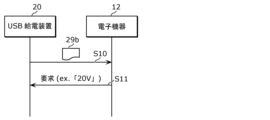
- FIG. 2 is a communication sequence diagram showing negotiation between the USB power supply device 20 and the electronic device 12 according to the embodiment.
- the control circuit 27 of the USB power supply device 20 connects the communication unit 28 and the communication terminal of the USB connector 25 to Then, the first table 29b stored in the storage unit 29 is transmitted to the electronic device 12 as information indicating one of the plurality of maximum output powers (S10).
- the electronic device 12 that has received the first table 29b sends the output voltage (e.g. , "20V") is transmitted (S11).
- the output voltage e.g. , "20V
- the control circuit 27 of the USB power supply device 20 Upon receiving the request for output voltage, the control circuit 27 of the USB power supply device 20 issues an instruction to the power supply circuit 22 to output the requested output voltage (for example, "20V").
- the requested output voltage for example, "20V"
- DC power at the output voltage requested by the electronic device 12 for example, the output voltage is 20 V, the maximum output current is 3 A, and the maximum output power is 60 W
- the output voltage is 20 V
- the maximum output current is 3 A
- the maximum output power is 60 W
- Such negotiation is executed by the control circuit 27 every time the output control tables (first table 29b, second table 29c, third table 29d) employed by the control circuit 27 are switched.
- the items to be negotiated are not limited to only the output voltage, but may include maximum output current and maximum output power.
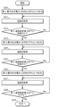
- FIG. 3 is a flowchart illustrating an operation example of output control by the USB power supply device 20 according to the embodiment.
- FIG. 4A is a diagram showing an operation curve for explaining the operation example shown in the flowchart of FIG. 3.
- FIG. 4B is a diagram showing an operation curve illustrating another operation example shown in the flowchart of FIG. 3.
- FIG. More specifically, the upper diagrams in FIGS. 4A and 4B show the time course of the maximum output power of the DC power supplied from the USB power supply device 20, and the lower diagrams in FIGS. 4A and 4B show the temperature detection of the USB power supply device 20. 3 shows a change in temperature detected by the circuit 26 over time.
- the control circuit 27 of the USB power supply device 20 performs control in the initial state.
- the power supply circuit 22 is controlled so that the output voltage of the power supply circuit 22 is the value determined by negotiation, and the maximum output power is the first maximum output power in the correspondence table 29a (S20 in FIG. 3).
- control of the output voltage is realized by the power supply circuit 22 receiving an output voltage instruction from the control circuit 27 and performing constant voltage control so as to output the instructed output voltage. Further, the maximum output power is controlled by the control circuit 27 monitoring the current detected by the output detection circuit 24 and feeding it back to the power supply circuit 22 so that the current does not exceed the current corresponding to the maximum output power. Realized.
- the power supply circuit 22 has the voltage determined by negotiation and the maximum output power becomes the first maximum output power (here, 60 W (100%)). DC power is supplied to the electronic device 12 in this state. As a result, as shown in the lower diagram of period 1 in FIG. 4A, during period 1, the temperature detected by the temperature detection circuit 26 increases.
- the control circuit 27 acquires the temperature detected by the temperature detection circuit 26 (S21 in FIG. 3), and the acquired temperature is the first temperature setting value (corresponding to the first maximum output power in the correspondence table 29a) ( Here, it is determined whether the temperature exceeds 80° C. (S22 in FIG. 3). If the temperature has not been exceeded (No in S22 of FIG. 3), the acquisition of the temperature (S21 of FIG. 3) and the determination (S22 of FIG. 3) are repeated until it is determined that the temperature has been exceeded.
- the control circuit 27 maintains the output voltage in order to suppress the temperature rise. In other words, the power supply circuit 22 is controlled so that the maximum output power becomes the second maximum output power in the correspondence table 29a (S23 in FIG. 3).
- the power supply circuit 22 supplies DC power to the electronic device 12 at the second maximum output power (here, 45 W (75%)).
- the maximum output power is suppressed in period 2, and the rate of increase in temperature detected by the temperature detection circuit 26 is suppressed compared to period 1.
- the control circuit 27 acquires the temperature detected by the temperature detection circuit 26 (S24 in FIG. 3), and the acquired temperature is the second temperature setting value (corresponding to the second maximum output power in the correspondence table 29a) ( Here, it is determined whether the temperature exceeds 85° C. (S25 in FIG. 3). If the temperature has not been exceeded (No in S25 in FIG. 3), the acquisition of the temperature (S24 in FIG. 3) and the determination (S25 in FIG. 3) are repeated until it is determined that the temperature has been exceeded.
- the control circuit 27 maintains the output voltage in order to further suppress the temperature rise. In this state, the maximum output power is switched to further decrease, that is, the power supply circuit 22 is controlled so that the maximum output power becomes the third maximum output power in the correspondence table 29a (S26 in FIG. 3).
- the power supply circuit 22 supplies DC power to the electronic device 12 at the third maximum output power (here, 30 W (50%)).
- the maximum output power is further suppressed in period 3, so that in this example, the temperature detected by the temperature detection circuit 26 has increased from the previous increase. Turns to a downward trend.
- the control circuit 27 acquires the temperature detected by the temperature detection circuit 26 (S27 in FIG. 3), and the acquired temperature corresponds to the third temperature setting value (corresponding to the third maximum output power in the correspondence table 29a). Here, it is determined whether the temperature has reached 65° C. or lower (S28 in FIG. 3). If the temperature is not equal to or lower than the third temperature setting value (No in S28 of FIG. 3), the process from temperature acquisition (S27 of FIG. 3) onward is repeated.
- the control circuit 27 determines that the temperature increase has been resolved, and outputs Switch to increase maximum output power while maintaining voltage. Specifically, the control circuit 27 performs control in the initial state (S20 in FIG. 3), that is, controls the power supply circuit 22 so that the maximum output power becomes the first maximum output power in the correspondence table 29a (FIG. 3). S29, S20).
- the power supply circuit 22 supplies DC power to the electronic device 12 at the first maximum output power (here, 60 W (100%)).
- the maximum output power is switched to increase, so the temperature detected by the temperature detection circuit 26 increases from the previous decrease.
- the temperature detection circuit 26 continues to detect However, unlike this operation example, if the temperature detected by the temperature detection circuit 26 starts to decrease, the operating curve of the USB power supply device 20 will become as shown in FIG. 4B. .
- the USB power supply device 20 when the USB power supply device 20 according to the present embodiment is supplying power at the first maximum output power, when the temperature detected by the temperature detection circuit 26 rises, the USB power supply device 20 suddenly outputs the minimum output power. Rather than switching to the third maximum output power, the second maximum output power is first switched to an intermediate second maximum output power that is smaller than the first maximum output power but larger than the smallest third maximum output power. After that, if the temperature continues to rise, the power is switched to the minimum third maximum output power (Fig. 4A), but if the temperature rise is eliminated, the intermediate second maximum output power is maintained. ( Figure 4B).
- step S28 in FIG. 3 After the power supply circuit 22 is controlled so that the maximum output power becomes the third maximum output power (here, 30 W (50%)) (S26 in FIG. 3), temperature detection is performed. It is determined whether the temperature detected by the circuit 26 has become equal to or lower than the third temperature set value (here, 65° C.) (27 to S28 in FIG. 3), but the determination of the third temperature set value ( In addition to step S28 in FIG. Processing may be performed to control the power to be lower than the maximum output power or to stop the output. This is because such a case may occur when multiple USB power supply devices 20 are connected.
- the third temperature set value here, 65° C.
- the maximum output power is changed by comparing the temperature detected by the temperature detection circuit 26 and the threshold temperature (that is, the first to third temperature setting values).
- the USB power supply device 20 has a control mode in which the maximum output power is changed using elapsed time.
- FIG. 5 is a flowchart showing another operation example of output control by the USB power supply device 20 according to the embodiment.
- a control step S30 to S31, S32 to S33 in FIG. 5 for changing the maximum output power using elapsed time is added to the flowchart shown in FIG. 3.
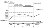
- FIG. 6A is a diagram showing an operation curve for explaining the operation example shown in the flowchart of FIG. 5.
- FIG. 6B is a diagram showing an operation curve illustrating another operation example shown in the flowchart of FIG. 5.
- FIG. More specifically, the upper diagrams in FIGS. 6A and 6B show the time course of the maximum output power of the DC power supplied from the USB power supply device 20, and the lower diagrams in FIGS. 6A and 6B show the temperature detection of the USB power supply device 20. 3 shows a change in temperature detected by the circuit 26 over time.
- the control circuit 27 of the USB power supply device 20 After switching the maximum output power from the first maximum output power to the second maximum output power (S23 in FIG. 5, time t1 in FIG. 6A), the control circuit 27 of the USB power supply device 20 starts a built-in timer (S23 in FIG. 5, time t1 in FIG. 6A). 5 S30), it is determined whether a preset first predetermined time ⁇ t1 (for example, 30 seconds) has elapsed (S31 in FIG. 5).
- a preset first predetermined time ⁇ t1 for example, 30 seconds
- the control circuit 27 performs the same process as the operation example in FIG. 3 (temperature acquisition (S24 of FIG. 5). ), the determination is made (S25 in FIG. 5)), but if it is determined that the first predetermined time ⁇ t1 has elapsed (Yes in S31 in FIG. 5, time t2 in FIG. 6A), it is determined that the temperature rise has been resolved. Then, switch to increase the maximum output power while maintaining the output voltage. Specifically, the control circuit 27 controls the power supply circuit 22 in the initial state (S20 in FIG. 5), that is, controls the power supply circuit 22 so that the maximum output power becomes the first maximum output power in the correspondence table 29a (S20 in FIG. 5). S20).
- the power supply circuit 22 outputs the first maximum output power (here, 60 W (100%)), DC power is supplied to the electronic device 12.
- the maximum output power is switched to increase in period 3, so in this example, the temperature detected by the temperature detection circuit 26 is turns from a decline to an increase.
- the control circuit 27 starts the built-in timer. (S32 in FIG. 5), and it is determined whether a second predetermined time ⁇ t2 (for example, 1 minute) has elapsed (S33 in FIG. 5).
- the control circuit 27 performs the same process as the operation example in FIG. ), the determination is made (S28 in FIG. 5)), but if it is determined that the second predetermined time ⁇ t2 has elapsed (Yes in S33 in FIG. 5, time t3 in FIG. 6B), it is determined that the temperature rise has been resolved. Then, the maximum output power is switched to increase while maintaining the output voltage, that is, control in the initial state (S20 in FIG. 5), that is, the maximum output power becomes the first maximum output power in the correspondence table 29a.
- the power supply circuit 22 is controlled as follows (S20 in FIG. 5).
- the power supply circuit 22 outputs the first maximum output power (here, 60 W (100%)), DC power is supplied to the electronic device 12.
- the maximum output power is switched to increase, so in this example, the temperature detected by the temperature detection circuit 26 is turns from a decline to an increase.
- the maximum output power is A comparison is also made between the elapsed time after switching the power and a predetermined time (S31, S33 in FIG. 5). If the elapsed time after switching the maximum output power exceeds a predetermined time, even if the temperature detected by the temperature detection circuit 26 has not reached the temperature setting value, the maximum output power of the power supply circuit 22 is changed. The first maximum output power is switched to the first maximum output power, and the maximum output power is increased.
- FIG. 7 is a flowchart showing control of the cutoff unit 23 by the USB power supply device 20 according to the embodiment.
- the control circuit 27 performs the following processing in parallel with the output control shown in FIGS. 3 and 5.
- the control circuit 27 uses the direct current detected by the output detection circuit 24 (that is, the output current) or the direct current power (that is, the product of the direct current and the output voltage instructed to the power supply circuit 22).
- output power S40
- control causes the cutoff unit 23 to cut off the output of the power supply circuit 22.
- S42 If at least one of the acquired DC power and DC current does not exceed the predetermined value (No in S41), the process returns to step S40 and the process is repeated.
- control circuit 27 cuts off the output of the power supply circuit 22 by the cutoff section 23, but instead of this, or in addition to this, as shown in FIG.
- the supply of DC power from the conversion circuit 21 to the power supply circuit 22a may be interrupted.
- FIG. 8 is a block diagram showing the configuration of a USB power supply device 20a according to a modification of the embodiment.
- a cutoff section 23a connected between the conversion circuit 21 and the power supply circuit 22a is provided here.
- the power supply circuit 22a controls the direct current detected by the output detection circuit 24 (that is, the output current), and the direct current detected by the output detection circuit 24.
- the DC power that is, the output power
- the interrupter 23a is activated.
- control is performed to cut off the supply of DC power from the conversion circuit 21 to the power supply circuit 22a.
- the interrupting section 23a in addition to the interrupting section 23, it is possible to prevent an overcurrent in which at least one of the actual output current and output power exceeds the maximum output current or maximum output power as a control target, or When an overpower supply state occurs, the supply of DC power to the electronic device 12 is reliably cut off, and damage to the USB power supply device 20a and the electronic device 12 is suppressed.
- the USB power supply device 20a according to this modification has a double cutoff structure including the cutoff part 23 and the cutoff part 23a, it may have only the cutoff part 23a. Even with such a configuration, at least the same safety as the USB power supply device 20 according to the embodiment including the cutoff section 23 is ensured.
- the USB power supply device 20 includes (Technology 1) a USB connector 25 having a power terminal, a circuit board 30 that supports the USB connector 25, and a conversion circuit mounted on the circuit board 30. 21, a power supply circuit 22, a temperature detection circuit 26, and a control circuit 27, the conversion circuit 21 converts AC power to DC power, and the power supply circuit 22 adjusts the DC power converted by the conversion circuit 21.
- the temperature detection circuit 26 detects the temperature of at least one part of the USB power supply device 20, and the control circuit 27 outputs the temperature detected by the temperature detection circuit 26 and a plurality of predetermined maximum outputs to the power supply terminal.
- the maximum output power of the power supply circuit 22 is controlled based on a plurality of temperature setting values determined corresponding to each power.
- the maximum output power of the power supply circuit 22 is determined based on the temperature detected by the temperature detection circuit 26 and a plurality of temperature setting values determined corresponding to each of a plurality of predetermined maximum output powers.
- this technology ensures safe temperature rise suppression and allows the user to use fine-grained output control. Convenience can also be ensured.
- the control circuit 27 controls the temperature when controlling the power supply circuit 22 so that the maximum output power of the power supply circuit 22 becomes the first maximum output power of the plurality of maximum output powers.
- the maximum output power of the power supply circuit 22 becomes one of the plurality of maximum output powers.
- the USB power supply device 20 according to technique 1, which controls the power supply circuit 22 to have a second maximum output power different from the first maximum output power. Thereby, the maximum output power is switched based on a comparison between the temperature detected by the temperature detection circuit 26 and the corresponding temperature setting value.
- the plurality of maximum output powers include at least three maximum output powers
- the plurality of temperature set values include at least three temperature set values corresponding to each of the at least three maximum output powers.
- the included USB power supply device 20 according to technology 1 or technology 2.
- the plurality of maximum output powers include, in descending order of magnitude, a first maximum output power, a second maximum output power, and a third maximum output power
- the plurality of temperature setting values include: A first temperature set value, a second temperature set value, and a third temperature set value corresponding to each of the first maximum output power, the second maximum output power, and the third maximum output power are included, and the second temperature set value
- the USB power supply device 20 according to any one of techniques 1 to 3, wherein >first temperature setting value>third temperature setting value holds.
- the USB power supply device 20 further includes a storage unit 29 that stores a correspondence table 29a and the like in which a plurality of maximum output powers and a plurality of temperature setting values are associated with each other.
- the described USB power supply device 20 This makes it possible to change the content of output control by rewriting the correspondence table 29a stored in the storage unit 29.
- the control circuit 27 controls the power supply circuit 22 so that the maximum output power of the power supply circuit 22 becomes the third maximum output power of the plurality of maximum output powers
- the control circuit 27 controls the temperature detection circuit
- the maximum output power of the power supply circuit 22 becomes one of the plurality of maximum output powers.
- the USB power supply device 20 according to any one of techniques 1 to 5, which controls the power supply circuit 22 so that the first maximum output power is larger than the third maximum output power of the USB power supply device 20.
- the control circuit 27 further controls the power supply circuit 22 so that the maximum output power of the power supply circuit 22 becomes the third maximum output power of the plurality of maximum output powers, and then a predetermined period of time has elapsed.
- any of the techniques 1 to 7 controls the power supply circuit 22 so that the maximum output power of the power supply circuit 22 becomes the first maximum output power that is larger than the third maximum output power among the plurality of maximum output powers.
- a USB power supply device 20 according to the invention. This prevents the power supply from being continued at the suppressed maximum output power, and allows the supply at a large output power to be resumed as soon as possible.
- the control circuit 27 further controls the temperature detected by the temperature detection circuit 26 when controlling the power supply circuit 22 so that the maximum output power of the power supply circuit 22 becomes the third maximum output power.
- power supply circuit 22 so that the maximum output power of power supply circuit 22 becomes the first maximum output power when The USB power supply device 20 according to technique 8, which controls the.
- the USB power supply device 20 further includes a communication unit 28 that communicates with the electronic device 12 to which DC power is supplied via the USB connector 25, and the control circuit 27 controls the electronic device 12 to receive DC power.
- the USB power supply device 20 according to any one of techniques 1 to 9, which transmits information indicating one of the plurality of maximum output powers to the electronic device 12 via the communication unit 28 before being supplied. This enables negotiation between the USB power supply device 20 and the electronic device 12, and enables the USB power supply device 20 to supply DC power that meets the requirements of the electronic device 12, making it compatible with electronic devices 12 of various specifications. A highly functional USB power supply device 20 is realized.
- the USB power supply device 20 further includes an output detection circuit 24 that detects at least one of DC power and DC current output from the power supply circuit 22, and a cutoff section 23 that cuts off the output of the power supply circuit 22.
- at least one of the power supply circuit 22 and the control circuit 27 controls the output of the power supply circuit 22 to the cutoff unit 23 when at least one of the DC power and the DC current detected by the output detection circuit 24 exceeds a predetermined value.
- the USB power supply device 20 according to any one of Techniques 1 to 10, which performs control to cut off the power.
- the electronic device 12 when an overcurrent or overpower supply state occurs in which at least one of the actual output current and output power exceeds the maximum output current or maximum output power as a control target, the electronic device 12 The supply of DC power to the USB power supply device 20 and the electronic device 12 can be prevented from being damaged.
- the USB power supply device 20a further includes an output detection circuit 24 that detects at least one of the DC power and the DC current output by the power supply circuit 22, and a At least one of the power supply circuit 22 and the control circuit 27 includes a cutoff section 23a that cuts off the supply of DC power, and when at least one of the DC power and the DC current detected by the output detection circuit 24 exceeds a predetermined value,
- the USB power supply device 20 according to any one of techniques 1 to 11, which controls the cutoff section 23a to cut off the supply of DC power from the conversion circuit 21 to the power supply circuit 22.
- the electronic device 12 when an overcurrent or overpower supply state occurs in which at least one of the actual output current and output power exceeds the maximum output current or maximum output power as a control target, the electronic device 12 The supply of DC power to the USB power supply device 20a and the electronic device 12 can be prevented from being damaged.
- the method for controlling the USB power supply device 20 includes (Technology 13) the steps of acquiring the temperature detected by the temperature detection circuit 26 (S21, S24, S27, etc. in FIG. 3), and A step of controlling the maximum output power of the power supply circuit 22 based on a plurality of temperature setting values determined corresponding to each of a plurality of predetermined maximum output powers (S22 to S23, S25 in FIG. 3). ⁇ S26, S28 ⁇ S29).
- the maximum output power of the power supply circuit 22 is determined based on the temperature detected by the temperature detection circuit 26 and a plurality of temperature setting values determined corresponding to each of a plurality of predetermined maximum output powers.
- this technology ensures safe temperature rise suppression and allows the user to use fine-grained output control. Convenience can also be ensured.
- the method for controlling the USB power supply device 20 may be realized as a program that causes a computer to execute the steps included in the method for controlling the USB power supply devices 20 and 20a (Technique 14).
- the program may be realized as a non-transitory recording medium such as a computer-readable DVD on which the program is recorded.
- USB power feeding device and its control method according to the present disclosure have been described above based on the embodiments and modifications, the present disclosure is not limited to these embodiments and modifications. Unless departing from the gist of the present disclosure, various modifications that can be thought of by those skilled in the art are made to this embodiment or the modified example, or other forms constructed by combining some of the components of the embodiment and the modified example. are also within the scope of this disclosure.
- three maximum output powers and three temperature setting values corresponding to them are registered in the correspondence table 29a, but the registered maximum output power and temperature setting values are divided into three sets.
- the number is not limited to two, or may be four or more. Even if there are two sets of maximum output power and temperature setting values registered in the correspondence table 29a, finer output control is performed based on temperature and elapsed time than in the conventional technology, and safe temperature rise control and user convenience are achieved. It is possible to achieve both.
- the common correspondence table 29a is used to control the output over time after switching the maximum output power and the temperature detected by the temperature detection circuit 26.
- both output controls by comparison with temperature setpoints were performed in parallel, these two output controls may be performed using different correspondence tables (ie, different maximum output powers).
- a cutoff part 23a connected between the conversion circuit 21 and the power supply circuit 22 is provided in place of the cutoff part 23 in FIG.
- a cutoff section 23a connected between the conversion circuit 21 and the power supply circuit 22 may be provided.
- the output detection circuit 24 similar to that in the embodiment is used to control the cut-off section 23a, but instead of or in addition to this, the output detection circuit 24 is connected between the conversion circuit 21 and the power supply circuit 22.
- a connected output detection circuit for example composed of a shunt resistor, may also be used.
- the cutoff section 23a is controlled by the power supply circuit 22, it may be controlled by the control circuit 27 instead of or in addition to this.
- the maximum output current and the maximum output power are registered in the first to third tables 29b to 29d, but it is not necessary that both are registered, and only one of them is registered. You can leave it there.
- a user interface may be provided to rewrite the correspondence table 29a and the first to third tables 29b to 29d stored in the storage unit 29 according to instructions from the user.
- the user interface can be realized, for example, by the control circuit 27 having a conversation with the user's terminal device via the communication unit 28.
- the USB power supply device is a USB power supply device that can achieve both safe temperature rise control and user convenience, and is, for example, in the form of a portable power adapter that is used by being plugged into a commercial power outlet. It can be used as a USB power supply device or a USB power supply device in the form of an embedded wiring device that is embedded and fixed in a wall or the like.
Landscapes
- Engineering & Computer Science (AREA)
- Theoretical Computer Science (AREA)
- Physics & Mathematics (AREA)
- General Engineering & Computer Science (AREA)
- General Physics & Mathematics (AREA)
- Human Computer Interaction (AREA)
- Power Engineering (AREA)
- Direct Current Feeding And Distribution (AREA)
- Control Of Voltage And Current In General (AREA)
Priority Applications (1)
| Application Number | Priority Date | Filing Date | Title |
|---|---|---|---|
| JP2024539097A JPWO2024029417A1 (https=) | 2022-08-05 | 2023-07-26 |
Applications Claiming Priority (2)
| Application Number | Priority Date | Filing Date | Title |
|---|---|---|---|
| JP2022-125148 | 2022-08-05 | ||
| JP2022125148 | 2022-08-05 |
Publications (1)
| Publication Number | Publication Date |
|---|---|
| WO2024029417A1 true WO2024029417A1 (ja) | 2024-02-08 |
Family
ID=89849018
Family Applications (1)
| Application Number | Title | Priority Date | Filing Date |
|---|---|---|---|
| PCT/JP2023/027331 Ceased WO2024029417A1 (ja) | 2022-08-05 | 2023-07-26 | Usb給電装置及びその制御方法 |
Country Status (3)
| Country | Link |
|---|---|
| JP (1) | JPWO2024029417A1 (https=) |
| TW (1) | TWI856755B (https=) |
| WO (1) | WO2024029417A1 (https=) |
Citations (4)
| Publication number | Priority date | Publication date | Assignee | Title |
|---|---|---|---|---|
| US20180232021A1 (en) * | 2017-02-16 | 2018-08-16 | Astronics Advanced Electronic Systems Corp. | Control of Temperature in a USB Type C Source through Re-Negotiation of Power Delivery Object |
| US20200328686A1 (en) * | 2019-04-12 | 2020-10-15 | Stmicroelectronics (Grenoble 2) Sas | Universal serial bus type-c connection interface |
| US20210208648A1 (en) * | 2020-01-08 | 2021-07-08 | Cypress Semiconductor Corporation | Dynamic power throttling based on system conditions in usb type-c power delivery (usb-c/pd) ecosystem |
| US20220269327A1 (en) * | 2021-02-23 | 2022-08-25 | Dell Products L.P. | External power supply and method to enhance the output power delivered by an external power supply |
Family Cites Families (11)
| Publication number | Priority date | Publication date | Assignee | Title |
|---|---|---|---|---|
| DE10203051A1 (de) * | 2002-01-26 | 2003-08-14 | Bosch Gmbh Robert | Verfahren und Vorrichtung zur temperaturabhängigen Steuerung von Leistung eines Elektrogerätes |
| JP2006271136A (ja) * | 2005-03-24 | 2006-10-05 | Denso Corp | Dc−dcコンバータ装置 |
| KR101885857B1 (ko) * | 2012-01-04 | 2018-08-06 | 삼성전자주식회사 | 온도 관리 회로, 이를 포함하는 시스템 온 칩 및 온도 관리 방법 |
| TWI486780B (zh) * | 2013-08-13 | 2015-06-01 | Phison Electronics Corp | 連接介面單元與記憶體儲存裝置 |
| US10474208B2 (en) * | 2016-03-31 | 2019-11-12 | Intel Corporation | Systems, methods and devices for using thermal margin of a core in a processor |
| US10528099B2 (en) * | 2016-10-10 | 2020-01-07 | Micron Technology, Inc. | Configuration update for a memory device based on a temperature of the memory device |
| CN206523836U (zh) * | 2016-12-16 | 2017-09-26 | 算丰科技(北京)有限公司 | 串联供电芯片和系统 |
| WO2018168116A1 (ja) * | 2017-03-15 | 2018-09-20 | 株式会社日立製作所 | 電力変換装置の診断回路、電力変換装置の診断システム |
| US10664365B2 (en) * | 2017-08-21 | 2020-05-26 | Google Llc | System and method for monitoring and controlling a back-up power supply using temperature controlled batteries |
| WO2020084756A1 (ja) * | 2018-10-26 | 2020-04-30 | 日本たばこ産業株式会社 | 電子装置並びに電子装置を動作させる方法及びプログラム |
| JP2021040364A (ja) * | 2019-08-30 | 2021-03-11 | 沖電気工業株式会社 | 電源回路 |
-
2023
- 2023-07-26 JP JP2024539097A patent/JPWO2024029417A1/ja active Pending
- 2023-07-26 WO PCT/JP2023/027331 patent/WO2024029417A1/ja not_active Ceased
- 2023-07-27 TW TW112128085A patent/TWI856755B/zh active
Patent Citations (4)
| Publication number | Priority date | Publication date | Assignee | Title |
|---|---|---|---|---|
| US20180232021A1 (en) * | 2017-02-16 | 2018-08-16 | Astronics Advanced Electronic Systems Corp. | Control of Temperature in a USB Type C Source through Re-Negotiation of Power Delivery Object |
| US20200328686A1 (en) * | 2019-04-12 | 2020-10-15 | Stmicroelectronics (Grenoble 2) Sas | Universal serial bus type-c connection interface |
| US20210208648A1 (en) * | 2020-01-08 | 2021-07-08 | Cypress Semiconductor Corporation | Dynamic power throttling based on system conditions in usb type-c power delivery (usb-c/pd) ecosystem |
| US20220269327A1 (en) * | 2021-02-23 | 2022-08-25 | Dell Products L.P. | External power supply and method to enhance the output power delivered by an external power supply |
Also Published As
| Publication number | Publication date |
|---|---|
| TWI856755B (zh) | 2024-09-21 |
| TW202408137A (zh) | 2024-02-16 |
| JPWO2024029417A1 (https=) | 2024-02-08 |
Similar Documents
| Publication | Publication Date | Title |
|---|---|---|
| US6127882A (en) | Current monitors with independently adjustable dual level current thresholds | |
| TWI551016B (zh) | Power supply and power supply method | |
| US9252669B2 (en) | AC/DC converter, and AC power adapter and electronic apparatus using the same | |
| TWI483508B (zh) | 用於控制電力分配的方法及裝置 | |
| TWI620404B (zh) | 一種可應用於外接式硬碟之電源轉換電路 | |
| TWI523359B (zh) | 過電壓保護裝置及其操作方法 | |
| JP6063502B2 (ja) | 過負荷保護および省電力機構を備えた電力伝送装置 | |
| US20110055614A1 (en) | Power-supply expansion system and method thereof | |
| CN101312303A (zh) | 电源切换装置 | |
| CN101151787A (zh) | 开关式电源 | |
| JP2016208614A (ja) | 過電流保護付き電源装置 | |
| CN103795277B (zh) | 具有输出保护功能的电源供应器及其控制方法 | |
| WO2024029417A1 (ja) | Usb給電装置及びその制御方法 | |
| CN103427617A (zh) | 电源电路 | |
| JPH11308857A (ja) | スイッチング電源装置 | |
| CN218897162U (zh) | 一种电源切换电路及电子设备 | |
| TWI662778B (zh) | 可調整功耗限制的電源供應器及調整功耗限制的方法 | |
| CN106505406B (zh) | 激光器工作状态的控制方法及光模块 | |
| CN108075631B (zh) | 家用电器及其泄压装置 | |
| CN106356967B (zh) | 一种适配器以及配置有所述适配器的电子设备 | |
| JP5277706B2 (ja) | スイッチング電源装置 | |
| KR101964628B1 (ko) | 별도의 배선추가 없이 교류전원 벽스위치를 이용한 led 조명제어장치 및 그 제어 방법 | |
| CN206422950U (zh) | 一种触摸调光开关 | |
| KR101367969B1 (ko) | 콘센트 장치 및 그의 제어방법 | |
| CN104953649A (zh) | 一种供电电路及电子设备 |
Legal Events
| Date | Code | Title | Description |
|---|---|---|---|
| 121 | Ep: the epo has been informed by wipo that ep was designated in this application |
Ref document number: 23849972 Country of ref document: EP Kind code of ref document: A1 |
|
| WWE | Wipo information: entry into national phase |
Ref document number: 2024539097 Country of ref document: JP |
|
| WWE | Wipo information: entry into national phase |
Ref document number: 202517004036 Country of ref document: IN |
|
| WWE | Wipo information: entry into national phase |
Ref document number: 2501000423 Country of ref document: TH |
|
| WWP | Wipo information: published in national office |
Ref document number: 202517004036 Country of ref document: IN |
|
| NENP | Non-entry into the national phase |
Ref country code: DE |
|
| 122 | Ep: pct application non-entry in european phase |
Ref document number: 23849972 Country of ref document: EP Kind code of ref document: A1 |