WO2024029409A1 - 反射型マスクブランク及び反射型マスク - Google Patents
反射型マスクブランク及び反射型マスク Download PDFInfo
- Publication number
- WO2024029409A1 WO2024029409A1 PCT/JP2023/027271 JP2023027271W WO2024029409A1 WO 2024029409 A1 WO2024029409 A1 WO 2024029409A1 JP 2023027271 W JP2023027271 W JP 2023027271W WO 2024029409 A1 WO2024029409 A1 WO 2024029409A1
- Authority
- WO
- WIPO (PCT)
- Prior art keywords
- absorption layer
- reflective mask
- pattern
- light
- film
- Prior art date
- Legal status (The legal status is an assumption and is not a legal conclusion. Google has not performed a legal analysis and makes no representation as to the accuracy of the status listed.)
- Ceased
Links
Images


Classifications
-
- G—PHYSICS
- G03—PHOTOGRAPHY; CINEMATOGRAPHY; ANALOGOUS TECHNIQUES USING WAVES OTHER THAN OPTICAL WAVES; ELECTROGRAPHY; HOLOGRAPHY
- G03F—PHOTOMECHANICAL PRODUCTION OF TEXTURED OR PATTERNED SURFACES, e.g. FOR PRINTING, FOR PROCESSING OF SEMICONDUCTOR DEVICES; MATERIALS THEREFOR; ORIGINALS THEREFOR; APPARATUS SPECIALLY ADAPTED THEREFOR
- G03F1/00—Originals for photomechanical production of textured or patterned surfaces, e.g., masks, photo-masks, reticles; Mask blanks or pellicles therefor; Containers specially adapted therefor; Preparation thereof
- G03F1/22—Masks or mask blanks for imaging by radiation of 100nm or shorter wavelength, e.g. X-ray masks, extreme ultraviolet [EUV] masks; Preparation thereof
- G03F1/24—Reflection masks; Preparation thereof
-
- G—PHYSICS
- G03—PHOTOGRAPHY; CINEMATOGRAPHY; ANALOGOUS TECHNIQUES USING WAVES OTHER THAN OPTICAL WAVES; ELECTROGRAPHY; HOLOGRAPHY
- G03F—PHOTOMECHANICAL PRODUCTION OF TEXTURED OR PATTERNED SURFACES, e.g. FOR PRINTING, FOR PROCESSING OF SEMICONDUCTOR DEVICES; MATERIALS THEREFOR; ORIGINALS THEREFOR; APPARATUS SPECIALLY ADAPTED THEREFOR
- G03F1/00—Originals for photomechanical production of textured or patterned surfaces, e.g., masks, photo-masks, reticles; Mask blanks or pellicles therefor; Containers specially adapted therefor; Preparation thereof
- G03F1/26—Phase shift masks [PSM]; PSM blanks; Preparation thereof
- G03F1/32—Attenuating PSM [att-PSM], e.g. halftone PSM or PSM having semi-transparent phase shift portion; Preparation thereof
-
- G—PHYSICS
- G03—PHOTOGRAPHY; CINEMATOGRAPHY; ANALOGOUS TECHNIQUES USING WAVES OTHER THAN OPTICAL WAVES; ELECTROGRAPHY; HOLOGRAPHY
- G03F—PHOTOMECHANICAL PRODUCTION OF TEXTURED OR PATTERNED SURFACES, e.g. FOR PRINTING, FOR PROCESSING OF SEMICONDUCTOR DEVICES; MATERIALS THEREFOR; ORIGINALS THEREFOR; APPARATUS SPECIALLY ADAPTED THEREFOR
- G03F1/00—Originals for photomechanical production of textured or patterned surfaces, e.g., masks, photo-masks, reticles; Mask blanks or pellicles therefor; Containers specially adapted therefor; Preparation thereof
- G03F1/54—Absorbers, e.g. of opaque materials
- G03F1/58—Absorbers, e.g. of opaque materials having two or more different absorber layers, e.g. stacked multilayer absorbers
Definitions
- the present invention relates to a reflective mask blank used in extreme ultraviolet (EUV) lithography in semiconductor manufacturing, etc., and a reflective mask using the same.
- EUV extreme ultraviolet
- a reflective mask used in EUV lithography has a mask pattern made of an absorption layer that absorbs EUV light on a multilayer reflective film that reflects EUV light with a short wavelength of about 13.5 nm.
- a reflective mask has a thick absorption layer, dimensional errors in the transferred pattern are likely to occur due to so-called shadowing, in which obliquely incident (usually at an incident angle of 6 degrees) EUV light and its reflected light are blocked.
- phase shift mask technology improves the resolution of the edge portion of the transferred pattern by absorbing EUV light and using an absorption layer formed so that the reflected light has a different phase from the reflected light from the multilayer reflective film. Development is also underway.
- a material or shape having a different refractive index or transmittance than that of the transmission part is added to the transmission part of the mask pattern, and the phase of the transmitted light in this part is changed, thereby increasing the resolution. It is intended to improve In the region where the phase is changed, the transmitted diffracted lights having a phase difference interfere with each other, and the light intensity decreases. As a result, the contrast of the transferred pattern is improved, and as a result, the depth of focus during transfer is expanded and the transfer accuracy is improved.
- a halftone mask which is a type of transmission phase shift mask, has a thin film semi-transparent to exposure light formed in a portion that changes the phase of transmitted light.
- Halftone masks improve the resolution of pattern edges by attenuating the transmittance to about a few percent (usually about 2.5 to 15.0% of the light transmitted through the substrate) and changing the phase. By doing so, the transfer accuracy can be improved. Note that, in principle, the best phase difference is 180°, but it is known that an effect of improving resolution can be obtained if the phase difference is substantially about 175 to 185°.
- phase difference the phase difference in a conventional reflective mask is generally designed so that the phase difference is around 180° (almost inverted) (for example, see Patent Document 1).
- the absorption layer of a reflective mask has a phase difference of 180 mm based on the refractive index (hereinafter sometimes referred to as n) and extinction coefficient (hereinafter sometimes referred to as k) of the constituent materials.
- n refractive index
- k extinction coefficient
- the half pitch (1/2 of the total length of the line width and line interval; hereinafter abbreviated as HP) of the transferred pattern is usually used as a representative value for the dimension of a line pattern in microfabrication.
- HP is 16 nm or less
- LSI patterns are becoming more complex as the integration density increases, and they have a complex structure of orthogonal line patterns, and mask patterns must also accommodate such complex structures. There is.
- the present invention was made in view of these circumstances, and provides a reflective mask for EUV lithography that can form a transfer pattern with high dimensional accuracy in a fine line pattern, and a reflective mask blank used therein.
- the purpose is to provide.
- the present invention is based on the discovery that in fine line patterns in EUV lithography, it is possible to form a transferred pattern with high dimensional accuracy when the retardation due to the absorption layer is larger than before.
- a reflective mask blank for EUV lithography in which a multilayer reflective film that reflects EUV light and an absorption layer that absorbs EUV light are laminated in this order from the substrate side on a substrate, and the absorption layer has a refractive index of 0.930 or less for EUV light with a wavelength of 13.5 nm, and an extinction coefficient of 0.025 or more, and is A reflective mask blank, wherein the phase difference between the reflected light from the surface of the absorption layer and the reflected light from the surface of the absorption layer is 220 to 280°.
- the absorption layer is selected from iridium (Ir), rhenium (Re), osmium (Os), ruthenium (Ru), platinum (Pt), palladium (Pd), gold (Au) and silver (Ag).
- the absorption layer includes one or more metal elements selected from platinum (Pt), palladium (Pd), gold (Au), and silver (Ag), according to any one of [1] to [4].
- Reflective mask blank as described. [7] The reflective mask blank according to any one of [1] to [6], wherein the absorption layer has an extinction coefficient of 0.025 to 0.040 for EUV light with a wavelength of 13.5 nm. [8] The reflective mask blank according to any one of [1] to [7], wherein the absorption layer is formed by laminating two or more layers. [9] The reflective mask blank according to any one of [1] to [8], wherein the absorption layer has a total thickness of 60 nm or less. [10] The reflective mask blank according to any one of [1] to [9], wherein a protective film for protecting the multilayer reflective film is formed between the multilayer reflective film and the absorption layer.
- a reflective mask for EUV lithography in which a multilayer reflective film that reflects EUV light and an absorption layer that absorbs EUV light are laminated in this order from the substrate side on a substrate, the absorption layer comprising:
- the refractive index of EUV light with a wavelength of 13.5 nm is 0.930 or less and the extinction coefficient is 0.025 or more, and reflection from the surface of the multilayer reflective film with respect to incident light of EUV light with a wavelength of 13.5 nm.
- a reflective mask wherein a phase difference between light and reflected light from a surface of the absorption layer is 220 to 280°, and a mask pattern is formed on the absorption layer.
- N V ⁇ 2.80 (1) N H ⁇ 2.80 (2)
- the absorption layer is selected from iridium (Ir), rhenium (Re), osmium (Os), ruthenium (Ru), platinum (Pt), palladium (Pd), gold (Au) and silver (Ag).
- the reflective mask according to any one of [11] to [15], containing one or more metal elements.
- the absorption layer includes one or more metal elements selected from platinum (Pt), palladium (Pd), gold (Au), and silver (Ag), according to any one of [11] to [15].
- Reflective mask as described.
- a reflective mask for EUV lithography that can form a transfer pattern with high dimensional accuracy in a fine line pattern, and a reflective mask blank used therein.
- FIG. 3 is a schematic plan view of a line-and-space pattern transfer pattern, in which (a) shows a first line-shaped transfer pattern, and (b) shows a second line-shaped transfer pattern.
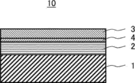
- 1 is a schematic cross-sectional view schematically showing a reflective mask according to an embodiment of the present invention.
- (b) is a diagram in which the phase difference calculated from the values of d, n, and k at this time is expressed by contour lines.
- (b) is a diagram in which the phase difference calculated from the values of d, n, and k at this time is expressed by contour lines.
- the terms "on a substrate, on a layer,” and on a film include not only the case where the material is in contact with the upper surface of the film, etc., but also the upper part that is not in contact with the upper surface of the film, etc.
- film B on film A may mean that film A and film B are in contact with each other, or that another film or the like may be interposed between film A and film B.
- above here does not necessarily mean a high position in the vertical direction, but indicates a relative positional relationship.
- the thickness of the formed film, etc. can be measured using a transmission electron microscope or an X-ray reflectance method.
- the preferable numerical range can be determined by arbitrarily combining each of the preferable lower limit and upper limit.
- FIG. 1 schematically shows a cross section of a reflective mask blank of this embodiment.
- a multilayer reflective film 2 that reflects EUV light and an absorption layer 3 that absorbs EUV light are laminated on a substrate 1 in this order from the substrate 1 side.
- a protective film 4 also called a cap layer
- an antireflection film (not shown) may be formed on the absorption layer 3 to facilitate pattern defect inspection after mask processing.
- the substrate 1 preferably has a low thermal expansion coefficient at 20°C, preferably 0 ⁇ 0.05 ⁇ 10 -7 /°C, more preferably 0 ⁇ It is 0.03 ⁇ 10 ⁇ 7 /°C. Further, it is preferable that the substrate 1 has excellent smoothness, high flatness, and excellent resistance (chemical resistance) to the cleaning liquid used in the manufacturing process of the reflective mask.
- the material of the substrate 1 include SiO 2 -TiO 2 glass, multi-component glass ceramics, etc., and crystallized glass in which ⁇ -quartz solid solution is precipitated, quartz glass, silicon, metal, etc. can also be used. .
- the substrate 1 is preferably smooth, and has a surface roughness (RMS) of preferably 0.15 nm or less, more preferably 0.10 nm or less. It is. From the same viewpoint, the flatness (TIR; Total Indicated Reading) is preferably 100 nm or less, more preferably 50 nm or less, and still more preferably 30 nm or less.
- RMS surface roughness
- TIR Total Indicated Reading
- the substrate 1 has high rigidity from the viewpoint of preventing deformation due to stress of a film or the like laminated thereon. Specifically, it is preferable that the Young's modulus is 65 GPa or more.
- the multilayer reflective film 2 preferably has a structure in which a plurality of layers containing elements having different refractive indexes as main components are periodically laminated.
- the multilayer reflective film 2 has a structure in which one period is a set of one high refractive index layer and one low refractive index layer, and about 40 to 60 periods are laminated.
- the high refractive index layer/low refractive index layer is generally a Mo/Si multilayer reflective film, but is not limited to this, and includes, for example, a Ru/Si multilayer reflective film, a Mo/Be multilayer reflective film, Mo compound/Si compound multilayer reflective film, Si/Mo/Ru multilayer reflective film, Si/Mo/Ru/Mo multilayer reflective film, MoRu/Si multilayer reflective film, Si/Ru/Mo multilayer reflective film, Si/Ru/Mo /Ru multilayer reflective film, etc. may also be mentioned.
- the multilayer reflective film 2 preferably has a reflectance of 60% or more, more preferably 65% or more of EUV light having a wavelength of around 13.5 nm and incident light at an incident angle of 6°.
- the thickness of each film constituting the multilayer reflective film 2 and the repetition period of lamination are appropriately set according to the film material, desired reflectance of EUV light, and the like.
- the multilayer reflective film 2 can be formed by forming each constituent film to a desired thickness using a known film forming method such as magnetron sputtering or ion beam sputtering.
- a known film forming method such as magnetron sputtering or ion beam sputtering.
- argon (Ar) gas gas pressure 1.3 ⁇ 10 ⁇ 2 to 2.7 ⁇ 10 ⁇ 2 Pa
- a Si film was first deposited to a thickness of 4.5 nm using a Si target, and then a Mo target was deposited.
- a Mo film is formed to a thickness of 2.3 nm using the following method. By repeating this as one cycle and stacking the Mo film/Si film for 30 to 60 cycles, a Mo/Si multilayer reflective film can be formed.
- a protective film 4 may be formed between the multilayer reflective film 2 and the absorption layer 3 to protect the multilayer reflective film 2 from dry etching when forming a mask pattern.
- the protective film 4 also has the role of preventing the multilayer reflective film 2 from being oxidized during EUV exposure and reducing the reflectance of EUV light.
- the etching gas a halogen-based gas, an oxygen-based gas, or a mixed gas thereof is usually used.
- halogen-based gas examples include a chlorine-based gas containing one or more selected from Cl 2 , SiCl 4 , CHCl 3 , CCl 4 and BCl 3 ; selected from CF 4 , CHF 3 , SF 6 , BF 3 and XeF 2
- fluorine-based gases examples include fluorine-based gases containing one or more of the following.
- the protective film 4 contains one or more elements selected from, for example, Ru, Rh, and Si.
- the protective film 4 may be a film made only of Rh, but it is also preferable that it contains one or more elements selected from Ru, Nb, Mo, Ta, Ir, Pd, Zr, Y, and Ti.
- one or more elements selected from Ru, Ta, Ir, Pd, and Y are preferred from the viewpoint of improving resistance to etching gas and sulfuric acid peroxide used for cleaning reflective masks.
- one or more elements selected from N, O, C, and B may be included.
- the protective film 4 may be a single layer or a multilayer film consisting of multiple layers.
- the lower layer of the protective film 4 may be formed so as to contact the uppermost surface of the multilayer reflective film 2
- the upper layer of the protective film 4 may be formed so as to contact the lowermost surface of the absorbing layer 3 .
- the protective film 4 may include a layer that does not contain Rh.
- the thickness of the protective film 4 means the total thickness of the multilayer film.
- the thickness of the protective film 4 may be within a range that can sufficiently fulfill the above-mentioned role without interfering with the reflective performance of the multilayer reflective film 2, and is preferably 1.0 to 10.0 nm, more preferably 2.0 nm to 10.0 nm. It is 0 to 3.5 nm. From the same viewpoint, the protective film 4 preferably has a root mean square roughness (RMS) of 0.3 nm or less, more preferably 0.1 nm or less, and is preferably smooth.
- RMS root mean square roughness
- the protective film 4 can be formed by forming a film to a desired thickness using a known film forming method such as DC sputtering, magnetron sputtering, or ion beam sputtering.
- a buffer layer (not shown) may be formed between the protective film 4 and the absorption layer 3 to protect the multilayer reflective film 2 during dry etching or defect correction.
- the material constituting the buffer layer is not particularly limited, and examples thereof include materials containing SiO 2 , Cr, Ta, etc. as main components.
- the absorption layer 3 has a refractive index of 0.930 or less for EUV light with a wavelength of 13.5 nm and an extinction coefficient of 0.025 or more, and is a multilayer reflective film 2 for the incident light of EUV light with a wavelength of 13.5 nm.
- the phase difference between the light reflected from the surface of the absorption layer 3 and the light reflected from the surface of the absorption layer 3 is 220 to 280°. Since the absorption layer 3 of the reflective mask blank of this embodiment has such characteristics, it is suitable for a reflective mask for EUV lithography that can transfer a fine line pattern with high dimensional accuracy.
- the refractive index of the absorption layer 3 for EUV light with a wavelength of 13.5 nm is 0.930 or less, preferably 0.925 or less, and more preferably 0.920 or less.
- the refractive index is preferably 0.850 or more.
- the extinction coefficient of EUV light with a wavelength of 13.5 nm of the absorption layer 3 is 0.025 or more, preferably 0.028 to 0.065, more preferably 0.030 to 0.050.
- the extinction coefficient is within the above range, a phase shift mask capable of transferring a fine line pattern with high dimensional accuracy can be obtained.
- the position of the reflected light from the surface of the multilayer reflective film 2 and the reflected light from the surface of the absorption layer 3 with respect to the incident light of EUV light with a wavelength of 13.5 nm must be adjusted.
- the phase difference is 220 to 280°, preferably 225 to 280°.
- EUV light with a wavelength of 13.5 nm that was directly incident is reflected by the multilayer reflective film 2 and passed through the opening of the mask pattern without passing through the absorption layer 3 again.
- reflected light from the surface of the absorption layer 3 means that incident light of EUV light with a wavelength of 13.5 nm is transmitted through the absorption layer 3 (and protective film 4) while being absorbed by the absorption layer 3, and the multilayer reflection film 2 This means the reflected light that is reflected by the absorption layer 3 and transmitted through the absorption layer 3 while being absorbed by the absorption layer 3 again.
- the absorption layer of a reflective mask for EUV lithography is desirably thin from the viewpoint of suppressing shadowing, and various constituent materials and structures have been studied. was considered the best.
- the phase difference uses a value calculated by optical multilayer film simulation, but can be roughly expressed by the following equation (4).
- ⁇ 4 ⁇ d/ ⁇ d/( ⁇ /n) ⁇ (4)
- ⁇ is the phase difference
- d is the thickness of the absorption layer 3
- ⁇ is the wavelength of the incident light
- n is the refractive index of the absorption layer 3.
- a preferred embodiment of the fine linear pattern formed on the absorption layer 3 of the reflective mask blank 10 is, for example, a mask pattern including a first linear pattern and a second linear pattern whose line directions are perpendicular to each other.
- the mask pattern formed on the absorption layer 3 of the reflective mask blank 10 is such that a first linear transfer pattern L1 as shown in FIG. 2(a) is formed on the transfer surface T by the first linear pattern.
- a second line-shaped transfer pattern L2 as shown in FIG. Preferably, it is for forming a pattern (LS pattern).
- the first linear transfer pattern L1 and the second linear transfer pattern L2 on the transfer surface T shown in FIGS. 2(a) and 2(b) both have the same line width and the same interval. , the width and the spacing, and the width and the spacing may be different. Further, it may include a portion where the lines intersect with each other.
- the reflective mask blank 10 is suitable when the transfer pattern formed by the first line pattern and the second line pattern includes, for example, a fine line pattern with HP of 18 nm or less; Preferably, HP is 16 nm or less. When the HP is within the above range, more excellent effects as a phase shift mask with high dimensional accuracy can be obtained.
- EUV lithography is a reduction projection exposure, and the reduction rate of the transferred pattern with respect to the mask pattern is usually 4 times.
- the mask pattern is an LS pattern with HP of 64 nm. Note that in the case of an LS pattern in which the line width and the line interval are different, the critical dimension (CD) of the line width at the resolution limit can be considered to correspond to the HP.
- the material constituting the absorption layer 3 is not particularly limited as long as it can form the phase shift mask as described above, but may be selected from Ir, Re, Os, Ru, Pt, Pd, Au, and Ag. It is preferable that one or more selected metal elements are included.
- the metal elements may be used alone or in combination of two or more. Further, the material may be a single metal element or an alloy, or may be a compound containing, for example, oxygen (O), nitrogen (N), carbon (C), boron (B), hydrogen (H), etc. .
- Examples of materials made of two types of metal elements include alloys such as PdCr, IrMo, OsRu, RuPt, RuIr, and OsRe.
- the composition ratio of each metal is not particularly limited as long as the refractive index and extinction coefficient of the absorption layer 3 satisfy the above numerical ranges.
- the constituent material of the absorption layer 3 is a PdCr alloy
- the ratio of the Cr content [at%] to the Pd content [at%] (Cr/Pd) is set to a desired value while suppressing crystallization of the absorption layer 3.
- the alloy may contain B, N, O, C, etc. for the purpose of controlling crystallinity.
- the ratio (Mo/Ir) of the Mo content [at%] to the Ir content [at%] is set to a desired value while suppressing crystallization of the absorption layer 3.
- it is preferably 0.01 to 4, more preferably 0.05 to 2, and even more preferably 0.1 to 1.
- the alloy may contain B, N, O, C, etc. for the purpose of controlling crystallinity.
- the ratio of the Ru content [at%] to the Os content [at%] (Ru/Os) is set to a desired value while suppressing crystallization of the absorption layer 3.
- it is preferably 0.01 to 4, more preferably 0.05 to 2, and even more preferably 0.1 to 1.
- the alloy may contain B, N, O, C, etc. for the purpose of controlling crystallinity.
- the ratio (Pt/Ru) of the Pt content [at%] to the Ru content [at%] is set to a desired value while suppressing crystallization of the absorption layer 3.
- the alloy may contain B, N, O, C, etc. for the purpose of controlling crystallinity.
- the ratio (Ir/Ru) of the Ir content [at%] to the Ru content [at%] is set to a desired value while suppressing crystallization of the absorption layer 3.
- it is preferably 0.01 to 20, more preferably 0.2 to 10, and even more preferably 0.4 to 4.
- the alloy may contain B, N, O, C, etc. for the purpose of controlling crystallinity.
- the ratio of the Re content [at%] to the Os content [at%] (Re/Os) is set to a desired value while suppressing crystallization of the absorption layer 3.
- it is preferably 0.01 to 20, more preferably 0.05 to 10, and even more preferably 0.1 to 5.
- the alloy may contain B, N, O, C, etc. for the purpose of controlling crystallinity.
- the absorbent layer 3 may have a multilayer structure in which two or more layers are laminated.
- a multilayer structure is preferable in that the entire absorbent layer 3 can be designed with each layer having a predetermined functional layer made of different materials.
- Functional layers include, for example, a buffer layer that is formed between the reflective layer and the absorbing layer as necessary to prevent damage to the reflective layer during patterning, and a buffer layer that improves the contrast during mask pattern inspection.
- a low reflection layer (a low reflection layer in the wavelength range of the mask pattern inspection light) formed as necessary on the top layer of the absorption layer 3 for the purpose of controlling the reflectance at EUV wavelengths. Examples include a phase control layer formed for the purpose of controlling the phase at EUV wavelength.
- layer combinations in the multilayer structure include Pt/Ru, Ir/Ru, Pt/Ta, Pt/Ta 2 O 5 , Ir/Cr, Ir/Ta 2 O 5 and the like.
- the constituent materials of these layers such as Pt, Ru, Ir, Ta, Ta2O5 , Cr, etc. may be alloys, nitrogen compounds, oxynitrides, etc., depending on the required properties such as optical properties, crystallinity, etching properties, and durability . It may be a substance, a boride, etc.
- the lamination order may be any order; for example, in the case of the above-mentioned two-layer structure, the order is preferably first layer/second layer.
- the refractive index and extinction coefficient are obtained as a weighted average value taking into account the thickness of each layer.
- the absorption layer 3 can be formed by forming each constituent film to a desired thickness using a known film forming method such as magnetron sputtering or ion beam sputtering.
- the total thickness of the absorption layer 3 is 60 nm or less, and it can be effective as a phase shift mask that can transfer fine line patterns with high dimensional accuracy while suppressing shadowing. .
- the total thickness of the absorption layer 3 is preferably thin from the viewpoint of etching efficiency during film formation of the absorption layer 3 and mask pattern formation, and is preferably 60 nm or less, more preferably 58 nm or less, and even more preferably 45 nm or less. It is. Further, the total thickness of the absorption layer 3 is preferably 20 nm or more from the viewpoint of the absorption effect of EUV light.
- An antireflection film may be laminated on the absorption layer 3 to prevent reflection when DUV light (deep ultraviolet light) with a wavelength of 190 to 260 nm is used in the inspection process.
- the reflective mask is sometimes subjected to a mask inspection to check for defects in the mask pattern formed on the absorption layer 3.
- the presence or absence of defects is determined mainly based on the optical data of the reflected light of the inspection light. Therefore, the light that passes through the mask cannot be used as the inspection light, and DUV light is used. From the viewpoint of accurate inspection, it is preferable to provide an antireflection film on the absorption layer 3 to prevent reflection of DUV light, which is inspection light.
- the antireflection film is preferably formed of a material that has a lower refractive index for DUV light than the absorption layer 3.
- the constituent material of the antireflection film include a material containing Ta as a main component and one or more components selected from Hf, Ge, Si, B, N, H, and O in addition to Ta. Specific examples include TaO, TaON, TaONH, TaHfO, TaHfON, TaBSiO, TaBSiON, and the like.
- the antireflection film can be formed by forming a film to a desired thickness using, for example, a known film forming method such as magnetron sputtering or ion beam sputtering.
- the reflective mask blank of this embodiment may be provided with a known functional film for reflective mask blanks.
- a back conductive film may be formed on the surface (back surface) opposite to the multilayer reflective film 2 of the substrate 1. good.
- the back conductive film preferably has a sheet resistance of 100 ⁇ / ⁇ or less, and a known configuration can be applied.
- the constituent material of the back conductive film include Si, TiN, Mo, Cr, TaSi, and the like.
- the thickness of the back conductive film can be, for example, 10 to 1000 nm.
- the back conductive film is formed to a desired thickness using a known film forming method such as magnetron sputtering, ion beam sputtering, chemical vapor deposition (CVD), vacuum evaporation, or electroplating. It can be formed by coating.
- a known film forming method such as magnetron sputtering, ion beam sputtering, chemical vapor deposition (CVD), vacuum evaporation, or electroplating. It can be formed by coating.
- the reflective mask blank of the present invention has a reflectance of EUV light of preferably 0.1 to 20%, more preferably 0.5 to 15%, still more preferably 1.0 to 10%, even more preferably 1. .5 to 8.0%.
- FIG. 3 schematically shows a cross section of the reflective mask of this embodiment.
- the reflective mask 20 shown in FIG. 3 is a reflective mask for EUV lithography in which a multilayer reflective film 2 that reflects EUV light and an absorption layer 3 that absorbs EUV light are laminated in this order from the substrate 1 side on a substrate 1. type mask, the absorption layer 3 has a refractive index of 0.95 or less for EUV light with a wavelength of 13.5 nm, an extinction coefficient of 0.025 or more, and absorbs incident light of EUV light with a wavelength of 13.5 nm.
- the phase difference between the light reflected from the surface of the multilayer reflective film 2 and the light reflected from the surface of the absorption layer 3 is 220 to 280°, preferably 225 to 280°
- the absorption layer 3 has a mask pattern M. It is being formed. That is, the reflective mask of the present invention has a mask pattern M formed on the absorption layer 3 of the reflective mask blank 10 of the present embodiment. Therefore, the description of each constituent layer of the reflective mask 20 is the same as that of the reflective mask blank 10 described above, and will therefore be omitted.
- the mask pattern M corresponds to a more complicated pattern, and includes a first linear pattern and a second linear pattern whose line directions are orthogonal to each other. may be configured to include. That is, it is preferable that it is for performing LS pattern transfer including a first linear transfer pattern L1 and a second linear transfer pattern L2 as shown in FIGS. 2(a) and 2(b).
- the LS pattern including the first linear transfer pattern L1 and the second linear transfer pattern L2 has a fine linear pattern, as described in the description of the reflective mask blank 10 above.
- HP is preferably 18 nm or less, more preferably 16 nm or less.
- the excellent transfer accuracy by the reflective mask 20 can be estimated from the normalized image log slope (NILS).
- NILS is a characteristic value indicating the contrast between bright and dark areas of light intensity in a transferred pattern. It can be said that the higher the value of NILS, the higher the contrast of the transferred pattern and the better the transfer accuracy.
- NILS is determined by the following formula (5).
- I(x) is the light intensity distribution in the transferred pattern (intensity normalized by the maximum intensity, dimensionless quantity), and x is the distance from the peak position in the line width direction of the transferred pattern (unit: nm) ), CD represents the critical dimension of the line width at the resolution limit of the transfer pattern.
- FIG. 4 shows an outline of the light intensity distribution I(x).
- NILS is the slope of lnI(x) (natural logarithm of I(x)) when the width (x 2 - x 1 ) at the peak of I(x) is equal to CD, as shown in FIG. It is obtained as the product of CD.
- I(x) is based on known optical imaging theory (for example, Koichi Matsumoto, "Lithography Optics”, “Optics”, Optical Society of Japan, March 2001, Vol. 30, No. 3, p. 40-47) (Reference) is determined by lithography simulation.
- optical imaging theory for example, Koichi Matsumoto, "Lithography Optics”, “Optics”, Optical Society of Japan, March 2001, Vol. 30, No. 3, p. 40-47
- Reference is determined by lithography simulation.
- commercially available software for example, lithography simulator "PROLITH”, manufactured by KLA-Tencor; "Sentaurus Lithography”, manufactured by Synopsis, etc.
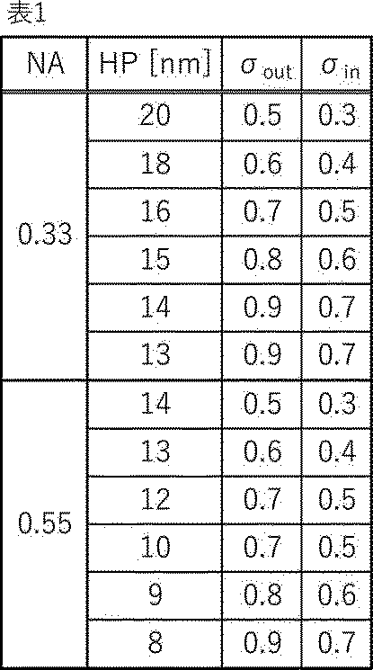
- simulations were performed assuming that the numerical aperture NA of the lens of the EUV exposure apparatus was 0.33, or 0.55 in consideration of a next-generation model aimed at further miniaturization of patterns.
- the second linear pattern corresponding to the second linear transfer pattern L2 is 4 times the HP of the CD, that is, the second line It was assumed that the HP of the transfer pattern was four times as large.
- the refractive index n was varied within the range of 0.88 to 0.96
- the extinction coefficient k was varied within the range of 0.015 to 0.065
- the film thickness d of the absorption layer was varied within the range of 20 to 80 nm.
- the line width and the incident surface of the exposure light I are perpendicular.
- the line width and the incident surface of the exposure light I are parallel.
- the reflective mask 20 satisfies all of the following formulas (1) to (3), where NILS of the first linear transfer pattern L1 is expressed as N V and NILS of the second linear transfer pattern L2 is expressed as N H. It is preferable to meet the requirements.
- N V and N H are, the more preferable they are, and from the viewpoint of good contrast of the transferred pattern, both are preferably 2.80 or more, more preferably 2.85 or more.
- FIG. 5(a) is a distribution diagram in which the lower value of N V or N H , that is, min ⁇ N V , N H ⁇ is expressed by contour lines. This means that both N V and N H are greater than or equal to the NILS value represented by the contour lines.
- d optimal value
- FIG. 5(b) shows the phase difference calculated from the values of d, n, and k at this time using contour lines.
- phase difference at which NILS reaches its maximum value increases when the value of HP is small is considered as follows.
- the electric field of light changes continuously at the boundary between spaces and lines (unevenness) of the mask pattern.
- the continuous period of the unevenness of the mask pattern becomes shorter, and accordingly, the period of the electric field of light at the boundary between the unevenness of the mask pattern becomes shorter than when the value of HP is large.
- the value of HP is comparable to or smaller than the wavelength of EUV exposure light (13.5 nm)
- the distortion of the electric field in the mask pattern becomes large, and as a result, the actual distortion of the spaces and lines of the mask pattern increases.
- the NILS differs depending on the direction of the linear transfer pattern, it becomes necessary to adjust and design the HP for each line direction of the mask pattern. Therefore, from the viewpoint of ease of designing a mask pattern, it is preferable that the difference in NILS values is small regardless of the line direction. In other words, it can be said that the smaller the difference between N V and N H , the more the transfer pattern can be formed with higher dimensional accuracy regardless of the direction of the linear pattern. From this point of view, as shown in equation (3), the ratio of the difference expressed by
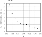
- FIG. 7 shows the relationship between k and
- N H is the NILS when the incident plane of the exposure light I is parallel to the line width direction (see FIG. 2(b)), and a part of the exposure light I incident on the mask pattern is in the space of the mask pattern ( The side wall of the recess) is irradiated. Furthermore, a portion of the reflected light from the multilayer reflective film 2 is also absorbed by the sidewalls of the recesses of the mask pattern.
- the phase difference ⁇ , NILS, when the transfer pattern (LS pattern) by EUV lithography has a predetermined HP Tables 3 and 4 show the optical simulation results for the total thickness d (optimal value) of the absorption layer 3.
- the values shown in Table 2 are used for the optical constants (n, k) of each metal element, and the composition of each alloy is Pd 0.79 Cr 0.21 , Ir 0.25 Mo 0.75 , Os 0.14 Ru 0.86 , Ru 0.5 Pt 0.5 , Ru 0.3 Ta 0.7 , Ru 0.55 Ir 0.45 , Os 0.6 Re 0 .4 .
- the optical constants of the alloy are also affected by the density and film forming conditions, so representative values were used.
- Ir/Ta 2 O 5 (10 nm) in Table 3 means that the absorption film 3 has two layers, the first layer from the substrate 1 side is an Ir film, and the second layer is a Ta 2 O 5 film (thickness 10 nm). It means that it is made of structure.
- the reflective mask 20 can be manufactured by forming a mask pattern M using the reflective mask blank 10 by applying a known lithography technique. For example, a photoresist film is formed on the absorption layer 3 of the reflective mask blank 10, processed into a resist pattern having a desired pattern shape, and after etching the absorption layer 3 by dry etching or the like, the resist pattern is By removing unnecessary photoresist including , a reflective mask 20 in which a mask pattern M is formed on the absorption layer 3 can be obtained.
- Substrate 2 Multilayer reflective film 3
- Absorption layer 4 Protective film 10
- Reflective mask blank 20 Reflective mask I Exposure light
- First linear transfer pattern L2 Second linear transfer pattern T Transferred surface M Mask pattern
Landscapes
- Physics & Mathematics (AREA)
- General Physics & Mathematics (AREA)
- Preparing Plates And Mask In Photomechanical Process (AREA)
- Exposure Of Semiconductors, Excluding Electron Or Ion Beam Exposure (AREA)
Abstract
Description
透過型の位相シフトマスクの一種であるハーフトーン型マスクは、透過光の位相を変化させる部分に、露光光に対する半透過性の薄膜が形成されている。ハーフトーン型マスクは、透過率を数%程度(通常、基板透過光に対して2.5~15.0%程度)まで減衰させつつ、位相を変化させて、パターンエッジ部の解像度を向上させることにより、転写精度を向上させることができる。
なお、位相差は、原理上、180°が最良であるが、実質的に175~185°程度であれば、解像度の向上効果が得られることが知られている。
このため、従来の反射型マスクにおける位相シフトマスクは、位相差が180°前後(ほぼ反転)となるように設計されることが一般的であった(例えば、特許文献1参照)。
特に、LSIのパターンは、集積密度の上昇に伴って複雑化が進み、直交するライン状のパターンが複雑に入り組んだ構造を有しており、マスクパターンもこのような複雑な構造に対応する必要がある。
[1]基板上に、EUV光を反射する多層反射膜と、EUV光を吸収する吸収層とが、この順に前記基板側から積層されたEUVリソグラフィ用反射型マスクブランクであって、前記吸収層は、波長13.5nmのEUV光の屈折率が0.930以下、かつ、消衰係数が0.025以上であり、波長13.5nmのEUV光の入射光に対する、前記多層反射膜の表面からの反射光と前記吸収層の表面からの反射光との位相差が、220~280°である、反射型マスクブランク。
[2]前記位相差が、225~280°である、[1]に記載の反射型マスクブランク。
[3]前記吸収層に、互いのライン方向が直交する第1のライン状パターン及び第2のライン状パターンを含むマスクパターンを形成する、[1]又は[2]に記載の反射型マスクブランク。
[4]前記第1のライン状パターン及び前記第2のライン状パターンにより形成される転写パターンのハーフピッチが16nm以下である、[3]に記載の反射型マスクブランク。
[5]前記吸収層は、イリジウム(Ir)、レニウム(Re)、オスミウム(Os)、ルテニウム(Ru)、白金(Pt)、パラジウム(Pd)、金(Au)及び銀(Ag)から選ばれる1種以上の金属元素を含む、[1]~[4]のいずれかに記載の反射型マスクブランク。
[6]前記吸収層は、白金(Pt)、パラジウム(Pd)、金(Au)及び銀(Ag)から選ばれる1種以上の金属元素を含む、[1]~[4]のいずれかに記載の反射型マスクブランク。
[7]前記吸収層は、波長13.5nmのEUV光の消衰係数が0.025~0.040である、[1]~[6]のいずれかに記載の反射型マスクブランク。
[8]前記吸収層は、2層以上の膜が積層されてなる、[1]~[7]のいずれかに記載の反射型マスクブランク。
[9]前記吸収層は、総厚さが60nm以下である、[1]~[8]のいずれかに記載の反射型マスクブランク。
[10]前記多層反射膜と前記吸収層との間に、前記多層反射膜を保護する保護膜が形成されている、[1]~[9]のいずれかに記載の反射型マスクブランク。
[12]前記位相差が、225~280°である、[11]に記載の反射型マスク。
[13]前記マスクパターンが、互いのライン方向が直交する第1のライン状パターン及び第2のライン状パターンを含む、[11]又は[12]に記載の反射型マスク。
[14]露光光の入射面がライン幅に垂直であるライン状パターンの規格化像ログスロープをNV、露光光の入射面がライン幅に平行であるライン状パターンの規格化像ログスロープをNHと表したとき、下記式(1)~(3)のすべてを満たす、[13]に記載の反射型マスク。
NV≧2.80 (1)
NH≧2.80 (2)
|NV-NH|/min{NV,NH}<0.060 (3)
[15]前記反射型マスクの第1のライン状パターン及び第2のライン状パターンにより形成される転写パターンのハーフピッチが16nm以下である、[13]又は[14]に記載の反射型マスク。
[16]前記吸収層は、イリジウム(Ir)、レニウム(Re)、オスミウム(Os)、ルテニウム(Ru)、白金(Pt)、パラジウム(Pd)、金(Au)及び銀(Ag)から選ばれる1種以上の金属元素を含む、[11]~[15]のいずれかに記載の反射型マスク。
[17]前記吸収層は、白金(Pt)、パラジウム(Pd)、金(Au)及び銀(Ag)から選ばれる1種以上の金属元素を含む、[11]~[15]のいずれかに記載の反射型マスク。
[18]前記吸収層は、波長13.5nmのEUV光の消衰係数が0.025~0.040である、[11]~[17]のいずれかに記載の反射型マスク。
基板上、層上及び膜上(以下、膜等上と略称する。)とは、膜等の上面に接する場合のみならず、膜等の上面に接していない上方も含む意味である。例えば、「膜A上の膜B」とは、膜Aと膜Bとが接していてもよく、膜Aと膜Bとの間に他の膜等が介在していてもよい。また、ここで言う「上」とは、必ずしも鉛直方向における高い位置を意味する場合に限られず、相対的な位置関係を示すものである。
成膜した膜等の厚さは、透過型電子顕微鏡やX線反射率法により測定できる。
好ましい数値範囲は、好ましい下限値及び上限値のそれぞれを任意に組み合わせることができる。
以下、本発明の実施形態について、図面を参照して説明する。
図1に、本実施形態の反射型マスクブランクの断面を模式的に示す。図1に示す反射型マスクブランク10は、基板1上に、EUV光を反射する多層反射膜2と、EUV光を吸収する吸収層3とが、この順に基板1側から積層されている。
多層反射膜2と吸収層3との間には、マスクパターンを形成する際のドライエッチングから多層反射膜2を保護する保護膜4(キャップ層とも呼ばれる。)が形成されていてもよい。さらに、マスク加工後のパターン欠陥検査を容易にするための反射防止膜(図示せず)が、吸収層3上に形成され得る。
基板1は、EUV露光時の熱による転写パターンの歪み防止の観点から、20℃における熱膨張係数が低いことが好ましく、好ましくは0±0.05×10⁻⁷/℃、より好ましくは0±0.03×10-7/℃である。また、基板1は、平滑性に優れ、平坦度が高く、かつ、反射型マスクの製造プロセスで使用される洗浄液への耐性(耐薬品性)に優れていることが好ましい。
基板1の材料としては、例えば、SiO2-TiO2系ガラス、多成分系ガラスセラミックス等が挙げられ、また、β-石英固溶体が析出した結晶化ガラス、石英ガラス、シリコン、金属等も使用できる。
多層反射膜2は、EUV光の反射率を高くする観点から、屈折率が異なる元素を主成分とする複数の層を周期的に積層させた構成であることが好ましい。一般に、多層反射膜2は、高屈折率層1層と低屈折率層1層との組を1周期とし、40~60周期程度積層された構造を有する。
高屈折率層/低屈折率層としては、Mo/Si多層反射膜が一般的であるが、これに限定されるものではなく、例えば、Ru/Si多層反射膜、Mo/Be多層反射膜、Mo化合物/Si化合物多層反射膜、Si/Mo/Ru多層反射膜、Si/Mo/Ru/Mo多層反射膜、MoRu/Si多層反射膜、Si/Ru/Mo多層反射膜、Si/Ru/Mo/Ru多層反射膜等も挙げられる。
多層反射膜2を構成する各膜の厚さ及び積層の繰り返し周期は、膜材料及びEUV光の所望の反射率等に応じて適宜設定される。
例えば、イオンビームスパッタ法で、Mo/Si多層反射膜を形成する場合、アルゴン(Ar)ガス(ガス圧1.3×10-2~2.7×10-2Pa)をスパッタガスとして、イオン加速電圧300~1500V、成膜速度0.030~0.300nm/secで、まず、Siターゲットを用いて、厚さ4.5nmになるようにSi膜を成膜し、次に、Moターゲットを用いて、厚さ2.3nmになるようにMo膜を成膜する。これを1周期として、Mo膜/Si膜を30~60周期繰り返して積層させることにより、Mo/Si多層反射膜を形成できる。
多層反射膜2と吸収層3との間には、マスクパターンを形成する際のドライエッチングから多層反射膜2を保護する保護膜4が形成されていてもよい。保護膜4は、EUV露光時に多層反射膜2が酸化して、EUV光の反射率が低下することを防止する役割も有する。
なお、エッチングガスとしては、通常、ハロゲン系ガス、酸素系ガス、又はこれらの混合ガスが用いられる。ハロゲン系ガスとしては、例えば、Cl2、SiCl4、CHCl3、CCl4及びBCl3から選ばれる1種以上を含む塩素系ガス;CF4、CHF3、SF6、BF3及びXeF2から選ばれる1種以上を含むフッ素系ガスが挙げられる。
同様の観点から、保護膜4は、二乗平均粗さ(RMS)が、好ましくは0.3nm以下、より好ましくは0.1nm以下であり、平滑であることが好ましい。
吸収層3は、波長13.5nmのEUV光の屈折率が0.930以下、かつ、消衰係数が0.025以上であり、波長13.5nmのEUV光の入射光に対する、多層反射膜2の表面からの反射光と吸収層3の表面からの反射光との位相差が、220~280°となるように形成される。
本実施形態の反射型マスクブランクは、吸収層3が、このような特性を有していることにより、微細なライン状パターンを高い寸法精度で転写できるEUVリソグラフィ用反射型マスクに好適である。
屈折率が上記範囲内であることにより、位相差を大きくしやすく、微細なライン状パターンを高い寸法精度で転写できる位相シフトマスクが得られる。
消衰係数が上記範囲内であることにより、微細なライン状パターンを高い寸法精度で転写できる位相シフトマスクが得られる。
上記範囲内の位相差であることにより、微細なライン状パターンを高い寸法精度で転写できる位相シフトマスクが得られる。
なお、本発明において、位相シフトマスクにおける多層反射膜2からの反射光とは、吸収層3を透過することなく、マスクパターンの開口部を通過し、(保護膜4及び)多層反射膜2に直接入射した波長13.5nmのEUV光が、多層反射膜2で反射され、再び吸収層3を透過することなく、マスクパターンの開口部を通過した反射光を意味する。また、吸収層3の表面からの反射光とは、波長13.5nmのEUV光の入射光が、吸収層3で吸収されながら吸収層3(及び保護膜4)を透過し、多層反射膜2で反射され、再び吸収層3で吸収されながら吸収層3を透過した反射光を意味する。
式(4)中、θは位相差、dは吸収層3の膜厚、λは入射光の波長、nは吸収層3の屈折率である。
本発明では、λ=13.5[nm]、n<1であることから、吸収層3は、膜厚が薄く、屈折率が大きいほど、位相差は小さくなる。
図2(a)及び(b)に示す被転写面T上の第1のライン状転写パターンL1及び第2のライン状転写パターンL2は、いずれも、ラインの幅と間隔とがいずれも等しいが、幅及び間隔のそれぞれ、また、幅と間隔とが異なっていてもよい。また、ライン同士が交差する部分を含んでいてもよい。
上記範囲内のHPである場合に、寸法精度が高い位相シフトマスクとしてのより優れた効果が得られる。
EUVリソグラフィは縮小投影露光であり、マスクパターンに対する転写パターンの縮小率は、通常、4倍であるため、例えば、転写パターンが、HPが16nmのライン幅とライン間隔が等しいLSパターンである場合、マスクパターンは、HPが64nmのLSパターンとなる。
なお、ライン幅とライン間隔が異なるLSパターンの場合は、解像限界におけるライン幅の限界寸法(CD;Critical Dimension)を、HPに相当するものとみなすことができる。
複層構成の場合の屈折率及び消衰係数は、各層の屈折率及び消衰係数の各厚さを加味した加重平均値として求められる。
吸収層3上には、検査工程で波長190~260nmのDUV光(深紫外光)を使用する場合、反射を防止する反射防止膜(図示せず)が積層されていてもよい。
反射型マスクは、吸収層3に形成されたマスクパターンの欠陥を調べるマスク検査が行われることがある。このマスク検査は、主に検査光の反射光の光学データに基づいて、欠陥の有無等が判断されることから、マスクを透過する光は検査光として使用できず、DUV光が用いられる。正確な検査の観点から、吸収層3上には、検査光であるDUV光の反射を防止する反射防止膜を設けておくことが好ましい。
本実施形態の反射型マスクブランクは、上述した各膜及び層以外に、反射型マスクブランクにおいて公知の機能膜を設けてもよい。
例えば、反射型マスクブランク10を静電チャックの載置部等に吸着固定させるために、基板1の多層反射膜2とは反対側の面(裏面)に、裏面導電膜が形成されていてもよい。
裏面導電膜は、シート抵抗が100Ω/□以下であることが好ましく、公知の構成を適用することができる。裏面導電膜の構成材料としては、例えば、Si、TiN、Mo、Cr、TaSi等が挙げられる。裏面導電膜の厚さは、例えば、10~1000nmとすることができる。
裏面導電膜は、例えば、マグネトロンスパッタ法、イオンビームスパッタ法、化学気相成長法(CVD法)、真空蒸着法、電気メッキ法等の公知の成膜方法を用いて、所望の厚さで成膜することにより形成できる。
図3に、本実施形態の反射型マスクの断面を模式的に示す。図3に示す反射型マスク20は、基板1上に、EUV光を反射する多層反射膜2と、EUV光を吸収する吸収層3とが、この順に基板1側から積層されたEUVリソグラフィ用反射型マスクであって、吸収層3は、波長13.5nmのEUV光の屈折率が0.95以下、かつ、消衰係数が0.025以上であり、波長13.5nmのEUV光の入射光に対する、多層反射膜2の表面からの反射光と吸収層3の表面からの反射光との位相差が、220~280°、好ましくは225~280°であり、吸収層3にマスクパターンMが形成されているものである。
すなわち、本発明の反射型マスクは、本実施形態の反射型マスクブランク10の吸収層3にマスクパターンMが形成されているものである。したがって、反射型マスク20の各構成層の説明は、上記の反射型マスクブランク10についての説明と同様であるため、省略する。
上記範囲内のHPのライン状パターンを含む場合に、転写精度が高い位相シフトマスクとしてのより優れた効果が得られる。

NA=0.33の場合、マスクパターンの縮小倍率は、縦横とも4倍であり、反射型マスク20の吸収層3に形成される第1のライン状パターン及び第2のライン状パターンはいずれも、CDの4倍、すなわち、転写パターンのLSパターンのHPの4倍と仮定した。
NA=0.55の場合、マスクパターンの縮小倍率は縦(スキャン方向)8倍、横4倍であり、第1のライン状転写パターンL1に対応する第1のライン状パターンは、CDの8倍、すなわち、第1のライン状転写パターンのHPの8倍と仮定し、第2のライン状転写パターンL2に対応する第2のライン状パターンは、CDの4倍、すなわち、第2のライン状転写パターンのHPの4倍と仮定した。
<NA=0.33の場合>
EUV露光光:λ=13.5[nm]、入射角6°
マスクパターンの縮小倍率:縦横とも4倍
HP(=CD)=13~20[nm]
照明系:二重極照明;各HPにおけるコヒーレンスファクターσout及びσinの最適値を表1に示す。
EUV露光光:λ=13.5[nm]、入射角5.355°
マスクスパターンの縮小倍率:縦8倍、横4倍
HP(=CD)=8~14[nm]
照明系:二重極照明;各HPにおけるコヒーレンスファクターσout及びσinの最適値を表1に示す。
NV≧2.80 (1)
NH≧2.80 (2)
|NV-NH|/min{NV,NH}<0.060 (3)
HP=20[nm]の場合は、図5(a)から、nが低く、かつ、kが高いほどNILSが高いが、図5(b)から、このときの好ましい位相差は、公知のとおり、180~216°程度の範囲内であると言える。
HP=12[nm]の場合は、図6(a)から、n≦0.930、かつ、k≧0.025の範囲で、NILS≧2.80以上となり、また、図6(b)から、このときの位相差は、220~280°の範囲内であることが確認された。
LSパターンの反射型マスクでは、マスクパターンのスペースとライン(凹凸)の境界部で、光の電界が連続的に変化する。HPの値が小さくなると、マスクパターンの凹凸の連続周期が短くなり、これに伴い、マスクパターンの凹凸の境界部での光の電界は、HPの値が大きい場合に比べて、周期が短くなる。すなわち、HPの値が、EUV露光光の波長(13.5nm)と同等程度又はより小さい場合は、マスクパターンにおける電界の歪みが大きくなり、結果的に、マスクパターンのスペースとラインとでの実際の位相差は、狙いよりも小さくなる現象が生じると考えられる。このため、HPの値が小さい場合には、予め吸収層3の厚さの調整等により、より大きな位相差を生じるように作製されたマスクブランクを用いることにより、位相シフトマスクの効果を実現できる。
また、kの値が低くなると、NHが低くなる要因として、以下の点も挙げられる。NHは、露光光Iの入射面がライン幅方向と平行であるとき(図2(b)参照)のNILSであり、マスクパターンへ入射する露光光Iの一部は、マスクパターンのスペース(凹部)の側壁に対して照射される。また、多層反射膜2からの反射光の一部も、マスクパターンの凹部の側壁に吸収される。このため、NHは、マスクパターンの凹凸構造によるシャドーイングの影響を受けて低下し、第2のライン状の転写パターンL2の方が、第1のライン状の転写パターンL1よりも、寸法精度が劣る傾向がある。
したがって、kの値が高ければ、吸収層3における光吸収が大きくなり、シャドーイングによる散乱光の発生等の影響を抑制できる。
NA=0.55の場合でも、同様な結果が得られる。
なお、表3及び4に示す吸収層3において、各金属元素の光学定数(n、k)は、表2に示す値を用い、各合金の組成は、Pd0.79Cr0.21、Ir0.25Mo0.75、Os0.14Ru0.86、Ru0.5Pt0.5、Ru0.3Ta0.7、Ru0.55Ir0.45、Os0.6Re0.4とした。合金の光学定数は、厳密には、密度や製膜条件の影響も受けるため、代表値を用いた。また、表3のIr/Ta2O5(10nm)とは、吸収膜3が、基板1側から1層目がIr膜、2層目がTa2O5膜(厚さ10nm)の2層構造で形成されていることを意味する。

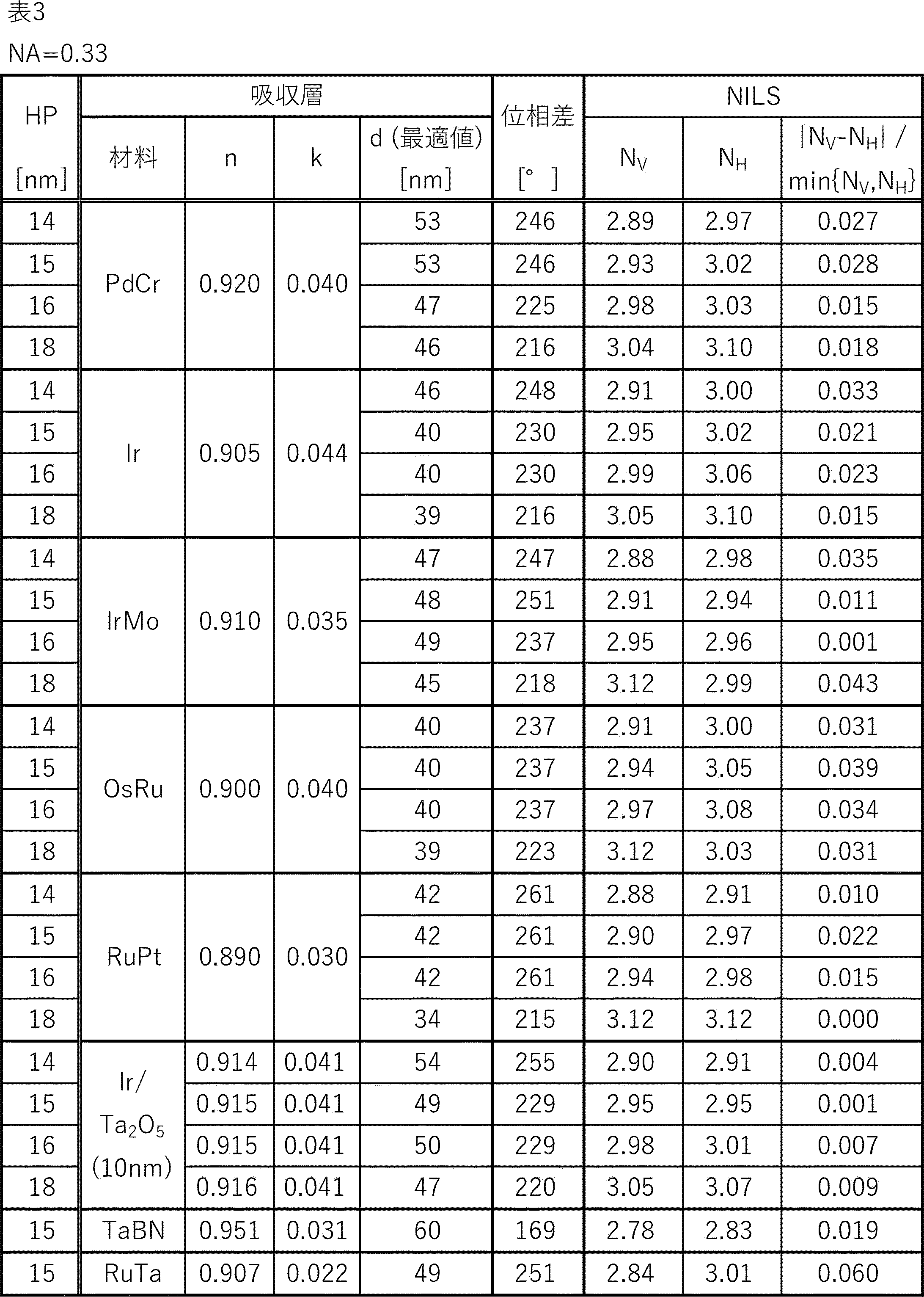
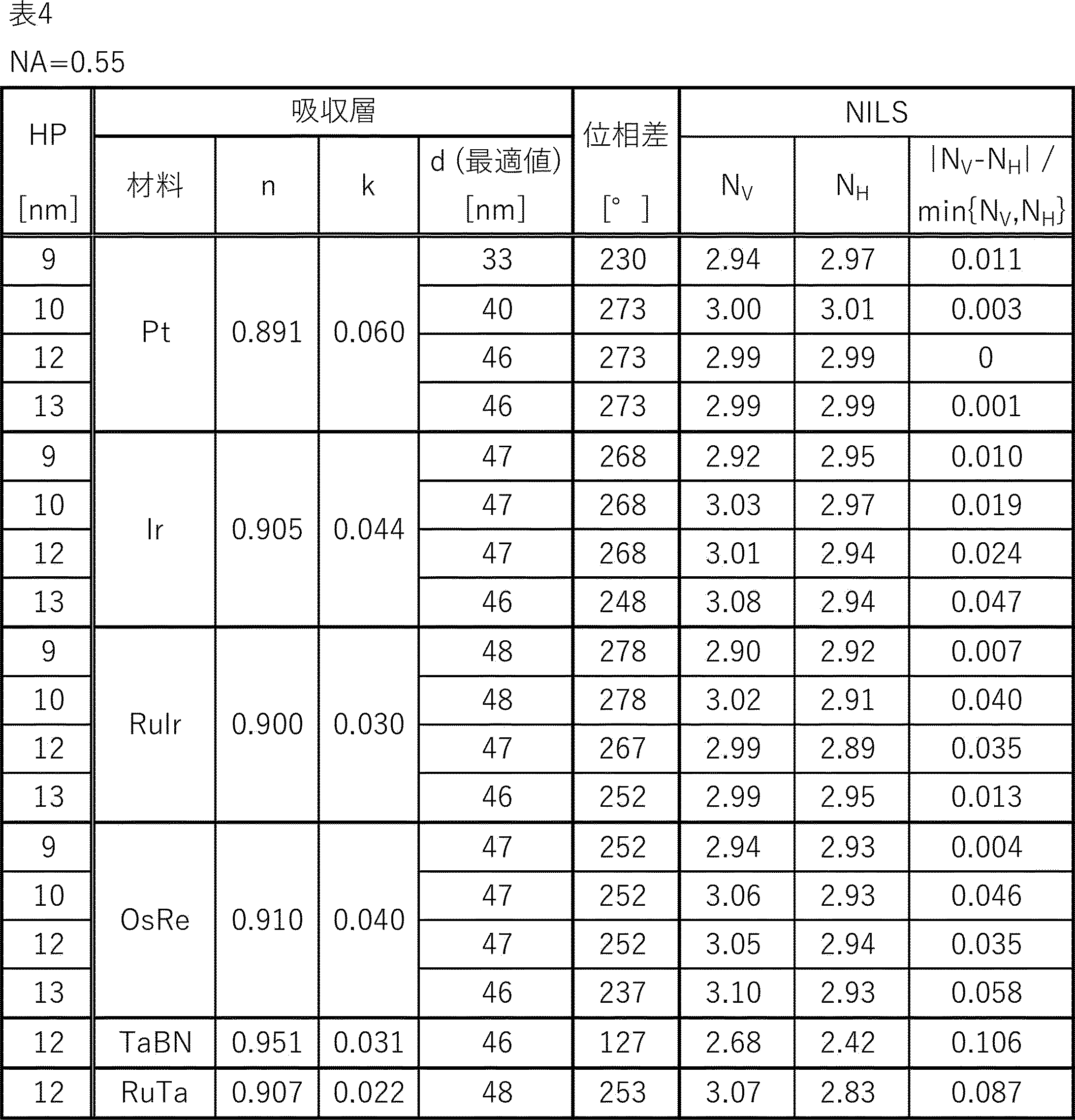
また、屈折率が0.930以下、かつ、消衰係数が0.025以上であっても、転写パターンのHPが18nmのときは、位相差が220°未満でも、NV及びNHが高い場合もある。一方、HPが16nm以下のときは、位相差が220~280°で、層厚さ60nm以下でも、寸法精度が高い転写パターンが得られると言える。
2 多層反射膜
3 吸収層
4 保護膜
10 反射型マスクブランク
20 反射型マスク
I 露光光
L1 第1のライン状転写パターン
L2 第2のライン状転写パターン
T 被転写面
M マスクパターン
Claims (18)
- 基板上に、EUV光を反射する多層反射膜と、EUV光を吸収する吸収層とが、この順に前記基板側から積層されたEUVリソグラフィ用反射型マスクブランクであって、
前記吸収層は、波長13.5nmのEUV光の屈折率が0.930以下、かつ、消衰係数が0.025以上であり、
波長13.5nmのEUV光の入射光に対する、前記多層反射膜の表面からの反射光と前記吸収層の表面からの反射光との位相差が、220~280°である、
反射型マスクブランク。 - 前記位相差が、225~280°である、請求項1に記載の反射型マスクブランク。
- 前記吸収層に、互いのライン方向が直交する第1のライン状パターン及び第2のライン状パターンを含むマスクパターンを形成する、請求項1又は2に記載の反射型マスクブランク。
- 前記第1のライン状パターン及び前記第2のライン状パターンにより形成される転写パターンのハーフピッチが16nm以下である、請求項3に記載の反射型マスクブランク。
- 前記吸収層は、イリジウム(Ir)、レニウム(Re)、オスミウム(Os)、ルテニウム(Ru)、白金(Pt)、パラジウム(Pd)、金(Au)及び銀(Ag)から選ばれる1種以上の金属元素を含む、請求項1又は2に記載の反射型マスクブランク。
- 前記吸収層は、白金(Pt)、パラジウム(Pd)、金(Au)及び銀(Ag)から選ばれる1種以上の金属元素を含む、請求項1又は2に記載の反射型マスクブランク。
- 前記吸収層は、波長13.5nmのEUV光の消衰係数が0.025~0.040である、請求項1又は2に記載の反射型マスクブランク。
- 前記吸収層は、2層以上の膜が積層されてなる、請求項1又は2に記載の反射型マスクブランク。
- 前記吸収層は、総厚さが60nm以下である、請求項1又は2に記載の反射型マスクブランク。
- 前記多層反射膜と前記吸収層との間に、前記多層反射膜を保護する保護膜が形成されている、請求項1又は2に記載の反射型マスクブランク。
- 基板上に、EUV光を反射する多層反射膜とEUV光を吸収する吸収層とが、この順に前記基板側から積層されたEUVリソグラフィ用反射型マスクであって、
前記吸収層は、波長13.5nmのEUV光の屈折率が0.930以下、かつ、消衰係数が0.025以上であり、
波長13.5nmのEUV光の入射光に対する、前記多層反射膜の表面からの反射光と前記吸収層の表面からの反射光との位相差が、220~280°であり、
前記吸収層にマスクパターンが形成されている、
反射型マスク。 - 前記位相差が、225~280°である、請求項11に記載の反射型マスク。
- 前記マスクパターンが、互いのライン方向が直交する第1のライン状パターン及び第2のライン状パターンを含む、請求項11又は12に記載の反射型マスク。
- 露光光の入射面がライン幅に垂直であるライン状パターンの規格化像ログスロープをNV、露光光の入射面がライン幅に平行であるライン状パターンの規格化像ログスロープをNHと表したとき、下記式(1)~(3)のすべてを満たす、請求項13に記載の反射型マスク。
NV≧2.80 (1)
NH≧2.80 (2)
|NV-NH|/min{NV,NH}<0.060 (3) - 前記反射型マスクの第1のライン状パターン及び第2のライン状パターンにより形成される転写パターンのハーフピッチが16nm以下である、請求項13に記載の反射型マスク。
- 前記吸収層は、イリジウム(Ir)、レニウム(Re)、オスミウム(Os)、ルテニウム(Ru)、白金(Pt)、パラジウム(Pd)、金(Au)及び銀(Ag)から選ばれる1種以上の金属元素を含む、請求項11又は12に記載の反射型マスク。
- 前記吸収層は、白金(Pt)、パラジウム(Pd)、金(Au)及び銀(Ag)から選ばれる1種以上の金属元素を含む、請求項11又は12に記載の反射型マスク。
- 前記吸収層は、波長13.5nmのEUV光の消衰係数が0.025~0.040である、請求項11又は12に記載の反射型マスク。
Priority Applications (3)
| Application Number | Priority Date | Filing Date | Title |
|---|---|---|---|
| JP2024539093A JPWO2024029409A1 (ja) | 2022-08-03 | 2023-07-25 | |
| KR1020257002975A KR20250041128A (ko) | 2022-08-03 | 2023-07-25 | 반사형 마스크 블랭크 및 반사형 마스크 |
| US19/026,233 US20250172863A1 (en) | 2022-08-03 | 2025-01-16 | Reflective mask blank and reflective mask |
Applications Claiming Priority (2)
| Application Number | Priority Date | Filing Date | Title |
|---|---|---|---|
| JP2022-124350 | 2022-08-03 | ||
| JP2022124350 | 2022-08-03 |
Related Child Applications (1)
| Application Number | Title | Priority Date | Filing Date |
|---|---|---|---|
| US19/026,233 Continuation US20250172863A1 (en) | 2022-08-03 | 2025-01-16 | Reflective mask blank and reflective mask |
Publications (1)
| Publication Number | Publication Date |
|---|---|
| WO2024029409A1 true WO2024029409A1 (ja) | 2024-02-08 |
Family
ID=89849014
Family Applications (1)
| Application Number | Title | Priority Date | Filing Date |
|---|---|---|---|
| PCT/JP2023/027271 Ceased WO2024029409A1 (ja) | 2022-08-03 | 2023-07-25 | 反射型マスクブランク及び反射型マスク |
Country Status (5)
| Country | Link |
|---|---|
| US (1) | US20250172863A1 (ja) |
| JP (1) | JPWO2024029409A1 (ja) |
| KR (1) | KR20250041128A (ja) |
| TW (1) | TW202411766A (ja) |
| WO (1) | WO2024029409A1 (ja) |
Citations (5)
| Publication number | Priority date | Publication date | Assignee | Title |
|---|---|---|---|---|
| JP2020106639A (ja) * | 2018-12-27 | 2020-07-09 | Hoya株式会社 | 反射型マスクブランク、反射型マスク、及び半導体装置の製造方法 |
| WO2021085382A1 (ja) * | 2019-10-29 | 2021-05-06 | Agc株式会社 | 反射型マスクブランクおよび反射型マスク |
| WO2021132111A1 (ja) * | 2019-12-27 | 2021-07-01 | Agc株式会社 | Euvリソグラフィ用反射型マスクブランク、euvリソグラフィ用反射型マスク、およびそれらの製造方法 |
| JP2022003417A (ja) * | 2017-07-05 | 2022-01-11 | 凸版印刷株式会社 | 反射型フォトマスクブランク及び反射型フォトマスク |
| WO2023095769A1 (ja) * | 2021-11-24 | 2023-06-01 | 株式会社トッパンフォトマスク | 反射型フォトマスクブランク及び反射型フォトマスク |
Family Cites Families (1)
| Publication number | Priority date | Publication date | Assignee | Title |
|---|---|---|---|---|
| JP5766393B2 (ja) | 2009-07-23 | 2015-08-19 | 株式会社東芝 | 反射型露光用マスクおよび半導体装置の製造方法 |
-
2023
- 2023-07-25 KR KR1020257002975A patent/KR20250041128A/ko active Pending
- 2023-07-25 WO PCT/JP2023/027271 patent/WO2024029409A1/ja not_active Ceased
- 2023-07-25 JP JP2024539093A patent/JPWO2024029409A1/ja active Pending
- 2023-07-28 TW TW112128416A patent/TW202411766A/zh unknown
-
2025
- 2025-01-16 US US19/026,233 patent/US20250172863A1/en active Pending
Patent Citations (5)
| Publication number | Priority date | Publication date | Assignee | Title |
|---|---|---|---|---|
| JP2022003417A (ja) * | 2017-07-05 | 2022-01-11 | 凸版印刷株式会社 | 反射型フォトマスクブランク及び反射型フォトマスク |
| JP2020106639A (ja) * | 2018-12-27 | 2020-07-09 | Hoya株式会社 | 反射型マスクブランク、反射型マスク、及び半導体装置の製造方法 |
| WO2021085382A1 (ja) * | 2019-10-29 | 2021-05-06 | Agc株式会社 | 反射型マスクブランクおよび反射型マスク |
| WO2021132111A1 (ja) * | 2019-12-27 | 2021-07-01 | Agc株式会社 | Euvリソグラフィ用反射型マスクブランク、euvリソグラフィ用反射型マスク、およびそれらの製造方法 |
| WO2023095769A1 (ja) * | 2021-11-24 | 2023-06-01 | 株式会社トッパンフォトマスク | 反射型フォトマスクブランク及び反射型フォトマスク |
Also Published As
| Publication number | Publication date |
|---|---|
| TW202411766A (zh) | 2024-03-16 |
| KR20250041128A (ko) | 2025-03-25 |
| JPWO2024029409A1 (ja) | 2024-02-08 |
| US20250172863A1 (en) | 2025-05-29 |
Similar Documents
| Publication | Publication Date | Title |
|---|---|---|
| US12111566B2 (en) | Reflective mask blank, reflective mask and manufacturing method thereof, and semiconductor device manufacturing method | |
| TWI886176B (zh) | 反射型光罩基底及反射型光罩、以及半導體裝置之製造方法 | |
| JP7502510B2 (ja) | 反射型マスクブランク、反射型マスク、及び半導体装置の製造方法 | |
| KR102906466B1 (ko) | 반사형 마스크 블랭크, 반사형 마스크, 그리고 반사형 마스크 및 반도체 장치의 제조 방법 | |
| TWI881058B (zh) | 反射型光罩基底及反射型光罩、與半導體裝置之製造方法 | |
| KR102002441B1 (ko) | 반사형 마스크 블랭크, 반사형 마스크 및 그 제조 방법, 및 반도체 장치의 제조 방법 | |
| WO2017169658A1 (ja) | 反射型マスクブランク、反射型マスク及び半導体装置の製造方法 | |
| KR20160034315A (ko) | 다층 반사막을 구비한 기판, euv 리소그래피용 반사형 마스크 블랭크, euv 리소그래피용 반사형 마스크 및 그 제조 방법과 반도체 장치의 제조 방법 | |
| JP6441012B2 (ja) | 反射型マスクブランク、反射型マスク及びその製造方法、並びに半導体装置の製造方法 | |
| KR20160054458A (ko) | 다층 반사막을 구비한 기판, euv 리소그래피용 반사형 마스크 블랭크, euv 리소그래피용 반사형 마스크 및 그 제조 방법과 반도체 장치의 제조 방법 | |
| US20250172864A1 (en) | Reflective mask blank and reflective mask | |
| JP2020181206A (ja) | 反射型マスクブランク、反射型マスク及び半導体装置の製造方法 | |
| JP6855190B2 (ja) | 反射型マスク、並びに反射型マスクブランク及び半導体装置の製造方法 | |
| WO2023008435A1 (ja) | 反射型マスクブランク、反射型マスク、反射型マスクブランクの製造方法、及び反射型マスクの製造方法 | |
| US20250172863A1 (en) | Reflective mask blank and reflective mask |
Legal Events
| Date | Code | Title | Description |
|---|---|---|---|
| 121 | Ep: the epo has been informed by wipo that ep was designated in this application |
Ref document number: 23849964 Country of ref document: EP Kind code of ref document: A1 |
|
| WWE | Wipo information: entry into national phase |
Ref document number: 2024539093 Country of ref document: JP |
|
| ENP | Entry into the national phase |
Ref document number: 20257002975 Country of ref document: KR Kind code of ref document: A |
|
| WWE | Wipo information: entry into national phase |
Ref document number: 11202500496R Country of ref document: SG |
|
| WWP | Wipo information: published in national office |
Ref document number: 11202500496R Country of ref document: SG |
|
| NENP | Non-entry into the national phase |
Ref country code: DE |
|
| WWP | Wipo information: published in national office |
Ref document number: 1020257002975 Country of ref document: KR |
|
| 122 | Ep: pct application non-entry in european phase |
Ref document number: 23849964 Country of ref document: EP Kind code of ref document: A1 |