WO2024029329A1 - 高純度シリコンの積層造形方法、半導体製造装置用部品の積層造形方法、半導体製造装置用部品及び半導体製造装置用部品の形成方法 - Google Patents
高純度シリコンの積層造形方法、半導体製造装置用部品の積層造形方法、半導体製造装置用部品及び半導体製造装置用部品の形成方法 Download PDFInfo
- Publication number
- WO2024029329A1 WO2024029329A1 PCT/JP2023/026319 JP2023026319W WO2024029329A1 WO 2024029329 A1 WO2024029329 A1 WO 2024029329A1 JP 2023026319 W JP2023026319 W JP 2023026319W WO 2024029329 A1 WO2024029329 A1 WO 2024029329A1
- Authority
- WO
- WIPO (PCT)
- Prior art keywords
- semiconductor manufacturing
- silicon
- powder
- manufacturing equipment
- forming
- Prior art date
- Legal status (The legal status is an assumption and is not a legal conclusion. Google has not performed a legal analysis and makes no representation as to the accuracy of the status listed.)
- Ceased
Links
Images










Classifications
-
- B—PERFORMING OPERATIONS; TRANSPORTING
- B33—ADDITIVE MANUFACTURING TECHNOLOGY
- B33Y—ADDITIVE MANUFACTURING, i.e. MANUFACTURING OF THREE-DIMENSIONAL [3D] OBJECTS BY ADDITIVE DEPOSITION, ADDITIVE AGGLOMERATION OR ADDITIVE LAYERING, e.g. BY 3D PRINTING, STEREOLITHOGRAPHY OR SELECTIVE LASER SINTERING
- B33Y10/00—Processes of additive manufacturing
-
- H—ELECTRICITY
- H10—SEMICONDUCTOR DEVICES; ELECTRIC SOLID-STATE DEVICES NOT OTHERWISE PROVIDED FOR
- H10P—GENERIC PROCESSES OR APPARATUS FOR THE MANUFACTURE OR TREATMENT OF DEVICES COVERED BY CLASS H10
- H10P14/00—Formation of materials, e.g. in the shape of layers or pillars
- H10P14/60—Formation of materials, e.g. in the shape of layers or pillars of insulating materials
- H10P14/63—Formation of materials, e.g. in the shape of layers or pillars of insulating materials characterised by the formation processes
- H10P14/6326—Deposition processes
- H10P14/6328—Deposition from the gas or vapour phase
- H10P14/6334—Deposition from the gas or vapour phase using decomposition or reaction of gaseous or vapour phase compounds, i.e. chemical vapour deposition
- H10P14/6336—Deposition from the gas or vapour phase using decomposition or reaction of gaseous or vapour phase compounds, i.e. chemical vapour deposition in the presence of a plasma [PECVD]
-
- B—PERFORMING OPERATIONS; TRANSPORTING
- B22—CASTING; POWDER METALLURGY
- B22F—WORKING METALLIC POWDER; MANUFACTURE OF ARTICLES FROM METALLIC POWDER; MAKING METALLIC POWDER; APPARATUS OR DEVICES SPECIALLY ADAPTED FOR METALLIC POWDER
- B22F1/00—Metallic powder; Treatment of metallic powder, e.g. to facilitate working or to improve properties
- B22F1/05—Metallic powder characterised by the size or surface area of the particles
-
- B—PERFORMING OPERATIONS; TRANSPORTING
- B22—CASTING; POWDER METALLURGY
- B22F—WORKING METALLIC POWDER; MANUFACTURE OF ARTICLES FROM METALLIC POWDER; MAKING METALLIC POWDER; APPARATUS OR DEVICES SPECIALLY ADAPTED FOR METALLIC POWDER
- B22F10/00—Additive manufacturing of workpieces or articles from metallic powder
- B22F10/20—Direct sintering or melting
- B22F10/28—Powder bed fusion, e.g. selective laser melting [SLM] or electron beam melting [EBM]
-
- B—PERFORMING OPERATIONS; TRANSPORTING
- B22—CASTING; POWDER METALLURGY
- B22F—WORKING METALLIC POWDER; MANUFACTURE OF ARTICLES FROM METALLIC POWDER; MAKING METALLIC POWDER; APPARATUS OR DEVICES SPECIALLY ADAPTED FOR METALLIC POWDER
- B22F10/00—Additive manufacturing of workpieces or articles from metallic powder
- B22F10/30—Process control
- B22F10/36—Process control of energy beam parameters
-
- B—PERFORMING OPERATIONS; TRANSPORTING
- B22—CASTING; POWDER METALLURGY
- B22F—WORKING METALLIC POWDER; MANUFACTURE OF ARTICLES FROM METALLIC POWDER; MAKING METALLIC POWDER; APPARATUS OR DEVICES SPECIALLY ADAPTED FOR METALLIC POWDER
- B22F10/00—Additive manufacturing of workpieces or articles from metallic powder
- B22F10/80—Data acquisition or data processing
- B22F10/85—Data acquisition or data processing for controlling or regulating additive manufacturing processes
-
- B—PERFORMING OPERATIONS; TRANSPORTING
- B22—CASTING; POWDER METALLURGY
- B22F—WORKING METALLIC POWDER; MANUFACTURE OF ARTICLES FROM METALLIC POWDER; MAKING METALLIC POWDER; APPARATUS OR DEVICES SPECIALLY ADAPTED FOR METALLIC POWDER
- B22F12/00—Apparatus or devices specially adapted for additive manufacturing; Auxiliary means for additive manufacturing; Combinations of additive manufacturing apparatus or devices with other processing apparatus or devices
- B22F12/10—Auxiliary heating means
- B22F12/17—Auxiliary heating means to heat the build chamber or platform
-
- B—PERFORMING OPERATIONS; TRANSPORTING
- B28—WORKING CEMENT, CLAY, OR STONE
- B28B—SHAPING CLAY OR OTHER CERAMIC COMPOSITIONS; SHAPING SLAG; SHAPING MIXTURES CONTAINING CEMENTITIOUS MATERIAL, e.g. PLASTER
- B28B1/00—Producing shaped prefabricated articles from the material
- B28B1/001—Rapid manufacturing of 3D objects by additive depositing, agglomerating or laminating of material
-
- B—PERFORMING OPERATIONS; TRANSPORTING
- B33—ADDITIVE MANUFACTURING TECHNOLOGY
- B33Y—ADDITIVE MANUFACTURING, i.e. MANUFACTURING OF THREE-DIMENSIONAL [3D] OBJECTS BY ADDITIVE DEPOSITION, ADDITIVE AGGLOMERATION OR ADDITIVE LAYERING, e.g. BY 3D PRINTING, STEREOLITHOGRAPHY OR SELECTIVE LASER SINTERING
- B33Y30/00—Apparatus for additive manufacturing; Details thereof or accessories therefor
-
- B—PERFORMING OPERATIONS; TRANSPORTING
- B33—ADDITIVE MANUFACTURING TECHNOLOGY
- B33Y—ADDITIVE MANUFACTURING, i.e. MANUFACTURING OF THREE-DIMENSIONAL [3D] OBJECTS BY ADDITIVE DEPOSITION, ADDITIVE AGGLOMERATION OR ADDITIVE LAYERING, e.g. BY 3D PRINTING, STEREOLITHOGRAPHY OR SELECTIVE LASER SINTERING
- B33Y40/00—Auxiliary operations or equipment, e.g. for material handling
- B33Y40/10—Pre-treatment
-
- B—PERFORMING OPERATIONS; TRANSPORTING
- B33—ADDITIVE MANUFACTURING TECHNOLOGY
- B33Y—ADDITIVE MANUFACTURING, i.e. MANUFACTURING OF THREE-DIMENSIONAL [3D] OBJECTS BY ADDITIVE DEPOSITION, ADDITIVE AGGLOMERATION OR ADDITIVE LAYERING, e.g. BY 3D PRINTING, STEREOLITHOGRAPHY OR SELECTIVE LASER SINTERING
- B33Y70/00—Materials specially adapted for additive manufacturing
-
- B—PERFORMING OPERATIONS; TRANSPORTING
- B33—ADDITIVE MANUFACTURING TECHNOLOGY
- B33Y—ADDITIVE MANUFACTURING, i.e. MANUFACTURING OF THREE-DIMENSIONAL [3D] OBJECTS BY ADDITIVE DEPOSITION, ADDITIVE AGGLOMERATION OR ADDITIVE LAYERING, e.g. BY 3D PRINTING, STEREOLITHOGRAPHY OR SELECTIVE LASER SINTERING
- B33Y80/00—Products made by additive manufacturing
-
- H—ELECTRICITY
- H05—ELECTRIC TECHNIQUES NOT OTHERWISE PROVIDED FOR
- H05H—PLASMA TECHNIQUE; PRODUCTION OF ACCELERATED ELECTRICALLY-CHARGED PARTICLES OR OF NEUTRONS; PRODUCTION OR ACCELERATION OF NEUTRAL MOLECULAR OR ATOMIC BEAMS
- H05H1/00—Generating plasma; Handling plasma
- H05H1/24—Generating plasma
- H05H1/46—Generating plasma using applied electromagnetic fields, e.g. high frequency or microwave energy
-
- H—ELECTRICITY
- H10—SEMICONDUCTOR DEVICES; ELECTRIC SOLID-STATE DEVICES NOT OTHERWISE PROVIDED FOR
- H10P—GENERIC PROCESSES OR APPARATUS FOR THE MANUFACTURE OR TREATMENT OF DEVICES COVERED BY CLASS H10
- H10P14/00—Formation of materials, e.g. in the shape of layers or pillars
- H10P14/20—Formation of materials, e.g. in the shape of layers or pillars of semiconductor materials
- H10P14/29—Formation of materials, e.g. in the shape of layers or pillars of semiconductor materials characterised by the substrates
-
- H—ELECTRICITY
- H10—SEMICONDUCTOR DEVICES; ELECTRIC SOLID-STATE DEVICES NOT OTHERWISE PROVIDED FOR
- H10P—GENERIC PROCESSES OR APPARATUS FOR THE MANUFACTURE OR TREATMENT OF DEVICES COVERED BY CLASS H10
- H10P14/00—Formation of materials, e.g. in the shape of layers or pillars
- H10P14/20—Formation of materials, e.g. in the shape of layers or pillars of semiconductor materials
- H10P14/32—Formation of materials, e.g. in the shape of layers or pillars of semiconductor materials characterised by intermediate layers between substrates and deposited layers
- H10P14/3202—Materials thereof
- H10P14/3204—Materials thereof being Group IVA semiconducting materials
- H10P14/3211—Silicon, silicon germanium or germanium
-
- H—ELECTRICITY
- H10—SEMICONDUCTOR DEVICES; ELECTRIC SOLID-STATE DEVICES NOT OTHERWISE PROVIDED FOR
- H10P—GENERIC PROCESSES OR APPARATUS FOR THE MANUFACTURE OR TREATMENT OF DEVICES COVERED BY CLASS H10
- H10P14/00—Formation of materials, e.g. in the shape of layers or pillars
- H10P14/20—Formation of materials, e.g. in the shape of layers or pillars of semiconductor materials
- H10P14/34—Deposited materials, e.g. layers
- H10P14/3402—Deposited materials, e.g. layers characterised by the chemical composition
- H10P14/3404—Deposited materials, e.g. layers characterised by the chemical composition being Group IVA materials
- H10P14/3408—Silicon carbide
-
- H—ELECTRICITY
- H10—SEMICONDUCTOR DEVICES; ELECTRIC SOLID-STATE DEVICES NOT OTHERWISE PROVIDED FOR
- H10P—GENERIC PROCESSES OR APPARATUS FOR THE MANUFACTURE OR TREATMENT OF DEVICES COVERED BY CLASS H10
- H10P14/00—Formation of materials, e.g. in the shape of layers or pillars
- H10P14/60—Formation of materials, e.g. in the shape of layers or pillars of insulating materials
- H10P14/69—Inorganic materials
- H10P14/6903—Inorganic materials containing silicon
-
- H—ELECTRICITY
- H10—SEMICONDUCTOR DEVICES; ELECTRIC SOLID-STATE DEVICES NOT OTHERWISE PROVIDED FOR
- H10P—GENERIC PROCESSES OR APPARATUS FOR THE MANUFACTURE OR TREATMENT OF DEVICES COVERED BY CLASS H10
- H10P34/00—Irradiation with electromagnetic or particle radiation of wafers, substrates or parts of devices
- H10P34/40—Irradiation with electromagnetic or particle radiation of wafers, substrates or parts of devices with high-energy radiation
-
- H—ELECTRICITY
- H10—SEMICONDUCTOR DEVICES; ELECTRIC SOLID-STATE DEVICES NOT OTHERWISE PROVIDED FOR
- H10P—GENERIC PROCESSES OR APPARATUS FOR THE MANUFACTURE OR TREATMENT OF DEVICES COVERED BY CLASS H10
- H10P50/00—Etching of wafers, substrates or parts of devices
- H10P50/20—Dry etching; Plasma etching; Reactive-ion etching
- H10P50/24—Dry etching; Plasma etching; Reactive-ion etching of semiconductor materials
- H10P50/242—Dry etching; Plasma etching; Reactive-ion etching of semiconductor materials of Group IV materials
-
- H—ELECTRICITY
- H10—SEMICONDUCTOR DEVICES; ELECTRIC SOLID-STATE DEVICES NOT OTHERWISE PROVIDED FOR
- H10P—GENERIC PROCESSES OR APPARATUS FOR THE MANUFACTURE OR TREATMENT OF DEVICES COVERED BY CLASS H10
- H10P72/00—Handling or holding of wafers, substrates or devices during manufacture or treatment thereof
- H10P72/04—Apparatus for manufacture or treatment
- H10P72/0402—Apparatus for fluid treatment
-
- H—ELECTRICITY
- H10—SEMICONDUCTOR DEVICES; ELECTRIC SOLID-STATE DEVICES NOT OTHERWISE PROVIDED FOR
- H10P—GENERIC PROCESSES OR APPARATUS FOR THE MANUFACTURE OR TREATMENT OF DEVICES COVERED BY CLASS H10
- H10P72/00—Handling or holding of wafers, substrates or devices during manufacture or treatment thereof
- H10P72/04—Apparatus for manufacture or treatment
- H10P72/0431—Apparatus for thermal treatment
-
- H—ELECTRICITY
- H10—SEMICONDUCTOR DEVICES; ELECTRIC SOLID-STATE DEVICES NOT OTHERWISE PROVIDED FOR
- H10P—GENERIC PROCESSES OR APPARATUS FOR THE MANUFACTURE OR TREATMENT OF DEVICES COVERED BY CLASS H10
- H10P72/00—Handling or holding of wafers, substrates or devices during manufacture or treatment thereof
- H10P72/70—Handling or holding of wafers, substrates or devices during manufacture or treatment thereof for supporting or gripping
- H10P72/72—Handling or holding of wafers, substrates or devices during manufacture or treatment thereof for supporting or gripping using electrostatic chucks
- H10P72/722—Details of electrostatic chucks
-
- B—PERFORMING OPERATIONS; TRANSPORTING
- B22—CASTING; POWDER METALLURGY
- B22F—WORKING METALLIC POWDER; MANUFACTURE OF ARTICLES FROM METALLIC POWDER; MAKING METALLIC POWDER; APPARATUS OR DEVICES SPECIALLY ADAPTED FOR METALLIC POWDER
- B22F2201/00—Treatment under specific atmosphere
- B22F2201/20—Use of vacuum
-
- B—PERFORMING OPERATIONS; TRANSPORTING
- B22—CASTING; POWDER METALLURGY
- B22F—WORKING METALLIC POWDER; MANUFACTURE OF ARTICLES FROM METALLIC POWDER; MAKING METALLIC POWDER; APPARATUS OR DEVICES SPECIALLY ADAPTED FOR METALLIC POWDER
- B22F2202/00—Treatment under specific physical conditions
- B22F2202/13—Use of plasma
-
- B—PERFORMING OPERATIONS; TRANSPORTING
- B33—ADDITIVE MANUFACTURING TECHNOLOGY
- B33Y—ADDITIVE MANUFACTURING, i.e. MANUFACTURING OF THREE-DIMENSIONAL [3D] OBJECTS BY ADDITIVE DEPOSITION, ADDITIVE AGGLOMERATION OR ADDITIVE LAYERING, e.g. BY 3D PRINTING, STEREOLITHOGRAPHY OR SELECTIVE LASER SINTERING
- B33Y40/00—Auxiliary operations or equipment, e.g. for material handling
-
- H—ELECTRICITY
- H01—ELECTRIC ELEMENTS
- H01J—ELECTRIC DISCHARGE TUBES OR DISCHARGE LAMPS
- H01J2237/00—Discharge tubes exposing object to beam, e.g. for analysis treatment, etching, imaging
- H01J2237/20—Positioning, supporting, modifying or maintaining the physical state of objects being observed or treated
- H01J2237/2007—Holding mechanisms
-
- H—ELECTRICITY
- H01—ELECTRIC ELEMENTS
- H01J—ELECTRIC DISCHARGE TUBES OR DISCHARGE LAMPS
- H01J37/00—Discharge tubes with provision for introducing objects or material to be exposed to the discharge, e.g. for the purpose of examination or processing thereof
- H01J37/32—Gas-filled discharge tubes
- H01J37/32431—Constructional details of the reactor
- H01J37/32715—Workpiece holder
Definitions
- the present disclosure relates to a method for layered manufacturing of high-purity silicon, a method for layered manufacturing of parts for semiconductor manufacturing equipment, a method for forming parts for semiconductor manufacturing equipment, and a method for forming parts for semiconductor manufacturing equipment.
- Patent Document 1 discloses a method for forming a component, which includes a step of irradiating the raw material with an energy beam while supplying a first ceramic raw material and a second ceramic raw material different from the first ceramic.
- Patent Document 2 discloses a method for forming a component, which includes a step of irradiating the raw material with an energy beam while supplying the raw material for the component depending on the surface condition of the component.
- the technology according to the present disclosure appropriately shapes parts for semiconductor manufacturing equipment made of a high-purity silicon-containing material using an additive manufacturing method.
- One aspect of the present disclosure is a method for additive manufacturing of high-purity silicon, which includes the steps of: bringing the inside of a vacuum processing container into a high vacuum state; heating a base plate disposed inside the vacuum processing container; a step of depositing silicon powder on a base plate; a step of scanning a modeling energy beam on the base plate to form a molten silicon layer; and a step of cooling the molten silicon layer to form a solidified silicon layer. and repeatedly performing a cycle including the steps of depositing the silicon powder, forming the molten silicon layer, and forming the solidified silicon layer.
- a component for a semiconductor manufacturing device made of a high-purity silicon-containing material can be appropriately modeled by the additive manufacturing method.
- FIG. 1 is a cross-sectional view showing a configuration example of a plasma processing system. It is a sectional view showing an example of composition of a layered manufacturing device. It is an explanatory view showing an example of the manufacturing method of the solidification material. It is an explanatory view showing an example of composition of composite material powder as a material for coagulation. It is an explanatory view showing an example of composition of mixed material powder as a material for coagulation. It is a flow diagram showing the main steps of the layered manufacturing process according to the embodiment.
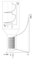
- FIG. 3 is an explanatory diagram showing an example of a temperature change of a solidification material during electron beam irradiation.
- FIG. 8 is an explanatory diagram showing a change in energy density of the solidification material shown in FIG.
- FIG. 3 is an explanatory diagram showing an example of a temperature change of a solidification material during electron beam irradiation.
- FIG. 10 is an explanatory diagram showing a change in energy density of the solidification material shown in FIG. 9;
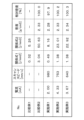
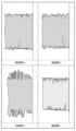
- FIG. 3 is a flowchart showing the main steps of repair processing for semiconductor manufacturing equipment components according to the embodiment. It is a table showing the relationship between various parameters related to layered manufacturing processing and the density of a shaped object. It is an explanatory view showing an outline of a molded object. This is a graph plotted by varying the electron beam current and scanning speed.
- FIG. 2 is an explanatory diagram showing a polycrystalline structure in a cross section of a component for semiconductor manufacturing equipment.
- FIG. 2 is an explanatory diagram showing a polycrystalline structure in a cross section of a component for semiconductor manufacturing equipment.
- FIG. 2 is an explanatory diagram showing a single crystal structure in a cross section of a component for semiconductor manufacturing equipment.
- FIG. 2 is an explanatory diagram showing a single crystal structure in a cross section of a component for semiconductor manufacturing equipment.
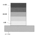
- FIG. 7 is a cross-sectional view showing a configuration example of a plasma processing system according to another embodiment. It is an explanatory view showing an example of composition of a shaped object constituted by slope modeling. It is an explanatory view showing an example of composition of a shaped object constituted by slope modeling. It is an explanatory view showing an example of composition of a shaped object constituted by slope modeling.
- a processing gas supplied into a chamber is excited to generate plasma to generate plasma on a semiconductor substrate (hereinafter simply referred to as "substrate") placed in the internal space of the chamber.
- substrate a semiconductor substrate placed in the internal space of the chamber.
- plasma treatments such as etching treatment, film formation treatment, and diffusion treatment are performed.
- a chamber internal member made of a high-purity silicon-containing material is arranged inside a plasma processing apparatus that performs plasma processing.
- this silicon-containing material is difficult to mold into a complicated shape without causing cracks or chips, and there are restrictions on the shape and dimensions of the chamber internal material to be molded.
- additive manufacturing used in the additive manufacturing method, additive manufacturing using conductive metal materials has been realized, but it is also expected to realize additive manufacturing using high-purity silicon-containing materials that make up the chamber internal materials mentioned above. There is. Expected high purity is 99% or higher purity, for example 99.99%, 99.999% and 99.9999% purity. If even higher purity is required, for example, the purity is 99.999999999%.
- the technology according to the present disclosure has been made in view of the above circumstances, and uses an additive manufacturing method to appropriately shape parts for semiconductor manufacturing equipment made of a high-purity silicon-containing material.
- a plasma processing system to which an additive manufacturing method according to an embodiment and a semiconductor manufacturing device component molded by the additive manufacturing method is applied will be described with reference to the drawings. Note that in this specification and the drawings, elements having substantially the same functional configuration are designated by the same reference numerals and redundant explanation will be omitted.
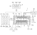
- FIG. 1 is a diagram for explaining a configuration example of a plasma processing system.
- a plasma processing system includes a plasma processing apparatus 1 and a controller 2.
- the plasma processing system includes, as an example, a capacitively coupled plasma processing apparatus 1.
- the capacitively coupled plasma processing apparatus 1 includes a plasma processing chamber 10, a gas supply section 20, a power supply 30, and an exhaust system 40. Further, the plasma processing apparatus 1 includes a substrate support section 11 and a gas introduction section. Substrate support 11 is arranged within plasma processing chamber 10 . The gas inlet is configured to introduce at least one processing gas into the plasma processing chamber 10 . The gas introduction section includes a shower head 13. The shower head 13 is arranged above the substrate support section 11 . In one embodiment, showerhead 13 forms at least a portion of the ceiling of plasma processing chamber 10 . Inside the plasma processing chamber 10, a plasma processing space 10s defined by the shower head 13, the side wall 10a of the plasma processing chamber 10, and the substrate support 11 is formed.
- the plasma processing chamber 10 has at least one gas supply port for supplying at least one processing gas to the plasma processing space 10s, and at least one gas exhaust port for discharging gas from the plasma processing space 10s.
- Plasma processing chamber 10 is grounded.
- showerhead 13 and substrate support 11 are electrically insulated from plasma processing chamber 10 .
- the substrate support section 11 includes a main body section 111 and a ring assembly 112.
- the upper surface of the main body 111 has a central region 111a for supporting the substrate W and an annular region 111b for supporting the ring assembly 112.
- a wafer is an example of a substrate W.
- the annular region 111b surrounds the central region 111a in plan view.
- the substrate W is arranged on the central region 111a, and the ring assembly 112 is arranged on the annular region 111b so as to surround the substrate W on the central region 111a. Therefore, the central region 111a is also called a substrate support surface for supporting the substrate W, and the annular region 111b is also called a ring support surface for supporting the ring assembly 112.
- the main body 111 includes a base 1110 and an electrostatic chuck 1111.
- base 1110 is constructed from a silicon-containing material such as silicon (Si) or silicon carbide (SiC).
- Base 1110 can function as a lower electrode.
- Electrostatic chuck 1111 is placed on base 1110.
- Electrostatic chuck 1111 includes a ceramic member 1111a and an electrostatic electrode 1111b disposed within ceramic member 1111a.
- Ceramic member 1111a has a central region 111a.
- ceramic member 1111a also has an annular region 111b. Note that another member surrounding the electrostatic chuck 1111, such as an annular electrostatic chuck or an annular insulating member, may have the annular region 111b.
- ring assembly 112 may be placed on the annular electrostatic chuck or the annular insulation member, or may be placed on both the electrostatic chuck 1111 and the annular insulation member.
- An RF/DC electrode is also referred to as a bias electrode if a bias RF signal and/or a DC signal, as described below, is supplied to at least one RF/DC electrode.
- the conductive member of the base 1110 and at least one RF or DC electrode may function as a plurality of lower electrodes.
- the electrostatic electrode 1111b may function as a lower electrode. Therefore, the substrate support 11 includes at least one lower electrode.
- the base 1110 (lower electrode) may be a component for semiconductor manufacturing equipment molded by the additive manufacturing method according to the embodiment.
- Ring assembly 112 includes one or more annular members.
- the one or more annular members include one or more edge rings and at least one cover ring.
- the edge ring is made of a conductive or insulating material
- the cover ring is made of an insulating material.
- the ring assembly 112 may be a component for semiconductor manufacturing equipment molded by the additive manufacturing method according to the embodiment.
- the substrate support section 11 may include a temperature control module configured to adjust at least one of the electrostatic chuck 1111, the ring assembly 112, and the substrate W to a target temperature.
- the temperature control module may include a heater, a heat transfer medium, a flow path 1110a, or a combination thereof.
- a heat transfer fluid such as brine or gas flows through the flow path 1110a.
- a channel 1110a is formed within the base 1110 and one or more heaters are disposed within the ceramic member 1111a of the electrostatic chuck 1111.
- the substrate support section 11 may include a heat transfer gas supply section configured to supply heat transfer gas to the gap between the back surface of the substrate W and the central region 111a.
- the shower head 13 is configured to introduce at least one processing gas from the gas supply section 20 into the plasma processing space 10s.
- the shower head 13 has at least one gas supply port 13a, at least one gas diffusion chamber 13b, and a plurality of gas introduction ports 13c.
- the processing gas supplied to the gas supply port 13a passes through the gas diffusion chamber 13b and is introduced into the plasma processing space 10s from the plurality of gas introduction ports 13c.
- the showerhead 13 also includes at least one upper electrode.
- the gas introduction section may include one or more side gas injectors (SGI) attached to one or more openings formed in the side wall 10a.
- the showerhead 13 (upper electrode) is constructed from a silicon-containing material such as silicon (Si) or silicon carbide (SiC). That is, the upper electrode may be a component for semiconductor manufacturing equipment that is molded by the additive manufacturing method according to the embodiment.
- the gas supply section 20 may include at least one gas source 21 and at least one flow rate controller 22.
- the gas supply 20 is configured to supply at least one process gas from a respective gas source 21 to the showerhead 13 via a respective flow controller 22 .
- Each flow controller 22 may include, for example, a mass flow controller or a pressure-controlled flow controller.
- gas supply 20 may include one or more flow modulation devices that modulate or pulse the flow rate of at least one process gas.
- Power supply 30 includes an RF power supply 31 coupled to plasma processing chamber 10 via at least one impedance matching circuit.
- RF power source 31 is configured to supply at least one RF signal (RF power) to at least one bottom electrode and/or at least one top electrode. Thereby, plasma is formed from at least one processing gas supplied to the plasma processing space 10s.
- RF power source 31 may therefore function as at least part of a plasma generation unit configured to generate a plasma from one or more process gases in plasma processing chamber 10 . Further, by supplying a bias RF signal to at least one lower electrode, a bias potential is generated in the substrate W, and ion components in the formed plasma can be drawn into the substrate W.
- the RF power supply 31 includes a first RF generation section 31a and a second RF generation section 31b.
- the first RF generation section 31a is coupled to at least one lower electrode and/or at least one upper electrode via at least one impedance matching circuit, and generates a source RF signal (source RF power) for plasma generation. It is configured as follows.
- the source RF signal has a frequency within the range of 10 MHz to 150 MHz.
- the first RF generator 31a may be configured to generate multiple source RF signals having different frequencies. The generated one or more source RF signals are provided to at least one bottom electrode and/or at least one top electrode.
- the second RF generating section 31b is coupled to at least one lower electrode via at least one impedance matching circuit, and is configured to generate a bias RF signal (bias RF power).
- the frequency of the bias RF signal may be the same or different than the frequency of the source RF signal.
- the bias RF signal has a lower frequency than the frequency of the source RF signal.
- the bias RF signal has a frequency within the range of 100kHz to 60MHz.
- the second RF generator 31b may be configured to generate multiple bias RF signals having different frequencies.
- the generated one or more bias RF signals are provided to at least one bottom electrode. Also, in various embodiments, at least one of the source RF signal and the bias RF signal may be pulsed.
- Power source 30 may also include a DC power source 32 coupled to plasma processing chamber 10 .
- the DC power supply 32 includes a first DC generation section 32a and a second DC generation section 32b.
- the first DC generator 32a is connected to at least one lower electrode and configured to generate a first DC signal.
- the generated first bias DC signal is applied to the at least one bottom electrode.
- the second DC generator 32b is connected to the at least one upper electrode and configured to generate a second DC signal.
- the generated second DC signal is applied to the at least one top electrode.
- At least one of the first and second DC signals may be pulsed.
- a sequence of voltage pulses is applied to at least one lower electrode and/or at least one upper electrode.
- the voltage pulse may have a pulse waveform that is rectangular, trapezoidal, triangular, or a combination thereof.
- a waveform generator for generating a sequence of voltage pulses from a DC signal is connected between the first DC generator 32a and the at least one bottom electrode. Therefore, the first DC generation section 32a and the waveform generation section constitute a voltage pulse generation section.
- the voltage pulse generation section is connected to at least one upper electrode.
- the voltage pulse may have positive polarity or negative polarity.
- the sequence of voltage pulses may include one or more positive voltage pulses and one or more negative voltage pulses within one period.
- the first and second DC generation units 32a and 32b may be provided in addition to the RF power source 31, or the first DC generation unit 32a may be provided in place of the second RF generation unit 31b. good.
- the exhaust system 40 may be connected to a gas exhaust port 10e provided at the bottom of the plasma processing chamber 10, for example.
- Evacuation system 40 may include a pressure regulating valve and a vacuum pump.
- the pressure regulating valve regulates the internal pressure of the plasma processing space 10s.
- the vacuum pump may include a turbomolecular pump, a dry pump, or a combination thereof.
- the control unit 2 processes computer-executable instructions that cause the plasma processing apparatus 1 to perform various steps described in this disclosure.
- the control unit 2 may be configured to control each element of the plasma processing apparatus 1 to perform the various steps described herein. In one embodiment, part or all of the control unit 2 may be included in the plasma processing apparatus 1.
- the control unit 2 may include a processing unit 2a1, a storage unit 2a2, and a communication interface 2a3.
- the control unit 2 is realized by, for example, a computer 2a.
- the processing unit two a1 may be configured to read a program from the storage unit two a2 and perform various control operations by executing the read program. This program may be stored in the storage unit 2a2 in advance, or may be acquired via a medium when necessary.
- the acquired program is stored in the storage unit 2a2, and is read out from the storage unit 2a2 and executed by the processing unit 2a1.
- the medium may be various storage media readable by the computer 2a, or may be a communication line connected to the communication interface 2a3.
- the processing unit 2a1 may be a CPU (Central Processing Unit).
- the storage unit 2a2 may include a RAM (Random Access Memory), a ROM (Read Only Memory), an HDD (Hard Disk Drive), an SSD (Solid State Drive), or a combination thereof. Good.
- the communication interface 2a3 may communicate with the plasma processing apparatus 1 via a communication line such as a LAN (Local Area Network).
- the plasma formed in the plasma processing apparatus 1 is a capacitively coupled plasma (CCP), but the plasma formed in the plasma processing space is an inductive plasma.
- ICP Inductively coupled plasma
- ECR plasma Electro-Cyclotron-resonance plasma
- HWP helicon wave excited plasma
- SWP Surface Wave Plasma
- various types of plasma generation units may be used, including an AC (Alternating Current) plasma generation unit and a DC (Direct Current) plasma generation unit.
- the AC signal (AC power) used in the AC plasma generator has a frequency in the range of 100 kHz to 10 GHz. Therefore, the AC signal includes an RF (Radio Frequency) signal and a microwave signal.
- the RF signal has a frequency within the range of 100kHz to 150MHz.
- FIG. 2 is an explanatory diagram schematically showing the configuration of a layered manufacturing apparatus 200 according to an embodiment.
- the additive manufacturing apparatus 200 includes a chamber 210, a powder storage section 220, an electron beam (EB) irradiation system (hereinafter referred to as an EB irradiation system) 230, and a recoater 240.
- EB electron beam
- the modeling plate 211 is made of the same material as the coagulation material (in this embodiment, silicon (Si: 4.3 ppm (room temperature)), or a material with a linear expansion coefficient similar to that of the coagulation material (for example, titanium (Ti: 8.8 ppm (room temperature)). )) may be composed of a material having a linear expansion coefficient of: Note that the modeling plate 211 is configured such that its temperature can be controlled by a temperature controller (not shown).
- the temperature control unit may be a heater, a heat transfer medium, a flow path, the EB irradiation system 230 described below, or a combination thereof.
- a temperature sensor (not shown) for measuring the temperature of the modeling plate 211 may be connected to the modeling plate 211.
- a lifting platform 212 is provided at the bottom of the modeling plate 211, which allows the height position of the modeling plate 211 to be adjusted.
- Silicon powder from a powder storage section 220 which will be described later, is configured to be able to be supplied toward the upper surface of the modeling plate 211, and the modeling plate 211 can be adjusted to the silicon powder supply position and to the modeling plate by the raising and lowering movement of the elevating table 212. It is configured to be movable between the molding position and the position where the electron beam is irradiated.
- the powder storage section 220 contains a material that is a raw material for parts for semiconductor manufacturing equipment molded by the additive manufacturing method according to the embodiment, and contains a molding electron beam (hereinafter simply referred to as " In this embodiment, pure silicon powder (Si) with a purity of 99% or more is stored, which is melted and solidified by irradiation with an electron beam (sometimes referred to as an electron beam). Purity of 99% or more means, for example, purity of 99.99%, 99.999%, and 99.9999%. If even higher purity is required, for example, the purity is 99.999999999%.
- the average powder particle size (D50) of the silicon powder as the solidifying material is desirably 25 ⁇ m or more and 300 ⁇ m or less, more preferably 80 ⁇ m or more and 150 ⁇ m or less.
- the average powder particle size (D50) of silicon powder is measured by existing particle size analysis - laser diffraction/scattering method (JIS Z8825), and is determined when the cumulative particle size is 50% in the particle size distribution converted based on volume. particle size may be employed.
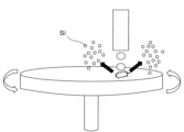
- the silicon powder used as the coagulation material may be manufactured by disk atomization, which is a conventional powder manufacturing method. Specifically, in the production of silicon powder by disk atomization, as shown in Figure 3, molten silicon is dropped onto a disk rotating at high speed, and the rotational force of the disk scatters the molten silicon as fine droplets to form silicon powder. Manufacture. By manufacturing silicon powder using this disk atomization, it is possible to manufacture powder with a shape closer to a perfect sphere, compared to other powder manufacturing methods such as gas atomization. Furthermore, unlike gas atomization, gas is not used during powder production, so gas entrainment during powder production is suppressed, and defects such as gas components being mixed into the produced silicon powder are less likely. Further, according to this manufacturing method, silicon powder is generated only by dropping molten silicon onto a rotating disk, so silicon powder can be manufactured at a relatively low cost.
- the silicon powder stored in the powder storage section 220 is supplied within the chamber 210 onto the modeling plate 211 placed at the silicon powder supply position.
- the solidifying material stored in the powder storage section 220 is not limited to the pure silicon (Si) described above, but may also be a composite of pure silicon (Si) and another type of powder.
- the material may be powder.
- examples of the material (composite material) to be integrated with pure silicon (Si) include carbon (C), silicon carbide (SiC), alumina (Al 2 O 3 ), aluminum nitride (AlN), or yttrium oxide ( Examples include non-metallic materials such as Y 2 O 3 ) and metallic materials such as aluminum (Al).
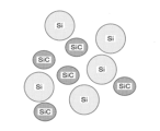
- the above-mentioned composite material powder as a coagulation material has an overall average powder particle size (D50) of 25 ⁇ m or more and 300 ⁇ m or less, and has a particle size larger than or equal to the average powder particle size of the powder to be composited with pure silicon.
- the particle size (see FIG. 4) is desirable.
- the powder that is composited with pure silicon silicon carbide (SiC) in the illustrated example) does not need to be completely covered with pure silicon, but it is desirable that it is bonded to the extent that it does not separate during flow. .
- the average powder particle size (D50) of composite material powder and powder composite with pure silicon is measured by existing particle size analysis - laser diffraction/scattering method (JIS Z8825), as an example, and the particle size distribution is calculated based on volume.
- the particle size at which the accumulation is 50% can be adopted.
- each of the plurality of powder storage parts 220 may be arranged in the additive manufacturing apparatus 200.
- each of the plurality of powder storage parts 220 contains another type of coagulation to be mixed with the pure silicon powder (Si) and composite material powder. Powders of materials for use may be stored.
- examples of mixing materials to be mixed with pure silicon powder (Si) and composite material powder include carbon (C), silicon carbide (SiC), alumina (Al 2 O 3 ), aluminum nitride (AlN), At least one of the mixing materials selected from nonmetallic materials such as yttrium oxide (Y 2 O 3 ) or ceramics, metallic materials such as aluminum (Al), or composite materials such as MMC (Metal Matrix Composites) is used. Can be stored. Note that in the embodiment, "mixing" of powders is different from the state in which multiple powders are combined (integrated) shown in FIG. This refers to the state in which the materials are mixed together (in a state that can be sieved).
- additive manufacturing in addition to or instead of additive manufacturing using pure silicon powder (Si) alone, pure silicon powder (Si) and the nonmetallic material, the metallic material, or the composite material are used. Additive manufacturing with mixed powders may also be performed.
- the EB irradiation system 230 includes an electron gun 231 as an irradiation unit disposed above the modeling plate 211 inside the chamber 210, and a head 232 that serves as an irradiation source for the modeling electron beam irradiated from the electron gun 231.
- the electron beam for modeling irradiated from the electron gun 231 is configured to be able to be irradiated onto any position on the modeling plate 211 via, for example, a focusing mirror (not shown) or a polarizing mirror (not shown). Further, the beam diameter of the modeling electron beam irradiated from the electron gun 231 is configured to be arbitrarily changeable.
- the modeling energy beam irradiated onto the silicon powder on the modeling plate 211 is not limited to an electron beam, and may be, for example, a laser beam (SL: Selective Laser).
- the additive manufacturing apparatus 200 may include a laser beam irradiation system (not shown) instead of the EB irradiation system 230.
- the recoater 240 is disposed inside the chamber 210 at least above the modeling plate 211.
- the recoater 240 is configured to be movable in the horizontal direction, and performs an operation of spreading silicon powder from the powder storage section 220 onto the upper surface of the modeling plate 211 (so-called recoating).
- the evacuation system may include a pressure regulating valve and a vacuum pump.
- a pressure regulating valve regulates the internal pressure of chamber 210.
- the vacuum pump may include a turbomolecular pump, a dry pump, or a combination thereof.
- a powder recovery system (not shown) may be connected to the chamber 210.
- the powder recovery system may be connected to the exhaust system in one example.
- the powder recovery system collects the solidifying material that was supplied onto the modeling plate 211 and was not used in the layered manufacturing process described below, in other words, the solidifying material that was not irradiated with the modeling electron beam from the EB irradiation system 230. By collecting the solidifying material and supplying it onto the modeling plate 211 again, the collected solidifying material can be reused.
- control unit 250 processes computer-executable instructions that cause the additive manufacturing apparatus 200 to perform steps related to various additive manufacturing processes described in this disclosure.
- Control unit 250 may be configured to control each element of additive manufacturing apparatus 200 to perform the various steps described herein. In one embodiment, part or all of the control unit 250 may be included in the additive manufacturing apparatus 200.
- the control unit 250 may include a processing unit 250a1, a storage unit 250a2, and a communication interface 250a3.
- the control unit 250 is realized by, for example, a computer 250a.
- the processing unit 250a1 may be configured to read a program from the storage unit 250a2 and perform various control operations by executing the read program.
- This program may be stored in advance in the storage unit 250a2, or may be acquired via a medium when necessary.
- the acquired program is stored in the storage unit 250a2, and is read out from the storage unit 250a2 and executed by the processing unit 250a1.
- the medium may be a variety of storage media readable by computer 250a, or may be a communication line connected to communication interface 250a3.
- the processing unit 250a1 may be a CPU (Central Processing Unit).
- the storage unit 250a2 includes a RAM (Random Access Memory), a ROM (Read Only Memory), an HDD (Hard Disk Drive), an SSD (Solid State Drive), or a combination thereof. You can.
- the communication interface 250a3 may communicate with the plasma processing apparatus 1 via a communication line such as a LAN (Local Area Network).
- FIG. 6 is a flow diagram showing an example of the main steps of the additive manufacturing process performed using the additive manufacturing apparatus 200 configured as described above.
- pure silicon powder with a purity of 99% or more is used as the solidification material, and the case where parts for semiconductor manufacturing equipment are molded by electron beam additive manufacturing processing will be explained as an example. conduct.
- step S St0-1 to Step St0-2 in FIG. 6 advance preparations for the additive manufacturing are first performed.
- step S St0-1 to Step St0-2 in FIG. 6 advance preparations for the additive manufacturing are first performed.
- step S St0-3 to Step St0 in FIG. 6 the equipment-related preparations related to additive manufacturing.
- CAD data (3D data) of a semiconductor manufacturing equipment component to be manufactured is converted into slice data (step St0-1).
- components for semiconductor manufacturing equipment are manufactured by repeating the supply of solidification material to the modeling plate 211 (lamination) and the cooling (solidification) of the supplied solidification material.
- the completed form data (3D CAD data) of the semiconductor manufacturing equipment component to be manufactured is decomposed into unit data (slice data) for each layer in the stacking direction of the solidification material.
- the supply conditions of the solidifying material (supply position and supply amount (supply thickness)) and the irradiation conditions of the electron beam for modeling are applied to each slice data (step St0-2) and determined.
- Irradiation of the modeling electron beam from the EB irradiation system 230 is controlled based on the irradiation conditions determined.
- the CAD data of the semiconductor manufacturing device components used in the layered manufacturing process may be stored in the storage unit 250a2 in advance, or may be acquired via a storage medium when necessary.
- a modeling plate 211 serving as a modeling base material is placed at a predetermined position within the chamber 210 (step St0-3).
- a ground wire for avoiding charge accumulation and a temperature sensor for temperature control are connected to the lower part of the plate.
- a heat insulating layer is then formed around the modeling plate 211 (step St0-4). Specifically, as shown in FIG. 2, the lower part of the modeling plate 211 placed in the chamber 210 is filled with pure silicon powder, which is a material for solidification.
- step St1 the inside of the chamber 210 is evacuated by an exhaust system (not shown) (step St1 in FIG. 6).
- step St1 it is desirable to evacuate the inside of the chamber 210 to a high vacuum, preferably to 1.0 ⁇ 10 ⁇ 4 Torr or less.
- the semiconductor manufacturing apparatus is molded by the additive manufacturing process according to the embodiment.
- the amount of impurities (for example, air, etc.) mixed into the parts increases.
- the amount of impurities in the chamber 210 can be reduced by evacuating the inside of the chamber 210 to 1.0 ⁇ 10 ⁇ 4 Torr or less, and as a result, the amount of impurities in the chamber 210 can be reduced.
- an inert gas for example, helium (He) gas
- a gas supply unit not shown to adjust the atmosphere inside the chamber 210 (see FIG. 6).
- step St3 the modeling plate 211 is heated (preheated) before supplying the silicon powder (step St3 in FIG. 6).
- step St3 the temperature of the modeling plate 211 is raised to 800° C. or higher and lower than the melting point of the solidification material (silicon powder) to be supplied in a later step.
- the temperature of the modeling plate 211 is maintained at a preheating temperature (a temperature of 800° C. or higher and lower than the melting point of silicon powder) until the molding of the semiconductor manufacturing equipment component is completed. do.
- a preheating temperature a temperature of 800° C. or higher and lower than the melting point of silicon powder
- step St6 If the temperature of the modeling plate 211 becomes less than 800° C., as will be described later, there is a risk that silicon powder will be scattered in the subsequent electron beam irradiation step (step St6, described below), and it may be necessary to stop the additive manufacturing process. be. On the other hand, if the preheating temperature of the modeling plate 211 is higher than the melting point of the silicon powder, the silicon powder will melt near the top surface of the modeling plate 211, and as a result, there is a risk that the modeling plate 211 will be misaligned.
- the silicon powder since the silicon powder is melted and has viscosity, the silicon powder may adhere to the recoater 240 during the above-mentioned recoating, and as a result, the modeling plate 211 and the recoater 240 may become stuck together.
- the method of heating the modeling plate 211 is not particularly limited.
- heating may be performed using a heating mechanism (not shown) disposed inside or outside the modeling plate 211.
- a modeling electron beam may be irradiated toward the modeling plate 211 from the EB irradiation system 230 disposed above the modeling plate 211, and heating may be performed by the energy of the irradiated modeling electron beam.
- the silicon powder stored in the powder storage section 220 is then supplied onto the modeling plate 211 and deposited (step St4 in FIG. 6). At this time, the modeling plate 211 is placed at the silicon powder supply position by the lifting table 212.
- step St4 in order to melt the silicon powder layer (hereinafter sometimes referred to as "deposited powder") appropriately deposited on the modeling plate 211 in the subsequent electron beam irradiation step (step St6 described below), It is desirable that the amount of deposited silicon powder (supplied amount) be controlled so that the thickness (layer thickness) of the silicon powder deposited on the modeling plate 211 is close to the particle size of the silicon powder. .
- the thickness of the silicon powder deposited on the modeling plate 211 is preferably 80 ⁇ m or more. However, the thickness of the silicon powder is not limited to 80 ⁇ m or more.
- silicon powder having an average powder particle size (D50) of 25 ⁇ m or more and 300 ⁇ m or less, more preferably 80 ⁇ m or more and 150 ⁇ m or less is selected.
- D50 average powder particle size
- the average particle size of the silicon powder is less than 25 ⁇ m, there is a risk that the silicon powder will scatter in the subsequent electron beam irradiation step (Step St6 described below), making it necessary to stop the additive manufacturing process, or damaging the semiconductor manufacturing equipment to be molded. There is a risk that the density of the parts for use will decrease.
- the average particle size of the silicon powder exceeds 300 ⁇ m, although the semiconductor manufacturing equipment parts can be molded, the molding accuracy (resolution) of the semiconductor manufacturing equipment parts decreases, and the semiconductor manufacturing equipment parts are formed in the desired shape. There is a possibility that it will not be possible to mold the product.
- step St6 when the average particle size of the silicon powder is 80 ⁇ m or more and 150 ⁇ m or less, scattering of the silicon powder in the subsequent electron beam irradiation process (step St6 described below) can be suitably suppressed, and the desired shape and density can be maintained in the semiconductor manufacturing device. Can mold parts for use.
- step St6 a single layer of silicon powder deposited on the modeling plate 211 is irradiated with the modeling electron beam in multiple stages (multiple times) as described later. By doing this, we aim to suppress the scattering of the silicon powder.
- parts for semiconductor manufacturing equipment can be formed by (one time) irradiation with a shaping electron beam.
- the silicon powder as the deposited powder is heated (preheated) (step St5 in FIG. 6).
- the silicon powder is heated by heat transfer from the preheated modeling plate 211, by the heating mechanism (not shown) for heating the modeling plate 211, or by the modeling electron beam from the EB irradiation system 230.
- the temperature is raised to a desired preheating temperature (800° C. or higher) by irradiation.
- step St6 the temperature of the silicon powder becomes less than 800 degrees Celsius, as mentioned above, there is a risk that the deposited silicon powder will scatter in the subsequent electron beam irradiation process (step St6 described below) and it will be necessary to stop the modeling.
- step St6 the subsequent electron beam irradiation process
- charges are accumulated in the silicon powder irradiated with the electron beam.
- Coulomb force is generated between the silicon powders in which charges are accumulated, which may cause the silicon powders to scatter.
- the deposited powder is preheated prior to the subsequent electron beam irradiation step (step St6 described below).
- step St6 the subsequent electron beam irradiation step
- the temperature of the silicon powder is increased in stages, especially in the initial stage of preheating.
- the output of the modeling electron beam is increased in stages.
- the accumulation of charge is suppressed, especially in the early stage of preheating when the silicon powders have not yet bonded together, and it is possible to more appropriately bond the silicon powders together. It is possible to promote binding and suppress scattering of silicon powder.
- step St6 an electron beam is then irradiated from the EB irradiation system 230 toward the silicon powder on the modeling plate 211 (step St6 in FIG. 6).
- the modeling plate 211 is placed at the modeling position by the lifting table 212.
- the irradiation position of the electron beam from the electron gun 231 is scanned on the modeling plate 211.
- step St6 the silicon powder on the modeling plate 211 is irradiated with an electron beam to partially melt the silicon powder at the irradiation position of the electron beam, thereby binding the silicon powder to each other.
- the layer of silicon powder formed on the modeling plate 211 by binding of the silicon powder may be referred to as a "molten silicon layer (molten layer)".
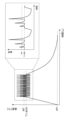
- the silicon powder on the modeling plate 211 is irradiated with the electron beam in multiple stages (three stages in the example of FIG. 7).
- the temporal irradiation interval between each stage of the multi-stage electron beam irradiation is such that the silicon powder heated by the previous electron beam irradiation is cooled down to the preheating temperature (800°C or higher) before electron beam irradiation.
- the irradiation interval is controlled such that the next electron beam is irradiated after the first electron beam has been irradiated.
- the energy density of the electron beam irradiated in multiple stages is controlled so that the temperature of the outermost surface of the object (silicon powder that is the target of electron beam irradiation) rises in stages. .
- the electron beam irradiation is controlled such that the energy density of the electron beam irradiated in the later stage is higher than the energy density of the electron beam irradiated in the previous stage.
- the temperature of the silicon powder to be irradiated with the electron beam is less than 800° C., there is a risk that the silicon powder will scatter during the irradiation with the electron beam.
- silicon powder is heated by single electron beam irradiation as shown in FIGS. 9 and 10, for example, the temperature of one silicon powder is raised all at once by one electron beam irradiation.
- the electron beam is applied to one silicon powder in multiple stages (multiple times) so that the temperature of the silicon powder increases in stages. irradiate.
- the silicon powder that is the target of electron beam irradiation is melted and bonded in stages. Then, the silicon powder thus melted and bonded is irradiated with an electron beam (the last step of the electron beams irradiated in multiple steps) to form a molten silicon layer (molten layer).
- an electron beam (electron beams other than the last stage among the electron beams irradiated in multiple stages) is used to melt and bond the silicon powder in stages, and a molten silicon layer is formed from the silicon powder.
- the electron beam for the final formation (the last stage of electron beams among the electron beams irradiated in multiple stages) is continuously irradiated.
- the weight per particle of powder increases. This suppresses scattering of the solidifying material due to electron beam irradiation.
- the molten silicon layer may be formed by single-shot (one time) electron beam irradiation as shown.
- Relational expression (1) ([voltage] x [current]) / ([beam diameter] x [scan speed])
- Relational expression (2) ([voltage] x [current]) / ([beam diameter] x [scan speed] x [thickness of one powder layer])
- the units of various parameters are as follows. Voltage [kV] Current [mA] Beam diameter (diameter) [mm] Scan speed [mm/sec] Thickness of one layer of powder (deposited powder) [mm]
- relational expression (1) preferably satisfies 0.3 or more and 3.0 or less, more preferably 0.5 or more and 3.0 or less.
- relational expression (2) desirably satisfies 5.3 or more and 50.0 or less, more preferably 8.4 or more and 50.0 or less.
- the relational expression (1) exceeds 3.0, or if the relational expression (2) exceeds 50.0, the energy of the electron beam irradiated from the electron gun 231 becomes excessive, which causes excessive silicon powder There is a possibility that the shape of the semiconductor manufacturing equipment component to be melted and molded cannot be properly controlled.
- the relational expression (1) is less than 0.3, or if the relational expression (2) is less than 5.3, the energy of the electron beam irradiated from the electron gun 231 does not reach the required amount.
- the modeled object semiconductor manufacturing device component
- the shaped object (semiconductor manufacturing equipment component) can be molded into the desired shape, and The density of molded parts for semiconductor manufacturing equipment can be increased.
- the above relational expression (1) satisfies 0.3 or more and 3.0 or less, more preferably 0.5 or more and 3.0 or less, or the above relational expression (2) is preferably 5.3 or more and 50.0 or less, more preferably 8.4 or more and 50.0 or less.
- the above relational expression (1) or the above relational expression (2) is the irradiation condition when the solidification material (pure silicon powder) is irradiated with the electron beam in a single shot, or when the electron beam is irradiated in multiple stages. This can be applied to at least the final stage electron beam irradiation conditions.
- step St7 the molten silicon layer is solidified by cooling.
- the solidified molten silicon layer may be referred to as a "solidified silicon layer (solidified layer)".
- the molten silicon layer be cooled in a short time, that is, that the molten silicon layer be rapidly solidified.
- the cooling (solidification) time of the molten silicon layer is preferably 1 second or less. desirable.
- the method for cooling the molten silicon layer is not particularly limited, and may be cooled by natural heat radiation within the chamber 210, for example.
- Step St4 a series of process cycles including the above deposition of silicon powder (Step St4), melting of the silicon powder (Steps St5, Step St6), and solidification of the molten silicon layer (Step St7) is shown in FIG.
- the process is repeated until the desired shape of the semiconductor manufacturing equipment component is obtained.
- step St4 from the second cycle onwards in addition to the modeling plate 211, a solidification material is applied on the solidification silicon layer (base material layer) molded in the previous cycle. Supply pure silicon powder.
- another solidified silicon layer is laminated and formed on one solidified silicon layer.
- steps St4 to Step St7 it is determined whether a further cycle of the additive manufacturing process (steps St4 to Step St7) is necessary, and if it is determined that it is necessary (the molding of parts for semiconductor manufacturing equipment is If the process is not completed), as shown in FIG. 6, the process returns to step St4 and the process from step St4 to step St7 is repeated. Further, if it is determined that a further process cycle of the layered manufacturing process is unnecessary (if a component for a semiconductor manufacturing device having a desired shape is obtained), the layered manufacturing process is ended.
- the temperature of the inside of the chamber 210 containing the molded semiconductor manufacturing device parts and the modeling plate 211 is lowered, and further heat-treated as necessary (steps St8 and St9 in FIG. 6). . Thereafter, the molded semiconductor manufacturing equipment component is taken out from inside the chamber 210. The semiconductor manufacturing device components taken out from the chamber 210 may then be processed, formed, or repaired as necessary (step St10 in FIG. 6).
- step St4 to step St7 the process cycle of the additive manufacturing process (step St4 to step St7) is repeatedly executed, but the repetition may be omitted depending on the intended use of the semiconductor manufacturing equipment component to be molded. . That is, the additive manufacturing process may be performed only once.
- FIG. 11 is a flowchart illustrating an example of the main steps of a process for forming (repairing) a component for a semiconductor manufacturing device (hereinafter simply referred to as a repair process).
- the repair process is performed, for example, on semiconductor manufacturing equipment components containing silicon that have been consumed by plasma processing in the plasma processing apparatus 1 shown in FIG.
- the parts for semiconductor manufacturing equipment containing silicon that are consumed by plasma processing are the base 1110, the ring assembly 112, and/or the shower head 13.
- repair processing is performed not only on parts for semiconductor manufacturing equipment that are worn out due to plasma processing, but also on parts for semiconductor manufacturing equipment that are missing and/or damaged due to various factors.
- 3D data of the semiconductor manufacturing equipment component to be repaired is obtained using a 3D scanner (step St10-1 in FIG. 11).
- the 3D data includes data such as the amount of wear, the position of wear (area of wear), and the shape of wear.
- the acquired 3D data is output to a 3D scanner control device (not shown).
- step St10-1 the 3D data acquired in step St10-1 is compared with 3D data for molding the semiconductor manufacturing equipment component to be repaired (for example, the CAD data used in step St0-1 in FIG. 6).
- Step St10-2 in FIG. 11 More specifically, by comparing CAD data, which is 3D data of a completed semiconductor manufacturing equipment component, with the 3D data of the semiconductor manufacturing equipment component to be repaired obtained in step St10-1, both data are Get the difference value. If the obtained difference value (amount of consumption) exceeds a predetermined threshold, the portion where this difference value exceeds the threshold is treated as the portion of the semiconductor manufacturing equipment component to be repaired that requires repair (hereinafter referred to as " (consumable parts).
- step St10-3 in FIG. 11 repair of the semiconductor manufacturing equipment component (step St10-3 in FIG. 11) is then started.
- a method for repairing a component for a semiconductor manufacturing device is, for example, the same as the layered manufacturing process shown in FIG. 6, and is performed using the layered manufacturing apparatus 200 described above, for example. That is, the consumable part identified in step St10-2 is regarded as the part to be processed in the additive manufacturing process, and silicon powder is supplied to the consumable part, deposited, heated (preheated), and irradiated with an electron beam to the silicon powder. , and cooling of the molten silicon powder.
- the temperature of the semiconductor manufacturing equipment component is adjusted to at least the preheating temperature (800° C. or higher and silicon powder instead of the modeling plate 211) until the repair of the semiconductor manufacturing equipment component is completed. It is preferable to maintain the temperature at a temperature lower than the melting point of Moreover, instead of the modeling plate 211, it is preferable that at least the components for the semiconductor manufacturing device be made of the same material as the solidification material or a material having a linear expansion coefficient close to that of the solidification material. In other words, the same material as the material constituting the semiconductor manufacturing equipment component, or a material with a linear expansion coefficient close to that, is selected as the material for solidification.
- the electron beam irradiation conditions are adjusted based on the above relational expression (1) or the above relational expression (2). It is desirable to adjust the In addition, other conditions related to the repair process, such as the conditions of the silicon powder to be deposited on the semiconductor manufacturing equipment parts to be repaired (type, particle size, mixing ratio, etc.), the internal pressure of the chamber 210, the conditions of the semiconductor manufacturing equipment parts to be repaired, etc.
- the heating method and the like may be the same as the above-described layered manufacturing method.
- step St10-4 in FIG. 11 the temperature inside the chamber 210 containing the repaired semiconductor manufacturing equipment components and the modeling plate 211 is lowered (step St10-4 in FIG. 11), and further heat treatment is performed as necessary (step St10-4 in FIG. 11).
- step St10-5) is carried out.
- the repaired semiconductor manufacturing equipment component is taken out from inside the chamber 210 (step St10-6 in FIG. 11), and a series of semiconductor manufacturing equipment component repair processing is completed.
- step St10-2 if the difference value (amount of consumption) acquired in the above-mentioned 3D data comparison (step St10-2) does not exceed the predetermined threshold, as shown in FIG.
- the semiconductor manufacturing equipment component may be taken out of the chamber 210 (step St10-6) without repairing the component (steps St10-3 to St10-5).
- the above relational expression (1) is set to 0.3 or more and 3.0 or less, preferably 0.5 or more and 3.0 or less, or the above relational expression (2)
- the value is set to 5.3 or more and 50.0 or less, preferably 8.4 or more and 50.0 or less, even when pure silicon powder with a purity of 99% or more is used as a material for solidification, it is possible to properly form a semiconductor. Can mold and repair parts for manufacturing equipment.
- Figure 12 shows the density and relative density of semiconductor manufacturing equipment parts molded under the respective conditions when the values of the above relational expressions (1) and the above relational expressions (2) are adjusted by changing various parameters. It is a table showing density.
- density [g/cm 3 ] shown in FIG. 12 represents the measured density of a molded semiconductor manufacturing equipment component
- relative density [%] represents the density of silicon powder as a solidification material
- 100 '' represents the relative density of parts for semiconductor manufacturing equipment.
- relational expression (1) in comparative example 1, relational expression (1) is 0.3 or more, but when relational expression (2) is less than 5.3, in comparative example 2, relational expression (1) exceeds 3.0. However, the results are shown when relational expression (2) also exceeds 50.0.
- Example 1 in Example 1, if relational expression (1) is 0.3 or more and less than 0.5, and relational expression (2) is 5.3 or more and less than 8.4, then Example 2 and Example 3 are The results are shown when the equation (1) satisfies the conditions of 0.5 or more and 3.0 or less, and the relational expression (2) satisfies the conditions of 8.4 or more and 50.0 or less.
- the temperature of the modeling plate 211 was always maintained at 800° C. or higher.
- FIG. 13 is an explanatory diagram showing the outline of parts for semiconductor manufacturing equipment molded under the respective conditions shown in FIG. 12. Specifically, outlines of parts for semiconductor manufacturing equipment molded under the conditions of Comparative Example 2, Example 1, Example 2, and Example 3 are shown, respectively. Note that these outlines are images taken by X-ray CT scan.
- Comparative Example 1 shown in FIG. 12 the relational expression (2) is less than 5.3, and as described above, the energy of the electron beam irradiated from the electron gun 231 is weak, and the modeled object is damaged during the additive manufacturing process. It was peeled off from the modeling plate 211. That is, it was not possible to properly mold parts for semiconductor manufacturing equipment.
- the relative density of the molded semiconductor manufacturing equipment component is 100.0, that is, the relative density exceeds 99% without any impurities being mixed in from the silicon powder state as the solidification material.
- the relational expression (1) exceeds 3.0
- the relational expression (2) exceeds 50.0, and as described above, the energy of the electron beam irradiated from the electron gun 231 is strong, and as shown in FIG.
- the shape of the molded semiconductor manufacturing equipment component was greatly distorted (became flat). In other words, it was not possible to obtain a component for semiconductor manufacturing equipment having a desired shape.
- Example 1 of FIG. 12 as shown in FIG. 13, the shape of the semiconductor manufacturing equipment component did not collapse, that is, it was possible to obtain the semiconductor manufacturing equipment component of the desired shape.
- relational expression (1) is 0.3 or more and less than 0.5
- relational expression (2) is 5.3 or more and less than 8.4
- the density of the molded semiconductor manufacturing equipment component decreases ( relative density 97.9%).
- Example 2 and Example 3 in FIG. 12 the conditions of relational expression (1) of 0.5 or more and 3.0 or less and relational expression (2) of 8.4 or more and 50.0 or less were satisfied.
- the relative density of the molded semiconductor manufacturing equipment parts was 100.2 in Example 2 and 100.3 in Example 3, which means that A dense component for semiconductor manufacturing equipment with a relative density of over 99% could be molded without contamination with impurities.
- the shape of the semiconductor manufacturing equipment component did not collapse, that is, it was possible to obtain a semiconductor manufacturing equipment component with a desired shape.
- the present inventors found that when pure silicon powder (purity of 99% or more) is used as a coagulation material, the above relational expression (1) is 0.3 or more. It has been found that it is possible to mold a shaped article (a component for semiconductor manufacturing equipment) in a desired shape by satisfying the condition that . In particular, by satisfying the condition that the above relational expression (1) is 0.5 or more and 3.0 or less, or the above relational expression (2) is 8.4 or more and 50.0 or less, a desired shape and high density can be obtained. (relative density of 99% or more) (parts for semiconductor manufacturing equipment) can be molded.
- the present inventors have discovered that by adjusting the output current of the electron beam and the scanning speed of the electron beam, the crystallization of the formed object (parts for semiconductor manufacturing equipment) after printing is achieved.
- the structure crystalline structure of silicon
- the structure can be controlled. That is, by adjusting the current and scanning speed of the electron beam, it is possible to control the components for semiconductor manufacturing equipment to be monocrystalline silicon or polycrystalline silicon.
- the present inventors performed an additive manufacturing process under conditions in which the current and scan speed of the electron beam were varied as shown in FIG. 14, and observed the crystal structure of the molded parts for semiconductor manufacturing equipment.
- FIG. 14 under the conditions indicated by white circles ( ⁇ ), the crystal structure became a single crystal structure, and under the conditions indicated by black circles ( ⁇ ), the crystal structure became a polycrystal structure.
- FIG. 15 shows a polycrystalline structure in a cross section of a component for semiconductor manufacturing equipment
- FIG. 15A is a cross-sectional view in a direction parallel to the modeling direction
- FIG. 15B is a cross-sectional view in a direction perpendicular to the manufacturing direction.
- the shade of color in FIG. 15 indicates the orientation of the crystal orientation, and crystals with the same shade of color are crystals oriented in the same direction.
- This polycrystalline structure was obtained under one of the conditions indicated by the black circle ( ⁇ ) in FIG. 14, that is, the current was 4.00 mA and the scan speed was 2000 mm/s.
- FIGS. 15A and 15B a plurality of crystal grains with different orientations are formed in the cross section in any direction.
- semiconductor manufacturing equipment parts having a polycrystalline structure were similarly molded.
- FIG. 16 shows a single-crystalline structure in a cross section of a component for semiconductor manufacturing equipment
- FIG. 16A is a cross-sectional view in a direction parallel to the modeling direction
- FIG. 16B is a cross-sectional view in a direction perpendicular to the manufacturing direction.
- the color shading in FIG. 16 indicates the orientation of the crystal orientation, and crystals with the same color shading are crystals facing the same orientation.
- This single-crystal structure is obtained under one of the conditions indicated by the white circle ( ⁇ ) in FIG. 14, that is, when the current is 3.67 mA and the scan speed is 640 mm/s, and corresponds to Example 3 shown in FIG. 12. obtained under the conditions. As shown in FIG.
- a component for semiconductor manufacturing equipment having a single crystal structure is molded under the conditions that the electron beam current is 4.33 mA or less and the scan speed is 753 mm/s or less. can do.
- the upper limit values of the current and scan speed for obtaining a single crystal structure are as described above, but the lower limit values of the current and scan speed are such that the above relational expression (1) is 0.3 or more and 3.0 or less, Alternatively, the above relational expression (2) is a value that satisfies the condition of 5.3 or more and 50.0 or less. In such a case, as described above, it is possible to obtain a component for semiconductor manufacturing equipment having a desired shape.
- the silicon substrate can be formed in the desired shape. can be molded.
- the desired shape and high density relative It is possible to mold silicon substrates with a density of 99% or higher.
- the crystal structure of the silicon substrate after modeling can be controlled.
- a silicon substrate with a single crystal structure can be formed under the conditions that the electron beam current is 4.33 mA or less and the scan speed is 753 mm/s or less.
- the movement speed of electrons within the crystal is faster than that in a polycrystalline structure.
- the performance of the IC chip can be improved. I can do it.
- the silicon substrate is formed by performing a layered manufacturing process using an electron beam
- the silicon substrate can be manufactured at high speed and in a desired shape.
- the crystal structure of the silicon substrate can be controlled to a single crystal structure.
- additive manufacturing has traditionally been mainly applied to manufacturing parts using conductive metal materials, but it is also expected to be applied to manufacturing parts using semiconductor materials such as high-purity silicon. ing.
- the additive manufacturing method can also be used for parts using silicon powder (semiconductor material).
- each layer of the molten silicon layer formed in each cycle is It is cooled and solidified in a cycle (Step St7).
- Step St7 the temperature can be stabilized, and the quality of modeling of parts for semiconductor manufacturing equipment can be stabilized.
- parts for semiconductor manufacturing equipment are molded in the series of additive manufacturing processes shown in FIG. 6, more specifically, in steps St3 to Step St7 shown in FIG.
- the temperature of the modeling plate 211 for the purpose of repair or the temperature of the semiconductor manufacturing equipment component to be repaired is maintained at 800° C. or higher. This prevents the silicon powder supplied onto the modeling plate 211 and semiconductor manufacturing equipment components from scattering during the series of additive manufacturing processes, and allows the semiconductor manufacturing equipment components to be molded more appropriately. can.
- the modeling plate 211 and the solidification material are heated during the additive manufacturing process, a large difference in the amount of thermal expansion between the modeling plate 211 and the solidification material is suppressed, As a result, peeling of the model from the model plate 211 during the process is appropriately suppressed.
- the shaping electron beam that irradiates the deposited powder may be a laser beam as described above.
- a semiconductor manufacturing device component molded by the additive manufacturing process according to the technology of the present disclosure is a baffle plate 300 (see FIG. 17) arranged so as to surround the substrate support section 11 in a plan view.
- a semiconductor manufacturing device component molded by the additive manufacturing process according to the technology of the present disclosure includes a shield member 310 ( (see FIG. 17).
- the coagulation material is silicon powder with a purity of 99% or more
- the purity of the silicon powder used does not necessarily have to be 99% or more.
- the solidifying material may be a silicon-containing material.
- the solidifying material used for the powder used in the above modeling is not only pure silicon (Si) but also a composite material powder (Fig. 4).
- materials to be combined with pure silicon (Si) include, for example, carbon (C), silicon carbide (SiC), alumina (Al 2 O 3 ), aluminum nitride (AlN), or yttrium oxide (Y 2 O 3 ).
- Examples include non-metallic materials and metallic materials such as aluminum (Al).
- pure silicon powder (Si) and/or pure silicon powder (Si) contains at least one of the nonmetallic materials and the metallic materials.
- Composite material powder can be used to manufacture parts for semiconductor manufacturing equipment.
- the base 1110 is a component for semiconductor manufacturing equipment that can be manufactured using a composite material powder of pure silicon powder (Si) and silicon carbide (SiC) as a non-metallic material.
- a powder composite material powder
- Si pure silicon powder
- SiC silicon carbide
- the electron beam irradiation conditions for the coagulation material change depending on the composite ratio and composition of silicon (Si) and silicon carbide (SiC) that constitute the coagulation material. It is possible. Considering this point of view, when performing additive manufacturing using composite material powder in this way, it is necessary that the composite ratio of silicon and silicon carbide constituting the solidification material is known, that is, the combination ratio of silicon and silicon carbide constituting the solidification material is known. An example in which materials are configured will be explained. Further, it is desirable that silicon and silicon carbide constituting the solidification material be chemically completely separated. Appropriate conditions for these powders differ depending on the type of powder, depending on the composite ratio, composite form, particle size, etc. Therefore, it is desirable to select appropriate conditions for each powder.
- the particle size and shape of silicon carbide composited with silicon are not particularly limited, but as mentioned above, in view of suppressing scattering during additive manufacturing processing, the average particle size of the entire composite material powder is The diameter is desirably 80 ⁇ m or more, and desirably larger than the average particle size of silicon carbide to be composited (see FIG. 4). In this case, silicon carbide does not need to be completely covered with silicon, but it is desirable that the silicon carbide be bonded to the extent that it does not separate during flow.
- the multi-stage irradiation shown in Figures 7 and 8 is applied to the composite material, regardless of the average particle size of the solidifying material.
- the electron beam may be irradiated in a single shot (once) as shown in FIGS. 9 and 10.
- the shaping electron beam that irradiates the deposited powder may be a laser beam as described above.
- the modeling plate 211 made of silicon (Si) using a mixed material of silicon (Si) and silicon carbide (SiC)
- the modeling plate 211 and the linear expansion Modeling is performed using powder (preferably pure silicon powder) with a high ratio of silicon having similar coefficients (see the Si layer in FIG. 18).
- the powder is gradually replaced with a powder having a higher proportion of silicon carbide (SiC) (see the mixed layer in FIG. 18).
- a plurality of powder storage sections 220 are arranged in the additive manufacturing apparatus 200 as described above, and a mixing ratio of silicon (Si) and silicon carbide (SiC) is set in each of the plurality of powder storage sections 220.
- the changed powder may be stored and the powder storage section 220 that supplies the powder may be switched as the process progresses.
- the amount of change in the silicon carbide ratio as the process cycle progresses is not particularly limited, it is desirable to increase the silicon carbide ratio as gradually as possible.
- the powder may be continuously or stepwise replaced with a powder having a gradually higher proportion of silicon carbide.
- the powder after use is a mixture of various mixed materials, but as mentioned above, by adjusting the particle size so that the particle size distribution of the various powders does not overlap, it can be processed using a multi-stage sieve. It becomes possible to perform separation from a mixed state.
- the mixing ratio of silicon (Si) and silicon carbide (SiC) is gradually changed, in other words, the mixing ratio is graded.
- parts for semiconductor manufacturing equipment are molded.
- This makes it possible to generate bonding force between members (materials) with different coefficients of linear expansion.In other words, even when materials with different coefficients of linear expansion are used, it is possible to properly form a modeled object (parts for semiconductor manufacturing equipment). ) can be fulfilled.
- modeling is performed using powder having a high ratio of silicon having a coefficient of linear expansion close to that of the modeling plate 211.
- the physical properties (thermal properties and/or electrical properties) inside the semiconductor manufacturing equipment parts to be molded can be adjusted as desired.
- regions with different physical properties can be intentionally created inside a component for semiconductor manufacturing equipment.
- components for semiconductor manufacturing equipment can be appropriately designed according to the purpose of substrate processing in the plasma processing system shown in FIG.
- the additive manufacturing process in which the mixing ratio of solidifying materials is changed in a gradient manner is not limited to additive manufacturing using a mixed powder of silicon (Si) and a nonmetallic material (silicon carbide (SiC) in the above example).
- the present invention can also be applied to additive manufacturing using a mixed powder of silicon (Si) and the above-mentioned metal materials (for example, aluminum (Al)).
- the shower head 13 shown in FIG. 1 can be integrally constructed by laminated manufacturing of silicon and aluminum.
- the plasma-treated surface of the shower head 13 in the example shown in FIG. 1, the lower surface of the shower head 13
- the opposite surface is made of aluminum.
- step St4 to step St7 shown in FIG. 6 modeling is performed using powder (preferably pure silicon powder) having a high proportion of silicon and having a linear expansion coefficient similar to that of the modeling plate 211 (see the Si layer in FIG. 19).
- step St4 to step St7 shown in FIG. 6 the powder is gradually replaced with a powder having a higher proportion of aluminum (Al), thereby creating a graded layered structure of silicon and aluminum.
- Build see mixed layer in Figure 19.
- the powder is continuously or stepwise replaced with a powder having a gradually higher proportion of aluminum.
- the cycle of the additive manufacturing process is advanced, and finally, modeling is performed using powder with a high aluminum ratio (preferably pure aluminum powder) (see the Al layer in FIG. 19).
- the additive manufacturing process in which the mixing ratio of the solidifying material is changed at a gradient can also be applied to additive manufacturing using composite material powder of silicon (Si) and silicon carbide (SiC) and ceramic.
- composite material powder of silicon (Si) and silicon carbide (SiC) and ceramic For example, it becomes possible to integrally construct the base 1110 made of the above-mentioned composite material powder of pure silicon powder (Si) and silicon carbide (SiC) and the electrostatic chuck 1111 made of ceramic using additive manufacturing.
- a base 1110 is formed using a composite material powder of silicon (Si) and silicon carbide (SiC) (see the composite layer in FIG. 20).
- the powder is gradually replaced with a powder having a higher proportion of ceramic, and the powder of silicon (Si) and silicon carbide (SiC) is gradually replaced.
- Build a graded laminate structure of composite powder and ceramic see mixed layer in Figure 20.
- the powder may be continuously or stepwise replaced with a powder having a gradually higher proportion of ceramic. When replacing powder with a high ceramic ratio in stages, it is desirable to set each stage more precisely. Thereafter, the cycle of the additive manufacturing process is advanced, and finally, modeling is performed using powder with a high proportion of ceramic (preferably pure ceramic powder) (see the Ceramic layer in FIG. 20).
Landscapes
- Engineering & Computer Science (AREA)
- Chemical & Material Sciences (AREA)
- Manufacturing & Machinery (AREA)
- Materials Engineering (AREA)
- Physics & Mathematics (AREA)
- Plasma & Fusion (AREA)
- Mechanical Engineering (AREA)
- Ceramic Engineering (AREA)
- Automation & Control Theory (AREA)
- Electromagnetism (AREA)
- Spectroscopy & Molecular Physics (AREA)
- Container, Conveyance, Adherence, Positioning, Of Wafer (AREA)
- Powder Metallurgy (AREA)
- High Energy & Nuclear Physics (AREA)
- Silicon Compounds (AREA)
Abstract
Description
特許文献2は、部品の表面状態に応じて部品の原料を供給しながら、原料にエネルギービームを照射する工程を含む、部品の形成方法を開示している。
図1は、プラズマ処理システムの構成例を説明するための図である。一実施形態において、プラズマ処理システムは、プラズマ処理装置1及び制御部2を含む。プラズマ処理システムは、一例として容量結合型のプラズマ処理装置1を有する。
続いて、以上のように構成されたプラズマ処理システムが備える、シリコン含有材料により構成された半導体製造装置用部品(図1に示した例においては基台1110、リングアセンブリ112及び/又はシャワーヘッド13)の積層造形方法について説明する。
なお、造形用プレート211は図示しない温度調節部により温度制御可能に構成されている。一例として、温度調節部はヒータ、伝熱媒体、流路、後述のEB照射システム230又はこれらの組み合わせであり得る。
なお、造形用プレート211には、当該造形用プレート211の温度を測定するための温度センサ(図示せず)が接続され得る。
なお、一実施形態において凝固用材料としてのシリコン粉末は、平均粉末粒径(D50)が25μm以上300μm以下であることが望ましく、より好適には80μm以上150μm以下である。シリコン粉末の平均粉末粒径(D50)は、一例として既存の粒子径解析-レーザ回折・散乱法(JIS Z8825)により測定され、体積を基準に換算した粒度分布における、累積が50%になる時の粒径が採用され得る。
このディスクアトマイズによりシリコン粉末を製造することで、例えばガスアトマイズ等の他の粉末製造方法と比較して真球に近い形状の粉末を製造できる。また、ガスアトマイズのように粉末製造に際してガスを使用しないため、粉末製造に際してのガスの巻き込みが抑制され、製造されるシリコン粉末に対するガス成分の混入等の欠陥が少ない。更に本製法によれば、回転ディスクに対して溶融シリコンを滴下することのみによってシリコン粉末が生成されるため、比較的安価でのシリコン粉末製造が可能である。
なお、一実施形態において凝固用材料としての上記複合材料粉末は、全体での平均粉末粒径(D50)が25μm以上300μm以下であり、且つ、純シリコンと複合する粉末の平均粉末粒径以上の粒径である(図4を参照)ことが望ましい。この場合、純シリコンと複合する粉末(図示の例ではシリコンカーバイド(SiC))は純シリコンに完全に覆われている必要はないが、流動中に分離しない程度には結合していることが望ましい。複合材料粉末や、純シリコンと複合する粉末の平均粉末粒径(D50)は、一例として既存の粒子径解析-レーザ回折・散乱法(JIS Z8825)により測定され、体積を基準に換算した粒度分布における、累積が50%になる時の粒径が採用され得る。
この場合、後述する積層造形処理では、上記した純シリコン粉末(Si)単体による積層造形に加え、又は代えて、純シリコン粉末(Si)と上記非金属材料、上記金属材料又は上記複合材料との混合粉末による積層造形も実行され得る。
電子銃231から照射される造形用電子ビームは、一例として図示しない焦点鏡や図示しない偏光鏡を介して、造形用プレート211上の任意の位置に照射可能に構成される。また、電子銃231から照射される造形用電子ビームのビーム径は任意に変更可能に構成される。
なお、上記したように複数の粉末貯蔵部220を配置し、複数の凝固用材料を混合させた混合粉末を用いる場合、混合前の粉末の粒度分布が互いに重ならないような組み合わせを選定することで、多段のふるいをもつ粉末回収システムを利用して、混合粉末から混合前の凝固用材料の粉末をそれぞれ分離し回収することが可能となる。このように多段ふるいを介して凝固用材料の回収することで、異種粉末の同時回収が可能であり、より適切に凝固用材料の再利用が可能である。
そして積層造形装置200では、このスライスデータ毎に凝固用材料の供給条件(供給位置や供給量(供給厚み))、及び造形用電子ビームの照射条件を適用(ステップSt0-2)し、決定された照射条件に基づいて、EB照射システム230からの造形用電子ビームの照射を制御する。
チャンバ210内に造形用プレート211を配置すると、次いで、当該造形用プレート211の周辺に断熱層を形成する(ステップSt0-4)。具体的には、図2に示したようにチャンバ210内に配置された造形用プレート211の下部に凝固用材料たる純シリコン粉末を充填する。このように造形用プレート211の周辺に断熱層を形成することで、後述の積層造形処理に際して造形用プレート211の温度が低下することが抑制され、より効果的に半導体製造装置用部品の積層造形を実施できる。
この点、本実施形態によれば、チャンバ210の内部を1.0×10⁻⁴Torr以下まで真空排気することで、チャンバ210内の不純物量を減少でき、この結果、低不純物の半導体製造装置用部品を成形できる。
一方、造形用プレート211の予熱温度がシリコン粉末の融点以上となった場合、造形用プレート211の上面近傍でシリコン粉末が溶融し、この結果、造形用プレート211の位置ズレが生じるおそれがある。また、このようにシリコン粉末が溶融して粘性を持つことで、前述のリコーティングに際してリコーター240にシリコン粉末が付着し、この結果、造形用プレート211とリコーター240が固着してしまうおそれもある。
シリコン粉末の平均粒径が25μm未満である場合、後の電子ビーム照射工程(後述のステップSt6)においてシリコン粉末が飛散して積層造形処理を停止する必要が生じるおそれや、成形される半導体製造装置用部品の密度が低下するおそれがある。
一方、シリコン粉末の平均粒径が300μmを超える場合、半導体製造装置用部品は成形されるものの、当該半導体製造装置用部品の造形精度(分解能)が低下し、所望の形状で半導体製造装置用部品を成形できないおそれがある。
また、電子ビーム照射工程(後述のステップSt6)では、後述するように造形用プレート211上に堆積された1層のシリコン粉末に対して、多段での(複数回の)造形用電子ビームの照射を行うことで当該シリコン粉末の飛散を抑制することを図っている。しかしながら、このように平均粒径が80μm以上のシリコン粉末を使用することで、当該シリコン粉末の飛散を抑制できるため、後述するように、多段での造形用電子ビームの照射に代えて単発での(1回の)造形用電子ビームの照射で半導体製造装置用部品を成形できる。
具体的には、特に、後の電子ビーム照射工程(後述のステップSt6)においてシリコン粉末に対して電子ビームが照射された場合、電子ビームが照射されたシリコン粉末には電荷が蓄積される。かかる場合、電荷が蓄積されたシリコン粉末の間でクーロン力が発生し、これによりシリコン粉末が飛散するおそれがある。
このようにシリコン粉末を加熱することにより隣接するシリコン粉末同士が結着され、この結果、シリコン粉末の間に機械的な締結力が発生することや、粉末1粒当たりの重量が増加することによって、当該シリコン粉末が飛散することが抑制される。
また本実施形態によれば、このようにシリコン粉末同士が結着されることで導通性が向上する。これにより、電子ビームの照射により蓄積される電荷を、結着されたシリコン粉末及び上述したアース線を介して下方(造形用プレート211方向)へと逃がすことができ、シリコン粉末の飛散を更に適切に抑制できる。
このように造形用電子ビームの出力を段階的に上昇させることで、特にシリコン粉末同士の結着が進行していない予熱の初期段階での電荷の蓄積が抑制され、より適切にシリコン粉末同士の結着を進行させ、シリコン粉末の飛散を抑制できる。
この点、本実施形態に係る積層造形処理では、図7に示したように、シリコン粉末の温度が段階的に上昇するように、一のシリコン粉末に対して電子ビームを多段で(複数回)照射する。これにより、電子ビームの照射対象であるシリコン粉末が段階的に溶融、結合される。そして、このように溶融、結合されたシリコン粉末に対して溶融シリコン層(溶融層)を本形成するための電子ビーム(多段で照射される電子ビームの内、最後段の電子ビーム)を照射する。換言すれば、本ステップSt6では、シリコン粉末を段階的に溶融、結合させるための電子ビーム(多段で照射される電子ビームの内、最後段以外の電子ビーム)と、シリコン粉末から溶融シリコン層を本形成するための電子ビーム(多段で照射される電子ビームの内、最後段の電子ビーム)を連続的に照射する。
これにより、本実施形態に係る積層造形処理における電子ビーム照射工程(ステップSt6)では、シリコン粉末の飛散を抑制しつつ、適切に溶融シリコン層を形成できる。
かかる点を鑑みて、凝固用材料が純シリコン粉末のみで構成され、当該シリコン粉末の平均粒径が80μm以上である場合には、多段での造形用電子ビームの照射に代えて、図9に示した単発での(1回の)電子ビームの照射により溶融シリコン層の形成を行ってもよい。このように電子ビームの多段照射を単発照射に省略して溶融シリコン層を形成することで、半導体製造装置用部品の造形に係る時間を大幅に短縮できる。
関係式(1)=([電圧]×[電流])/([ビーム径]×[スキャンスピード])
関係式(2)=([電圧]×[電流])/([ビーム径]×[スキャンスピード]×[粉末1層の厚さ])
但し、各種パラメータの単位は以下の通りとする。
電圧[kV]
電流[mA]
ビーム径(直径)[mm]
スキャンスピード[mm/sec]
粉末1層(堆積粉末)の厚さ[mm]
一実施形態において関係式(2)は、5.3以上50.0以下を満たすことが望ましく、より好適には8.4以上50.0以下を満たすことが望ましい。
一方、関係式(1)が0.3未満となる場合、又は、関係式(2)が5.3未満となる場合、電子銃231から照射される電子ビームのエネルギーが必要量に達せず、積層造形装置200における積層造形処理の最中において造形物(半導体製造装置用部品)が造形用プレート211から剥離され、積層造形工程を継続できなくなるおそれがある。
さらに、関係式(1)が0.5以上となる場合、又は、関係式(2)が8.4以上となる場合、造形物(半導体製造装置用部品)は所望の形状で成形でき、かつ成形された半導体製造装置用部品の密度を高めることができる。
なお、2サイクル目以降のステップSt4においては、造形用プレート211上に加え、当該サイクルよりも前のサイクルで成形された凝固シリコン層(下地となる材料層)の上に、凝固用材料としての純シリコン粉末を供給する。
換言すれば、2サイクル目以降の積層造形においては、一の凝固シリコン層上に、他の凝固シリコン層を積層して形成する。
その後、チャンバ210の内部から成形された半導体製造装置用部品が取り出される。チャンバ210から取り出された半導体製造装置用部品には、その後、必要に応じて加工、形成や修復が施されてもよい(図6のステップSt10)。
次に、以上のように成形された半導体製造装置用部品の形成(修復:ステップSt10)方法の一例について説明する。図11は、半導体製造装置用部品の形成(修復)処理(以下、単に修復処理という。)の主な工程の一例を示すフロー図である。修復処理は、例えば、図1のプラズマ処理装置1内におけるプラズマ処理により消耗したシリコンを含有する半導体製造装置用部品に対して行われる。プラズマ処理により消耗するシリコンを含有する半導体製造装置用部品は、図1に示した例においては、基台1110、リングアセンブリ112及び/又はシャワーヘッド13である。また、修復処理は、プラズマ処理により消耗した場合だけでなく、種々の要因により欠損及び/又は破損した半導体製造装置用部品に対しても行われる。
より具体的には、半導体製造装置用部品の完成形の3DデータであるCADデータと、ステップSt10-1で取得した修復対象の半導体製造装置用部品の3Dデータとを比較することで、両データの差分値を取得する。取得された差分値(消耗量)が予め定められた閾値を超えた場合は、この差分値が閾値を超えた部分を、修復対象の半導体製造装置用部品における修復が必要な部分(以下、「消耗部分」)として特定する。
すなわち、ステップSt10-2で特定された消耗部分を積層造形処理における処理対象部分とみなし、消耗部分へのシリコン粉末の供給、堆積、シリコン粉末の加熱(予熱)、シリコン粉末への電子ビームの照射、及び溶融したシリコン粉末の冷却を含む一連のプロセスのサイクルを繰り返し実施する。
また、修復処理に係るその他の条件、例えば修復対象の半導体製造装置用部品上に堆積させるシリコン粉末の条件(種類、粒径や混合比率等)やチャンバ210の内部圧力、半導体製造装置用部品の加熱方法などは、上記した積層造形方法と同様であってもよい。
その後、チャンバ210の内部から修復された半導体製造装置用部品が取り出され(図11のステップSt10-6)、一連の半導体製造装置用部品の修復処理が完了する。
以上の実施形態にかかる積層造形方法によれば、上記関係式(1)を、0.3以上3.0以下、望ましくは0.5以上3.0以下とし、又は、上記関係式(2)を、5.3以上50.0以下、望ましくは8.4以上50.0以下とすることで、純度99%以上の純シリコン粉末を凝固用材料として使用する場合であっても、適切に半導体製造装置用部品を成形、修復できる。
なお、図12に示す「密度[g/cm3]」は成形された半導体製造装置用部品の実測密度を表し、「相対密度[%]」は凝固用材料としてのシリコン粉末の密度を「100」とした場合における半導体製造装置用部品の相対密度を表す。
図12において実施例1は関係式(1)が0.3以上0.5未満、且つ関係式(2)が5.3以上8.4未満となる場合、実施例2及び実施例3は関係式(1)が0.5以上3.0以下、且つ関係式(2)が8.4以上50.0以下の条件を満たす場合の結果を示す。
一方で、関係式(1)が3.0を超過、且つ関係式(2)が50.0を超過し、上述したように、電子銃231から照射される電子ビームのエネルギーが強く、図13に示したように成形された半導体製造装置用部品の形状が大きく崩れて(扁平形状になって)しまった。換言すれば、所望の形状の半導体製造装置用部品を得ることができなかった。
一方で、関係式(1)が0.3以上0.5未満、且つ関係式(2)が5.3以上8.4未満の条件では、成形された半導体製造装置用部品の密度が低下(相対密度97.9%)した。
また、図13に示したように半導体製造装置用部品の形状が崩れず、すなわち所望の形状の半導体製造装置用部品を得ることができた。
また、特に上記関係式(1)が0.5以上3.0以下、又は上記関係式(2)が8.4以上50.0以下の条件を満たすことで、所望の形状で、且つ高密度(相対密度99%以上)な造形物(半導体製造装置用部品)を成形できることを知見した。
このように、造形用プレート211上に供給されたシリコン粉末を各溶融後に冷却することで温度が安定化し、半導体製造装置用部品の造形品質を安定化させることができる。
これにより、当該一連の積層造形処理に際して造形用プレート211や半導体製造装置用部品の上に供給されたシリコン粉末が飛散することが抑制され、更に適切に半導体製造装置用部品の成形を行うことができる。
例えば、本開示の技術に係る積層造形処理で成形される半導体製造装置用部品は、平面視で基板支持部11の周囲を囲むように配置されるバッフルプレート300(図17を参照)であってもよい。
また例えば、本開示の技術に係る積層造形処理で成形される半導体製造装置用部品は、プラズマ処理チャンバ10の内部において、側壁10aや基板支持部11の側面に沿って配置されるシールド部材310(図17を参照)であってもよい。
換言すれば、本実施形態にかかる積層造形装置200では、純シリコン粉末(Si)、及び/又は、純シリコン粉末(Si)に上記非金属材料又は上記金属材料の少なくともいずれかの材料を含んだ複合材料粉末により半導体製造装置用部品の製作が可能である。
次いで、積層造形処理のプロセス(図6に示したステップSt4~ステップSt7)のサイクルを繰り返すにつれ、徐々にシリコンカーバイド(SiC)の比率が高い粉末に交換していく(図18の混合層を参照)。その際の交換方法としては、上述のように積層造形装置200に複数の粉末貯蔵部220を配置し、複数の粉末貯蔵部220の各々にシリコン(Si)とシリコンカーバイド(SiC)の混合比率を変えた粉末を貯蔵しておき、プロセスの進行に合わせて粉末を供給する粉末貯蔵部220を切り替えても良い。プロセスサイクルの進行に伴うシリコンカーバイド比率の変化量は特に限定されるものではないが、可能な限り緩やかにシリコンカーバイド比率を上昇させていくことが望ましい。例えば、積層造形処理のプロセスのサイクルを繰り返すにつれ、徐々にシリコンカーバイド比率が高い粉末に連続的又は段階的に交換していく。シリコンカーバイド比率が高い粉末に段階的に交換していく場合は、各段をより細かく設定することが望ましい。
その後、積層造形処理のプロセスのサイクルを進行させ、最終的にはシリコンカーバイドの比率が高い粉末(望ましくは純シリコンカーバイド粉末)により造形を行う(図18のSiC層を参照)。
また本実施形態によれば、上記したように、積層造形処理の初期においては造形用プレート211と線膨張係数が近いシリコンの比率が高い粉末により造形を行う。これにより、上記した異なる部材間(Si-SiC)での剥離を抑制できることに加え、造形用プレート211と造形物(半導体製造装置用部品)の間での剥離の発生をも適切に抑制できる。
さらに、本実施形態によれば、接着剤を用いずに異種材料を接合することができる。接着剤を用いて異種材料を接合した場合は、異種材料間の熱抵抗が高くなり、熱伝導性が低下する場合がある。しかし、本実施形態により、接着剤を用いずに異種材料を接合することができるため、高い熱伝導性を有する異種材料接合部品を得ることができる。
例えば、図1に示したシャワーヘッド13を、シリコンとアルミニウムの積層造形で一体に構成することが可能になる。この場合、シャワーヘッド13のプラズマ処理面(図1に示す例では、シャワーヘッド13の下面)をシリコンで造形し、反対面をアルミニウムで造形する。
次いで、積層造形処理のプロセス(図6に示したステップSt4~ステップSt7)のサイクルを繰り返すにつれ、徐々にアルミニウム(Al)の比率が高い粉末に交換していき、シリコンとアルミニウムの傾斜積層構造を造形する(図19の混合層を参照)。例えば、積層造形処理のプロセスのサイクルを繰り返すにつれ、徐々にアルミニウム比率が高い粉末に連続的又は段階的に交換していく。アルミニウム比率が高い粉末に段階的に交換していく場合は、各段をより細かく設定することが望ましい。
その後、積層造形処理のプロセスのサイクルを進行させ、最終的にはアルミニウムの比率が高い粉末(望ましくは純アルミニウム粉末)により造形を行う(図19のAl層を参照)。
例えば、上述した純シリコン粉末(Si)にシリコンカーバイド(SiC)の複合材料粉末により製作した基台1110と、セラミックで製作した静電チャック1111を積層造形で一体に構成することが可能になる。
次いで、積層造形処理のプロセス(図6に示したステップSt4~ステップSt7)のサイクルを繰り返すにつれ、徐々にセラミックの比率が高い粉末に交換していき、シリコン(Si)及びシリコンカーバイド(SiC)の複合材料粉末とセラミックの傾斜積層構造を造形する(図20の混合層を参照)。例えば、積層造形処理のプロセスのサイクルを繰り返すにつれ、徐々にセラミック比率が高い粉末に連続的又は段階的に交換していく。セラミック比率が高い粉末に段階的に交換していく場合は、各段をより細かく設定することが望ましい。
その後、積層造形処理のプロセスのサイクルを進行させ、最終的にはセラミックの比率が高い粉末(望ましくは純セラミック粉末)により造形を行う(図20のCeramic層を参照)。
211 造形用プレート
Si シリコン粉末
Claims (72)
- 高純度シリコンの積層造形方法であって、
真空処理容器の内部を高真空状態にする工程と、
前記真空処理容器の内部に配置されたベースプレートを加熱する工程と、
前記ベースプレート上にシリコン粉末を堆積させる工程と、
前記ベースプレート上で造形用エネルギー線を走査させて溶融シリコン層を形成する工程と、
前記溶融シリコン層を冷却して凝固シリコン層を形成する工程と、を含み、
前記シリコン粉末を堆積させる工程、前記溶融シリコン層を形成する工程及び前記凝固シリコン層を形成する工程を含むサイクルを繰り返し実行する、高純度シリコンの積層造形方法。 - 前記溶融シリコン層を形成する工程に先立ち、前記シリコン粉末を加熱する工程を更に含む、請求項1に記載の高純度シリコンの積層造形方法。
- 前記造形用エネルギー線が電子ビームである、請求項2に記載の高純度シリコンの積層造形方法。
- 前記電子ビームの造形条件は、関係式(1)=(電圧[kV]×電流[mA])/(ビーム径[mm]×スキャンスピード[mm/sec])が、0.3以上、3.0以下、の条件を満たす、請求項3に記載の高純度シリコンの積層造形方法。
- 前記関係式(1)が0.5以上、3.0以下、の条件を満たす、請求項4に記載の高純度シリコンの積層造形方法。
- 前記電子ビームの造形条件は、関係式(2)=(電圧[kV]×電流[mA])/(ビーム径[mm]×スキャンスピード[mm/sec]×粉末1層の厚さ[mm])が、5.3以上、50.0以下、の条件を満たす、請求項3に記載の高純度シリコンの積層造形方法。
- 前記関係式(2)が8.4以上、50.0以下、の条件を満たす、請求項6に記載の高純度シリコンの積層造形方法。
- 前記造形用エネルギー線がレーザ光である、請求項2に記載の高純度シリコンの積層造形方法。
- 高真空状態となった前記真空処理容器の内部圧力は、1.0×10⁻⁴Torr以下である、請求項1~8のいずれか一項に記載の高純度シリコンの積層造形方法。
- 前記ベースプレートを加熱する工程においては、当該ベースプレート上で前記造形用エネルギー線を走査させることで当該ベースプレートを加熱する、請求項1~8のいずれか一項に記載の高純度シリコンの積層造形方法。
- 前記ベースプレートを加熱する工程においては、当該ベースプレートを800℃以上に加熱する、請求項10に記載の高純度シリコンの積層造形方法。
- 前記ベースプレートの温度を、少なくとも、前記シリコン粉末を堆積させる工程、前記溶融シリコン層を形成する工程及び前記凝固シリコン層を形成する工程を含む一連のプロセスにおいて800℃以上に保持する、請求項11に記載の高純度シリコンの積層造形方法。
- 前記ベースプレートの線膨張係数が8.8ppm以下である、請求項12に記載の高純度シリコンの積層造形方法。
- 前記ベースプレートがシリコン又はチタンの少なくともいずれかで構成される、請求項13に記載の高純度シリコンの積層造形方法。
- 前記シリコン粉末は、粉末純度が99%以上であり、且つ、粉末粒径が25μm以上300μm以下である、請求項1~8のいずれか一項に記載の高純度シリコンの積層造形方法。
- 前記シリコン粉末の粉末粒径が80μm以上150μm以下であり、
前記溶融シリコン層を形成する工程において、前記シリコン粉末に対して前記造形用エネルギー線を単発で照射する、請求項15に記載の高純度シリコンの積層造形方法。 - 前記シリコン粉末には、C、SiC、Al2O3、AlN、Y2O3又はAlから選択される少なくともいずれか1つの複合用材料が複合される、請求項2に記載の高純度シリコンの積層造形方法。
- 前記シリコン粉末の粉末粒径は80μm以上150μm以下であり、かつ、当該シリコン粉末に複合される前記複合用材料の平均粒径以上である、請求項17に記載の高純度シリコンの積層造形方法。
- 前記ベースプレート上に堆積される前記シリコン粉末には混合用材料が混合され、
当該シリコン粉末に対する前記混合用材料の混合比率は任意に変更可能に構成され、
繰り返し実行される前記サイクルの進行に伴い前記混合用材料の混合比率を上昇させる、請求項2に記載の高純度シリコンの積層造形方法。 - 前記混合用材料は、C、SiC、Al2O3、AlN、Y2O3、Al又はセラミックの少なくともいずれか1つから選択される、請求項19に記載の高純度シリコンの積層造形方法。
- 前記溶融シリコン層を形成する工程において、前記シリコン粉末に対して前記造形用エネルギー線を連続的に複数回照射する、請求項1~8のいずれか一項に記載の高純度シリコンの積層造形方法。
- 連続的に照射される前記造形用エネルギー線のうち、後に照射される前記造形用エネルギー線のエネルギー密度を、直前に照射される前記造形用エネルギー線のエネルギー密度と比較して高くする、請求項21に記載の高純度シリコンの積層造形方法。
- 半導体製造装置用部品の積層造形方法であって、
真空処理容器の内部を高真空状態にする工程と、
前記真空処理容器の内部に配置されたベースプレートを加熱する工程と、
前記ベースプレート上にシリコン粉末を堆積させる工程と、
前記ベースプレート上で造形用エネルギー線を走査させて溶融シリコン層を形成する工程と、
前記溶融シリコン層を冷却して凝固シリコン層を形成する工程と、を含み、
前記シリコン粉末を堆積させる工程、前記溶融シリコン層を形成する工程及び前記凝固シリコン層を形成する工程を含むサイクルを繰り返し実行する、半導体製造装置用部品の積層造形方法。 - 前記溶融シリコン層を形成する工程に先立ち、前記シリコン粉末を加熱する工程を更に含む、請求項23に記載の半導体製造装置用部品の積層造形方法。
- 前記造形用エネルギー線が電子ビームである、請求項24に記載の半導体製造装置用部品の積層造形方法。
- 前記電子ビームの造形条件は、関係式(1)=(電圧[kV]×電流[mA])/(ビーム径[mm]×スキャンスピード[mm/sec])が、0.3以上、3.0以下、の条件を満たす、請求項25に記載の半導体製造装置用部品の積層造形方法。
- 前記関係式(1)が0.5以上、3.0以下、の条件を満たす、請求項26に記載の半導体製造装置用部品の積層造形方法。
- 前記電子ビームの造形条件は、関係式(2)=(電圧[kV]×電流[mA])/(ビーム径[mm]×スキャンスピード[mm/sec]×粉末1層の厚さ[mm])が、5.3以上、50.0以下、の条件を満たす、請求項25に記載の半導体製造装置用部品の積層造形方法。
- 前記関係式(2)が8.4以上、50.0以下、の条件を満たす、請求項28に記載の半導体製造装置用部品の積層造形方法。
- 前記造形用エネルギー線がレーザ光である、請求項24に記載の半導体製造装置用部品の積層造形方法。
- 高真空状態となった前記真空処理容器の内部圧力は、1.0×10⁻⁴Torr以下である、請求項23~30のいずれか一項に記載の半導体製造装置用部品の積層造形方法。
- 前記ベースプレートを加熱する工程においては、当該ベースプレート上で前記造形用エネルギー線を走査させることで当該ベースプレートを加熱する、請求項23~30のいずれか一項に記載の半導体製造装置用部品の積層造形方法。
- 前記ベースプレートを加熱する工程においては、当該ベースプレートを800℃以上に加熱する、請求項32に記載の半導体製造装置用部品の積層造形方法。
- 前記ベースプレートの温度を、少なくとも、前記シリコン粉末を堆積させる工程、前記溶融シリコン層を形成する工程及び前記凝固シリコン層を形成する工程を含む一連のプロセスにおいて800℃以上に保持する、請求項33に記載の半導体製造装置用部品の積層造形方法。
- 前記ベースプレートの線膨張係数が8.8ppm以下である、請求項34に記載の半導体製造装置用部品の積層造形方法。
- 前記ベースプレートがシリコン又はチタンの少なくともいずれかで構成される、請求項35に記載の半導体製造装置用部品の積層造形方法。
- 前記シリコン粉末は、粉末純度が99%以上であり、且つ、粉末粒径が25μm以上300μm以下である、請求項23~30のいずれか一項に記載の半導体製造装置用部品の積層造形方法。
- 前記シリコン粉末の粉末粒径が80μm以上150μm以下であり、
前記溶融シリコン層を形成する工程において、前記シリコン粉末に対して前記造形用エネルギー線を単発で照射する、請求項37に記載の半導体製造装置用部品の積層造形方法。 - 前記シリコン粉末には、C、SiC、Al2O3、AlN、Y2O3又はAlから選択される少なくともいずれか1つの複合用材料が複合される、請求項24に記載の半導体製造装置用部品の積層造形方法。
- 前記シリコン粉末の粉末粒径は80μm以上150μm以下であり、かつ、当該シリコン粉末に複合される前記複合用材料の平均粒径以上である、請求項39に記載の半導体製造装置用部品の積層造形方法。
- 前記ベースプレート上に堆積される前記シリコン粉末には混合用材料が混合され、
当該シリコン粉末に対する前記混合用材料の混合比率は任意に変更可能に構成され、
繰り返し実行される前記サイクルの進行に伴い前記混合用材料の混合比率を上昇させる、請求項24に記載の半導体製造装置用部品の積層造形方法。 - 前記混合用材料は、C、SiC、Al2O3、AlN、Y2O3、Al又はセラミックの少なくともいずれか1つから選択される、請求項41に記載の半導体製造装置用部品の積層造形方法。
- 積層造形される前記半導体製造装置用部品は、
処理対象の基板を支持する基板支持部の基台、
前記基板の周囲を囲むように配置されるリングアセンブリ、又は、
前記基板支持部の上方に配置される上部電極、から選択される少なくともいずれかの半導体製造装置用部品である、請求項23~30のいずれか一項に記載の半導体製造装置用部品の積層造形方法。 - 前記基板支持部は、前記基台と、前記基台の上方に配置され前記基板の保持面を有する静電チャックとを含み、
前記基台と前記静電チャックとを一体に積層造形する、請求項43に記載の半導体製造装置用部品の積層造形方法。 - 積層造形処理により造形される半導体製造装置用部品であって、
真空処理容器の内部を高真空状態にする工程と、
前記真空処理容器の内部に配置されたベースプレートを加熱する工程と、
前記ベースプレート上にシリコン粉末を堆積させる工程と、
前記ベースプレート上で造形用エネルギー線を走査させて溶融シリコン層を形成する工程と、
前記溶融シリコン層を冷却して凝固シリコン層を形成する工程と、を含み、
前記シリコン粉末を堆積させる工程、前記溶融シリコン層を形成する工程及び前記凝固シリコン層を形成する工程を含むサイクルを繰り返し実行する前記積層造形処理により積層造形された、半導体製造装置用部品。 - 前記シリコン粉末は、粉末純度が99%以上であり、且つ、粉末粒径が25μm以上300μm以下である、請求項45に記載の半導体製造装置用部品。
- 前記シリコン粉末には、C、SiC、Al2O3、AlN、Y2O3又はAlから選択される少なくともいずれか1つの複合用材料が複合される、請求項45に記載の半導体製造装置用部品。
- 前記シリコン粉末の粉末粒径は80μm以上150μm以下であり、かつ、当該シリコン粉末に複合される前記複合用材料の平均粒径以上である、請求項47に記載の半導体製造装置用部品。
- 前記ベースプレート上に堆積される前記シリコン粉末には混合用材料が混合され、
当該シリコン粉末に対する前記混合用材料の混合比率は任意に変更可能に構成され、
繰り返し実行される前記サイクルの進行に伴い前記混合用材料の混合比率を上昇させる、請求項45に記載の半導体製造装置用部品。 - 前記混合用材料は、C、SiC、Al2O3、AlN、Y2O3、Al又はセラミックの少なくともいずれか1つから選択される、請求項49に記載の半導体製造装置用部品。
- 半導体製造装置用部品の形成方法であって、
修復対象の前記半導体製造装置用部品の消耗箇所を特定する工程と、
真空処理容器の内部を高真空状態にする工程と、
前記真空処理容器の内部に配置された前記半導体製造装置用部品を加熱する工程と、
前記消耗箇所にシリコン粉末を堆積させる工程と、
造形用エネルギー線を走査させて前記消耗箇所に溶融シリコン層を形成する工程と、
前記溶融シリコン層を冷却して前記消耗箇所に凝固シリコン層を形成する工程と、を含み、
前記シリコン粉末を堆積させる工程、前記溶融シリコン層を形成する工程及び前記凝固シリコン層を形成する工程を含むサイクルを繰り返し実行する、半導体製造装置用部品の形成方法。 - 前記溶融シリコン層を形成する工程に先立ち、前記シリコン粉末を加熱する工程を更に含む、請求項51に記載の半導体製造装置用部品の形成方法。
- 前記造形用エネルギー線が電子ビームである、請求項52に記載の半導体製造装置用部品の形成方法。
- 前記電子ビームの造形条件は、関係式(1)=(電圧[kV]×電流[mA])/(ビーム径[mm]×スキャンスピード[mm/sec])が、0.3以上、3.0以下、の条件を満たす、請求項53に記載の半導体製造装置用部品の形成方法。
- 前記関係式(1)が0.5以上、3.0以下、の条件を満たす、請求項54に記載の半導体製造装置用部品の形成方法。
- 前記電子ビームの造形条件は、関係式(2)=(電圧[kV]×電流[mA])/(ビーム径[mm]×スキャンスピード[mm/sec]×粉末1層の厚さ[mm])が、5.3以上、50.0以下、の条件を満たす、請求項53に記載の半導体製造装置用部品の形成方法。
- 前記関係式(2)が8.4以上、50.0以下、の条件を満たす、請求項56に記載の半導体製造装置用部品の形成方法。
- 前記造形用エネルギー線がレーザ光である、請求項52に記載の半導体製造装置用部品の形成方法。
- 高真空状態となった前記真空処理容器の内部圧力は、1.0×10⁻⁴Torr以下である、請求項51~58のいずれか一項に記載の半導体製造装置用部品の形成方法。
- 前記半導体製造装置用部品を加熱する工程においては、当該半導体製造装置用部品上で前記造形用エネルギー線を走査させることで当該半導体製造装置用部品を加熱する、請求項51~58のいずれか一項に記載の半導体製造装置用部品の形成方法。
- 前記半導体製造装置用部品を加熱する工程においては、当該半導体製造装置用部品を800℃以上に加熱する、請求項60に記載の半導体製造装置用部品の形成方法。
- 前記半導体製造装置用部品の温度を、少なくとも、前記シリコン粉末を堆積させる工程、前記溶融シリコン層を形成する工程及び前記凝固シリコン層を形成する工程を含む一連のプロセスにおいて800℃以上に保持する、請求項61に記載の半導体製造装置用部品の形成方法。
- 前記半導体製造装置用部品の線膨張係数が8.8ppm以下である、請求項62に記載の半導体製造装置用部品の形成方法。
- 前記半導体製造装置用部品がシリコン又はチタンの少なくともいずれかで構成される、請求項63に記載の半導体製造装置用部品の形成方法。
- 前記シリコン粉末は、粉末純度が99%以上であり、且つ、粉末粒径が25μm以上300μm以下である、請求項51~58のいずれか一項に記載の半導体製造装置用部品の形成方法。
- 前記シリコン粉末の粉末粒径が80μm以上150μm以下であり、
前記溶融シリコン層を形成する工程において、前記シリコン粉末に対して前記造形用エネルギー線を単発で照射する、請求項65に記載の半導体製造装置用部品の形成方法。 - 前記シリコン粉末には、C、SiC、Al2O3、AlN、Y2O3又はAlから選択される少なくともいずれか1つの複合用材料が複合される、請求項52に記載の半導体製造装置用部品の形成方法。
- 前記シリコン粉末の粉末粒径は80μm以上150μm以下であり、かつ、当該シリコン粉末に複合される前記複合用材料の平均粒径以上である、請求項67に記載の半導体製造装置用部品の形成方法。
- 前記半導体製造装置用部品上に堆積される前記シリコン粉末には混合用材料が混合され、
当該シリコン粉末に対する前記混合用材料の混合比率は任意に変更可能に構成され、
繰り返し実行される前記サイクルの進行に伴い前記混合用材料の混合比率を上昇させる、請求項52に記載の半導体製造装置用部品の形成方法。 - 前記混合用材料は、C、SiC、Al2O3、AlN、Y2O3、Al又はセラミックの少なくともいずれか1つから選択される、請求項69に記載の半導体製造装置用部品の形成方法。
- 前記溶融シリコン層を形成する工程において、前記シリコン粉末に対して前記造形用エネルギー線を連続的に複数回照射する、請求項51~58のいずれか一項に記載の半導体製造装置用部品の形成方法。
- 連続的に照射される前記造形用エネルギー線のうち、後に照射される前記造形用エネルギー線のエネルギー密度を、直前に照射される前記造形用エネルギー線のエネルギー密度と比較して高くする、請求項71に記載の半導体製造装置用部品の形成方法。
Priority Applications (4)
| Application Number | Priority Date | Filing Date | Title |
|---|---|---|---|
| JP2024538908A JPWO2024029329A1 (ja) | 2022-08-01 | 2023-07-18 | |
| CN202380054430.9A CN119585853A (zh) | 2022-08-01 | 2023-07-18 | 高纯度硅的层叠造型方法、半导体制造装置用部件的层叠造型方法、半导体制造装置用部件和半导体制造装置用部件的形成方法 |
| KR1020257005197A KR20250048009A (ko) | 2022-08-01 | 2023-07-18 | 고순도 실리콘의 적층 조형 방법, 반도체 제조 장치용 부품의 적층 조형 방법, 반도체 제조 장치용 부품 및 반도체 제조 장치용 부품의 형성 방법 |
| US19/042,997 US20250178234A1 (en) | 2022-08-01 | 2025-01-31 | Method of additively manufacturing high-purity silicon, method of additively manufacturing semiconductor manufacturing equipment component, semiconductor manufacturing equipment component, and method of forming semiconductor manufacturing equipment component |
Applications Claiming Priority (4)
| Application Number | Priority Date | Filing Date | Title |
|---|---|---|---|
| JP2022122498 | 2022-08-01 | ||
| JP2022-122498 | 2022-08-01 | ||
| JP2022180766 | 2022-11-11 | ||
| JP2022-180766 | 2022-11-11 |
Related Child Applications (1)
| Application Number | Title | Priority Date | Filing Date |
|---|---|---|---|
| US19/042,997 Continuation US20250178234A1 (en) | 2022-08-01 | 2025-01-31 | Method of additively manufacturing high-purity silicon, method of additively manufacturing semiconductor manufacturing equipment component, semiconductor manufacturing equipment component, and method of forming semiconductor manufacturing equipment component |
Publications (1)
| Publication Number | Publication Date |
|---|---|
| WO2024029329A1 true WO2024029329A1 (ja) | 2024-02-08 |
Family
ID=89848791
Family Applications (1)
| Application Number | Title | Priority Date | Filing Date |
|---|---|---|---|
| PCT/JP2023/026319 Ceased WO2024029329A1 (ja) | 2022-08-01 | 2023-07-18 | 高純度シリコンの積層造形方法、半導体製造装置用部品の積層造形方法、半導体製造装置用部品及び半導体製造装置用部品の形成方法 |
Country Status (6)
| Country | Link |
|---|---|
| US (1) | US20250178234A1 (ja) |
| JP (1) | JPWO2024029329A1 (ja) |
| KR (1) | KR20250048009A (ja) |
| CN (1) | CN119585853A (ja) |
| TW (1) | TW202412071A (ja) |
| WO (1) | WO2024029329A1 (ja) |
Citations (7)
| Publication number | Priority date | Publication date | Assignee | Title |
|---|---|---|---|---|
| JPS5461888A (en) * | 1977-10-26 | 1979-05-18 | Sharp Corp | Production of semiconductor thin film |
| JPH0547678A (ja) * | 1991-08-21 | 1993-02-26 | Matsushita Electric Ind Co Ltd | シリコン膜製造方法及びシリコン膜製造装置 |
| JPH076970A (ja) * | 1992-10-27 | 1995-01-10 | Tonen Corp | シリコン積層体の製造方法 |
| JP2009054984A (ja) * | 2007-08-01 | 2009-03-12 | Tosoh Corp | 成膜装置部品及びその製造方法 |
| WO2021041110A1 (en) * | 2019-08-23 | 2021-03-04 | Silfex, Inc. | 3d printing of fully dense and crack free silicon with selective laser melting/sintering at elevated temperatures |
| JP2021063273A (ja) * | 2019-10-15 | 2021-04-22 | 東京エレクトロン株式会社 | 部材、部材の製造方法及び基板処理装置 |
| JP2021197457A (ja) * | 2020-06-15 | 2021-12-27 | 東京エレクトロン株式会社 | 載置台及び基板処理装置 |
Family Cites Families (2)
| Publication number | Priority date | Publication date | Assignee | Title |
|---|---|---|---|---|
| JP7138474B2 (ja) | 2018-05-15 | 2022-09-16 | 東京エレクトロン株式会社 | 部品の修復方法及び基板処理システム |
| JP7068921B2 (ja) | 2018-05-15 | 2022-05-17 | 東京エレクトロン株式会社 | 部品の形成方法及びプラズマ処理装置 |
-
2023
- 2023-07-18 JP JP2024538908A patent/JPWO2024029329A1/ja active Pending
- 2023-07-18 KR KR1020257005197A patent/KR20250048009A/ko active Pending
- 2023-07-18 CN CN202380054430.9A patent/CN119585853A/zh active Pending
- 2023-07-18 WO PCT/JP2023/026319 patent/WO2024029329A1/ja not_active Ceased
- 2023-07-31 TW TW112128559A patent/TW202412071A/zh unknown
-
2025
- 2025-01-31 US US19/042,997 patent/US20250178234A1/en active Pending
Patent Citations (7)
| Publication number | Priority date | Publication date | Assignee | Title |
|---|---|---|---|---|
| JPS5461888A (en) * | 1977-10-26 | 1979-05-18 | Sharp Corp | Production of semiconductor thin film |
| JPH0547678A (ja) * | 1991-08-21 | 1993-02-26 | Matsushita Electric Ind Co Ltd | シリコン膜製造方法及びシリコン膜製造装置 |
| JPH076970A (ja) * | 1992-10-27 | 1995-01-10 | Tonen Corp | シリコン積層体の製造方法 |
| JP2009054984A (ja) * | 2007-08-01 | 2009-03-12 | Tosoh Corp | 成膜装置部品及びその製造方法 |
| WO2021041110A1 (en) * | 2019-08-23 | 2021-03-04 | Silfex, Inc. | 3d printing of fully dense and crack free silicon with selective laser melting/sintering at elevated temperatures |
| JP2021063273A (ja) * | 2019-10-15 | 2021-04-22 | 東京エレクトロン株式会社 | 部材、部材の製造方法及び基板処理装置 |
| JP2021197457A (ja) * | 2020-06-15 | 2021-12-27 | 東京エレクトロン株式会社 | 載置台及び基板処理装置 |
Also Published As
| Publication number | Publication date |
|---|---|
| JPWO2024029329A1 (ja) | 2024-02-08 |
| KR20250048009A (ko) | 2025-04-07 |
| CN119585853A (zh) | 2025-03-07 |
| US20250178234A1 (en) | 2025-06-05 |
| TW202412071A (zh) | 2024-03-16 |
Similar Documents
| Publication | Publication Date | Title |
|---|---|---|
| CN1243848C (zh) | 复合构造物及其制作方法和制作装置 | |
| JP4637819B2 (ja) | スパッタリングターゲットを製造するための方法および装置 | |
| KR20160119187A (ko) | 내플라즈마 부품 및 내플라즈마 부품의 제조 방법 및 내플라즈마 부품의 제조에 사용하는 막 퇴적 장치 | |
| TW202206261A (zh) | 矽組件的積層製造 | |
| TWI895433B (zh) | 載置台及基板處理裝置 | |
| US9663871B2 (en) | Method for forming a single crystal by spraying the raw material onto a seed substrate | |
| TWI869181B (zh) | 電漿處理裝置、電漿處理裝置用的耗損零件及零件製造方法 | |
| WO2024029329A1 (ja) | 高純度シリコンの積層造形方法、半導体製造装置用部品の積層造形方法、半導体製造装置用部品及び半導体製造装置用部品の形成方法 | |
| TWI878357B (zh) | 含矽之構件之製造方法及造形裝置 | |
| KR102419533B1 (ko) | 파티클 발생 최소화에 유리한 치밀한 보론카바이드 재질의 반도체 제조공정용 엣지링 및 그 제조방법 | |
| JP7372312B2 (ja) | SiC複合基板及び半導体デバイス用複合基板 | |
| KR100725670B1 (ko) | 리쏘그라피용 다이아몬드막의 제조방법 | |
| JP2009013472A (ja) | スパッタリング用ターゲット、並びに、その製造方法及び再生方法 | |
| JPWO2006088261A1 (ja) | InGaN層生成方法及び半導体素子 | |
| TWI894279B (zh) | 用於處理腔室元件的原子層沉積被覆粉末覆層 | |
| US20240010566A1 (en) | Ceramic article, semiconductor apparatus for manufacturing a semiconductor structure and method of manufacturing a ceramic article | |
| TWI915383B (zh) | 用於半導體處理腔室之匹配化學性的元件本體及塗層 | |
| US20250391657A1 (en) | Base substrate | |
| KR20150048538A (ko) | 반도체용 재활용 Au 타겟의 제조방법 | |
| KR102410138B1 (ko) | 나노입자의 용융점 저하 현상을 이용한 재료 성장 장치 및 재료 성장 방법 | |
| TW202544990A (zh) | 靜電卡盤用的釔鋁氧化物陶瓷板 | |
| CN121773234A (zh) | AlN单晶基板的制造方法及AlN单晶基板 | |
| CN105793467B (zh) | 等离子体装置用部件及其制造方法 | |
| CN120797197A (zh) | 基于Ir衬底异质外延与马赛克拼接的单晶金刚石制备方法 | |
| CN121866366A (zh) | AlN单晶基板 |
Legal Events
| Date | Code | Title | Description |
|---|---|---|---|
| 121 | Ep: the epo has been informed by wipo that ep was designated in this application |
Ref document number: 23849886 Country of ref document: EP Kind code of ref document: A1 |
|
| WWE | Wipo information: entry into national phase |
Ref document number: 202380054430.9 Country of ref document: CN |
|
| WWE | Wipo information: entry into national phase |
Ref document number: 2024538908 Country of ref document: JP |
|
| ENP | Entry into the national phase |
Ref document number: 20257005197 Country of ref document: KR Kind code of ref document: A |
|
| NENP | Non-entry into the national phase |
Ref country code: DE |
|
| WWP | Wipo information: published in national office |
Ref document number: 202380054430.9 Country of ref document: CN |
|
| WWP | Wipo information: published in national office |
Ref document number: 1020257005197 Country of ref document: KR |
|
| 122 | Ep: pct application non-entry in european phase |
Ref document number: 23849886 Country of ref document: EP Kind code of ref document: A1 |