WO2024029271A1 - SiN膜の形成方法及びプラズマ処理装置 - Google Patents
SiN膜の形成方法及びプラズマ処理装置 Download PDFInfo
- Publication number
- WO2024029271A1 WO2024029271A1 PCT/JP2023/025190 JP2023025190W WO2024029271A1 WO 2024029271 A1 WO2024029271 A1 WO 2024029271A1 JP 2023025190 W JP2023025190 W JP 2023025190W WO 2024029271 A1 WO2024029271 A1 WO 2024029271A1
- Authority
- WO
- WIPO (PCT)
- Prior art keywords
- gas
- sin film
- forming
- processing container
- plasma
- Prior art date
- Legal status (The legal status is an assumption and is not a legal conclusion. Google has not performed a legal analysis and makes no representation as to the accuracy of the status listed.)
- Ceased
Links
Images


Classifications
-
- H—ELECTRICITY
- H10—SEMICONDUCTOR DEVICES; ELECTRIC SOLID-STATE DEVICES NOT OTHERWISE PROVIDED FOR
- H10P—GENERIC PROCESSES OR APPARATUS FOR THE MANUFACTURE OR TREATMENT OF DEVICES COVERED BY CLASS H10
- H10P14/00—Formation of materials, e.g. in the shape of layers or pillars
- H10P14/60—Formation of materials, e.g. in the shape of layers or pillars of insulating materials
- H10P14/63—Formation of materials, e.g. in the shape of layers or pillars of insulating materials characterised by the formation processes
- H10P14/6326—Deposition processes
- H10P14/6328—Deposition from the gas or vapour phase
- H10P14/6334—Deposition from the gas or vapour phase using decomposition or reaction of gaseous or vapour phase compounds, i.e. chemical vapour deposition
- H10P14/6336—Deposition from the gas or vapour phase using decomposition or reaction of gaseous or vapour phase compounds, i.e. chemical vapour deposition in the presence of a plasma [PECVD]
-
- C—CHEMISTRY; METALLURGY
- C23—COATING METALLIC MATERIAL; COATING MATERIAL WITH METALLIC MATERIAL; CHEMICAL SURFACE TREATMENT; DIFFUSION TREATMENT OF METALLIC MATERIAL; COATING BY VACUUM EVAPORATION, BY SPUTTERING, BY ION IMPLANTATION OR BY CHEMICAL VAPOUR DEPOSITION, IN GENERAL; INHIBITING CORROSION OF METALLIC MATERIAL OR INCRUSTATION IN GENERAL
- C23C—COATING METALLIC MATERIAL; COATING MATERIAL WITH METALLIC MATERIAL; SURFACE TREATMENT OF METALLIC MATERIAL BY DIFFUSION INTO THE SURFACE, BY CHEMICAL CONVERSION OR SUBSTITUTION; COATING BY VACUUM EVAPORATION, BY SPUTTERING, BY ION IMPLANTATION OR BY CHEMICAL VAPOUR DEPOSITION, IN GENERAL
- C23C16/00—Chemical coating by decomposition of gaseous compounds, without leaving reaction products of surface material in the coating, i.e. chemical vapour deposition [CVD] processes
- C23C16/22—Chemical coating by decomposition of gaseous compounds, without leaving reaction products of surface material in the coating, i.e. chemical vapour deposition [CVD] processes characterised by the deposition of inorganic material, other than metallic material
- C23C16/30—Deposition of compounds, mixtures or solid solutions, e.g. borides, carbides, nitrides
- C23C16/34—Nitrides
- C23C16/345—Silicon nitride
-
- C—CHEMISTRY; METALLURGY
- C23—COATING METALLIC MATERIAL; COATING MATERIAL WITH METALLIC MATERIAL; CHEMICAL SURFACE TREATMENT; DIFFUSION TREATMENT OF METALLIC MATERIAL; COATING BY VACUUM EVAPORATION, BY SPUTTERING, BY ION IMPLANTATION OR BY CHEMICAL VAPOUR DEPOSITION, IN GENERAL; INHIBITING CORROSION OF METALLIC MATERIAL OR INCRUSTATION IN GENERAL
- C23C—COATING METALLIC MATERIAL; COATING MATERIAL WITH METALLIC MATERIAL; SURFACE TREATMENT OF METALLIC MATERIAL BY DIFFUSION INTO THE SURFACE, BY CHEMICAL CONVERSION OR SUBSTITUTION; COATING BY VACUUM EVAPORATION, BY SPUTTERING, BY ION IMPLANTATION OR BY CHEMICAL VAPOUR DEPOSITION, IN GENERAL
- C23C16/00—Chemical coating by decomposition of gaseous compounds, without leaving reaction products of surface material in the coating, i.e. chemical vapour deposition [CVD] processes
- C23C16/22—Chemical coating by decomposition of gaseous compounds, without leaving reaction products of surface material in the coating, i.e. chemical vapour deposition [CVD] processes characterised by the deposition of inorganic material, other than metallic material
- C23C16/30—Deposition of compounds, mixtures or solid solutions, e.g. borides, carbides, nitrides
- C23C16/42—Silicides
-
- C—CHEMISTRY; METALLURGY
- C23—COATING METALLIC MATERIAL; COATING MATERIAL WITH METALLIC MATERIAL; CHEMICAL SURFACE TREATMENT; DIFFUSION TREATMENT OF METALLIC MATERIAL; COATING BY VACUUM EVAPORATION, BY SPUTTERING, BY ION IMPLANTATION OR BY CHEMICAL VAPOUR DEPOSITION, IN GENERAL; INHIBITING CORROSION OF METALLIC MATERIAL OR INCRUSTATION IN GENERAL
- C23C—COATING METALLIC MATERIAL; COATING MATERIAL WITH METALLIC MATERIAL; SURFACE TREATMENT OF METALLIC MATERIAL BY DIFFUSION INTO THE SURFACE, BY CHEMICAL CONVERSION OR SUBSTITUTION; COATING BY VACUUM EVAPORATION, BY SPUTTERING, BY ION IMPLANTATION OR BY CHEMICAL VAPOUR DEPOSITION, IN GENERAL
- C23C16/00—Chemical coating by decomposition of gaseous compounds, without leaving reaction products of surface material in the coating, i.e. chemical vapour deposition [CVD] processes
- C23C16/44—Chemical coating by decomposition of gaseous compounds, without leaving reaction products of surface material in the coating, i.e. chemical vapour deposition [CVD] processes characterised by the method of coating
- C23C16/4401—Means for minimising impurities, e.g. dust, moisture or residual gas, in the reaction chamber
- C23C16/4404—Coatings or surface treatment on the inside of the reaction chamber or on parts thereof
-
- C—CHEMISTRY; METALLURGY
- C23—COATING METALLIC MATERIAL; COATING MATERIAL WITH METALLIC MATERIAL; CHEMICAL SURFACE TREATMENT; DIFFUSION TREATMENT OF METALLIC MATERIAL; COATING BY VACUUM EVAPORATION, BY SPUTTERING, BY ION IMPLANTATION OR BY CHEMICAL VAPOUR DEPOSITION, IN GENERAL; INHIBITING CORROSION OF METALLIC MATERIAL OR INCRUSTATION IN GENERAL
- C23C—COATING METALLIC MATERIAL; COATING MATERIAL WITH METALLIC MATERIAL; SURFACE TREATMENT OF METALLIC MATERIAL BY DIFFUSION INTO THE SURFACE, BY CHEMICAL CONVERSION OR SUBSTITUTION; COATING BY VACUUM EVAPORATION, BY SPUTTERING, BY ION IMPLANTATION OR BY CHEMICAL VAPOUR DEPOSITION, IN GENERAL
- C23C16/00—Chemical coating by decomposition of gaseous compounds, without leaving reaction products of surface material in the coating, i.e. chemical vapour deposition [CVD] processes
- C23C16/44—Chemical coating by decomposition of gaseous compounds, without leaving reaction products of surface material in the coating, i.e. chemical vapour deposition [CVD] processes characterised by the method of coating
- C23C16/4401—Means for minimising impurities, e.g. dust, moisture or residual gas, in the reaction chamber
- C23C16/4405—Cleaning of reactor or parts inside the reactor by using reactive gases
-
- C—CHEMISTRY; METALLURGY
- C23—COATING METALLIC MATERIAL; COATING MATERIAL WITH METALLIC MATERIAL; CHEMICAL SURFACE TREATMENT; DIFFUSION TREATMENT OF METALLIC MATERIAL; COATING BY VACUUM EVAPORATION, BY SPUTTERING, BY ION IMPLANTATION OR BY CHEMICAL VAPOUR DEPOSITION, IN GENERAL; INHIBITING CORROSION OF METALLIC MATERIAL OR INCRUSTATION IN GENERAL
- C23C—COATING METALLIC MATERIAL; COATING MATERIAL WITH METALLIC MATERIAL; SURFACE TREATMENT OF METALLIC MATERIAL BY DIFFUSION INTO THE SURFACE, BY CHEMICAL CONVERSION OR SUBSTITUTION; COATING BY VACUUM EVAPORATION, BY SPUTTERING, BY ION IMPLANTATION OR BY CHEMICAL VAPOUR DEPOSITION, IN GENERAL
- C23C16/00—Chemical coating by decomposition of gaseous compounds, without leaving reaction products of surface material in the coating, i.e. chemical vapour deposition [CVD] processes
- C23C16/44—Chemical coating by decomposition of gaseous compounds, without leaving reaction products of surface material in the coating, i.e. chemical vapour deposition [CVD] processes characterised by the method of coating
- C23C16/455—Chemical coating by decomposition of gaseous compounds, without leaving reaction products of surface material in the coating, i.e. chemical vapour deposition [CVD] processes characterised by the method of coating characterised by the method used for introducing gases into reaction chamber or for modifying gas flows in reaction chamber
- C23C16/45563—Gas nozzles
- C23C16/45574—Nozzles for more than one gas
-
- C—CHEMISTRY; METALLURGY
- C23—COATING METALLIC MATERIAL; COATING MATERIAL WITH METALLIC MATERIAL; CHEMICAL SURFACE TREATMENT; DIFFUSION TREATMENT OF METALLIC MATERIAL; COATING BY VACUUM EVAPORATION, BY SPUTTERING, BY ION IMPLANTATION OR BY CHEMICAL VAPOUR DEPOSITION, IN GENERAL; INHIBITING CORROSION OF METALLIC MATERIAL OR INCRUSTATION IN GENERAL
- C23C—COATING METALLIC MATERIAL; COATING MATERIAL WITH METALLIC MATERIAL; SURFACE TREATMENT OF METALLIC MATERIAL BY DIFFUSION INTO THE SURFACE, BY CHEMICAL CONVERSION OR SUBSTITUTION; COATING BY VACUUM EVAPORATION, BY SPUTTERING, BY ION IMPLANTATION OR BY CHEMICAL VAPOUR DEPOSITION, IN GENERAL
- C23C16/00—Chemical coating by decomposition of gaseous compounds, without leaving reaction products of surface material in the coating, i.e. chemical vapour deposition [CVD] processes
- C23C16/44—Chemical coating by decomposition of gaseous compounds, without leaving reaction products of surface material in the coating, i.e. chemical vapour deposition [CVD] processes characterised by the method of coating
- C23C16/50—Chemical coating by decomposition of gaseous compounds, without leaving reaction products of surface material in the coating, i.e. chemical vapour deposition [CVD] processes characterised by the method of coating using electric discharges
- C23C16/511—Chemical coating by decomposition of gaseous compounds, without leaving reaction products of surface material in the coating, i.e. chemical vapour deposition [CVD] processes characterised by the method of coating using electric discharges using microwave discharges
-
- H—ELECTRICITY
- H01—ELECTRIC ELEMENTS
- H01J—ELECTRIC DISCHARGE TUBES OR DISCHARGE LAMPS
- H01J37/00—Discharge tubes with provision for introducing objects or material to be exposed to the discharge, e.g. for the purpose of examination or processing thereof
- H01J37/32—Gas-filled discharge tubes
- H01J37/32431—Constructional details of the reactor
- H01J37/3244—Gas supply means
- H01J37/32449—Gas control, e.g. control of the gas flow
-
- H—ELECTRICITY
- H10—SEMICONDUCTOR DEVICES; ELECTRIC SOLID-STATE DEVICES NOT OTHERWISE PROVIDED FOR
- H10P—GENERIC PROCESSES OR APPARATUS FOR THE MANUFACTURE OR TREATMENT OF DEVICES COVERED BY CLASS H10
- H10P14/00—Formation of materials, e.g. in the shape of layers or pillars
- H10P14/60—Formation of materials, e.g. in the shape of layers or pillars of insulating materials
-
- H—ELECTRICITY
- H10—SEMICONDUCTOR DEVICES; ELECTRIC SOLID-STATE DEVICES NOT OTHERWISE PROVIDED FOR
- H10P—GENERIC PROCESSES OR APPARATUS FOR THE MANUFACTURE OR TREATMENT OF DEVICES COVERED BY CLASS H10
- H10P14/00—Formation of materials, e.g. in the shape of layers or pillars
- H10P14/60—Formation of materials, e.g. in the shape of layers or pillars of insulating materials
- H10P14/69—Inorganic materials
- H10P14/694—Inorganic materials composed of nitrides
- H10P14/6943—Inorganic materials composed of nitrides containing silicon
- H10P14/69433—Inorganic materials composed of nitrides containing silicon the material being a silicon nitride not containing oxygen, e.g. SixNy or SixByNz
-
- H—ELECTRICITY
- H10—SEMICONDUCTOR DEVICES; ELECTRIC SOLID-STATE DEVICES NOT OTHERWISE PROVIDED FOR
- H10P—GENERIC PROCESSES OR APPARATUS FOR THE MANUFACTURE OR TREATMENT OF DEVICES COVERED BY CLASS H10
- H10P50/00—Etching of wafers, substrates or parts of devices
- H10P50/20—Dry etching; Plasma etching; Reactive-ion etching
- H10P50/24—Dry etching; Plasma etching; Reactive-ion etching of semiconductor materials
- H10P50/242—Dry etching; Plasma etching; Reactive-ion etching of semiconductor materials of Group IV materials
-
- H—ELECTRICITY
- H01—ELECTRIC ELEMENTS
- H01J—ELECTRIC DISCHARGE TUBES OR DISCHARGE LAMPS
- H01J2237/00—Discharge tubes exposing object to beam, e.g. for analysis treatment, etching, imaging
- H01J2237/32—Processing objects by plasma generation
- H01J2237/33—Processing objects by plasma generation characterised by the type of processing
- H01J2237/332—Coating
-
- H—ELECTRICITY
- H01—ELECTRIC ELEMENTS
- H01J—ELECTRIC DISCHARGE TUBES OR DISCHARGE LAMPS
- H01J37/00—Discharge tubes with provision for introducing objects or material to be exposed to the discharge, e.g. for the purpose of examination or processing thereof
- H01J37/32—Gas-filled discharge tubes
- H01J37/32009—Arrangements for generation of plasma specially adapted for examination or treatment of objects, e.g. plasma sources
- H01J37/32192—Microwave generated discharge
-
- H—ELECTRICITY
- H01—ELECTRIC ELEMENTS
- H01J—ELECTRIC DISCHARGE TUBES OR DISCHARGE LAMPS
- H01J37/00—Discharge tubes with provision for introducing objects or material to be exposed to the discharge, e.g. for the purpose of examination or processing thereof
- H01J37/32—Gas-filled discharge tubes
- H01J37/32431—Constructional details of the reactor
- H01J37/32798—Further details of plasma apparatus not provided for in groups H01J37/3244 - H01J37/32788; special provisions for cleaning or maintenance of the apparatus
- H01J37/32853—Hygiene
- H01J37/32862—In situ cleaning of vessels and/or internal parts
Definitions
- the present disclosure relates to a method for forming a SiN film and a plasma processing apparatus.
- Patent Document 1 describes a method for forming a SiN film and for plasma cleaning.
- Patent Document 1 discloses that when forming a SiN film, a Si-containing gas and a nitrogen-containing gas are introduced into a processing container at a predetermined flow rate, and then microwave power is introduced to separate the Si-containing gas and the nitrogen-containing gas. It describes turning the substrate into plasma and exposing the substrate to the plasma.
- Patent Document 2 Ar gas is supplied into a processing container, microwave power is then introduced into the processing container, Ar gas is ignited as a plasma by the microwave power, and then SiH 4 gas and NH 3 gas It is described that a SiN film is formed by supplying a SiN film.
- Patent Document 3 discloses that after supplying Ar gas, N 2 gas, H 2 gas, and SiH 4 gas, microwave power is supplied with a slight delay, and that the gas is supplied and It is stated that the supply of microwave power is stable.
- Patent Document 4 an object to be processed is placed in a chamber, a film forming gas and helium gas are supplied into the chamber, plasma is generated in the chamber, the film forming gas is excited by the plasma, and the object to be processed is It describes forming a predetermined film on the body.
- the present disclosure provides a method for forming an SiN film and a plasma processing apparatus that can form a SiN film with high productivity and excellent etching resistance.
- the steps include: preparing a substrate in a processing container; supplying a nitrogen-containing gas into the processing container; and applying electromagnetic wave power after supplying the nitrogen-containing gas to a step of generating a nitrogen-containing gas plasma in a processing container, and after generating the nitrogen-containing gas plasma, supplying a silicon-containing raw material gas into the processing container and reacting with the nitrogen-containing gas plasma to remove the substrate;
- a method for forming an SiN film is provided, which includes the step of forming an SiN film thereon.
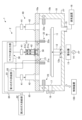
- FIG. 1 is a schematic cross-sectional diagram showing a configuration example of a plasma processing apparatus according to an embodiment.
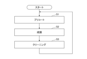
- 1 is a flowchart illustrating an example of precoating, film formation, and cleaning processing according to an embodiment.
- 5 is a time chart showing an example of a film forming process according to a reference example and an embodiment.
- 1 is a flowchart illustrating an example of a film forming process according to an embodiment.
- FIG. 3 is a diagram illustrating an example of the effect (particle reduction) of a film forming process according to an embodiment.
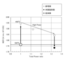
- FIG. 3 is a diagram illustrating an example of the effect (WER) of a film formation process according to an embodiment.
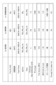
- FIG. 3 is a diagram illustrating an example of an effect of a film forming process according to an embodiment.
- FIG. 1 is a diagram showing a configuration example of a plasma processing apparatus 1 including a microwave plasma source according to an embodiment.
- the plasma processing apparatus 1 includes a processing container 10 and a plasma source 2.
- the processing container 10 has a substantially cylindrical shape made of a metal material such as aluminum and is airtight, and is grounded.
- the plasma source 2 introduces microwaves into the processing container 10 to form surface wave plasma.
- the top wall 10a of the processing container 10 is constructed by fitting dielectric members (hereinafter referred to as dielectric windows 56) of a plurality of microwave radiation sources 42 into a metal main body. Thereby, the plasma source 2 introduces microwaves into the processing chamber 10 through the plurality of dielectric windows 56 on the top wall 10a.
- the plasma processing apparatus 1 has a control device 130.
- the control device 130 is, for example, a computer, and has a program storage section (not shown).
- the program storage unit stores a program for controlling processing of a substrate W, an example of which is a semiconductor wafer, in the plasma processing apparatus 1.
- the above program may be recorded on a computer-readable storage medium such as a computer-readable hard disk (HD), flexible disk (FD), compact disk (CD), magnetic optical desk (MO), or memory card. It may be installed in the control device 130 from the storage medium.
- a mounting table 11 for horizontally supporting the substrate W is provided inside the processing container 10 and is supported by a cylindrical support member 12 erected at the center of the bottom of the processing container 10 with an insulating member 12 a interposed therebetween. ing.
- the material constituting the mounting table 11 and the support member 12 is, for example, a metal such as aluminum whose surface is alumite-treated (anodized), or an insulating material (ceramics, etc.) having a high-frequency electrode inside.
- the mounting table 11 is provided with a temperature control mechanism, a gas flow path for supplying a heat transfer gas to the back surface of the substrate W, a lifting pin that moves up and down to transport the substrate W, and the like. It is being Furthermore, an electrostatic chuck for electrostatically adsorbing the substrate W may be provided.
- an RF bias power source 14 is electrically connected to the mounting table 11 via a matching box 13. By supplying RF bias power from this RF bias power supply 14 to the mounting table 11, ions in the plasma are drawn toward the substrate W, contributing to improvement of film quality and in-plane uniformity.
- An exhaust pipe 15 is connected to the bottom side of the processing container 10, and an exhaust device 16 including a vacuum pump is connected to the exhaust pipe 15.
- an exhaust device 16 including a vacuum pump is connected to the exhaust pipe 15.
- the inside of the processing container 10 can be evacuated, and the inside of the processing container 10 can be depressurized and set to a predetermined pressure.
- the side wall 10b of the processing container 10 is provided with a loading/unloading port 17 for loading/unloading the substrate W, and a gate valve 18 for opening/closing the loading/unloading port 17.
- the plasma processing apparatus 1 includes a first gas shower section 21 for discharging a predetermined gas into the processing container 10 from the top wall 10a of the processing container 10. It also has a second gas shower section 22 that has a nozzle hanging down from the ceiling wall 10a of the processing container 10 and introduces gas from a position between the ceiling wall 10a and the mounting table 11. Furthermore, the plasma processing apparatus 1 has a nozzle that protrudes inward from the side wall 10b in the processing container 10, and is located between the side wall 10b and the mounting table 11 and from a position outside the second gas shower section 22. It has a third gas shower section 23 that introduces gas. Although the first gas shower section 21 and the second gas shower section 22 are shown at positions shifted in the radial direction for convenience in FIG. 1, they are provided alternately on the same circle.
- the first gas shower section 21 is provided on the ceiling wall 10a of the processing container 10, and has a gas supply hole 21a that supplies gas from the ceiling wall 10a. Gas carried from the first gas supply section 81 through the gas line 83 is supplied from the gas supply hole 21a at the first position.
- the second gas shower section 22 has a nozzle that hangs down from the top wall 10a of the processing container 10 and a gas supply hole 22a that supplies gas from the tip of the nozzle. Gas carried from the second gas supply section 82 through the gas line 84 is supplied from the gas supply hole 22a at the second position, which indicates the position of the tip of the nozzle. The second position is lower than the first position.
- the gas supply hole 22a is an example of a first gas supply hole that supplies gas from the ceiling wall 10a.
- the third gas shower section 23 is provided on the side wall 10b of the processing container 10, and has a nozzle that projects inward from the side wall 10b and a gas supply hole 23a that supplies gas from the tip of the nozzle. Gas carried from the second gas supply section 82 through the gas line 85 is supplied from the gas supply hole 23a at the third position, which is the tip of the nozzle. The third position is provided on the outer peripheral side of the first position and the second position.
- the gas supply hole 23a is an example of a second gas supply hole supplied from the side wall 10b.
- Raw material gas (film-forming gas) is supplied from the second gas shower section 22 and the third gas shower section 23 .
- silane (SiH 4 ) gas which is an example of a source gas, is supplied from the second gas shower section 22 and the third gas shower section 23 .
- the raw material gas may be supplied from at least one of the second gas shower section 22 and the third gas shower section 23.
- the reaction gas may be supplied from at least one of the first gas shower section 21, the second gas shower section 22, and the third gas shower section 23.
- a nitrogen-containing gas which is an example of a reaction gas, is supplied from at least one of the first gas shower section 21, the second gas shower section 22, and the third gas shower section 23.
- the nitrogen-containing gas may be ammonia (NH 3 ) gas, nitrogen (N 2 ) gas, or a combination of nitrogen (N 2 ) gas and hydrogen (H 2 ) gas. Alternatively, a mixture of these gases may be used.
- the plasma source 2 includes a microwave output section 30 that outputs microwaves by distributing them to multiple paths, and a microwave transmission section 40 that transmits the microwaves output from the microwave output section 30.
- the plasma source 2 is an example of an electromagnetic wave source that applies electromagnetic wave power.
- the microwave output section 30 includes a microwave power source, a microwave oscillator, an amplifier, and a distributor.
- the microwave power supply supplies power to the microwave oscillator.
- the microwave oscillator generates, for example, PLL oscillation of microwaves having a predetermined frequency (for example, 860 MHz).
- the amplifier amplifies the oscillated microwave.
- the distributor distributes the microwaves amplified by the amplifier while matching the impedance between the input and output sides to minimize microwave loss. Note that as the frequency of the microwave, in addition to 860 MHz, various frequencies in the range of 700 MHz to 3 GHz, such as 915 MHz, can be used.
- the microwave transmission section 40 includes a plurality of amplifier sections 41 and a plurality of microwave radiation sources 42 provided corresponding to the amplifier sections 41.
- the microwave radiation sources 42 are arranged, for example, one at the center of the ceiling wall 10a, and six at equal intervals on the circumference around the center, for a total of seven microwave radiation sources.
- the microwave radiation sources 42 at the center and the microwave radiation sources 42 at the outer periphery are arranged so that the distance between them is equal to the distance between the microwave radiation sources 42 at the outer periphery. .
- the amplifier section 41 guides the microwaves distributed by the distributor to each microwave radiation source 42.
- the microwave radiation source 42 has a coaxial tube 51 .
- the coaxial tube 51 has a coaxial microwave transmission path consisting of a cylindrical outer conductor 51a and a rod-shaped inner conductor 51b provided at the center thereof.
- the microwave radiation source 42 includes a feeding antenna (not shown) that feeds the microwave amplified by the amplifier section 41 to the coaxial tube 51. Further, the microwave radiation source 42 includes a tuner that matches the impedance of the load to the characteristic impedance of the microwave power source, and an antenna section that radiates the microwave from the coaxial tube into the processing container 10.
- the antenna section is provided at the lower end of the coaxial tube 51, and is fitted into the metal part of the top wall 10a of the processing container 10.
- the antenna section has a dielectric window 56 , and the microwaves transmitted through the dielectric window 56 generate surface wave plasma in a portion directly below the dielectric window 56 in the processing container 10 .
- a plurality of microwave radiation sources 42 are provided, one at the center of the ceiling and six at the outer periphery.
- Each of the plurality of microwave radiation sources 42 can independently control the microwave power supplied from each microwave radiation source 42.
- the microwave power supplied from the microwave radiation source 42 (dielectric window 56) at the outer periphery may be higher than or the same as the microwave power supplied from the microwave radiation source 42 at the center. Good too.
- the film forming method of this embodiment can be executed in the plasma processing apparatus 1 that supplies microwave power from the microwave radiation source 42 disposed on the top wall of the processing container 10.
- the film forming method of this embodiment is not limited to the configuration of the plasma processing apparatus 1 shown in FIG. 1, and may be performed using a plasma CVD (Chemical Vapor Deposition) apparatus or a plasma ALD (Atomic Layer Deposition) apparatus.
- FIG. 2 is a flowchart illustrating an example of precoating, film formation, and cleaning processing according to one embodiment.
- FIG. 3 is a time chart showing an example of a film forming process according to a reference example and an embodiment.
- FIG. 4 is a flowchart illustrating an example of a film forming process according to an embodiment.
- step S1 the control device 130 executes a pre-coating process to form a protective film inside the processing container 10 of the plasma processing apparatus 1.
- a protective film is formed inside the processing container 10 of a new plasma processing apparatus 1, or a protective film is formed inside the processing container 10 of the plasma processing apparatus 1 after a cleaning step, which will be described later.
- the protective film may be of the same type as the film formed in the next film forming step, or may be of a different type.
- a protective film of the same SiN film may be formed on the wall surface of the processing chamber 10 and the like in the precoating process of step S1.
- a silicon nitride film may be formed when forming a SiC film, SiO film, SiON film, etc. in the film forming process of step S2.
- step S2 the control device 130 executes a film forming process in the processing container 10 of the plasma processing apparatus 1.
- the film forming process will be described later (see FIGS. 3 and 4).
- a predetermined number of substrates are processed in the film forming process.
- the control device 130 executes a dry cleaning process for cleaning the inside of the processing container 10 of the plasma processing apparatus 1.
- a processing gas containing a fluorine-containing gas is supplied into the processing container 10, and microwave power is applied from a plurality of microwave radiation sources 42.
- plasma of the processing gas is generated in the processing container 10, and the inside of the processing container 10 is cleaned by exposing the inside of the processing container 10 to the plasma of the processing gas.
- the fluorine-containing gas include NF 3 gas.
- a mixed gas of NF 3 gas and diluting gas inert gas
- the set temperature of the mounting table 11 on which the substrate is placed is the same temperature.
- the set temperature is 450°C or lower. If the mounting table 11 is controlled to different set temperatures in the film forming process and the cleaning process, temperature control will take time and throughput will deteriorate. However, in this embodiment, since the set temperature is the same in the film forming process and the cleaning process, temperature control does not take much time and throughput can be improved.
- step S3 After the cleaning process in step S3, the process returns to step S1, and a protective film of SiN film is again formed in the processing chamber 10 after cleaning, and in step S2, a film forming process is performed to form a SiN film on the next substrate.
- FIG. 3(a) shows a film forming process of a reference example
- FIG. 3(b) shows a film forming process of this embodiment.
- argon (Ar) gas is supplied which functions as an ignition gas, but in the film forming process of this embodiment, argon gas is not supplied.
- argon (Ar) gas, ammonia (NH 3 ) gas, and silane (SiH 4 ) gas are used at time t 0 according to the procedure set in the recipe. supply will start at the same time. While supplying these gases, microwave (MW) power is applied at time t1 .
- Argon gas primarily functions to stabilize ignition and discharge. This ignites the plasma. Silane gas is a raw material gas, and ammonia gas is a reaction gas. A SiN film is formed using silane gas and ammonia gas.
- the horizontal axis indicates the number of wafers (substrates), and the vertical axis indicates the number of particles.
- the number of particles generated during processing of the first substrate was about 500.
- the number of particles increased to more than 1,000 on the second substrate, and rapidly increased to about 5,500 on the 10th substrate.
- the temperature of the mounting table 11 during film formation is set at 550° C., and gas and microwaves are supplied according to the procedure shown in FIG. 3(a).
- the film formation process is performed, a SiN film with good film quality can be obtained.
- the next cleaning process is performed at 550° C., which is the same temperature as the film forming temperature, the wall surface of the processing container 10 will be damaged, the maintenance cycle will be shortened, and productivity will deteriorate. Therefore, it is necessary to control the temperature of the mounting table 11 at 550° C. during film formation, and lower the temperature of the mounting table 11 to 450° C. during cleaning.
- the set temperatures during film formation and cleaning are different, it takes time to control the temperature of the mounting table 11, which reduces productivity.
- a method for forming a SiN film that has high productivity and can form a SiN film with excellent etching resistance.
- the cleaning process is performed by controlling the temperature to the same 450°C or lower.
- Ar gas is not supplied (not used) as an ignition gas during film formation so that a high quality SiN film can be obtained even if the temperature of the mounting table 11 is set to 450° C. or lower.
- FIG. 3B shows that in the film forming process of this embodiment, supply of ammonia (NH 3 ) gas is started at time t 0 according to the procedure set in the recipe. While supplying ammonia gas, microwave (MW) power is applied at time t1 . Plasma is ignited by ammonia gas. After a predetermined time T has elapsed from time t1 , silane (SiH 4 ) gas is supplied. This forms a SiN film.
- NH 3 ammonia
- MW microwave
- Plasma is ignited by ammonia gas.
- silane (SiH 4 ) gas is supplied. This forms a SiN film.
- the predetermined time T from time t1 to time t2 is a step of stabilizing the plasma, and is, for example, 1 second to 5 seconds.
- the plasma becomes unstable for a short period of time after ignition until the matching stabilizes.
- the silane gas exists at a high partial pressure, particles will be generated.
- argon gas is not used. Therefore, the partial pressure of silane gas with respect to all gases is higher than in the case of the reference example using argon gas. Therefore, the number of particles tends to increase.
- ammonia gas is supplied at time t0 , and this ammonia gas is also used as ignition gas. Then, after a predetermined time T has elapsed since microwaves were supplied and plasma was ignited, silane gas is supplied, and ammonia gas is made to function as a reaction gas in the silane gas of the film-forming gas to form a SiN film. This eliminates the instability of microwaves and reduces the number of particles. Moreover, this makes it possible to form a SiN film with good etching resistance (hydrofluoric acid resistance).
- FIG. 5(b) is an enlarged view of the number of particles B in FIG. 5(a). According to this, even if SiN films were formed on 50 substrates without intervening a cleaning process, the number of particles on each substrate was approximately 100 or less.
- the method for forming a SiN film according to the present embodiment since argon gas is not used, it is difficult to damage the inside of the processing container 10. As a result, after one precoating process, 25 to 50 substrates can be processed without performing a cleaning process. This makes it possible to lengthen the cleaning cycle, increase throughput, and improve productivity. Furthermore, in this embodiment, since the set temperature is the same during film formation and during cleaning, it does not take much time to control the temperature of the mounting table 11. Furthermore, a good quality SiN film can be obtained even when the film is formed by setting the temperature of the mounting table 11 to 450° C. or lower. As described above, according to the method for forming a SiN film according to the present embodiment, it is possible to form a SiN film with high productivity and excellent etching resistance.
- silane gas is supplied from the edge and center of the processing container 10.
- the silane gas supplied from the edge of the processing container 10 is silane gas supplied from the third gas shower section 23 of the side wall 10b of the processing container 10.
- the silane gas supplied from the center of the processing container 10 is silane gas supplied from the second gas shower section 22 on the top wall 10a of the processing container 10.
- control device 130 prepares a substrate in the processing container 10 in step S11.
- control device 130 supplies ammonia gas into the processing container 10.
- the control device 130 After supplying the ammonia gas, in step S13, the control device 130 applies microwave power, which is an example of electromagnetic waves. By applying the microwave power, the control device 130 ignites the ammonia gas plasma in step S ⁇ b>14 to generate the ammonia gas plasma in the processing container 10 .
- step S15 the control device 130 determines whether the predetermined time T has elapsed.
- the control device 130 waits until the predetermined time T has elapsed, and when determining that the predetermined time T has elapsed, proceeds to step S16.
- step S16 the control device 130 introduces silane gas into the processing container 10 from the second gas shower section 22 (from the center).
- step S17 the control device 130 introduces silane gas into the processing container 10 from the third gas shower section 23 (from the edge), and in step S18, causes the silane gas to react with the ammonia gas plasma so that it is applied onto the substrate. Form a SiN film.
- step S16 and step S17 may be executed simultaneously, or step S17 may be executed before step S16.
- the ratio of the flow rates of the silane gas supplied from the second gas shower section 22 (gas supply hole 22a) and the silane gas supplied from the third gas shower section 23 (gas supply hole 23a) is, for example, within the range of 1:1 to 1:5.
- the flow rate of silane gas (e-SiH 4 ) supplied from the edge is greater than the flow rate of silane gas (c-SiH 4 ) supplied from the center, and is supplied simultaneously.
- step S19 the processed substrate is carried out.
- step S20 the control device 130 determines whether a predetermined number of films have been deposited.
- the predetermined number of sheets may be set within the range of 25 to 50 sheets as shown in the particle reduction effect of this embodiment in FIG. 5(b).
- step S20 if the control device 130 determines that the predetermined number of substrates have not been continuously deposited, the control device 130 returns to step S11, carries in the next unprocessed substrate, and executes the processes of steps S11 to S19 on the next substrate. do.
- step S20 if the control device 130 determines that a predetermined number of films have been continuously deposited, this process ends.
- a SiN film with good etching resistance and high quality can be formed using ammonia gas and silane gas without using argon gas. Further, the cleaning cycle can be lengthened, and the throughput can be increased while maintaining the film quality of the SiN film, and productivity can be improved.
- the pressure inside the processing container 10 is controlled to about 10 Pa, and the plasma is ignited.
- the pressure inside the processing container 10 may be controlled to a higher pressure within a range of greater than 10 Pa and less than or equal to 20 Pa. Thereby, plasma can be ignited more stably.
- the set temperature (film forming temperature) of the mounting table 11 is controlled to the same temperature of 450° C. or lower. Even at such a low temperature, it is possible to form a SiN film of the same quality as the SiN film formed by controlling the set temperature of the mounting table 11 to 550°C.
- FIG. 6 is a diagram illustrating an example of the effect (WER) of temperature control and film formation processing according to one embodiment.
- the horizontal axis in FIG. 6 shows the ratio of the total power of microwaves applied from the seven microwave radiation sources 42, and the vertical axis shows WER (wet etch rate).
- WER on the vertical axis indicates the amount ( ⁇ /min) that can be removed in one minute when immersed in a solution diluted with hydrofluoric acid at a concentration of 0.5%.
- the ratio of the total power of microwaves on the horizontal axis indicates the process conditions in the reference example and the conventional SiN film formation method before increasing the power, with the set temperature of the film formation process and cleaning process being 550°C in the conventional example.
- the total power of the microwaves applied from the seven microwave radiation sources 42 when set at 450° C. is assumed to be 1, and the ratio of the total power of the microwaves to this is shown.
- the process conditions of the reference example and the conventional example before increasing the power are that in the film forming process and the cleaning process, the set temperature of the mounting table 11 in the reference example is 450°C, whereas in the conventional example, the setting temperature of the mounting table 11 is 450°C.
- the set temperature of the stand 11 is 550°C.
- the SiN film formed under the conditions of the reference example had higher WER and worse etching resistance than the SiN film formed under the conditions of the conventional example. This is considered to be because the set temperature of the mounting table 11 was lowered to 450° C. in the reference example.
- the process conditions of this embodiment are such that the set temperature of the mounting table 11 is controlled at 450°C, and ammonia gas is used as the ignition gas without using argon gas, as shown in FIG. 3(b).
- a SiN film was formed according to the procedure shown.
- the SiN film according to this embodiment was able to reduce the WER to a level equal to or higher than that of the SiN film under the conventional process conditions.
- a gas containing argon gas that is, SiH 4 gas, NH 3 gas, and Ar gas
- the set temperature of the mounting table 11 is set to 450°C.
- the SiN film was formed by controlling the total power to 3,500 to 4,000 W.
- argon gas is not used as the ignition gas, only ammonia gas is used, the set temperature of the mounting table 11 is set to 450°C, and the total power is set to 3500 W ⁇
- a SiN film was formed by controlling the power to 4000W.
- the total power is the total power of microwaves applied from seven microwave radiation sources 42.
- the film thickness uniformity (Thickness Non-Uniformity) was all around 1, the film thickness uniformity was the same, and the film thickness of all SiN films was uniform.
- SiN film forming method and plasma processing apparatus should be considered to be illustrative in all respects and not restrictive.
- the embodiments can be modified and improved in various ways without departing from the scope and spirit of the appended claims.
- the matters described in the plurality of embodiments described above may be configured in other ways without being inconsistent, and may be combined without being inconsistent.
- Plasma processing apparatus 2 Plasma source 10 Processing container 11 Mounting table 42 Microwave radiation source 130 Control device
Landscapes
- Chemical & Material Sciences (AREA)
- Engineering & Computer Science (AREA)
- Metallurgy (AREA)
- Chemical Kinetics & Catalysis (AREA)
- Materials Engineering (AREA)
- Mechanical Engineering (AREA)
- General Chemical & Material Sciences (AREA)
- Organic Chemistry (AREA)
- Physics & Mathematics (AREA)
- Plasma & Fusion (AREA)
- Inorganic Chemistry (AREA)
- Analytical Chemistry (AREA)
- Chemical Vapour Deposition (AREA)
- Formation Of Insulating Films (AREA)
- Drying Of Semiconductors (AREA)
Abstract
Description
本実施形態に係る成膜方法を実行するプラズマ処理装置の構成例について、図1を参照して説明する。図1は、一実施形態に係るマイクロ波のプラズマ源を備えたプラズマ処理装置1の構成例を示す図である。
次に、一実施形態に係るプリコート、成膜、クリーニング処理について、図2~図4を参照しながら説明する。図2は、一実施形態に係るプリコート、成膜、クリーニング処理の一例を示すフローチャートである。図3は、参考例及び一実施形態に係る成膜処理の一例を示すタイムチャートである。図4は、一実施形態に係る成膜処理の一例を示すフローチャートである。
ステップS2の成膜工程について、図3~図5を参照しながら詳述する。図3(a)は参考例の成膜工程を示し、図3(b)は本実施形態の成膜工程を示す。参考例の成膜工程では着火ガスとして機能するアルゴン(Ar)ガスを供給するが、本実施形態の成膜工程ではアルゴンガスを供給しない。
本実施形態に係る成膜工程(SiN膜の形成工程)の一実施例について、図4を参照しながら説明する。図4に示す一実施形態に係る成膜処理の実施例では、処理容器10のエッジとセンターからシランガスを供給する例を挙げて説明する。処理容器10のエッジから供給されるシランガスは、処理容器10の側壁10bの第3のガスシャワー部23から供給されるシランガスである。処理容器10のセンターから供給されるシランガスは、処理容器10の天壁10aの第2のガスシャワー部22から供給されるシランガスである。
本実施形態では、図2の成膜工程(S2)とクリーニング工程(S3)とでは、載置台11の設定温度(成膜温度)をいずれも450℃又はそれ以下の同一温度に制御する。係る低温であっても、載置台11の設定温度を550℃に制御して成膜したSiN膜と同等の膜質のSiN膜を形成することができる。
図7を参照して、一実施形態に係る成膜処理の効果の一例について説明する。前述した「(a)従来例」のプロセス条件では、着火ガスにアルゴンガスを含むガス、すなわち、図7の「Ignition」に示したSiH4ガス、NH3ガス、Arガスを使用し、載置台11の設定温度を550℃に設定し、トータルのパワーを2500W~3000Wに制御し、SiN膜を形成した。これに対して「(b)参考例」のプロセス条件では、着火ガスにアルゴンガスを含むガス、すなわち、SiH4ガス、NH3ガス、Arガスを使用し、載置台11の設定温度を450℃に設定し、トータルのパワーを3500~4000Wに制御し、SiN膜を形成した。また、「(c)本実施形態」のプロセス条件では、着火ガスにアルゴンガスを使用せず、アンモニアガスのみを使用し、載置台11の設定温度を450℃に設定し、トータルパワーを3500W~4000Wに制御し、SiN膜を形成した。トータルパワーは、7本のマイクロ波放射源42から印加されるマイクロ波の総電力である。
2 プラズマ源
10 処理容器
11 載置台
42 マイクロ波放射源
130 制御装置
Claims (17)
- 処理容器内に基板を準備する工程と、
前記処理容器内に窒素含有ガスを供給する工程と、
前記窒素含有ガスの供給後に電磁波の電力を印加して前記処理容器内に窒素含有ガスのプラズマを生成する工程と、
前記窒素含有ガスのプラズマを生成後、前記処理容器内にシリコン含有原料ガスを供給して前記窒素含有ガスのプラズマと反応させて前記基板上にSiN膜を形成する工程と、
を備える、SiN膜の形成方法。 - 前記電磁波の電力の印加と前記シリコン含有原料ガスの供給との間にプラズマを安定させる工程をさらに含む、
請求項1記載のSiN膜の形成方法。 - プラズマを安定させる工程は1秒~5秒の範囲内である
請求項2記載のSiN膜の形成方法。 - 前記処理容器は、天壁からガスを供給する第1のガス供給孔と、側壁から供給する第2のガス供給孔と、を備え、
前記シリコン含有原料ガスは、前記第1のガス供給孔と前記第2のガス供給孔とから供給される、
請求項1~請求項3のいずれか1項に記載のSiN膜の形成方法。 - 前記第1のガス供給孔から供給される前記シリコン含有原料ガスと、前記第2のガス供給孔から供給される前記シリコン含有原料ガスと、の流量の比率は、1:1~1:5の範囲内である、
請求項4に記載のSiN膜の形成方法。 - 前記シリコン含有原料ガスは、前記第1のガス供給孔から供給した後、前記第2のガス供給孔から供給される、
請求項4に記載のSiN膜の形成方法。 - 前記シリコン含有原料ガスは、前記第1のガス供給孔と前記第2のガス供給孔とから同時に供給される、
請求項4に記載のSiN膜の形成方法。 - 前記電磁波は、複数のマイクロ波放射源から印加される、
請求項1~請求項3のいずれか1項に記載のSiN膜の形成方法。 - 前記SiN膜を形成する工程において、前記基板を載置する載置台の設定温度を450℃以下に設定し、かつ、前記設定温度を550℃に設定したときに複数の前記マイクロ波放射源から印加されるマイクロ波の総電力を1としたときの1.3倍~1.4倍の範囲内のマイクロ波の総電力を印加する、
請求項8に記載のSiN膜の形成方法。 - 所定の枚数の前記基板にSiN膜を形成した後、前記処理容器内にフッ素含有ガスを含む処理ガスを供給し、複数の前記マイクロ波放射源からマイクロ波の電力を印加して前記処理容器内に前記処理ガスのプラズマを生成して、前記処理ガスのプラズマにさらすことで前記処理容器内をクリーニングする工程をさらに備える、
請求項8に記載のSiN膜の形成方法。 - 前記所定の枚数は、25枚~50枚である、
請求項10に記載のSiN膜の形成方法。 - 前記SiN膜を形成する工程及び前記処理容器内をクリーニングする工程において、前記基板を載置する載置台の設定温度は同一温度である、
請求項9に記載のSiN膜の形成方法。 - 前記設定温度は、450℃以下である、
請求項12に記載のSiN膜の形成方法。 - 処理容器内をクリーニングする工程の後、前記処理容器内に保護膜を形成する工程をさらに備える、
請求項10に記載のSiN膜の形成方法。 - 前記保護膜は、SiN膜である、
請求項14に記載のSiN膜の形成方法。 - 前記保護膜を形成する工程は、前記SiN膜を形成する工程と同じプロセス条件で行う、
請求項14に記載のSiN膜の形成方法。 - 処理容器と、
電磁波の電力を印加する電磁波源と、
ガスを供給するガス供給源と、制御装置と、を備えるプラズマ処理装置であって、
前記制御装置は、
処理容器内に基板を準備する工程と、
前記処理容器内に窒素含有ガスを供給する工程と、
前記窒素含有ガスの供給後に電磁波の電力を印加して前記処理容器内に窒素含有ガスのプラズマを生成する工程と、
前記窒素含有ガスのプラズマを生成後、前記処理容器内にシリコン含有原料ガスを供給して前記窒素含有ガスのプラズマと反応させて前記基板上にSiN膜を形成する工程と、
を制御する、プラズマ処理装置。
Priority Applications (2)
| Application Number | Priority Date | Filing Date | Title |
|---|---|---|---|
| KR1020257006668A KR20250042824A (ko) | 2022-08-02 | 2023-07-06 | SiN막의 형성 방법 및 플라즈마 처리 장치 |
| US19/024,424 US20250154649A1 (en) | 2022-08-02 | 2025-01-16 | Silicon nitride film formation method and plasma processing apparatus |
Applications Claiming Priority (2)
| Application Number | Priority Date | Filing Date | Title |
|---|---|---|---|
| JP2022-123217 | 2022-08-02 | ||
| JP2022123217A JP2024020777A (ja) | 2022-08-02 | 2022-08-02 | SiN膜の形成方法及びプラズマ処理装置 |
Related Child Applications (1)
| Application Number | Title | Priority Date | Filing Date |
|---|---|---|---|
| US19/024,424 Continuation US20250154649A1 (en) | 2022-08-02 | 2025-01-16 | Silicon nitride film formation method and plasma processing apparatus |
Publications (1)
| Publication Number | Publication Date |
|---|---|
| WO2024029271A1 true WO2024029271A1 (ja) | 2024-02-08 |
Family
ID=89849221
Family Applications (1)
| Application Number | Title | Priority Date | Filing Date |
|---|---|---|---|
| PCT/JP2023/025190 Ceased WO2024029271A1 (ja) | 2022-08-02 | 2023-07-06 | SiN膜の形成方法及びプラズマ処理装置 |
Country Status (4)
| Country | Link |
|---|---|
| US (1) | US20250154649A1 (ja) |
| JP (1) | JP2024020777A (ja) |
| KR (1) | KR20250042824A (ja) |
| WO (1) | WO2024029271A1 (ja) |
Citations (5)
| Publication number | Priority date | Publication date | Assignee | Title |
|---|---|---|---|---|
| JPS6281032A (ja) * | 1985-10-03 | 1987-04-14 | Matsushita Electric Ind Co Ltd | 半導体装置の製造方法 |
| JPS6437028A (en) * | 1987-08-03 | 1989-02-07 | Japan Synthetic Rubber Co Ltd | Manufacture of semiconductor element |
| JP2014038874A (ja) * | 2010-11-08 | 2014-02-27 | Canon Anelva Corp | プラズマ誘起cvd方法 |
| JP2021125566A (ja) * | 2020-02-05 | 2021-08-30 | 東京エレクトロン株式会社 | プラズマ処理装置及びガス流量調整方法 |
| JP2021166250A (ja) * | 2020-04-07 | 2021-10-14 | 東京エレクトロン株式会社 | クリーニング方法およびプラズマ処理装置 |
Family Cites Families (4)
| Publication number | Priority date | Publication date | Assignee | Title |
|---|---|---|---|---|
| JP4777717B2 (ja) | 2005-08-10 | 2011-09-21 | 東京エレクトロン株式会社 | 成膜方法、プラズマ処理装置および記録媒体 |
| CN101517713B (zh) | 2006-09-19 | 2011-02-09 | 东京毅力科创株式会社 | 等离子体清洁方法和等离子体cvd方法 |
| JP2014060378A (ja) | 2012-08-23 | 2014-04-03 | Tokyo Electron Ltd | シリコン窒化膜の成膜方法、有機電子デバイスの製造方法及びシリコン窒化膜の成膜装置 |
| JP6861479B2 (ja) | 2016-06-24 | 2021-04-21 | 東京エレクトロン株式会社 | プラズマ成膜方法およびプラズマ成膜装置 |
-
2022
- 2022-08-02 JP JP2022123217A patent/JP2024020777A/ja active Pending
-
2023
- 2023-07-06 KR KR1020257006668A patent/KR20250042824A/ko active Pending
- 2023-07-06 WO PCT/JP2023/025190 patent/WO2024029271A1/ja not_active Ceased
-
2025
- 2025-01-16 US US19/024,424 patent/US20250154649A1/en active Pending
Patent Citations (5)
| Publication number | Priority date | Publication date | Assignee | Title |
|---|---|---|---|---|
| JPS6281032A (ja) * | 1985-10-03 | 1987-04-14 | Matsushita Electric Ind Co Ltd | 半導体装置の製造方法 |
| JPS6437028A (en) * | 1987-08-03 | 1989-02-07 | Japan Synthetic Rubber Co Ltd | Manufacture of semiconductor element |
| JP2014038874A (ja) * | 2010-11-08 | 2014-02-27 | Canon Anelva Corp | プラズマ誘起cvd方法 |
| JP2021125566A (ja) * | 2020-02-05 | 2021-08-30 | 東京エレクトロン株式会社 | プラズマ処理装置及びガス流量調整方法 |
| JP2021166250A (ja) * | 2020-04-07 | 2021-10-14 | 東京エレクトロン株式会社 | クリーニング方法およびプラズマ処理装置 |
Also Published As
| Publication number | Publication date |
|---|---|
| KR20250042824A (ko) | 2025-03-27 |
| JP2024020777A (ja) | 2024-02-15 |
| US20250154649A1 (en) | 2025-05-15 |
Similar Documents
| Publication | Publication Date | Title |
|---|---|---|
| KR102690416B1 (ko) | 성막 방법 및 성막 장치 | |
| US12018375B2 (en) | Flim forming method of carbon-containing film by microwave plasma | |
| US10957515B2 (en) | Plasma processing method and plasma processing apparatus | |
| CN101310367A (zh) | 等离子体蚀刻方法 | |
| JP3946640B2 (ja) | プラズマ処理装置およびプラズマ処理方法 | |
| US12534800B2 (en) | Pre-coating method and processing apparatus | |
| US20220316065A1 (en) | Processing apparatus and film forming method | |
| JP2001189308A (ja) | プラズマ処理装置及びプラズマ処理方法 | |
| WO2024029271A1 (ja) | SiN膜の形成方法及びプラズマ処理装置 | |
| US20230062105A1 (en) | Film forming method and film forming apparatus | |
| JP4059792B2 (ja) | 半導体製造方法 | |
| US11335542B2 (en) | Plasma processing apparatus | |
| US20250299924A1 (en) | Substrate processing method and substrate processing apparatus | |
| JP7341099B2 (ja) | クリーニング方法およびプラズマ処理装置 | |
| JP7814200B2 (ja) | 成膜装置および成膜方法 | |
| US20250389018A1 (en) | Silicon carbonitride film-forming method and plasma processing apparatus | |
| US20230061151A1 (en) | Film forming method and film forming apparatus | |
| US20240240307A1 (en) | Method of forming silicon nitride film | |
| JP2023180078A (ja) | 成膜方法及びプラズマ処理装置 | |
| JP2001011641A (ja) | 成膜処理方法 | |
| JP2023157446A (ja) | プラズマ処理方法、プラズマ処理装置、およびステージ | |
| JP2023131713A (ja) | 成膜方法及び処理装置 | |
| CN116334594A (zh) | 基板处理方法及利用pecvd的氮化硅膜沉积方法 | |
| WO2025110012A1 (ja) | 半導体装置の製造方法および製造システム | |
| JPH11238727A (ja) | プラズマcvd装置 |
Legal Events
| Date | Code | Title | Description |
|---|---|---|---|
| 121 | Ep: the epo has been informed by wipo that ep was designated in this application |
Ref document number: 23849830 Country of ref document: EP Kind code of ref document: A1 |
|
| ENP | Entry into the national phase |
Ref document number: 20257006668 Country of ref document: KR Kind code of ref document: A |
|
| NENP | Non-entry into the national phase |
Ref country code: DE |
|
| WWP | Wipo information: published in national office |
Ref document number: 1020257006668 Country of ref document: KR |
|
| 122 | Ep: pct application non-entry in european phase |
Ref document number: 23849830 Country of ref document: EP Kind code of ref document: A1 |