WO2024024382A1 - 積層セラミックコンデンサ - Google Patents
積層セラミックコンデンサ Download PDFInfo
- Publication number
- WO2024024382A1 WO2024024382A1 PCT/JP2023/024153 JP2023024153W WO2024024382A1 WO 2024024382 A1 WO2024024382 A1 WO 2024024382A1 JP 2023024153 W JP2023024153 W JP 2023024153W WO 2024024382 A1 WO2024024382 A1 WO 2024024382A1
- Authority
- WO
- WIPO (PCT)
- Prior art keywords
- main surface
- hydrophobic
- hydrophilic
- section
- surface side
- Prior art date
- Legal status (The legal status is an assumption and is not a legal conclusion. Google has not performed a legal analysis and makes no representation as to the accuracy of the status listed.)
- Ceased
Links
Images


Classifications
-
- H—ELECTRICITY
- H01—ELECTRIC ELEMENTS
- H01G—CAPACITORS; CAPACITORS, RECTIFIERS, DETECTORS, SWITCHING DEVICES, LIGHT-SENSITIVE OR TEMPERATURE-SENSITIVE DEVICES OF THE ELECTROLYTIC TYPE
- H01G4/00—Fixed capacitors; Processes of their manufacture
- H01G4/30—Stacked capacitors
-
- H—ELECTRICITY
- H01—ELECTRIC ELEMENTS
- H01G—CAPACITORS; CAPACITORS, RECTIFIERS, DETECTORS, SWITCHING DEVICES, LIGHT-SENSITIVE OR TEMPERATURE-SENSITIVE DEVICES OF THE ELECTROLYTIC TYPE
- H01G4/00—Fixed capacitors; Processes of their manufacture
- H01G4/002—Details
- H01G4/005—Electrodes
- H01G4/012—Form of non-self-supporting electrodes
-
- H—ELECTRICITY
- H01—ELECTRIC ELEMENTS
- H01G—CAPACITORS; CAPACITORS, RECTIFIERS, DETECTORS, SWITCHING DEVICES, LIGHT-SENSITIVE OR TEMPERATURE-SENSITIVE DEVICES OF THE ELECTROLYTIC TYPE
- H01G4/00—Fixed capacitors; Processes of their manufacture
- H01G4/002—Details
- H01G4/018—Dielectrics
- H01G4/06—Solid dielectrics
- H01G4/08—Inorganic dielectrics
- H01G4/12—Ceramic dielectrics
- H01G4/1209—Ceramic dielectrics characterised by the ceramic dielectric material
-
- H—ELECTRICITY
- H01—ELECTRIC ELEMENTS
- H01G—CAPACITORS; CAPACITORS, RECTIFIERS, DETECTORS, SWITCHING DEVICES, LIGHT-SENSITIVE OR TEMPERATURE-SENSITIVE DEVICES OF THE ELECTROLYTIC TYPE
- H01G4/00—Fixed capacitors; Processes of their manufacture
- H01G4/002—Details
- H01G4/018—Dielectrics
- H01G4/06—Solid dielectrics
- H01G4/14—Organic dielectrics
- H01G4/18—Organic dielectrics of synthetic material, e.g. derivatives of cellulose
-
- H—ELECTRICITY
- H01—ELECTRIC ELEMENTS
- H01G—CAPACITORS; CAPACITORS, RECTIFIERS, DETECTORS, SWITCHING DEVICES, LIGHT-SENSITIVE OR TEMPERATURE-SENSITIVE DEVICES OF THE ELECTROLYTIC TYPE
- H01G4/00—Fixed capacitors; Processes of their manufacture
- H01G4/002—Details
- H01G4/224—Housing; Encapsulation
-
- H—ELECTRICITY
- H01—ELECTRIC ELEMENTS
- H01G—CAPACITORS; CAPACITORS, RECTIFIERS, DETECTORS, SWITCHING DEVICES, LIGHT-SENSITIVE OR TEMPERATURE-SENSITIVE DEVICES OF THE ELECTROLYTIC TYPE
- H01G4/00—Fixed capacitors; Processes of their manufacture
- H01G4/002—Details
- H01G4/228—Terminals
- H01G4/232—Terminals electrically connecting two or more layers of a stacked or rolled capacitor
-
- H—ELECTRICITY
- H01—ELECTRIC ELEMENTS
- H01G—CAPACITORS; CAPACITORS, RECTIFIERS, DETECTORS, SWITCHING DEVICES, LIGHT-SENSITIVE OR TEMPERATURE-SENSITIVE DEVICES OF THE ELECTROLYTIC TYPE
- H01G4/00—Fixed capacitors; Processes of their manufacture
- H01G4/002—Details
- H01G4/018—Dielectrics
- H01G4/06—Solid dielectrics
- H01G4/08—Inorganic dielectrics
- H01G4/12—Ceramic dielectrics
- H01G4/1209—Ceramic dielectrics characterised by the ceramic dielectric material
- H01G4/1218—Ceramic dielectrics characterised by the ceramic dielectric material based on titanium oxides or titanates
- H01G4/1227—Ceramic dielectrics characterised by the ceramic dielectric material based on titanium oxides or titanates based on alkaline earth titanates
-
- H—ELECTRICITY
- H01—ELECTRIC ELEMENTS
- H01G—CAPACITORS; CAPACITORS, RECTIFIERS, DETECTORS, SWITCHING DEVICES, LIGHT-SENSITIVE OR TEMPERATURE-SENSITIVE DEVICES OF THE ELECTROLYTIC TYPE
- H01G4/00—Fixed capacitors; Processes of their manufacture
- H01G4/002—Details
- H01G4/018—Dielectrics
- H01G4/06—Solid dielectrics
- H01G4/08—Inorganic dielectrics
- H01G4/12—Ceramic dielectrics
- H01G4/1209—Ceramic dielectrics characterised by the ceramic dielectric material
- H01G4/1236—Ceramic dielectrics characterised by the ceramic dielectric material based on zirconium oxides or zirconates
-
- H—ELECTRICITY
- H01—ELECTRIC ELEMENTS
- H01G—CAPACITORS; CAPACITORS, RECTIFIERS, DETECTORS, SWITCHING DEVICES, LIGHT-SENSITIVE OR TEMPERATURE-SENSITIVE DEVICES OF THE ELECTROLYTIC TYPE
- H01G4/00—Fixed capacitors; Processes of their manufacture
- H01G4/002—Details
- H01G4/228—Terminals
- H01G4/232—Terminals electrically connecting two or more layers of a stacked or rolled capacitor
- H01G4/2325—Terminals electrically connecting two or more layers of a stacked or rolled capacitor characterised by the material of the terminals
-
- Y—GENERAL TAGGING OF NEW TECHNOLOGICAL DEVELOPMENTS; GENERAL TAGGING OF CROSS-SECTIONAL TECHNOLOGIES SPANNING OVER SEVERAL SECTIONS OF THE IPC; TECHNICAL SUBJECTS COVERED BY FORMER USPC CROSS-REFERENCE ART COLLECTIONS [XRACs] AND DIGESTS
- Y02—TECHNOLOGIES OR APPLICATIONS FOR MITIGATION OR ADAPTATION AGAINST CLIMATE CHANGE
- Y02E—REDUCTION OF GREENHOUSE GAS [GHG] EMISSIONS, RELATED TO ENERGY GENERATION, TRANSMISSION OR DISTRIBUTION
- Y02E60/00—Enabling technologies; Technologies with a potential or indirect contribution to GHG emissions mitigation
- Y02E60/13—Energy storage using capacitors
Definitions
- the present invention relates to a multilayer ceramic capacitor.
- a method for solving electrochemical migration for example, there is a method of forming a silane coupling treatment film on the surface of an electronic component by silane coupling treatment.
- this silane coupling agent In order to exhibit high water repellency with this silane coupling agent, it is possible to lengthen the linear chain of the silane coupling agent.
- the linear chain of this silane coupling agent is lengthened, the steric hindrance caused by this linear chain increases, and the distance between the silane coupling agents arranged on the surface of electronic components becomes wider, which reduces the density of the silane coupling agent. It will drop.
- the effect of suppressing dew condensation is not sufficient, dew condensation occurs on the surface of the electronic component between the silane coupling agents, and electrochemical migration occurs due to the above-mentioned generation process.
- Patent Document 1 proposes a method of suppressing the above-mentioned ion migration using a perfluoroalkylalkylsilane-based water repellent treatment agent, that is, a silane coupling agent having F (fluorine) as a functional group. ing.
- a perfluoroalkylalkylsilane-based water repellent treatment agent that is, a silane coupling agent having F (fluorine) as a functional group.
- Patent Document 1 does not sufficiently suppress electrochemical migration. That is, when a silane coupling agent having F as a functional group is used, steric hindrance due to the linear chain of the silane coupling agent can be reduced and higher water repellency can be expressed, but the density is not sufficient.
- the water repellent treatment is only performed by adding a water repellent agent, and the area to which the water repellent agent is not added is not subjected to hydrophilic treatment.
- the difference in the contact angle of water with the added portion may be small, and a sufficient water repellent effect may not be obtained.
- An object of the present invention is to provide a multilayer ceramic capacitor that can suppress the occurrence of electrochemical migration.
- a multilayer ceramic capacitor according to the present invention includes a plurality of stacked dielectric layers, and has a first main surface and a second main surface facing each other in the height direction, and a first main surface and a second main surface facing each other in the width direction orthogonal to the height direction.
- a laminate having a first side surface and a second side surface, and a first end surface and a second end surface facing each other in a length direction perpendicular to a height direction and a width direction; a first internal electrode layer disposed on the plurality of dielectric layers and exposed on the second end surface; a second internal electrode layer disposed on the plurality of dielectric layers and exposed on the second end surface; A multilayer ceramic capacitor comprising a first external electrode disposed on an end face of the multilayer ceramic capacitor, and a second external electrode disposed on the second end face of the multilayer ceramic capacitor.
- a hydrophobic part is arranged, and the hydrophilic part is arranged on at least a part of the first main surface, and the hydrophilic part on the first main surface side having a hydroxyl group, and at least one part on the second main surface.
- a second main surface-side hydrophilic portion having a hydroxyl group and located on the first side surface; a first side-side hydrophilic portion having a hydroxyl group and located on at least a portion of the first side surface; a second side-side hydrophilic portion having a hydroxyl group, the hydrophobic portion being located on at least a portion of the first main surface and containing fluorine or silicone.
- first main surface side hydrophobic part a first main surface side hydrophobic part, a second main surface side hydrophobic part disposed on at least a part of the second main surface and containing fluorine or silicone, and at least one part on the first side surface.
- FIG. 1 is an external oblique view of a multilayer ceramic capacitor according to a first embodiment.
- FIG. 2 is a cross-sectional view of the multilayer ceramic capacitor shown in FIG. 1 taken along line II-II.
- 3 is a sectional view taken along line III-III of the multilayer ceramic capacitor shown in FIG. 2.
- FIG. FIG. 3 is a cross-sectional view of the multilayer ceramic capacitor shown in FIG. 2 taken along line IVA-IVA.
- FIG. 3 is a cross-sectional view of the multilayer ceramic capacitor shown in FIG. 2 taken along line IVB-IVB.
- FIG. 3 is a cross-sectional view of the multilayer ceramic capacitor shown in FIG. 2 taken along line VV.
- FIG. 3 is a cross-sectional view of the multilayer ceramic capacitor shown in FIG.
- FIG. 2 is an arrow diagram when the multilayer ceramic capacitor shown in FIG. 1 is viewed from the first main surface side along the direction of arrow VII.
- FIG. 2 is a diagram showing a multilayer ceramic capacitor with a double-layer structure.
- FIG. 3 is a diagram showing a multilayer ceramic capacitor with a triple structure.
- FIG. 3 is a diagram showing a multilayer ceramic capacitor with a quadruple structure.
- 8 is a diagram showing a multilayer ceramic capacitor according to a second embodiment, and corresponds to FIG. 7.
- FIG. FIG. 2 is a diagram showing a multilayer ceramic capacitor according to a second embodiment, and is an arrow diagram when looking at the second main surface side along the direction of arrow X shown in FIG. 1.
- FIG. 8 is a diagram showing a multilayer ceramic capacitor according to a third embodiment, and corresponds to FIG. 7.
- FIG. 8 is a diagram showing a multilayer ceramic capacitor according to a fourth embodiment, and corresponds to FIG. 7.
- FIG. 13 is a hypothetical arrow diagram when the multilayer ceramic capacitor shown in FIG. 12 is viewed from the second end face side along the direction of arrow XIII.
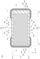
- FIG. 1 is an external perspective view of a multilayer ceramic capacitor 1 according to this embodiment.
- FIG. 2 is a cross-sectional view of the multilayer ceramic capacitor 1 of FIG. 1 taken along line II-II.
- FIG. 3 is a cross-sectional view of the multilayer ceramic capacitor 1 of FIG. 2 taken along line III-III.
- FIG. 4A is a cross-sectional view of the multilayer ceramic capacitor 1 of FIG. 2 taken along the line IVA-IVA.
- FIG. 4B is a cross-sectional view of the multilayer ceramic capacitor 1 of FIG. 2 taken along the line IVB-IVB.
- the multilayer ceramic capacitor 1 includes a multilayer body 10 and an external electrode 40.
- FIGS. 1 to 4B An XYZ orthogonal coordinate system is shown in FIGS. 1 to 4B.
- the length direction L of the multilayer ceramic capacitor 1 and the multilayer body 10 corresponds to the X direction.
- the width direction W of the multilayer ceramic capacitor 1 and the multilayer body 10 corresponds to the Y direction.
- the height direction T of the multilayer ceramic capacitor 1 and the multilayer body 10 corresponds to the Z direction.
- the cross section shown in FIG. 2 is also referred to as the LT cross section.
- the cross section shown in FIG. 3 is also referred to as a WT cross section.
- the cross sections shown in FIGS. 4A and 4B are also referred to as LW cross sections.
- the laminate 10 has a first main surface TS1 and a second main surface TS2 facing in the height direction T and facing in the width direction W perpendicular to the height direction T. It includes a first side surface WS1 and a second side surface WS2, and a first end surface LS1 and a second end surface LS2 that face each other in the length direction L perpendicular to the height direction T and the width direction W.
- the laminate 10 has a substantially rectangular parallelepiped shape.
- the dimension of the laminate 10 in the length direction L is not necessarily longer than the dimension in the width direction W. It is preferable that the corners and ridges of the laminate 10 be rounded.
- a corner is a part where three sides of the laminate intersect, and a ridgeline is a part where two sides of the laminate intersect. Incidentally, unevenness may be formed on a part or all of the surface constituting the laminate 10.
- a hydrophilic portion 80 and a hydrophobic portion 70 are arranged on the surface of the laminate 10.
- the hydrophilic portion 80 and the hydrophobic portion 70 will be described later.
- the surface of the laminate 10 is formed by a first main surface TS1, a second main surface TS2, a first side surface WS1, a second side surface WS2, a first end surface LS1, and a second end surface LS2. Ru.
- the laminate 10 includes an inner layer part 11, a first main surface side outer layer part 12 and a second main surface arranged to sandwich the inner layer part 11 in the height direction T. It has a side outer layer part 13.
- the inner layer section 11 includes a plurality of dielectric layers 20 and a plurality of internal electrode layers 30.
- the inner layer portion 11 includes, in the height direction T, an internal electrode layer 30 located closest to the first main surface TS1 to an internal electrode layer 30 located closest to the second main surface TS2.
- a plurality of internal electrode layers 30 are arranged facing each other with the dielectric layer 20 interposed therebetween.
- the inner layer portion 11 is a portion that generates capacitance and essentially functions as a capacitor.
- the plurality of dielectric layers 20 are made of dielectric material.
- the dielectric material may be, for example, a dielectric ceramic containing components such as BaTiO 3 , CaTiO 3 , SrTiO 3 or CaZrO 3 . Further, the dielectric material may be one in which subcomponents such as Mn compounds, Fe compounds, Cr compounds, Co compounds, and Ni compounds are added to these main components. It is particularly preferred that the dielectric material is a material containing BaTiO 3 as a main component.
- the thickness of the dielectric layer 20 is preferably 0.5 ⁇ m or more and 10 ⁇ m or less.
- the number of dielectric layers 20 to be laminated is preferably 15 or more and 1200 or less. Note that the number of dielectric layers 20 is the total number of dielectric layers in the inner layer section 11 and the number of dielectric layers in the first main surface side outer layer section 12 and the second main surface side outer layer section 13. be.
- the plurality of internal electrode layers 30 have a plurality of first internal electrode layers 31 and a plurality of second internal electrode layers 32.
- the plurality of first internal electrode layers 31 are arranged on the plurality of dielectric layers 20.
- the plurality of second internal electrode layers 32 are arranged on the plurality of dielectric layers 20.
- the plurality of first internal electrode layers 31 and the plurality of second internal electrode layers 32 are alternately arranged in the height direction T of the stacked body 10 with the dielectric layers 20 interposed therebetween.
- the first internal electrode layer 31 and the second internal electrode layer 32 are arranged with the dielectric layer 20 sandwiched therebetween.
- the first internal electrode layer 31 includes a first opposing portion 31A that faces the second internal electrode layer 32, and a first drawn-out portion 31B that is drawn out from the first opposing portion 31A to the first end surface LS1. have.
- the first drawer portion 31B is exposed at the first end surface LS1.
- the second internal electrode layer 32 includes a second opposing portion 32A that faces the first internal electrode layer 31, and a second drawn-out portion 32B that is drawn out from the second opposing portion 32A to the second end surface LS2. have.
- the second drawer portion 32B is exposed at the second end surface LS2.
- a capacitance is formed by the first opposing portion 31A and the second opposing portion 32A facing each other with the dielectric layer 20 in between, and the characteristics of a capacitor are exhibited.
- the shapes of the first opposing portion 31A and the second opposing portion 32A are not particularly limited, but are preferably rectangular. However, the rectangular corner portions may be rounded, or the rectangular corner portions may be formed obliquely.
- the shapes of the first drawer part 31B and the second drawer part 32B are not particularly limited, but are preferably rectangular. However, the rectangular corner portions may be rounded, or the rectangular corner portions may be formed obliquely.
- the dimension in the width direction W of the first facing portion 31A and the dimension in the width direction W of the first drawer portion 31B may be formed to be the same dimension, or one of the dimensions may be formed smaller.
- the dimension in the width direction W of the second facing portion 32A and the dimension in the width direction W of the second drawer portion 32B may be the same, or one of the dimensions may be formed narrower. .
- the first internal electrode layer 31 and the second internal electrode layer 32 are made of an appropriate conductive material such as a metal such as Ni, Cu, Ag, Pd, or Au, or an alloy containing at least one of these metals. be done. When using an alloy, the first internal electrode layer 31 and the second internal electrode layer 32 may be made of, for example, an Ag--Pd alloy.
- each of the first internal electrode layer 31 and the second internal electrode layer 32 is preferably about 0.2 ⁇ m or more and 2.0 ⁇ m or less, for example.
- the total number of first internal electrode layers 31 and second internal electrode layers 32 is preferably 15 or more and 1000 or less.
- the first main surface side outer layer portion 12 is located on the first main surface TS1 side of the laminate 10.
- the first main surface side outer layer portion 12 is an aggregate of a plurality of dielectric layers 20 located between the first main surface TS1 and the internal electrode layer 30 closest to the first main surface TS1.
- the dielectric layer 20 used in the first main surface side outer layer section 12 may be the same as the dielectric layer 20 used in the inner layer section 11.
- the second main surface side outer layer portion 13 is located on the second main surface TS2 side of the laminate 10.
- the second main surface side outer layer portion 13 is an aggregate of a plurality of dielectric layers 20 located between the second main surface TS2 and the internal electrode layer 30 closest to the second main surface TS2.
- the dielectric layer 20 used in the second main surface side outer layer portion 13 may be the same as the dielectric layer 20 used in the inner layer portion 11.
- the laminate 10 includes a plurality of stacked dielectric layers 20 and a plurality of internal electrode layers 30 stacked on the dielectric layers 20. That is, the multilayer ceramic capacitor 1 has a multilayer body 10 in which dielectric layers 20 and internal electrode layers 30 are alternately stacked.
- the laminate 10 has a counter electrode portion 11E.
- the opposing electrode portion 11E is a portion where the first opposing portion 31A of the first internal electrode layer 31 and the second opposing portion 32A of the second internal electrode layer 32 face each other.
- the counter electrode section 11E is configured as a part of the inner layer section 11. 4A and 4B show the range in the width direction W and length direction L of the counter electrode portion 11E. Note that the counter electrode portion 11E is also referred to as a capacitor effective portion.
- the laminate 10 has a side surface side outer layer portion.
- the side surface side outer layer portion includes a first side surface side outer layer portion WG1 and a second side surface side outer layer portion WG2.
- the first side surface side outer layer portion WG1 is a portion including the dielectric layer 20 located between the counter electrode portion 11E and the first side surface WS1.
- the second side surface side outer layer portion WG2 is a portion including the dielectric layer 20 located between the counter electrode portion 11E and the second side surface WS2.
- FIG. 4A, and FIG. 4B show the range in the width direction W of the first side-side outer layer portion WG1 and the second side-side outer layer portion WG2.
- the side surface side outer layer portion is also referred to as a W gap or a side gap.
- the laminate 10 has an outer layer portion on the end surface side.
- the end surface side outer layer portion includes a first end surface side outer layer portion LG1 and a second end surface side outer layer portion LG2.
- the first end surface side outer layer portion LG1 is a portion including the dielectric layer 20 located between the counter electrode portion 11E and the first end surface LS1.
- the second end surface side outer layer portion LG2 is a portion including the dielectric layer 20 located between the counter electrode portion 11E and the second end surface LS2.
- FIG. 4A, and FIG. 4B show the range in the length direction L of the first end surface side outer layer portion LG1 and the second end surface side outer layer portion LG2.
- the end surface side outer layer portion is also referred to as an L gap or an end gap.
- the external electrode 40 includes a first external electrode 40A arranged on the first end surface LS1 side and a second external electrode 40B arranged on the second end surface LS2 side.
- the first external electrode 40A is arranged on the first end surface LS1.
- the first external electrode 40A is connected to the first internal electrode layer 31.
- the first external electrode 40A is also arranged on a part of the first main surface TS1 and a part of the second main surface TS2, as well as a part of the first side surface WS1 and a part of the second side surface WS2. You can leave it there.
- the first external electrode 40A extends from above the first end surface LS1 to a part of the first main surface TS1 and a part of the second main surface TS2, and a part of the first side surface WS1 and It is formed to extend to a part of the second side surface WS2.
- the second external electrode 40B is arranged on the second end surface LS2.
- the second external electrode 40B is connected to the second internal electrode layer 32.
- the second external electrode 40B is also arranged on a part of the first main surface TS1 and a part of the second main surface TS2, as well as a part of the first side surface WS1 and a part of the second side surface WS2. You can leave it there.
- the second external electrode 40B extends from above the second end surface LS2 to a part of the first main surface TS1 and a part of the second main surface TS2, and a part of the first side surface WS1 and It is formed to extend to a part of the second side surface WS2.
- the first opposing portion 31A of the first internal electrode layer 31 and the second opposing portion 32A of the second internal electrode layer 32 are opposed to each other with the dielectric layer 20 in between. This creates a capacitance. Therefore, capacitor characteristics are developed between the first external electrode 40A to which the first internal electrode layer 31 is connected and the second external electrode 40B to which the second internal electrode layer 32 is connected.
- the first external electrode 40A includes a first base electrode layer 50A and a first plating layer 60A disposed on the first base electrode layer 50A.
- the second external electrode 40B includes a second base electrode layer 50B and a second plating layer 60B disposed on the second base electrode layer 50B.
- the first base electrode layer 50A is arranged on the first end surface LS1.
- the first base electrode layer 50A is connected to the first internal electrode layer 31.
- the first base electrode layer 50A extends from above the first end surface LS1 to a part of the first main surface TS1, a part of the second main surface TS2, and a part of the first side surface WS1. and a part of the second side surface WS2.
- the second base electrode layer 50B is arranged on the second end surface LS2.
- the second base electrode layer 50B is connected to the second internal electrode layer 32.
- the second base electrode layer 50B extends from above the second end surface LS2 to a part of the first main surface TS1, a part of the second main surface TS2, and a part of the first side surface WS1. and a part of the second side surface WS2.
- the first base electrode layer 50A and the second base electrode layer 50B of this embodiment are baked layers.
- the baking layer contains a metal component and either a glass component or a ceramic component, or both.
- the metal component includes, for example, at least one selected from Cu, Ni, Ag, Pd, Ag-Pd alloy, Au, and the like.
- the glass component includes, for example, at least one selected from B, Si, Ba, Mg, Al, Li, and the like.
- the ceramic component the same type of ceramic material as the dielectric layer 20 may be used, or a different type of ceramic material may be used.
- the ceramic component includes, for example, at least one selected from BaTiO 3 , CaTiO 3 , (Ba,Ca)TiO 3 , SrTiO 3 , CaZrO 3 , and the like.
- the baked layer is, for example, a layered product coated with a conductive paste containing glass and metal and baked.
- the baked layer may be obtained by simultaneously firing a multilayer chip having internal electrodes and a dielectric layer and a conductive paste applied to the multilayer chip, or by baking a multilayer chip having internal electrodes and a dielectric layer to obtain a multilayer body.
- the laminate may then be coated with a conductive paste and baked.
- the baked layer is formed by baking a layer to which a ceramic material is added instead of a glass component. It is preferable. In this case, it is particularly preferable to use the same type of ceramic material as the dielectric layer 20 as the added ceramic material.
- the baking layer may have multiple layers.
- the thickness in the length direction of the first base electrode layer 50A located on the first end surface LS1 is, for example, 10 ⁇ m or more and 150 ⁇ m or less at the center of the first base electrode layer 50A in the height direction T and width direction W. It is preferable that the degree of
- the thickness in the length direction of the second base electrode layer 50B located on the second end surface LS2 is, for example, 10 ⁇ m or more and 150 ⁇ m or less at the center of the second base electrode layer 50B in the height direction T and width direction W. It is preferable that the degree of
- the first base electrode layer 50A When the first base electrode layer 50A is also provided on a part of at least one of the first main surface TS1 or the second main surface TS2, the first base electrode layer 50A provided on this part
- the thickness in the height direction T is preferably, for example, approximately 10 ⁇ m or more and 100 ⁇ m or less at the central portion in the length direction L and width direction W of the first base electrode layer 50A provided in this portion.
- the width of the first base electrode layer 50A provided on this part is preferably, for example, approximately 10 ⁇ m or more and 100 ⁇ m or less in the central portion in the length direction L and height direction T of the first base electrode layer 50A provided in this portion.
- the second base electrode layer 50B When the second base electrode layer 50B is also provided on a part of at least one of the first main surface TS1 or the second main surface TS2, the second base electrode layer 50B provided on this part
- the thickness in the height direction T is preferably, for example, approximately 10 ⁇ m or more and 100 ⁇ m or less at the central portion in the length direction L and width direction W of the second base electrode layer 50B provided in this portion.
- the width of the second base electrode layer 50B provided on this part is preferably, for example, approximately 10 ⁇ m or more and 100 ⁇ m or less in the central portion in the length direction L and height direction T of the second base electrode layer 50B provided in this portion.
- first base electrode layer 50A and the second base electrode layer 50B are not limited to baked layers.
- the first base electrode layer 50A and the second base electrode layer 50B include at least one selected from a baked layer, a conductive resin layer, a thin film layer, and the like.
- the first base electrode layer 50A and the second base electrode layer 50B may be thin film layers.
- the thin film layer is formed by a thin film forming method such as a sputtering method or a vapor deposition method.
- the thin film layer is a layer of 10 ⁇ m or less on which metal particles are deposited.
- the first plating layer 60A is arranged to cover the first base electrode layer 50A.
- the second plating layer 60B is arranged to cover the second base electrode layer 50B.
- the first plating layer 60A and the second plating layer 60B may contain at least one selected from Cu, Ni, Sn, Ag, Pd, Ag-Pd alloy, Au, etc., for example.
- the first plating layer 60A and the second plating layer 60B may each be formed of multiple layers.
- the first plating layer 60A and the second plating layer 60B preferably have a two-layer structure in which a Sn plating layer is formed on a Ni plating layer.
- the first plating layer 60A is arranged to cover the first base electrode layer 50A.
- the first plating layer 60A includes a first Ni plating layer 61A and a first Sn plating layer 62A located on the first Ni plating layer 61A.
- the second plating layer 60B is arranged to cover the second base electrode layer 50B.
- the second plating layer 60B includes a second Ni plating layer 61B and a second Sn plating layer 62B located on the second Ni plating layer 61B.
- the Ni plating layer prevents the first base electrode layer 50A and the second base electrode layer 50B from being eroded by solder when mounting the multilayer ceramic capacitor 1. Furthermore, the Sn plating layer improves solder wettability when mounting the multilayer ceramic capacitor 1. This facilitates mounting of the multilayer ceramic capacitor 1.
- the thickness of each of the first Ni plating layer 61A, the first Sn plating layer 62A, the second Ni plating layer 61B, and the second Sn plating layer 62B is preferably 1 ⁇ m or more and 15 ⁇ m or less.
- first external electrode 40A and the second external electrode 40B of this embodiment may have a conductive resin layer containing, for example, a conductive filler and a thermosetting resin.
- the conductive resin layer may be disposed to cover the baked layer, or may be disposed to cover the baked layer. It may also be placed directly on the laminate 10 without providing any.
- the conductive resin layer is arranged to cover the baked layer, the conductive resin layer is arranged between the baked layer and the plating layer (first plating layer 60A, second plating layer 60B).
- the conductive resin layer may completely cover the baking layer or may partially cover the baking layer.
- a conductive resin layer containing a thermosetting resin is more flexible than a conductive layer made of, for example, a plated film or a fired product of a conductive paste. Therefore, even if the multilayer ceramic capacitor 1 is subjected to a physical impact or an impact caused by a thermal cycle, the conductive resin layer functions as a buffer layer. Therefore, the conductive resin layer suppresses the occurrence of cracks in the multilayer ceramic capacitor 1.
- the metal constituting the conductive filler may be Ag, Cu, Ni, Sn, Bi, or an alloy containing them.
- the conductive filler preferably contains Ag.
- the conductive filler is, for example, Ag metal powder. Ag has the lowest specific resistance among metals, so it is suitable as an electrode material. Furthermore, since Ag is a noble metal, it is difficult to oxidize and has high weather resistance. Therefore, Ag metal powder is suitable as a conductive filler.
- the conductive filler may be a metal powder whose surface is coated with Ag.
- the metal powder is preferably Cu, Ni, Sn, Bi, or an alloy powder thereof. It is preferable to use Ag-coated metal powder in order to make the base metal inexpensive while maintaining the properties of Ag.
- the conductive filler may be Cu or Ni subjected to oxidation prevention treatment. Further, the conductive filler may be a metal powder whose surface is coated with Sn, Ni, or Cu. When using metal powder whose surface is coated with Sn, Ni, or Cu, the metal powder is preferably Ag, Cu, Ni, Sn, Bi, or an alloy powder thereof.
- the shape of the conductive filler is not particularly limited.
- the conductive filler may be spherical or flat, but it is preferable to use a mixture of spherical metal powder and flat metal powder.
- the average particle diameter of the conductive filler is not particularly limited.
- the average particle diameter of the conductive filler may be, for example, 0.3 ⁇ m or more and 10 ⁇ m or less.
- the conductive filler contained in the conductive resin layer is preferably contained in an amount of 35 vol% or more and 75 vol% or less with respect to the volume of the entire conductive resin layer.
- the conductive filler contained in the conductive resin layer mainly plays the role of ensuring the conductivity of the conductive resin layer. Specifically, when a plurality of conductive fillers come into contact with each other, a current-carrying path is formed inside the conductive resin layer.
- the resin constituting the conductive resin layer may include at least one selected from various known thermosetting resins such as epoxy resin, phenol resin, urethane resin, silicone resin, and polyimide resin.
- epoxy resin which has excellent heat resistance, moisture resistance, and adhesion, is one of the most suitable resins.
- the resin of the conductive resin layer contains a curing agent together with the thermosetting resin.
- the curing agent for the epoxy resin may be various known compounds such as phenol type, amine type, acid anhydride type, imidazole type, active ester type, amideimide type, etc.
- the conductive resin layer may be formed of multiple layers.
- the thickness of the thickest part of the conductive resin layer is preferably 10 ⁇ m or more and 200 ⁇ m or less.
- the multilayer ceramic capacitor 1 may include a plating layer that is directly electrically connected to the first internal electrode layer 31 and the second internal electrode layer 32. In such a case, the plating layer may be formed after disposing a catalyst on the surface of the laminate 10 as a pretreatment.
- the plating layer has multiple layers. It is preferable that the lower plating layer and the upper plating layer each contain at least one metal selected from, for example, Cu, Ni, Sn, Pb, Au, Ag, Pd, Bi, or Zn, or an alloy containing these metals. . More preferably, the lower plating layer is formed using Ni, which has solder barrier properties. The upper plating layer is more preferably formed using Sn or Au, which has good solder wettability. Note that, for example, when the first internal electrode layer 31 and the second internal electrode layer 32 are formed using Ni, the lower plating layer may be formed using Cu, which has good bonding properties with Ni. preferable.
- the upper plating layer may be formed as necessary, and the external electrode 40 may be composed of only the lower plating layer.
- the plating layer may have the upper plating layer as the outermost layer, or may further form another plating layer on the surface of the upper plating layer.
- each plating layer arranged without a base electrode layer is preferably 1 ⁇ m or more and 15 ⁇ m or less. Note that the plating layer preferably does not contain glass.
- the metal ratio per unit volume of the plating layer is preferably 99% by volume or more.
- the thickness of the base electrode layer can be reduced. Therefore, by reducing the thickness of the base electrode layer, the dimension in the height direction T of the multilayer ceramic capacitor 1 can be reduced, and the height of the multilayer ceramic capacitor 1 can be reduced.
- the thickness of the dielectric layer 20 sandwiched between the first internal electrode layer 31 and the second internal electrode layer 32 is made thicker to compensate for the reduction in the thickness of the base electrode layer, thereby improving the element thickness. Can be done. By forming the plating layer directly on the laminate 10 in this way, the degree of freedom in designing the multilayer ceramic capacitor can be improved.
- the L dimension is preferably 0.2 mm or more and 10 mm or less.
- the T dimension is preferably 0.1 mm or more and 5 mm or less.
- the W dimension is 0.1 mm or more and 10 mm or less.
- a hydrophobic portion 70 and a hydrophilic portion 80 are arranged on the surface of the laminate 10 in order to suppress the occurrence of electrochemical migration.
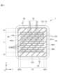
- FIG. 5 is a cross-sectional view of the multilayer ceramic capacitor 1 shown in FIG. 2 taken along the line VV.
- FIG. 6 is a cross-sectional view of the multilayer ceramic capacitor 1 shown in FIG. 2 taken along the line VI-VI.
- FIG. 7 is an arrow diagram when the multilayer ceramic capacitor 1 shown in FIG. 1 is viewed from the first main surface TS1 side along the direction of arrow VII.
- the outline of the laminated body 10 covered with the hydrophobic part 70, the hydrophilic part 80, and the external electrode 40 is shown with a broken line.
- the hydrophobic portion 70 is a hydrophobic layer placed on the surface of the laminate 10.
- the hydrophobic portion 70 is formed by coating the laminate 10 with, for example, a fluorine-based silane coupling material.
- one hydrophobic portion 70 is arranged on the surface of the laminate 10.
- the hydrophobic portion 70 includes a first main surface side hydrophobic portion 71, a second main surface side hydrophobic portion 72, It has a first side hydrophobic portion 73 and a second side hydrophobic portion 74 .
- the first main surface side hydrophobic portion 71 is a hydrophobic layer containing at least one of fluorine and silicone.
- the first main surface side hydrophobic portion 71 is arranged on at least a portion of the first main surface TS1. Specifically, as shown in FIG. 2, the first main surface side hydrophobic portion 71 is located in a region TE1 located between the first external electrode 40A and the second external electrode 40B on the first main surface TS1. placed within.
- the first main surface side hydrophobic portion 71 is arranged so as to extend in a strip-like shape in the width direction W at the center of the laminate 10 in the length direction L. As shown in FIGS. 1, 5, and 7, the first main surface side hydrophobic portion 71 extends from the end on the first side surface WS1 side in the width direction W on the first main surface TS1 to the second It is arranged over the end on the side surface WS2 side.
- the second main surface side hydrophobic portion 72 is a hydrophobic layer containing at least one of fluorine and silicone.
- the second main surface side hydrophobic portion 72 is arranged on at least a portion of the second main surface TS2. Specifically, as shown in FIG. 2, the second main surface side hydrophobic portion 72 is located in a region TE2 located between the first external electrode 40A and the second external electrode 40B on the second main surface TS2. placed within.
- the second main surface side hydrophobic portion 72 is arranged so as to extend in the width direction W in a strip-like manner at the center of the laminate 10 in the length direction L. As shown in FIG. 5, the second main surface side hydrophobic portion 72 extends from an end on the first side surface WS1 side to an end on the second side surface WS2 side in the width direction W on the second main surface TS2. placed across.
- the first side hydrophobic portion 73 is a hydrophobic layer containing at least one of fluorine and silicone.
- the first side surface hydrophobic portion 73 is arranged on at least a portion of the first side surface WS1. Specifically, as shown in FIGS. 4A and 4B, the first side hydrophobic portion 73 is a region located between the first external electrode 40A and the second external electrode 40B on the first side surface WS1. It is located in WE1. That is, the first side surface side hydrophobic portion 73 is arranged between the first external electrode 40A and the second external electrode 40B on the first side surface WS1.
- the first side hydrophobic portion 73 is arranged so as to extend in the height direction T in a strip-like manner at the center of the laminate 10 in the length direction L.
- the first side surface side hydrophobic portion 73 is arranged from an end on the first main surface TS1 side to an end on the second main surface TS2 side in the height direction T on the first side surface WS1.
- the second side hydrophobic portion 74 is a hydrophobic layer containing at least one of fluorine and silicone.
- the second side surface side hydrophobic portion 74 is arranged on at least a portion of the second side surface WS2. Specifically, as shown in FIGS. 4A and 4B, the second side surface side hydrophobic portion 74 is a region located between the first external electrode 40A and the second external electrode 40B on the second side surface WS2. Located within WE2.
- the second side-side hydrophobic portion 74 is arranged so as to extend in the height direction T in a strip-like manner at the center of the laminate 10 in the length direction L.
- the second side surface side hydrophobic portion 74 is arranged from an end on the first main surface TS1 side to an end on the second main surface TS2 side in the height direction T on the second side surface WS2.
- the hydrophobic portion 70 of this embodiment as shown in FIG. and are arranged continuously via the second side hydrophobic portion 74.
- the first side hydrophobic part 73 and the second side hydrophobic part 74 are arranged continuously via the first main surface hydrophobic part 71, and the second main surface hydrophobic part 72 is connected to the first side hydrophobic part 73. are arranged consecutively through the That is, the hydrophobic portion 70 has a ring shape as a whole, and is arranged across the first main surface TS1, the second main surface TS2, the first side surface WS1, and the second side surface WS2 of the laminate 10. .
- the hydrophobic portion 70 is arranged on the surface of the laminate 10, when water droplets W are generated due to dew condensation, it is possible to suppress the water droplets from wetting and spreading on the surface of the laminate 10. Therefore, formation of a water droplet path, which is a water film spanning between the first external electrode 40A and the second external electrode 40B, can be suppressed.
- the hydrophilic portion 80 is a hydrophilic layer placed on the surface of the laminate 10.
- the hydrophilic portion 80 is formed by applying, for example, a hydroxyl group-containing silane coupling material to the laminate 10.
- two hydrophilic portions 80a and 80b which are two hydrophilic portions 80, are arranged on the surface of the laminate 10.
- the hydrophilic portion 80a is located between the first external electrode 40A and the hydrophobic portion 70 on the first main surface TS1, the second main surface TS2, the first side surface WS1, and the second side surface WS2.
- the hydrophilic portion 80b is arranged between the hydrophobic portion 70 and the second external electrode 40B on the first main surface TS1, the second main surface TS2, the first side surface WS1, and the second side surface WS2. That is, the hydrophobic portion 70 is sandwiched between the hydrophilic portions 80 in the length direction L.
- each hydrophilic part 80 includes a first main surface side hydrophilic part 81 and a second main surface side hydrophilic part 82. , a first side hydrophilic portion 83 and a second side hydrophilic portion 84 .
- the first main surface side hydrophilic portion 81 is a hydrophilic layer having hydroxyl groups.
- the first main surface side hydrophilic portion 81 is arranged on at least a portion of the first main surface TS1.
- the first main surface side hydrophilic portion 81 is a region located between the first external electrode 40A and the second external electrode 40B on the first main surface TS1, as shown in FIG. Located within TE1.
- the first main surface side hydrophilic section 81 of the hydrophilic section 80a is arranged between the first external electrode 40A and the hydrophobic section 70 on the first main surface TS1.
- the first main surface side hydrophilic section 81 of the hydrophilic section 80a is arranged so as to cover the entire surface between the first external electrode 40A and the hydrophobic section 70 on the first main surface TS1. . That is, the first main surface side hydrophilic section 81 of the hydrophilic section 80 a is arranged so as to be in contact with the first main surface side hydrophobic section 71 of the hydrophobic section 70 . Further, the first main surface side hydrophilic section 81 of the hydrophilic section 80b is arranged between the hydrophobic section 70 and the second external electrode 40B on the first main surface TS1.
- the first main surface side hydrophilic section 81 of the hydrophilic section 80b is arranged so as to cover the entire surface between the hydrophobic section 70 and the second external electrode 40B on the first main surface TS1. . That is, the first main surface side hydrophilic section 81 of the hydrophilic section 80b is arranged so as to be in contact with the first main surface side hydrophobic section 71 of the hydrophobic section 70. As shown in FIGS. 6 and 7, the first main surface side hydrophilic portion 81 extends from the end on the first side surface WS1 side in the width direction W on the first main surface TS1 to the second side surface WS2 side. It is arranged across the end.
- the second main surface side hydrophilic portion 82 is a hydrophilic layer having hydroxyl groups.
- the second main surface side hydrophilic portion 82 is arranged on at least a portion of the second main surface TS2. Specifically, as shown in FIG. 2, the second main surface side hydrophilic portion 82 is a region located between the first external electrode 40A and the second external electrode 40B on the second main surface TS2. Located within TE2. In this embodiment, the second main surface side hydrophilic section 82 of the hydrophilic section 80a is arranged between the first external electrode 40A and the hydrophobic section 70 on the second main surface TS2.
- the second main surface side hydrophilic section 82 of the hydrophilic section 80a is arranged so as to cover the entire surface between the first external electrode 40A and the hydrophobic section 70 on the second main surface TS2. . That is, the second main surface side hydrophilic section 82 of the hydrophilic section 80 a is arranged so as to be in contact with the second main surface side hydrophobic section 72 of the hydrophobic section 70 . Further, the second main surface side hydrophilic section 82 of the hydrophilic section 80b is arranged between the hydrophobic section 70 and the second external electrode 40B on the second main surface TS2.
- the second main surface side hydrophilic section 82 of the hydrophilic section 80b is arranged to cover the entire surface between the hydrophobic section 70 and the second external electrode 40B on the second main surface TS2. . That is, the second main surface side hydrophilic section 82 of the hydrophilic section 80b is arranged so as to be in contact with the second main surface side hydrophobic section 72 of the hydrophobic section 70. As shown in FIG. 6, the second main surface side hydrophilic portion 82 extends from an end on the first side surface WS1 side to an end on the second side surface WS2 side in the width direction W on the second main surface TS2. placed across.
- the first side hydrophilic portion 83 is a hydrophilic layer having hydroxyl groups.
- the first side surface hydrophilic portion 83 is arranged on at least a portion of the first side surface WS1. Specifically, the first side surface hydrophilic portion 83 is located between the first external electrode 40A and the second external electrode 40B on the first side surface WS1, as shown in FIGS. 4A and 4B. It is arranged within the area WE1.
- the first side surface side hydrophilic section 83 of the hydrophilic section 80a is arranged between the first external electrode 40A and the hydrophobic section 70 on the first side surface WS1.
- the first side surface side hydrophilic portion 83 of the hydrophilic portion 80a is arranged so as to cover the entire surface between the first external electrode 40A and the hydrophobic portion 70 on the first side surface WS1. That is, the first side hydrophilic portion 83 of the hydrophilic portion 80 a is arranged so as to be in contact with the first side hydrophobic portion 73 of the hydrophobic portion 70 . Further, the first side surface side hydrophilic portion 83 of the hydrophilic portion 80b is arranged between the hydrophobic portion 70 and the second external electrode 40B on the first side surface WS1.
- the first side surface side hydrophilic portion 83 of the hydrophilic portion 80b is arranged so as to cover the entire surface between the hydrophobic portion 70 and the second external electrode 40B on the first side surface WS1. That is, the first side hydrophilic portion 83 of the hydrophilic portion 80b is arranged so as to be in contact with the first side hydrophobic portion 73 of the hydrophobic portion 70. As shown in FIG. 6, the first side surface side hydrophilic portion 83 extends from an end on the first main surface TS1 side in the height direction T on the first side surface WS1 to an end on the second main surface TS2 side. will be placed over the
- the second side hydrophilic portion 84 is a hydrophilic layer having hydroxyl groups.
- the second side surface side hydrophilic portion 84 is arranged on at least a portion of the second side surface WS2. Specifically, the second side surface side hydrophilic portion 84 is located between the first external electrode 40A and the second external electrode 40B on the second side surface WS2, as shown in FIGS. 4A and 4B. It is arranged within the area WE2.
- the second side surface side hydrophilic section 84 of the hydrophilic section 80a is arranged between the first external electrode 40A and the hydrophobic section 70 on the second side surface WS2.
- the second side surface hydrophilic portion 84 of the hydrophilic portion 80a is arranged to cover the entire surface between the first external electrode 40A and the hydrophobic portion 70 on the second side surface WS2. That is, the second side hydrophilic portion 84 of the hydrophilic portion 80 a is arranged so as to be in contact with the second side hydrophobic portion 74 of the hydrophobic portion 70 . Further, the second side surface side hydrophilic portion 84 of the hydrophilic portion 80b is arranged between the hydrophobic portion 70 and the second external electrode 40B on the second side surface WS2.
- the second side surface hydrophilic portion 84 of the hydrophilic portion 80b is arranged to cover the entire surface between the hydrophobic portion 70 and the second external electrode 40B on the second side surface WS2. That is, the second side-side hydrophilic portion 84 of the hydrophilic portion 80b is arranged so as to be in contact with the second side-side hydrophobic portion 74 of the hydrophobic portion 70. As shown in FIG. 6, the second side surface side hydrophilic portion 84 extends from an end on the first main surface TS1 side in the height direction T on the second side surface WS2 to an end on the second main surface TS2 side. will be placed over the
- the hydrophilic portion 80 of this embodiment as shown in FIG. and are arranged continuously via the second side hydrophilic portion 84.
- the first side surface side hydrophilic section 83 and the second side side hydrophilic section 84 are arranged continuously via the first main surface side hydrophilic section 81, and the second main surface side hydrophilic section 82 is disposed in succession. are arranged consecutively through the That is, the hydrophilic portion 80 has a ring shape as a whole and is arranged over the first main surface TS1, the second main surface TS2, the first side surface WS1, and the second side surface WS2 of the laminate 10.
- the multilayer ceramic capacitor 1 according to the present embodiment, not only the hydrophobic part 70 but also the hydrophilic part 80 are arranged on the surface of the multilayer body 10 which is a ceramic body, so that as shown in FIG. , water droplets W can be guided from the hydrophobic part 70 to the hydrophilic part 80.
- the formation of a water droplet path spanning between the first external electrode 40A and the second external electrode 40B can be suppressed. Therefore, it becomes more difficult for the water droplet W to form an interelectrode path, so that deterioration due to electrochemical migration can be significantly suppressed.
- the thickness of the hydrophobic portion 70 is preferably 5 nm or more and 1000 nm or less. Thereby, water droplets W generated due to dew condensation can be guided to the hydrophilic portion 80, and formation of a water droplet path spanning between the first external electrode 40A and the second external electrode 40B can be more effectively suppressed. Note that when the thickness of the hydrophobic portion 70 is less than 5 nm, the contact angle with water decreases, and the water repellent effect decreases. If the thickness of the hydrophobic portion 70 is greater than 1000 nm, the hydrophobic material forming the hydrophobic portion 70 will adhere to the suction nozzle when inserting the laminated ceramic capacitor 1 into the taping during transportation of the multilayer ceramic capacitor 1, resulting in suction errors. It becomes easier to wake up. Note that the thickness of the hydrophobic portion 70 is determined by measuring and converting the weight, specific gravity, and surface area of the multilayer ceramic capacitor 1.
- the thickness of the hydrophilic portion 80 is preferably 10 nm or more and 500 nm or less.
- the difference between the contact angle of water at the hydrophobic portion 70 and the contact angle of water at the hydrophilic portion 80 is preferably 30° or more. It is more preferable that the difference between the contact angle of water at the hydrophobic portion 70 and the contact angle of water at the hydrophilic portion 80 is 40° or more.
- a dielectric sheet for the dielectric layer 20 and a conductive paste for the internal electrode layer 30 are prepared.
- the conductive paste for the dielectric sheet and internal electrodes contains a binder and a solvent.
- the binder and solvent may be known ones.
- a conductive paste for the internal electrode layer 30 is printed in a predetermined pattern on the dielectric sheet by, for example, screen printing or gravure printing. As a result, a dielectric sheet on which the pattern of the first internal electrode layer 31 is formed and a dielectric sheet on which the pattern of the second internal electrode layer 32 is formed are prepared.
- a laminated block is produced by pressing the laminated sheet in the height direction by means such as a hydrostatic press.
- laminated chips are cut out.
- the corners and ridges of the laminated chip may be rounded by barrel polishing or the like.
- the stacked body 10 is produced by firing the stacked chips.
- the firing temperature depends on the materials of the dielectric layer 20 and the internal electrode layer 30, it is preferably 900° C. or more and 1400° C. or less.
- a conductive paste that becomes base electrode layers (first base electrode layer 50A, second base electrode layer 50B) is applied to both end faces of the laminate 10.
- the base electrode layer is a baked layer.
- a conductive paste containing a glass component and a metal is applied to the laminate 10 by, for example, dipping. Thereafter, a baking process is performed to form a base electrode layer.
- the temperature of the baking treatment at this time is preferably 700°C or more and 900°C or less.
- the baked layer is preferably formed by baking a ceramic material added instead of a glass component.
- a ceramic material added instead of a glass component.
- a conductive paste is applied to the laminated chip before firing, and the laminated chip and the conductive paste applied to the laminated chip are simultaneously baked to form the laminated body 10 in which the baked layer is formed.
- a plating layer is formed on the surface of the base electrode layer.
- a first plating layer 60A is formed on the surface of the first base electrode layer 50A.
- a second plating layer 60B is formed on the surface of the second base electrode layer 50B.
- a Ni plating layer and a Sn plating layer are formed as the plating layers.
- electrolytic plating requires pretreatment with a catalyst or the like in order to improve the plating deposition rate, which has the disadvantage of complicating the process. Therefore, it is usually preferable to employ electrolytic plating.
- the Ni plating layer and the Sn plating layer are sequentially formed by, for example, barrel plating.
- the thin film layer as the base electrode layer is formed in the portion where the external electrode is desired to be formed by performing masking or the like.
- the thin film layer is formed by a thin film forming method such as a sputtering method or a vapor deposition method.
- the thin film layer is a layer of 1.0 ⁇ m or less on which metal particles are deposited.
- the conductive resin layer when providing a conductive resin layer as a base electrode layer, the conductive resin layer may be placed so as to cover the baking layer, or may be placed directly on the laminate 10 without providing a baking layer.
- a conductive resin paste containing a thermosetting resin and a metal component is applied onto the baking layer or the laminate 10, and then heat treated at a temperature of 250 to 550° C. or higher. Thereby, the thermosetting resin is thermosetted, and a conductive resin layer is formed.
- the atmosphere during this heat treatment is preferably a N2 atmosphere.
- the oxygen concentration is preferably 100 ppm or less.
- the plating layer may be directly placed on the exposed portion of the internal electrode layer 30 of the laminate 10 without providing the base electrode layer.
- plating is performed on the first end surface LS1 and the second end surface LS2 of the laminate 10, and a plating layer is formed on the exposed portion of the internal electrode layer 30.
- electrolytic plating requires pretreatment with a catalyst or the like in order to improve the plating deposition rate, which has the disadvantage of complicating the process. Therefore, it is usually preferable to employ electrolytic plating.
- barrel plating is preferably used.
- the upper plating layer formed on the surface of the lower plating layer may be formed by the same method as the lower plating layer.
- the laminate on which the plating layer is formed is immersed in a hydrophobic agent using a dipping method or the like to form a hydrophobic portion on the entire surface of the laminate.
- the portion of the laminate in which the hydrophilic portion is formed is trimmed using a laser or the like, the trimmed laminate is immersed in a hydrophilic agent using a dipping method, etc. to remove the hydrophobic portion.
- Hydrophilic portions are formed only in areas where no hydrophilic portions are formed.
- a fluorine-based silane coupling agent can be used.
- a hydroxyl group-containing silane coupling agent can be used.
- convex portions are formed on the first main surface TS1, the second main surface TS2, the first side surface WS1, and the second side surface WS2 of the laminate, and the structure is processed so that the hydrophobic portion is arranged in the convex portion.
- the multilayer ceramic capacitor 1 of the fourth embodiment described later can also be manufactured.
- a convex portion with a predetermined thickness is formed.
- the multilayer ceramic capacitor 1 is manufactured through such a manufacturing process.
- the configuration of the laminate 10 of the multilayer ceramic capacitor 1 is not limited to the configurations shown in FIGS. 1 to 6.
- the multilayer ceramic capacitor 1 may be a multilayer ceramic capacitor having a double structure, a triple structure, or a quadruple structure, as shown in FIGS. 8A, 8B, and 8C.
- the multilayer ceramic capacitor 1 shown in FIG. 8A is a double-layered multilayer ceramic capacitor 1, and includes a first end surface as an internal electrode layer 30 in addition to a first internal electrode layer 33 and a second internal electrode layer 34. A floating internal electrode layer 35 that is not drawn out to either LS1 or second end surface LS2 is provided.
- the multilayer ceramic capacitor 1 shown in FIG. 8B is a triple-structured multilayer ceramic capacitor 1 including a first floating internal electrode layer 35A and a second floating internal electrode layer 35B as the floating internal electrode layer 35.
- the multilayer ceramic capacitor 1 shown in FIG. 8C has a quadruple structure including a first floating internal electrode layer 35A, a second floating internal electrode layer 35B, and a third floating internal electrode layer 35C as the floating internal electrode layers 35.
- the multilayer ceramic capacitor 1 has a structure in which the opposing electrode portion is divided into a plurality of parts. As a result, a plurality of capacitor components are formed between the opposing internal electrode layers 30, and these capacitor components are connected in series. Therefore, the voltage applied to each capacitor component is reduced, and the multilayer ceramic capacitor 1 can have a high withstand voltage.
- the multilayer ceramic capacitor 1 of this embodiment may have a multi-layer structure of four or more cells.
- the multilayer ceramic capacitor 1 of the present embodiment includes a plurality of stacked dielectric layers 20, and has a first main surface TS1 and a second main surface TS2 facing in the height direction T, and a second main surface TS2 in the height direction.
- an end surface LS2 a first internal electrode layer 31 disposed on the plurality of dielectric layers 20 and exposed to the first end surface LS1; and a first internal electrode layer 31 disposed on the plurality of dielectric layers 20; A second internal electrode layer 32 exposed on the second end surface LS2, a first external electrode 40A disposed on the first end surface LS1, and a second external electrode disposed on the second end surface LS2.
- 40B, a hydrophilic portion 80 and a hydrophobic portion 70 are disposed on the surface of the laminate 10, and the hydrophilic portion 80 is disposed on at least a portion of the first main surface TS1.
- first main surface side hydrophilic portion 81 having a hydroxyl group
- second main surface side hydrophilic portion 82 disposed on at least a portion of the second main surface TS2 and having a hydroxyl group
- a first side surface WS1 having a hydroxyl group and disposed on at least a portion of the top
- a second side-side hydrophilic portion 84 having a hydroxyl group and disposed on at least a portion of the second side WS2.
- the hydrophobic portion 70 includes a first main surface-side hydrophobic portion 71 that is disposed on at least a portion of the first main surface TS1 and contains at least one of fluorine and silicone, and a first main surface side hydrophobic portion 71 that is disposed on at least a portion of the first main surface TS1, and a first main surface side hydrophobic portion 71 that is disposed on at least a part of the first main surface TS1 and contains at least one of fluorine and silicone.
- the second main surface side hydrophobic portion 72 is located on at least a portion of the first side surface WS1 and contains at least one of fluorine and silicone.
- a second side hydrophobic portion 74 that is disposed on at least a portion of the second side surface WS2 and contains at least one of fluorine and silicone.
- the first main surface side hydrophilic section 81 and the second main surface side hydrophilic section 82 of the multilayer ceramic capacitor 1 according to the present embodiment are arranged consecutively via the first side surface side hydrophilic section 83.
- the first main surface side hydrophobic section 71 and the second main surface side hydrophobic section 72 are arranged continuously via the second side surface side hydrophilic section 84, and the first main surface side hydrophobic section 71 and the second main surface side hydrophobic section 72 are connected to the first side surface side hydrophobic section.
- the hydrophilic portion 80 is continuously arranged over the first main surface TS1, the second main surface TS2, the first side surface WS1, and the second side surface WS2 of the laminate 10, and the hydrophobic portion
- the hydrophilic portion 80 is continuously arranged over the first main surface TS1, the second main surface TS2, the first side surface WS1, and the second side surface WS2 of the laminate 10, and the hydrophobic portion
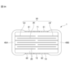
- FIG. 9 is a diagram showing the multilayer ceramic capacitor 1 of the second embodiment, and corresponds to FIG. 7.
- FIG. 10 is a diagram showing the multilayer ceramic capacitor 1 of the second embodiment, and is a diagram corresponding to the arrow diagram when looking at the second main surface TS2 side along the direction of the arrow X shown in FIG. be.
- the multilayer ceramic capacitor 1 according to the second embodiment includes the first main surface side hydrophobic section 71 and the second main surface side hydrophobic section 72 of the hydrophobic section 70 and the first main surface side hydrophilic section 81 and the second main surface side hydrophobic section 81 of the hydrophilic section 80.
- the aspect of the second main surface side hydrophilic portion 82 is different from the above embodiment.
- the hydrophobic portion 70 of the second embodiment will be explained.
- the first main surface side hydrophobic portion 71 is arranged to extend in the width direction W at the center of the laminate 10 in the length direction L. As shown in FIG. 9, the first main surface side hydrophobic portion 71 is arranged from the first side surface WS1 side to the second side surface WS2 side in the width direction W on the first main surface TS1.
- the first main surface side hydrophobic portion 71 has a first widthwise side surface portion 711 and a first widthwise center portion 712 .
- the first widthwise side surface portion 711 is located on the first side surface WS1 side and the second side surface WS2 side in the width direction W of the first main surface TS1. Specifically, the first widthwise side surface portion 711 is located at a portion of the first main surface TS1 that intersects with the first side surface WS1 and a portion that intersects with the second side surface WS2.
- the first widthwise center portion 712 is located on the center portion side of the first principal surface TS1 in the width direction W.
- the dimension d1 in the length direction L of the first main surface side hydrophobic portion 71 increases from the first widthwise side surface portion 711 toward the first widthwise center portion 712. That is, in the first main surface side hydrophobic portion 71, the dimension d1 in the length direction L is from the first side surface WS1 side or the second side surface WS2 side in the width direction W of the first main surface TS1 in the width direction W. It becomes larger toward the center.
- the second main surface side hydrophobic portion 72 is arranged so as to extend in the width direction W at the center of the laminate 10 in the length direction L. As shown in FIG. 10, the second main surface side hydrophobic portion 72 is arranged from the first side surface WS1 side to the second side surface WS2 side in the width direction W on the second main surface TS2.
- the second main surface side hydrophobic portion 72 has a second widthwise side surface portion 721 and a second widthwise center portion 722 .
- the second widthwise side surface portion 721 is located on the first side surface WS1 side and the second side surface WS2 side in the width direction W of the second main surface TS2. Specifically, the second widthwise side surface portion 721 is located at a portion of the second main surface TS2 that intersects with the first side surface WS1 and a portion that intersects with the second side surface WS2.
- the second widthwise center portion 722 is located on the center side in the width direction W of the second main surface TS2.
- the dimension d2 in the length direction L of the second main surface side hydrophobic portion 72 increases from the second widthwise side surface portion 721 toward the second widthwise center portion 722. That is, in the second main surface side hydrophobic portion 72, the dimension d2 in the length direction L is from the first side surface WS1 side or the second side surface WS2 side in the width direction W on the second main surface TS2. It becomes larger toward the center.
- the first side hydrophobic part 73 and the second side hydrophobic part 74 of this embodiment have the same configuration as the first embodiment, but the first main surface side hydrophobic part 71 and the second side hydrophobic part 74 of this embodiment have the same structure as the first embodiment.
- the structure may be similar to that of the main surface side hydrophobic portion 72 of No. 2.
- the first main surface side hydrophobic section 71 and the second main surface side hydrophobic section 72 of the hydrophobic section 70 of this embodiment are arranged continuously via the first side surface side hydrophobic section 73, and
- the two side hydrophobic portions 74 are arranged in succession.
- hydrophilic portion 80 of the second embodiment will be explained.
- Two hydrophilic parts 80 ie, hydrophilic parts 80a and 80b, are arranged on the surface of the laminate 10.
- the first main surface side hydrophilic section 81 of the hydrophilic section 80a is arranged between the first external electrode 40A and the hydrophobic section 70 on the first main surface TS1, as shown in FIG. Specifically, the first main surface side hydrophilic section 81 of the hydrophilic section 80a is arranged so as to cover the entire surface between the first external electrode 40A and the hydrophobic section 70 on the first main surface TS1. . Further, the first main surface side hydrophilic section 81 of the hydrophilic section 80b is arranged between the hydrophobic section 70 and the second external electrode 40B on the first main surface TS1.
- the first main surface side hydrophilic section 81 of the hydrophilic section 80b is arranged so as to cover the entire surface between the hydrophobic section 70 and the second external electrode 40B on the first main surface TS1. . That is, in the first main surface side hydrophilic portions 81 of the hydrophilic portions 80a and 80b, the dimension d3 in the length direction L is on the first side surface WS1 side or the second side surface WS2 in the width direction W of the first main surface TS1. It becomes smaller as it goes from the side toward the center in the width direction W.
- the second main surface side hydrophilic section 82 of the hydrophilic section 80a is arranged between the first external electrode 40A and the hydrophobic section 70 on the second main surface TS2, as shown in FIG. Specifically, the second main surface side hydrophilic section 82 of the hydrophilic section 80a is arranged so as to cover the entire surface between the first external electrode 40A and the hydrophobic section 70 on the second main surface TS2. . Further, the second main surface side hydrophilic section 82 of the hydrophilic section 80b is arranged between the hydrophobic section 70 and the second external electrode 40B on the second main surface TS2.
- the second main surface side hydrophilic section 82 of the hydrophilic section 80b is arranged to cover the entire surface between the hydrophobic section 70 and the second external electrode 40B on the second main surface TS2. . That is, the second main surface side hydrophilic portions 82 of the hydrophilic portions 80a and 80b have a dimension d4 in the length direction L on the first side surface WS1 side or the second side surface WS2 in the width direction W on the second main surface TS2. It becomes smaller as it goes from the side toward the center in the width direction W.
- the first side hydrophilic part 83 and the second side hydrophilic part 84 of this embodiment have the same configuration as the first embodiment, but the first main surface side hydrophilic part 81 and the second side hydrophilic part 84 of this embodiment have the same configuration as the first embodiment.
- the structure may be similar to that of the main surface side hydrophilic portion 82 of No. 2.
- the first main surface side hydrophilic section 81 and the second main surface side hydrophilic section 82 of the hydrophilic section 80 of this embodiment are arranged continuously via the first side surface side hydrophilic section 83, and
- the two side hydrophilic portions 84 are disposed in succession.
- the first main surface side hydrophobic portion 71 of the multilayer ceramic capacitor 1 according to the present embodiment is located on the first side surface WS1 side and the second side surface WS2 side in the width direction W of the first main surface TS1.
- the second main surface side hydrophobic portion 72 has a first width direction side surface portion 711 located on the center side in the width direction W, and a first width direction center portion 712 located on the center side in the width direction W.
- the dimension d1 in the length direction L of the first main surface side hydrophobic portion 71 increases from the first widthwise side surface portion 711 toward the first widthwise center portion 712
- the dimension d2 in the length direction L of the second main surface side hydrophobic portion 72 increases from the second widthwise side surface portion 721 toward the second widthwise center portion 722.
- the dimension d1 in the length direction L of the first main surface side hydrophobic part 71 and the dimension d2 in the length direction L of the second main surface side hydrophobic part 72 increase toward the center part side in the width direction W. Therefore, as shown in FIGS. 9 and 10, water droplets W generated due to dew condensation are guided to the hydrophilic portion 80 and easily removed from the surface of the laminate 10. Therefore, formation of a water droplet path spanning between the first external electrode 40A and the second external electrode 40B can be more effectively suppressed.
- FIG. 11 is a diagram showing a multilayer ceramic capacitor 1 according to the third embodiment, and corresponds to FIG. 7.
- the multilayer ceramic capacitor 1 according to the third embodiment differs from the first embodiment in the aspects of the hydrophobic portion 70 and the hydrophilic portion 80.
- a plurality of hydrophobic parts 70 in the third embodiment are arranged on the surface of the laminate 10. As shown in FIG. 11, between the first external electrode 40A and the second external electrode 40B on the surface of the laminate 10, there are three hydrophobic parts 70a, 70b, and 70c in the length direction. They are spaced apart from each other in L. Specifically, as shown in FIG. 11, the hydrophobic part 70a is arranged at the center in the length direction L, the hydrophobic part 70b is arranged between the first external electrode 40A and the hydrophobic part 70a, and the hydrophobic part 70a is arranged at the center in the length direction L. 70c is arranged between the hydrophobic portion 70a and the second external electrode 40B.
- Each hydrophobic portion 70 has a ring shape as a whole, and is arranged across the first main surface TS1, the second main surface TS2, the first side surface WS1, and the second side surface WS2 of the laminate 10.
- Each hydrophobic portion 70 includes a first main surface side hydrophobic portion 71 disposed on at least a portion of the first main surface TS1, and a second hydrophobic portion 71 disposed on at least a portion of the second main surface TS2.
- the first main surface side hydrophobic portion 71 of the hydrophobic portion 70a is arranged to extend in the width direction W in the width direction W at the center of the laminate 10 in the length direction L.
- the first main surface side hydrophobic portion 71 extends from an end on the first side surface WS1 side to an end on the second side surface WS2 side in the width direction W on the first main surface TS1.
- the second main surface side hydrophobic section 72, the first side surface side hydrophobic section 73, and the second side surface side hydrophobic section 74 of the hydrophobic section 70a are similar to the first main surface side hydrophobic section 71.
- the laminate 10 is arranged to extend in the width direction W in a strip-like manner in the center of the length direction L of the laminate 10 . Further, the first main surface side hydrophobic section 71 and the second main surface side hydrophobic section 72 of the hydrophobic section 70a are arranged continuously via the first side surface side hydrophobic section 73, and the second They are arranged continuously via the side hydrophobic portion 74 .
- the first main surface side hydrophobic section 71 of the hydrophobic section 70b extends in the width direction W between the first external electrode 40A and the first main surface side hydrophobic section 71 of the hydrophobic section 70a. It is arranged in a long and narrow strip.
- the first main surface side hydrophobic part 71 of the hydrophobic part 70b extends from the end on the first side surface WS1 side in the width direction W on the first main surface TS1 to the end on the second side surface WS2 side. It extends substantially parallel to the first main surface side hydrophobic portion 71 of the hydrophobic portion 70a.
- the first main surface side hydrophobic portion 71 of the hydrophobic portion 70b is arranged with an interval between the first external electrode 40A and the hydrophobic portion 70a.
- the second main surface side hydrophobic section 72, the first side surface side hydrophobic section 73, and the second side surface side hydrophobic section 74 of the hydrophobic section 70b are connected to the first external electrode 40A and the first side hydrophobic section 74 of the hydrophobic section 70a.
- the main surface side hydrophobic portion 71 of 1 is arranged so as to extend in the width direction W in a long and narrow strip shape.
- first main surface side hydrophobic section 71 and the second main surface side hydrophobic section 72 of the hydrophobic section 70b are arranged continuously via the first side surface side hydrophobic section 73, and the second They are arranged continuously via the side hydrophobic portion 74 .
- the first main surface side hydrophobic section 71 of the hydrophobic section 70c extends in the width direction W between the first main surface side hydrophobic section 71 of the hydrophobic section 70a and the second external electrode 40B. It is arranged in a long and narrow strip.
- the first main surface side hydrophobic part 71 of the hydrophobic part 70c extends from the end on the first side surface WS1 side in the width direction W on the first main surface TS1 to the end on the second side surface WS2 side. It extends substantially parallel to the first main surface side hydrophobic portion 71 of the hydrophobic portion 70c.
- the first main surface side hydrophobic portion 71 of the hydrophobic portion 70c is arranged with an interval between the hydrophobic portion 70c and the second external electrode 40B.
- the second main surface side hydrophobic section 72, the first side surface side hydrophobic section 73, and the second side surface side hydrophobic section 74 of the hydrophobic section 70c are the first main surface side hydrophobic section of the hydrophobic section 70a. 71 and the second external electrode 40B so as to extend in the width direction W into a long and narrow strip.
- first main surface side hydrophobic section 71 and the second main surface side hydrophobic section 72 of the hydrophobic section 70c are arranged continuously via the first side surface side hydrophobic section 73, and the second They are arranged continuously via the side hydrophobic portion 74 .
- a plurality of hydrophilic parts 80 in the third embodiment are arranged on the surface of the laminate 10. As shown in FIG. 11, between the first external electrode 40A and the second external electrode 40B on the surface of the laminate 10, there are four hydrophilic parts 80a, 80b, 80c, and 80d. They are arranged at intervals in the horizontal direction L. Specifically, as shown in FIG. 11, the hydrophilic part 80a is arranged between the first external electrode 40A and the hydrophobic part 70b, and the hydrophilic part 80b is arranged between the hydrophobic part 70b and the hydrophobic part 70a.
- the hydrophilic part 80c is arranged between the hydrophobic part 70a and the hydrophobic part 70c, and the hydrophilic part 80d is arranged between the hydrophobic part 70c and the second external electrode 40B. That is, the hydrophobic portion 70 is sandwiched between the hydrophilic portions 80 in the length direction L.
- Each hydrophilic portion 80 has a ring shape as a whole, and is arranged across the first main surface TS1, the second main surface TS2, the first side surface WS1, and the second side surface WS2 of the laminate 10.
- Each hydrophilic portion 80 includes a first main surface side hydrophilic portion 81 disposed on at least a portion of the first main surface TS1, and a second hydrophilic portion 81 disposed on at least a portion of the second main surface TS2.
- the first main surface side hydrophilic portion 81 of the hydrophilic portion 80a is arranged to extend in a strip-like shape in the width direction W between the first external electrode 40A and the hydrophobic portion 70b.
- the first main surface side hydrophilic section 81 of the hydrophilic section 80a is arranged to cover the entire surface between the first external electrode 40A and the hydrophobic section 70b on the first main surface TS1. . That is, the first main surface side hydrophilic section 81 of the hydrophilic section 80a is arranged so as to be in contact with the first main surface side hydrophobic section 71 of the hydrophobic section 70b.
- the first main surface side hydrophilic section 81 of the hydrophilic section 80a extends from the end on the first side surface WS1 side to the end on the second side surface WS2 side in the width direction W on the first main surface TS1.
- the second main surface side hydrophilic section 82, the first side surface side hydrophilic section 83, and the second side surface side hydrophilic section 84 of the hydrophilic section 80a are similar to the first main surface side hydrophilic section 81. It is arranged so as to cover the entire surface between the first external electrode 40A and the hydrophobic portion 70b.
- first main surface side hydrophilic section 81 and the second main surface side hydrophilic section 82 of the hydrophilic section 80a are arranged continuously via the first side surface side hydrophilic section 83, and the second They are arranged continuously via the side hydrophilic portion 84 .
- the first main surface side hydrophilic portion 81 of the hydrophilic portion 80b is arranged to extend in a strip-like shape in the width direction W between the hydrophobic portion 70b and the hydrophobic portion 70a.
- the first main surface side hydrophilic section 81 of the hydrophilic section 80b is arranged so as to cover the entire surface between the hydrophobic section 70b and the hydrophobic section 70a on the first main surface TS1. That is, the first main surface side hydrophilic section 81 of the hydrophilic section 80b is in contact with both the first main surface side hydrophobic section 71 of the hydrophobic section 70a and the first main surface side hydrophobic section 71 of the hydrophobic section 70b. Placed.
- the first main surface side hydrophilic section 81 of the hydrophilic section 80b extends from the end on the first side surface WS1 side to the end on the second side surface WS2 side in the width direction W on the first main surface TS1.
- the second main surface side hydrophilic section 82, the first side surface side hydrophilic section 83, and the second side surface side hydrophilic section 84 of the hydrophilic section 80b are similar to the first main surface side hydrophilic section 81. It is arranged so as to cover the entire surface between the hydrophobic part 70b and the hydrophobic part 70a.
- first main surface side hydrophilic section 81 and the second main surface side hydrophilic section 82 of the hydrophilic section 80b are arranged continuously via the first side surface side hydrophilic section 83, and the second They are arranged continuously via the side hydrophilic portion 84 .
- the first main surface side hydrophilic portion 81 of the hydrophilic portion 80c is arranged to extend in a strip-like shape in the width direction W between the hydrophobic portion 70a and the hydrophobic portion 70c.
- the first main surface side hydrophilic section 81 of the hydrophilic section 80c is arranged so as to cover the entire surface between the hydrophobic section 70a and the hydrophobic section 70c on the first main surface TS1. That is, the first main surface side hydrophilic section 81 of the hydrophilic section 80c is in contact with both the first main surface side hydrophobic section 71 of the hydrophobic section 70a and the first main surface side hydrophobic section 71 of the hydrophobic section 70c. Placed.
- the first main surface side hydrophilic section 81 of the hydrophilic section 80c extends from the end on the first side surface WS1 side to the end on the second side surface WS2 side in the width direction W on the first main surface TS1.
- the second main surface side hydrophilic section 82, the first side surface side hydrophilic section 83, and the second side surface side hydrophilic section 84 of the hydrophilic section 80c are similar to the first main surface side hydrophilic section 81. It is arranged so as to cover the entire surface between the hydrophobic part 70a and the hydrophobic part 70c.
- first main surface side hydrophilic section 81 and the second main surface side hydrophilic section 82 of the hydrophilic section 80c are arranged continuously via the first side surface side hydrophilic section 83, and the second They are arranged continuously via the side hydrophilic portion 84 .
- the first main surface side hydrophilic portion 81 of the hydrophilic portion 80d is arranged to extend in a strip-like manner in the width direction W between the hydrophobic portion 70c and the second external electrode 40B.
- the first main surface side hydrophilic section 81 of the hydrophilic section 80d is arranged to cover the entire surface between the hydrophobic section 70c and the second external electrode 40B on the first main surface TS1. . That is, the first main surface side hydrophilic section 81 of the hydrophilic section 80d is arranged so as to be in contact with the first main surface side hydrophobic section 71 of the hydrophobic section 70c.
- the first main surface side hydrophilic section 81 of the hydrophilic section 80d extends from the end on the first side surface WS1 side to the end on the second side surface WS2 side in the width direction W on the first main surface TS1.
- the second main surface side hydrophilic section 82, the first side surface side hydrophilic section 83, and the second side surface side hydrophilic section 84 of the hydrophilic section 80d are similar to the first main surface side hydrophilic section 81. It is arranged so as to cover the entire surface between the hydrophobic portion 70c and the second external electrode 40B.
- first main surface side hydrophilic section 81 and the second main surface side hydrophilic section 82 of the hydrophilic section 80d are arranged continuously via the first side surface side hydrophilic section 83, and the second They are arranged continuously via the side hydrophilic portion 84 .
- a plurality of hydrophobic parts 70 of the multilayer ceramic capacitor 1 according to the present embodiment are arranged.
- water droplets W generated due to dew condensation are guided to the hydrophilic part 80, and a water droplet path spanning the first external electrode 40A and the second external electrode 40B is formed. Formation can be more effectively suppressed.
- each of the plurality of hydrophobic parts 70 is sandwiched between the hydrophilic parts 80 in the length direction L, water droplets W are guided from each hydrophobic part 70 to the hydrophilic part 80 as shown in FIG. can be efficiently removed from
- FIG. 12 is a diagram showing the multilayer ceramic capacitor 1 of the fourth embodiment, and corresponds to FIG. 7.
- FIG. 13 is a hypothetical arrow view of the multilayer ceramic capacitor 1 along the virtual XIII direction shown in FIG. 2 is an arrow diagram when looking at the end surface LS2 of No. 2.
- FIG. 12 the outline of the laminate 10 covered with the hydrophobic part 70, the hydrophilic part 80, and the external electrode 40 is shown by a broken line. Further, in FIG. 13, the outline of the laminate 10 covered with the hydrophobic portion 70 is shown by a broken line.
- the multilayer ceramic capacitor 1 according to the fourth embodiment differs from the first embodiment in the aspects of the multilayer body 10 and the hydrophobic portion 70.
- the laminate 10 of this embodiment has a first main surface protrusion 91, a second main surface protrusion 92, a first side protrusion 93, and a second side protrusion on its surface. It differs from the laminate 10 of the first embodiment in that it has a portion 94 .
- the first main surface side convex portion 91 protrudes in the direction away from the laminate 10 at the center of the first main surface TS1 in the length direction L.
- the first main surface side convex portion 91 is formed so as to extend continuously in the width direction W.
- the first main surface side convex portion 91 is spaced apart from the first external electrode 40A and the second external electrode 40B.
- the first main surface side convex portion 91 is arranged from an end on the first side surface WS1 side to an end on the second side surface WS2 side in the width direction W on the first main surface TS1.
- the second main surface side convex portion 92 protrudes in the direction away from the laminate 10 at the center of the second main surface TS2 in the length direction L.
- the second main surface side convex portion 92 is formed so as to extend continuously in the width direction W.
- the second main surface side convex portion 92 is spaced apart from the first external electrode 40A and the second external electrode 40B.
- the second main surface side convex portion 92 is arranged from an end on the first side surface WS1 side to an end on the second side surface WS2 side in the width direction W on the first main surface TS1.
- the first side surface convex portion 93 protrudes in the direction away from the stacked body 10 at the center of the first side surface WS1 in the length direction L.
- the first side convex portion 93 is formed to extend continuously in the height direction T.
- the first side surface side convex portion 93 is arranged with an interval between the first external electrode 40A and the second external electrode 40B.
- the first side convex portion 93 is arranged from an end on the first main surface TS1 side to an end on the second main surface TS2 side in the height direction T on the first side surface WS1.
- the second side surface protrusion 94 protrudes in the direction away from the stacked body 10 at the center of the first side surface WS1 in the length direction L.
- the second side convex portion 94 is formed to extend continuously in the height direction T.
- the second side-side convex portion 94 is arranged at a distance from the first external electrode 40A and the second external electrode 40B.
- the second side convex portion 94 is arranged from the end on the first main surface TS1 side in the height direction T on the first side surface WS1 to the end on the second main surface TS2 side.
- the hydrophobic portion 70 of this embodiment includes a first main surface side hydrophobic portion 71, a second main surface side hydrophobic portion 72, a first side surface side hydrophobic portion 73, and a second side surface side hydrophobic portion 74. , has.
- the first main surface side hydrophobic portion 71 is arranged on the first main surface side convex portion 91. Specifically, the first main surface side hydrophobic portion 71 is arranged to cover the first main surface side convex portion 91. That is, the first main surface side hydrophobic portion 71 is arranged so as to extend in the width direction W at the center of the first main surface TS1 in the length direction L. The first main surface side hydrophobic portion 71 is arranged from an end on the first side surface WS1 side to an end on the second side surface WS2 side in the width direction W on the first main surface TS1.
- the second main surface side hydrophobic portion 72 is arranged on the second main surface side convex portion 92. Specifically, the second main surface side hydrophobic portion 72 is arranged so as to cover the second main surface side convex portion 92 . That is, the second main surface side hydrophobic portion 72 is arranged so as to extend in the width direction W at the center of the second main surface TS2 in the length direction L. The second main surface side hydrophobic portion 72 is arranged from an end on the first side surface WS1 side to an end on the second side surface WS2 side in the width direction W on the second main surface TS2.
- the first side-side hydrophobic portion 73 is arranged on the first side-side convex portion 93. Specifically, the first side surface hydrophobic portion 73 is arranged to cover the first side surface side convex portion 93 . That is, the first side surface hydrophobic portion 73 is arranged so as to extend in the height direction T at the center of the first side surface WS1 in the length direction L. The first side surface side hydrophobic portion 73 is arranged from an end on the first main surface TS1 side to an end on the second main surface TS2 side in the height direction T on the first side surface WS1.
- the second side-side hydrophobic portion 74 is arranged on the second side-side convex portion 94. Specifically, the second side surface hydrophobic portion 74 is arranged to cover the second side surface side convex portion 94 . That is, the second side surface hydrophobic portion 74 is arranged so as to extend in the height direction T at the center of the second side surface WS2 in the length direction L. The second side surface side hydrophobic portion 74 is arranged from an end on the first main surface TS1 side to an end on the second main surface TS2 side in the height direction T on the second side surface WS2.
- the hydrophobic portion 70 of this embodiment as shown in FIG. and are arranged continuously via the second side hydrophobic portion 74. That is, the hydrophobic portion 70 has a ring shape as a whole, and is arranged across the first main surface TS1, the second main surface TS2, the first side surface WS1, and the second side surface WS2 of the laminate 10.
- hydrophilic part 80 of this embodiment two hydrophilic parts 80a and 80b are arranged as in the first embodiment.
- the hydrophilic portion 80a is arranged to cover the entire surface between the first external electrode 40A and the hydrophobic portion 70.
- the hydrophilic portion 80b is arranged so as to cover the entire surface between the hydrophobic portion 70 and the second external electrode 40B. That is, the hydrophobic portion 70 is sandwiched between the hydrophilic portions 80 in the length direction L, and is in contact with both the hydrophilic portions 80a and 80b.
- the laminate 10 of the multilayer ceramic capacitor 1 has a first main surface that protrudes in a direction away from the surface of the laminate 10 at the center in the length direction L of the first main surface TS1.
- the first side convex portion 93 protrudes in the direction away from the surface of the laminate 10, and at the center in the length direction L of the second side WS2, the surface of the laminate 10
- a second side surface side convex portion 94 protrudes in a direction away from the first side surface side convex portion 93 .
- the first main surface side hydrophobic portion 71 is arranged on the first main surface side convex portion 91.
- the second main surface side hydrophobic portion 72 is disposed on the second main surface side convex portion 92
- the first side surface side hydrophobic portion 73 is disposed on the first side side convex portion 93
- the second main surface side hydrophobic portion 72 is arranged on the second main surface side convex portion 92
- the side surface side hydrophobic portion 74 is arranged on the second side surface side convex portion 94 .
- the present invention is not limited to the configuration of the above-described embodiments, and can be modified and applied as appropriate without changing the gist of the present invention. Note that the present invention also includes a combination of two or more of the individual desirable configurations described in the above embodiments.
- the multilayer ceramic capacitor 1 of the present invention can also be described as follows. ⁇ 1> It includes a plurality of laminated dielectric layers, and has a first main surface and a second main surface facing each other in the height direction, and a first side surface and a second main surface facing each other in the width direction perpendicular to the height direction.
- a laminate having a side surface, and a first end surface and a second end surface facing each other in a length direction perpendicular to the height direction and the width direction; a first internal electrode layer disposed on the plurality of dielectric layers and exposed on the first end surface; a second internal electrode layer disposed on the plurality of dielectric layers and exposed on the second end surface; a first external electrode disposed on the first end surface; A multilayer ceramic capacitor comprising a second external electrode disposed on the second end surface, A hydrophilic part and a hydrophobic part are arranged on the surface of the laminate,
- the hydrophilic part is a first main surface-side hydrophilic portion disposed on at least a portion of the first main surface and having a hydroxyl group; a second main surface-side hydrophilic portion disposed on at least a portion of the second main surface and having a hydroxyl group; a first side-side hydrophilic portion disposed on at least a portion of the first side surface and having a hydroxyl group; a second
- the first main surface side hydrophilic part and the second main surface side hydrophilic part are arranged in succession via the first side surface side hydrophilic part, and the second main surface side hydrophilic part arranged consecutively through
- the first main surface side hydrophobic portion and the second main surface side hydrophobic portion are disposed continuously via the first side surface side hydrophobic portion, and the second side surface side hydrophobic portion
- the multilayer ceramic capacitor according to ⁇ 1> which is arranged continuously through the multilayer ceramic capacitor.
- the first main surface side hydrophobic portion includes a first width side surface portion located on the first side surface side and the second side surface side in the width direction of the first main surface, and a first width side surface portion located on the first side surface side and the second side surface side in the width direction of the first main surface, a first widthwise center portion located on the center side of the
- the second main surface side hydrophobic portion includes a second width side surface portion located on the first side surface side and the second side surface side in the width direction of the second main surface; a second widthwise center portion located on the center side of the The lengthwise dimension of the first main surface side hydrophobic portion increases from the first widthwise side surface toward the first widthwise center, Any one of ⁇ 1> to ⁇ 3>, wherein the lengthwise dimension of the second main surface side hydrophobic portion increases from the second widthwise side surface portion toward the second widthwise center portion.
- ⁇ 5> The multilayer ceramic capacitor according to any one of ⁇ 1> to ⁇ 4>, wherein a plurality of the hydrophobic parts are arranged.
- the laminate includes: a first main surface side convex portion protruding in a direction away from the surface of the laminate at a central portion of the first main surface in the longitudinal direction; a second main surface side convex portion that projects in a direction away from the surface of the laminate at a central portion of the second main surface in the longitudinal direction; a first side convex portion protruding in a direction away from the surface of the laminate at a central portion of the first side in the longitudinal direction; a second side-side convex portion protruding in a direction away from the surface of the laminate at the center of the second side in the length direction;
- the first main surface side convex part and the second main side convex part are arranged continuously via the first side side convex part, and the second side side convex part arranged consecutively through
- the first main surface side hydrophobic portion is arranged on the first main surface side convex portion
- the second main surface side hydrophobic portion is arranged on the second main surface side convex portion, The
- Multilayer ceramic capacitor 10 Laminated body 11 Inner layer portion 12 First main surface side outer layer portion 13 Second main surface side outer layer portion 20 Dielectric layer 31 First internal electrode layer 32 Second internal electrode layer 40A First External electrode 40B Second external electrode 70, 70a, 70b, 70c Hydrophobic portion 71 First main surface side hydrophobic portion 72 Second main surface side hydrophobic portion 73 First side surface side hydrophobic portion 74 Second side side hydrophobic portion Parts 80, 80a, 80b, 80c, 80d Hydrophilic portion 81 First main surface hydrophilic portion 82 Second main surface hydrophilic portion 83 First side hydrophilic portion 84 Second side hydrophilic portion L Length direction LS1 First end surface LS2 Second end surface T Lamination direction TS1 First main surface TS2 Second main surface W Width direction WS1 First side surface WS2 Second side surface
Landscapes
- Engineering & Computer Science (AREA)
- Power Engineering (AREA)
- Manufacturing & Machinery (AREA)
- Microelectronics & Electronic Packaging (AREA)
- Chemical & Material Sciences (AREA)
- Ceramic Engineering (AREA)
- Inorganic Chemistry (AREA)
- Fixed Capacitors And Capacitor Manufacturing Machines (AREA)
- Ceramic Capacitors (AREA)
Priority Applications (5)
| Application Number | Priority Date | Filing Date | Title |
|---|---|---|---|
| JP2024536878A JP7790575B2 (ja) | 2022-07-27 | 2023-06-29 | 積層セラミックコンデンサ |
| KR1020247039537A KR102856999B1 (ko) | 2022-07-27 | 2023-06-29 | 적층 세라믹 콘덴서 |
| EP23846115.6A EP4564387A1 (en) | 2022-07-27 | 2023-06-29 | Multilayer ceramic capacitor |
| CN202380041219.3A CN119156682A (zh) | 2022-07-27 | 2023-06-29 | 层叠陶瓷电容器 |
| US18/925,472 US20250054695A1 (en) | 2022-07-27 | 2024-10-24 | Multilayer ceramic capacitor |
Applications Claiming Priority (2)
| Application Number | Priority Date | Filing Date | Title |
|---|---|---|---|
| JP2022-119349 | 2022-07-27 | ||
| JP2022119349 | 2022-07-27 |
Related Child Applications (1)
| Application Number | Title | Priority Date | Filing Date |
|---|---|---|---|
| US18/925,472 Continuation US20250054695A1 (en) | 2022-07-27 | 2024-10-24 | Multilayer ceramic capacitor |
Publications (1)
| Publication Number | Publication Date |
|---|---|
| WO2024024382A1 true WO2024024382A1 (ja) | 2024-02-01 |
Family
ID=89705997
Family Applications (1)
| Application Number | Title | Priority Date | Filing Date |
|---|---|---|---|
| PCT/JP2023/024153 Ceased WO2024024382A1 (ja) | 2022-07-27 | 2023-06-29 | 積層セラミックコンデンサ |
Country Status (6)
| Country | Link |
|---|---|
| US (1) | US20250054695A1 (https=) |
| EP (1) | EP4564387A1 (https=) |
| JP (1) | JP7790575B2 (https=) |
| KR (1) | KR102856999B1 (https=) |
| CN (1) | CN119156682A (https=) |
| WO (1) | WO2024024382A1 (https=) |
Citations (4)
| Publication number | Priority date | Publication date | Assignee | Title |
|---|---|---|---|---|
| WO2002082480A1 (en) | 2001-04-05 | 2002-10-17 | Matsushita Electric Industrial Co., Ltd. | Ceramic electronic device and method of manufacture thereof |
| JP2014110318A (ja) * | 2012-12-03 | 2014-06-12 | Murata Mfg Co Ltd | 電子部品 |
| JP2015198235A (ja) * | 2014-04-03 | 2015-11-09 | 株式会社村田製作所 | 電子部品及びその製造方法 |
| JP2020167379A (ja) * | 2019-03-28 | 2020-10-08 | 太陽誘電株式会社 | 積層セラミックコンデンサおよびその製造方法 |
-
2023
- 2023-06-29 WO PCT/JP2023/024153 patent/WO2024024382A1/ja not_active Ceased
- 2023-06-29 KR KR1020247039537A patent/KR102856999B1/ko active Active
- 2023-06-29 JP JP2024536878A patent/JP7790575B2/ja active Active
- 2023-06-29 EP EP23846115.6A patent/EP4564387A1/en active Pending
- 2023-06-29 CN CN202380041219.3A patent/CN119156682A/zh active Pending
-
2024
- 2024-10-24 US US18/925,472 patent/US20250054695A1/en active Pending
Patent Citations (4)
| Publication number | Priority date | Publication date | Assignee | Title |
|---|---|---|---|---|
| WO2002082480A1 (en) | 2001-04-05 | 2002-10-17 | Matsushita Electric Industrial Co., Ltd. | Ceramic electronic device and method of manufacture thereof |
| JP2014110318A (ja) * | 2012-12-03 | 2014-06-12 | Murata Mfg Co Ltd | 電子部品 |
| JP2015198235A (ja) * | 2014-04-03 | 2015-11-09 | 株式会社村田製作所 | 電子部品及びその製造方法 |
| JP2020167379A (ja) * | 2019-03-28 | 2020-10-08 | 太陽誘電株式会社 | 積層セラミックコンデンサおよびその製造方法 |
Also Published As
| Publication number | Publication date |
|---|---|
| KR20250002678A (ko) | 2025-01-07 |
| EP4564387A1 (en) | 2025-06-04 |
| CN119156682A (zh) | 2024-12-17 |
| US20250054695A1 (en) | 2025-02-13 |
| KR102856999B1 (ko) | 2025-09-08 |
| JPWO2024024382A1 (https=) | 2024-02-01 |
| JP7790575B2 (ja) | 2025-12-23 |
Similar Documents
| Publication | Publication Date | Title |
|---|---|---|
| KR102926218B1 (ko) | 적층 세라믹 콘덴서 | |
| JP7655713B2 (ja) | 積層セラミックコンデンサ | |
| US11183334B2 (en) | Multilayer ceramic electronic component | |
| US12249465B2 (en) | Multilayer ceramic capacitor | |
| JP7790575B2 (ja) | 積層セラミックコンデンサ | |
| JP2021125673A (ja) | 積層セラミックコンデンサ | |
| JP2023172524A (ja) | 積層セラミックコンデンサ | |
| JP7751261B2 (ja) | 積層セラミックコンデンサ | |
| JP7736197B2 (ja) | 積層セラミックコンデンサ | |
| US12505955B2 (en) | Multilayer ceramic electronic component | |
| US20250157744A1 (en) | Multilayer ceramic electronic component and mounting structure of multilayer ceramic electronic component | |
| US20260011493A1 (en) | Multilayer ceramic capacitor | |
| US20240312709A1 (en) | Multilayer ceramic capacitor and multilayer ceramic capacitor-mounted structure | |
| WO2026069543A1 (ja) | 積層セラミック電子部品 | |
| JP2025147712A (ja) | 積層セラミックコンデンサ | |
| KR20260012837A (ko) | 적층 세라믹 콘덴서 | |
| CN119365951A (zh) | 层叠陶瓷电容器以及层叠陶瓷电容器的制造方法 | |
| WO2024004304A1 (ja) | 貫通型積層セラミックコンデンサ | |
| JP2024162476A (ja) | 積層セラミックコンデンサ | |
| WO2026063169A1 (ja) | 積層セラミックコンデンサ | |
| KR20250141055A (ko) | 적층 세라믹 콘덴서 | |
| WO2026063471A1 (ja) | 積層セラミック電子部品 | |
| WO2025126319A1 (ja) | 積層セラミック電子部品 | |
| KR20250136405A (ko) | 적층 세라믹 콘덴서 | |
| WO2024257450A1 (ja) | 積層セラミック部品 |
Legal Events
| Date | Code | Title | Description |
|---|---|---|---|
| 121 | Ep: the epo has been informed by wipo that ep was designated in this application |
Ref document number: 23846115 Country of ref document: EP Kind code of ref document: A1 |
|
| WWE | Wipo information: entry into national phase |
Ref document number: 202417082437 Country of ref document: IN |
|
| WWE | Wipo information: entry into national phase |
Ref document number: 202380041219.3 Country of ref document: CN |
|
| ENP | Entry into the national phase |
Ref document number: 20247039537 Country of ref document: KR Kind code of ref document: A |
|
| WWE | Wipo information: entry into national phase |
Ref document number: 1020247039537 Country of ref document: KR |
|
| WWE | Wipo information: entry into national phase |
Ref document number: 2024536878 Country of ref document: JP |
|
| WWE | Wipo information: entry into national phase |
Ref document number: 2023846115 Country of ref document: EP |
|
| NENP | Non-entry into the national phase |
Ref country code: DE |
|
| ENP | Entry into the national phase |
Ref document number: 2023846115 Country of ref document: EP Effective date: 20250227 |
|
| WWP | Wipo information: published in national office |
Ref document number: 2023846115 Country of ref document: EP |