WO2024019142A1 - 弾性波装置、通信装置、および製造方法 - Google Patents
弾性波装置、通信装置、および製造方法 Download PDFInfo
- Publication number
- WO2024019142A1 WO2024019142A1 PCT/JP2023/026753 JP2023026753W WO2024019142A1 WO 2024019142 A1 WO2024019142 A1 WO 2024019142A1 JP 2023026753 W JP2023026753 W JP 2023026753W WO 2024019142 A1 WO2024019142 A1 WO 2024019142A1
- Authority
- WO
- WIPO (PCT)
- Prior art keywords
- piezoelectric layer
- electrode
- wave device
- elastic wave
- acoustic wave
- Prior art date
- Legal status (The legal status is an assumption and is not a legal conclusion. Google has not performed a legal analysis and makes no representation as to the accuracy of the status listed.)
- Ceased
Links
Images



Classifications
-
- H—ELECTRICITY
- H03—ELECTRONIC CIRCUITRY
- H03H—IMPEDANCE NETWORKS, e.g. RESONANT CIRCUITS; RESONATORS
- H03H3/00—Apparatus or processes specially adapted for the manufacture of impedance networks, resonating circuits, resonators
- H03H3/007—Apparatus or processes specially adapted for the manufacture of impedance networks, resonating circuits, resonators for the manufacture of electromechanical resonators or networks
- H03H3/08—Apparatus or processes specially adapted for the manufacture of impedance networks, resonating circuits, resonators for the manufacture of electromechanical resonators or networks for the manufacture of resonators or networks using surface acoustic waves
-
- H—ELECTRICITY
- H03—ELECTRONIC CIRCUITRY
- H03H—IMPEDANCE NETWORKS, e.g. RESONANT CIRCUITS; RESONATORS
- H03H9/00—Networks comprising electromechanical or electro-acoustic elements; Electromechanical resonators
- H03H9/02—Details
- H03H9/125—Driving means, e.g. electrodes, coils
- H03H9/145—Driving means, e.g. electrodes, coils for networks using surface acoustic waves
Definitions
- the present disclosure relates to an elastic wave device.
- an IDT electrode is formed of an aluminum film on a piezoelectric substrate.
- the invention includes a piezoelectric layer, an electrode provided on the piezoelectric layer, and a cover portion that covers at least a portion of a side surface of the electrode, and the cover portion includes: Contains elements other than oxygen and nitrogen that constitute the piezoelectric layer.
- the steps include forming a piezoelectric layer, forming an electrode provided on the piezoelectric layer, and dry etching the piezoelectric layer and the electrode. ,including.
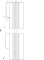
- FIG. 1 is a schematic diagram showing a cross-sectional structure of an elastic wave device according to Embodiment 1.
- FIG. FIG. 3 is a diagram comparing elastic wave devices according to a comparative example and a first embodiment side by side.
- FIG. 2 is a diagram in which a protective film is formed on the elastic wave device shown in FIG. 1; 1 is an example showing a cross-sectional structure of an elastic wave device according to Embodiment 1.
- FIG. This is an enlarged photograph of a part of FIG. 4.
- 6 is a graph showing the composition amount of tantalum on a specific line segment in FIG. 5.
- FIG. These are the results of comparing the power resistance with and without dry etching.
- FIG. 3 is a diagram comparing elastic wave devices according to a comparative example and a first embodiment side by side.
- FIG. 2 is a diagram in which a protective film is formed on the elastic wave device shown in FIG. 1
- 1 is an example showing a cross-sectional structure of an elastic wave device according
- FIG. 3 is a schematic diagram showing a cross-sectional structure of an elastic wave device according to a second embodiment.
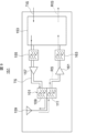
- 12 is a diagram illustrating a schematic configuration of a communication device in Embodiment 3.
- FIG. FIG. 2 is a schematic diagram showing a cross-sectional structure of an elastic wave device.
- the elastic wave device excites plate waves, for example.
- the elastic wave device may excite bulk waves.
- Plate waves are classified into Lamb waves whose vibration planes are perpendicular to the plate surface, and SH waves whose vibration planes are parallel to the plate surface.
- Lamb waves are classified into S mode, which is a symmetric mode, and A mode, which is an antisymmetric mode.
- the A1 mode corresponds to a first-order antisymmetric mode.
- an elastic wave device using an A1 mode ram wave will be described, but the present invention is not limited thereto.
- it may be an elastic wave device using bulk waves in thickness shear mode.
- plate waves have a large change in resonance characteristics when the thickness of the piezoelectric layer 3, which will be described later, changes.
- the bulk wave also has a large change in resonance characteristics when the thickness of the piezoelectric layer 3, which will be described later, changes.
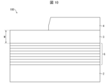
- FIG. 9 is a schematic diagram showing a cross-sectional structure of the elastic wave device 100.
- the acoustic wave device 100 is configured by stacking a support substrate 2, a multilayer film 6, a piezoelectric layer 3, and an electrode 4 in this order.
- the support substrate 2 is a substrate that supports the piezoelectric layer 3 and the electrodes 4.
- the support substrate 2 may be made of silicon, or may be made of various materials such as sapphire or glass.
- the multilayer film 6 is an acoustic reflection film in which a large number of low acoustic impedance layers 6a and high acoustic impedance layers 6b are alternately laminated.
- four low acoustic impedance layers 6a and four high acoustic impedance layers 6b are alternately stacked. That is, the multilayer film 6 reflects the Lamb waves propagating from above the acoustic wave device 100 at the interface between the low acoustic impedance layer 6a and the high acoustic impedance layer 6b.
- the low acoustic impedance layer 6a may contain SiO2.
- the high acoustic impedance layer 6b may contain at least one of HfO 2 , Ta 2 O 5 , and ZrO 2 , and is, for example, HfO 2 .
- the multilayer film 6 may be omitted.
- the piezoelectric layer 3 is formed relatively thin.
- the thickness W of the piezoelectric layer 3 may be one wavelength or less of the plate wave excited by the electrode 4, which is determined by the pitch of the electrode 4, which will be described later.
- the piezoelectric layer 3 is made of lithium tantalate, lithium niobate, or crystal. Further, the piezoelectric layer 3 is not limited to these materials, and various piezoelectric materials may be used. In the following description, the piezoelectric layer 3 will be described as lithium tantalate.
- the electrode 4 is a comb-shaped IDT (interdigital transducer) electrode, that is, a large number of electrode fingers are formed. Further, in the portion where the electrode 4 is not formed, the piezoelectric layer 3 is exposed. The wavelength of the plate wave excited by the piezoelectric layer 3 is determined by the pitch of the IDT electrodes.
- the electrode 4 is made of aluminum, copper, or an alloy thereof.
- the piezoelectric layer 3 is configured so that plate waves are excited in the piezoelectric layer 3 by applying an alternating current to the electrode 4.
- the thickness of the piezoelectric layer 3 and/or the electrode 4 differs depending on the position of the support substrate 2.
- the support substrate 2 is, for example, a silicon wafer. Therefore, the elastic wave device 100 has different frequency characteristics depending on the position of the support substrate 2.
- the thicknesses of the piezoelectric layer 3 and the electrodes 4 can be adjusted by etching or the like.
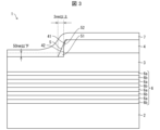
- FIG. 1 is a schematic diagram showing a cross-sectional structure of an elastic wave device 1 according to the first embodiment.
- FIG. 2 is a diagram comparing the elastic wave devices 100 and 1 according to the comparative example and the first embodiment side by side.
- FIG. 3 is an example showing a cross-sectional structure of the elastic wave device 1 according to the first embodiment.
- SEM scanning electron microscope
- the area where the surface of the piezoelectric layer 3 is exposed is thinner, and the difference in thickness is 50 nm. It is as follows. That is, the thickness of the region of the electrode 4 in the piezoelectric layer 3 is larger than the thickness of the region of the piezoelectric layer 3 whose surface is exposed, and the thickness of the region of the electrode 4 and the surface of the piezoelectric layer 3 are The difference in thickness between the exposed region and the exposed region is 50 nm or less.
- the edges of the electrodes 4 were scraped by the dry etching, and it can be seen that they were beveled at 43. This provides the effect of reducing stress migration due to vibration of the electrode 4.
- the elastic wave device 1 is provided with a cover portion 5 that covers at least a portion of the side surface of the electrode 4.
- This cover part 5 is a part that does not exist in the elastic wave device 100.
- the support substrate 2 supports the piezoelectric layer 3, the electrode 4, and the cover part 5.
- the thickness of the thickest part of the cover part 5 is 3 nm or more.
- the cover portion 5 includes a first portion 51 and a second portion that is located above the electrode 4 than the first portion 51 and is thinner than the first portion. That is, the cover part 5 does not have a uniform thickness, but the first part 51 and the second part 52 have different thicknesses. Further, the electrode 4 may become thinner as it goes upward.
- the side surface of the electrode 4 has a first surface 41 that is non-perpendicular to the surface of the piezoelectric layer 3.
- the first surface is located above the electrode 4.
- the cover portion 5 is also in contact with the first surface.
- the side surface of the electrode 4 has a second surface 42 near the surface of the piezoelectric layer 3 that is more perpendicular to the surface of the piezoelectric layer 3 than the first surface 41 .
- the first surface and the second surface are continuous.
- the cover portion is also in contact with the second surface 42 .
- the first surface 41 includes the second portion 52
- the second surface 42 includes the first portion 51. That is, the angle between the second surface 42 and the direction perpendicular to the surface of the piezoelectric layer 3 is smaller than the angle between the first surface 41 and the direction perpendicular to the surface of the piezoelectric layer 3 . Therefore, in the second surface 42, the thickness of the cover portion 5 tends to increase.
- the contact area between the electrode 4 and the cover part 5 is increased. This can reduce the formation of hillocks (protrusions) on the surface of the electrode 4, and has the effect of improving power durability against electromigration.
- the second surface 42 is close to perpendicular to the surface of the piezoelectric layer 3, the amount of the cover portion 5 deposited becomes large. Therefore, when a protective film is created to cover the piezoelectric layer 3 and the electrode 4, the coverage of the protective film in the vicinity of the second surface 42 is improved, and the effect of reducing electrolytic corrosion can be obtained.
- FIG. 3 is a diagram in which a protective film 7 is formed on the acoustic wave device 1 shown in FIG. 1.
- the protective film 7 covers the piezoelectric layer 3 and at least a portion of the electrode 4. Specifically, the protective film 7 covers the lower side of the electrode 4 , that is, the portion of the electrode 4 close to the piezoelectric layer 3 via the first portion 51 .
- the protective film 7 can be made of various materials such as SiO 2 , SiN, SiON, AlN, ZrO 2 , Ta 2 O 5 , ZnO, Al 2 O 3 , and HfO 2 , for example, SiO 2 , SiN, AlN, Ta. 2 O 5 etc.
- composition of cover part 5 As shown in FIG. 3, in the SEM image, it is highly likely that the compositions of the piezoelectric layer 3 and the cover portion 5 are similar. This is considered to be due to the redeposition of the portion removed by dry etching. That is, it is considered that the electrode 4 was covered by the cover part 5.
- FIG. 4 is an enlarged view of a part (reference numeral 8) of the photograph in FIG. 3. Further, FIG. 5 shows the measurement of the composition amount of tantalum on the line segment indicated by reference numeral 9 in FIG.
- the measured value increases in the amount of tantalum between 60 nm and 80 nm. That is, it can be seen that tantalum element is contained in this section of the cover portion 5. In fact, in this section and the corresponding upper part of FIG. 5, the shading changes and the composition probably changes, so it is thought that tantalum element is being measured.
- the electrode 4 was covered due to the composition of the piezoelectric layer 3.
- the element constituting the cover portion 5 may include lithium or tantalum.
- the element constituting the cover portion 5 may include lithium or niobium.
- the piezoelectric layer 3 is made of crystal, the element constituting the cover portion 5 may include silicon.
- the cover portion 5 may contain various elements contained in the piezoelectric material. The various elements are, for example, metal elements. That is, the cover portion 5 contains elements constituting the piezoelectric layer 3 other than oxygen and nitrogen. This description suffices if the cover part 5 contains an element other than oxygen and nitrogen among the elements constituting the piezoelectric layer 3, and denies that the cover part 5 contains oxygen and nitrogen. isn't it.
- the cover portion 5 may be made of lithium tantalate, that is, tantalum oxide.
- the cover portion 5 may be made of lithium niobate, that is, niobium oxide.
- FIG. 6 shows the results of comparing the power durability with and without dry etching. That is, when dry etching was performed, the elastic wave device 1 was tested, and when dry etching was not performed, the elastic wave device 100 was tested. Further, two types of tests were conducted: measuring the breakdown power of the element of the elastic wave device 1 or 100, and measuring the migration power at which electromigration begins to occur at the electrode 4.
- the electrode 4 is covered by the cover portion 5, the insulation distance is increased. Furthermore, since the electrode 4 is covered by the cover part 5, the possibility of hillock formation is reduced.
- the amount of deposition on the cover portion 5 or the area in contact with the cover portion 5 can be increased by the difference in the inclination angles of the first surface 41 and the second surface 42 with respect to the piezoelectric layer 3. As a result, electromigration becomes difficult to occur.
- the elastic wave device 1 is manufactured in the following steps. First, the piezoelectric layer 3 is formed on the support substrate 2. Furthermore, an aluminum film is formed on the piezoelectric layer 3, and the electrode 4 is formed by etching the aluminum film using a photoresist mask.
- the thicknesses of the piezoelectric layer 3 and the electrodes 4 are measured using various thickness measurement methods. This is to calculate how much etching should be done in order to obtain the elastic wave device 1 whose frequency characteristics are adjusted to a desired value.
- the amount of etching to achieve the desired frequency characteristics is determined, and the piezoelectric layer 3 and electrodes 4 are dry-etched using different amounts of etching for each element to obtain the acoustic wave device 1.
- the cover portion 5 is formed by attaching the material separated from the piezoelectric layer 3 by dry etching to at least a portion of the side surface of the electrode 4.
- the thickness of the piezoelectric layer 3 can be adjusted to obtain desired frequency characteristics, and at the same time, the cover portion 5 that improves the power resistance can be formed. Therefore, since it is a process for obtaining desired frequency characteristics, it is the minimum necessary process from the beginning, and there is no need to add multiple processes to the manufacturing process.
- FIG. 7 is a schematic diagram showing a cross-sectional structure of an elastic wave device 1a according to the second embodiment.
- the elastic wave device 1 a is different from the elastic wave device 1 in that a portion of the electrode 4 is embedded in the piezoelectric layer 3 . Thereafter, dry etching is performed in the same manner as in Embodiment 1, and as a result, the cover portion 5 is formed.
- the electrode 4 is covered by the piezoelectric layer 3 in the embedded part, that is, the electrode 4 is covered by an element having a higher density than aluminum, such as tantalum or niobium. ing. As a result, electromigration is less likely to occur in the electrode 4, and the power resistance is improved.
- FIG. 8 is a diagram illustrating a schematic configuration of the communication device 151 in the third embodiment.
- the communication device 151 is an application example of an elastic wave device according to one aspect of the present disclosure, and performs wireless communication using radio waves.
- the communication device 151 may include one duplexer 101 as a transmission filter 109 and another duplexer 101 as a reception filter 111.
- Each of the two duplexers 101 may include an elastic wave device according to one aspect of the present disclosure.
- the elastic wave device may be the elastic wave device 1 or the elastic wave device 1a. In this way, the communication device 151 may include an elastic wave device according to one aspect of the present disclosure.
- a transmission information signal TIS containing information to be transmitted may be modulated and frequency increased by an RF-IC (Radio Frequency-Integrated Circuit) 153, and converted into a transmission signal TS. Modulation and frequency raising may be a conversion to a high frequency signal with a carrier frequency.
- the bandpass filter 155 may remove unnecessary components other than the transmission passband for the TS.
- the TS after removing unnecessary components may be amplified by the amplifier 157 and input to the transmission filter 109.
- the transmission filter 109 may remove unnecessary components outside the transmission passband from the input transmission signal TS.
- the transmission filter 109 may output the TS from which unnecessary components have been removed to the antenna 159 via the antenna terminal.
- the antenna terminal may be, for example, the above-mentioned TCin.
- the antenna 159 may convert the TS, which is an electrical signal input to itself, into a radio wave as a wireless signal, and transmit the radio wave to the outside of the communication device 151.
- the antenna 159 may convert the received radio waves from the outside into a reception signal RS, which is an electrical signal, and input the RS to the reception filter 111 via the antenna terminal.
- the reception filter 111 may remove unnecessary components other than the reception passband from the input RS.
- the reception filter 111 may output the reception signal RS from which unnecessary components have been removed to the amplifier 161.
- the output RS may be amplified by the amplifier 161.
- the bandpass filter 163 may remove unnecessary components other than the receiving passband from the amplified RS.
- the frequency of the RS after unnecessary component removal is lowered and demodulated by the RF-IC 153, and may be converted into a received information signal RIS.
- the TIS and RIS may be low frequency signals (baseband signals) containing appropriate information.
- TIS and RIS may be analog audio signals or digitized audio signals.
- the passband of the wireless signal may be set as appropriate and may conform to various known standards.
- An acoustic wave device includes a piezoelectric layer, an electrode provided on the piezoelectric layer, and a piezoelectric layer that covers at least a part of a side surface of the electrode, and the piezoelectric layer other than oxygen and nitrogen. and a cover portion containing elements constituting the.
- the fear of electromigration of the electrode can be reduced by the cover part, and the power resistance of the acoustic wave device is improved.
- the piezoelectric layer may include lithium tantalate, and the element may be lithium or tantalum.
- the piezoelectric layer may include lithium niobate, and the element may be lithium or niobium.
- the piezoelectric layer may include crystal, and the element may be silicon.
- the cover portion includes a part of the elements that constitute the piezoelectric layer. Therefore, the constituent elements of the piezoelectric layer redeposited by dry etching cover the electrodes.
- the piezoelectric layer may be made of lithium tantalate, and the cover portion may contain tantalum oxide.
- the piezoelectric layer may be made of lithium niobate, and the cover portion may contain niobium oxide.
- the cover portion includes a compound of the elements that constitute the piezoelectric layer. Therefore, the compound related to the piezoelectric layer redeposited by dry etching covers the electrode.
- the density of the cover portion may be greater than the density of the electrode.
- electromigration of the electrode can be prevented by covering the electrode with the cover portion made of an element with higher density than the electrode.
- the thickness of the thickest portion of the cover portion may be 3 nm or more.
- the cover portion can be made to have a thickness of 3 nm or more, and the electrode can be covered with a sufficient thickness of the cover portion. Therefore, the power resistance of the elastic wave device can be improved.
- the cover portion includes a first portion and is located above the electrode than the first portion, and and a second portion thinner than the first portion.
- the cover portion can be made thicker toward the piezoelectric layer side.
- An acoustic wave device in any one of aspects 1 to 9, includes a protective film that covers at least a portion of the piezoelectric layer and the electrode, and the protective film includes a protective film that covers at least a portion of the piezoelectric layer and the electrode. A portion of the electrode close to the piezoelectric layer may be covered through one portion.
- the coverage of the protective film near the lower side of the electrode is improved, and the effect of reducing electrolytic corrosion can be obtained.
- the side surface of the electrode has a first surface that is non-perpendicular to the surface of the piezoelectric layer.
- the cover portion may be in contact with the first surface.
- the side surface of the electrode can have a first surface that is non-perpendicular to the surface of the piezoelectric layer. Therefore, the contact area between the electrode and the cover part can be increased.
- the side surface of the electrode further includes a second surface that is located near the surface of the piezoelectric layer and is continuous with the first surface. , an angle between a direction perpendicular to the surface of the piezoelectric layer and the second surface is smaller than an angle between the perpendicular direction and the first surface, and the cover portion is on the second surface. You can touch it.
- the side surface of the electrode can have a second surface that is closer to perpendicular than the first surface near the surface of the piezoelectric layer. Therefore, the amount of deposition on the cover portion can be increased on the second surface.
- the thickness of the region of the electrode in the piezoelectric layer is the thickness of the region of the piezoelectric layer whose surface is exposed. It may be larger.
- the thickness of the piezoelectric layer can be made thinner in the region where the surface of the piezoelectric layer is exposed than in the region where the electrodes overlap. That is, the piezoelectric layer can also be dry-etched together with the electrodes, making processing easy.
- the difference between the thickness of the region of the electrode and the thickness of the region where the surface of the piezoelectric layer is exposed is: It may be 50 nm or less.
- the difference between the thickness of the piezoelectric layer in the region where the electrodes overlap and the thickness of the piezoelectric layer in the region where the surface of the piezoelectric layer is exposed can be 50 nm or less.
- An acoustic wave device in any one of the aspects 1 to 14, further includes a support substrate that supports the piezoelectric layer, the electrode, and the cover part, and the electrode is an electrode.
- the piezoelectric layer may be a finger, and the thickness of the piezoelectric layer may be one wavelength or less determined by the pitch of the electrode fingers, and the piezoelectric layer may be configured to excite plate waves.
- the elastic wave device can be configured to function as an elastic wave device.
- the elastic wave device according to aspect 16 of the present disclosure may excite waves in any one of aspects 1 to 14 above.
- the elastic wave device according to aspect 17 of the present disclosure may excite bulk waves in any one of aspects 1 to 14 above.
- a communication device may include the elastic wave device according to any one of aspects 1 to 17.
- a manufacturing method includes a step of forming a piezoelectric layer, a step of forming an electrode on the piezoelectric layer, and dry etching the piezoelectric layer and the electrode. and attaching the material separated from the piezoelectric layer to at least a portion of the side surface of the electrode.
Landscapes
- Physics & Mathematics (AREA)
- Acoustics & Sound (AREA)
- Engineering & Computer Science (AREA)
- Manufacturing & Machinery (AREA)
- Surface Acoustic Wave Elements And Circuit Networks Thereof (AREA)
Abstract
Description
(板波)
弾性波装置は、例えば、板波を励振する。または、弾性波装置は、バルク波を励振してもよい。板波は、その振動面が板表面に対して垂直であるラム波と、その振動面が板表面に対して平行であるSH波と、に分類される。ラム波は、対称モードであるSモードと、反対称モードであるAモードと、に分類される。A1モードは、1次の反対称モードに該当する。本実施形態では、A1モードラム波を用いた弾性波装置に関して記載するが、これに限定されない。例えば、厚み滑りモードのバルク波を用いた弾性波装置であってもよい。板波は、種々の波の中で、後述する圧電体層3の厚みが変化する場合、共振特性の変化が大きい。バルク波もまた、後述する圧電体層3の厚みが変化する場合、共振特性の変化が大きい。
比較例に係る弾性波装置100では、図9に示すように、圧電体層3の表面と、圧電体層3および電極4の界面と、はほぼ一致する。すなわち、圧電体層3の上に、電極4が形成され、その後、エッチング等は行われていない。
比較例の弾性波装置100では、支持基板2の位置に応じて、圧電体層3および/または電極4の厚みが異なっている。支持基板2は、例えばシリコンウエハである。そのため、弾性波装置100は、支持基板2の位置に応じて周波数特性が異なってくる。
実施形態1に係る弾性波装置1では、事前に計測した厚みを基にして、各弾性波装置の素子ごと、または素子の部分ごとに、異なる厚みでドライエッチングする。図1は、実施形態1に係る弾性波装置1の断面構造を示す模式図である。また、図2は、比較例と実施形態1とに係る弾性波装置100および1を並べて比較した図である。
また、弾性波装置1は、電極4の側面の少なくとも一部を覆うカバー部5が形成されている。このカバー部5は、弾性波装置100には存在しない部分である。ここで、支持基板2は、圧電体層3、電極4およびカバー部5を支持する。
図3に示すようにSEM画像において、圧電体層3とカバー部5との組成が類似している可能性が高い。これは、ドライエッチングによって削られた部分がリデポジションしたと考えられる。すなわち、カバー部5によって電極4がカバレッジされたと考えられる。
図6は、ドライエッチングをした場合としていない場合での、耐電力を比較した結果である。すなわち、ドライエッチングをした場合は弾性波装置1を試験した場合であり、ドライエッチングをしていない場合は弾性波装置100を試験した場合である。また、試験は弾性波装置1または100の素子の破壊電力の測定と、電極4においてエレクトロマイグレーションが起こり始めるマイグレーション電力の測定の2種類で行った。
弾性波装置1は、次の工程で製造される。まず、支持基板2の上に、圧電体層3を形成する。さらに、圧電体層3の上に、アルミニウム膜を形成し、当該アルミニウム膜をフォトレジストのマスクを用いてエッチングすることによって、電極4を形成する。
図7は、実施形態2に係る弾性波装置1aの断面構造を示す模式図である。弾性波装置1aは、弾性波装置1と異なり、電極4の一部が圧電体層3に埋め込まれている。その上で、実施形態1と同様にドライエッチングされ、その結果としてカバー部5が形成されている。
図8は、実施形態3における通信装置151の概略的な構成を例示する図である。通信装置151は、本開示の一態様に係る弾性波装置の一適用例であり、電波を利用した無線通信を行う。通信装置151は、送信フィルタ109としての1つの分波器101と、受信フィルタ111としての別の1つの分波器101とを含んでいてよい。2つの分波器101のそれぞれは、本開示の一態様に係る弾性波装置を含んでいてよい。弾性波装置としては、弾性波装置1または弾性波装置1aであってもよい。このように、通信装置151は、本開示の一態様に係る弾性波装置を含んでいてよい。
本開示の態様1に係る弾性波装置は、圧電体層と、前記圧電体層の上に設けられた電極と、前記電極の側面の少なくとも一部を覆い、酸素および窒素以外の前記圧電体層を構成する元素を含むカバー部と、を有している。
本開示の態様16に係る弾性波装置は、前記態様1から14のいずれか1つにおいて、波を励振してもよい。
本開示の態様17に係る弾性波装置は、前記態様1から14のいずれか1つにおいて、バルク波を励振してもよい。
以上、本開示に係る発明について、諸図面および実施例に基づいて説明してきた。しかし、本開示に係る発明は上述した各実施形態に限定されるものではない。すなわち、本開示に係る発明は本開示で示した範囲で種々の変更が可能であり、異なる実施形態にそれぞれ開示された技術的手段を適宜組み合わせて得られる実施形態についても本開示に係る発明の技術的範囲に含まれる。つまり、当業者であれば本開示に基づき種々の変形または修正を行うことが容易であることに注意されたい。また、これらの変形または修正は本開示の範囲に含まれることに留意されたい。
2 支持基板
3 圧電体層
4 電極
5 カバー部
6 多層膜
6a 低音響インピーダンス層
6b 高音響インピーダンス層
7 保護膜
41 第1面
42 第2面
51 第1部分
52 第2部分
Claims (19)
- 圧電体層と、
前記圧電体層の上に設けられた電極と、
前記電極の側面の少なくとも一部を覆い、酸素および窒素以外の前記圧電体層を構成する元素を含むカバー部と、を有している、弾性波装置。 - 前記圧電体層が、タンタル酸リチウムを含み、前記元素はリチウムまたはタンタルである、請求項1に記載の弾性波装置。
- 前記圧電体層が、ニオブ酸リチウムを含み、前記元素はリチウムまたはニオブである、請求項1に記載の弾性波装置。
- 前記圧電体層が、水晶を含み、前記元素はシリコンである、請求項1に記載の弾性波装置。
- 前記圧電体層が、タンタル酸リチウムであり、前記カバー部は酸化タンタルを含む、請求項1または2に記載の弾性波装置。
- 前記圧電体層が、ニオブ酸リチウムであり、前記カバー部は酸化ニオブを含む、請求項1または3に記載の弾性波装置。
- 前記カバー部の密度は、前記電極の密度より大きい、請求項1から6のいずれか1項に記載の弾性波装置。
- 前記カバー部における最も厚い部分の厚みは、3nm以上である、請求項1から7のいずれか1項に記載の弾性波装置。
- 前記カバー部は、第1部分と、前記第1部分より前記電極の上方側に位置しており前記第1部分より薄い第2部分と、を有する、請求項1から8のいずれか1項に記載の弾性波装置。
- 前記圧電体層、および前記電極の少なくとも一部を覆う、保護膜を有し、
前記保護膜は、第1部分を介して、前記電極における、前記圧電体層に近い部分を覆う、請求項1から9のいずれか1項に記載の弾性波装置。 - 前記電極の側面は、前記圧電体層の表面に対して非垂直の、第1面を有し、
前記第1面に前記カバー部が接している、請求項1から10のいずれか1項に記載の弾性波装置。 - 前記電極の側面は、前記圧電体層の表面の近傍に位置しており、第1面と連続した第2面を更に有し、
前記圧電体層の表面に対して垂直な方向と前記第2面とがなす角度は、前記垂直な方向と前記第1面とがなす角度よりも小さく、
前記第2面に前記カバー部が接している、請求項11に記載の弾性波装置。 - 前記圧電体層における前記電極の領域の厚みは、前記圧電体層におけるその表面が露出した領域の厚みより大きい、請求項1から12のいずれか1項に記載の弾性波装置。
- 前記電極の領域の厚みと、前記圧電体層の表面が露出した領域の厚みと、の差は、50nm以下である、請求項1から13のいずれか1項に記載の弾性波装置。
- 前記圧電体層、前記電極、および前記カバー部を支持する支持基板を更に有し、
前記電極は電極指であり、
前記圧電体層の厚みは、前記電極指のピッチによって定まる1波長以下であり、
前記圧電体層は、板波を励振するように構成された、請求項1から14のいずれか1項に記載の弾性波装置。 - 波を励振する、請求項1から14のいずれか1項に記載の弾性波装置。
- バルク波を励振する、請求項1から14のいずれか1項に記載の弾性波装置。
- 請求項1から15のいずれか1項に記載の弾性波装置を備えた、通信装置。
- 圧電体層を形成するステップと、
前記圧電体層の上に電極を形成するステップと、
前記圧電体層と前記電極とをドライエッチングし、当該ドライエッチングによって前記圧電体層から離脱した材料を前記電極の側面の少なくとも一部に付着させるステップと、を含む製造方法。
Priority Applications (2)
| Application Number | Priority Date | Filing Date | Title |
|---|---|---|---|
| CN202380053771.4A CN119522541A (zh) | 2022-07-21 | 2023-07-21 | 弹性波装置、通信装置及制造方法 |
| JP2024535152A JP7793785B2 (ja) | 2022-07-21 | 2023-07-21 | 弾性波装置、通信装置、および製造方法 |
Applications Claiming Priority (2)
| Application Number | Priority Date | Filing Date | Title |
|---|---|---|---|
| JP2022116621 | 2022-07-21 | ||
| JP2022-116621 | 2022-07-21 |
Publications (1)
| Publication Number | Publication Date |
|---|---|
| WO2024019142A1 true WO2024019142A1 (ja) | 2024-01-25 |
Family
ID=89617935
Family Applications (1)
| Application Number | Title | Priority Date | Filing Date |
|---|---|---|---|
| PCT/JP2023/026753 Ceased WO2024019142A1 (ja) | 2022-07-21 | 2023-07-21 | 弾性波装置、通信装置、および製造方法 |
Country Status (3)
| Country | Link |
|---|---|
| JP (1) | JP7793785B2 (ja) |
| CN (1) | CN119522541A (ja) |
| WO (1) | WO2024019142A1 (ja) |
Citations (6)
| Publication number | Priority date | Publication date | Assignee | Title |
|---|---|---|---|---|
| JP2006109287A (ja) * | 2004-10-08 | 2006-04-20 | Alps Electric Co Ltd | 弾性表面波素子及びその製造方法 |
| JP2008079275A (ja) * | 2007-02-27 | 2008-04-03 | Kyocera Corp | 弾性表面波素子及び弾性表面波装置 |
| JP2013518455A (ja) * | 2010-01-25 | 2013-05-20 | エプコス アーゲー | 横方向放射損失を低減させ,横方向モードの抑制により性能を高めた電気音響変換器 |
| JP2018007117A (ja) * | 2016-07-05 | 2018-01-11 | 太陽誘電株式会社 | 弾性波デバイス |
| WO2021241435A1 (ja) * | 2020-05-28 | 2021-12-02 | 株式会社村田製作所 | 弾性波装置 |
| WO2022071605A1 (ja) * | 2020-10-02 | 2022-04-07 | 株式会社村田製作所 | 弾性波装置及び弾性波装置の製造方法 |
-
2023
- 2023-07-21 JP JP2024535152A patent/JP7793785B2/ja active Active
- 2023-07-21 WO PCT/JP2023/026753 patent/WO2024019142A1/ja not_active Ceased
- 2023-07-21 CN CN202380053771.4A patent/CN119522541A/zh active Pending
Patent Citations (6)
| Publication number | Priority date | Publication date | Assignee | Title |
|---|---|---|---|---|
| JP2006109287A (ja) * | 2004-10-08 | 2006-04-20 | Alps Electric Co Ltd | 弾性表面波素子及びその製造方法 |
| JP2008079275A (ja) * | 2007-02-27 | 2008-04-03 | Kyocera Corp | 弾性表面波素子及び弾性表面波装置 |
| JP2013518455A (ja) * | 2010-01-25 | 2013-05-20 | エプコス アーゲー | 横方向放射損失を低減させ,横方向モードの抑制により性能を高めた電気音響変換器 |
| JP2018007117A (ja) * | 2016-07-05 | 2018-01-11 | 太陽誘電株式会社 | 弾性波デバイス |
| WO2021241435A1 (ja) * | 2020-05-28 | 2021-12-02 | 株式会社村田製作所 | 弾性波装置 |
| WO2022071605A1 (ja) * | 2020-10-02 | 2022-04-07 | 株式会社村田製作所 | 弾性波装置及び弾性波装置の製造方法 |
Also Published As
| Publication number | Publication date |
|---|---|
| JPWO2024019142A1 (ja) | 2024-01-25 |
| CN119522541A (zh) | 2025-02-25 |
| JP7793785B2 (ja) | 2026-01-05 |
Similar Documents
| Publication | Publication Date | Title |
|---|---|---|
| JP5099151B2 (ja) | 弾性境界波装置の製造方法 | |
| JP4453701B2 (ja) | 弾性表面波装置 | |
| US20200336127A1 (en) | Hybrid structure for a surface acoustic wave device | |
| US8427032B2 (en) | Surface acoustic wave device | |
| JP4943514B2 (ja) | 弾性波素子、通信モジュール、および通信装置 | |
| JP5341006B2 (ja) | 弾性表面波装置 | |
| JP6432512B2 (ja) | 弾性表面波装置、電子部品、および弾性表面波装置の製造方法 | |
| US11855607B2 (en) | Electro-acoustic resonator and method of forming thereof | |
| JP2003188679A (ja) | 弾性表面波装置 | |
| CN116318016B (zh) | 一种声表面波谐振器的结构 | |
| US10951193B2 (en) | Elastic wave device | |
| JP2005176152A (ja) | 弾性表面波素子及びその製造方法 | |
| CN117097296B (zh) | 声表面波谐振器装置及其制造方法、滤波器 | |
| JP3925366B2 (ja) | 弾性表面波装置およびその製造方法 | |
| CN102334290B (zh) | 表面声波元件及其制造方法 | |
| WO2005125005A1 (ja) | Sawデバイスとこれを用いた装置 | |
| JP2005142629A (ja) | 弾性表面波素子およびその製造方法 | |
| US8564173B2 (en) | Elastic wave device | |
| JP7793785B2 (ja) | 弾性波装置、通信装置、および製造方法 | |
| JP2019121880A (ja) | 弾性波デバイス、フィルタおよびマルチプレクサ | |
| JPH11163661A (ja) | 弾性表面波装置 | |
| US20250357914A1 (en) | Surface acoustic wave device having an electrode structure with improved nonlinearity, filter including the same, and method for manufacturing the surface acoustic wave device | |
| JP4363443B2 (ja) | 弾性表面波装置 | |
| JP2025146093A (ja) | 弾性波デバイス、フィルタ、マルチプレクサ、及び弾性波デバイスの製造方法 | |
| JP3945504B2 (ja) | 弾性表面波装置の製造方法 |
Legal Events
| Date | Code | Title | Description |
|---|---|---|---|
| 121 | Ep: the epo has been informed by wipo that ep was designated in this application |
Ref document number: 23843065 Country of ref document: EP Kind code of ref document: A1 |
|
| WWE | Wipo information: entry into national phase |
Ref document number: 202380053771.4 Country of ref document: CN |
|
| WWE | Wipo information: entry into national phase |
Ref document number: 2024535152 Country of ref document: JP |
|
| NENP | Non-entry into the national phase |
Ref country code: DE |
|
| WWP | Wipo information: published in national office |
Ref document number: 202380053771.4 Country of ref document: CN |
|
| 122 | Ep: pct application non-entry in european phase |
Ref document number: 23843065 Country of ref document: EP Kind code of ref document: A1 |