WO2024014401A1 - 半導体装置および半導体装置の製造方法 - Google Patents
半導体装置および半導体装置の製造方法 Download PDFInfo
- Publication number
- WO2024014401A1 WO2024014401A1 PCT/JP2023/025207 JP2023025207W WO2024014401A1 WO 2024014401 A1 WO2024014401 A1 WO 2024014401A1 JP 2023025207 W JP2023025207 W JP 2023025207W WO 2024014401 A1 WO2024014401 A1 WO 2024014401A1
- Authority
- WO
- WIPO (PCT)
- Prior art keywords
- layer
- semiconductor substrate
- region
- barrier metal
- semiconductor device
- Prior art date
- Legal status (The legal status is an assumption and is not a legal conclusion. Google has not performed a legal analysis and makes no representation as to the accuracy of the status listed.)
- Ceased
Links
Images






Classifications
-
- H—ELECTRICITY
- H10—SEMICONDUCTOR DEVICES; ELECTRIC SOLID-STATE DEVICES NOT OTHERWISE PROVIDED FOR
- H10D—INORGANIC ELECTRIC SEMICONDUCTOR DEVICES
- H10D62/00—Semiconductor bodies, or regions thereof, of devices having potential barriers
- H10D62/10—Shapes, relative sizes or dispositions of the regions of the semiconductor bodies; Shapes of the semiconductor bodies
- H10D62/124—Shapes, relative sizes or dispositions of the regions of semiconductor bodies or of junctions between the regions
- H10D62/126—Top-view geometrical layouts of the regions or the junctions
- H10D62/127—Top-view geometrical layouts of the regions or the junctions of cellular field-effect devices, e.g. multicellular DMOS transistors or IGBTs
-
- H—ELECTRICITY
- H10—SEMICONDUCTOR DEVICES; ELECTRIC SOLID-STATE DEVICES NOT OTHERWISE PROVIDED FOR
- H10D—INORGANIC ELECTRIC SEMICONDUCTOR DEVICES
- H10D12/00—Bipolar devices controlled by the field effect, e.g. insulated-gate bipolar transistors [IGBT]
- H10D12/411—Insulated-gate bipolar transistors [IGBT]
- H10D12/441—Vertical IGBTs
- H10D12/461—Vertical IGBTs having non-planar surfaces, e.g. having trenches, recesses or pillars in the surfaces of the emitter, base or collector regions
- H10D12/481—Vertical IGBTs having non-planar surfaces, e.g. having trenches, recesses or pillars in the surfaces of the emitter, base or collector regions having gate structures on slanted surfaces, on vertical surfaces, or in grooves, e.g. trench gate IGBTs
-
- H—ELECTRICITY
- H10—SEMICONDUCTOR DEVICES; ELECTRIC SOLID-STATE DEVICES NOT OTHERWISE PROVIDED FOR
- H10D—INORGANIC ELECTRIC SEMICONDUCTOR DEVICES
- H10D62/00—Semiconductor bodies, or regions thereof, of devices having potential barriers
- H10D62/50—Physical imperfections
- H10D62/53—Physical imperfections the imperfections being within the semiconductor body
-
- H—ELECTRICITY
- H10—SEMICONDUCTOR DEVICES; ELECTRIC SOLID-STATE DEVICES NOT OTHERWISE PROVIDED FOR
- H10D—INORGANIC ELECTRIC SEMICONDUCTOR DEVICES
- H10D64/00—Electrodes of devices having potential barriers
- H10D64/01—Manufacture or treatment
- H10D64/011—Manufacture or treatment of electrodes ohmically coupled to a semiconductor
- H10D64/0111—Manufacture or treatment of electrodes ohmically coupled to a semiconductor to Group IV semiconductors
- H10D64/0112—Manufacture or treatment of electrodes ohmically coupled to a semiconductor to Group IV semiconductors using conductive layers comprising silicides
-
- H—ELECTRICITY
- H10—SEMICONDUCTOR DEVICES; ELECTRIC SOLID-STATE DEVICES NOT OTHERWISE PROVIDED FOR
- H10D—INORGANIC ELECTRIC SEMICONDUCTOR DEVICES
- H10D64/00—Electrodes of devices having potential barriers
- H10D64/01—Manufacture or treatment
- H10D64/011—Manufacture or treatment of electrodes ohmically coupled to a semiconductor
- H10D64/0111—Manufacture or treatment of electrodes ohmically coupled to a semiconductor to Group IV semiconductors
- H10D64/0112—Manufacture or treatment of electrodes ohmically coupled to a semiconductor to Group IV semiconductors using conductive layers comprising silicides
- H10D64/01125—Manufacture or treatment of electrodes ohmically coupled to a semiconductor to Group IV semiconductors using conductive layers comprising silicides the silicides being formed by chemical reaction with the semiconductor after the contact hole formation
-
- H—ELECTRICITY
- H10—SEMICONDUCTOR DEVICES; ELECTRIC SOLID-STATE DEVICES NOT OTHERWISE PROVIDED FOR
- H10D—INORGANIC ELECTRIC SEMICONDUCTOR DEVICES
- H10D64/00—Electrodes of devices having potential barriers
- H10D64/20—Electrodes characterised by their shapes, relative sizes or dispositions
- H10D64/23—Electrodes carrying the current to be rectified, amplified, oscillated or switched, e.g. sources, drains, anodes or cathodes
- H10D64/231—Emitter or collector electrodes for bipolar transistors
-
- H—ELECTRICITY
- H10—SEMICONDUCTOR DEVICES; ELECTRIC SOLID-STATE DEVICES NOT OTHERWISE PROVIDED FOR
- H10D—INORGANIC ELECTRIC SEMICONDUCTOR DEVICES
- H10D8/00—Diodes
- H10D8/422—PN diodes having the PN junctions in mesas
-
- H—ELECTRICITY
- H10—SEMICONDUCTOR DEVICES; ELECTRIC SOLID-STATE DEVICES NOT OTHERWISE PROVIDED FOR
- H10D—INORGANIC ELECTRIC SEMICONDUCTOR DEVICES
- H10D84/00—Integrated devices formed in or on semiconductor substrates that comprise only semiconducting layers, e.g. on Si wafers or on GaAs-on-Si wafers
- H10D84/60—Integrated devices formed in or on semiconductor substrates that comprise only semiconducting layers, e.g. on Si wafers or on GaAs-on-Si wafers characterised by the integration of at least one component covered by groups H10D10/00 or H10D18/00, e.g. integration of BJTs
- H10D84/611—Combinations of BJTs and one or more of diodes, resistors or capacitors
- H10D84/613—Combinations of vertical BJTs and one or more of diodes, resistors or capacitors
- H10D84/617—Combinations of vertical BJTs and only diodes
-
- H—ELECTRICITY
- H10—SEMICONDUCTOR DEVICES; ELECTRIC SOLID-STATE DEVICES NOT OTHERWISE PROVIDED FOR
- H10W—GENERIC PACKAGES, INTERCONNECTIONS, CONNECTORS OR OTHER CONSTRUCTIONAL DETAILS OF DEVICES COVERED BY CLASS H10
- H10W20/00—Interconnections in chips, wafers or substrates
- H10W20/01—Manufacture or treatment
- H10W20/031—Manufacture or treatment of conductive parts of the interconnections
- H10W20/032—Manufacture or treatment of conductive parts of the interconnections of conductive barrier, adhesion or liner layers
- H10W20/033—Manufacture or treatment of conductive parts of the interconnections of conductive barrier, adhesion or liner layers in openings in dielectrics
-
- H—ELECTRICITY
- H10—SEMICONDUCTOR DEVICES; ELECTRIC SOLID-STATE DEVICES NOT OTHERWISE PROVIDED FOR
- H10W—GENERIC PACKAGES, INTERCONNECTIONS, CONNECTORS OR OTHER CONSTRUCTIONAL DETAILS OF DEVICES COVERED BY CLASS H10
- H10W20/00—Interconnections in chips, wafers or substrates
- H10W20/01—Manufacture or treatment
- H10W20/031—Manufacture or treatment of conductive parts of the interconnections
- H10W20/032—Manufacture or treatment of conductive parts of the interconnections of conductive barrier, adhesion or liner layers
- H10W20/047—Manufacture or treatment of conductive parts of the interconnections of conductive barrier, adhesion or liner layers by introducing additional elements therein
- H10W20/048—Manufacture or treatment of conductive parts of the interconnections of conductive barrier, adhesion or liner layers by introducing additional elements therein by using plasmas or gaseous environments, e.g. by nitriding
-
- H—ELECTRICITY
- H10—SEMICONDUCTOR DEVICES; ELECTRIC SOLID-STATE DEVICES NOT OTHERWISE PROVIDED FOR
- H10W—GENERIC PACKAGES, INTERCONNECTIONS, CONNECTORS OR OTHER CONSTRUCTIONAL DETAILS OF DEVICES COVERED BY CLASS H10
- H10W20/00—Interconnections in chips, wafers or substrates
- H10W20/40—Interconnections external to wafers or substrates, e.g. back-end-of-line [BEOL] metallisations or vias connecting to gate electrodes
-
- H—ELECTRICITY
- H10—SEMICONDUCTOR DEVICES; ELECTRIC SOLID-STATE DEVICES NOT OTHERWISE PROVIDED FOR
- H10D—INORGANIC ELECTRIC SEMICONDUCTOR DEVICES
- H10D30/00—Field-effect transistors [FET]
- H10D30/60—Insulated-gate field-effect transistors [IGFET]
- H10D30/64—Double-diffused metal-oxide semiconductor [DMOS] FETs
- H10D30/66—Vertical DMOS [VDMOS] FETs
- H10D30/668—Vertical DMOS [VDMOS] FETs having trench gate electrodes, e.g. UMOS transistors
-
- H—ELECTRICITY
- H10—SEMICONDUCTOR DEVICES; ELECTRIC SOLID-STATE DEVICES NOT OTHERWISE PROVIDED FOR
- H10D—INORGANIC ELECTRIC SEMICONDUCTOR DEVICES
- H10D62/00—Semiconductor bodies, or regions thereof, of devices having potential barriers
- H10D62/40—Crystalline structures
-
- H—ELECTRICITY
- H10—SEMICONDUCTOR DEVICES; ELECTRIC SOLID-STATE DEVICES NOT OTHERWISE PROVIDED FOR
- H10D—INORGANIC ELECTRIC SEMICONDUCTOR DEVICES
- H10D62/00—Semiconductor bodies, or regions thereof, of devices having potential barriers
- H10D62/80—Semiconductor bodies, or regions thereof, of devices having potential barriers characterised by the materials
- H10D62/83—Semiconductor bodies, or regions thereof, of devices having potential barriers characterised by the materials being Group IV materials, e.g. B-doped Si or undoped Ge
- H10D62/834—Semiconductor bodies, or regions thereof, of devices having potential barriers characterised by the materials being Group IV materials, e.g. B-doped Si or undoped Ge further characterised by the dopants
-
- H—ELECTRICITY
- H10—SEMICONDUCTOR DEVICES; ELECTRIC SOLID-STATE DEVICES NOT OTHERWISE PROVIDED FOR
- H10D—INORGANIC ELECTRIC SEMICONDUCTOR DEVICES
- H10D64/00—Electrodes of devices having potential barriers
- H10D64/111—Field plates
- H10D64/117—Recessed field plates, e.g. trench field plates or buried field plates
-
- H—ELECTRICITY
- H10—SEMICONDUCTOR DEVICES; ELECTRIC SOLID-STATE DEVICES NOT OTHERWISE PROVIDED FOR
- H10D—INORGANIC ELECTRIC SEMICONDUCTOR DEVICES
- H10D64/00—Electrodes of devices having potential barriers
- H10D64/20—Electrodes characterised by their shapes, relative sizes or dispositions
- H10D64/23—Electrodes carrying the current to be rectified, amplified, oscillated or switched, e.g. sources, drains, anodes or cathodes
- H10D64/232—Emitter electrodes for IGBTs
-
- H—ELECTRICITY
- H10—SEMICONDUCTOR DEVICES; ELECTRIC SOLID-STATE DEVICES NOT OTHERWISE PROVIDED FOR
- H10D—INORGANIC ELECTRIC SEMICONDUCTOR DEVICES
- H10D64/00—Electrodes of devices having potential barriers
- H10D64/60—Electrodes characterised by their materials
- H10D64/62—Electrodes ohmically coupled to a semiconductor
-
- H—ELECTRICITY
- H10—SEMICONDUCTOR DEVICES; ELECTRIC SOLID-STATE DEVICES NOT OTHERWISE PROVIDED FOR
- H10D—INORGANIC ELECTRIC SEMICONDUCTOR DEVICES
- H10D8/00—Diodes
-
- H—ELECTRICITY
- H10—SEMICONDUCTOR DEVICES; ELECTRIC SOLID-STATE DEVICES NOT OTHERWISE PROVIDED FOR
- H10D—INORGANIC ELECTRIC SEMICONDUCTOR DEVICES
- H10D84/00—Integrated devices formed in or on semiconductor substrates that comprise only semiconducting layers, e.g. on Si wafers or on GaAs-on-Si wafers
- H10D84/80—Integrated devices formed in or on semiconductor substrates that comprise only semiconducting layers, e.g. on Si wafers or on GaAs-on-Si wafers characterised by the integration of at least one component covered by groups H10D12/00 or H10D30/00, e.g. integration of IGFETs
- H10D84/811—Combinations of field-effect devices and one or more diodes, capacitors or resistors
-
- H—ELECTRICITY
- H10—SEMICONDUCTOR DEVICES; ELECTRIC SOLID-STATE DEVICES NOT OTHERWISE PROVIDED FOR
- H10W—GENERIC PACKAGES, INTERCONNECTIONS, CONNECTORS OR OTHER CONSTRUCTIONAL DETAILS OF DEVICES COVERED BY CLASS H10
- H10W20/00—Interconnections in chips, wafers or substrates
- H10W20/01—Manufacture or treatment
- H10W20/031—Manufacture or treatment of conductive parts of the interconnections
- H10W20/032—Manufacture or treatment of conductive parts of the interconnections of conductive barrier, adhesion or liner layers
- H10W20/047—Manufacture or treatment of conductive parts of the interconnections of conductive barrier, adhesion or liner layers by introducing additional elements therein
Definitions
- the present invention relates to a semiconductor device and a method for manufacturing a semiconductor device.
- Patent Document 1 describes a semiconductor device in which a "silicide layer" is provided in a "contact hole”.
- Patent Document 1 Japanese Patent Application Publication No. 2003-318396
- Patent Document 2 Japanese Patent Application Publication No. 2007-335554
- Patent Document 3 Japanese Patent Application Publication No. 2002-334850
- a semiconductor substrate an interlayer insulating film having a contact hole and provided above the semiconductor substrate, and an interlayer insulating film provided below the contact hole on an upper surface of the semiconductor substrate.
- a first alloy layer an oxide layer provided on the upper surface of the first alloy layer in the contact hole, and a conductive barrier metal layer provided above the oxide layer in the contact hole;
- a semiconductor device is provided, including a plug layer provided above the barrier metal layer in the contact hole.
- the oxide layer may be provided in contact with the first alloy layer and the barrier metal layer.
- the first alloy layer and the barrier metal layer may include a predetermined first metal.
- the oxide layer may include an oxide of the first metal.
- any of the semiconductor devices described above includes a first conductivity type drift region provided on the semiconductor substrate, and a first conductivity type drift region provided on the front surface of the semiconductor substrate and having a higher doping concentration than the drift region. and a second conductivity type region of a second conductivity type provided on the front surface of the semiconductor substrate.
- the thickness of the oxide layer may be thinner above the second conductivity type region than above the first conductivity type region.
- the oxide layer does not need to be provided above the second conductivity type region.
- the polycrystalline layer is formed above the semiconductor substrate or through a contact hole provided above the polycrystalline layer and the polycrystalline layer provided above the polycrystalline layer. and a front side metal layer electrically connected to the front side metal layer.
- the barrier metal layer may be provided on the upper surface of the oxide layer and the sidewall of the interlayer insulating film in the contact hole.
- the barrier metal layer is laminated on a conductive first barrier metal portion provided on a side wall of the interlayer insulating film and on the first barrier metal portion in the contact hole.
- a conductive second barrier metal portion may be provided.
- the first barrier metal portion may be denser than the second barrier metal portion.
- the second barrier metal portion may be provided in contact with the first barrier metal portion and the oxide layer.
- any of the semiconductor devices described above may include a trench contact portion having the contact hole and extending from a front surface of the semiconductor substrate in a depth direction of the semiconductor substrate.
- the first alloy layer may be provided in contact with a side wall of the semiconductor substrate and an upper surface of the semiconductor substrate in the trench contact portion.
- the oxide layer may be provided in contact with an upper surface and side surfaces of the first alloy layer in the trench contact portion.
- the barrier metal layer may be provided in contact with the oxide layer provided on the sidewall of the semiconductor substrate.
- any of the semiconductor devices described above may include a transistor section and a diode section.
- any of the semiconductor devices described above may include a front surface side lifetime control region provided closer to the front surface than the center of the semiconductor substrate in the depth direction of the semiconductor substrate.
- the front surface side lifetime control region may be formed by irradiating the semiconductor substrate with a particle beam.
- any of the semiconductor devices described above may include a backside metal layer provided in contact with the backside of the semiconductor substrate.
- the steps include forming an interlayer insulating film having a contact hole above the semiconductor substrate, and forming a first alloy layer on the top surface of the semiconductor substrate below the contact hole. , forming an oxide layer on the top surface of the first alloy layer in the contact hole; forming a conductive barrier metal layer above the oxide layer in the contact hole; Provided is a method of manufacturing a semiconductor device, comprising the step of forming a plug layer above the barrier metal layer.
- the step of forming the oxide layer may include forming the first alloy layer on the top surface of the semiconductor substrate, and then wet-etching the top surface of the first alloy layer.
- the step of wet etching the upper surface of the first alloy layer may include a step of wet etching using hydrogen peroxide or buffered hydrofluoric acid.
- the step of forming the oxide layer may include the step of annealing the semiconductor substrate in an oxygen atmosphere.
- FIG. 1 is an enlarged cross-sectional view of a semiconductor device 100.
- FIG. 1 is an enlarged cross-sectional view of a semiconductor device 100.
- FIG. 1 is an enlarged cross-sectional view of a semiconductor device 100.
- FIG. 1 is an enlarged cross-sectional view of a semiconductor device 100.
- FIG. 1 is an enlarged cross-sectional view of a semiconductor device 100.
- FIG. 1 is an enlarged cross-sectional view of a semiconductor device 100.
- FIG. 1 is an enlarged cross-sectional view of a semiconductor device 100.
- FIG. 1 is an enlarged cross-sectional view of a semiconductor device 100.
- FIG. 1 is an enlarged cross-sectional view of a semiconductor device 100.
- FIG. 1 is an enlarged cross-sectional view of a semiconductor device 100.
- FIG. 1 is an enlarged cross-sectional view of a semiconductor device 100.
- FIG. 1 is an enlarged cross-sectional view of a semiconductor device 100.
- FIG. 1 is an enlarged cross-sectional view of a semiconductor device 100.
- FIG. 1 is an enlarged cross-sectional view of a semiconductor device 100.
- FIG. 1 is an enlarged cross-sectional view of a semiconductor device 100.
- FIG. 1 is an enlarged cross-sectional view of a semiconductor device 100.
- FIG. 1 is an enlarged cross-sectional view of a semiconductor device 100.
- FIG. An example of the cc' cross section in FIG. 1A or FIG. 2B is shown.
- An example of the dd' cross section in FIG. 1A or FIG. 2B is shown.
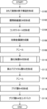
- FIG. 3 is a flowchart illustrating an example of a manufacturing process of the semiconductor device 100.
- FIG. An example of a process for forming the oxide layer 66 will be shown.
- a modification of the process of forming the oxide layer 66 will be shown.
- a modification of the process of forming the oxide layer 66 will be shown.
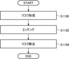
- 7 is a flowchart showing a manufacturing process of a semiconductor device according to a comparative example.
- one side in the direction parallel to the depth direction of the semiconductor substrate is referred to as "upper”, and the other side is referred to as “lower”.
- one surface is referred to as the upper surface and the other surface is referred to as the lower surface.
- the “up” and “down” directions are not limited to the gravitational direction or the direction in which the semiconductor device is mounted.
- orthogonal coordinate axes of the X-axis, Y-axis, and Z-axis only specify the relative positions of the components and do not limit specific directions.
- the Z axis does not limit the height direction relative to the ground.
- the +Z-axis direction and the -Z-axis direction are directions opposite to each other.
- the Z-axis direction is described without indicating positive or negative, it means a direction parallel to the +Z-axis and the -Z-axis.
- orthogonal axes parallel to the top and bottom surfaces of the semiconductor substrate are referred to as the X axis and the Y axis. Further, the axis perpendicular to the upper and lower surfaces of the semiconductor substrate is defined as the Z axis.
- the direction of the Z-axis may be referred to as the depth direction.
- a direction parallel to the top and bottom surfaces of the semiconductor substrate, including the X-axis and Y-axis may be referred to as a horizontal direction.
- FIG. 1A shows an example of a top view of the semiconductor device 100.
- the semiconductor device 100 of this example is a semiconductor chip including a transistor section 70.
- the semiconductor device 100 is not limited to a transistor as long as it is a semiconductor element having a MOS gate structure on the semiconductor substrate 10.
- the transistor section 70 is a region obtained by projecting the collector region 22 provided on the back side of the semiconductor substrate 10 onto the top surface of the semiconductor substrate 10.
- the collector area 22 will be described later.
- the transistor section 70 includes a transistor such as an IGBT.
- the transistor section 70 is an IGBT.
- the transistor section 70 may be another transistor such as a MOSFET.
- an edge termination structure may be provided in the negative side region in the Y-axis direction of the semiconductor device 100 of this example.
- the edge termination structure alleviates electric field concentration on the upper surface side of the semiconductor substrate 10.
- the edge termination structure includes, for example, a guard ring, a field plate, a resurf, and a combination thereof. Note that in this example, for convenience, the negative edge in the Y-axis direction will be described, but the same applies to other edges of the semiconductor device 100.
- the semiconductor substrate 10 is a substrate made of a semiconductor material.
- the semiconductor substrate 10 may be a silicon substrate, a silicon carbide substrate, a gallium nitride substrate, a diamond substrate, or another substrate.
- the semiconductor substrate 10 of this example is a silicon substrate. Note that in this specification, when simply referred to as a top view, it means viewed from the top surface side of the semiconductor substrate 10.
- the semiconductor substrate 10 has a front surface 21 and a back surface 23, as described later.
- the semiconductor device 100 of this example includes, on the front surface 21 of the semiconductor substrate 10, a gate trench section 40, a dummy trench section 30, an emitter region 12, a base region 14, a contact region 15, and a well region 17. Equipped with Further, the semiconductor device 100 of this example includes an emitter electrode 52 and a gate metal layer 50 provided above the front surface 21 of the semiconductor substrate 10. The emitter electrode 52 and the gate metal layer 50 are examples of a front side metal layer 53, which will be described later.
- the gate trench portion 40 is an example of a MOS gate structure included in the semiconductor device 100. Note that although the semiconductor device 100 of this example is a transistor with a MOS gate structure, it may be a diode with a MOS gate structure.
- the emitter electrode 52 is provided above the gate trench section 40, dummy trench section 30, emitter region 12, base region 14, contact region 15, and well region 17. Further, gate metal layer 50 is provided above connection portion 25 and well region 17 .
- the emitter electrode 52 and the gate metal layer 50 are formed of a material containing metal. At least a portion of the emitter electrode 52 may be formed of a metal such as aluminum (Al) or a metal alloy such as aluminum-silicon alloy (AlSi) or aluminum-silicon-copper alloy (AlSiCu). At least a portion of the gate metal layer 50 may be formed of a metal such as aluminum (Al) or a metal alloy such as aluminum-silicon alloy (AlSi) or aluminum-silicon-copper alloy (AlSiCu). The emitter electrode 52 and the gate metal layer 50 may have a barrier metal layer made of titanium, a titanium compound, or the like below a region made of aluminum or the like. The barrier metal layer will be described later. Emitter electrode 52 and gate metal layer 50 are provided separately from each other.
- the emitter electrode 52 and the gate metal layer 50 are provided above the semiconductor substrate 10 with the interlayer insulating film 38 in between.
- the interlayer insulating film 38 is omitted in FIG. 1A.
- a contact hole 54, a contact hole 55, and a contact hole 56 are provided through the interlayer insulating film 38.
- the contact hole 55 electrically connects the gate metal layer 50 and the gate conductive part in the transistor section 70 via the connection part 25.
- a plug layer made of tungsten or the like may be formed inside the contact hole 55. The plug layer will be described later.
- the contact hole 56 connects the emitter electrode 52 and the dummy conductive part within the dummy trench part 30.
- a plug layer made of tungsten or the like may be formed inside the contact hole 56.
- the connecting portion 25 is connected to the emitter electrode 52 or the front metal layer 53 such as the gate metal layer 50.
- connection portion 25 is provided between gate metal layer 50 and gate conductive portion.
- the connecting portion 25 in this example is provided extending in the X-axis direction, and may be electrically connected to the gate conductive portion.
- the connecting portion 25 may also be provided between the emitter electrode 52 and the dummy conductive portion. In this example, the connection portion 25 is not provided between the emitter electrode 52 and the dummy conductive portion.
- the connection portion 25 is made of a conductive material such as polysilicon doped with impurities.
- the connection portion 25 in this example is polysilicon (N+) doped with N-type impurities.
- the connecting portion 25 is provided above the front surface 21 of the semiconductor substrate 10 via an insulating film such as an oxide film.
- the gate trench portion 40 is an example of a plurality of trench portions extending in a predetermined stretching direction on the front surface 21 side of the semiconductor substrate 10.
- the gate trench portions 40 are arranged at predetermined intervals along a predetermined arrangement direction (in this example, the X-axis direction).
- the gate trench portion 40 of this example includes two extending portions 41 that extend along a stretching direction (Y-axis direction in this example) that is parallel to the front surface 21 of the semiconductor substrate 10 and perpendicular to the arrangement direction. It may have a connecting portion 43 that connects the two extending portions 41.
- the connecting portion 43 is formed in a curved shape.
- the gate metal layer 50 may be electrically connected to the gate conductive portion via the connection portion 25.
- the dummy trench portion 30 is an example of a plurality of trench portions extending in a predetermined stretching direction on the front surface 21 side of the semiconductor substrate 10.
- the dummy trench section 30 is a trench section electrically connected to the emitter electrode 52.
- the dummy trench sections 30 are arranged at predetermined intervals along a predetermined arrangement direction (in this example, the X-axis direction).
- the dummy trench section 30 of this example has an I-shape on the front surface 21 of the semiconductor substrate 10, but similarly to the gate trench section 40, it has a U-shape on the front surface 21 of the semiconductor substrate 10. It's okay. That is, the dummy trench portion 30 may have two extending portions extending along the extending direction and a connecting portion connecting the two extending portions.
- the transistor section 70 of this example has a structure in which two gate trench sections 40 and two dummy trench sections 30 are repeatedly arranged. That is, the transistor section 70 of this example has the gate trench section 40 and the dummy trench section 30 at a ratio of 1:1. For example, the transistor section 70 has one dummy trench section 30 between two extended sections 41.
- the ratio of the gate trench portion 40 to the dummy trench portion 30 is not limited to this example.
- the ratio of the gate trench portion 40 may be larger than the ratio of the dummy trench portion 30, and the ratio of the dummy trench portion 30 may be larger than the ratio of the gate trench portion 40.
- the ratio of the gate trench section 40 to the dummy trench section 30 may be 2:3 or 2:4.
- the transistor section 70 may have all the trench sections as the gate trench section 40 and may not have the dummy trench section 30.
- the well region 17 is a second conductivity type region provided closer to the front surface 21 of the semiconductor substrate 10 than a drift region 18 described later.
- the well region 17 is an example of a well region provided on the peripheral side of the active section 120.
- the active section 120 will be described later.
- the well region 17 is of P+ type, for example.
- the well region 17 is formed in a predetermined range from the end of the active region on the side where the gate metal layer 50 is provided.
- the diffusion depth of the well region 17 may be deeper than the depths of the gate trench section 40 and the dummy trench section 30.
- Some regions of the gate trench portion 40 and the dummy trench portion 30 on the gate metal layer 50 side are formed in the well region 17 .
- the bottoms of the ends of the gate trench portion 40 and the dummy trench portion 30 in the extending direction may be covered with the well region 17 .
- the contact hole 54 is formed above each of the emitter region 12 and the contact region 15 in the transistor section 70. Contact hole 54 is not provided above well region 17 provided at both ends in the Y-axis direction. In this way, one or more contact holes 54 are formed in the interlayer insulating film. One or more contact holes 54 may be provided extending in the stretching direction.
- the mesa portion 71 is a mesa portion provided adjacent to the trench portion in a plane parallel to the front surface 21 of the semiconductor substrate 10.
- the mesa portion is a portion of the semiconductor substrate 10 sandwiched between two adjacent trench portions, and is a portion from the front surface 21 of the semiconductor substrate 10 to the depth of the deepest bottom of each trench portion. good.
- the extending portion of each trench portion may be one trench portion. That is, the area sandwiched between the two extended parts may be used as the mesa part.
- the mesa portion 71 is provided adjacent to at least one of the dummy trench portion 30 or the gate trench portion 40 in the transistor portion 70 .
- Mesa portion 71 includes well region 17 , emitter region 12 , base region 14 , and contact region 15 on front surface 21 of semiconductor substrate 10 .
- emitter regions 12 and contact regions 15 are provided alternately in the extending direction.
- the base region 14 is a second conductivity type region provided on the front surface 21 side of the semiconductor substrate 10.
- the base region 14 is, for example, P-type.
- the base region 14 may be provided at both ends of the mesa portion 71 in the Y-axis direction on the front surface 21 of the semiconductor substrate 10 . Note that FIG. 1A shows only one end of the base region 14 in the Y-axis direction.
- the emitter region 12 is a region of the first conductivity type that has a higher doping concentration than the drift region 18.
- the emitter region 12 in this example is of N+ type, for example.
- An example of a dopant in emitter region 12 is arsenic (As).
- Emitter region 12 is provided on front surface 21 of mesa portion 71 in contact with gate trench portion 40 .
- the emitter region 12 may be provided extending in the X-axis direction from one of the two trench portions sandwiching the mesa portion 71 to the other. Emitter region 12 is also provided below contact hole 54 .
- the emitter region 12 may or may not be in contact with the dummy trench portion 30.
- the emitter region 12 in this example is in contact with the dummy trench section 30.
- the contact region 15 is provided above the base region 14 and is a second conductivity type region having a higher doping concentration than the base region 14.
- the contact region 15 in this example is of P+ type, for example.
- the contact region 15 in this example is provided on the front surface 21 of the mesa portion 71.
- the contact region 15 may be provided in the X-axis direction from one of the two trench portions with the mesa portion 71 in between to the other.
- the contact region 15 may or may not be in contact with the gate trench section 40 or the dummy trench section 30.
- Contact region 15 in this example contacts dummy trench section 30 and gate trench section 40 .
- Contact region 15 is also provided below contact hole 54 .
- FIG. 1B shows an example of the aa' cross section in FIG. 1A.
- the aa' cross section is an XZ plane passing through the emitter region 12 in the transistor section 70.
- the semiconductor device 100 of this example includes a semiconductor substrate 10, an interlayer insulating film 38, an emitter electrode 52, and a collector electrode 24 in the aa' cross section.
- the collector electrode 24 is an example of a backside metal layer provided in contact with the backside 23 of the semiconductor substrate 10 .
- Emitter electrode 52 is formed above semiconductor substrate 10 and interlayer insulating film 38 .
- the drift region 18 is a first conductivity type region provided in the semiconductor substrate 10.
- the drift region 18 in this example is of N- type, for example.
- Drift region 18 may be a region in semiconductor substrate 10 that remains without other doped regions being formed. That is, the doping concentration of the drift region 18 may be the doping concentration of the semiconductor substrate 10.
- the buffer region 20 is a first conductivity type region provided closer to the back surface 23 of the semiconductor substrate 10 than the drift region 18 is.
- the buffer region 20 in this example is of N type, for example.
- the doping concentration of buffer region 20 is higher than the doping concentration of drift region 18 .
- the buffer region 20 may function as a field stop layer that prevents a depletion layer spreading from the lower surface side of the base region 14 from reaching the collector region 22 of the second conductivity type. Note that the buffer area 20 may be omitted.
- the collector region 22 is provided below the buffer region 20 in the transistor section 70.
- Collector region 22 has a second conductivity type.
- the collector region 22 in this example is of P+ type, for example.
- the collector electrode 24 is formed on the back surface 23 of the semiconductor substrate 10.
- Collector electrode 24 is formed of a conductive material such as metal.
- the material of the collector electrode 24 may be the same as or different from the material of the emitter electrode 52.
- the base region 14 is a second conductivity type region provided above the drift region 18. Base region 14 is provided in contact with gate trench portion 40 . The base region 14 may be provided in contact with the dummy trench section 30.
- the emitter region 12 is provided above the base region 14. Emitter region 12 is provided between base region 14 and front surface 21 . Emitter region 12 is provided in contact with gate trench portion 40 . The emitter region 12 may or may not be in contact with the dummy trench portion 30.
- the accumulation region 16 is a first conductivity type region provided closer to the front surface 21 of the semiconductor substrate 10 than the drift region 18 is.
- the storage region 16 in this example is of N+ type, for example. However, the storage area 16 may not be provided.
- Accumulation region 16 is provided in contact with gate trench portion 40 .
- the accumulation region 16 may or may not be in contact with the dummy trench portion 30.
- the doping concentration of the accumulation region 16 is higher than the doping concentration of the drift region 18.
- the dose of ion implantation into the storage region 16 may be 1.0E+12 cm -2 or more and 1.0E+13 cm -2 or less. Further, the ion implantation dose of the accumulation region 16 may be 3.0E+12 cm -2 or more and 6.0E+12 cm -2 or less.
- One or more gate trench sections 40 and one or more dummy trench sections 30 are provided on the front surface 21.
- Each trench portion is provided from the front surface 21 to the drift region 18. In a region where at least one of emitter region 12, base region 14, contact region 15, and storage region 16 is provided, each trench portion also passes through these regions and reaches drift region 18.
- the trench portion penetrating the doping region is not limited to manufacturing in the order in which the doping region is formed and then the trench portion is formed.
- a structure in which a doping region is formed between the trench sections after the trench section is formed is also included in the structure in which the trench section penetrates the doping region.
- the gate trench portion 40 includes a gate trench formed on the front surface 21, a gate insulating film 42, and a gate conductive portion 44.
- the gate insulating film 42 is formed to cover the inner wall of the gate trench.
- the gate insulating film 42 may be formed by oxidizing or nitriding the semiconductor on the inner wall of the gate trench.
- the gate conductive portion 44 is formed inside the gate trench and inside the gate insulating film 42 .
- the gate insulating film 42 insulates the gate conductive portion 44 and the semiconductor substrate 10.
- Gate conductive portion 44 is formed of a conductive material such as polysilicon.
- Gate trench portion 40 is covered with interlayer insulating film 38 on front surface 21 .
- the gate conductive portion 44 includes a region facing the adjacent base region 14 on the mesa portion 71 side with the gate insulating film 42 in between in the depth direction of the semiconductor substrate 10 .
- a predetermined voltage is applied to the gate conductive portion 44, a channel is formed by an electron inversion layer in the surface layer of the interface of the base region 14 that is in contact with the gate trench.
- the dummy trench section 30 may have the same structure as the gate trench section 40.
- the dummy trench section 30 includes a dummy trench formed on the front surface 21 side, a dummy insulating film 32, and a dummy conductive section 34.
- the dummy insulating film 32 is formed to cover the inner wall of the dummy trench.
- the dummy conductive portion 34 is formed inside the dummy trench and inside the dummy insulating film 32 .
- the dummy insulating film 32 insulates the dummy conductive portion 34 and the semiconductor substrate 10.
- the dummy trench portion 30 may be covered with an interlayer insulating film 38 on the front surface 21 .
- the interlayer insulating film 38 is provided above the semiconductor substrate 10.
- the interlayer insulating film 38 of this example is provided in contact with the front surface 21.
- An emitter electrode 52 is provided above the interlayer insulating film 38.
- the interlayer insulating film 38 is provided with one or more contact holes 54 for electrically connecting the emitter electrode 52 and the semiconductor substrate 10. Similarly, the contact hole 55 and the contact hole 56 may be provided to penetrate the interlayer insulating film 38.
- the thickness of the interlayer insulating film 38 is, for example, 1.0 ⁇ m, but is not limited thereto.
- the interlayer insulating film 38 may be a silicon oxide film.
- the interlayer insulating film 38 may be a BPSG (boro-phosphosilicate glass) film, a BSG (borosilicate glass) film, or a PSG (phosphosilicate glass) film.
- the interlayer insulating film 38 may include a high temperature silicon oxide (HTO) film.
- the backside lifetime control region 151 may be provided in the transistor section 70. However, the back side lifetime control area 151 may be omitted.
- the backside lifetime control region 151 is a region in which a lifetime killer is intentionally formed by, for example, injecting impurities into the inside of the semiconductor substrate 10 .
- the backside lifetime control region 151 is formed by implanting helium into the semiconductor substrate 10.
- the backside lifetime control region 151 may be formed by injection of protons.
- Lifetime killer is the center of career recombination.
- the lifetime killer may be a lattice defect.
- the lifetime killer may be a vacancy, a double vacancy, a composite defect of these and an element constituting the semiconductor substrate 10, or a dislocation.
- the lifetime killer may be a rare gas element such as helium or neon, or a metal element such as platinum. Electron beams and protons may be used to form lattice defects.
- the lifetime killer concentration is the recombination center concentration of carriers.
- the lifetime killer concentration may be the concentration of lattice defects.
- the lifetime killer concentration may be the concentration of vacancies such as vacancies and double vacancies, the composite defect concentration of these vacancies and elements constituting the semiconductor substrate 10, or the concentration of dislocations. It's good to be there.
- the lifetime killer concentration may be a chemical concentration of a rare gas element such as helium or neon, or a chemical concentration of a metal element such as platinum.
- the backside lifetime control region 151 is provided closer to the backside 23 than the center of the semiconductor substrate 10 in the depth direction of the semiconductor substrate 10 .
- the back side lifetime control area 151 in this example is provided in the buffer area 20.
- the backside lifetime control region 151 of this example is provided on the entire surface of the semiconductor substrate 10 in the XY plane, and can be formed without using a mask.
- the backside lifetime control region 151 may be provided in a part of the semiconductor substrate 10 in the XY plane.
- the dose of impurities for forming the back side lifetime control region 151 may be 0.5E+10 cm -2 or more and 1.0E+14 cm -2 or less, or 5.0E+10 cm -2 or more and 1.0E+13 cm -2 or less. There may be.
- the backside lifetime control region 151 may be formed by injection from the backside 23 side. This makes it easier to avoid the influence on the front surface 21 side of the semiconductor device 100.
- the backside lifetime control region 151 is formed by irradiating helium or protons from the backside 23 side.
- whether the back surface side lifetime control region 151 is formed by injection from the front surface 21 side or from the back surface 23 side can be determined by the SR method or leakage current measurement. This can be determined by acquiring the state of the face 21 side.
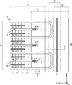
- FIG. 2A shows a top view of a modification of the semiconductor device 100. In this example, only some members of the semiconductor device 100 are shown, and some members are omitted.
- the semiconductor substrate 10 has an edge 102 when viewed from above.
- the semiconductor substrate 10 of this example has two sets of end sides 102 facing each other in a top view.
- the X-axis and Y-axis are parallel to either edge 102.
- An active part 120 is provided on the semiconductor substrate 10.
- the active region 120 is a region where a main current flows in the depth direction between the front surface 21 and the back surface 23 of the semiconductor substrate 10 when the semiconductor device 100 operates.
- An emitter electrode 52 is provided above the active region 120, but is omitted in this figure.
- the active part 120 is provided with at least one of a transistor part 70 including a transistor element such as an IGBT, and a diode part 80 including a diode element such as a free-wheeling diode (FWD).
- a transistor part 70 including a transistor element such as an IGBT and a diode part 80 including a diode element such as a free-wheeling diode (FWD).
- the transistor portions 70 and the diode portions 80 are alternately arranged along a predetermined arrangement direction (X-axis direction in this example) on the front surface 21 of the semiconductor substrate 10.
- only one of the transistor section 70 and the diode section 80 may be provided in the active section 120.
- the symbol “I” is attached to the region where the transistor section 70 is arranged
- the symbol “F” is attached to the region where the diode section 80 is arranged.
- the transistor section 70 and the diode section 80 may each have a length in the extending direction. In other words, the length of the transistor section 70 in the Y-axis direction is greater than the width in the X-axis direction. Similarly, the length of the diode section 80 in the Y-axis direction is greater than the width in the X-axis direction.
- the extending direction of the transistor section 70 and the diode section 80 may be the same as the longitudinal direction of each trench section, which will be described later.
- the diode section 80 is a region obtained by projecting the cathode region 82 provided on the back surface 23 side of the semiconductor substrate 10 onto the upper surface of the semiconductor substrate 10.
- the cathode region 82 will be described later.
- a P+ type collector region 22 may be provided on the back surface 23 of the semiconductor substrate 10.
- the diode section 80 may also include an extension region 85 in which the diode section 80 is extended in the Y-axis direction to a gate wiring to be described later.
- the collector region 22 may be provided on the back surface 23 of the extension region 85 .
- the semiconductor device 100 may have one or more pads above the semiconductor substrate 10.
- the semiconductor device 100 of this example has a gate pad 112.
- the semiconductor device 100 may have pads such as an anode pad and a cathode pad. Each pad is arranged near the edge 102.
- the vicinity of the edge 102 refers to the area between the edge 102 and the emitter electrode 52 in a top view.
- each pad may be connected to an external circuit via wiring such as a wire.
- a gate potential is applied to the gate pad 112.
- Gate pad 112 is electrically connected to gate conductive portion 44 of gate trench portion 40 of active portion 120 .
- the semiconductor device 100 includes a gate wiring that connects the gate pad 112 and the gate trench portion 40 . In FIG. 2A, the gate wiring is hatched.
- the gate wiring in this example includes an outer gate wiring 130 and an inter-active part gate wiring 131.
- the gate wiring may be composed of either the gate metal layer 50 or the connecting portion 25, or a combination of both as appropriate.
- the outer gate wiring 130 and the inter-active-part gate wiring 131 may have the same configuration or may have different configurations.
- the outer gate wiring 130 is arranged between the active part 120 and the edge 102 of the semiconductor substrate 10 when viewed from above.
- the outer gate wiring 130 of this example surrounds the active region 120 in a top view.
- the active portion 120 may be a region surrounded by the outer gate wiring 130 when viewed from above.
- the outer peripheral gate wiring 130 is connected to the gate pad 112.
- the outer gate wiring 130 is arranged above the semiconductor substrate 10.
- the outer gate wiring 130 may be configured by the gate metal layer 50 and the connection portion 25.
- the inter-active part gate wiring 131 is provided between the plurality of active parts 120.
- two active parts 120 are arranged side by side in the Y-axis direction.
- the inter-active part gate wiring 131 is connected to the gate trench part of the active part 120.
- the inter-active-part gate wiring 131 is arranged above the semiconductor substrate 10 .
- the inter-active-part gate wiring 131 of this example is composed of the gate metal layer 50 and the connection part 25.
- the gate metal layer 50 may be a metal layer containing aluminum or the like.
- the inter-active part gate wiring 131 may be connected to the outer peripheral gate wiring 130.
- the inter-active part gate wiring 131 of this example is provided extending in the X-axis direction from one outer peripheral gate wiring 130 to the other outer peripheral gate wiring 130 at approximately the center in the Y-axis direction so as to cross the active part 120. ing.
- the transistor parts 70 and the diode parts 80 may be arranged alternately in the X-axis direction in each divided region.
- the edge termination structure 140 is provided on the front surface 21 of the semiconductor substrate 10.
- the edge termination structure section 140 is provided between the active section 120 and the end side 102 in a top view.
- the edge termination structure section 140 of this example is arranged between the outer peripheral gate wiring 130 and the end side 102.
- the edge termination structure 140 alleviates electric field concentration on the front surface 21 side of the semiconductor substrate 10.
- the edge termination structure 140 may include at least one of a guard ring, a field plate, and a resurf provided in an annular shape surrounding the active part 120.
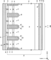
- FIG. 2B shows a top view of a modification of the semiconductor device 100.
- the semiconductor device 100 of this example includes a transistor section 70 and a diode section 80. This figure is an enlarged view of the top surface of area A in FIG. 2A.
- the semiconductor device 100 of this example includes a gate trench portion 40, a dummy trench portion 30, an emitter region 12, a base region 14, a contact region 15, and a well region 17 provided inside the front surface 21 side of the semiconductor substrate 10. Be prepared.
- Each of the gate trench section 40 and the dummy trench section 30 is an example of a trench section.
- the dummy trench section 30 of this example may have a U-shape on the front surface 21 of the semiconductor substrate 10, similarly to the gate trench section 40. That is, the dummy trench portion 30 may have two extending portions 31 extending along the extending direction and a connecting portion 33 connecting the two extending portions 31.
- the semiconductor device 100 of this example includes an emitter electrode 52 and a gate metal layer 50 provided above the front surface 21 of the semiconductor substrate 10. Emitter electrode 52 and gate metal layer 50 are provided separately from each other.
- the transistor section 70 of this example includes a boundary section 90 located at the boundary between the transistor section 70 and the diode section 80. However, the semiconductor device 100 does not need to include the boundary portion 90.
- the boundary portion 90 is a region provided in the transistor portion 70 and adjacent to the diode portion 80. Boundary portion 90 has contact region 15 on front surface 21 of semiconductor substrate 10 .
- the boundary portion 90 in this example does not have the emitter region 12.
- the trench portion of the boundary portion 90 is the dummy trench portion 30.
- the boundary portion 90 in this example is arranged such that both ends thereof in the X-axis direction serve as the dummy trench portions 30 .
- the contact hole 54 is provided above the base region 14 in the diode section 80. Contact hole 54 is provided above contact region 15 at boundary portion 90 . None of the contact holes 54 are provided above the well regions 17 provided at both ends in the Y-axis direction.
- the mesa portion 91 is provided at the boundary portion 90.
- Mesa portion 91 has contact region 15 on front surface 21 of semiconductor substrate 10 .
- the mesa portion 91 of this example has a base region 14 and a well region 17 on the negative side in the Y-axis direction.
- the mesa portion 81 is provided in a region sandwiched between adjacent dummy trench portions 30 in the diode portion 80 .
- Mesa portion 81 has base region 14 on front surface 21 of semiconductor substrate 10 .
- the mesa portion 81 of this example has the well region 17 on the negative side in the Y-axis direction.
- the emitter region 12 is provided in the mesa portion 71, it does not need to be provided in the mesa portion 81 and the mesa portion 91.
- the contact region 15 is provided in the mesa portion 71 and the mesa portion 91, it may not be provided in the mesa portion 81.
- FIG. 2C shows a bb' cross section of a modification of the semiconductor device 100.
- the semiconductor device 100 of this example includes a backside lifetime control area 151 and a front side lifetime control area 152. However, the semiconductor device 100 may not include either the back side lifetime control area 151 or the front side lifetime control area 152.
- the semiconductor device 100 of this example includes a collector region 22 and a cathode region 82 on the back surface 23 side of the buffer region 20 .
- the contact region 15 is provided above the base region 14 in the mesa portion 91. Contact region 15 is provided in mesa portion 91 in contact with dummy trench portion 30 . In other cross sections, the contact region 15 may be provided on the front surface 21 of the mesa portion 71.
- the storage region 16 is provided in the transistor section 70 and the diode section 80.
- the storage region 16 in this example is provided over the entire surface of the transistor section 70 and the diode section 80. However, the storage region 16 does not need to be provided in the diode section 80.
- the cathode region 82 is provided below the buffer region 20 in the diode section 80.
- the boundary between the collector region 22 and the cathode region 82 is the boundary between the transistor section 70 and the diode section 80. That is, the collector region 22 is provided below the boundary portion 90 in this example.
- the backside lifetime control region 151 is provided in both the transistor section 70 and the diode section 80. Thereby, the semiconductor device 100 of this example can speed up recovery in the diode section 80 and further improve switching loss.
- the back side lifetime control area 151 may be formed by the same method as the back side lifetime control area 151 of other embodiments.
- the front surface side lifetime control region 152 is provided closer to the front surface 21 than the center of the semiconductor substrate 10 in the depth direction of the semiconductor substrate 10.
- the front surface side lifetime control region 152 in this example is provided in the drift region 18 .
- the front side lifetime control region 152 is provided in both the transistor section 70 and the diode section 80.
- the front surface side lifetime control region 152 is provided at the diode section 80 and the boundary section 90, and may not be provided at a part of the transistor section 70.
- the front surface side lifetime control region 152 can suppress injection of holes from the diode section 80 and the transistor section 70 and reduce reverse recovery loss.
- the front side lifetime control region 152 may be formed by any method among the methods for forming the back side lifetime control region 151.
- the elements, doses, etc. for forming the back side lifetime control region 151 and the front side lifetime control region 152 may be the same or different.
- the front side lifetime control region 152 is provided extending from the diode section 80 to the transistor section 70.
- the front surface side lifetime control region 152 may be formed by irradiation from the front surface 21 of the semiconductor substrate 10 .
- the front surface side lifetime control region 152 may be formed by irradiation from the back surface 23 side of the semiconductor substrate 10.
- the front surface side lifetime control region 152 in this example is provided below the gate trench portion 40.
- the semiconductor device 100 may be a power semiconductor device for controlling power and the like.
- the semiconductor device 100 of this example may have a vertical semiconductor structure including a backside metal layer on the backside 23 side of the semiconductor substrate 10.
- the semiconductor device 100 may have a horizontal semiconductor structure without a metal layer on the back surface 23 side.
- an RC-IGBT with a trench gate structure is exemplified and explained as the semiconductor device 100.
- the semiconductor device 100 may be a semiconductor device with a planar gate structure, or may be another semiconductor device such as a diode.
- the semiconductor device 100 may include an N-channel MOSFET or a P-channel MOSFET.
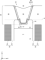
- FIG. 3A is an enlarged cross-sectional view of the semiconductor device 100.
- an enlarged view of a cross section near the contact hole 54 is shown.
- the cross section in this example is an XZ cross section passing through the emitter region 12 on the front surface 21 of the semiconductor substrate 10 .
- the emitter region 12 is an example of the first conductivity type region 161.
- the semiconductor device 100 includes a barrier metal layer 60, a first alloy layer 63, a plug layer 64, and an oxide layer 66.
- the structure near the contact hole may be explained using the contact hole 54, but the same structure may be applied to other contact holes such as the contact hole 55 and the contact hole 56.
- the barrier metal layer 60, the first alloy layer 63, the plug layer 64, and the oxide layer 66 may be provided in other contact holes such as the contact hole 55 and the contact hole 56.
- a barrier metal layer 60, a first alloy layer 63, a plug layer 64, and an oxide layer 66 may be provided for a contact hole 58, which will be described later.
- the barrier metal layer 60 is provided above the oxide layer 66 in the contact hole 54.
- Barrier metal layer 60 is provided on the bottom of contact hole 54 and on the sidewall of interlayer insulating film 38 .
- Barrier metal layer 60 may be provided in contact with the upper surface of interlayer insulating film 38 .
- Barrier metal layer 60 in this example is provided on the upper surface of oxide layer 66 and the sidewall of interlayer insulating film 38 in contact hole 54 .
- Barrier metal layer 60 includes a predetermined conductive first metal.
- the first metal is titanium (Ti), cobalt (Co), nickel (Ni), tantalum (Ta), magnesium (Mg), vanadium (V), lanthanum (La), palladium (Pd) or zirconium (Zr). There may be at least one.
- the first metal may be a metal that has a hydrogen storage effect.
- the barrier metal layer 60 of this example has a first barrier metal part 61 and a second barrier metal part 62.
- the first barrier metal portion 61 is provided on the side wall of the interlayer insulating film 38 in the contact hole 54 .
- the first barrier metal portion 61 includes a predetermined conductive first metal.
- the first barrier metal portion 61 is made of TiN.
- the first barrier metal portion 61 may be a hydrogen storage alloy.
- the first barrier metal portion 61 is formed by annealing an initial metal film containing a first metal.
- the first barrier metal portion 61 of this example is TiN, which is formed by annealing Ti deposited on the sidewall of the interlayer insulating film 38 as an initial metal film in a nitrogen atmosphere.
- the second barrier metal part 62 is stacked on the first barrier metal part 61 in the contact hole 54.
- the second barrier metal portion 62 includes a conductive material.
- the second barrier metal portion 62 is made of TiN.
- the second barrier metal portion 62 is provided in a stacked manner with the first alloy layer 63 provided on the upper surface of the semiconductor substrate 10 .
- the second barrier metal portion 62 may be formed by sputtering a conductive material.
- the second barrier metal portion 62 in this example is TiN formed by sputtering.
- the second barrier metal portion 62 may be provided in contact with the first barrier metal portion 61 and the oxide layer 66.
- the first alloy layer 63 is provided on the upper surface of the semiconductor substrate 10 below the contact hole 54.
- the first alloy layer 63 in this example is provided on the upper surface of the semiconductor substrate 10.
- the first alloy layer 63 is formed by annealing an initial metal film containing the first metal.
- the first alloy layer 63 may be an alloy consisting of the first metal and the constituent elements of the layer at the bottom of the contact hole 54 .
- the semiconductor substrate 10 is a silicon substrate
- the first alloy layer 63 may be a silicide layer.
- the semiconductor substrate 10 is a silicon carbide substrate, a gallium nitride substrate, a diamond substrate, or the like
- the first alloy layer 63 may be an alloy layer containing these substrate materials and a first metal.
- the first alloy layer 63 of this example is a titanium silicide layer formed by annealing a Ti film formed on the bottom surface of the contact hole 54 as an initial metal film.
- the N-type regions including the first conductivity type region 161 may be formed so that the N-type impurity concentration is high at the portion in contact with the first alloy layer 63, thereby reducing contact resistance.
- the first barrier metal part 61 and the first alloy layer 63 may be formed by the same annealing process.
- a first barrier metal portion 61 of TiN is formed on the sidewall of the interlayer insulating film 38, and a first alloy layer 63 of titanium silicide is formed on the upper surface of the semiconductor substrate 10.
- all of the formed initial metal film is used for forming the first barrier metal portion 61 or the first alloy layer 63, and no initial metal film may remain.
- An initial metal film may remain on the first alloy layer 63 and a metal film 67 to be described later may be formed, and the first barrier metal part 61 may be formed on the first alloy layer 63 or the metal film 67. Good too.
- the plug layer 64 is provided above the barrier metal layer 60 in the contact hole 54.
- the plug layer 64 may be provided in contact with the second barrier metal portion 62 in the contact hole 54 .
- Plug layer 64 is a conductive material filled inside contact hole 54 .
- the plug layer 64 may be made of a different material from the front metal layer 53.
- the material of the plug layer 64 is tungsten.
- the plug layer 64 may be provided above the interlayer insulating film 38 and in contact with the second barrier metal portion 62 even outside the contact hole 54 .
- the plug layer 64 may be omitted and the contact hole 54 may be filled with the front metal layer 53.
- the plug layer 64 may penetrate into the second barrier metal portion 62 as described later.
- the oxide layer 66 is provided on the upper surface of the first alloy layer 63 in the contact hole 54.
- the oxide layer 66 may be in contact with the upper surface of the first alloy layer 63 or the lower surface of the barrier metal layer 60.
- the oxide layer 66 may be provided in contact with the first alloy layer 63 and the barrier metal layer 60. That is, the oxide layer 66 may be provided in a laminated manner between the first alloy layer 63 and the barrier metal layer 60.
- the oxide layer 66 may be formed on the first barrier metal portion 61 or the metal film 67. good.
- the oxide layer 66 may be formed in the contact hole 54 on the sidewall of the interlayer insulating film 38 and under the second barrier metal portion 62.
- the oxide layer 66 may contain an element constituting the first alloy layer 63, the first barrier metal portion 61, or the metal film 67.
- the oxide layer 66 may include an oxide of an element constituting the semiconductor substrate 10 or silicon.
- oxide layer 66 is a silicon oxide film.
- the composition of the oxide layer 66 may be at least one of SiO, SiO2, or Si2O3 .
- Oxide layer 66 may include a predetermined conductive first metal.
- oxide layer 66 may include titanium and may include a titanium oxide film.
- the composition of the oxide layer 66 may be at least one of TiO, TiO2, or Ti2O3 .
- Oxide layer 66 may be a dense film that functions as a metal diffusion prevention layer.
- the oxide layer 66 can prevent diffusion of the plug layer 64 during formation of the plug layer 64 and protect the first alloy layer 63 from damage during formation of the plug layer 64.
- the thickness of the oxide layer 66 may be thinner than the thickness of the first alloy layer 63.
- the thickness of the oxide layer 66 may be thinner than the thickness of the second barrier metal portion 62.
- the thickness of the oxide layer 66 may be 0.5 nm or more and 4.0 nm or less.
- the thickness of the oxide layer 66 is 2.5 nm.
- the thickness of the oxide layer 66 may be the thickness at the thickest position in the contact hole 54 .
- the oxide layer 66 may be formed by chemical exposure such as etching.
- the oxide layer 66 may be formed by etching the upper surface of the first alloy layer 63, the first barrier metal portion 61, or the metal film 67.
- the upper surface of the first alloy layer 63, the first barrier metal portion 61, or the metal film 67 may be etched by wet etching or dry etching.
- the oxide layer 66 may be formed by dry etching the top surface of the first alloy layer 63.
- the oxide layer 66 may be formed by oxidizing the upper surface of the first alloy layer 63, the first barrier metal portion 61, or the metal film 67.
- the oxide layer 66 may be formed by annealing the semiconductor substrate 10 in an oxygen atmosphere.
- the oxide layer 66 may be formed by being deposited on the first alloy layer 63, the first barrier metal part 61, the metal film 67, or the interlayer insulating film 38.
- the interlayer insulating film 38 has a contact hole 54 and is provided above the semiconductor substrate 10.
- the interlayer insulating film 38 has one layer of insulating film provided above the front surface 21, but may have a plurality of laminated insulating films.
- the interlayer insulating film 38 may be a silicon oxide film such as BPSG.
- the first barrier metal part 61 is denser than the second barrier metal part 62.
- the first barrier metal portion 61 and the second barrier metal portion 62 may be formed using different film forming methods.
- the first barrier metal portion 61 may be a TiN film formed by annealing Ti deposited on the sidewall of the interlayer insulating film 38 .
- the second barrier metal portion 62 may be a TiN film formed by sputtering TiN. Thereby, the first barrier metal part 61 may become a TiN film denser than the second barrier metal part 62.
- the first barrier metal portion 61 and the second barrier metal portion 62 may include the same material.
- the first barrier metal portion 61 By forming the first barrier metal portion 61 densely, it is possible to protect the interlayer insulating film 38 from damage during the formation of the plug layer 64.
- the second barrier metal portion 62 formed by sputtering does not require the formation of an initial metal film, it is possible to avoid the influence of the hydrogen storage effect caused by remaining Ti or the like.
- the plug layer 64 may invade the second barrier metal part 62 when the plug layer 64 is formed.
- the film thickness of the first barrier metal part 61 may be thinner than the film thickness of the second barrier metal part 62.
- the thickness of the first barrier metal portion 61 may be thinner than the thickness of the first alloy layer 63.
- the first barrier metal portion 61 may be thinned by etching after forming a dense film. Etching after a dense film is formed may be performed using a chemical solution.
- the chemical solution for etching may be, for example, hydrofluoric acid (hydrofluoric acid), ammonia peroxide, sulfuric acid, or the like.
- Ammonia peroxide is a liquid mixture of ammonia (NH 4 OH), hydrogen peroxide (H 2 O 2 ) and water (H 2 O).
- Etching after the dense film is formed may be dry etching, reverse sputtering, or the like.
- the film thickness of the first barrier metal portion 61 may be 1 nm or more and 10 nm or less.
- the thickness of the first barrier metal portion 61 may be the thickness at the thickest position in the contact hole 54 .
- the thickness of the first barrier metal portion 61 may be formed within a predetermined range over the entire sidewall of the interlayer insulating film 38 .
- the film thickness of the second barrier metal portion 62 may be 1 nm or more and 100 nm or less.
- the thickness of the first alloy layer 63 may be 1 nm or more and 200 nm or less.
- the first barrier metal portion 61 may cover the sidewall of the interlayer insulating film 38.
- the lower end of the first barrier metal portion 61 may be in contact with the oxide layer 66 . That is, the bottom surface of contact hole 54 and the sidewall of interlayer insulating film 38 may be covered with oxide layer 66 and first barrier metal portion 61, respectively. Thereby, the interlayer insulating film 38 and the first alloy layer 63 can be prevented from being eroded by the gas during the formation of the plug layer 64.
- the opening width W54 of the contact hole 54 is the width of the contact hole 54 in the trench arrangement direction on the upper surface of the interlayer insulating film 38.
- the opening width W54 of the contact hole 54 may be greater than or equal to 100 nm and less than or equal to 1000 nm.
- defects may occur near the interface between the oxide film and the semiconductor layer of the MOS gate structure. If a metal such as Ti, which has a hydrogen storage effect, exists near the MOS gate structure, it will absorb the hydrogen that diffuses into the gate, inhibiting hydrogen termination of the dangling bonds in the MOS gate structure, and lowering the threshold voltage. It may change.
- An unreacted initial metal film having a hydrogen storage effect may remain on the upper surface of the first alloy layer 63.
- the semiconductor device 100 of this example by etching and oxidizing the upper surface of the first alloy layer 63, the remaining amount of the initial metal film having a hydrogen storage effect can be reduced, and the oxide layer 66 can be formed.
- the semiconductor device 100 of this example by making the first barrier metal portion 61 thin, it is possible to reduce the remaining amount of the first metal that has a hydrogen storage effect. This makes it possible to suppress the influence of the hydrogen storage effect and promote hydrogen termination of dangling bonds in the MOS gate structure. Thereby, fluctuations in threshold voltage can be suppressed.
- the semiconductor device 100 can ensure barrier properties when forming the plug layer 64.
- the semiconductor device 100 of this example can suppress fluctuations in threshold voltage while increasing reliability on the front surface 21 side. Further, since the semiconductor device 100 can form a lifetime control region while suppressing fluctuations in threshold voltage, reverse recovery loss can be reduced.
- the electron beam and particle beam for forming the lifetime control region have a greater influence on the MOS gate structure when irradiated from the front surface 21 side of the semiconductor substrate 10; Even when irradiating from the side, the MOS gate structure may be affected. Therefore, even when the semiconductor device 100 is irradiated from the back surface 23 side, damage to the MOS gate structure can be recovered and fluctuations in the threshold voltage can be suppressed.
- the accelerating voltage increases and the device becomes larger; however, in the semiconductor device 100 of this example, the particle beam or the like is irradiated from the front surface 21. Since the influence can be suppressed, a lifetime control region can be formed with a smaller device.
- the first conductivity type region 161 is a first conductivity type region provided on the front surface 21 of the semiconductor substrate 10 and has a higher doping concentration than the drift region 18.
- the first conductivity type region 161 may be an N type region of the transistor section 70.
- the first conductivity type region 161 in this example is the emitter region 12, but is not limited thereto.
- the first conductivity type region 161 may be an N type region of a MOSFET.
- the first conductivity type region 161 may be an N type region provided outside the transistor section 70.
- the first conductivity type region 161 may be an N type region of a temperature sensing diode.
- the first conductivity type region 161 may be an N type region of a diode portion of an RC-IGBT or the like.
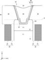
- FIG. 3B is an enlarged cross-sectional view of the semiconductor device 100.
- the cross section of this example differs from the cross section of FIG. 3A in that it passes through the contact region 15 on the front surface 21.
- Contact region 15 is an example of second conductivity type region 162. In this example, differences from FIG. 3A will be particularly explained.
- the second conductivity type region 162 is a second conductivity type region provided on the front surface 21 of the semiconductor substrate 10.
- the second conductivity type region 162 may be a P-type region of the transistor section 70.
- the second conductivity type region 162 in this example is the contact region 15, but is not limited thereto.
- the second conductivity type region 162 may be a P type region of a MOSFET.
- the second conductivity type region 162 may be a P-type region provided outside the transistor section 70.
- the second conductivity type region 162 may be a P-type region of a temperature sense diode.
- the second conductivity type region 162 may be a P type region of a diode portion of an RC-IGBT or the like.
- the structure of the contact hole 54 above the second conductivity type region 162 may be the same as or different from the structure of the contact hole 54 above the first conductivity type region 161. That is, the film thicknesses of the barrier metal layer 60, the first alloy layer 63, and the oxide layer 66 may be the same above the first conductivity type region 161 and above the second conductivity type region 162, respectively. In this example, the thickness of the oxide layer 66 provided above the second conductivity type region 162 is the same as the thickness of the oxide layer 66 provided above the first conductivity type region 161; May be different. The thickness of the oxide layer 66 may be thinner above the second conductivity type region 162 than above the first conductivity type region 161.
- the P-type regions including the second conductivity type region 162 may be formed such that the P-type impurity is concentrated at a high concentration at the portions in contact with the first alloy layer 63, thereby reducing contact resistance.
- FIG. 4A is an enlarged cross-sectional view of the semiconductor device 100.
- the cross section in this example is an XZ cross section passing through the emitter region 12 on the front surface 21 of the semiconductor substrate 10 .
- the semiconductor device 100 of this example differs from the example of FIG. 3A in that it does not include the first barrier metal part 61 and includes a metal film 67 between the second barrier metal part 62 and the interlayer insulating film 38.
- the metal film 67 may be formed by remaining the initial metal film. That is, in the step of forming the first alloy layer 63, the initial metal film may remain, and even after the etching in the step of forming the oxide layer 66, a part of the initial metal film may remain, and the metal film 67 may remain. may be formed.
- the metal film 67 may be denser than the second barrier metal portion 62.
- the metal film 67 is provided on the sidewall of the interlayer insulating film 38 in the contact hole 54 .
- the metal film 67 may be provided in contact with the upper surface of the interlayer insulating film 38.
- the second barrier metal portion 62 is provided on the bottom surface of the contact hole 54 and the sidewall of the interlayer insulating film 38 .
- the second barrier metal portion 62 may be provided above the interlayer insulating film 38, and the metal film 67 may be provided between the second barrier metal portion 62 and the interlayer insulating film 38.
- the second barrier metal portion 62 in this example is provided on the upper surface of the oxide layer 66 and the sidewall of the interlayer insulating film 38 in the contact hole 54, and the metal film 67 is provided on the sidewall of the interlayer insulating film 38 and the second barrier metal portion 62. established between.
- the first barrier metal portion 61 may not be formed or may be formed.
- the oxide layer 66 is formed after the first barrier metal portion 61 is formed on the surface of the metal film 67 by annealing in the step of forming the first alloy layer 63.
- the entire first barrier metal portion 61 may be removed by etching in the forming process.
- FIG. 4B is an enlarged cross-sectional view of the semiconductor device 100.
- the cross section in this example is an XZ plane that passes through the contact region 15 on the front surface 21 of the semiconductor substrate 10 .
- the semiconductor device 100 of this example differs from the example of FIG. 3B in that it does not include the first barrier metal part 61 and includes a metal film 67 between the second barrier metal part 62 and the interlayer insulating film 38.
- the semiconductor device 100 since the semiconductor device 100 includes the oxide layer 66, barrier properties can be ensured when the plug layer 64 is formed. Further, since the metal film 67 is thinned by etching in the step of forming the oxide layer 66, the influence of the hydrogen storage effect can be suppressed and hydrogen termination of the dangling bonds in the MOS gate structure can be promoted. Thereby, fluctuations in threshold voltage can be suppressed.
- FIG. 5A is an enlarged cross-sectional view of the semiconductor device 100.
- the cross section in this example is an XZ cross section passing through the emitter region 12 on the front surface 21 of the semiconductor substrate 10 .
- the semiconductor device 100 of this example differs from the embodiments of FIGS. 3A and 4A in that a metal film 67 is provided between the first barrier metal part 61 and the interlayer insulating film 38.
- the metal film 67 may be formed by remaining the initial metal film.
- the first barrier metal portion 61 is formed by the annealing process in the step of forming the first alloy layer 63, and the metal film 67 remains. A portion of the first barrier metal portion 61 may remain even after etching in the step of forming the oxide layer 66.
- the metal film 67 is provided on the sidewall of the interlayer insulating film 38 in the contact hole 54 .
- the metal film 67 may be provided in contact with the upper surface of the interlayer insulating film 38.
- Barrier metal layer 60 is provided on the bottom of contact hole 54 and on the sidewall of interlayer insulating film 38 .
- the barrier metal layer 60 may be provided above the interlayer insulating film 38, or the metal film 67 may be provided between the interlayer insulating film 38 and the barrier metal layer 60.
- the barrier metal layer 60 of this example is provided on the upper surface of the oxide layer 66 and the sidewall of the interlayer insulating film 38 in the contact hole 54, and the metal film 67 is provided between the sidewall of the interlayer insulating film 38 and the barrier metal layer 60. provided.
- FIG. 5B is an enlarged cross-sectional view of the semiconductor device 100.
- the cross section in this example is an XZ plane that passes through the contact region 15 on the front surface 21 of the semiconductor substrate 10 .
- the semiconductor device 100 of this example differs from the embodiments of FIGS. 3B and 4B in that a metal film 67 is provided between the first barrier metal part 61 and the interlayer insulating film 38.
- the semiconductor device 100 since the semiconductor device 100 includes the oxide layer 66, barrier properties can be ensured during the formation of the plug layer 64. Furthermore, since the first barrier metal portion 61 is thinned by etching in the process of forming the oxide layer 66, it is possible to suppress the influence of the hydrogen storage effect and promote hydrogen termination of the dangling bonds in the MOS gate structure. can. Thereby, fluctuations in threshold voltage can be suppressed.
- FIG. 6A is an enlarged cross-sectional view of the semiconductor device 100.
- an enlarged view of a cross section near the contact hole 54 is shown.
- the cross section in this example is an XZ cross section passing through the emitter region 12 on the front surface 21 of the semiconductor substrate 10 .
- the semiconductor device 100 of this example differs from the example of FIG. 3A in that it does not include the first barrier metal part 61.
- the barrier metal layer 60 has a second barrier metal part 62.
- the barrier metal layer 60 does not need to have the first barrier metal part 61.
- the first barrier metal portion 61 formed when forming the first alloy layer 63 and/or the initial metal film remaining after the first barrier metal portion 61 is not formed may be removed by etching.
- the second barrier metal portion 62 in this example may be provided in contact with the sidewall of the interlayer insulating film 38. Note that the second barrier metal portion 62 may be provided above the interlayer insulating film 38.
- the film thickness D66a is the thickness of the oxide layer 66 in the depth direction of the semiconductor substrate 10.
- the film thickness D66a may be the thickness of the oxide layer 66 above the first conductivity type region 161 in the depth direction of the semiconductor substrate 10.
- the film thickness D66a may be the film thickness at the thickest position of the oxide layer 66.
- the film thickness D66a may be thinner than the film thickness of the first alloy layer 63.
- FIG. 6B is an enlarged cross-sectional view of the semiconductor device 100.
- the cross section of this example differs from the cross section of FIG. 6A in that it passes through the contact region 15 on the front surface 21. In this example, differences from FIG. 6A will be particularly explained.
- the film thickness D66b is the thickness of the oxide layer 66 in the depth direction of the semiconductor substrate 10.
- the film thickness D66b is the thickness of the oxide layer 66 above the second conductivity type region 162 in the depth direction of the semiconductor substrate 10.
- the film thickness D66b may be thinner than the film thickness of the first alloy layer 63.
- the film thickness D66b of the oxide layer 66 above the second conductivity type region 162 in this example is thinner than the film thickness D66a of the oxide layer 66 above the first conductivity type region 161.
- the oxide layer 66 may be selectively etched above the second conductivity type region 162.
- the oxide layer 66 may be formed separately above the first conductivity type region 161 and above the second conductivity type region 162 to provide the oxide layer 66 with different thicknesses.
- the thickness of the oxide layer 66 above the second conductivity type region 162 is thinner than the thickness of the oxide layer 66 above the first conductivity type region 161;
- the thickness of the oxide layer 66 above the second conductivity type region 162 may be thin.
- the oxide layer 66 is formed above the first conductivity type region 161 and above the second conductivity type region 162. may have different thicknesses.
- FIG. 7A is an enlarged cross-sectional view of the semiconductor device 100.
- the cross section in this example is an XZ cross section passing through the emitter region 12 on the front surface 21 of the semiconductor substrate 10 .
- the semiconductor device 100 of this example differs from the example of FIG. 3A in that a barrier metal layer 60 and a plug layer 64 are provided outside the contact hole 54 and above the interlayer insulating film 38.
- the barrier metal layer 60 may be provided in contact with the upper surface of the interlayer insulating film 38 outside the contact hole 54.
- the plug layer 64 may be provided above the interlayer insulating film 38 and in contact with the second barrier metal portion 62 outside the contact hole 54 .
- only the barrier metal layer 60 may be provided outside the contact hole 54 and the plug layer 64 may be formed only inside the contact hole 54.
- the barrier metal layer 60 and the plug layer 64 may not have the first barrier metal portion 61 formed both outside and inside the contact hole 54, and the metal film 67 may be formed between the barrier metal layer 60 and the interlayer insulating film 38. .
- the barrier metal layer 60 may be provided without the first barrier metal portion 61 and only the second barrier metal portion 62 may be provided inside and outside the contact hole 54 , and the plug layer 64 may be provided with the first barrier metal portion 61 inside and outside the contact hole 54 . It may be provided only on the inside.
- FIG. 7B is an enlarged cross-sectional view of the semiconductor device 100.
- the cross section in this example is an XZ plane that passes through the contact region 15 on the front surface 21 of the semiconductor substrate 10 .
- the semiconductor device 100 of this example differs from the example of FIG. 3B in that the barrier metal layer 60 and the plug layer 64 are provided outside the contact hole 54 and above the interlayer insulating film 38.
- the semiconductor device 100 since the semiconductor device 100 includes the oxide layer 66, barrier properties can be ensured when the plug layer 64 is formed.
- the first barrier metal portion 61 and/or the metal film 67 are removed or thinned by etching in the step of forming the oxide layer 66, thereby suppressing the influence of the hydrogen absorption effect and forming the MOS gate. Hydrogen termination of dangling bonds in the structure can be promoted. Thereby, fluctuations in threshold voltage can be suppressed.
- FIG. 8A is an enlarged cross-sectional view of the semiconductor device 100.
- an enlarged view of a cross section near the contact hole 54 is shown.
- the cross section in this example is an XZ cross section passing through the emitter region 12 on the front surface 21 of the semiconductor substrate 10 .
- the semiconductor device 100 of this example differs from the example of FIG. 3A in that it includes a trench contact portion 65.
- the trench contact portion 65 has a contact hole 54 and is provided extending from the front surface 21 of the semiconductor substrate 10 in the depth direction of the semiconductor substrate 10 .
- the lower end of trench contact portion 65 in this example is shallower than the lower end of emitter region 12 .
- the lower end of trench contact portion 65 may be deeper than the lower end of emitter region 12 .
- the lower end of trench contact portion 65 in this example is shallower than the upper end of gate conductive portion 44 .
- the lower end of trench contact portion 65 may be deeper than the upper end of gate conductive portion 44 .
- the barrier metal layer 60 may have a first barrier metal part 61 and a second barrier metal part 62 in the trench contact part 65. However, the first barrier metal part 61 may be removed and only the second barrier metal part 62 may be provided.
- the first barrier metal portion 61 is provided in contact with the sidewall of the interlayer insulating film 38 . The first barrier metal portion 61 does not need to be provided below the front surface 21.
- the first alloy layer 63 is provided in contact with the side wall of the semiconductor substrate 10 and the top surface of the semiconductor substrate 10 at the trench contact portion 65 .
- the oxide layer 66 is in contact with the first alloy layer 63.
- the oxide layer 66 is provided in a stacked manner with the first alloy layer 63.
- the oxide layer 66 is provided on the top and side surfaces of the first alloy layer 63 in the trench contact portion 65 .
- the oxide layer 66 may be provided on the entire exposed surface of the first alloy layer 63 when the oxide layer 66 is formed.
- the barrier metal layer 60 is provided in contact with the oxide layer 66 provided on the sidewall of the semiconductor substrate 10.
- the second barrier metal portion 62 in this example is provided in contact with the first barrier metal portion 61 and the oxide layer 66.
- the second barrier metal portion 62 is provided in a stacked manner with the first barrier metal portion 61 provided on the side wall of the interlayer insulating film 38 .
- the plug layer 64 is provided inside the second barrier metal portion 62 in the contact hole 54 .
- the interlayer insulating film 38 in this example has one layer of insulating film, it may have a laminated structure in which a plurality of insulating films are laminated.
- the semiconductor device 100 of this example can increase the contact area with the semiconductor substrate 10 and reduce contact resistance.
- the trench contact portion 65 in the transistor portion 70 holes can be easily extracted and latch-up can be suppressed.
- FIG. 8B is an enlarged cross-sectional view of the semiconductor device 100.
- the cross section of this example differs from the cross section of FIG. 8A in that it passes through the contact region 15 on the front surface 21. In this example, differences from FIG. 8A will be particularly explained.
- the oxide layer 66 is provided above the first conductivity type region 161 and is not provided above the second conductivity type region 162. That is, oxide layer 66 does not need to be provided above contact region 15 . After the oxide layer 66 is formed above the first conductivity type region 161 and the second conductivity type region 162, it may be selectively removed above the second conductivity type region 162. By using a mask, the oxide layer 66 is formed only above the first conductivity type region 161 and does not need to be formed above the second conductivity type region 162.
- the semiconductor device 100 of this example by removing the oxide layer 66 above the contact region 15, hole extraction can be improved and latch-up can be easily suppressed.
- the semiconductor device 100 by providing the oxide layer 66 above the emitter region 12, damage during formation of the plug layer 64 can be reduced.
- the oxide layer 66 is omitted above the second conductivity type region 162 in the semiconductor device 100 including the trench contact portion 65, but the oxide layer 66 is similarly omitted in the semiconductor device 100 not including the trench contact portion 65.
- Layer 66 may be omitted. That is, the oxide layer 66 may be omitted in any of the embodiments of FIGS. 3A, 3B, 4A, 4B, 5A, 5B, 6A, 6B, 7A, and 7B.
- the oxide layer 66 above the second conductivity type region 162 is omitted, but the oxide layer 66 above the first conductivity type region 161 may be omitted.
- the thickness of the oxide layer 66 above the first conductivity type region 161 and above the second conductivity type region 162 may be the same or different.
- FIG. 9A shows an example of the cc' cross section in FIG. 1A or FIG. 2B.
- the cc' cross section is a YZ plane passing through the inter-active part gate wiring 131.
- the inter-active-part gate wiring 131 of this example includes a gate metal layer 50 and a connection part 25.
- the gate metal layer 50 is an example of the front side metal layer 53.
- Connection portion 25 is an example of polycrystalline layer 165.
- the polycrystalline layer 165 is a polycrystalline layer provided above or inside the semiconductor substrate 10, and may be a semiconductor or a metal. Polycrystalline layer 165 in this example is a polysilicon layer.
- polycrystalline layer 165 when semiconductor substrate 10 is a silicon carbide substrate, polycrystalline layer 165 may be a polycrystalline layer containing silicon carbide, and when semiconductor substrate 10 is a gallium nitride substrate, polycrystalline layer 165 may be a polycrystalline layer containing silicon carbide.
- the polycrystalline layer 165 may be a polycrystalline layer containing gallium, and when the semiconductor substrate 10 is a diamond substrate, the polycrystalline layer 165 may be a polycrystalline layer containing diamond.
- a covering layer 68 made of polyimide or the like may be provided above the inter-active part gate wiring 131.
- the polycrystalline layer 165 may be provided above the semiconductor substrate 10 with the insulating film 26 interposed therebetween. Polycrystalline layer 165 is electrically connected to gate conductive portion 44 . Note that the polycrystalline layer 165 may be omitted and only the front side metal layer 53 may function as the inter-active-part gate wiring 131. Alternatively, the front surface side metal layer 53 above the polycrystalline layer 165 may be omitted, and only the polycrystalline layer 165 may function as the inter-active-part gate wiring 131. In this example, the cross section of the inter-active-part gate wiring 131 has been described, but the front side metal layer 53 and the polycrystalline layer 165 may be similarly provided for the outer peripheral gate wiring 130.
- the front side metal layer 53 is provided above the semiconductor substrate 10. A portion of the front metal layer 53 may be provided to overlap the polycrystalline layer 165 in the depth direction of the semiconductor substrate 10.
- the front side metal layer 53 of this example is electrically connected to the polycrystalline layer 165 via a contact hole 55 provided above the polycrystalline layer 165.
- the front side metal layer 53 may be formed of the same material as the emitter electrode 52, or may be formed of a different material from the emitter electrode 52.
- a barrier metal layer 60, a first alloy layer 63, a plug layer 64, and an oxide layer 66 may be provided in the contact hole 55.
- the contact hole 55 may be as disclosed in any of the embodiments of FIGS. 3A, 3B, 4A, 4B, 5A, 5B, 6A, 6B, 7A, 7B or 8A.
- a barrier metal layer 60, a first alloy layer 63, a plug layer 64, and an oxide layer 66 may be provided.
- the contact hole 55 may be provided with a metal film 67 as disclosed in any of the embodiments of FIGS. 4A, 4B, 5A, or 5B.
- Contact hole 55 may not be provided with oxide layer 66 as disclosed in the embodiment of FIG. 8B.
- the thickness of the oxide layer 66 may be thinner above the polycrystalline layer 165 than above the first alloy layer 63 on the semiconductor substrate 10 and mesa portions 71, 81, and 91.
- Oxide layer 66 may be omitted in contact hole 55 provided above polycrystalline layer 165.
- the film thickness of the oxide layer 66 may be thicker above the polycrystalline layer 165 than above the first alloy layer 63 on the semiconductor substrate 10 and the mesa portions 71, 81, and 91.
- the oxide layer 66 is provided in the contact hole 55 provided above the polycrystalline layer 165, and may be omitted above the first alloy layer 63 on the semiconductor substrate 10 and the mesa portions 71, 81, and 91.
- the gate resistance of the semiconductor device 100 can be adjusted. Furthermore, depending on the magnitude of the gate resistance of the semiconductor device 100, it may be adjusted whether or not the oxide layer 66 is provided above the polycrystalline layer 165. In addition to the thickness of the oxide layer 66, the size of the gate resistance of the semiconductor device 100 may be adjusted by changing the area of the contact hole 55. The magnitude of the gate resistance of the semiconductor device 100 may be adjusted by providing a resistance layer instead of the oxide layer 66.
- the contact hole 55 may be provided in the inter-active part gate wiring 131. That is, the contact hole 55 may function as a contact hole for connecting the front side metal layer 53 provided in the inter-active part gate wiring 131 and the polycrystalline layer 165. Also in the inter-active-part gate wiring 131, the gate resistance may be adjusted depending on the thickness of the oxide layer 66, the presence or absence of the oxide layer 66, the presence or absence of a resistance layer, and the area of the contact hole 55. .
- FIG. 9B shows an example of the dd' cross section in FIG. 1A or FIG. 2B.
- the dd' cross section is an XZ plane passing through the dummy trench section 30.
- the polycrystalline layer 165 may be provided within the semiconductor substrate 10.
- the dummy conductive portion 34 of this example is an example of the polycrystalline layer 165 provided in the semiconductor substrate 10.
- a contact hole 56 may be provided above the dummy conductive section 34 .
- Contact hole 56 functions as a contact hole for connecting emitter electrode 52 and polycrystalline layer 165.
- the emitter electrode 52 is an example of the front side metal layer 53.
- the presence or absence of the oxide layer 66, the thickness of the oxide layer 66, and the area of the contact hole 56 may be adjusted as appropriate.
- a barrier metal layer 60, a first alloy layer 63, a plug layer 64, and an oxide layer 66 may be provided in the contact hole 56.
- Contact hole 56 may be as disclosed in any of the embodiments of FIGS. 3A, 3B, 4A, 4B, 5A, 5B, 6A, 6B, 7A, 7B, or 8A.
- a barrier metal layer 60, a first alloy layer 63, a plug layer 64, and an oxide layer 66 may be provided.
- the contact hole 56 may be provided with a metal film 67 as disclosed in any of the embodiments of FIGS. 4A, 4B, 5A, or 5B.
- Contact hole 56 may not be provided with oxide layer 66 as disclosed in the embodiment of FIG. 8B. 1A, FIG. 2B, FIG.
- the gate conductive portion 44 and the front metal layer 53 are connected via the connecting portion 25 and the contact hole 55, and the dummy conductive portion 34 and the emitter electrode 52 are connected to each other via the connecting portion 25 and the contact hole 55. are connected via contact holes 56.
- the gate conductive part 44 and the front metal layer 53 may be connected through a contact hole 55, and the dummy conductive part 34 and the emitter electrode 52 may be connected through a connection part 25 and a contact hole 56. Good too.
- FIG. 10A shows an example of a top view of the semiconductor device 100 including the temperature sensing section 180.
- the semiconductor device 100 of this example includes a gate pad 112, a sense electrode 114, an anode pad 116, and a cathode pad 118.
- the front metal layer 53 may include a gate pad 112, a sense electrode 114, an anode pad 116, and a cathode pad 118.
- the front metal layer 53 may be electrically connected to a conductive member such as a lead frame.
- the front metal layer 53 may be electrically connected to an external electrode of the semiconductor device 100 by wire bonding or the like. Note that the number and position of the front side metal layer 53 are not limited to this example.
- the sense electrode 114 is electrically connected to a current sensing section 115 provided below the sense electrode 114.
- Sense electrode 114 detects the current flowing through current sensing section 115.
- Current sensing section 115 detects the current flowing through transistor section 70 .
- the current sensing section 115 has a structure corresponding to the transistor section 70, and simulates the operation of the transistor section 70, so that a current proportional to the current flowing through the transistor section 70 flows therethrough. By using the current sensing section 115, the current flowing through the transistor section 70 can be monitored.
- the temperature sensing section 180 is provided above or inside the semiconductor substrate 10.
- the temperature sensing section 180 of this example is provided on the well region 17 between the transistor sections 70 in the center of the semiconductor device 100.
- Temperature sensing section 180 detects the temperature of active section 120.
- the temperature sensing unit 180 may include a diode made of monocrystalline or polycrystalline silicon.
- the temperature sensing unit 180 is used to detect the temperature of the semiconductor device 100 and protect the semiconductor chip from overheating.
- Temperature sensing section 180 is connected to a constant current source. When the temperature of the semiconductor device 100 changes, the forward voltage of the current flowing through the temperature sensing section 180 changes.
- the semiconductor device 100 can detect temperature based on a change in the forward voltage of the temperature sensing section 180.
- the temperature sensing section 180 has a longitudinal direction in the Y-axis direction and a transversal direction in the X-axis direction, but is not limited thereto.
- the anode pad 116 is electrically connected to the anode region of the temperature sensing section 180.
- the anode pad 116 is electrically connected to the anode region of the temperature sensing section 180 by an anode wiring 117.
- the cathode pad 118 is electrically connected to the cathode region of the temperature sensing section 180.
- Cathode pad 118 is electrically connected to a cathode region of temperature sensing section 180 by cathode wiring 119 .
- FIG. 10B is an example of an enlarged cross-sectional view of the temperature sensing section 180.
- the temperature sensing section 180 of this example has the contact hole 58, any contact hole structure in other examples may be applied.
- the temperature sensing section 180 includes a diode provided on the semiconductor substrate 10.
- the temperature sensing unit 180 detects the temperature of the semiconductor device 100 by utilizing the fact that the current-voltage characteristics of the diode change depending on the temperature.
- the temperature sensing section 180 is arranged above the semiconductor substrate 10 with an interlayer insulating film 184 interposed therebetween.
- the interlayer insulating film 184 may be an HTO film.
- the temperature sensing section 180 may be provided above the well region 17.
- the temperature sensing section 180 of this example includes a cathode region 181, an anode region 182, an interlayer insulating film 184, a cathode electrode 186, and an anode electrode 187.
- the cathode region 181 and the anode region 182 constitute a PN diode.
- the cathode region 181 is formed of an N-type semiconductor and functions as a cathode of a PN diode.
- Anode region 182 is formed of a P-type semiconductor and functions as an anode of a PN diode.
- Cathode region 181 and anode region 182 are provided on interlayer insulating film 184.
- the material of cathode region 181 and anode region 182 may be polysilicon.
- the cathode region 181 and the anode region 182 are examples of the polycrystalline layer 165. That is, in the contact hole 58, the oxide layer 66 may or may not be provided above the cathode region 181 and the anode region 182. Oxide layer 66 may be provided only over either cathode region 181 or anode region 182. For example, the oxide layer 66 may be provided above the cathode region 181 and the oxide layer 66 may not be provided above the anode region 182. Conversely, the oxide layer 66 may be provided above the anode region 182 and not provided above the cathode region 181. Whether or not to form the oxide layer 66 may be determined in consideration of resistance so that the stability of the temperature sensing part 180 is not impaired.
- the cathode electrode 186 is electrically connected to the cathode region 181 via the contact hole 58.
- the cathode electrode 186 is an example of the front metal layer 53. That is, the cathode electrode 186 may be formed of the same material as the emitter electrode 52.
- Cathode electrode 186 is electrically connected to cathode pad 118 through cathode wiring 119 .
- the anode electrode 187 is electrically connected to the anode region 182 via the contact hole 58.
- the anode electrode 187 is an example of the front side metal layer 53. That is, the anode electrode 187 may be formed of the same material as the emitter electrode 52.
- Anode electrode 187 is electrically connected to anode pad 116 through anode wiring 117.
- the interlayer insulating film 38 is provided on the upper surface of the cathode region 181 and the anode region 182.
- a contact hole 58 may be formed in the interlayer insulating film 38 of the temperature sensing part 180.
- Element regions such as the transistor section 70 and the diode section 80 may be provided below the temperature sensing section 180.
- a collector region 22 is provided below the temperature sensing section 180 in this example. That is, the temperature sensing section 180 of this example is provided in the transistor section 70. However, the temperature sensing section 180 may be provided in the diode section 80 or may be provided in a region away from the active section 120 or near the edge termination structure section 140. Therefore, a high concentration region like the collector region 22 does not need to be formed below the temperature sensing section 180.
- FIG. 11 is a flowchart showing an example of the manufacturing process of the semiconductor device 100.
- step S100 an element structure on the front surface 21 side of the semiconductor device 100 is formed.
- Step S100 may include a step of forming a dummy trench section 30 and a gate trench section 40 as the element structure on the front surface 21 side.
- Step S100 may include a step of forming the base region 14, emitter region 12, contact region 15, etc. by ion implantation into the semiconductor substrate 10 as the element structure on the front surface 21 side.
- step S102 an interlayer insulating film 38 is formed above the semiconductor substrate 10.
- the interlayer insulating film 38 may be formed by laminating a plurality of insulating films.
- step S104 contact holes are formed by etching the interlayer insulating film 38.
- contact holes such as contact hole 54, contact hole 55, contact hole 56, and contact hole 58 may be formed in interlayer insulating film 38.
- an initial metal film for forming the first alloy layer 63 is formed.
- a predetermined initial metal film is formed on the sidewall of the interlayer insulating film 38 and the upper surface of the semiconductor substrate 10 in the contact hole 54 . That is, the initial metal film is formed so as to be in contact with the interlayer insulating film 38 and the semiconductor substrate 10.
- the initial metal film may be comprised of a first metal.
- the first alloy layer 63 may be formed by processing the initial metal film.
- the initial metal film is a Ti film formed by sputtering.
- the thickness of the initial metal film may be 1 nm or more and 100 nm or less.
- the first barrier metal portion 61 and the oxide layer 66 may be formed by processing the initial metal film.
- step S108 the semiconductor substrate 10 is annealed in a nitrogen atmosphere.
- the first alloy layer 63 is formed on the upper surface of the semiconductor substrate 10.
- the first alloy layer 63 in this example is a titanium silicide film formed by annealing a Ti film on the upper surface of the semiconductor substrate 10.
- the temperature of annealing may be 300 degrees or more and 1100 degrees or less.
- Annealing for forming the first alloy layer 63 may be performed before forming the second barrier metal portion 62.
- the first barrier metal portion 61 may be formed on the sidewall of the interlayer insulating film 38.
- the initial metal film in contact with the interlayer insulating film 38 may serve as the first barrier metal portion 61 .
- the first barrier metal portion 61 in this example is a dense TiN film formed by annealing the Ti film on the sidewall of the interlayer insulating film 38.
- a TiN film is formed as the first barrier metal part 61, but if the material of the first barrier metal part 61 is not TiN, an initial metal film of a different material may be formed. Note that there may be a metal film 67 of the first metal remaining without reacting between the interlayer insulating film 38 and the first barrier metal part 61.
- step S110 after forming the first alloy layer 63 on the upper surface of the semiconductor substrate 10, the oxide layer 66 is formed.
- the oxide layer 66 may be formed before forming the second barrier metal portion 62.
- Oxide layer 66 is formed on the top surface of first alloy layer 63 in contact hole 54 .
- the oxide layer 66 may be formed on the entire exposed surface of the first alloy layer 63 in the contact hole 54 .
- Forming oxide layer 66 may include wet etching, dry etching, annealing, and depositing. A specific method for forming the oxide layer 66 will be described later.
- the first barrier metal portion 61 and/or the metal film 67 may be etched in the step of forming the oxide layer 66. Thereby, the first barrier metal portion 61 and/or the metal film 67 may be adjusted to have a predetermined thickness.
- the first barrier metal portion 61 may be etched to a thickness of 1 nm or more and 10 nm or less.
- the first barrier metal portion 61 and/or the metal film 67 may be completely removed by etching.
- the second barrier metal portion 62 is formed.
- the second barrier metal portion 62 may be formed below the contact hole 54 by being stacked on the oxide layer 66 . If the oxide layer 66 is not formed, the second barrier metal part 62 may be formed by laminating it on the first alloy layer 63.
- the second barrier metal part 62 may be formed on the sidewall of the contact hole 54 by being stacked on the first barrier metal part 61 and/or the metal film 67.
- the second barrier metal portion 62 may be formed in contact with the interlayer insulating film 38 on the side wall of the contact hole 54 when the first barrier metal portion 61 and/or the metal film 67 are completely removed.
- the second barrier metal portion 62 in this example is a TiN film formed by sputtering.
- step S114 the semiconductor substrate 10 is annealed in a nitrogen atmosphere.
- the annealing conditions in step S114 may be the same as or different from the annealing conditions in step S108.
- the annealing in this example is performed after the second barrier metal portion 62 is formed. Annealing of the second barrier metal portion 62 may be performed before forming the plug layer 64.
- a plug layer 64 is formed.
- tungsten is formed so as to fill the inside of the contact hole 54 by a CVD (Chemical Vapor Deposition) method.
- the oxide layer 66 in this example is provided on the upper surface of the first alloy layer 63 and may function as a metal diffusion prevention layer when forming the plug layer 64.
- the oxide layer 66 when the plug layer 64 is formed by CVD, it is possible to prevent the plug layer 64 from penetrating into the first alloy layer 63.
- step S118 the plug layer 64 is etched back. As a result, unnecessary tungsten film outside the contact hole 54 may be removed.
- the etch back may be performed by dry etching or CMP (Chemical Mechanical Polishing).
- CMP Chemical Mechanical Polishing
- the metal film 67, the first barrier metal part 61, and the second barrier metal part 62 on the interlayer insulating film 38 may also be removed.
- the metal film 67, the first barrier metal part 61, and the second barrier metal part 62 on the interlayer insulating film 38 may be removed in a step different from the etch-back of the plug layer 64.
- the metal film 67, the first barrier metal part 61, and the second barrier metal part 62 on the interlayer insulating film 38 do not need to be removed. Note that step S118 may be omitted and the plug layer 64 may be left outside the contact hole 54.
- the front side metal layer 53 may be formed above the semiconductor substrate 10. Furthermore, after step S118, members on the back surface 23 side, such as the collector electrode 24, may be formed. After step S118, the back side lifetime control area 151 and the front side lifetime control area 152 may be formed.
- FIG. 12A shows an example of the process of forming the oxide layer 66.
- a method of forming the oxide layer 66 by etching will be described.
- Steps S1100 to S1104 are an example of step S110 in FIG.
- a mask is formed above the semiconductor substrate 10. For example, a mask is formed in the areas to be protected from etching. It is not necessary to form a mask on one of the first conductivity type region 161 or the second conductivity type region 162, but not on the other. A mask may be formed above the contact region 15 and no mask may be formed above the emitter region 12. If the oxide layer 66 is not formed above the polycrystalline layer 165, a mask may be formed in the contact hole 58 above the polycrystalline layer 165.
- the upper surface of the first alloy layer 63 is etched.
- the upper surface of the first alloy layer 63 is wet etched, but dry etching may also be used.
- Wet etching the top surface of the first alloy layer 63 may include wet etching using hydrogen peroxide. By wet etching, the upper surface of the first alloy layer 63 can be etched while being oxidized.
- the oxide layer 66 may be formed by oxidizing the top surface of the first alloy layer 63.
- the wet etching chemical may be hydrogen peroxide, buffered hydrofluoric acid, hydrofluoric acid or other chemical such as ammonium hydroxide.
- the first barrier metal portion 61 may be etched.
- step S1104 the mask provided above the semiconductor substrate 10 is removed. Note that step S1100 and step S1104 may be omitted. Thereafter, the process may proceed to step S112 in FIG. 11, and the second barrier metal portion 62 may be formed.
- FIG. 12B shows a modification of the process of forming the oxide layer 66.
- a method of forming the oxide layer 66 by annealing will be described.
- Steps S1110 to S1114 are an example of step S110 in FIG.
- This example differs from the example of FIG. 12A in that step S1112 is an annealing stage. In this example, differences from FIG. 12A will be particularly explained.
- step S1112 the semiconductor substrate 10 is annealed in an oxygen atmosphere. As a result, an oxide layer 66 is formed on the upper surface of the first alloy layer 63 in a region where the mask is not formed. On the other hand, on the upper surface of the first alloy layer 63, the oxide layer 66 is not formed in the region where the mask is formed. Note that even in the case where the oxide layer 66 is formed by annealing, step S1110 and step S1114 may be omitted.
- FIG. 12C shows a modification of the process of forming the oxide layer 66.
- a method of forming oxide layer 66 by deposition will be described.
- Steps S1120 to S1124 are an example of step S110 in FIG.
- This example differs from the example of FIG. 12A in that step S1122 is a deposition stage.
- differences from FIG. 12A will be particularly explained.
- the oxide layer 66 is deposited on the semiconductor substrate 10 by a CVD method, a sputtering method, or the like.
- the oxide layer 66 may be, for example, an LTO (Low Temperature Oxide) film or an HTO film.
- an oxide layer 66 is formed on the upper surface of the first alloy layer 63 in a region where the mask is not formed.
- an oxide layer 66 is formed on the upper surface of the mask in the region where the mask is formed. Note that the oxide layer 66 on the upper surface of the mask may be removed together with the mask when removing the mask in step S1124. Even when forming by deposition, step S1120 and step S1124 may be omitted.
- FIG. 13 is a flowchart showing the manufacturing process of a semiconductor device according to a comparative example. Steps S500 to S504 may be the same as steps S100 to S104 in FIG. 11, respectively.
- step S506 a Ti film and a TiN film are formed inside the contact hole.
- step S508 the semiconductor substrate 10 is annealed in a nitrogen atmosphere to form a dense TiN film from the Ti film on the sidewall of the interlayer insulating film 38.
- a titanium silicide layer is formed on the upper surface of semiconductor substrate 10.
- step S510 a plug layer 64 is formed inside the contact hole.
- step S512 the plug layer 64 is etched back.
- the Ti film and the TiN film are formed together, and the oxide layer 66 is not formed on the upper surface of the first alloy layer 63. Further, a part of the Ti film may not be nitrided and Ti, which has a hydrogen storage effect, may remain.
- the semiconductor device 100 by forming the oxide layer 66 on the upper surface of the first alloy layer 63, the first alloy layer 63 can be protected from damage during the formation of the plug layer 64. Furthermore, by removing the unreacted first metal that has a hydrogen storage effect, it is possible to terminate defects around the MOS gate structure with hydrogen, thereby suppressing fluctuations in the threshold voltage.
- SYMBOLS 10 Semiconductor substrate, 12... Emitter region, 14... Base region, 15... Contact region, 16... Accumulation region, 17... Well region, 18... Drift region, 20 ... Buffer region, 21... Front surface, 22... Collector region, 23... Back surface, 24... Collector electrode, 25... Connection portion, 26... Insulating film, 30 ... Dummy trench part, 31... Extension part, 32... Dummy insulating film, 33... Connection part, 34... Dummy conductive part, 38... Interlayer insulating film, 40... Gate Trench portion, 41... Extension portion, 42... Gate insulating film, 43... Connection portion, 44... Gate conductive portion, 50... Gate metal layer, 52... Emitter electrode, 53... ...Front side metal layer, 54...
- Cathode wiring 120... Active part, 130... Outer periphery gate wiring, 131... ⁇ Gate wiring between active parts, 140... Edge termination structure part, 151... Back side lifetime control area, 152... Front side lifetime control area, 161... First conductivity type area , 162... Second conductivity type region, 165... Polycrystalline layer, 180... Temperature sensing section, 181... Cathode region, 182... Anode region, 184... Interlayer insulating film, 186 ...Cathode electrode, 187...Anode electrode
Landscapes
- Metal-Oxide And Bipolar Metal-Oxide Semiconductor Integrated Circuits (AREA)
- Electrodes Of Semiconductors (AREA)
Priority Applications (4)
| Application Number | Priority Date | Filing Date | Title |
|---|---|---|---|
| JP2024533688A JP7694834B2 (ja) | 2022-07-11 | 2023-07-06 | 半導体装置および半導体装置の製造方法 |
| DE112023000330.0T DE112023000330T5 (de) | 2022-07-11 | 2023-07-06 | Halbleitervorrichtung und verfahren zum herstellen einer halbleitervorrichtung |
| CN202380015510.3A CN118435357A (zh) | 2022-07-11 | 2023-07-06 | 半导体装置及半导体装置的制造方法 |
| US18/749,503 US20240339517A1 (en) | 2022-07-11 | 2024-06-20 | Semiconductor device and method for manufacturing semiconductor device |
Applications Claiming Priority (2)
| Application Number | Priority Date | Filing Date | Title |
|---|---|---|---|
| JP2022-111094 | 2022-07-11 | ||
| JP2022111094 | 2022-07-11 |
Related Child Applications (1)
| Application Number | Title | Priority Date | Filing Date |
|---|---|---|---|
| US18/749,503 Continuation US20240339517A1 (en) | 2022-07-11 | 2024-06-20 | Semiconductor device and method for manufacturing semiconductor device |
Publications (1)
| Publication Number | Publication Date |
|---|---|
| WO2024014401A1 true WO2024014401A1 (ja) | 2024-01-18 |
Family
ID=89536673
Family Applications (1)
| Application Number | Title | Priority Date | Filing Date |
|---|---|---|---|
| PCT/JP2023/025207 Ceased WO2024014401A1 (ja) | 2022-07-11 | 2023-07-06 | 半導体装置および半導体装置の製造方法 |
Country Status (5)
| Country | Link |
|---|---|
| US (1) | US20240339517A1 (https=) |
| JP (1) | JP7694834B2 (https=) |
| CN (1) | CN118435357A (https=) |
| DE (1) | DE112023000330T5 (https=) |
| WO (1) | WO2024014401A1 (https=) |
Cited By (1)
| Publication number | Priority date | Publication date | Assignee | Title |
|---|---|---|---|---|
| TWI893948B (zh) * | 2024-08-20 | 2025-08-11 | 力晶積成電子製造股份有限公司 | 具有低接觸電阻的接觸件結構及其製造方法 |
Citations (4)
| Publication number | Priority date | Publication date | Assignee | Title |
|---|---|---|---|---|
| JPH0697111A (ja) * | 1992-09-11 | 1994-04-08 | Sony Corp | バリアメタルの形成方法 |
| JP2020013828A (ja) * | 2018-07-13 | 2020-01-23 | 富士電機株式会社 | 半導体装置および製造方法 |
| WO2021251011A1 (ja) * | 2020-06-09 | 2021-12-16 | 富士電機株式会社 | 半導体装置 |
| JP2022016842A (ja) * | 2020-07-13 | 2022-01-25 | 富士電機株式会社 | 半導体装置 |
Family Cites Families (6)
| Publication number | Priority date | Publication date | Assignee | Title |
|---|---|---|---|---|
| US6475893B2 (en) | 2001-03-30 | 2002-11-05 | International Business Machines Corporation | Method for improved fabrication of salicide structures |
| JP4004843B2 (ja) | 2002-04-24 | 2007-11-07 | Necエレクトロニクス株式会社 | 縦型mosfetの製造方法 |
| JP4013842B2 (ja) | 2003-06-20 | 2007-11-28 | 日産自動車株式会社 | 炭化珪素半導体装置の製造方法 |
| JP2007335554A (ja) | 2006-06-14 | 2007-12-27 | Sanyo Electric Co Ltd | 半導体装置の製造方法 |
| JP2009177102A (ja) | 2008-01-28 | 2009-08-06 | Nissan Motor Co Ltd | 半導体装置の電極の製造方法 |
| JP6822089B2 (ja) | 2016-11-16 | 2021-01-27 | 富士電機株式会社 | 炭化珪素半導体装置の製造方法、および炭化珪素半導体装置 |
-
2023
- 2023-07-06 DE DE112023000330.0T patent/DE112023000330T5/de active Pending
- 2023-07-06 CN CN202380015510.3A patent/CN118435357A/zh active Pending
- 2023-07-06 WO PCT/JP2023/025207 patent/WO2024014401A1/ja not_active Ceased
- 2023-07-06 JP JP2024533688A patent/JP7694834B2/ja active Active
-
2024
- 2024-06-20 US US18/749,503 patent/US20240339517A1/en active Pending
Patent Citations (4)
| Publication number | Priority date | Publication date | Assignee | Title |
|---|---|---|---|---|
| JPH0697111A (ja) * | 1992-09-11 | 1994-04-08 | Sony Corp | バリアメタルの形成方法 |
| JP2020013828A (ja) * | 2018-07-13 | 2020-01-23 | 富士電機株式会社 | 半導体装置および製造方法 |
| WO2021251011A1 (ja) * | 2020-06-09 | 2021-12-16 | 富士電機株式会社 | 半導体装置 |
| JP2022016842A (ja) * | 2020-07-13 | 2022-01-25 | 富士電機株式会社 | 半導体装置 |
Cited By (1)
| Publication number | Priority date | Publication date | Assignee | Title |
|---|---|---|---|---|
| TWI893948B (zh) * | 2024-08-20 | 2025-08-11 | 力晶積成電子製造股份有限公司 | 具有低接觸電阻的接觸件結構及其製造方法 |
Also Published As
| Publication number | Publication date |
|---|---|
| US20240339517A1 (en) | 2024-10-10 |
| DE112023000330T5 (de) | 2024-08-14 |
| CN118435357A (zh) | 2024-08-02 |
| JP7694834B2 (ja) | 2025-06-18 |
| JPWO2024014401A1 (https=) | 2024-01-18 |
Similar Documents
| Publication | Publication Date | Title |
|---|---|---|
| US11094810B2 (en) | Semiconductor device and manufacturing method of semiconductor device | |
| JP7803330B2 (ja) | 半導体装置および半導体装置の製造方法 | |
| CN113937159A (zh) | 半导体装置 | |
| US20240096965A1 (en) | Semiconductor device | |
| JP6984749B2 (ja) | 半導体装置の製造方法および半導体装置 | |
| JP7848526B2 (ja) | 半導体装置 | |
| WO2018052098A1 (ja) | 半導体装置およびその製造方法 | |
| WO2022004084A1 (ja) | 半導体装置 | |
| CN110546767A (zh) | 半导体装置 | |
| JP2023096841A (ja) | 半導体装置およびその製造方法 | |
| US12563813B2 (en) | Semiconductor device and method of manufacturing semiconductor device | |
| US20240072152A1 (en) | Method of manufacturing semiconductor device | |
| US20240339517A1 (en) | Semiconductor device and method for manufacturing semiconductor device | |
| US12439622B2 (en) | Semiconductor device and manufacturing method of semiconductor device | |
| JP7677444B2 (ja) | 半導体装置の製造方法および半導体装置 | |
| JP7736198B2 (ja) | 半導体装置の製造方法 | |
| US20250194207A1 (en) | Semiconductor device and manufacturing method of semiconductor device | |
| US20260082685A1 (en) | Semiconductor device and method for manufacturing semiconductor device | |
| US20260123014A1 (en) | Semiconductor device and manufacturing method thereof | |
| JP7677531B2 (ja) | 半導体装置および半導体装置の製造方法 | |
| US20250248081A1 (en) | Semiconductor device | |
| JP7364027B2 (ja) | 半導体装置およびその製造方法 | |
| WO2025009277A1 (ja) | 半導体装置 |
Legal Events
| Date | Code | Title | Description |
|---|---|---|---|
| 121 | Ep: the epo has been informed by wipo that ep was designated in this application |
Ref document number: 23839573 Country of ref document: EP Kind code of ref document: A1 |
|
| WWE | Wipo information: entry into national phase |
Ref document number: 202380015510.3 Country of ref document: CN |
|
| WWE | Wipo information: entry into national phase |
Ref document number: 112023000330 Country of ref document: DE Ref document number: 2024533688 Country of ref document: JP |
|
| 122 | Ep: pct application non-entry in european phase |
Ref document number: 23839573 Country of ref document: EP Kind code of ref document: A1 |