WO2024014358A1 - 炭化珪素基板、炭化珪素エピタキシャル基板および炭化珪素半導体装置の製造方法 - Google Patents
炭化珪素基板、炭化珪素エピタキシャル基板および炭化珪素半導体装置の製造方法 Download PDFInfo
- Publication number
- WO2024014358A1 WO2024014358A1 PCT/JP2023/024796 JP2023024796W WO2024014358A1 WO 2024014358 A1 WO2024014358 A1 WO 2024014358A1 JP 2023024796 W JP2023024796 W JP 2023024796W WO 2024014358 A1 WO2024014358 A1 WO 2024014358A1
- Authority
- WO
- WIPO (PCT)
- Prior art keywords
- silicon carbide
- main surface
- plane
- substrate
- outer peripheral
- Prior art date
- Legal status (The legal status is an assumption and is not a legal conclusion. Google has not performed a legal analysis and makes no representation as to the accuracy of the status listed.)
- Ceased
Links
Images





Classifications
-
- C—CHEMISTRY; METALLURGY
- C30—CRYSTAL GROWTH
- C30B—SINGLE-CRYSTAL GROWTH; UNIDIRECTIONAL SOLIDIFICATION OF EUTECTIC MATERIAL OR UNIDIRECTIONAL DEMIXING OF EUTECTOID MATERIAL; REFINING BY ZONE-MELTING OF MATERIAL; PRODUCTION OF A HOMOGENEOUS POLYCRYSTALLINE MATERIAL WITH DEFINED STRUCTURE; SINGLE CRYSTALS OR HOMOGENEOUS POLYCRYSTALLINE MATERIAL WITH DEFINED STRUCTURE; AFTER-TREATMENT OF SINGLE CRYSTALS OR A HOMOGENEOUS POLYCRYSTALLINE MATERIAL WITH DEFINED STRUCTURE; APPARATUS THEREFOR
- C30B23/00—Single-crystal growth by condensing evaporated or sublimed materials
- C30B23/02—Epitaxial-layer growth
- C30B23/06—Heating of the deposition chamber, the substrate or the materials to be evaporated
-
- C—CHEMISTRY; METALLURGY
- C30—CRYSTAL GROWTH
- C30B—SINGLE-CRYSTAL GROWTH; UNIDIRECTIONAL SOLIDIFICATION OF EUTECTIC MATERIAL OR UNIDIRECTIONAL DEMIXING OF EUTECTOID MATERIAL; REFINING BY ZONE-MELTING OF MATERIAL; PRODUCTION OF A HOMOGENEOUS POLYCRYSTALLINE MATERIAL WITH DEFINED STRUCTURE; SINGLE CRYSTALS OR HOMOGENEOUS POLYCRYSTALLINE MATERIAL WITH DEFINED STRUCTURE; AFTER-TREATMENT OF SINGLE CRYSTALS OR A HOMOGENEOUS POLYCRYSTALLINE MATERIAL WITH DEFINED STRUCTURE; APPARATUS THEREFOR
- C30B25/00—Single-crystal growth by chemical reaction of reactive gases, e.g. chemical vapour-deposition growth
- C30B25/02—Epitaxial-layer growth
- C30B25/18—Epitaxial-layer growth characterised by the substrate
- C30B25/20—Epitaxial-layer growth characterised by the substrate the substrate being of the same materials as the epitaxial layer
-
- C—CHEMISTRY; METALLURGY
- C30—CRYSTAL GROWTH
- C30B—SINGLE-CRYSTAL GROWTH; UNIDIRECTIONAL SOLIDIFICATION OF EUTECTIC MATERIAL OR UNIDIRECTIONAL DEMIXING OF EUTECTOID MATERIAL; REFINING BY ZONE-MELTING OF MATERIAL; PRODUCTION OF A HOMOGENEOUS POLYCRYSTALLINE MATERIAL WITH DEFINED STRUCTURE; SINGLE CRYSTALS OR HOMOGENEOUS POLYCRYSTALLINE MATERIAL WITH DEFINED STRUCTURE; AFTER-TREATMENT OF SINGLE CRYSTALS OR A HOMOGENEOUS POLYCRYSTALLINE MATERIAL WITH DEFINED STRUCTURE; APPARATUS THEREFOR
- C30B29/00—Single crystals or homogeneous polycrystalline material with defined structure characterised by the material or by their shape
- C30B29/10—Inorganic compounds or compositions
- C30B29/36—Carbides
-
- H—ELECTRICITY
- H10—SEMICONDUCTOR DEVICES; ELECTRIC SOLID-STATE DEVICES NOT OTHERWISE PROVIDED FOR
- H10D—INORGANIC ELECTRIC SEMICONDUCTOR DEVICES
- H10D30/00—Field-effect transistors [FET]
- H10D30/01—Manufacture or treatment
- H10D30/021—Manufacture or treatment of FETs having insulated gates [IGFET]
-
- H—ELECTRICITY
- H10—SEMICONDUCTOR DEVICES; ELECTRIC SOLID-STATE DEVICES NOT OTHERWISE PROVIDED FOR
- H10D—INORGANIC ELECTRIC SEMICONDUCTOR DEVICES
- H10D30/00—Field-effect transistors [FET]
- H10D30/60—Insulated-gate field-effect transistors [IGFET]
Definitions
- the present disclosure relates to a method for manufacturing a silicon carbide substrate, a silicon carbide epitaxial substrate, and a silicon carbide semiconductor device.
- This application claims priority based on Japanese Patent Application No. 2022-113414, which is a Japanese patent application filed on July 14, 2022. All contents described in the Japanese patent application are incorporated herein by reference.
- Patent Document 1 JP 2014-185055A (Patent Document 1) describes an ingot in which the difference between the maximum value and the minimum value of the lattice constant in the ⁇ 0001> direction is 0.004 nm or less.
- a silicon carbide substrate according to the present disclosure has a main surface.
- the main surface includes a central portion and an outer peripheral portion located 10 mm away from the outer peripheral edge of the main surface toward the central portion.
- the value obtained by subtracting the lattice spacing of the (11-20) plane in the central portion from the lattice spacing of the (11-20) plane in the outer peripheral portion is ⁇ 0.00081 nm or more and 0.00065 nm or less.
- the surface density of basal plane dislocations on the main surface is 700 cm -2 or more.
- FIG. 1 is a schematic plan view showing the configuration of a silicon carbide substrate according to the first embodiment.
- FIG. 2 is a schematic cross-sectional view taken along line II-II in FIG.
- FIG. 3 is a schematic cross-sectional view taken along line III-III in FIG.
- FIG. 4 is a schematic cross-sectional view taken along line IV-IV in FIG.
- FIG. 5 is a schematic partial cross-sectional view showing the configuration of the silicon carbide crystal manufacturing apparatus according to the present embodiment.
- FIG. 6 is a schematic cross-sectional view showing a silicon carbide crystal growth process.
- FIG. 7 is a schematic cross-sectional view showing a step of annealing a silicon carbide crystal.
- FIG. 1 is a schematic plan view showing the configuration of a silicon carbide substrate according to the first embodiment.
- FIG. 2 is a schematic cross-sectional view taken along line II-II in FIG.
- FIG. 3 is a schematic cross-sectional view taken along line III-III in FIG
- FIG. 8 is a flowchart schematically showing a method for manufacturing a silicon carbide semiconductor device according to this embodiment.
- FIG. 9 is a schematic cross-sectional view showing the structure of the silicon carbide epitaxial substrate according to this embodiment.
- FIG. 10 is a schematic cross-sectional view showing the process of forming the body region.
- FIG. 11 is a schematic cross-sectional view showing the process of forming a source region.
- FIG. 12 is a schematic cross-sectional view showing a step of forming a trench on the third main surface of the silicon carbide epitaxial layer.
- FIG. 13 is a schematic cross-sectional view showing the process of forming a gate insulating film.
- FIG. 14 is a schematic cross-sectional view showing the process of forming a gate electrode and an interlayer insulating film.
- FIG. 15 is a schematic cross-sectional view showing the configuration of a silicon carbide semiconductor device according to this embodiment.
- An object of the present disclosure is to provide a method for manufacturing a silicon carbide substrate, a silicon carbide epitaxial substrate, and a silicon carbide semiconductor device that can suppress the occurrence of cracks.
- Silicon carbide substrate 100 has main surface 2.
- the main surface 2 includes a central portion 30 and an outer peripheral portion 20 located 10 mm away from the outer peripheral edge 9 of the main surface 2 toward the central portion 30.
- the value obtained by subtracting the lattice spacing of the (11-20) plane in the central portion 30 from the lattice spacing of the (11-20) plane in the outer peripheral portion 20 is ⁇ 0.00081 nm or more and 0.00065 nm or less.
- the surface density of basal plane dislocations 4 on the main surface 2 is 700 cm ⁇ 2 or more.
- the basal plane dislocation 4 Since the areal density of silicon carbide substrate 100 is high, stress in silicon carbide substrate 100 can be reduced. Therefore, generation of cracks in silicon carbide substrate 100 can be suppressed.
- the areal density of basal plane dislocations 4 on main surface 2 may be 1000 cm -2 or more. Thereby, generation of cracks in silicon carbide substrate 100 can be further suppressed.
- the lattice plane of the (11-20) plane in the central part 30 The value obtained by subtracting the interval may be ⁇ 0.00054 nm or more and ⁇ 0.00017 nm or less. Thereby, generation of cracks in silicon carbide substrate 100 can be further suppressed.
- Silicon carbide substrate 100 has main surface 2.
- the main surface 2 includes a central portion 30 and an outer peripheral portion 20 located 10 mm away from the outer peripheral edge 9 of the main surface 2 toward the central portion 30.
- the value obtained by subtracting the lattice spacing of the (11-20) plane in the central portion 30 from the lattice spacing of the (11-20) plane in the outer peripheral portion 20 is ⁇ 0.00083 nm or more and ⁇ 0.00009 nm or less.
- the surface density of basal plane dislocations 4 on the main surface 2 is less than 700 cm ⁇ 2 .
- the stress in the silicon carbide substrate 100 can be reduced. can be reduced. Therefore, while suppressing the occurrence of cracks in silicon carbide substrate 100, it is possible to suppress a decrease in reliability of silicon carbide semiconductor device 400.
- the areal density of basal plane dislocations 4 on main surface 2 may be 300 cm ⁇ 2 or less. Thereby, while suppressing the occurrence of cracks in silicon carbide substrate 100, it is possible to further suppress a decrease in reliability of silicon carbide semiconductor device 400.
- the lattice plane of the (11-20) plane in the central part 30 The value obtained by subtracting the interval may be ⁇ 0.00056 nm or more and ⁇ 0.00024 nm or less.
- main surface 2 may have a diameter of 150 mm or more.
- the diameter of main surface 2 is large, it is possible to effectively suppress the occurrence of cracks in silicon carbide substrate 100.
- main surface 2 may have a diameter of 200 mm or more.
- the diameter of main surface 2 is large, it is possible to effectively suppress the occurrence of cracks in silicon carbide substrate 100.
- Silicon carbide epitaxial substrate 200 includes silicon carbide substrate 100 according to any one of (1) to (8) above, and silicon carbide epitaxial layer 60 provided on silicon carbide substrate 100. We are prepared.
- a method for manufacturing silicon carbide semiconductor device 400 according to the present disclosure includes the following steps. Silicon carbide epitaxial substrate 200 described in (9) above is prepared. Silicon carbide epitaxial substrate 200 is processed. [Details of embodiments of the present disclosure] Hereinafter, details of embodiments of the present disclosure will be described based on the drawings. In the following drawings, the same or corresponding parts are given the same reference numerals, and the description thereof will not be repeated. In the crystallographic descriptions in this specification, individual orientations are indicated by [], collective orientations are indicated by ⁇ >, individual planes are indicated by (), and collective planes are indicated by ⁇ , respectively. Regarding negative indexes, a "-" (bar) is supposed to be placed above the number in terms of crystallography, but in this specification, a negative sign is placed in front of the number.
- FIG. 1 is a schematic plan view showing the configuration of silicon carbide substrate 100 according to the first embodiment.
- silicon carbide substrate 100 has main surface 2 (second main surface 2).
- the second main surface 2 extends along each of the first direction 101 and the second direction 102.
- the first direction 101 is, for example, the ⁇ 11-20> direction, although it is not particularly limited.
- the second direction 102 is, for example, the ⁇ 1-100> direction, although it is not particularly limited.
- the off direction is, for example, the first direction 101.
- Silicon carbide substrate 100 is made of, for example, hexagonal silicon carbide.
- the polytype of hexagonal silicon carbide is, for example, 4H.
- Silicon carbide substrate 100 contains, for example, n-type impurities such as nitrogen.
- the second principal surface 2 is a ⁇ 0001 ⁇ plane or a plane inclined in the off direction with respect to the ⁇ 0001 ⁇ plane.
- the second principal surface 2 is, for example, a (0001) plane or a plane inclined in the off direction with respect to the (0001) plane.
- the first principal surface 1 (see FIG. 2) is, for example, a (000-1) plane or a plane inclined in the off direction with respect to the (000-1) plane.
- the second principal surface 2 may be, for example, a (000-1) plane or a plane inclined in the off direction with respect to the (000-1) plane.
- the first principal surface 1 (see FIG. 2) is, for example, a (0001) plane or a plane inclined in the off direction with respect to the (0001) plane.
- the outer peripheral edge 9 of the second main surface 2 has an orientation flat portion 7 and an arcuate portion 8.
- the arcuate portion 8 is continuous with the orientation flat portion 7.
- the orientation flat portion 7 extends along a first direction 101 when viewed from a direction perpendicular to the second main surface 2.
- the diameter W1 of the second main surface 2 is, for example, 150 mm.
- the diameter W1 may be 150 mm or more, or 200 mm or more.
- the upper limit of the diameter W1 is not particularly limited, but may be, for example, 300 mm or less. When viewed in a direction perpendicular to the second principal surface 2, the diameter W1 is the longest linear distance between two different points on the outer peripheral edge 9.
- the second main surface 2 has a central portion 30 and an outer peripheral portion 20.
- the central portion 30 is located at the center of the second main surface 2.
- the central portion 30 is located at the center of a circle including the arcuate portion 8.
- the outer peripheral portion 20 is located at a distance of 10 mm from the outer peripheral edge 9 of the second main surface 2 toward the central portion 30. From another point of view, the distance W2 between the outer peripheral portion 20 and the outer peripheral edge 9 in the radial direction outward from the center of the second main surface 2 is 10 mm.
- the outer circumferential portion 20 has a first outer circumferential position 21 , a second outer circumferential position 22 , a third outer circumferential position 23 , and a fourth outer circumferential position 24 .
- the first outer peripheral position 21 is located away from the central portion 30 in the first direction 101 .
- the second outer circumferential position 22 is located at a position where the first outer circumferential position 21 has rotated 90° clockwise about the center portion 30 .
- the fourth outer circumferential position 24 is located at a position where the second outer circumferential position 22 is rotated 90° clockwise about the center portion 30.
- the third outer circumferential position 23 is located at a position where the fourth outer circumferential position 24 is rotated 90° clockwise about the center portion 30.
- the fourth outer circumferential position 24, the center portion 30, and the first outer circumferential position 21 are , are located on a straight line parallel to the first direction 101.
- the second outer circumferential position 22, the central part 30, and the third outer circumferential position 23 is located on a straight line parallel to the second direction 102.
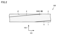
- FIG. 2 is a schematic cross-sectional view taken along line II-II in FIG. 1.
- the cross section shown in FIG. 2 is perpendicular to the first main surface 1 and parallel to the first direction 101.
- silicon carbide substrate 100 according to this embodiment has first main surface 1.
- the first main surface 1 is on the opposite side of the second main surface 2.
- the thickness of silicon carbide substrate 100 is, for example, 300 ⁇ m or more and 700 ⁇ m or less.
- the third direction 103 is a direction perpendicular to each of the first direction 101 and the second direction 102.
- the thickness direction of silicon carbide substrate 100 is the same as third direction 103.
- the off angle ⁇ of the plane inclined in the off direction with respect to the ⁇ 0001 ⁇ plane may be 8° or less.
- the upper limit of the off-angle ⁇ is not particularly limited, but may be, for example, 6° or less, or 4° or less.
- the lower limit of the off-angle ⁇ is not particularly limited, but may be, for example, 1° or more, or 2° or more.
- the off-direction of the plane inclined in the off-direction with respect to the ⁇ 0001 ⁇ plane is, for example, the ⁇ 11-20> direction, although it is not particularly limited.
- silicon carbide substrate 100 has a plurality of basal plane dislocations 4.
- Each of the plurality of basal plane dislocations 4 extends along the (0001) plane.
- basal plane dislocations exposed on first principal surface 1 or second principal surface 2 can be represented as the areal density of basal plane dislocations of silicon carbide substrate 100.
- the areal density of basal plane dislocations 4 is determined using, for example, molten potassium hydroxide (KOH). Specifically, the surface to be measured (for example, the (0001) surface) is etched with molten KOH. As a result, the silicon carbide region near the basal plane dislocations exposed on the surface to be measured is etched, and etch pits are formed on the surface to be measured.
- the temperature of the KOH melt is, for example, 500°C or more and 550°C or less. Etching time is 5 minutes or more and 10 minutes or less.
- etch pits on the surface to be measured are observed using a Normarski differential interference microscope.
- the value obtained by dividing the number of etch pits formed on the surface to be measured by the measurement area on the surface to be measured corresponds to the areal density of basal plane dislocations.
- the observation field of view is, for example, 0.082 cm x 0.070 cm.
- the measurement interval is, for example, 5 mm.
- the areal density of basal plane dislocations 4 on second main surface 2 is 700 cm -2 or more.
- the lower limit of the areal density of basal plane dislocations 4 on the second main surface 2 is not particularly limited, but may be, for example, 800 cm -2 or more, 1000 cm -2 or more, or 1100 cm -2 or more. There may be.
- the upper limit of the areal density of basal plane dislocations 4 on the second principal surface 2 is not particularly limited, but may be, for example, 2000 cm -2 or less, 1500 cm -2 or less, or 1300 cm -2 or less. There may be.
- the areal density of basal plane dislocations 4 on first main surface 1 may be 700 cm ⁇ 2 or more.
- the lower limit of the areal density of basal plane dislocations 4 on the first principal surface 1 is not particularly limited, but may be, for example, 800 cm -2 or more, 1000 cm -2 or more, or 1100 cm -2 or more. There may be.
- the upper limit of the areal density of basal plane dislocations 4 on the first principal surface 1 is not particularly limited, but may be, for example, 2000 cm -2 or less, 1500 cm -2 or less, or 1300 cm -2 or less. There may be.
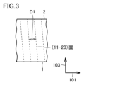
- FIG. 3 is a schematic cross-sectional view taken along line III-III in FIG. 1.
- the area shown in FIG. 3 corresponds to the outer circumference 20.
- the lattice spacing of the (11-20) plane in the outer peripheral portion 20 is a first lattice spacing D1.
- the first lattice spacing D1 corresponds to the lattice constant in the ⁇ 11-20> direction in the outer peripheral portion 20.
- FIG. 4 is a schematic cross-sectional view taken along line IV-IV in FIG. 1.
- the area shown in FIG. 4 corresponds to the central portion 30.
- the lattice spacing of the (11-20) plane in the central portion 30 is the second lattice spacing D2.
- the second lattice spacing D2 corresponds to the lattice constant in the ⁇ 11-20> direction in the central portion 30.
- the lattice spacing in each of the central portion 30 and the outer peripheral portion 20 can be measured using an X-ray diffraction device (product name: SmartLab) manufactured by Rigaku Corporation.
- the X-ray source is, for example, Cu-K ⁇ 1 ray.
- the tube voltage is, for example, 45 kV.
- the tube current is, for example, 40 mA.
- a 2 ⁇ / ⁇ scanning method on a diffraction surface is used.
- the diffraction plane is the (11-20) plane.
- the value obtained by subtracting the lattice spacing of the (11-20) plane in the central portion 30 from the lattice spacing of the (11-20) plane in the outer peripheral portion 20 is as follows: -0.00081 nm or more and 0.00065 nm or less.
- the value obtained by subtracting the lattice spacing of the (11-20) plane in the central portion 30 from the lattice spacing of the (11-20) plane in the outer peripheral portion 20 may be ⁇ 0.00081 nm or more and less than 0 nm.
- the value obtained by subtracting the lattice spacing of the (11-20) plane in the central portion 30 from the lattice spacing of the (11-20) plane in the outer peripheral portion 20 is not particularly limited, but is, for example, -0.00054 nm or more -0. 00017 nm or less, -0.00081 nm or more and -0.00017 nm or less, -0.00054 nm or more and 0.00065 nm or less, or -0.00049 nm or more -0. It may be less than 00022 nm.
- Silicon carbide substrate 100 according to the second embodiment differs from silicon carbide substrate 100 according to the first embodiment in the combination of the areal density of basal plane dislocations 4 and the difference in the lattice spacing of the (11-20) plane.
- the other configurations are substantially the same as silicon carbide substrate 100 according to the first embodiment.
- the structure different from silicon carbide substrate 100 according to the first embodiment will be mainly explained.
- the areal density of basal plane dislocations 4 on second main surface 2 is less than 700 cm ⁇ 2 .
- the lower limit of the areal density of basal plane dislocations 4 on the second main surface 2 is not particularly limited, but may be, for example, 100 cm -2 or more, 200 cm -2 or more, or 250 cm -2 or more. There may be.
- the upper limit of the areal density of basal plane dislocations 4 on the second main surface 2 is not particularly limited, but may be, for example, 500 cm -2 or less, 400 cm -2 or less, or 300 cm -2 or less. There may be.
- the areal density of basal plane dislocations 4 on first main surface 1 is less than 700 cm ⁇ 2 .
- the lower limit of the areal density of basal plane dislocations 4 on the first principal surface 1 is not particularly limited, but may be, for example, 100 cm -2 or more, 200 cm -2 or more, or 250 cm -2 or more. There may be.
- the upper limit of the areal density of basal plane dislocations 4 on the first principal surface 1 is not particularly limited, but may be, for example, 500 cm -2 or less, 400 cm -2 or less, or 300 cm -2 or less. There may be.
- the value obtained by subtracting the lattice spacing of the (11-20) plane in the central portion 30 from the lattice spacing of the (11-20) plane in the outer peripheral portion 20 is as follows: -0.00083 nm or more and -0.00009 nm or less. Even if the value obtained by subtracting the lattice spacing of the (11-20) plane in the central part 30 from the lattice spacing of the (11-20) plane in the outer peripheral part 20 is -0.00083 nm or more and -0.00019 nm or less good.
- the value obtained by subtracting the lattice spacing of the (11-20) plane in the central portion 30 from the lattice spacing of the (11-20) plane in the outer peripheral portion 20 is not particularly limited, but is, for example, -0.00083 nm or more -0. 00024 nm or less, -0.00056 nm or more and -0.00009 nm or less, -0.00056 nm or more and -0.00024 nm or less, or -0.00051 nm or more -0 It may be .00029 nm or less.
- FIG. 5 is a schematic partial cross-sectional view showing the configuration of an apparatus for manufacturing silicon carbide crystal 110 according to the present embodiment.
- an apparatus 300 for manufacturing silicon carbide crystal 110 mainly includes a first crucible 130, a first heat insulating material 145, and an induction heating coil 140.
- the first crucible 130 is made of graphite.
- the first crucible 130 has a first housing section 132 and a first lid section 131.
- the first lid part 131 is arranged on the first accommodating part 132.
- the first heat insulating material 145 is arranged to cover the entire first crucible 130.
- the induction heating coil 140 is arranged in a spiral around the outer periphery of the first heat insulating material 145 . By applying electric power to the induction heating coil 140, the first crucible 130 is heated by electromagnetic induction.
- silicon carbide raw material 153 is placed in first storage portion 132.
- Silicon carbide raw material 153 is, for example, polycrystalline silicon carbide powder.
- the seed substrate 150 is fixed to the first lid part 131 using, for example, an adhesive (not shown).
- Seed substrate 150 has a growth surface 151 and a mounting surface 152. Attachment surface 152 is on the opposite side from growth surface 151. Growth surface 151 faces silicon carbide raw material 153.
- the mounting surface 152 faces the first lid portion 131 . Growth surface 151 of seed substrate 150 is arranged to face the surface of silicon carbide raw material 153.
- Seed substrate 150 is, for example, a silicon carbide single crystal substrate whose polytype is 4H.
- the diameter of the growth surface 151 is, for example, 150 mm.
- the diameter of the growth surface 151 may be 150 mm or more.
- the growth surface 151 is, for example, a surface inclined by an off-angle of about 8° or less with respect to the ⁇ 0001 ⁇ plane. As described above, seed substrate 150 and silicon carbide raw material 153 are placed in first crucible 130.
- FIG. 6 is a schematic cross-sectional view showing the growth process of silicon carbide crystal 110.
- the pressure in first crucible 130 is reduced while the temperature of growth surface 151 of seed substrate 150 is lower than the temperature of silicon carbide raw material 153.
- the pressure of the atmospheric gas in the first crucible 130 is reduced to, for example, 1.0 kPa.
- silicon carbide raw material 153 starts to sublimate, and the sublimated silicon carbide gas recrystallizes on growth surface 151 of seed substrate 150 .
- silicon carbide crystal 110 grows as a single crystal. While silicon carbide crystal 110 is growing, the pressure within first crucible 130 is maintained at, for example, approximately 0.1 kPa or more and 3 kPa or less.
- silicon carbide crystal 110 is grown on seed substrate 150 by subliming silicon carbide raw material 153.
- the temperature of silicon carbide crystal 110 is, for example, 2100° C. or higher and 2300° C. or lower.
- the lower limit of the temperature of silicon carbide crystal 110 is not particularly limited, but may be, for example, 2125° C. or higher, or 2150° C. or higher.
- the upper limit of the temperature of silicon carbide crystal 110 is not particularly limited, but may be, for example, 2250° C. or lower or 2275° C. or lower.
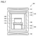
- FIG. 7 is a schematic cross-sectional view showing a step of annealing silicon carbide crystal 110.
- an annealing device 301 for silicon carbide crystal 110 includes a second crucible 135, an upper resistance heater 141, a lower resistance heater 142, a second heat insulating material 146, a support base 160, and a third It mainly has a heat insulating material 170.
- the second crucible 135 is made of graphite.
- the second crucible 135 has a second housing section 134 and a second lid section 133.
- the second lid part 133 is arranged on the second accommodating part 134.
- the second heat insulating material 146 is arranged around the outer peripheral surface of the second crucible 135.
- the second heat insulating material 146 is not arranged at a position facing each of the upper surface and the lower surface of the second crucible 135.
- Upper resistance heater 141 faces the upper surface of second crucible 135 .
- Lower resistance heater 142 faces the lower surface of second crucible 135 .
- the support stand 160 is arranged inside the second accommodating part 134 .
- the support stand 160 has a plate portion 162 and a support portion 161.
- the plate portion 162 is arranged on the support portion 161.
- the third heat insulating material 170 is arranged on the plate portion 162.
- the bulk density of graphite constituting the third heat insulating material 170 is, for example, 0.1 g/cm 3 or more and 0.16 g/cm 3 or less.
- the bulk density of the graphite constituting the support base 160 is, for example, 1.6 g/cm 3 or more and 1.9 g/cm 3 or less.
- Silicon carbide crystal 110 is placed on third heat insulating material 170 . Silicon carbide crystal 110 is in contact with third heat insulating material 170 .
- silicon carbide crystal 110 is heated. No resistance heater is arranged around the outer peripheral surface of silicon carbide crystal 110.
- the thickness of the second heat insulating material 146 is reduced, heat easily escapes from the inside of the second crucible 135 to the outside. Thereby, the difference in temperature between the outer peripheral portion of silicon carbide crystal 110 and the temperature at the central portion of silicon carbide crystal 110 can be reduced.
- the temperature at the outer periphery of silicon carbide crystal 110 may be lower than the temperature at the center of silicon carbide crystal 110.
- silicon carbide crystal 110 is removed from first crucible 130 , it is placed on third heat insulating material 170 in second crucible 135 . Silicon carbide crystal 110 is annealed with silicon carbide crystal 110 disposed on third heat insulating material 170 .
- the difference in coefficient of thermal expansion between silicon carbide crystal 110 and third heat insulating material 170 is smaller than the difference in coefficient of thermal expansion between silicon carbide crystal 110 and first crucible 130 . Therefore, compared to the case where silicon carbide crystal 110 is annealed with silicon carbide crystal 110 attached to first crucible 130, silicon carbide crystal 110 is annealed with silicon carbide crystal 110 disposed on third heat insulating material 170.
- stress in silicon carbide crystal 110 can be effectively alleviated. Thereby, stress in the outer peripheral portion of silicon carbide crystal 110 can be reduced.
- silicon carbide crystal 110 is sliced. Specifically, silicon carbide crystal 110 is sliced along a plane perpendicular to the central axis of silicon carbide crystal 110 using, for example, a saw wire. Thereby, a plurality of silicon carbide substrates 100 according to this embodiment are obtained (see FIG. 2). According to silicon carbide substrate 100 according to the present embodiment, the value obtained by subtracting second lattice spacing D2 from first lattice spacing D1 is a small or negative value.
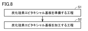
- FIG. 8 is a flowchart schematically showing a method for manufacturing silicon carbide semiconductor device 400 according to this embodiment.
- the method for manufacturing silicon carbide semiconductor device 400 according to the present embodiment includes a step of preparing silicon carbide epitaxial substrate 200 (S1), and a step of processing silicon carbide epitaxial substrate 200 (S2). It mainly has
- a step (S1) of preparing silicon carbide epitaxial substrate 200 is performed.
- silicon carbide substrate 100 according to the first embodiment is prepared (see FIG. 1).
- silicon carbide epitaxial layer 60 is formed on silicon carbide substrate 100.
- silicon carbide epitaxial layer 60 is formed on first main surface 1 of silicon carbide substrate 100 by epitaxial growth.
- silane (SiH 4 ) and propane (C 3 H 8 ) are used as source gases, and hydrogen (H 2 ) is used as a carrier gas.
- the temperature for epitaxial growth is, for example, about 1400° C. or more and 1700° C. or less.
- an n-type impurity, such as nitrogen, is introduced into silicon carbide epitaxial layer 60.
- FIG. 9 is a schematic cross-sectional view showing the configuration of silicon carbide epitaxial substrate 200 according to this embodiment.
- the basal plane dislocation 4 is omitted in the drawings from FIG. 9 onwards.
- silicon carbide epitaxial substrate 200 includes silicon carbide substrate 100 and silicon carbide epitaxial layer 60. Silicon carbide epitaxial layer 60 is provided on silicon carbide substrate 100. Silicon carbide epitaxial layer 60 has third main surface 3 . Third main surface 3 constitutes the surface of silicon carbide epitaxial substrate 200 . Second main surface 2 constitutes the back surface of silicon carbide epitaxial substrate 200 .
- Silicon carbide epitaxial layer 60 may include buffer layer 41 and drift layer 42 .
- Buffer layer 41 is in contact with silicon carbide substrate 100 at first main surface 1 .
- Drift layer 42 is provided on buffer layer 41.
- Each of the buffer layer 41 and the drift layer 42 contains an n-type impurity such as nitrogen.
- the concentration of n-type impurities contained in the buffer layer 41 may be higher than the concentration of n-type impurities contained in the drift layer 42.
- a step (S2) of processing silicon carbide epitaxial substrate 200 is performed. Specifically, the following processing is performed on silicon carbide epitaxial substrate 200. First, ion implantation is performed into silicon carbide epitaxial substrate 200.
- FIG. 10 is a schematic cross-sectional view showing the process of forming the body region.
- a p-type impurity such as aluminum is ion-implanted into third main surface 3 of silicon carbide epitaxial layer 60 .
- body region 113 having p-type conductivity is formed.
- the portion where body region 113 is not formed becomes drift layer 42 and buffer layer 41.
- the thickness of the body region 113 is, for example, 0.9 ⁇ m.
- Silicon carbide epitaxial layer 60 includes buffer layer 41 , drift layer 42 , and body region 113 .
- FIG. 11 is a schematic cross-sectional view showing the process of forming a source region.
- an n-type impurity such as phosphorus is ion-implanted into body region 113, for example.
- a source region 114 having an n-type conductivity type is formed.
- the thickness of the source region 114 is, for example, 0.4 ⁇ m.
- the concentration of n-type impurities contained in source region 114 is higher than the concentration of p-type impurities contained in body region 113.
- a contact region 118 is formed by ion-implanting a p-type impurity such as aluminum into the source region 114.
- Contact region 118 is formed to penetrate source region 114 and body region 113 and be in contact with drift layer 42 .
- the concentration of p-type impurities contained in contact region 118 is higher than the concentration of n-type impurities contained in source region 114.
- activation annealing is performed to activate the ion-implanted impurities.
- the activation annealing temperature is, for example, 1500° C. or more and 1900° C. or less.
- the activation annealing time is, for example, about 30 minutes.
- the activation annealing atmosphere is, for example, an argon atmosphere.
- FIG. 12 is a schematic cross-sectional view showing a step of forming a trench in third main surface 3 of silicon carbide epitaxial layer 60.
- a mask 117 having an opening is formed on the third main surface 3 composed of the source region 114 and the contact region 118. Using mask 117, source region 114, body region 113, and a portion of drift layer 42 are removed by etching.
- the etching method for example, inductively coupled plasma reactive ion etching can be used. Specifically, for example, inductively coupled plasma reactive ion etching using SF 6 or a mixed gas of SF 6 and O 2 as a reactive gas is used. A recess is formed in the third main surface 3 by etching.
- thermal etching is performed in the recesses.
- Thermal etching can be performed, for example, by heating in an atmosphere containing a reactive gas containing at least one type of halogen atom, with the mask 117 formed on the third main surface 3.
- At least one type of halogen atom includes at least one of a chlorine (Cl) atom and a fluorine (F) atom.
- the atmosphere includes, for example, Cl2 , BCl3 , SF6 or CF4 .
- thermal etching is performed using a mixed gas of chlorine gas and oxygen gas as a reaction gas, and at a heat treatment temperature of, for example, 700° C. or higher and 1000° C. or lower.
- the reaction gas may contain a carrier gas in addition to the above-mentioned chlorine gas and oxygen gas.
- the carrier gas for example, nitrogen gas, argon gas, or helium gas can be used.
- trenches 56 are formed in the third main surface 3 by thermal etching.
- Trench 56 is defined by side wall surface 53 and bottom wall surface 54 .
- Sidewall surface 53 is composed of source region 114, body region 113, and drift layer 42.
- the bottom wall surface 54 is composed of the drift layer 42.
- the mask 117 is removed from the third main surface 3.
- FIG. 13 is a schematic cross-sectional view showing the process of forming a gate insulating film.
- silicon carbide epitaxial substrate 200 in which trenches 56 are formed in third main surface 3 is heated at a temperature of, for example, 1300° C. or more and 1400° C. or less in an atmosphere containing oxygen.
- the bottom wall surface 54 is in contact with the drift layer 42
- the side wall surface 53 is in contact with each of the drift layer 42 , the body region 113 , and the source region 114
- the third main surface 3 is in contact with each of the source region 114 and the contact region 118 .
- a contacting gate insulating film 115 is formed.
- FIG. 14 is a schematic cross-sectional view showing the process of forming a gate electrode and an interlayer insulating film.
- Gate electrode 127 is formed inside trench 56 so as to be in contact with gate insulating film 115 .
- Gate electrode 127 is disposed inside trench 56 and formed on gate insulating film 115 so as to face each of side wall surface 53 and bottom wall surface 54 of trench 56 .
- the gate electrode 127 is formed, for example, by LPCVD (Low Pressure Chemical Vapor Deposition) method.
- Interlayer insulating film 126 is formed. Interlayer insulating film 126 is formed to cover gate electrode 127 and to be in contact with gate insulating film 115 .
- the interlayer insulating film 126 is formed, for example, by chemical vapor deposition.
- the interlayer insulating film 126 is made of, for example, a material containing silicon dioxide.
- interlayer insulating film 126 and a portion of gate insulating film 115 are etched so that openings are formed over source region 114 and contact region 118. As a result, contact region 118 and source region 114 are exposed from gate insulating film 115.
- Source electrode 116 is formed so as to be in contact with each of source region 114 and contact region 118.
- Source electrode 116 is formed by, for example, a sputtering method.
- the source electrode 116 is made of a material containing, for example, Ti (titanium), Al (aluminum), and Si (silicon).
- alloying annealing is performed. Specifically, the source electrode 116 in contact with each of the source region 114 and the contact region 118 is maintained at a temperature of, for example, 900° C. or more and 1100° C. or less for about 5 minutes. As a result, at least a portion of the source electrode 116 is silicided. As a result, a source electrode 116 that is in ohmic contact with the source region 114 is formed. Source electrode 116 may be in ohmic contact with contact region 118.
- Source wiring 119 is formed.
- Source wiring 119 is electrically connected to source electrode 116.
- Source wiring 119 is formed to cover source electrode 116 and interlayer insulating film 126 .
- a step of forming a drain electrode is performed. First, silicon carbide substrate 100 is polished on second main surface 2 . This reduces the thickness of silicon carbide substrate 100. Next, drain electrode 123 is formed. Drain electrode 123 is formed so as to be in contact with second main surface 2 . Through the above steps, silicon carbide semiconductor device 400 according to this embodiment is manufactured.
- FIG. 15 is a schematic cross-sectional view showing the configuration of silicon carbide semiconductor device 400 according to this embodiment.
- Silicon carbide semiconductor device 400 is, for example, a MOSFET (Metal Oxide Semiconductor Field Effect Transistor).
- Silicon carbide semiconductor device 400 mainly includes silicon carbide epitaxial substrate 200, gate electrode 127, gate insulating film 115, source electrode 116, drain electrode 123, source wiring 119, and interlayer insulating film 126. ing.
- Silicon carbide epitaxial substrate 200 has buffer layer 41 , drift layer 42 , body region 113 , source region 114 , and contact region 118 .
- Silicon carbide semiconductor device 400 may be, for example, an IGBT (Insulated Gate Bipolar Transistor).
- the outer periphery of the crucible is heated using a heater placed on the outer periphery side of the crucible. Therefore, during crystal growth of silicon carbide crystal 110, the temperature of the outer peripheral portion of silicon carbide crystal 110 is higher than the temperature of the central portion of silicon carbide crystal 110. As a result, compressive stress is generated at the outer periphery of silicon carbide crystal 110.
- silicon carbide substrate 100 includes basal plane dislocations 4
- stress in silicon carbide substrate 100 can be alleviated by movement of basal plane dislocations 4 during the heating process when manufacturing silicon carbide semiconductor device 400. I can do it. Therefore, when the stress of silicon carbide substrate 100 is high, it is desirable that the areal density of basal plane dislocations 4 is high to some extent. On the other hand, if the areal density of basal plane dislocations 4 is excessively high, the reliability of silicon carbide semiconductor device 400 decreases. Therefore, when the stress of silicon carbide substrate 100 is low, it is desirable that the areal density of basal plane dislocations 4 is low to some extent.
- main surface 2 includes central portion 30 and outer peripheral portion 20 located 10 mm away from outer peripheral edge 9 of main surface 2 toward central portion 30. There is.
- the value obtained by subtracting the lattice spacing of the (11-20) plane in the central portion 30 from the lattice spacing of the (11-20) plane in the outer peripheral portion 20 is ⁇ 0.00081 nm or more and 0.00065 nm or less.
- the surface density of basal plane dislocations 4 on the main surface 2 is 700 cm ⁇ 2 or more.
- the basal plane dislocation 4 Since the areal density of silicon carbide substrate 100 is high, stress in silicon carbide substrate 100 can be reduced. Therefore, generation of cracks in silicon carbide substrate 100 can be suppressed.
- the areal density of basal plane dislocations 4 on main surface 2 may be 1000 cm -2 or more. Thereby, generation of cracks in silicon carbide substrate 100 can be further suppressed.
- the value obtained by subtracting the lattice spacing of the (11-20) plane in the central portion 30 from the lattice spacing of the (11-20) plane in the outer peripheral portion 20 is - It may be 0.00054 nm or more and 0.00017 nm or less. Thereby, generation of cracks in silicon carbide substrate 100 can be further suppressed.
- main surface 2 includes central portion 30 and outer peripheral portion 20 located 10 mm away from outer peripheral edge 9 of main surface 2 toward central portion 30. There is.
- the value obtained by subtracting the lattice spacing of the (11-20) plane in the central portion 30 from the lattice spacing of the (11-20) plane in the outer peripheral portion 20 is ⁇ 0.00083 nm or more and ⁇ 0.00009 nm or less.
- the surface density of basal plane dislocations 4 on the main surface 2 is less than 700 cm ⁇ 2 .
- the stress in the silicon carbide substrate 100 can be reduced. can be reduced. Therefore, while suppressing the occurrence of cracks in silicon carbide substrate 100, it is possible to suppress a decrease in reliability of silicon carbide semiconductor device 400.
- the areal density of basal plane dislocations 4 on main surface 2 may be 300 cm ⁇ 2 or less. Thereby, while suppressing the occurrence of cracks in silicon carbide substrate 100, it is possible to further suppress a decrease in reliability of silicon carbide semiconductor device 400.
- the value obtained by subtracting the lattice spacing of the (11-20) plane in the central portion 30 from the lattice spacing of the (11-20) plane in the outer peripheral portion 20 is - It may be 0.00056 nm or more and 0.00024 nm or less.
- main surface 2 When the diameter of main surface 2 is large, the temperature difference between central portion 30 and outer peripheral portion 20 becomes large, making silicon carbide substrate 100 more likely to crack.
- main surface 2 may have a diameter of 150 mm or more. When the diameter of main surface 2 is large, it is possible to effectively suppress the occurrence of cracks in silicon carbide substrate 100.
- the diameter of main surface 2 may be 200 mm or more.
- the diameter of main surface 2 is large, it is possible to effectively suppress the occurrence of cracks in silicon carbide substrate 100.
- silicon carbide crystal 110 was manufactured using manufacturing conditions related to Samples 1 to 8. Under the manufacturing conditions for Samples 1 to 8, a step of growing silicon carbide crystal 110 by a sublimation method was performed. Specifically, silicon carbide crystal 110 was manufactured using the first crucible shown in FIG.
- the annealing process for silicon carbide crystal 110 was not performed after the silicon carbide crystal 110 growth process. Under the manufacturing conditions for Samples 3 to 8, the annealing process for silicon carbide crystal 110 was performed after the silicon carbide crystal 110 growth process. Specifically, an annealing process for silicon carbide crystal 110 was performed using annealing apparatus 301 shown in FIG.
- the temperature of central portion 30 of silicon carbide crystal 110 was 2200°C.
- the pressure inside the annealing device 301 was 90 kPa.
- the atmosphere gas was argon gas.
- the annealing time was 5 hours.
- silicon carbide crystal 110 was sliced using a saw wire. As a result, three silicon carbide substrates 100 were cut out. Each of three silicon carbide substrates 100 has a first main surface 1 and a second main surface 2.
- the second principal surface 2 was a surface inclined in the off direction with respect to the ⁇ 0001 ⁇ plane.
- the off direction was set to ⁇ 11-20>.
- the off angle ⁇ was 4°.
- silicon carbide substrates 100 manufactured using the manufacturing conditions of each of Samples 1 to 8 were prepared.
- the lattice spacing in each of the central portion 30 and outer peripheral portion 20 of the second principal surface 2 was measured using an X-ray diffraction device (product name: SmartLab) manufactured by Rigaku Co., Ltd.
- the X-ray source was Cu-K ⁇ 1 ray.
- the tube voltage was 45 kV.
- the tube current was 40 mA.
- a 2 ⁇ / ⁇ scanning method on a diffraction surface was used.
- the diffraction plane was the (11-20) plane.
- the value obtained by subtracting the lattice spacing of the (11-20) plane in the central part 30 from the lattice spacing of the (11-20) plane in the outer peripheral part 20 is taken as the difference in the lattice spacing of the (11-20) plane. .
- the areal density of basal plane dislocations 4 was determined using molten potassium hydroxide (KOH).
- KOH molten potassium hydroxide
- the temperature of the KOH melt was 500°C or more and 550°C or less.
- the etching time was 5 minutes or more and 10 minutes or less.
- etch pits on the surface to be measured were observed using a Normarski differential interference microscope.
- the observation field was 0.082 cm x 0.070 cm.
- the measurement interval was 5 mm.
- Table 1 shows the difference in the lattice spacing of the (11-20) plane in the silicon carbide substrates 100 of each of Samples 1 to 8, the areal density of basal plane dislocations 4 in the second principal surface 2, and the presence or absence of cracks. It shows.
- a silicon carbide substrate having a main surface having a main surface, The main surface includes a central part and an outer peripheral part located 10 mm away from the outer peripheral edge of the main surface toward the central part, The value obtained by subtracting the lattice spacing of the (11-20) plane in the central portion from the lattice spacing of the (11-20) plane in the outer peripheral portion is ⁇ 0.00081 nm or more and 0.00065 nm or less,
- the silicon carbide substrate has a surface density of basal plane dislocations on the main surface of 700 cm -2 or more.
- the silicon carbide substrate according to Supplementary Note 1 wherein the surface density of basal plane dislocations on the main surface is 1000 cm -2 or more.
- (Appendix 9) The silicon carbide substrate according to any one of Supplementary notes 1 to 8, wherein the main surface has a diameter of 150 mm or more.
- (Appendix 10) The silicon carbide substrate according to appendix 9, wherein the main surface has a diameter of 200 mm or more.
- (Appendix 11) The silicon carbide substrate according to any one of Supplementary notes 1 to 8, A silicon carbide epitaxial substrate, comprising: a silicon carbide epitaxial layer provided on the silicon carbide substrate.
- (Appendix 12) A step of preparing a silicon carbide epitaxial substrate according to Appendix 11; A method for manufacturing a silicon carbide semiconductor device, comprising the step of processing the silicon carbide epitaxial substrate.
Landscapes
- Chemical & Material Sciences (AREA)
- Engineering & Computer Science (AREA)
- Crystallography & Structural Chemistry (AREA)
- Materials Engineering (AREA)
- Metallurgy (AREA)
- Organic Chemistry (AREA)
- Chemical Kinetics & Catalysis (AREA)
- General Chemical & Material Sciences (AREA)
- Inorganic Chemistry (AREA)
- Crystals, And After-Treatments Of Crystals (AREA)
Priority Applications (1)
| Application Number | Priority Date | Filing Date | Title |
|---|---|---|---|
| JP2024533659A JPWO2024014358A1 (https=) | 2022-07-14 | 2023-07-04 |
Applications Claiming Priority (2)
| Application Number | Priority Date | Filing Date | Title |
|---|---|---|---|
| JP2022113414 | 2022-07-14 | ||
| JP2022-113414 | 2022-07-14 |
Publications (1)
| Publication Number | Publication Date |
|---|---|
| WO2024014358A1 true WO2024014358A1 (ja) | 2024-01-18 |
Family
ID=89536622
Family Applications (1)
| Application Number | Title | Priority Date | Filing Date |
|---|---|---|---|
| PCT/JP2023/024796 Ceased WO2024014358A1 (ja) | 2022-07-14 | 2023-07-04 | 炭化珪素基板、炭化珪素エピタキシャル基板および炭化珪素半導体装置の製造方法 |
Country Status (2)
| Country | Link |
|---|---|
| JP (1) | JPWO2024014358A1 (https=) |
| WO (1) | WO2024014358A1 (https=) |
Citations (1)
| Publication number | Priority date | Publication date | Assignee | Title |
|---|---|---|---|---|
| JP2018140903A (ja) * | 2017-02-28 | 2018-09-13 | 昭和電工株式会社 | 炭化珪素単結晶インゴットの製造方法 |
-
2023
- 2023-07-04 WO PCT/JP2023/024796 patent/WO2024014358A1/ja not_active Ceased
- 2023-07-04 JP JP2024533659A patent/JPWO2024014358A1/ja active Pending
Patent Citations (1)
| Publication number | Priority date | Publication date | Assignee | Title |
|---|---|---|---|---|
| JP2018140903A (ja) * | 2017-02-28 | 2018-09-13 | 昭和電工株式会社 | 炭化珪素単結晶インゴットの製造方法 |
Also Published As
| Publication number | Publication date |
|---|---|
| JPWO2024014358A1 (https=) | 2024-01-18 |
Similar Documents
| Publication | Publication Date | Title |
|---|---|---|
| US9915011B2 (en) | Low resistivity single crystal silicon carbide wafer | |
| JP5068423B2 (ja) | 炭化珪素単結晶インゴット、炭化珪素単結晶ウェハ及びその製造方法 | |
| JP6508050B2 (ja) | 炭化珪素インゴットの製造方法、炭化珪素基板の製造方法、および半導体装置の製造方法 | |
| JP6183010B2 (ja) | 炭化珪素単結晶基板およびその製造方法 | |
| US9966249B2 (en) | Silicon carbide semiconductor substrate and method for manufacturing same | |
| US9728628B2 (en) | Silicon carbide semiconductor device and method for manufacturing same | |
| US20220282395A1 (en) | SiC SUBSTRATE, SiC EPITAXIAL SUBSTRATE, SiC INGOT AND PRODUCTION METHODS THEREOF | |
| JP2020142985A (ja) | 炭化珪素エピタキシャル基板および炭化珪素半導体装置の製造方法 | |
| CN110214363A (zh) | 碳化硅外延衬底和制造碳化硅半导体器件的方法 | |
| EP4105367A1 (en) | Silicon carbide wafer and semiconductor device | |
| JP7415558B2 (ja) | 炭化珪素エピタキシャル基板および炭化珪素半導体装置の製造方法 | |
| US20240332364A1 (en) | Silicon carbide epitaxial substrate, method of manufacturing silicon carbide epitaxial substrate, and method of manufacturing silicon carbide semiconductor device | |
| US20250203985A1 (en) | Silicon carbide substrate, silicon carbide epitaxial substrate, and method of manufacturing silicon carbide semiconductor device | |
| WO2024084910A1 (ja) | 炭化珪素基板、炭化珪素エピタキシャル基板の製造方法および炭化珪素半導体装置の製造方法 | |
| WO2024014358A1 (ja) | 炭化珪素基板、炭化珪素エピタキシャル基板および炭化珪素半導体装置の製造方法 | |
| US20260082649A1 (en) | Silicon carbide epitaxial substrate, method of manufacturing epitaxial substrate, and method of manufacturing silicon carbide semiconductor device | |
| JP6748613B2 (ja) | 炭化珪素単結晶基板 | |
| US20250056856A1 (en) | Silicon carbide substrate, method of manufacturing silicon carbide semiconductor device, and method of manufacturing silicon carbide substrate | |
| JP2003137694A (ja) | 炭化珪素単結晶育成用種結晶と炭化珪素単結晶インゴット及びその製造方法 | |
| WO2025134535A1 (ja) | 炭化珪素基板、炭化珪素エピタキシャル基板の製造方法、および炭化珪素半導体装置の製造方法 | |
| JP2025139953A (ja) | 炭化珪素基板、炭化珪素基板の製造方法、炭化珪素エピタキシャル基板の製造方法、炭化珪素エピタキシャル基板、炭化珪素半導体装置の製造方法、および炭化珪素半導体装置 | |
| JP7661771B2 (ja) | 炭化珪素エピタキシャル基板の製造方法および炭化珪素半導体装置の製造方法 | |
| US20250393275A1 (en) | Silicon carbide epitaxial substrate and method of manufacturing silicon carbide semiconductor device | |
| JP2025136294A (ja) | 炭化珪素基板、炭化珪素エピタキシャル基板、炭化珪素半導体装置の製造方法、および炭化珪素結晶の製造方法 | |
| WO2024048157A1 (ja) | 炭化珪素基板、炭化珪素基板の製造方法、炭化珪素単結晶の製造方法、エピタキシャル基板および半導体装置の製造方法 |
Legal Events
| Date | Code | Title | Description |
|---|---|---|---|
| 121 | Ep: the epo has been informed by wipo that ep was designated in this application |
Ref document number: 23839530 Country of ref document: EP Kind code of ref document: A1 |
|
| WWE | Wipo information: entry into national phase |
Ref document number: 2024533659 Country of ref document: JP |
|
| NENP | Non-entry into the national phase |
Ref country code: DE |
|
| 122 | Ep: pct application non-entry in european phase |
Ref document number: 23839530 Country of ref document: EP Kind code of ref document: A1 |