WO2024014342A1 - 接合方法及び接合装置 - Google Patents
接合方法及び接合装置 Download PDFInfo
- Publication number
- WO2024014342A1 WO2024014342A1 PCT/JP2023/024636 JP2023024636W WO2024014342A1 WO 2024014342 A1 WO2024014342 A1 WO 2024014342A1 JP 2023024636 W JP2023024636 W JP 2023024636W WO 2024014342 A1 WO2024014342 A1 WO 2024014342A1
- Authority
- WO
- WIPO (PCT)
- Prior art keywords
- substrate
- ionic liquid
- bonding
- exposed
- joining
- Prior art date
- Legal status (The legal status is an assumption and is not a legal conclusion. Google has not performed a legal analysis and makes no representation as to the accuracy of the status listed.)
- Ceased
Links
Images



Classifications
-
- H—ELECTRICITY
- H10—SEMICONDUCTOR DEVICES; ELECTRIC SOLID-STATE DEVICES NOT OTHERWISE PROVIDED FOR
- H10P—GENERIC PROCESSES OR APPARATUS FOR THE MANUFACTURE OR TREATMENT OF DEVICES COVERED BY CLASS H10
- H10P72/00—Handling or holding of wafers, substrates or devices during manufacture or treatment thereof
-
- B—PERFORMING OPERATIONS; TRANSPORTING
- B29—WORKING OF PLASTICS; WORKING OF SUBSTANCES IN A PLASTIC STATE IN GENERAL
- B29C—SHAPING OR JOINING OF PLASTICS; SHAPING OF MATERIAL IN A PLASTIC STATE, NOT OTHERWISE PROVIDED FOR; AFTER-TREATMENT OF THE SHAPED PRODUCTS, e.g. REPAIRING
- B29C65/00—Joining or sealing of preformed parts, e.g. welding of plastics materials; Apparatus therefor
- B29C65/48—Joining or sealing of preformed parts, e.g. welding of plastics materials; Apparatus therefor using adhesives, i.e. using supplementary joining material; solvent bonding
- B29C65/4855—Joining or sealing of preformed parts, e.g. welding of plastics materials; Apparatus therefor using adhesives, i.e. using supplementary joining material; solvent bonding characterised by their physical properties, e.g. being electrically-conductive
-
- H—ELECTRICITY
- H10—SEMICONDUCTOR DEVICES; ELECTRIC SOLID-STATE DEVICES NOT OTHERWISE PROVIDED FOR
- H10W—GENERIC PACKAGES, INTERCONNECTIONS, CONNECTORS OR OTHER CONSTRUCTIONAL DETAILS OF DEVICES COVERED BY CLASS H10
- H10W72/00—Interconnections or connectors in packages
- H10W72/01—Manufacture or treatment
- H10W72/019—Manufacture or treatment of bond pads
-
- B—PERFORMING OPERATIONS; TRANSPORTING
- B29—WORKING OF PLASTICS; WORKING OF SUBSTANCES IN A PLASTIC STATE IN GENERAL
- B29C—SHAPING OR JOINING OF PLASTICS; SHAPING OF MATERIAL IN A PLASTIC STATE, NOT OTHERWISE PROVIDED FOR; AFTER-TREATMENT OF THE SHAPED PRODUCTS, e.g. REPAIRING
- B29C65/00—Joining or sealing of preformed parts, e.g. welding of plastics materials; Apparatus therefor
- B29C65/48—Joining or sealing of preformed parts, e.g. welding of plastics materials; Apparatus therefor using adhesives, i.e. using supplementary joining material; solvent bonding
- B29C65/4805—Joining or sealing of preformed parts, e.g. welding of plastics materials; Apparatus therefor using adhesives, i.e. using supplementary joining material; solvent bonding characterised by the type of adhesives
- B29C65/483—Reactive adhesives, e.g. chemically curing adhesives
-
- H—ELECTRICITY
- H10—SEMICONDUCTOR DEVICES; ELECTRIC SOLID-STATE DEVICES NOT OTHERWISE PROVIDED FOR
- H10P—GENERIC PROCESSES OR APPARATUS FOR THE MANUFACTURE OR TREATMENT OF DEVICES COVERED BY CLASS H10
- H10P14/00—Formation of materials, e.g. in the shape of layers or pillars
- H10P14/40—Formation of materials, e.g. in the shape of layers or pillars of conductive or resistive materials
-
- H—ELECTRICITY
- H10—SEMICONDUCTOR DEVICES; ELECTRIC SOLID-STATE DEVICES NOT OTHERWISE PROVIDED FOR
- H10P—GENERIC PROCESSES OR APPARATUS FOR THE MANUFACTURE OR TREATMENT OF DEVICES COVERED BY CLASS H10
- H10P72/00—Handling or holding of wafers, substrates or devices during manufacture or treatment thereof
- H10P72/04—Apparatus for manufacture or treatment
- H10P72/0428—Apparatus for mechanical treatment or grinding or cutting
-
- H—ELECTRICITY
- H10—SEMICONDUCTOR DEVICES; ELECTRIC SOLID-STATE DEVICES NOT OTHERWISE PROVIDED FOR
- H10P—GENERIC PROCESSES OR APPARATUS FOR THE MANUFACTURE OR TREATMENT OF DEVICES COVERED BY CLASS H10
- H10P72/00—Handling or holding of wafers, substrates or devices during manufacture or treatment thereof
- H10P72/04—Apparatus for manufacture or treatment
- H10P72/0448—Apparatus for applying a liquid, a resin, an ink or the like
-
- H—ELECTRICITY
- H10—SEMICONDUCTOR DEVICES; ELECTRIC SOLID-STATE DEVICES NOT OTHERWISE PROVIDED FOR
- H10W—GENERIC PACKAGES, INTERCONNECTIONS, CONNECTORS OR OTHER CONSTRUCTIONAL DETAILS OF DEVICES COVERED BY CLASS H10
- H10W20/00—Interconnections in chips, wafers or substrates
- H10W20/01—Manufacture or treatment
-
- H—ELECTRICITY
- H10—SEMICONDUCTOR DEVICES; ELECTRIC SOLID-STATE DEVICES NOT OTHERWISE PROVIDED FOR
- H10W—GENERIC PACKAGES, INTERCONNECTIONS, CONNECTORS OR OTHER CONSTRUCTIONAL DETAILS OF DEVICES COVERED BY CLASS H10
- H10W20/00—Interconnections in chips, wafers or substrates
- H10W20/40—Interconnections external to wafers or substrates, e.g. back-end-of-line [BEOL] metallisations or vias connecting to gate electrodes
-
- H—ELECTRICITY
- H10—SEMICONDUCTOR DEVICES; ELECTRIC SOLID-STATE DEVICES NOT OTHERWISE PROVIDED FOR
- H10W—GENERIC PACKAGES, INTERCONNECTIONS, CONNECTORS OR OTHER CONSTRUCTIONAL DETAILS OF DEVICES COVERED BY CLASS H10
- H10W72/00—Interconnections or connectors in packages
- H10W72/01—Manufacture or treatment
- H10W72/013—Manufacture or treatment of die-attach connectors
-
- H—ELECTRICITY
- H10—SEMICONDUCTOR DEVICES; ELECTRIC SOLID-STATE DEVICES NOT OTHERWISE PROVIDED FOR
- H10W—GENERIC PACKAGES, INTERCONNECTIONS, CONNECTORS OR OTHER CONSTRUCTIONAL DETAILS OF DEVICES COVERED BY CLASS H10
- H10W72/00—Interconnections or connectors in packages
- H10W72/01—Manufacture or treatment
- H10W72/013—Manufacture or treatment of die-attach connectors
- H10W72/01321—Manufacture or treatment of die-attach connectors using local deposition
- H10W72/01323—Manufacture or treatment of die-attach connectors using local deposition in liquid form, e.g. by dispensing droplets or by screen printing
-
- H—ELECTRICITY
- H10—SEMICONDUCTOR DEVICES; ELECTRIC SOLID-STATE DEVICES NOT OTHERWISE PROVIDED FOR
- H10W—GENERIC PACKAGES, INTERCONNECTIONS, CONNECTORS OR OTHER CONSTRUCTIONAL DETAILS OF DEVICES COVERED BY CLASS H10
- H10W72/00—Interconnections or connectors in packages
- H10W72/01—Manufacture or treatment
- H10W72/013—Manufacture or treatment of die-attach connectors
- H10W72/01351—Changing the shapes of die-attach connectors
- H10W72/01353—Changing the shapes of die-attach connectors by etching
-
- H—ELECTRICITY
- H10—SEMICONDUCTOR DEVICES; ELECTRIC SOLID-STATE DEVICES NOT OTHERWISE PROVIDED FOR
- H10W—GENERIC PACKAGES, INTERCONNECTIONS, CONNECTORS OR OTHER CONSTRUCTIONAL DETAILS OF DEVICES COVERED BY CLASS H10
- H10W72/00—Interconnections or connectors in packages
- H10W72/01—Manufacture or treatment
- H10W72/019—Manufacture or treatment of bond pads
- H10W72/01921—Manufacture or treatment of bond pads using local deposition
- H10W72/01923—Manufacture or treatment of bond pads using local deposition in liquid form, e.g. by dispensing droplets or by screen printing
-
- H—ELECTRICITY
- H10—SEMICONDUCTOR DEVICES; ELECTRIC SOLID-STATE DEVICES NOT OTHERWISE PROVIDED FOR
- H10W—GENERIC PACKAGES, INTERCONNECTIONS, CONNECTORS OR OTHER CONSTRUCTIONAL DETAILS OF DEVICES COVERED BY CLASS H10
- H10W72/00—Interconnections or connectors in packages
- H10W72/01—Manufacture or treatment
- H10W72/019—Manufacture or treatment of bond pads
- H10W72/01951—Changing the shapes of bond pads
- H10W72/01953—Changing the shapes of bond pads by etching
-
- H—ELECTRICITY
- H10—SEMICONDUCTOR DEVICES; ELECTRIC SOLID-STATE DEVICES NOT OTHERWISE PROVIDED FOR
- H10W—GENERIC PACKAGES, INTERCONNECTIONS, CONNECTORS OR OTHER CONSTRUCTIONAL DETAILS OF DEVICES COVERED BY CLASS H10
- H10W72/00—Interconnections or connectors in packages
- H10W72/071—Connecting or disconnecting
-
- H—ELECTRICITY
- H10—SEMICONDUCTOR DEVICES; ELECTRIC SOLID-STATE DEVICES NOT OTHERWISE PROVIDED FOR
- H10W—GENERIC PACKAGES, INTERCONNECTIONS, CONNECTORS OR OTHER CONSTRUCTIONAL DETAILS OF DEVICES COVERED BY CLASS H10
- H10W72/00—Interconnections or connectors in packages
- H10W72/071—Connecting or disconnecting
- H10W72/0711—Apparatus therefor
-
- H—ELECTRICITY
- H10—SEMICONDUCTOR DEVICES; ELECTRIC SOLID-STATE DEVICES NOT OTHERWISE PROVIDED FOR
- H10W—GENERIC PACKAGES, INTERCONNECTIONS, CONNECTORS OR OTHER CONSTRUCTIONAL DETAILS OF DEVICES COVERED BY CLASS H10
- H10W72/00—Interconnections or connectors in packages
- H10W72/071—Connecting or disconnecting
- H10W72/0711—Apparatus therefor
- H10W72/07125—Means for controlling the bonding environment, e.g. valves or vacuum pumps
-
- H—ELECTRICITY
- H10—SEMICONDUCTOR DEVICES; ELECTRIC SOLID-STATE DEVICES NOT OTHERWISE PROVIDED FOR
- H10W—GENERIC PACKAGES, INTERCONNECTIONS, CONNECTORS OR OTHER CONSTRUCTIONAL DETAILS OF DEVICES COVERED BY CLASS H10
- H10W72/00—Interconnections or connectors in packages
- H10W72/071—Connecting or disconnecting
- H10W72/0711—Apparatus therefor
- H10W72/07141—Means for applying energy, e.g. ovens or lasers
-
- H—ELECTRICITY
- H10—SEMICONDUCTOR DEVICES; ELECTRIC SOLID-STATE DEVICES NOT OTHERWISE PROVIDED FOR
- H10W—GENERIC PACKAGES, INTERCONNECTIONS, CONNECTORS OR OTHER CONSTRUCTIONAL DETAILS OF DEVICES COVERED BY CLASS H10
- H10W72/00—Interconnections or connectors in packages
- H10W72/071—Connecting or disconnecting
- H10W72/073—Connecting or disconnecting of die-attach connectors
-
- H—ELECTRICITY
- H10—SEMICONDUCTOR DEVICES; ELECTRIC SOLID-STATE DEVICES NOT OTHERWISE PROVIDED FOR
- H10W—GENERIC PACKAGES, INTERCONNECTIONS, CONNECTORS OR OTHER CONSTRUCTIONAL DETAILS OF DEVICES COVERED BY CLASS H10
- H10W72/00—Interconnections or connectors in packages
- H10W72/071—Connecting or disconnecting
- H10W72/073—Connecting or disconnecting of die-attach connectors
- H10W72/07341—Controlling the bonding environment, e.g. atmosphere composition or temperature
-
- H—ELECTRICITY
- H10—SEMICONDUCTOR DEVICES; ELECTRIC SOLID-STATE DEVICES NOT OTHERWISE PROVIDED FOR
- H10W—GENERIC PACKAGES, INTERCONNECTIONS, CONNECTORS OR OTHER CONSTRUCTIONAL DETAILS OF DEVICES COVERED BY CLASS H10
- H10W72/00—Interconnections or connectors in packages
- H10W72/30—Die-attach connectors
-
- H—ELECTRICITY
- H10—SEMICONDUCTOR DEVICES; ELECTRIC SOLID-STATE DEVICES NOT OTHERWISE PROVIDED FOR
- H10W—GENERIC PACKAGES, INTERCONNECTIONS, CONNECTORS OR OTHER CONSTRUCTIONAL DETAILS OF DEVICES COVERED BY CLASS H10
- H10W72/00—Interconnections or connectors in packages
- H10W72/90—Bond pads, in general
-
- H—ELECTRICITY
- H10—SEMICONDUCTOR DEVICES; ELECTRIC SOLID-STATE DEVICES NOT OTHERWISE PROVIDED FOR
- H10W—GENERIC PACKAGES, INTERCONNECTIONS, CONNECTORS OR OTHER CONSTRUCTIONAL DETAILS OF DEVICES COVERED BY CLASS H10
- H10W80/00—Direct bonding of chips, wafers or substrates
- H10W80/102—Controlling the environment during the bonding, e.g. the temperature or pressure
-
- H—ELECTRICITY
- H10—SEMICONDUCTOR DEVICES; ELECTRIC SOLID-STATE DEVICES NOT OTHERWISE PROVIDED FOR
- H10W—GENERIC PACKAGES, INTERCONNECTIONS, CONNECTORS OR OTHER CONSTRUCTIONAL DETAILS OF DEVICES COVERED BY CLASS H10
- H10W90/00—Package configurations
-
- H—ELECTRICITY
- H10—SEMICONDUCTOR DEVICES; ELECTRIC SOLID-STATE DEVICES NOT OTHERWISE PROVIDED FOR
- H10W—GENERIC PACKAGES, INTERCONNECTIONS, CONNECTORS OR OTHER CONSTRUCTIONAL DETAILS OF DEVICES COVERED BY CLASS H10
- H10W80/00—Direct bonding of chips, wafers or substrates
- H10W80/211—Direct bonding of chips, wafers or substrates using auxiliary members, e.g. aids for protecting the bonding area
-
- H—ELECTRICITY
- H10—SEMICONDUCTOR DEVICES; ELECTRIC SOLID-STATE DEVICES NOT OTHERWISE PROVIDED FOR
- H10W—GENERIC PACKAGES, INTERCONNECTIONS, CONNECTORS OR OTHER CONSTRUCTIONAL DETAILS OF DEVICES COVERED BY CLASS H10
- H10W80/00—Direct bonding of chips, wafers or substrates
- H10W80/301—Bonding techniques, e.g. hybrid bonding
- H10W80/312—Bonding techniques, e.g. hybrid bonding characterised by the direct bonding of electrically conductive pads
-
- H—ELECTRICITY
- H10—SEMICONDUCTOR DEVICES; ELECTRIC SOLID-STATE DEVICES NOT OTHERWISE PROVIDED FOR
- H10W—GENERIC PACKAGES, INTERCONNECTIONS, CONNECTORS OR OTHER CONSTRUCTIONAL DETAILS OF DEVICES COVERED BY CLASS H10
- H10W80/00—Direct bonding of chips, wafers or substrates
- H10W80/301—Bonding techniques, e.g. hybrid bonding
- H10W80/327—Bonding techniques, e.g. hybrid bonding characterised by the direct bonding of insulating parts, e.g. of silicon oxide layers
-
- H—ELECTRICITY
- H10—SEMICONDUCTOR DEVICES; ELECTRIC SOLID-STATE DEVICES NOT OTHERWISE PROVIDED FOR
- H10W—GENERIC PACKAGES, INTERCONNECTIONS, CONNECTORS OR OTHER CONSTRUCTIONAL DETAILS OF DEVICES COVERED BY CLASS H10
- H10W90/00—Package configurations
- H10W90/701—Package configurations characterised by the relative positions of pads or connectors relative to package parts
- H10W90/791—Package configurations characterised by the relative positions of pads or connectors relative to package parts of direct-bonded pads
- H10W90/792—Package configurations characterised by the relative positions of pads or connectors relative to package parts of direct-bonded pads between multiple chips
Definitions
- the present disclosure relates to a bonding method and a bonding device.
- Patent Documents 1 and 2 A technique for bonding substrates having an insulating film and a conductive film formed on their surfaces is known (for example, see Patent Documents 1 and 2).
- the present disclosure provides a technology that can suppress oxidation of the bonding surface between substrates.
- a bonding method includes the steps of preparing a first substrate and a second substrate each having a first region where an insulating film is exposed and a second region where a conductive film is exposed on the surfaces thereof; and a step of applying an ionic liquid to the surface of at least one of the second substrates, and a step of bonding the surface of the first substrate and the surface of the second substrate via the ionic liquid.
- oxidation of the bonding surface between substrates can be suppressed.
- FIG. 1 is a flowchart showing a joining method according to an embodiment.
- FIG. 2 is a cross-sectional view showing the joining method according to the embodiment.
- FIG. 3 is a cross-sectional view showing the joining method according to the embodiment.
- FIG. 4 is a cross-sectional view showing the joining method according to the embodiment.
- FIG. 5 is a cross-sectional view showing the joining method according to the embodiment.
- FIG. 6 is a cross-sectional view showing the joining method according to the embodiment.
- FIG. 7 is a cross-sectional view showing the joining method according to the embodiment.
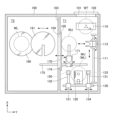
- FIG. 8 is a cross-sectional view showing the joining device according to the embodiment.
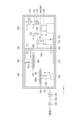
- FIG. 9 is a longitudinal sectional view showing the joining device according to the embodiment.
- two substrates each having different allowable thermal budgets for example, an N-channel (Nch) transistor circuit part of a C-FET (Complementary-Field Effect Transistor) built on a Si substrate and a P-channel (Pch)
- Nch N-channel
- C-FET Complementary-Field Effect Transistor
- Pch P-channel
- One element can be formed by vertically stacking a transistor circuit part or by bonding a Si substrate and a different substrate such as a Ge or III-V group substrate after forming an electronic circuit element. Since hybrid junctions do not require signal communication between low-impedance input/output circuits formed on different substrates, signal transmission between electronic circuit elements formed on substrates can be dramatically speeded up.
- FIG. 1 A joining method according to an embodiment will be described with reference to FIGS. 1 to 7. As shown in FIG. 1, the joining method according to the embodiment includes steps S1 to S3. Steps S1 to S3 are performed in this order.
- step S1 the first substrate 10 and the second substrate 20 are prepared.
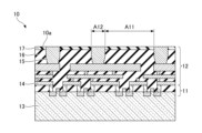
- the first substrate 10 has a calculation section 11 and a wiring layer 12, as shown in FIG.
- the calculation unit 11 is formed including a part of the base substrate 13.
- the calculation unit 11 includes, for example, a semiconductor device such as a transistor.
- the base substrate 13 is, for example, a semiconductor wafer.
- the wiring layer 12 is, for example, a multilayer wiring.
- the wiring layer 12 includes wiring 14 , an electrode pad 15 , a first insulating film 16 , and a second insulating film 17 .
- the wiring 14 is provided in multiple layers.
- the wiring 14 is made of copper (Cu), for example.
- the wiring 14 is electrically connected to the calculation section 11 .
- the electrode pad 15 is provided on the wiring 14 at the farthest position from the base substrate 13. Electrode pad 15 is electrically connected to wiring 14 .
- Electrode pad 15 is electrically connected to calculation unit 11 via wiring 14 .
- the upper surface of the electrode pad 15 is exposed.
- the electrode pad 15 is made of, for example, Cu.
- the first insulating film 16 is, for example, an interlayer insulating film that fills between the wirings 14.
- the interlayer insulating film is preferably a low dielectric constant (Low-k) film.
- the interlayer insulating film is, for example, an SiO film, a SiN film, a SiOC film, a SiON film, or a SiOCN film, although it is not particularly limited.
- the SiO film means a film containing silicon (Si) and oxygen (O).
- the atomic ratio of Si and O in the SiO film is not limited to 1:1. The same applies to the SiN film, SiOC film, SiON film, and SiOCN film.
- the second insulating film 17 is provided on the first insulating film 16. The upper surface of the second insulating film 17 is exposed. The upper surface of the second insulating film 17 is flush with the upper surface of the electrode pad 15, for example.
- the second insulating film 17 may be, for example, an insulating film other than an oxide film.
- the second insulating film 17 is, for example, a SiC film.
- the wiring layer 12 may further include a barrier film between the wiring 14 and the first insulating film 16, for example.
- the wiring layer 12 may further include a barrier film between the electrode pad 15 and the first insulating film 16, for example.
- the barrier film suppresses metal diffusion from the wiring 14 and the electrode pad 15 to the first insulating film 16.
- the barrier film is, for example, a TaN film or a TiN film, although it is not particularly limited.
- the TaN film means a film containing tantalum (Ta) and nitrogen (N).
- the atomic ratio of Ta and N in the TaN film is not limited to 1:1. The same applies to the TiN film.
- the first substrate 10 has a first region A11 where the second insulating film 17 is exposed and a second region A12 where the electrode pad 15 is exposed on the surface 10a.
- the second insulating film 17 is an example of an insulating film
- the electrode pad 15 is an example of a conductive film.
- the second substrate 20 has, for example, substantially the same configuration as the first substrate 10.
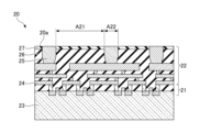
- the second substrate 20 has a calculation section 21 and a wiring layer 22, as shown in FIG.
- the calculation unit 21 is formed including a part of the base substrate 23.
- the wiring layer 22 is, for example, a multilayer wiring.
- the wiring layer 22 includes a wiring 24 , an electrode pad 25 , a first insulating film 26 , and a second insulating film 27 .
- the electrode pad 25 is made of the same material as the electrode pad 15, for example. In this case, even if the electrode pad 15 and the electrode pad 25 come into contact with each other via the ionic liquid in step S3, catalytic corrosion of dissimilar metals (galvanic corrosion) does not occur.
- the second substrate 20 has a first region A21 where the second insulating film 27 is exposed and a second region A22 where the electrode pad 25 is exposed on the surface 20a.
- the second insulating film 27 is an example of an insulating film
- the electrode pad 25 is an example of a conductive film.
- Step S1 may include planarizing the surface 10a of the first substrate 10 and the surface 20a of the second substrate 20 by chemical mechanical polishing (CMP).
- CMP chemical mechanical polishing
- Step S1 may include cleaning the surfaces 10a, 20a with a cleaning liquid after flattening the surfaces 10a, 20a.
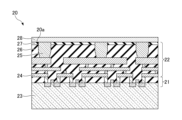
- step S2 as shown in FIG. 4, an ionic liquid is applied to the surface 10a of the first substrate 10.
- the surface 10a of the first substrate 10 is covered with the ionic liquid film 18, so that the exposed surface of the electrode pad 15 can be prevented from being oxidized.
- Step S2 may include, for example, gelling or solidifying the liquid film 18 applied to the surface 10a of the first substrate 10.
- the applied ionic liquid from reacting with the material constituting the electrode pad 15 and melting the exposed surface of the electrode pad 15 .
- the first temperature may be, for example, room temperature.
- the second temperature is not particularly limited as long as it is a temperature higher than the first temperature and can liquefy the ionic liquid.
- the ionic liquid may include, for example, a material that dissolves an oxide film.
- an oxide film such as a natural oxide film that may be formed on the exposed surface of the electrode pad 15 can be removed.
- the ionic liquid may include, for example, an oxoacid structure having 6 or more carbon atoms.
- an oxoacid structure having 6 or more carbon atoms.
- the ionic liquid exhibits low viscosity at a relatively low temperature, so the ionic liquid can be applied to the first substrate 10 at a relatively low temperature.
- the number of carbon atoms is preferably 8 or more. In this case, it is easy to apply the ionic liquid to the first substrate 10 at a low temperature.
- at least one of a cation and an anion may have an oxoacid structure.
- the oxoacid structure include carboxylic acid anions having 6 or more carbon atoms.
- decanoic acid anion (C 9 H 19 COO - ) is suitable.
- the ionic liquid contains a carboxylic acid anion having 6 or more carbon atoms
- various cations can be used as the cation. Examples of cations include phosphate cations and sulfate cations.
- Trihexyltetradecylphosphonium decanoate (THTDP-DcO) is suitable as the ionic liquid.
- step S2 as shown in FIG. 5, similarly to the first substrate 10, an ionic liquid is applied to the surface 20a of the second substrate 20. Thereby, the surface 20a of the second substrate 20 is covered with the ionic liquid film 28, so that the exposed surface of the electrode pad 25 can be prevented from being oxidized.
- the ionic liquid may be applied only to the surface 10a of the first substrate 10, or the ionic liquid may be applied only to the surface 20a of the second substrate 20.
- an ionic liquid may be applied to the surfaces 10a and 20a of at least one of the first substrate 10 and the second substrate 20.
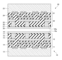
- step S3 the surface 10a of the first substrate 10 and the surface 20a of the second substrate 20 are bonded via the liquid films 18, 28.
- the surface 10a of the first substrate 10 and the surface 20a of the second substrate 20 are held facing each other, and the first substrate 10 and the second substrate 20 are aligned.
- the alignment includes, for example, making the electrode pads 15 and 25 face each other.
- the alignment includes, for example, making the second insulating film 17 and the second insulating film 27 face each other.
- the surface 10a of the first substrate 10 and the surface 20a of the second substrate 20 are heated.
- the first substrate 10 and the second substrate 20 are pressed together by bringing them closer together.
- the surface 10a of the first substrate 10 and the surface 20a of the second substrate 20 are brought into close contact.
- the ionic liquid obtained by liquefying the liquid films 18 and 28 dissolves the electrode pads 15 and 25. Therefore, metal-metal bonds and metal-carbon-metal bonds are generated through the ionic liquid, and the contact resistance between the electrode pads 15 and 25 is reduced.
- the ionic liquid present on the bonding surface of the first substrate 10 and the second substrate 20 is pushed out and removed. Therefore, it is not necessary to remove the liquid films 18 and 28 before joining the surface 10a of the first substrate 10 and the surface 20a of the second substrate 20.
- the electrode pad 15 and the electrode pad 25 are formed of the same material, galvanic corrosion does not occur even if the electrode pad 15 and the electrode pad 25 come into contact with each other via the ionic liquid.
- THTDP-DcO is used as the ionic liquid, it is preferable to heat the first substrate 10 and the second substrate 20 to 230° C. to 240° C. in step S3.
- step S3 for example, the first substrate 10 and the second substrate 20 may be pressed together, and then the first substrate 10 and the second substrate 20 may be heated to a temperature at which the liquid films 18 and 28 are liquefied.
- step S3 the surface 10a of the first substrate 10 and the surface 20a of the second substrate 20 may be joined via the liquid films 18 and 28 in a vacuum atmosphere.
- the surfaces of the electrode pads 15 and 25 do not come into contact with oxidizing gas or moisture, oxidative corrosion can be suppressed.
- the ionic liquid is difficult to volatilize even in a vacuum atmosphere and a high temperature environment, the liquid films 18 and 28 do not disappear before the surface 10a of the first substrate 10 and the surface 20a of the second substrate 20 are bonded.
- an ionic liquid is applied to the bonding surface of at least one of the first substrate 10 and the second substrate 20, and then the ionic liquid is applied to the bonding surface of the first substrate 10.
- the surface 10a and the surface 20a of the second substrate 20 are bonded.
- the first substrate 10 and the second substrate 20 can be bonded together while the bonding surfaces of the first substrate 10 and the second substrate 20 are protected by the ionic liquid. Therefore, oxidation of the bonding surface between the first substrate 10 and the second substrate 20 can be suppressed.
- the bonding method according to the embodiment when bonding the surface 10a of the first substrate 10 and the surface 20a of the second substrate 20, the ionic liquid on the bonding surface of the first substrate 10 and the second substrate 20 is extruded. removed. Therefore, it is not necessary to remove the ionic liquid films 18 and 28 before bonding the surface 10a of the first substrate 10 and the surface 20a of the second substrate 20.
- the surface 10a of the first substrate 10 and the surface 20a of the second substrate 20 are bonded via the liquid films 18 and 28 in a vacuum atmosphere. Therefore, the surfaces of the electrode pads 15, 25 do not come into contact with oxidizing gas or moisture, so oxidative corrosion can be suppressed. Since the ionic liquid is difficult to volatilize even in a vacuum atmosphere and a high temperature environment, the liquid films 18 and 28 do not disappear before the surface 10a of the first substrate 10 and the surface 20a of the second substrate 20 are bonded. Therefore, when the first substrate 10 and the second substrate 20 are pressure-bonded, degassing is less likely to occur from the liquid films 18 and 28. Furthermore, since the crimped surfaces can be kept in a vacuum state in a high-temperature environment, very strong adhesion can be obtained.
- the ionic liquid melts the electrode pads 15 and 25 when bonding the surface 10a of the first substrate 10 and the surface 20a of the second substrate 20. Therefore, metal-metal bonds and metal-carbon-metal bonds are generated through the ionic liquid, and the contact resistance between the electrode pads 15 and 25 is reduced.
- Another example of conventional hybrid bonding is a method in which a conductive adhesive is applied to the bonding surface after the bonding surface of the substrate is flattened by CMP, and conductive films are bonded to each other via the conductive adhesive.
- resistance tends to increase due to the conductive adhesive.
- leakage current tends to flow between adjacent conductive films via the conductive adhesive.
- the substrates are bonded to each other via the ionic liquid, so the conductive films are bonded to each other with strong adhesion. Therefore, it is possible to suppress the generation of voids at the bonding surfaces between the conductive films. Moreover, according to the bonding method according to the embodiment, when bonding the substrates together, unnecessary ionic liquid is pushed out from the bonding surface, and ionic liquid between adjacent conductive films is removed. Therefore, leakage current is less likely to flow between adjacent conductive films.
- the bonding apparatus has a processing container 100 whose interior can be sealed.
- a loading/unloading port 101 for transporting the upper substrate WU, lower substrate WL, and overlapping substrate WT is provided on the side surface of the processing container 100 on the positive side in the X direction.
- the loading/unloading exit 101 is opened and closed by an opening/closing shutter 102 .
- the inside of the processing container 100 is divided by an inner wall 103 into a transport area T1 and a processing area T2.
- the carry-in/out port 101 is formed on the side surface of the processing container 100 in the transfer region T1.
- the inner wall 103 is formed with a loading/unloading port 104 for transporting the upper substrate WU, the lower substrate WL, and the superposed substrate WT.
- the loading/unloading port 104 is opened and closed by a gate valve 105 . Gate valve 105 may not be provided.
- a transition 110 for temporarily placing the upper substrate WU, lower substrate WL, and overlapping substrate WT is provided on the positive side of the transport area T1 in the X direction.
- the transition 110 is formed, for example, in two stages, and any two of the upper substrate WU, the lower substrate WL, and the overlapping substrate WT can be placed thereon at the same time.
- a substrate transport body 112 that is movable on a transport path 111 extending in the X direction is provided in the transport region T1.
- the substrate transport body 112 is movable in the vertical direction and around the vertical axis, and transports the upper substrate WU, the lower substrate WL, and the overlapping substrate WT within the transport region T1 or between the transport region T1 and the processing region T2. .
- a position adjustment mechanism 120 that adjusts the horizontal orientations of the upper substrate WU and the lower substrate WL is provided on the negative side of the transport area T1 in the X direction.
- a rail 130 extending along the Y direction is provided on the negative side of the position adjustment mechanism 120 in the X direction in the transport region T1.
- the rail 130 is provided, for example, from the outside of the position adjustment mechanism 120 on the negative side in the Y direction to the outside on the positive side in the Y direction.
- two nozzle arms 131 and 132 are attached to the rail 130.
- the nozzle arm 131 supports a nozzle 133 that discharges an ionic liquid.
- the nozzle arm 131 is movable on the rail 130 by a nozzle drive section 134. Thereby, the nozzle 133 can move from the positive side of the position adjustment mechanism 120 in the Y direction to above the upper substrate WU and lower substrate WL held by the position adjustment mechanism 120.
- the nozzle arm 131 can be moved up and down by the nozzle drive unit 134, and the height of the nozzle 133 can be adjusted.
- a supply pipe (not shown) that supplies the ionic liquid to the nozzle 133 is connected to the nozzle 133 .
- the supply pipe is provided with a heating mechanism such as a heater that heats the ionic liquid flowing inside.
- the nozzle arm 132 supports a nozzle 150 that discharges the ionic liquid.
- the nozzle arm 132 is movable on the rail 130 by the nozzle drive section 151. Thereby, the nozzle 150 can move from the negative side of the position adjustment mechanism 120 in the Y direction to above the upper substrate WU and the lower substrate WL held by the position adjustment mechanism 120.
- the nozzle arm 132 can be moved up and down by the nozzle drive section 151, and the height of the nozzle 150 can be adjusted.
- a supply pipe (not shown) that supplies the ionic liquid to the nozzle 150 is connected to the nozzle 150 .
- the supply pipe is provided with a heating mechanism such as a heater that heats the ionic liquid flowing inside. Only one of the nozzle 133 and the nozzle 150 may be provided.
- the processing area T2 is provided with a lower chuck 160 that places and holds the lower substrate WL on its upper surface, and an upper chuck 161 that suctions and holds the upper substrate WU on its lower surface.
- the lower chuck 160 and the upper chuck 161 are accommodated in the processing area T2.
- the upper chuck 161 is provided above the lower chuck 160.
- the upper chuck 161 is configured to be disposed opposite to the lower chuck 160. That is, the lower substrate WL held by the lower chuck 160 and the upper substrate WU held by the upper chuck 161 can be placed facing each other.
- an electrostatic adsorption electrode (not shown) electrically connected to a DC power source (not shown) or a suction pipe (not shown) connected to a vacuum pump (not shown). ) will be provided inside the lower chuck 160.
- the lower substrate WL is attracted and held on the upper surface of the lower chuck 160 by an electrostatic force such as a Coulomb force generated in an electrode for electrostatic attraction or by suction from a suction tube.
- a heating mechanism 160a such as a heater is provided inside the lower chuck 160.
- the heating mechanism 160a heats the lower substrate WL held by the lower chuck 160 by suction.
- a chuck driving section 163 is provided below the lower chuck 160 via a shaft 162.
- the chuck driver 163 is configured to move the lower chuck 160 up and down.
- the chuck driver 163 may be configured to move the lower chuck 160 in the horizontal direction.
- the chuck driver 163 may be configured to rotate the lower chuck 160 around a vertical axis.
- an electrostatic adsorption electrode (not shown) electrically connected to a DC power source (not shown) or a suction pipe (not shown) connected to a vacuum pump (not shown). ) will be provided inside the upper chuck 161 inside the upper chuck 161.
- the upper substrate WU is attracted and held on the lower surface of the upper chuck 161 by an electrostatic force such as a Coulomb force generated in an electrode for electrostatic attraction or by suction from a suction tube.
- a heating mechanism 161a such as a heater is provided inside the upper chuck 161.
- the heating mechanism 161a heats the upper substrate WU held by the upper chuck 161 by suction.
- a rail 164 extending along the Y direction is provided above the upper chuck 161.
- the upper chuck 161 is movable on the rail 164 by a chuck drive unit 165.
- the chuck driver 165 is configured to move the upper chuck 161 up and down.
- the chuck driver 165 may be configured to rotate the upper chuck 161 around a vertical axis.
- a reversing mechanism 170 that moves between the transport area T1 and the processing area T2 and reverses the front and back surfaces of the upper substrate WU is provided in the transport area T1.
- the reversing mechanism 170 has a holding arm 171 that holds the upper substrate WU.
- a suction pad (not shown) is provided on the holding arm 171 to suction the upper substrate WU and hold it horizontally.
- Holding arm 171 is supported by drive section 173.
- the drive unit 173 is configured to rotate the holding arm 171 around a horizontal axis, and is configured to extend and contract the holding arm 171 in the horizontal direction.
- a drive unit 174 is provided below the drive unit 173 .
- the drive unit 174 is configured to rotate the drive unit 173 around a vertical axis, and is configured to move the drive unit 173 up and down in the vertical direction.
- the drive unit 174 is attached to a rail 175 extending in the Y direction.
- the rails 175 extend from the processing area T2 to the transport area T1.
- the reversing mechanism 170 is movable between the position adjustment mechanism 120 and the upper chuck 161 along a rail 175 by a drive section 174.
- the configuration of the reversing mechanism 170 is not limited to this, as long as it can reverse the front and back surfaces of the upper substrate WU.
- the reversing mechanism 170 may be provided in the processing area T2, for example. Further, a reversing mechanism may be provided on the substrate transport body 112, and another transport mechanism may be provided at the position of the reversing mechanism 170.
- An exhaust port 181 is provided on the side surface of the processing container 100 in the processing region T2.
- An exhaust passage 182 is connected to the exhaust port 181.
- a pressure regulating valve 183 and a vacuum pump 184 are sequentially provided in the exhaust passage 182 so that the processing region T2 can be evacuated.
- the operation of the bonding apparatus when bonding the upper substrate WU and the lower substrate WL will be described.
- the lower substrate WL corresponds to the first substrate 10 and the upper substrate WU corresponds to the second substrate 20.
- the upper substrate WU is transported to the bonding device.
- the upper substrate WU is transported to the position adjustment mechanism 120 by the substrate transport body 112 via the transition 110.
- the nozzle 133 is moved above the center of the upper substrate WU by the nozzle arm 131.
- the ionic liquid is supplied from the nozzle 133 to the surface of the upper substrate WU while rotating the upper substrate WU.
- the supplied ionic liquid is diffused onto the surface of the upper substrate WU by centrifugal force, and the ionic liquid is applied to the surface (step S2 in FIG. 1).
- the horizontal orientation of the upper substrate WU is adjusted by the position adjustment mechanism 120.
- the upper substrate WU is transferred from the position adjustment mechanism 120 to the holding arm 171 of the reversing mechanism 170.
- the holding arm 171 is reversed, so that the front and back surfaces of the upper substrate WU are reversed. That is, the surface of the upper substrate WU is directed downward.
- the reversing mechanism 170 moves toward the upper chuck 161, and the upper substrate WU is transferred from the reversing mechanism 170 to the upper chuck 161.
- the back surface of the upper substrate WU is held by the upper chuck 161 by suction.
- the upper chuck 161 is moved by the chuck driver 165 to a position above the lower chuck 160 and facing the lower chuck 160 .
- the upper substrate WU waits on the upper chuck 161 until a lower substrate WL, which will be described later, is transported to a bonding apparatus. Note that the front and back surfaces of the upper substrate WU may be reversed while the reversing mechanism 170 is moving.
- the lower substrate WL is carried into the bonding apparatus.
- the lower substrate WL is transported to the position adjustment mechanism 120 by the substrate transport body 112 via the transition 110.
- the nozzle 133 is moved by the nozzle arm 131 above the center of the lower substrate WL.
- the ionic liquid is supplied from the nozzle 133 to the surface of the lower substrate WL.
- the supplied ionic liquid is diffused onto the surface of the lower substrate WL by centrifugal force, and the ionic liquid is applied to the surface (step S2 in FIG. 1).
- the horizontal orientation of the lower substrate WL is adjusted by the position adjustment mechanism 120.
- the lower substrate WL is transported to the lower chuck 160 by the substrate transport body 112, and is held by the lower chuck 160 by suction. At this time, the back surface of the lower substrate WL is held by the lower chuck 160 so that the front surface of the lower substrate WL faces upward. Note that a groove (not shown) that matches the shape of the substrate carrier 112 is formed on the upper surface of the lower chuck 160 to prevent interference between the substrate carrier 112 and the lower chuck 160 when transferring the lower substrate WL. You may try to avoid it.
- the gate valve 105 closes the loading/unloading port 104, and the vacuum pump 184 evacuates the processing region T2 to reduce the pressure.
- the horizontal positions of the lower substrate WL held by the lower chuck 160 and the upper substrate WU held by the upper chuck 161 are adjusted. Specifically, first, images of the surface of the lower substrate WL and the surface of the upper substrate WU are taken using, for example, a CCD camera. Based on the captured image, the upper chuck is adjusted so that a predetermined reference point (not shown) on the surface of the lower substrate WL matches a reference point (not shown) on the surface of the upper substrate WU. 161, the horizontal position of the upper substrate WU is adjusted. Note that when the lower chuck 160 is horizontally movable by the chuck driving unit 163, the lower chuck 160 may adjust the horizontal position of the lower substrate WL. Further, the relative horizontal positions of the lower substrate WL and the upper substrate WU may be adjusted using both the lower chuck 160 and the upper chuck 161.
- the lower chuck 160 is raised by the chuck drive unit 163, and the surface of the lower substrate WL held by the lower chuck 160 and the surface of the upper substrate WU held by the upper chuck 161 are brought into contact and pressed together. Further, the heating mechanism 160a heats the lower substrate WL, and the heating mechanism 161a heats the upper substrate WU. As a result, the upper substrate WU and the lower substrate WL are bonded together via the ionic liquid, and the overlapping substrate WT is formed (step S3 in FIG. 1).
- Second substrate 10 First substrate 10a Surface 15 Electrode pad 17 Second insulating film 18 Liquid film 20 Second substrate 20a Surface 25 Electrode pad 27 Second insulating film 28 Liquid film A11, A21 First region A12, A22 Second region
Landscapes
- Engineering & Computer Science (AREA)
- Mechanical Engineering (AREA)
- Chemical & Material Sciences (AREA)
- Chemical Kinetics & Catalysis (AREA)
- General Chemical & Material Sciences (AREA)
- Wire Bonding (AREA)
- Internal Circuitry In Semiconductor Integrated Circuit Devices (AREA)
- Manufacturing & Machinery (AREA)
- Pressure Welding/Diffusion-Bonding (AREA)
Abstract
Description
近年、VLSI(Very Large-Scale Integration)の微細化、立体形化と共に、別々に作製された異なる基板の上に形成した電子回路素子同士を直接貼り合わせて1つの電子回路素子として造り込む3次元積層技術が注目されている。特に、一方の基板の絶縁膜及び導電膜を、それぞれ他方の基板の絶縁膜及び導電膜に同時に貼り合わせて圧着するハイブリッド接合は、VLSIの更なる高速化と低消費電力化のために重要である。導電膜は、例えば電極パッドであり、電気信号の入出力のために用いられる。
図1~図7を参照し、実施形態に係る接合方法について説明する。図1に示されるように、実施形態に係る接合方法はステップS1~S3を有する。ステップS1~S3は、この順に実施される。
図8及び図9を参照し、実施形態に係る接合方法を実施するための接合装置について説明する。
接合装置において、上基板WUと下基板WLとを接合する場合の動作について説明する。下基板WLは第1基板10に対応し、上基板WUは第2基板20に対応する。
10a 表面
15 電極パッド
17 第2絶縁膜
18 液膜
20 第2基板
20a 表面
25 電極パッド
27 第2絶縁膜
28 液膜
A11,A21 第1領域
A12,A22 第2領域
Claims (13)
- 絶縁膜が露出する第1領域と、導電膜が露出する第2領域とを表面に有する第1基板及び第2基板を準備する工程と、
前記第1基板及び前記第2基板の少なくとも一方の前記表面にイオン液体を塗布する工程と、
前記イオン液体を介して前記第1基板の前記表面と前記第2基板の前記表面とを接合する工程と、
を有する、接合方法。 - 前記準備する工程は、化学的機械研磨により前記第1基板の表面及び前記第2基板の表面を処理する工程を含む、
請求項1に記載の接合方法。 - 前記塗布する工程は、前記第1基板の表面及び前記第2基板の表面に前記イオン液体を塗布する工程を含む、
請求項1に記載の接合方法。 - 前記接合する工程は、
前記第1基板と前記第2基板とを圧着する工程と、
前記第1基板及び前記第2基板を加熱する工程と、
を含む、
請求項1に記載の接合方法。 - 前記塗布する工程は、前記第1基板及び前記第2基板の少なくとも一方の前記表面に塗布された前記イオン液体をゲル化させることを含み、
前記加熱する工程は、前記塗布する工程においてゲル化した前記イオン液体を液化させることを含む、
請求項4に記載の接合方法。 - 前記接合する工程は、真空雰囲気下で行われる、
請求項1に記載の接合方法。 - 前記第1基板の表面に露出する導電膜と、前記第2基板の表面に露出する導電膜とは、同じ材料により形成される、
請求項1に記載の接合方法。 - 前記イオン液体は、THTDP-DcOである、
請求項1に記載の接合方法。 - 絶縁膜が露出する第1領域と、導電膜が露出する第2領域とを表面に有する第1基板及び第2基板の少なくとも一方の前記表面にイオン液体を塗布する塗布機構と、
前記第1基板の表面と前記第2基板の表面とを対向させてそれぞれ保持する第1保持部及び第2保持部と、
前記第1保持部及び前記第2保持部を相対的に接近させることにより、前記第1基板の前記表面と前記第2基板の前記表面とを密着させる駆動機構と、
を備える、
接合装置。 - 前記第1保持部及び前記第2保持部にそれぞれ保持された前記第1基板及び前記第2基板を加熱する加熱機構を更に備える、
請求項9に記載の接合装置。 - 前記第1保持部及び前記第2保持部を収容する処理容器と、
前記処理容器の内部を排気する真空ポンプと、
を更に備える、
請求項9に記載の接合装置。 - 前記第1基板の表面に露出する導電膜と、前記第2基板の表面に露出する導電膜とは、同じ材料により形成される、
請求項9に記載の接合装置。 - 前記イオン液体は、THTDP-DcOである、
請求項9に記載の接合装置。
Priority Applications (2)
| Application Number | Priority Date | Filing Date | Title |
|---|---|---|---|
| KR1020257003295A KR20250029228A (ko) | 2022-07-13 | 2023-07-03 | 접합 방법 및 접합 장치 |
| US19/010,575 US20250144892A1 (en) | 2022-07-13 | 2025-01-06 | Bonding method and bonding apparatus |
Applications Claiming Priority (2)
| Application Number | Priority Date | Filing Date | Title |
|---|---|---|---|
| JP2022112651A JP7845794B2 (ja) | 2022-07-13 | 2022-07-13 | 接合方法及び接合装置 |
| JP2022-112651 | 2022-07-13 |
Related Child Applications (1)
| Application Number | Title | Priority Date | Filing Date |
|---|---|---|---|
| US19/010,575 Continuation US20250144892A1 (en) | 2022-07-13 | 2025-01-06 | Bonding method and bonding apparatus |
Publications (1)
| Publication Number | Publication Date |
|---|---|
| WO2024014342A1 true WO2024014342A1 (ja) | 2024-01-18 |
Family
ID=89536614
Family Applications (1)
| Application Number | Title | Priority Date | Filing Date |
|---|---|---|---|
| PCT/JP2023/024636 Ceased WO2024014342A1 (ja) | 2022-07-13 | 2023-07-03 | 接合方法及び接合装置 |
Country Status (4)
| Country | Link |
|---|---|
| US (1) | US20250144892A1 (ja) |
| JP (1) | JP7845794B2 (ja) |
| KR (1) | KR20250029228A (ja) |
| WO (1) | WO2024014342A1 (ja) |
Citations (6)
| Publication number | Priority date | Publication date | Assignee | Title |
|---|---|---|---|---|
| JP2013251405A (ja) * | 2012-05-31 | 2013-12-12 | Tadatomo Suga | 金属領域を有する基板の接合方法 |
| WO2014157227A1 (ja) * | 2013-03-26 | 2014-10-02 | 富士フイルム株式会社 | 半導体装置製造用仮接合用積層体、および、半導体装置の製造方法 |
| JP2021157934A (ja) * | 2020-03-26 | 2021-10-07 | 株式会社ジャパンディスプレイ | 表示装置及び表示装置 |
| WO2021220883A1 (ja) * | 2020-04-28 | 2021-11-04 | 東京エレクトロン株式会社 | 半導体装置の製造方法、半導体製造装置及びシステム |
| JP2023105682A (ja) * | 2022-01-19 | 2023-07-31 | 東京エレクトロン株式会社 | 基板処理方法及び基板処理システム |
| JP2023105681A (ja) * | 2022-01-19 | 2023-07-31 | 東京エレクトロン株式会社 | 基板処理方法及びイオン液体 |
Family Cites Families (4)
| Publication number | Priority date | Publication date | Assignee | Title |
|---|---|---|---|---|
| JP4727556B2 (ja) | 2006-11-28 | 2011-07-20 | 株式会社フジクラ | 実装基板およびその製造方法 |
| JP2017098463A (ja) | 2015-11-26 | 2017-06-01 | 日立化成株式会社 | 半導体用接着剤、半導体装置の製造方法及び半導体装置 |
| US12406959B2 (en) | 2018-07-26 | 2025-09-02 | Adeia Semiconductor Bonding Technologies Inc. | Post CMP processing for hybrid bonding |
| JP2020050850A (ja) | 2018-09-28 | 2020-04-02 | 日東電工株式会社 | 被着体の接合・分離方法 |
-
2022
- 2022-07-13 JP JP2022112651A patent/JP7845794B2/ja active Active
-
2023
- 2023-07-03 KR KR1020257003295A patent/KR20250029228A/ko active Pending
- 2023-07-03 WO PCT/JP2023/024636 patent/WO2024014342A1/ja not_active Ceased
-
2025
- 2025-01-06 US US19/010,575 patent/US20250144892A1/en active Pending
Patent Citations (6)
| Publication number | Priority date | Publication date | Assignee | Title |
|---|---|---|---|---|
| JP2013251405A (ja) * | 2012-05-31 | 2013-12-12 | Tadatomo Suga | 金属領域を有する基板の接合方法 |
| WO2014157227A1 (ja) * | 2013-03-26 | 2014-10-02 | 富士フイルム株式会社 | 半導体装置製造用仮接合用積層体、および、半導体装置の製造方法 |
| JP2021157934A (ja) * | 2020-03-26 | 2021-10-07 | 株式会社ジャパンディスプレイ | 表示装置及び表示装置 |
| WO2021220883A1 (ja) * | 2020-04-28 | 2021-11-04 | 東京エレクトロン株式会社 | 半導体装置の製造方法、半導体製造装置及びシステム |
| JP2023105682A (ja) * | 2022-01-19 | 2023-07-31 | 東京エレクトロン株式会社 | 基板処理方法及び基板処理システム |
| JP2023105681A (ja) * | 2022-01-19 | 2023-07-31 | 東京エレクトロン株式会社 | 基板処理方法及びイオン液体 |
Also Published As
| Publication number | Publication date |
|---|---|
| KR20250029228A (ko) | 2025-03-04 |
| US20250144892A1 (en) | 2025-05-08 |
| JP2024011003A (ja) | 2024-01-25 |
| JP7845794B2 (ja) | 2026-04-14 |
Similar Documents
| Publication | Publication Date | Title |
|---|---|---|
| US9666573B1 (en) | Methods of forming integrated circuitry | |
| US9331032B2 (en) | Hybrid bonding and apparatus for performing the same | |
| TW570856B (en) | Solder jointing system, solder jointing method, semiconductor device manufacturing method, and semiconductor device manufacturing system | |
| US20170243910A1 (en) | Semiconductor device and method for manufacturing semiconductor device | |
| US9093447B2 (en) | Chip on wafer bonder | |
| CN103212776B (zh) | 电子器件、制造方法和电子器件制造装置 | |
| US20090197390A1 (en) | Lock and key structure for three-dimentional chip connection and process thereof | |
| TW201944500A (zh) | 低溫接合結構 | |
| CN104253086B (zh) | 用于金属氧化物还原的预处理方法和所形成的器件 | |
| JP2009049081A (ja) | 接合装置 | |
| US20240387445A1 (en) | Wafer bonding system and method of using the same | |
| TW202226380A (zh) | 基板接合系統及基板接合方法 | |
| US20250343187A1 (en) | Bonding layer and process of making | |
| CN101667528A (zh) | 用于三维ic互连的衬底对衬底键合装置和方法 | |
| JP7845794B2 (ja) | 接合方法及び接合装置 | |
| JP2005086089A (ja) | 3次元デバイスの製造方法 | |
| CN110546744B (zh) | 绝缘膜的成膜方法、绝缘膜的成膜装置及基板处理系统 | |
| US20250349789A1 (en) | Bonding method and bonding apparatus | |
| TW561549B (en) | Thin film forming apparatus and thin film forming method | |
| US20260116044A1 (en) | Device bonding | |
| US20250300124A1 (en) | Substrate bonding method and substrate bonding apparatus | |
| US20250379184A1 (en) | Self-alignment for bonding of semiconductor devices | |
| US20240194478A1 (en) | Apparatus and methods for processing bonding semiconductor wafers | |
| JP2005072044A (ja) | 配線形成装置 | |
| CN119626917A (zh) | 一种半导体器件及其制造方法 |
Legal Events
| Date | Code | Title | Description |
|---|---|---|---|
| 121 | Ep: the epo has been informed by wipo that ep was designated in this application |
Ref document number: 23839514 Country of ref document: EP Kind code of ref document: A1 |
|
| ENP | Entry into the national phase |
Ref document number: 20257003295 Country of ref document: KR Kind code of ref document: A |
|
| WWE | Wipo information: entry into national phase |
Ref document number: 1020257003295 Country of ref document: KR |
|
| NENP | Non-entry into the national phase |
Ref country code: DE |
|
| WWP | Wipo information: published in national office |
Ref document number: 1020257003295 Country of ref document: KR |
|
| 122 | Ep: pct application non-entry in european phase |
Ref document number: 23839514 Country of ref document: EP Kind code of ref document: A1 |