WO2024010021A1 - 基板、電子装置、電子モジュールおよびモジュール装置 - Google Patents
基板、電子装置、電子モジュールおよびモジュール装置 Download PDFInfo
- Publication number
- WO2024010021A1 WO2024010021A1 PCT/JP2023/024867 JP2023024867W WO2024010021A1 WO 2024010021 A1 WO2024010021 A1 WO 2024010021A1 JP 2023024867 W JP2023024867 W JP 2023024867W WO 2024010021 A1 WO2024010021 A1 WO 2024010021A1
- Authority
- WO
- WIPO (PCT)
- Prior art keywords
- recess
- film layer
- substrate according
- volume
- substrate
- Prior art date
- Legal status (The legal status is an assumption and is not a legal conclusion. Google has not performed a legal analysis and makes no representation as to the accuracy of the status listed.)
- Ceased
Links
Images







Classifications
-
- H—ELECTRICITY
- H01—ELECTRIC ELEMENTS
- H01S—DEVICES USING THE PROCESS OF LIGHT AMPLIFICATION BY STIMULATED EMISSION OF RADIATION [LASER] TO AMPLIFY OR GENERATE LIGHT; DEVICES USING STIMULATED EMISSION OF ELECTROMAGNETIC RADIATION IN WAVE RANGES OTHER THAN OPTICAL
- H01S5/00—Semiconductor lasers
- H01S5/02—Structural details or components not essential to laser action
- H01S5/022—Mountings; Housings
- H01S5/023—Mount members, e.g. sub-mount members
- H01S5/02315—Support members, e.g. bases or carriers
-
- H—ELECTRICITY
- H10—SEMICONDUCTOR DEVICES; ELECTRIC SOLID-STATE DEVICES NOT OTHERWISE PROVIDED FOR
- H10W—GENERIC PACKAGES, INTERCONNECTIONS, CONNECTORS OR OTHER CONSTRUCTIONAL DETAILS OF DEVICES COVERED BY CLASS H10
- H10W40/00—Arrangements for thermal protection or thermal control
- H10W40/20—Arrangements for cooling
- H10W40/25—Arrangements for cooling characterised by their materials
- H10W40/255—Arrangements for cooling characterised by their materials having a laminate or multilayered structure, e.g. direct bond copper [DBC] ceramic substrates
-
- H—ELECTRICITY
- H01—ELECTRIC ELEMENTS
- H01S—DEVICES USING THE PROCESS OF LIGHT AMPLIFICATION BY STIMULATED EMISSION OF RADIATION [LASER] TO AMPLIFY OR GENERATE LIGHT; DEVICES USING STIMULATED EMISSION OF ELECTROMAGNETIC RADIATION IN WAVE RANGES OTHER THAN OPTICAL
- H01S5/00—Semiconductor lasers
- H01S5/02—Structural details or components not essential to laser action
- H01S5/022—Mountings; Housings
- H01S5/0233—Mounting configuration of laser chips
- H01S5/02345—Wire-bonding
-
- H—ELECTRICITY
- H01—ELECTRIC ELEMENTS
- H01S—DEVICES USING THE PROCESS OF LIGHT AMPLIFICATION BY STIMULATED EMISSION OF RADIATION [LASER] TO AMPLIFY OR GENERATE LIGHT; DEVICES USING STIMULATED EMISSION OF ELECTROMAGNETIC RADIATION IN WAVE RANGES OTHER THAN OPTICAL
- H01S5/00—Semiconductor lasers
- H01S5/02—Structural details or components not essential to laser action
- H01S5/024—Arrangements for thermal management
- H01S5/02469—Passive cooling, e.g. where heat is removed by the housing as a whole or by a heat pipe without any active cooling element like a TEC
-
- H—ELECTRICITY
- H01—ELECTRIC ELEMENTS
- H01S—DEVICES USING THE PROCESS OF LIGHT AMPLIFICATION BY STIMULATED EMISSION OF RADIATION [LASER] TO AMPLIFY OR GENERATE LIGHT; DEVICES USING STIMULATED EMISSION OF ELECTROMAGNETIC RADIATION IN WAVE RANGES OTHER THAN OPTICAL
- H01S5/00—Semiconductor lasers
- H01S5/02—Structural details or components not essential to laser action
- H01S5/024—Arrangements for thermal management
- H01S5/02476—Heat spreaders, i.e. improving heat flow between laser chip and heat dissipating elements
-
- H—ELECTRICITY
- H05—ELECTRIC TECHNIQUES NOT OTHERWISE PROVIDED FOR
- H05K—PRINTED CIRCUITS; CASINGS OR CONSTRUCTIONAL DETAILS OF ELECTRIC APPARATUS; MANUFACTURE OF ASSEMBLAGES OF ELECTRICAL COMPONENTS
- H05K1/00—Printed circuits
- H05K1/02—Details
- H05K1/0201—Thermal arrangements, e.g. for cooling, heating or preventing overheating
- H05K1/0203—Cooling of mounted components
- H05K1/0204—Cooling of mounted components using means for thermal conduction connection in the thickness direction of the substrate
-
- H—ELECTRICITY
- H05—ELECTRIC TECHNIQUES NOT OTHERWISE PROVIDED FOR
- H05K—PRINTED CIRCUITS; CASINGS OR CONSTRUCTIONAL DETAILS OF ELECTRIC APPARATUS; MANUFACTURE OF ASSEMBLAGES OF ELECTRICAL COMPONENTS
- H05K2201/00—Indexing scheme relating to printed circuits covered by H05K1/00
- H05K2201/10—Details of components or other objects attached to or integrated in a printed circuit board
- H05K2201/10227—Other objects, e.g. metallic pieces
- H05K2201/10416—Metallic blocks or heatsinks completely inserted in a PCB
-
- H—ELECTRICITY
- H10—SEMICONDUCTOR DEVICES; ELECTRIC SOLID-STATE DEVICES NOT OTHERWISE PROVIDED FOR
- H10W—GENERIC PACKAGES, INTERCONNECTIONS, CONNECTORS OR OTHER CONSTRUCTIONAL DETAILS OF DEVICES COVERED BY CLASS H10
- H10W40/00—Arrangements for thermal protection or thermal control
- H10W40/20—Arrangements for cooling
- H10W40/22—Arrangements for cooling characterised by their shape, e.g. having conical or cylindrical projections
- H10W40/226—Arrangements for cooling characterised by their shape, e.g. having conical or cylindrical projections characterised by projecting parts, e.g. fins to increase surface area
- H10W40/228—Arrangements for cooling characterised by their shape, e.g. having conical or cylindrical projections characterised by projecting parts, e.g. fins to increase surface area the projecting parts being wire-shaped or pin-shaped
-
- H—ELECTRICITY
- H10—SEMICONDUCTOR DEVICES; ELECTRIC SOLID-STATE DEVICES NOT OTHERWISE PROVIDED FOR
- H10W—GENERIC PACKAGES, INTERCONNECTIONS, CONNECTORS OR OTHER CONSTRUCTIONAL DETAILS OF DEVICES COVERED BY CLASS H10
- H10W40/00—Arrangements for thermal protection or thermal control
- H10W40/70—Fillings or auxiliary members in containers or in encapsulations for thermal protection or control
- H10W40/77—Auxiliary members characterised by their shape
- H10W40/778—Auxiliary members characterised by their shape in encapsulations
Definitions
- the present disclosure relates to a board on which components such as electronic elements are mounted.
- Patent Document 1 and Patent Document 2 there are known substrates on which electronic devices are mounted, which have improved thermal conductivity in order to quickly dissipate heat generated from the electronic devices. ing.
- a substrate includes a base including a first surface and a second surface located on the opposite side of the first surface, and the base includes at least one of the first surface and the second surface. At least one recess is provided on one surface, the inside of the recess is filled with a metal member having a thermal conductivity higher than that of the base, and the first surface and In at least one cross section cut in a first direction perpendicular to the second surface, the width of the recess in the direction parallel to the first surface is the width of the recess in the direction parallel to the first surface and the second surface. The value decreases as the distance from the surface increases.
- FIG. 1 is a perspective view of a module device according to Embodiment 1 of the present disclosure.
- FIG. 3 is a top view of the module device.
- FIG. 3 is a sectional view taken along line III-III in FIG. 2;
- FIG. 2 is a top view of a substrate according to Embodiment 1 of the present disclosure.
- 5 is a sectional view taken along line VV in FIG. 4.
- FIG. FIG. 3 is a top view of a substrate according to Embodiment 2 of the present disclosure.
- 7 is a sectional view taken along the line VII-VII in FIG. 6.
- FIG. FIG. 7 is a top view of a substrate according to Embodiment 3 of the present disclosure.
- 9 is a sectional view taken along line IX-IX in FIG. 8;
- FIG. 8 is a sectional view taken along line IX-IX in FIG. 8;
- FIG. 9 is a sectional view taken along the line XX in FIG. 8.
- FIG. FIG. 7 is a top view of a substrate according to Embodiment 4 of the present disclosure.
- FIG. 7 is a diagram of a substrate and an electronic device according to Embodiment 4 of the present disclosure, viewed from the Y-axis direction.
- FIG. 7 is a top view of a substrate according to Embodiment 5 of the present disclosure.
- FIG. 7 is a diagram of a substrate and an electronic device according to Embodiment 5 of the present disclosure, viewed from the Y-axis direction.
- thermal conductivity can be improved.
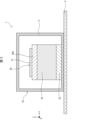
- FIG. 1 is a perspective view of a module device 1 in this embodiment.
- FIG. 2 is a top view of the module device 1.
- FIG. 3 is a sectional view taken along the line III--III in FIG. 2.
- the X-axis direction in FIG. This will be explained as a direction (vertical direction).
- the +X-axis direction is rightward, the -X-axis direction is leftward, the +Y-axis direction is backward, the -Y-axis direction is forward, the +Z-axis direction is upward, and the -Z-axis direction is downward. It will be explained as follows.
- the module device 1 includes an electronic module 10 and a housing 2 in which the electronic module 10 is mounted.
- the housing 2 may be composed of, for example, a cooling plate. Thereby, the electronic module 10 can be cooled.
- the number of electronic modules included in the module device 1 may be one, or two or more.
- the electronic module 10 may be mounted on a module board (not shown) instead of the housing 2.
- the electronic module 10 includes a case 11, a fixing member 12, and an electronic device 20.
- the case 11 has a housing space 11a at the center in the second direction (left-right direction), and the electronic device 20 is housed inside the housing space 11a.
- the case 11 is fixed to the housing 2 by a fixing member 12.
- the fixing member 12 may be, for example, a screw.
- the material of the case 11 may be metal.
- the electronic device 20 includes an electronic element 21, a substrate 30A, a metal plate 22, and a heat sink 23 in this order from above.
- the electronic device 21 in this embodiment is configured by a laser diode or the like that can emit laser, and the electronic device 20 irradiates the laser emitted from the electronic device 21 to the outside.
- the substrate 30A is required to have high heat dissipation properties. Further, a part of the heat conducted to the heat sink 23 is conducted to the casing 2 made of a cooling plate via the case 11, and is radiated in the casing 2.
- the substrate 30A may be an electronic element mounting substrate on which the electronic element 21 is mounted.
- the substrate 30A may be used to mount heat-generating components other than electronic elements.
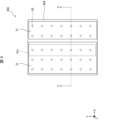
- FIG. 4 is a top view of the substrate 30A.
- an electronic element mounting portion 41a and a recess 50 which will be described later, are shown by dotted lines.
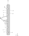
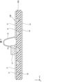
- FIG. 5 is a sectional view taken along line VV in FIG. 4.
- an electronic element 21 is also illustrated.
- the recess 50 is indicated by a dotted line.
- the substrate 30A includes a base body 40A, a first conductive film layer 31, a second conductive film layer 32, and a metal member 51.
- the base 40A may consist of a single layer or multiple layers.
- the base 40A in this embodiment is a single insulating layer as shown in FIG.
- the base 40A has a first surface 41 on which the electronic element 21 is mounted, and a second surface 42 located on the opposite side of the first surface.
- the first surface 41 and the second surface 42 are opposed to each other.
- the first surface 41 includes an electronic element mounting portion 41a in which the electronic element 21 is mounted at the center in the second direction (left-right direction).
- the shape of the base 40A when viewed from above is not particularly limited, and may be, for example, rectangular or circular.
- the base body 40A in this embodiment has a rectangular shape when viewed from above.
- the base 40A may have insulating properties.
- the material of the base 40A is, for example, a ceramic such as an aluminum nitride sintered body, an aluminum oxide sintered body (alumina ceramics), a silicon nitride sintered body, a mullite sintered body, or a glass ceramic sintered body. It may be.
- the material of the base 40A is an aluminum nitride sintered body
- the base 40A contains aluminum nitride as a main component.
- the base 40A when the mass of the base 40A is 100% by mass, the base 40A contains 80% by mass or more of aluminum nitride.
- the base body 40A may contain 95% by mass or more of aluminum nitride. Thereby, the thermal conductivity of the base 40A can be easily set to 170 W/mK or more, so that the heat dissipation performance of the base 40A can be increased.
- the base 40A has at least one recess 50 on the first surface 41.
- the base body 40A has a plurality of recesses 50 on the first surface 41.
- the recess 50 may have a cavity structure.
- the opening of the recess 50 may have a circular shape when the substrate 30A is viewed in plan from the Z-axis direction.
- the recess 50 has a bottom.
- the method of arranging the plurality of recesses 50 is not particularly limited, but for example, as shown in FIG. It may be arranged so that it is located in . In other words, the plurality of recesses 50 may be arranged in a grid-like position. As a result, when the substrate 30A is viewed in plan, the plurality of recesses 50 are evenly arranged, so that variations in heat dissipation of the substrate 30A are less likely to occur.
- the recess 50 is at a distance from the first surface 41 in a cross section taken along a plane parallel to the first direction (that is, the vertical direction) orthogonal to the first surface 41 and the second surface 42. becomes thinner as it gets bigger.
- the width of the recess 50 in the second direction decreases as the distance from the first surface 41 on which the recess 50 is provided increases.
- the shape of the recess 50 may be a curved shape that is convex from the first surface 41 toward the second surface 42 in a cross section taken in the first direction.
- the cross section of the recess 50 taken along a plane parallel to the first direction may have an elliptical hemispherical shape.
- flat or plane does not require that it be strictly flat or strictly flat.
- the recess 50 can be formed by blasting the first surface 41. By forming the recess 50 by blasting, the inner surface of the recess 50 can be formed into a curved shape, as shown in FIG.
- the opening areas of the plurality of recesses 50 are the same when the base body 40A is viewed from above, but the opening area of the plurality of recesses 50 is not limited to this. Good too.
- An example in which the opening areas of the plurality of recesses 50 are not the same will be described in Embodiment 2.
- the depths of the plurality of recesses 50 are the same, but the depth is not limited to this, and the depths of the plurality of recesses 50 may be different from each other.
- the inside of the recess 50 is filled with a metal member 51 having a higher thermal conductivity than that of the base 40A.
- the metal member 51 is not particularly limited as long as it has a thermal conductivity higher than that of the base 40A.
- the material of the base 40A is an aluminum nitride sintered body, it may be made of copper, copper-tungsten, It may be copper-molybdenum, aluminum, etc.
- a plating method such as an electrolytic plating method or a metallization method can be used.
- the substrate 30A may have a thin film layer (not shown) on the surface of the recess 50 and the surface of the first surface 41.
- the thin film layer may be comprised of, for example, tantalum nitride, nickel-chromium, nickel-chromium-silicon, tungsten-silicon, molybdenum-silicon, tungsten, molybdenum, titanium, chromium, and the like.
- the thin film layer can be formed by a formation technique such as a vapor deposition method, an ion plating method, or a sputtering method.
- the thin film layer on the surface of the recess 50 filling of the recess 50 with the metal member 51 and forming the first conductive film layer 31 on the first surface 41 can be performed satisfactorily. It is possible to improve the bonding between the inner surface and the metal member 51, the bond between the first surface 41 and the first conductive film layer 31, and the bond between the metal member 51 and the first conductive film layer 31.
- the coefficient of thermal expansion of the base body 40A and the coefficient of thermal expansion of the metal member 51 become larger. Due to this difference, the base body 40A is warped. When the base body 40A is warped, the contact area between the metal plate 22 and the base body 40A becomes smaller. As a result, heat transfer from the base 40A to the metal plate 22 becomes difficult to occur, and the heat dissipation performance of the electronic device 20 decreases.
- the sum of the volumes of the metal members 51 filled in the plurality of recesses 50 is set to be 10% or less of the volume of the base 40A including the recesses 50. Good too. As a result, the amount of warpage of the base body 40A can be reduced, so that the heat dissipation of the electronic device 20 is less likely to deteriorate.
- the sum of the volumes of the metal members 51 represents the volume of the metal members 51 filled in the recess 50.
- the first conductive film layer 31 is located on the first surface 41 of the base 40A, as shown in FIG.
- the first conductor film layer 31 is connected to a metal member 51 filled in the recess 50 .
- the first conductive film layer 31 is connected to each metal member 51 filled in a plurality of recesses 50 formed in the base 40A.
- the first conductive film layer 31 is made of a material with excellent electrical conductivity, such as copper.
- the first conductive film layer 31 is formed on the first surface 41 in two regions.
- the electronic device 21 is mounted on one first conductor film layer 31 .
- the other first conductive film layer 31 is used as a connection part for a connection member 33 such as a bonding wire, and electrically connects the electronic element 21 and a wiring conductor of a wiring board (not shown).
- a connection member 33 such as a bonding wire
- the electronic element 21 is mounted on the first conductive film layer 31
- the electronic element 21 is mounted on the first conductive film layer 31.
- the description will be made assuming that this is synonymous with "mounted on the electronic element mounting portion 41a of the first surface 41.”
- the first conductive film layer 31 is formed on the first surface 41 and has a higher thermal conductivity than that of the base 40A.
- the first conductive film layer 31 is not particularly limited as long as it has a thermal conductivity higher than that of the base 40A.
- the material of the base 40A is an aluminum nitride sintered body, copper, copper, etc. - May be tungsten, copper-molybdenum, aluminum, etc.
- the first conductive film layer 31 can be formed on the first surface 41 by using a plating method such as an electrolytic plating method or a metallization method.
- the first surface 41 may have a thin film layer (not shown) on the surface. If the first conductive film layer 31 and the metal member 51 are made of the same material, for example, if the first conductive film layer 31 and the metal member 51 are made of copper, then the first conductive film layer 31 and the metal member 51 are made of copper. Good heat transfer can be achieved.
- the electrode of the electronic element 21 and the other first conductor film layer 31 are connected via a connecting member 33 such as a bonding wire. It is mounted on the substrate 30A by being electrically connected to the conductor film layer 31.
- a plating layer may be formed on the upper surface of the first conductor film layer 31.
- the plating layer may be made of a metal having excellent corrosion resistance and connectivity with the connecting member 33, such as nickel, copper, gold, or silver.
- the plating layer may be formed, for example, by sequentially depositing a nickel plating layer with a thickness of 0.5 to 5 ⁇ m and a gold plating layer with a thickness of 0.1 to 3 ⁇ m. This reduces the possibility that the first conductive film layer 31 will corrode, and also strengthens the adhesion between the first conductive film layer 31 and the electronic element 21 and the bond between the first conductive film layer 31 and the connection member 33. can.
- the second conductive film layer 32 is located on the second surface 42 of the base 40A.
- the second conductive film layer 32 may have the same material and configuration as the first conductive film layer 31.
- the second conductive film layer 32 is used for bonding to the metal plate 22. If the second conductor film layer 32 and the metal member 51 are made of the same material, for example, if the second conductor film layer 32 and the metal member 51 are made of copper, then the metal member 51 is made of the same material as the metal member 51. Good heat transfer can be achieved.
- the substrate 30A in this embodiment has a second surface on the first surface on which the electronic element 21 is mounted, as the distance from the first surface 41 increases in a cross section cut along a plane parallel to the first direction.
- a recess 50 whose width in the direction is small is formed.
- the surface area of the recess 50 can be made larger than, for example, when the recess 50 has a rectangular parallelepiped shape.
- heat can be easily transferred from the metal member 51 to the base 40A.
- the thermal conductivity of the substrate 30A can be increased.
- a recess 50 whose width in the front-rear direction decreases as the distance from the first surface 41 increases in a cross section cut along a plane parallel to the first direction. may be formed.
- the shape of the recessed portion 50 is a curved shape that is convex from the first surface 41 toward the second surface 42 in a cross section cut in the first direction.
- the metal member 51 filled in the recess 50 is in contact with the first conductive film layer 31, as shown in FIG. Thereby, the heat conducted from the electronic element 21 to the first conductive film layer 31 can be easily conducted to the metal member 51. Therefore, the thermal conductivity of the substrate 30A can be improved.
- the substrate 30A in this embodiment has a laser diode mounted thereon as the electronic element 21, the electronic element mounted on the substrate 30A is not limited to the laser diode.
- the electronic element mounted on the substrate 30A may be a semiconductor element such as an IC chip or an LSI chip, or a piezoelectric element such as a crystal resonator or a piezoelectric resonator.
- FIG. 6 is a top view of the substrate 30B in this embodiment.
- FIG. 7 is a sectional view taken along line VII-VII in FIG. 6. In FIG. 7, an electronic element 21 is also illustrated.
- the substrate 30B includes a base body 40B in place of the base body 40A in the first embodiment.
- the base body 40B has a plurality of recesses 50 filled with metal members 51 formed on the first surface 41.
- the opening diameter of the recess 50 becomes smaller toward the outside from the center in the second direction of the first surface 41 on which the electronic element 21 is mounted.
- the opening area of the recess 50 increases from the outside in the second direction toward the electronic element mounting portion 41a.
- the opening diameter of the recess 50 becomes smaller as it goes outward from the central part in the third direction of the first surface 41 on which the electronic element 21 is mounted.
- the opening area of the recess 50 increases from the outside in the third direction toward the electronic element mounting portion 41a.
- the opening area of the recess 50 provided in the electronic element mounting part 41a or a region close to the electronic element mounting part 41a is smaller than the opening area of the electronic element mounting part 41a. It is larger than the opening area of the recess 50 provided in the area far from the area.
- the thermal conductivity near the electronic element mounting portion 41a is higher than that at the outer edge portion. This makes it easier to efficiently transfer the heat conducted from the electronic element 21 to the metal plate 22, making it easier to lower the temperature of the electronic element 21.
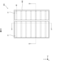
- FIG. 8 is a top view of the substrate 30C in this embodiment.
- FIG. 9 is a sectional view taken along line IX-IX in FIG.
- FIG. 10 is a sectional view taken along line XX in FIG. 8.
- the substrate 30C includes a base body 40C in place of the base body 40A in the first embodiment.
- a plurality of recesses 60 filled with metal members 51 are formed in the first surface 41 of the base 40C.
- the recess 60 is a slit extending in the second direction (horizontal direction), which is a direction perpendicular to the first direction (vertical direction).
- the recess 60 may be provided in a region that overlaps with the first conductor film layer 31 when the base 40C is seen through the plane.
- the recess 60 in this embodiment is formed so that the length in the second direction is the same as the length in the second direction of the first conductive film layer 31; It may be shorter than the length of.
- the term "vertical" does not necessarily mean strictly vertical.
- the length of the recess 60 in the third direction decreases as the distance from the first surface 41 increases.
- the surface area of the recess 60 can be made larger than, for example, when the cross section taken along a plane perpendicular to the second direction has a rectangular shape.
- heat can be easily transferred from the metal member 51 to the base 40C. Thereby, the thermal conductivity of the substrate 30C can be increased.
- the recess 60 in this embodiment is a slit extending in the second direction, it is not limited to this.
- the recess 60 may be a slit extending in any direction as long as it is perpendicular to the first direction; for example, it may be a slit extending in the third direction.
- the slit can be formed by blasting the first surface 41 of the base 40C, as in the above embodiment.
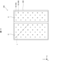
- FIG. 11 is a top view of the substrate 30D in this embodiment.
- the recess 50 formed in the second surface 42 is shown hatched.
- FIG. 12 is a diagram of the substrate 30D and the electronic element 21 viewed from the third direction (front-back direction). In FIG. 12, the recess 50 is indicated by a dotted line.
- the substrate 30D includes a base body 40D in place of the base body 40A in the first embodiment.
- the base body 40D has a plurality of recesses 50 filled with metal members 51 on the first surface 41 and the second surface 42.
- the recess 50 provided on the first surface 41 may be described as a first recess 50A, and the recess 50 provided on the second surface 42 as a second recess 50B.
- the base body 40D may be arranged such that the four adjacent recesses 50 on the first surface 41 and the second surface 42 are located at the apexes of a rectangle.
- the plurality of recesses 50 may be arranged in a grid-like position.
- the plurality of recesses 50 are evenly arranged on the first surface 41 and the second surface 42, so that variations in heat dissipation of the substrate 30D are less likely to occur.
- a metal member 51 filled in a second recess 50B formed on the second surface 42 is connected to the second conductive film layer 32.
- the base body 40D When viewed from above, the base body 40D has a first recess 50A formed in the first surface 41 and a second recess 50B formed in the second surface 42 in at least one direction perpendicular to the first direction. They may be arranged alternately.
- the center of the opening of the first recess 50A formed on the first surface 41 and the opening of the second recess 50B formed on the second surface 42 are aligned on the straight line L shown in FIG. The centers are arranged alternately.
- the base body 40D has at least at least a part of the first recess 50A provided on the first surface overlaps with the second recess 50B provided on the second surface when viewed from a plane perpendicular to the first direction. It may have a set of recesses 50.
- the first recess 50A formed on the first surface 41 is formed deeper than the center of the base 40D in the first direction, and the first recess 50A is formed on the second surface 42. This may be realized by forming the second recess 50B deeper than the center of the base 40D in the first direction. According to this configuration, the volume of the recess 50 formed in the base body 40D can be increased, so that the thermal conductivity of the substrate 30D can be improved.
- the sum of the volume of the metal member 51 filled in the plurality of first recesses 50A provided on the first surface 41 and the volume of the first conductor film layer 31 is the sum of the volume of the plurality of first recesses 50A provided on the first surface 41. If the volume of the metal member 51 filled in the second recess 50B is significantly different from the sum of the volume of the second conductor film layer 32, this is due to the difference between the coefficient of thermal expansion of the base 40D and the coefficient of thermal expansion of the metal member 51. As a result, the base body 40D is warped.
- the sum of the volume of the metal member 51 filled in the plurality of first recesses 50A provided on the first surface 41 and the volume of the first conductive film layer 31 is equal to the volume of the first conductive film layer 31 provided on the second surface 42.
- the sum of the volumes of the metal members 51 filled in the plurality of first recesses 50A provided on the first surface 41 is You may set it so that it may be 90 volume% or more and 110 volume% or less of the sum of the volumes of the metal members 51 filled in the plurality of second recesses 50B provided on the second surface 42.
- the base body 40D has a plurality of recesses 50 filled with the metal member 51 on the first surface 41 and the second surface 42.
- the volume of the metal member 51 included in the base body 40D can be increased compared to the base body 40A in Embodiment 1, so that the thermal conductivity of the substrate 30D can be improved.
- the recesses 50 formed on the first surface 41 and the second surface 42 have a cavity structure, but the structure is not limited to this.
- a plurality of recesses 50 are formed on one of the first surface 41 and the second surface 42, and the slit structure described in Embodiment 3 is formed on the other surface.
- a recess 60 may be formed.
- a recess 60 having a slit structure may be formed on the first surface 41 and the second surface 42.
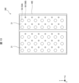
- FIG. 13 is a top view of the substrate 30E in this embodiment.
- the recess 50 formed in the second surface 42 is illustrated with hatching.
- FIG. 14 is a diagram of the substrate 30E and the electronic element 21 viewed from the third direction (front-back direction). In FIG. 14, the recess 50 is indicated by a dotted line.
- the substrate 30E includes a base body 40E in place of the base body 40A in the first embodiment.
- the base body 40E has a plurality of recesses 50 filled with metal members 51 on the first surface 41 and the second surface 42.
- the depth is deeper than the depth of the first recess 50A provided in the first surface 41.
- the sum of the volume of the metal member 51 filled in the plurality of first recesses 50A provided on the first surface 41 and the volume of the first conductive film layer 31 is equal to the volume of the second surface 42. If the volume of the metal member 51 filled in the plurality of second recesses 50B provided in the second recesses 50B is significantly different from the sum of the volume of the second conductor film layer 32, the base body 40E will warp. Therefore, in the base body 40E in this embodiment, as shown in FIG. may also be configured to be smaller. Thereby, the volume of the first recess 50A formed on the first surface 41 and the volume of the second recess 50B formed on the second surface 42 can be prevented from differing greatly. Thereby, the amount of warpage of the base body 40E can be reduced.
- a substrate according to aspect 1 of the present disclosure includes a base including a first surface and a second surface located on the opposite side of the first surface, and the base includes at least one of the first surface and the second surface. At least one recess is provided on one surface, the inside of the recess is filled with a metal member having a thermal conductivity higher than that of the base, and the first surface and In at least one cross section cut in a first direction perpendicular to the second surface, the width of the recess in the direction parallel to the first surface is the width of the recess in the direction parallel to the first surface and the second surface. The value decreases as the distance from the surface increases.
- the shape of the recess is such that in at least one cross section cut in the first direction, the recess is located between the first surface and the second surface. It may have a curved shape from the surface where it is drawn toward the opposite surface.
- the base body may have the recessed portion only on either the first surface or the second surface.
- the sum of the volumes of the metal members filled inside the recess is 10% by volume or less with respect to the volume of the base including the recess. There may be.
- the base body has the recessed portion only on either the first surface or the second surface, and the first surface and A conductor film layer may be provided on the second surface where the recess is provided, and the metal member filled in the recess may be in contact with the conductor film layer.
- the recess may include a first recess provided on the first surface and a second recess provided on the second surface. good.
- the recesses include at least one first recess provided on the first surface and at least one second recess provided on the second surface. and, the sum of the volumes of the metal members filled inside the first recess is 90% or more by volume of the sum of the volumes of the metal members filled inside the second recess. % or less.
- the substrate according to aspect 8 of the present disclosure is the substrate according to aspect 6, further comprising a first conductive film layer located on the first surface and a second conductive film layer located on the second surface, and the recessed portion includes at least one first recess provided on the first surface and at least one second recess provided on the second surface, and the metal is filled in the first recess.
- the sum of the volume of the member and the volume of the first conductive film layer is 90% or more by volume of the sum of the volume of the metal member filled inside the second recess and the volume of the second conductive film layer. It may be 110% by volume or less.
- the substrate according to Aspect 9 of the present disclosure may have a configuration in which the first recess and the second recess are not continuous in any of Aspects 6 to 8 above.
- the base body includes an electronic element mounting part on the first surface, and the opening area of the second recess is The structure may be smaller than the opening area of one recess.
- the base body includes an electronic element mounting part on the first surface, and the depth of the second recess is equal to the depth of the second recess.
- the structure may be deeper than the depth of one recess.
- the opening of the recess may have a circular shape when viewed from above.
- the plurality of recesses may be arranged in a grid pattern on the first surface or the second surface.
- the substrate according to Aspect 14 of the present disclosure may be configured such that in any of Aspects 1 to 11 above, the recess is a slit extending in a second direction perpendicular to the first direction.
- An electronic device includes an electronic element mounted on the substrate according to any one of aspects 1 to 14 above.
- the electronic device according to aspect 15 is housed in a case.
- the electronic module according to aspect 16 is mounted on a module board or a casing.
- Module device 2 Housing 10 Electronic module 11 Case 20 Electronic device 21 Electronic element 30A, 30B, 30C, 30D, 30E Substrate 31 First conductor film layer 32 Second conductor film layer 40A, 40B, 40C, 40D, 40E Base 41a Electronic element mounting portion 50, 60 Recess 50A First recess 50B Second recess 51 Metal member
Landscapes
- Physics & Mathematics (AREA)
- Condensed Matter Physics & Semiconductors (AREA)
- General Physics & Mathematics (AREA)
- Electromagnetism (AREA)
- Optics & Photonics (AREA)
- Engineering & Computer Science (AREA)
- Microelectronics & Electronic Packaging (AREA)
- Cooling Or The Like Of Semiconductors Or Solid State Devices (AREA)
- Structure Of Printed Boards (AREA)
Priority Applications (4)
| Application Number | Priority Date | Filing Date | Title |
|---|---|---|---|
| US18/878,159 US20250385482A1 (en) | 2022-07-05 | 2023-07-05 | Substrate, electronic device, electronic module, and module device |
| JP2024532601A JPWO2024010021A1 (https=) | 2022-07-05 | 2023-07-05 | |
| CN202380049765.1A CN119487978A (zh) | 2022-07-05 | 2023-07-05 | 基板、电子装置、电子模块以及模块装置 |
| DE112023002934.2T DE112023002934T5 (de) | 2022-07-05 | 2023-07-05 | Substrat, elektronische vorrichtung, elektronisches modul und modul-vorrichtung |
Applications Claiming Priority (2)
| Application Number | Priority Date | Filing Date | Title |
|---|---|---|---|
| JP2022-108630 | 2022-07-05 | ||
| JP2022108630 | 2022-07-05 |
Publications (1)
| Publication Number | Publication Date |
|---|---|
| WO2024010021A1 true WO2024010021A1 (ja) | 2024-01-11 |
Family
ID=89453412
Family Applications (1)
| Application Number | Title | Priority Date | Filing Date |
|---|---|---|---|
| PCT/JP2023/024867 Ceased WO2024010021A1 (ja) | 2022-07-05 | 2023-07-05 | 基板、電子装置、電子モジュールおよびモジュール装置 |
Country Status (5)
| Country | Link |
|---|---|
| US (1) | US20250385482A1 (https=) |
| JP (1) | JPWO2024010021A1 (https=) |
| CN (1) | CN119487978A (https=) |
| DE (1) | DE112023002934T5 (https=) |
| WO (1) | WO2024010021A1 (https=) |
Citations (4)
| Publication number | Priority date | Publication date | Assignee | Title |
|---|---|---|---|---|
| JPH0736468U (ja) * | 1993-12-06 | 1995-07-04 | 株式会社東海理化電機製作所 | 電子部品の放熱構造 |
| JPH10335571A (ja) * | 1997-05-30 | 1998-12-18 | T I F:Kk | メモリモジュールおよびメモリシステム |
| US20070284711A1 (en) * | 2006-06-09 | 2007-12-13 | Lee Tien Yu T | Methods and apparatus for thermal management in a multi-layer embedded chip structure |
| JP2022015483A (ja) * | 2020-07-09 | 2022-01-21 | Tdk株式会社 | 回路基板及びこれを用いた回路モジュール |
Family Cites Families (1)
| Publication number | Priority date | Publication date | Assignee | Title |
|---|---|---|---|---|
| JP2001044219A (ja) * | 1999-07-30 | 2001-02-16 | Toshiba Corp | 半導体装置 |
-
2023
- 2023-07-05 US US18/878,159 patent/US20250385482A1/en active Pending
- 2023-07-05 DE DE112023002934.2T patent/DE112023002934T5/de active Pending
- 2023-07-05 WO PCT/JP2023/024867 patent/WO2024010021A1/ja not_active Ceased
- 2023-07-05 CN CN202380049765.1A patent/CN119487978A/zh active Pending
- 2023-07-05 JP JP2024532601A patent/JPWO2024010021A1/ja active Pending
Patent Citations (4)
| Publication number | Priority date | Publication date | Assignee | Title |
|---|---|---|---|---|
| JPH0736468U (ja) * | 1993-12-06 | 1995-07-04 | 株式会社東海理化電機製作所 | 電子部品の放熱構造 |
| JPH10335571A (ja) * | 1997-05-30 | 1998-12-18 | T I F:Kk | メモリモジュールおよびメモリシステム |
| US20070284711A1 (en) * | 2006-06-09 | 2007-12-13 | Lee Tien Yu T | Methods and apparatus for thermal management in a multi-layer embedded chip structure |
| JP2022015483A (ja) * | 2020-07-09 | 2022-01-21 | Tdk株式会社 | 回路基板及びこれを用いた回路モジュール |
Also Published As
| Publication number | Publication date |
|---|---|
| DE112023002934T5 (de) | 2025-05-08 |
| US20250385482A1 (en) | 2025-12-18 |
| CN119487978A (zh) | 2025-02-18 |
| JPWO2024010021A1 (https=) | 2024-01-11 |
Similar Documents
| Publication | Publication Date | Title |
|---|---|---|
| JP3671457B2 (ja) | 多層基板 | |
| JP6400928B2 (ja) | 配線基板および電子装置 | |
| JP2002270743A (ja) | 半導体素子の実装構造 | |
| EP1848035B1 (en) | Semiconductor device with integrated heat spreader | |
| JP7460704B2 (ja) | 複合基板および電子装置 | |
| KR100752239B1 (ko) | 전력 모듈 패키지 구조체 | |
| JPH10247703A (ja) | ボールグリッドアレイパッケージ及びプリントボード | |
| JP7300454B2 (ja) | 配線基板、電子装置および電子モジュール | |
| JP2009176839A (ja) | 半導体素子の放熱構造 | |
| US8450842B2 (en) | Structure and electronics device using the structure | |
| JP2006351976A (ja) | 回路モジュールおよび回路装置 | |
| WO2024010021A1 (ja) | 基板、電子装置、電子モジュールおよびモジュール装置 | |
| WO2024010022A1 (ja) | 基板、電子装置、電子モジュールおよびモジュール装置 | |
| CN119447107B (zh) | 具有互连通道的封装结构及其制备方法 | |
| JP6686467B2 (ja) | 電子部品放熱構造 | |
| JP6626735B2 (ja) | 電子部品搭載用基板、電子装置および電子モジュール | |
| JP5855822B2 (ja) | 多数個取り配線基板 | |
| JP2022169632A (ja) | 電子素子搭載用基板、電子装置および電子モジュール | |
| JP7737926B2 (ja) | 配線基板 | |
| JP3419642B2 (ja) | パワーモジュール | |
| JP7678774B2 (ja) | 配線基板 | |
| CN110495258B (zh) | 电子元件搭载用基板、电子装置以及电子模块 | |
| JP5062583B2 (ja) | 電子部品用パッケージ | |
| JPH08222668A (ja) | Icパッケージ | |
| TWI836729B (zh) | 陶瓷電路板結構及功率模組 |
Legal Events
| Date | Code | Title | Description |
|---|---|---|---|
| 121 | Ep: the epo has been informed by wipo that ep was designated in this application |
Ref document number: 23835552 Country of ref document: EP Kind code of ref document: A1 |
|
| WWE | Wipo information: entry into national phase |
Ref document number: 18878159 Country of ref document: US |
|
| WWE | Wipo information: entry into national phase |
Ref document number: 2024532601 Country of ref document: JP Ref document number: 202380049765.1 Country of ref document: CN |
|
| WWE | Wipo information: entry into national phase |
Ref document number: 112023002934 Country of ref document: DE |
|
| WWP | Wipo information: published in national office |
Ref document number: 202380049765.1 Country of ref document: CN |
|
| WWP | Wipo information: published in national office |
Ref document number: 112023002934 Country of ref document: DE |
|
| 122 | Ep: pct application non-entry in european phase |
Ref document number: 23835552 Country of ref document: EP Kind code of ref document: A1 |
|
| WWP | Wipo information: published in national office |
Ref document number: 18878159 Country of ref document: US |