WO2024009827A1 - 電力変換装置 - Google Patents
電力変換装置 Download PDFInfo
- Publication number
- WO2024009827A1 WO2024009827A1 PCT/JP2023/023642 JP2023023642W WO2024009827A1 WO 2024009827 A1 WO2024009827 A1 WO 2024009827A1 JP 2023023642 W JP2023023642 W JP 2023023642W WO 2024009827 A1 WO2024009827 A1 WO 2024009827A1
- Authority
- WO
- WIPO (PCT)
- Prior art keywords
- control
- capacitor
- high level
- power conversion
- level period
- Prior art date
- Legal status (The legal status is an assumption and is not a legal conclusion. Google has not performed a legal analysis and makes no representation as to the accuracy of the status listed.)
- Ceased
Links
Images










Classifications
-
- H—ELECTRICITY
- H02—GENERATION; CONVERSION OR DISTRIBUTION OF ELECTRIC POWER
- H02M—APPARATUS FOR CONVERSION BETWEEN AC AND AC, BETWEEN AC AND DC, OR BETWEEN DC AND DC, AND FOR USE WITH MAINS OR SIMILAR POWER SUPPLY SYSTEMS; CONVERSION OF DC OR AC INPUT POWER INTO SURGE OUTPUT POWER; CONTROL OR REGULATION THEREOF
- H02M7/00—Conversion of AC power input into DC power output; Conversion of DC power input into AC power output
- H02M7/42—Conversion of DC power input into AC power output without possibility of reversal
- H02M7/44—Conversion of DC power input into AC power output without possibility of reversal by static converters
- H02M7/48—Conversion of DC power input into AC power output without possibility of reversal by static converters using discharge tubes with control electrode or semiconductor devices with control electrode
- H02M7/4815—Resonant converters
-
- H—ELECTRICITY
- H02—GENERATION; CONVERSION OR DISTRIBUTION OF ELECTRIC POWER
- H02M—APPARATUS FOR CONVERSION BETWEEN AC AND AC, BETWEEN AC AND DC, OR BETWEEN DC AND DC, AND FOR USE WITH MAINS OR SIMILAR POWER SUPPLY SYSTEMS; CONVERSION OF DC OR AC INPUT POWER INTO SURGE OUTPUT POWER; CONTROL OR REGULATION THEREOF
- H02M1/00—Details of apparatus for conversion
- H02M1/0048—Circuits or arrangements for reducing losses
- H02M1/0054—Transistor switching losses
- H02M1/0058—Transistor switching losses by employing soft switching techniques, i.e. commutation of transistors when applied voltage is zero or when current flow is zero
-
- H—ELECTRICITY
- H02—GENERATION; CONVERSION OR DISTRIBUTION OF ELECTRIC POWER
- H02M—APPARATUS FOR CONVERSION BETWEEN AC AND AC, BETWEEN AC AND DC, OR BETWEEN DC AND DC, AND FOR USE WITH MAINS OR SIMILAR POWER SUPPLY SYSTEMS; CONVERSION OF DC OR AC INPUT POWER INTO SURGE OUTPUT POWER; CONTROL OR REGULATION THEREOF
- H02M7/00—Conversion of AC power input into DC power output; Conversion of DC power input into AC power output
- H02M7/42—Conversion of DC power input into AC power output without possibility of reversal
- H02M7/44—Conversion of DC power input into AC power output without possibility of reversal by static converters
- H02M7/48—Conversion of DC power input into AC power output without possibility of reversal by static converters using discharge tubes with control electrode or semiconductor devices with control electrode
- H02M7/4826—Conversion of DC power input into AC power output without possibility of reversal by static converters using discharge tubes with control electrode or semiconductor devices with control electrode operating from a resonant DC source, i.e. the DC input voltage varies periodically, e.g. resonant DC-link inverters
-
- H—ELECTRICITY
- H02—GENERATION; CONVERSION OR DISTRIBUTION OF ELECTRIC POWER
- H02M—APPARATUS FOR CONVERSION BETWEEN AC AND AC, BETWEEN AC AND DC, OR BETWEEN DC AND DC, AND FOR USE WITH MAINS OR SIMILAR POWER SUPPLY SYSTEMS; CONVERSION OF DC OR AC INPUT POWER INTO SURGE OUTPUT POWER; CONTROL OR REGULATION THEREOF
- H02M7/00—Conversion of AC power input into DC power output; Conversion of DC power input into AC power output
- H02M7/42—Conversion of DC power input into AC power output without possibility of reversal
- H02M7/44—Conversion of DC power input into AC power output without possibility of reversal by static converters
- H02M7/48—Conversion of DC power input into AC power output without possibility of reversal by static converters using discharge tubes with control electrode or semiconductor devices with control electrode
- H02M7/53—Conversion of DC power input into AC power output without possibility of reversal by static converters using discharge tubes with control electrode or semiconductor devices with control electrode using devices of a triode or transistor type requiring continuous application of a control signal
- H02M7/537—Conversion of DC power input into AC power output without possibility of reversal by static converters using discharge tubes with control electrode or semiconductor devices with control electrode using devices of a triode or transistor type requiring continuous application of a control signal using semiconductor devices only, e.g. single switched pulse inverters
- H02M7/5387—Conversion of DC power input into AC power output without possibility of reversal by static converters using discharge tubes with control electrode or semiconductor devices with control electrode using devices of a triode or transistor type requiring continuous application of a control signal using semiconductor devices only, e.g. single switched pulse inverters in a bridge configuration
-
- H—ELECTRICITY
- H02—GENERATION; CONVERSION OR DISTRIBUTION OF ELECTRIC POWER
- H02M—APPARATUS FOR CONVERSION BETWEEN AC AND AC, BETWEEN AC AND DC, OR BETWEEN DC AND DC, AND FOR USE WITH MAINS OR SIMILAR POWER SUPPLY SYSTEMS; CONVERSION OF DC OR AC INPUT POWER INTO SURGE OUTPUT POWER; CONTROL OR REGULATION THEREOF
- H02M7/00—Conversion of AC power input into DC power output; Conversion of DC power input into AC power output
- H02M7/42—Conversion of DC power input into AC power output without possibility of reversal
- H02M7/44—Conversion of DC power input into AC power output without possibility of reversal by static converters
- H02M7/48—Conversion of DC power input into AC power output without possibility of reversal by static converters using discharge tubes with control electrode or semiconductor devices with control electrode
- H02M7/53—Conversion of DC power input into AC power output without possibility of reversal by static converters using discharge tubes with control electrode or semiconductor devices with control electrode using devices of a triode or transistor type requiring continuous application of a control signal
- H02M7/537—Conversion of DC power input into AC power output without possibility of reversal by static converters using discharge tubes with control electrode or semiconductor devices with control electrode using devices of a triode or transistor type requiring continuous application of a control signal using semiconductor devices only, e.g. single switched pulse inverters
- H02M7/539—Conversion of DC power input into AC power output without possibility of reversal by static converters using discharge tubes with control electrode or semiconductor devices with control electrode using devices of a triode or transistor type requiring continuous application of a control signal using semiconductor devices only, e.g. single switched pulse inverters with automatic control of output wave form or frequency
- H02M7/5395—Conversion of DC power input into AC power output without possibility of reversal by static converters using discharge tubes with control electrode or semiconductor devices with control electrode using devices of a triode or transistor type requiring continuous application of a control signal using semiconductor devices only, e.g. single switched pulse inverters with automatic control of output wave form or frequency by pulse-width modulation
-
- Y—GENERAL TAGGING OF NEW TECHNOLOGICAL DEVELOPMENTS; GENERAL TAGGING OF CROSS-SECTIONAL TECHNOLOGIES SPANNING OVER SEVERAL SECTIONS OF THE IPC; TECHNICAL SUBJECTS COVERED BY FORMER USPC CROSS-REFERENCE ART COLLECTIONS [XRACs] AND DIGESTS
- Y02—TECHNOLOGIES OR APPLICATIONS FOR MITIGATION OR ADAPTATION AGAINST CLIMATE CHANGE
- Y02B—CLIMATE CHANGE MITIGATION TECHNOLOGIES RELATED TO BUILDINGS, e.g. HOUSING, HOUSE APPLIANCES OR RELATED END-USER APPLICATIONS
- Y02B70/00—Technologies for an efficient end-user side electric power management and consumption
- Y02B70/10—Technologies improving the efficiency by using switched-mode power supplies [SMPS], i.e. efficient power electronics conversion e.g. power factor correction or reduction of losses in power supplies or efficient standby modes
Definitions
- the present disclosure relates to a power conversion device, and more specifically, to a power conversion device capable of converting DC power into AC power.
- Patent Document 1 discloses a power conversion device that converts direct current to multiphase alternating current.
- the power conversion device disclosed in Patent Document 1 includes a main switching means (power conversion circuit), two capacitors, one coil (resonant inductor), a plurality of auxiliary switch elements, and a control means.
- the main switching circuit is composed of a pair of main switch elements connected in series between both terminals of a DC power supply, and the main switching circuit is configured to have a multi-phase It is provided for each phase of AC.
- the two capacitors divide the voltage of the DC power supply.
- One end of the coil is connected to a voltage dividing point formed by two capacitors.
- the plurality of auxiliary switch elements connect the other end of the coil and the output point of each phase.
- power conversion efficiency may decrease due to changes in load conditions.
- An object of the present disclosure is to provide a power conversion device that can improve power conversion efficiency.
- a power conversion device includes a first DC terminal, a second DC terminal, a power conversion circuit, a plurality of AC terminals, a plurality of bidirectional switches, a plurality of resonance capacitors, and a regeneration It includes a capacitor, a first resonant inductor, a second resonant inductor, a third resonant inductor, and a control device.
- the power conversion circuit includes a plurality of first switching elements and a plurality of second switching elements. In the power conversion circuit, a plurality of switching circuits in which the plurality of first switching elements and the plurality of second switching elements are connected in series on a one-to-one basis are connected in parallel to each other.
- the plurality of first switching elements are connected to the first DC terminal, and the plurality of second switching elements are connected to the second DC terminal.
- the plurality of AC terminals correspond one-to-one to the plurality of switching circuits.
- Each of the plurality of AC terminals is connected to a connection point between the first switching element and the second switching element in the corresponding switching circuit.
- the plurality of bidirectional switches correspond one-to-one to the plurality of switching circuits.
- a first end of each of the plurality of bidirectional switches is connected to the connection point of the first switching element and the second switching element in the corresponding switching circuit.
- the plurality of resonance capacitors correspond one-to-one to the plurality of bidirectional switches.
- Each of the plurality of resonance capacitors is connected between the first end and the second DC terminal of the corresponding bidirectional switch.
- the regeneration capacitor has a third end and a fourth end. In the regeneration capacitor, the third end is connected to the first DC terminal or the second DC terminal.
- the first resonant inductor is connected between a first bidirectional switch included in the plurality of bidirectional switches and the fourth end of the regenerative capacitor.
- the second resonant inductor is connected between a second bidirectional switch included in the plurality of bidirectional switches and the fourth end of the regenerative capacitor.
- the third resonant inductor is connected between a third bidirectional switch included in the plurality of bidirectional switches and the fourth end of the regenerative capacitor.
- the control device applies a PWM signal whose potential changes between a high level and a low level to each of the plurality of first switching elements and the plurality of second switching elements.
- the control device performs a first control operation.
- a dead time is set for each of the plurality of switching circuits between a high level period of the PWM signal to the first switching element and a high level period of the PWM signal to the second switching element. do.
- a high level period of a control signal to a bidirectional switch corresponding to each of the plurality of switching circuits among the plurality of bidirectional switches overlaps with the dead time, and
- the start time is advanced by an additional time than the start time of the dead time.
- the control device obtains a detected potential at the fourth end of the regeneration capacitor, and the detected potential is smaller than half of the voltage value applied between the first DC terminal and the second DC terminal. If it is smaller than the first threshold, a second control operation is performed to increase the potential at the fourth end of the regeneration capacitor. When the detected potential is larger than a second threshold value that is larger than half of the voltage value applied between the first DC terminal and the second DC terminal, the control device controls the regeneration capacitor. A third control operation is performed to lower the potential at the fourth end.
- a power conversion device includes a first DC terminal, a second DC terminal, a power conversion circuit, a plurality of AC terminals, a plurality of bidirectional switches, a plurality of resonance capacitors, It includes a regenerative capacitor, a first resonant inductor, a second resonant inductor, a third resonant inductor, and a control device.
- the power conversion circuit includes a plurality of first switching elements and a plurality of second switching elements. In the power conversion circuit, a plurality of switching circuits in which the plurality of first switching elements and the plurality of second switching elements are connected in series on a one-to-one basis are connected in parallel to each other.
- the plurality of first switching elements are connected to the first DC terminal, and the plurality of second switching elements are connected to the second DC terminal.
- the plurality of AC terminals correspond one-to-one to the plurality of switching circuits.
- Each of the plurality of AC terminals is connected to a connection point between the first switching element and the second switching element in the corresponding switching circuit.
- the plurality of bidirectional switches correspond one-to-one to the plurality of switching circuits.
- a first end of each of the plurality of bidirectional switches is connected to the connection point of the first switching element and the second switching element in the corresponding switching circuit.
- the plurality of resonance capacitors correspond one-to-one to the plurality of bidirectional switches.
- Each of the plurality of resonance capacitors is connected between the first end and the second DC terminal of the corresponding bidirectional switch.
- the regeneration capacitor has a third end and a fourth end. In the regeneration capacitor, the third end is connected to the first DC terminal or the second DC terminal.
- the first resonant inductor is connected between a first bidirectional switch included in the plurality of bidirectional switches and the fourth end of the regenerative capacitor.
- the second resonant inductor is connected between a second bidirectional switch included in the plurality of bidirectional switches and the fourth end of the regenerative capacitor.
- the third resonant inductor is connected between a third bidirectional switch included in the plurality of bidirectional switches and the fourth end of the regenerative capacitor.
- the control device applies a PWM signal whose potential changes between a high level and a low level to each of the plurality of first switching elements and the plurality of second switching elements.
- the control device performs a first control operation.
- a dead time is set for each of the plurality of switching circuits between a high level period of the PWM signal to the first switching element and a high level period of the PWM signal to the second switching element. do.
- a high level period of a control signal to a bidirectional switch corresponding to each of the plurality of switching circuits among the plurality of bidirectional switches overlaps with the dead time, and
- the start time is advanced by an additional time than the start time of the dead time.
- the control device obtains a detected potential at the fourth end of the regeneration capacitor, and the detected potential is smaller than half of the voltage value applied between the first DC terminal and the second DC terminal. If it is smaller than the first threshold, the carrier signal is applied to one of the plurality of bidirectional switches based on the polarity of each of the plurality of output currents output from the plurality of AC terminals. In one cycle, in addition to providing a control signal having a high level period that overlaps with the dead time, a second control operation is performed to provide a control signal having a high level period related to the charging operation of the regeneration capacitor.
- the control device Controlling one bidirectional switch among the plurality of bidirectional switches to have a high level period that overlaps with the dead time in one cycle of the carrier signal based on the polarity of each of the plurality of output currents to be output.
- a third control operation is performed in which a control signal having a high level period related to the discharging operation of the regenerative capacitor is provided.
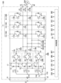
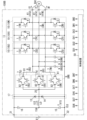
- FIG. 1 is a circuit diagram of a system including a power conversion device according to a first embodiment.
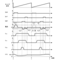
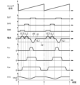
- FIG. 2 is an explanatory diagram of the operation when the control device performs the first control operation in the above power converter.
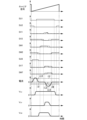
- FIG. 3 is another diagram illustrating the operation when the control device performs the first control operation in the power conversion device described above.
- FIG. 4 is an explanatory diagram of the operation of the control device in the above power converter.
- FIG. 5 is a diagram showing changes over time in duty corresponding to voltage commands for each of three phases in an AC load connected to a plurality of AC terminals of the power converter device.
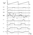
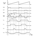
- FIG. 6 is a timing chart when the control device performs the second control operation in the power converter device as described above.
- FIG. 7 is a timing chart when the control device performs the third control operation in the above power conversion device.
- FIG. 8 is a circuit diagram of a system including the power conversion device according to the second embodiment.
- FIG. 9 is a timing chart when the control device performs the first control operation in the power conversion device same as above.
- FIG. 10 is a timing chart when the control device performs the second control operation in the power conversion device same as above.
- FIG. 11 is a timing chart showing another example when the control device performs the second control operation in the power conversion device same as above.
- FIG. 12 is a timing chart when the control device performs the third control operation in the power conversion device same as above.
- FIG. 13 is a timing chart showing another example when the control device performs the third control operation in the power converter device as described above.
- FIG. 9 is a timing chart when the control device performs the first control operation in the power conversion device same as above.
- FIG. 10 is a timing chart when the control device performs the second control operation in the power conversion
- FIG. 14 is a timing chart when the control device performs the second control operation in the power conversion device according to the third embodiment.
- FIG. 15 is a timing chart when the control device performs the third control operation in the power conversion device same as above.
- FIG. 16 is a timing chart when the control device performs the second control operation in the power conversion device according to the fourth embodiment.
- FIG. 17 is a timing chart when the control device performs the third operation in the power conversion device same as above.
- FIG. 18 is a timing chart when the control device performs the second control operation in the power conversion device according to the fifth embodiment.
- FIG. 19 is a timing chart when the control device performs the third control operation in the power conversion device same as above.
- FIG. 15 is a timing chart when the control device performs the third control operation in the power conversion device same as above.
- FIG. 16 is a timing chart when the control device performs the second control operation in the power conversion device according to the fourth embodiment.
- FIG. 17 is a timing chart when the control device performs the
- FIG. 20 is a timing chart when the control device performs the second control operation in the power conversion device according to the sixth embodiment.
- FIG. 21 is a timing chart when the control device performs the third control operation in the power conversion device same as above.
- FIG. 22 is a timing chart when the control device performs the second control operation in the power conversion device according to the seventh embodiment.
- FIG. 23 is a timing chart when the control device performs the third control operation in the power conversion device same as above.
- FIG. 24 is a circuit diagram of a system including a power conversion device according to Embodiment 8.
- FIG. 25 is a circuit diagram of a system including a power conversion device according to Embodiment 9.
- FIG. 26 is a circuit diagram of a system including a power conversion device according to Modification 1 of Embodiment 2.
- FIG. 21 is a timing chart when the control device performs the third control operation in the power conversion device same as above.
- FIG. 22 is a timing chart when the control device performs the second control operation in the
- FIG. 27 is a circuit diagram of a system including a power conversion device according to Modification 2 of Embodiment 2.
- FIG. 28 is a circuit diagram of a system including a power conversion device according to Modification 3 of Embodiment 2.
- FIG. 29 is a circuit diagram of a system including a power conversion device according to Modification 4 of Embodiment 2.
- FIG. 30 is a circuit diagram of a system including a power conversion device according to a fifth modification of the second embodiment.
- the power converter device 100 includes, for example, a first DC terminal 31, a second DC terminal 32, a plurality of (for example, three) AC terminals 41, A DC power source E1 is connected between the first DC terminal 31 and the second DC terminal 32, and an AC load RA1 is connected to the plurality of AC terminals 41.
- AC load RA1 is, for example, a three-phase motor.
- Power converter 100 converts DC output from DC power supply E1 into AC power and outputs it to AC load RA1.
- the DC power source E1 includes, for example, a solar cell or a fuel cell.
- the DC power supply E1 may include a DC-DC converter.
- the AC power is, for example, three-phase AC power having a U phase, a V phase, and a W phase.
- the power conversion device 100 includes a power conversion circuit 11, a plurality (for example, three) of bidirectional switches 8, a plurality of (for example, three) resonance capacitors 9, a regeneration capacitor 15, and a first resonance It includes an inductor L1, a second resonant inductor L2, a third resonant inductor L3, and a control device 50. Moreover, the power conversion device 100 further includes a plurality (three) of protection circuits 17 and a capacitor C10.
- the power conversion circuit 11 includes a plurality of (for example, three) first switching elements 1 and a plurality of (for example, three) second switching elements 2.
- a plurality of (for example, three) switching circuits 10 in which a plurality of first switching elements 1 and a plurality of second switching elements 2 are connected in series in a one-to-one manner are connected in parallel to each other.
- a plurality of first switching elements 1 are connected to a first DC terminal 31, and a plurality of second switching elements 2 are connected to a second DC terminal 32.
- the plurality of AC terminals 41 correspond to the plurality of switching circuits 10 on a one-to-one basis.
- Each of the plurality of AC terminals 41 is connected to a connection point 3 between the first switching element 1 and the second switching element 2 in the corresponding switching circuit 10.
- the plurality of bidirectional switches 8 correspond one-to-one to the plurality of switching circuits 10.
- Each of the plurality of bidirectional switches 8 has a first end 81 connected to a connection point 3 between the first switching element 1 and the second switching element 2 in the corresponding switching circuit 10.
- the plurality of resonance capacitors 9 correspond one-to-one to the plurality of bidirectional switches 8.
- Each of the plurality of resonance capacitors 9 is connected between the first end 81 of the corresponding bidirectional switch 8 and the second DC terminal 32.
- the regenerative capacitor 15 has a third end 153 and a fourth end 154, and the third end 153 is connected to the second DC terminal 32.
- the first resonant inductor L1, the second resonant inductor L2, and the third resonant inductor L3 are connected between the three bidirectional switches 8 and the fourth end 154 of the regenerative capacitor 15.
- the control device 50 controls the plurality of first switching elements 1, the plurality of second switching elements 2, and the plurality of bidirectional switches 8.
- the switching circuits 10 corresponding to the U phase, V phase, and W phase will be referred to as the switching circuit 10U, the switching circuit 10V, and the switching circuit, respectively. It is also sometimes referred to as 10W.
- the 1st switching element 1 and the 2nd switching element 2 of 10 U of switching circuits may be called 1 U of 1st switching elements, and 2 U of 2nd switching elements.
- the 1st switching element 1 and the 2nd switching element 2 of the switching circuit 10V may be called the 1st switching element 1V and the 2nd switching element 2V.
- the 1st switching element 1 and the 2nd switching element 2 of the switching circuit 10W may be called the 1st switching element 1W and the 2nd switching element 2W.
- the connection point 3 between the first switching element 1U and the second switching element 2U is referred to as the connection point 3U
- the connection point 3 between the first switching element 1V and the second switching element 2V is referred to as the connection point 3V
- the connection point 3 between the first switching element 1U and the second switching element 2V is referred to as the connection point 3V.
- the connection point 3 between the first switching element 1W and the second switching element 2W may be referred to as the connection point 3W.
- the AC terminal 41 connected to the connection point 3U will be referred to as an AC terminal 41U
- the AC terminal 41 connected to the connection point 3V will be referred to as an AC terminal 41V
- the AC terminal 41 connected to the connection point 3W will be referred to as an AC terminal 41V.
- the terminal 41 may also be referred to as an AC terminal 41W.
- the resonance capacitor 9 connected in parallel to the second switching element 2U will be referred to as a resonance capacitor 9U
- the resonance capacitor 9 connected in parallel to the second switching element 2V will be referred to as a resonance capacitor 9V.
- the resonance capacitor 9 connected in parallel to the second switching element 2W may also be referred to as a resonance capacitor 9W.
- bidirectional switch 8U first bidirectional switch 8U
- bidirectional switch 8V bidirectional switch 8V
- the bidirectional switch 8 connected to the connection point 3W may also be referred to as a bidirectional switch 8W (third bidirectional switch 8W).
- the high potential side output terminal (positive electrode) of the DC power source E1 is connected to the first DC terminal 31, and the low potential side output terminal (negative electrode) of the DC power source E1 is connected to the second DC terminal 32.
- the U phase, V phase, and W phase of the AC load RA1 are connected to three AC terminals 41U, 41V, and 41W, respectively.
- each of the plurality of (for example, three) first switching elements 1 and the plurality of (for example, three) second switching elements 2 has a control terminal, a first main terminal, and a second main terminal.
- Control terminals of the plurality of first switching elements 1 and the plurality of second switching elements 2 are connected to the control device 50.
- the first main terminal of the first switching element 1 is connected to the first DC terminal 31, and the second main terminal of the first switching element 1 is connected to the second switching element 2.
- the second main terminal of the second switching element 2 is connected to the second DC terminal 32 .
- the first switching element 1 is a high-side switching element (P-side switching element), and the second switching element 2 is a low-side switching element (N-side switching element).
- Each of the plurality of first switching elements 1 and the plurality of second switching elements 2 is, for example, an IGBT (Insulated Gate Bipolar Transistor). Therefore, the control terminal, first main terminal, and second main terminal of each of the plurality of first switching elements 1 and the plurality of second switching elements 2 are a gate terminal, a collector terminal, and an emitter terminal, respectively.
- the power conversion circuit 11 includes a plurality (three) of first diodes 4 connected one-to-one in antiparallel to a plurality (three) of first switching elements 1, and a plurality of (three) second switching elements 2. It further includes a plurality (three) of second diodes 5 that are connected one-to-one in antiparallel to each other.
- the anode of the first diode 4 is connected to the second main terminal (emitter terminal) of the first switching element 1 corresponding to this first diode 4
- the cathode of the first diode 4 is connected to the second main terminal (emitter terminal) of the first switching element 1 corresponding to the first diode 4.
- the anode of the second diode 5 is connected to the second main terminal (emitter terminal) of the second switching element 2 corresponding to this second diode 5
- the cathode of the second diode 5 is connected to the second main terminal (emitter terminal) of the second switching element 2 corresponding to the second diode 5. is connected to the first main terminal (collector terminal) of the second switching element 2 corresponding to this second diode 5.
- the U phase of the AC load RA1 is connected to the connection point 3U between the first switching element 1U and the second switching element 2U via the AC terminal 41U.
- the V phase of the AC load RA1 is connected to the connection point 3V between the first switching element 1V and the second switching element 2V via the AC terminal 41V.
- the W phase of the AC load RA1 is connected to the connection point 3W between the first switching element 1W and the second switching element 2W via the AC terminal 41W.
- the plurality of resonance capacitors 9 correspond one-to-one to the plurality of bidirectional switches 8. Each of the plurality of resonance capacitors 9 is connected between the first end 81 of the corresponding bidirectional switch 8 and the second DC terminal 32.
- Power conversion device 100 has a plurality of resonant circuits.
- the plurality of resonant circuits include a first resonant circuit having a resonant capacitor 9U and a first resonant inductor L1, a second resonant circuit having a resonant capacitor 9V and a second resonant inductor L2, and a resonant capacitor 9W. and a third resonant circuit having a third resonant inductor L3.
- Each of the plurality of bidirectional switches 8 includes, for example, two first IGBTs 6 and two second IGBTs 7 connected in antiparallel.
- the collector terminal of the first IGBT 6 and the emitter terminal of the second IGBT 7 are connected, and the emitter terminal of the first IGBT 6 and the collector terminal of the second IGBT 7 are connected.
- the emitter terminal of the first IGBT 6 is connected to the connection point 3 of the switching circuit 10 corresponding to the bidirectional switch 8 having the first IGBT 6.
- the collector terminal of the second IGBT 7 is connected to the connection point 3 of the switching circuit 10 corresponding to the bidirectional switch 8 having the second IGBT 7.
- the bidirectional switch 8U is connected to a connection point 3U between the first switching element 1U and the second switching element 2U.
- the bidirectional switch 8V is connected to the connection point 3V between the first switching element 1V and the second switching element 2V.
- the bidirectional switch 8W is connected to the connection point 3W between the first switching element 1W and the second switching element 2W.
- the first IGBT 6 and the second IGBT 7 of the bidirectional switch 8U will be referred to as the first IGBT 6U and the second IGBT 7U, respectively
- the first IGBT 6 and the second IGBT 7 of the bidirectional switch 8V will be referred to as the first IGBT 6V and the second IGBT 7V, respectively
- the first IGBT 6 and the second IGBT 7 of the bidirectional switch 8W may be referred to as a first IGBT 6W and a second IGBT 7W, respectively.
- the plurality of two-way switches 8 are controlled by a control device 50.
- the first IGBT 6U, the second IGBT 7U, the first IGBT 6V, the second IGBT 7V, the first IGBT 6W, and the second IGBT 7W are controlled by the control device 50.
- the regenerative capacitor 15 is connected between the first resonant inductor L1, the second resonant inductor L2, the third resonant inductor L3, and the second DC terminal 32.
- the regeneration capacitor 15 is, for example, a film capacitor.
- the first resonant inductor L1 is connected between the fourth end 154 of the regenerative capacitor 15 and the second end 82 of the bidirectional switch 8U.
- the second resonant inductor L2 is connected between the fourth end 154 of the regenerative capacitor 15 and the second end 82 of the bidirectional switch 8V.
- the third resonant inductor L3 is connected between the fourth end 154 of the regenerative capacitor 15 and the second end 82 of the bidirectional switch 8W.
- the power conversion device 100 includes a plurality (for example, three) of protection circuits 17 as described above.
- the plurality of protection circuits 17 are provided one each for the U phase, V phase, and W phase of AC load RA1.
- the plurality of protection circuits 17 are connected between the first DC terminal 31 and the second DC terminal 32.
- Each of the plurality of protection circuits 17 includes a third diode 13 and a fourth diode 14 connected in series to the third diode 13.
- the plurality of protection circuits 17 correspond one-to-one to the plurality of bidirectional switches 8.
- a connection point between the third diode 13 and the fourth diode 14 is connected to the second end 82 of the corresponding bidirectional switch 8.
- the anode of the third diode 13 is connected to the second end 82 of the bidirectional switch 8
- the cathode of the third diode 13 is connected to the first DC terminal 31.
- the fourth diode 14 the anode of the fourth diode 14 is connected to the second DC terminal 32, and the cathode of the fourth diode 14 is connected to the second end 82 of the bidirectional switch 8.
- Capacitor C10 is connected between the first DC terminal 31 and the second DC terminal 32, and is connected in parallel to the power conversion circuit 11.
- Capacitor C10 is, for example, an electrolytic capacitor.
- the control device 50 controls the plurality of first switching elements 1, the plurality of second switching elements 2, and the plurality of bidirectional switches 8.
- the execution body of the control device 50 includes a computer system.
- a computer system includes one or more computers.
- a computer system mainly consists of a processor and a memory as hardware.
- the function of the control device 50 as an execution entity in the present disclosure is realized by the processor executing a program recorded in the memory of the computer system.
- the program may be pre-recorded in the computer system's memory, or may be provided via a telecommunications line, or may be stored in a non-temporary storage device such as a memory card, optical disk, hard disk drive (magnetic disk), etc. that can be read by the computer system.
- a processor of a computer system is composed of one or more electronic circuits including a semiconductor integrated circuit (IC) or a large-scale integrated circuit (LSI).
- the plurality of electronic circuits may be integrated into one chip, or may be provided in a distributed manner over a plurality of chips.
- a plurality of chips may be integrated into one device, or may be distributed and provided in a plurality of devices.
- the control device 50 outputs PWM (Pulse Width Modulation) signals SU1, SV1, and SW1 that control on/off of the plurality of first switching elements 1U, 1V, and 1W, respectively.
- PWM Pulse Width Modulation
- Each of the PWM signals SU1, SV1, and SW1 has, for example, a first potential level (hereinafter also referred to as low level) and a second potential level higher than the first potential level (hereinafter also referred to as high level). ) is a signal that changes between.
- the first switching elements 1U, 1V, and 1W are turned on when the PWM signals SU1, SV1, and SW1 are at a high level, and turned off when they are at a low level.
- control device 50 outputs PWM signals SU2, SV2, and SW2 that control on/off of the plurality of second switching elements 2U, 2V, and 2W, respectively.
- Each of the PWM signals SU2, SV2, and SW2 has, for example, a first potential level (hereinafter also referred to as low level) and a second potential level higher than the first potential level (hereinafter also referred to as high level). ) is a signal that changes between.
- the second switching elements 2U, 2V, and 2W are turned on when the PWM signals SU2, SV2, and SW2 are at a high level, and turned off when they are at a low level.
- the control device 50 uses a sawtooth wave carrier signal (see FIG. 2) to generate PWM signals SU1, SV1, and SW1 corresponding to the plurality of first switching elements 1U, 1V, and 1W, respectively, and the plurality of second switching elements. PWM signals SU2, SV2, and SW2 corresponding to 2U, 2V, and 2W are generated. More specifically, the control device 50 generates PWM signals SU1 and SU2 to be applied to the first switching element 1U and the second switching element 2U, respectively, based on at least the carrier signal and the U-phase voltage command.
- control device 50 generates PWM signals SV1 and SV2 to be applied to the first switching element 1V and the second switching element 2V, respectively, based on at least the carrier signal and the V-phase voltage command. Further, the control device 50 generates PWM signals SW1 and SW2 to be applied to the first switching element 1W and the second switching element 2W, respectively, based on at least the carrier signal and the W-phase voltage command.
- the U-phase voltage command, the V-phase voltage command, and the W-phase voltage command are, for example, sinusoidal signals whose phases differ from each other by 120°, and the amplitudes (voltage command values) of each change with time.
- the length of one cycle of the U-phase voltage command, the V-phase voltage command, and the W-phase voltage command is the same. Further, the length of one cycle of the U-phase voltage command, the V-phase voltage command, and the W-phase voltage command is longer than the length of one cycle of the carrier signal.
- the control device 50 compares the U-phase voltage command and the carrier signal to generate a PWM signal SU1 to be applied to the first switching element 1U. Further, the control device 50 inverts the PWM signal SU1 applied to the first switching element 1U to generate a PWM signal SU2 applied to the second switching element 2U.
- control device 50 controls the period between the period when the PWM signal SU1 is at a high level and the period when the PWM signal SU2 is at a high level so that the on periods of the first switching element 1U and the second switching element 2U do not overlap.
- the dead time Td (see FIG. 2) is set to .
- the control device 50 compares the V-phase voltage command and the carrier signal to generate a PWM signal SV1 to be applied to the first switching element 1V. Further, the control device 50 inverts the PWM signal SV1 applied to the first switching element 1V to generate a PWM signal SV2 applied to the second switching element 2V.
- the control device 50 also controls the period between the period when the PWM signal SV1 is at a high level and the period when the PWM signal SV2 is at a high level so that the on periods of the first switching element 1V and the second switching element 2V do not overlap.
- the dead time Td (see FIG. 2) is set to .
- the control device 50 compares the W-phase voltage command and the carrier signal to generate a PWM signal SW1 to be applied to the first switching element 1W. Further, the control device 50 inverts the PWM signal SW1 applied to the first switching element 1W to generate a PWM signal SW2 applied to the second switching element 2W.
- the control device 50 also controls the period between the period when the PWM signal SW1 is at a high level and the period when the PWM signal SW2 is at a high level so that the on periods of the first switching element 1W and the second switching element 2W do not overlap.
- the dead time Td (see FIG. 3) is set to .
- the U-phase voltage command, the V-phase voltage command, and the W-phase voltage command are, for example, sinusoidal signals whose phases differ by 120 degrees from each other, and the amplitudes of each change with time. Therefore, the duty of the PWM signal SU1 (U-phase duty), the duty of the PWM signal SV1 (V-phase duty), and the duty of the PWM signal SW1 (W-phase duty) are, for example, as shown in FIG. °Changes in different sinusoidal shapes. Similarly, the duty of the PWM signal SU2, the duty of the PWM signal SV2, and the duty of the PWM signal SW2 change in the form of a sine wave whose phases are different from each other by 120°.
- the control device 50 generates each PWM signal SU1, SU2, SV1, SV2, SW1, SW2 based on the carrier signal, each voltage command, and information regarding the state of AC load RA1. For example, if the AC load RA1 is a three-phase motor, the information regarding the state of the AC load RA1 can be obtained from a plurality of Contains the detected value from the current sensor.
- the plurality of bidirectional switches 8, the first resonant inductor L1, the second resonant inductor L2, the third resonant inductor L3, the plurality of resonant capacitors 9, and the regenerative capacitor 15 are connected to the plurality of first switching elements 1 and the plurality of regenerative capacitors 15.
- the second switching element 2 is provided for zero-voltage soft switching.
- control device 50 also controls the plurality of bidirectional switches 8 in addition to the plurality of first switching elements 1 and second switching elements 2 of the power conversion circuit 11.
- the control device 50 generates control signals SU6, SU7, SV6, SV7, SW6, and SW7 that control on/off of the first IGBT 6U, the second IGBT 7U, the first IGBT 6V, the second IGBT 7V, the first IGBT 6W, and the second IGBT 7W. It outputs to the respective gate terminals of the 2 IGBT 7U, the first IGBT 6V, the second IGBT 7V, the first IGBT 6W, and the second IGBT 7W.
- the bidirectional switch 8U When the first IGBT 6U is on and the second IGBT 7U is off, the bidirectional switch 8U connects the regenerative capacitor 15 - the first resonant inductor L1 - the bidirectional switch 8U - the connection point 3U - the resonant capacitor 9U. A charging current flows through the capacitor and charges the resonance capacitor 9U.
- the bidirectional switch 8U connects the resonance capacitor 9U, the connection point 3U, the bidirectional switch 8U, the first resonance inductor L1, and the regeneration capacitor 15. A discharge current that flows through the resonant capacitor 9U and discharges the charge of the resonance capacitor 9U is passed.
- the bidirectional switch 8V When the first IGBT 6V is on and the second IGBT 7V is off, the bidirectional switch 8V connects the regeneration capacitor 15 - second resonance inductor L2 - bidirectional switch 8V - connection point 3V - resonance capacitor 9V. A charging current flows through the capacitor and charges the resonance capacitor 9V.
- the bidirectional switch 8V When the first IGBT 6V is off and the second IGBT 7V is on, the bidirectional switch 8V connects the resonance capacitor 9V - connection point 3V - bidirectional switch 8V - second resonance inductor L2 - regeneration capacitor 15. A discharge current flows through the capacitor and discharges the charge of the resonance capacitor 9V.
- the bidirectional switch 8W When the first IGBT 6W is on and the second IGBT 7W is off, the bidirectional switch 8W connects the regeneration capacitor 15 - third resonance inductor L3 - bidirectional switch 8W - connection point 3W - resonance capacitor 9W. A charging current flows through the capacitor and charges the resonance capacitor 9W.
- the bidirectional switch 8W connects the resonance capacitor 9W - connection point 3W - bidirectional switch 8W - third resonance inductor L3 - regeneration capacitor 15. A discharge current that flows through the resonant capacitor 9W and discharges the charge of the resonance capacitor 9W is passed.
- the first IGBT 6U of the bidirectional switch 8U is in the off state.
- the current iL1 flowing through the first resonant inductor L1 is regenerated to the power conversion circuit 11 via the third diode 13 until the energy of the first resonant inductor L1 is consumed and the current iL1 becomes zero.
- the second IGBT 7U may turn off from a state in which the second IGBT 7U of the bidirectional switch 8U is in the on state and the current iL1 is flowing in the first resonant inductor L1 with negative polarity. be.
- the current iL1 flowing through the first resonant inductor L1 flows through the fourth diode 14 - the first resonant inductor L1 - the regeneration capacitor until the energy of the first resonant inductor L1 is consumed and the current iL1 becomes zero. It flows through 15 routes.
- the first IGBT 6V of the bidirectional switch 8V is turned off.
- the condition may change.
- the current iL2 flowing through the second resonant inductor L2 is regenerated to the power conversion circuit 11 via the third diode 13 until the energy of the second resonant inductor L2 is consumed and the current iL2 becomes zero.
- the second IGBT 7V of the bidirectional switch 8V may be turned on from a state where the current iL2 is flowing in the second resonance inductor L2 with negative polarity, and then the second IGBT 7V may be turned off. be.
- the current iL2 flowing through the second resonant inductor L2 flows through the fourth diode 14 - the second resonant inductor L2 - the regeneration capacitor until the energy of the second resonant inductor L2 is consumed and the current iL2 becomes zero. It flows through 15 routes.
- the first IGBT 6W of the bidirectional switch 8W is turned off. condition may occur.
- the current iL3 flowing through the third resonant inductor L3 is regenerated to the power conversion circuit 11 via the third diode 13 until the energy of the third resonant inductor L3 is consumed and the current iL3 becomes zero.
- the second IGBT 7W of the bidirectional switch 8W may be in the on state and the current iL3 is flowing in the third resonance inductor L3 with negative polarity, and then the second IGBT 7W may be in the off state.
- the current iL3 flowing through the third resonant inductor L3 is changed from the fourth diode 14 to the third resonant inductor L3 to the regeneration capacitor 15 until the energy of the third resonant inductor L3 is consumed and the current iL3 becomes zero. flows along the route of
- the control device 50 controls the high level period of the PWM signals SU1, SV1, SW1 to the first switching elements 1U, 1V, 1W and the second switching elements 2U, 2V, 2V, A dead time Td is set between the high level periods of the PWM signals SU2, SV2, and SW2 to 2W. Further, in the first control operation, the high level period of the control signal to the bidirectional switch 8 corresponding to each of the plurality of switching circuits 10 among the plurality of bidirectional switches 8 overlaps with the dead time Td, and the high level period The start point of the dead time Td is advanced by an additional time than the start point of the dead time Td.
- the first control operation will be explained in more detail below.
- the control device 50 turns on the first IGBT 6 corresponding to the first switching element 1 to be subjected to zero voltage soft switching control. Thereby, the control device 50 causes the resonant inductor and the resonant capacitor 9 connected to the first switching element 1 to resonate, charges the resonant capacitor 9 from the regenerative capacitor 15, and charges the resonant capacitor 9 from the regenerative capacitor 15. Make the voltage at both ends zero.
- the resonance inductor is the first resonance inductor L1, the second resonance inductor L2, or the third resonance inductor L3.
- the control device 50 turns on the second IGBT 7 corresponding to the second switching element 2 to be subjected to zero voltage soft switching control.
- the control device 50 causes the resonant inductor and the resonant capacitor 9 connected to the second switching element 2 to resonate, and discharges from the resonant capacitor 9 to the regenerative capacitor 15, so that the resonant capacitor 9 is discharged from the resonant capacitor 9.
- the resonance capacitor 9 is charged and discharged via the bidirectional switch 8 so that the dead time Td described above and the half cycle of LC resonance ( ⁇ LC) are made to match.
- the power conversion device 100 can realize zero voltage soft switching.
- FIG. 2 shows PWM signals SU1 and SU2 applied from the control device 50 to the first switching element 1U and second switching element 2U of the switching circuit 10U, respectively.
- FIG. 2 also shows a control signal SU6 given from the control device 50 to the first IGBT 6U of the bidirectional switch 8U, an output current iU flowing to the U phase of the AC load RA1, and a current iL1 flowing to the first resonance inductor L1.
- a voltage V 1U across the first switching element 1U is illustrated.
- FIG. 2 shows PWM signals SV1 and SV2 applied from the control device 50 to the first switching element 1V and the second switching element 2V of the switching circuit 10V, respectively.
- FIG. 1 shows PWM signals SV1 and SV2 applied from the control device 50 to the first switching element 1V and the second switching element 2V of the switching circuit 10V, respectively.
- FIG. 2 also shows a control signal SV6 given from the control device 50 to the first IGBT 6V of the bidirectional switch 8V, an output current iV flowing to the V phase of the AC load RA1, and a current iL2 flowing to the second resonance inductor L2.
- a voltage V 1V across the first switching element 1V is illustrated.
- FIG. 2 illustrates a dead time Td that is set in the control device 50 to prevent the first switching element 1 and the second switching element 2 of the same phase from being turned on at the same time.
- FIG. 2 also shows an additional time Tau set for the control signal SU6 of the first IGBT 6U of the bidirectional switch 8U in the control device 50, and an additional time set for the control signal SV6 of the first IGBT 6V of the bidirectional switch 8V. Tav and are shown in the figure. Additional time Tau and additional time Tav will be described later.
- FIG. 3 shows PWM signals SW1 and SW2 applied from the control device 50 to the first switching element 1W and the second switching element 2W of the switching circuit 10W, respectively.
- FIG. 3 shows a control signal SW6 applied from the control device 50 to the first IGBT 6W of the bidirectional switch 8W, and an output current iW flowing into the W phase of the AC load RA1. Further, FIG. 3 shows a current iL3 flowing through the third resonant inductor L3. Further, FIG. 3 shows the voltage V 1W across the first switching element 1W.
- FIG. 3 shows a dead time Td set in the control device 50 to prevent the first switching element 1W and the second switching element 2W from being turned on at the same time. Further, FIG. 3 shows an additional time Taw set in the control device 50 with respect to the control signal SW6 of the first IGBT 6W of the bidirectional switch 8W. The additional time Taw will be described later.
- the above-mentioned additional time Tau is such that the start time t1 of the high level period of the control signal SU6 is earlier than the start time t2 of the dead time Td, so that the high level period of the control signal SU6 is earlier than the dead time Td. This is the time set to make it longer.
- the length of additional time Tau is set based on the value of output current iU. In order to start LC resonance from the start time t2 of the dead time Td, it is desirable that the value of the current iL1 match the value of the output current iU at the start time t2 of the dead time Td.
- the end point of the high-level period of the control signal SU6 may be the same as the end point t3 of the dead time Td or later.
- FIG. 2 shows an example in which the end point of the high level period of the control signal SU6 is set to be the same as the end point t3 of the dead time Td.
- the control device 50 sets the high level period of the control signal SU6 to Tau+Td.
- the voltage V 1U across the first switching element 1U becomes zero at the end time t3 of the dead time Td.
- the current iL1 flowing through the first resonant inductor L1 starts flowing at the start time t1 of the high level period of the control signal SU6, and at the time t4 when the additional time Tau has elapsed from the end time t3 of the dead time Td. becomes zero.
- the current iL1 at this time since iL1 ⁇ iU from the start time t2 of the dead time Td, the current iL1 in the shaded area of the current waveform in the fifth row from the top in FIG. 2 flows into the resonance capacitor 9U. LC resonance occurs.
- the current iL1 is regenerated to the power conversion circuit 11 via the third diode 13 that is directly connected to the first resonant inductor L1.
- the detection value at the carrier cycle to which the additional time Tau is added or at the timing closest to the carrier cycle is used. Further, as the estimated value of the output current iU at this time, a value obtained by estimating the output current iU in the carrier period to which the additional time Tau is added is used.
- FIG. 4 when the polarity of the output current iU is negative, the resonance capacitor 9U can be charged without turning on the first IGBT 6U of the bidirectional switch 8U. 1U zero voltage soft switching can be achieved.
- FIG. 4 also shows the voltage V 1U across the first switching element 1U and the voltage V 2U across the second switching element 2U. Further, FIG. 4 also shows the charging current of the resonance capacitor 9U.
- the above-mentioned additional time Tav is such that the high level period of the control signal SV6 is made earlier than the start time t6 of the dead time Td, so that the high level period of the control signal SV6 is earlier than the dead time Td. This is the time set to make it longer.
- the length of the additional time Tav is set based on the value of the output current iV. In order to start LC resonance from the start time t6 of the dead time Td, it is desirable that the value of the current iL2 match the value of the output current iV at the start time t6 of the dead time Td.
- the end point of the high level period of the control signal SV6 may be the same as the end time point t7 of the dead time Td or later.
- FIG. 2 shows an example in which the end point of the high level period of the control signal SV6 is set to be the same as the end point t7 of the dead time Td.
- the control device 50 sets the high level period of the control signal SV6 to Tav+Td.
- the voltage V 1V across the first switching element 1V becomes zero at the end time t7 of the dead time Td.
- the current iL2 flowing through the second resonant inductor L2 starts flowing at the start time t5 of the high level period of the control signal SV6, and at the time t8 when the additional time Tav has elapsed from the end time t7 of the dead time Td. becomes zero.
- the current iL2 at this time since iL2 ⁇ iV from the start time t6 of the dead time Td, the current iL2 in the shaded area with respect to the current waveform in the 10th row from the top in FIG. 2 flows into the resonance capacitor 9V. LC resonance occurs.
- the current iL2 is regenerated to the power conversion circuit 11 via the third diode 13 directly connected to the second resonant inductor L2 after the end time t7 of the dead time Td.
- a detection value at the carrier cycle to which the additional time Tav is added or at the timing closest to the carrier cycle is used.
- the estimated value of the output current iV at this time a value obtained by estimating the output current iV in the carrier cycle to which the additional time Tav is added is used.
- the resonance capacitor 9V can be charged without turning on the bidirectional switch 8V, and zero-voltage soft switching of the first switching element 1V can be realized.
- the above-mentioned additional time Taw is such that the start time t9 of the high level period of the control signal SW6 is earlier than the start time t10 of the dead time Td, so that the high level period of the control signal SW6 is made earlier than the dead time Td. This is the time set to make it longer.
- the length of the additional time Taw is set based on the value of the output current iW. In order to start LC resonance from the start time t10 of the dead time Td, it is desirable that the value of the current iL3 match the value of the output current iW at the start time t10 of the dead time Td.
- the end point of the high level period of the control signal SW6 may be the same as the end time point t11 of the dead time Td or later.
- FIG. 3 an example is shown in which the end point of the high level period of the control signal SW6 is set to be the same as the end time point t11 of the dead time Td.
- the control device 50 sets the high level period of the control signal SW6 to Taw+Td.
- the voltage V 1W across the first switching element 1W becomes zero at the end time t11 of the dead time Td.
- the current iL3 flowing through the third resonant inductor L3 starts flowing at the start time t9 of the high level period of the control signal SW6, and at the time t12 when the additional time Taw has elapsed from the end time t11 of the dead time Td. becomes zero.
- the current iL3 at this time since iL3 ⁇ iW from the start time t10 of the dead time Td, the current iL3 in the shaded area with respect to the current waveform in the fourth row from the top in FIG. 3 flows into the resonance capacitor 9W. LC resonance occurs.
- the current iL3 is regenerated to the power conversion circuit 11 via the third diode 13 directly connected to the third resonant inductor L3.
- the resonance capacitor 9W can be charged without turning on the bidirectional switch 8W, and zero-voltage soft switching of the first switching element 1W can be realized.
- the power converter 100 causes resonance capacitors 9 and resonance inductors associated with switching elements targeted for zero-voltage soft switching among the plurality of first switching elements 1 and the plurality of second switching elements 2 to resonate.
- the voltage across the resonant capacitor 9 related to the switching element targeted for zero-voltage soft switching changes according to the amplitude of the resonant voltage centered on the potential V15 of the fourth end 154 of the regenerative capacitor 15.
- the voltage across the switching element changes from the voltage value Vd (see FIGS. 2 and 3) of the DC power supply E1 applied between the first DC terminal 31 and the second DC terminal 32 to 0, so that it becomes zero. Voltage soft switching is realized.
- the potential V15 at the fourth end 154 of the regenerative capacitor 15 changes depending on the amount of charge or discharge of the regenerative capacitor 15 for each resonance between the resonant capacitor 9 and the resonant inductor. Further, the potential V15 at the fourth end 154 of the regenerative capacitor 15 changes depending on the amount of charge and discharge of the regenerative capacitor 15 for each carrier period.
- the amount of charged charge or the amount of discharged charge related to the output currents iU, iV, and iW of the U phase, V phase, and W phase is determined for each carrier cycle.
- the output currents iU, iV, and iW of each phase the current with the largest absolute value has the largest amount of charge.
- the output currents iU and iV of each phase are , iW are sinusoidal and have a phase difference of 120 degrees, so that charging and discharging in the regenerative capacitor 15 are balanced, and fluctuations in the potential V15 at the fourth end 154 of the regenerative capacitor 15 are suppressed.
- the control device 50 controls the high level period of the PWM signals SU1, SV1, SW1 to the first switching elements 1U, 1V, 1W and the second switching elements 2U, 2V, 2V, A dead time Td is set between the high level periods of the PWM signals SU2, SV2, and SW2 to 2W. Further, in the first control operation, the high level period of the control signal to the bidirectional switch 8 corresponding to each of the plurality of switching circuits 10 among the plurality of bidirectional switches 8 overlaps with the dead time Td, and the high level period The start point of the dead time Td is advanced by an additional time than the start point of the dead time Td.
- the control device 50 performs only the first control operation, for example, when the motor that is the AC load RA1 locks as a change in the state of the load, the output current of each phase will change. They end up with different constant values. Then, in the power conversion device 100, the difference between the potential V15 of the fourth end 154 of the regenerative capacitor 15 with respect to the ground potential and the half value (Vd/2) of the voltage value Vd of the DC power supply E1 becomes large.
- the resonant capacitors 9U, 9V, 9W and the first to third resonant inductors L1 to L3 resonate in order to realize zero voltage soft switching, the amplitude of the resonant voltage increases. There is a possibility that zero-voltage soft switching cannot be realized.
- control device 50 of the power conversion device 100 is configured to perform the following operations in addition to the above-described first control operation.
- the control device 50 acquires the detected potential of the potential V15 of the fourth end 154 of the regenerative capacitor 15 with respect to the ground potential. For example, the control device 50 acquires the detected potential every cycle of the carrier signal. For example, the control device 50 may store in advance the voltage value Vd of the DC voltage applied between the first DC terminal 31 and the second DC terminal 32, or may acquire the detection result of the voltage value Vd. You can. The control device 50 determines the content of the control operation based on the detected potential, the value of Vd/2, and the detection results of the output currents iU, iV, and iW.
- the control device 50 When the detected potential of the regenerative capacitor 15 is within the range from the first threshold Vth1 to the second threshold Vth2, the control device 50 performs the first control operation so that the detected potential of the regenerative capacitor 15 reaches the first threshold.
- the second control operation When the detected potential is smaller than Vth1, the second control operation is performed, and when the detected potential is larger than the second threshold Vth2, the third control operation is performed.
- the first threshold value Vth1 is smaller than Vd/2.
- the second threshold value Vth2 is larger than Vd/2.
- the first threshold value Vth1 is, for example, a value of 90% of Vd/2.
- the second threshold value Vth2 is, for example, a value of 110% of Vd/2.
- the second control operation is an operation of controlling the plurality of bidirectional switches 8 so as to increase the potential V15 at the fourth end 154 of the regenerative capacitor 15.
- the third control operation is an operation of controlling the plurality of bidirectional switches 8 so as to lower the potential V15 at the fourth end 154 of the regenerative capacitor 15.
- the first control operation is to overlap the high level period of the control signal to the bidirectional switch 8 corresponding to each of the plurality of switching circuits 10 among the plurality of bidirectional switches 8 with the dead time Td, and This is an operation that advances the start time of the high level period by an additional time than the start time of the dead time Td.
- the high level period of the control signal to the bidirectional switch 8U is the period when the potential level of the control signal SU6 to the first IGBT 6U is high level, or the period when the potential level of the control signal SU7 to the second IGBT 7U is high level.
- the high level period of the control signal to the bidirectional switch 8V is the period when the potential level of the control signal SV6 to the first IGBT 6V is high level, or the period when the potential level of the control signal SV7 to the second IGBT 7V is high level.
- the high level period of the control signal to the bidirectional switch 8W is the period when the potential level of the control signal SW6 to the first IGBT 6W is high level, or the period when the potential level of the control signal SW7 to the second IGBT 7W is high level.
- the additional time for making the high level period of the control signal to the bidirectional switch 8U earlier than the start time of the dead time Td is the above-mentioned additional time Tau.
- the additional time for making the high level period of the control signal to the bidirectional switch 8V earlier than the start of the dead time Td is the above-mentioned additional time Tav.
- the additional time for making the high-level period of the control signal to the bidirectional switch 8W earlier than the start time of the dead time Td is the above-mentioned additional time Taw.
- the second control operation is based on the polarity of each of the plurality of output currents iU, iV, and iW output from the plurality of AC terminals 41, so as to increase the potential V15 of the fourth end 154 of the regenerative capacitor 15. This is an operation to control the bidirectional switch 8.
- the third control operation is based on the polarity of each of the plurality of output currents iU, iV, and iW output from the plurality of AC terminals 41, so as to lower the potential V15 of the fourth end 154 of the regenerative capacitor 15. This is an operation to control the bidirectional switch 8.
- the control device 50 controls the discharge of the regenerative capacitor 15 of the plurality of bidirectional switches 8 based on the polarity of each of the plurality of output currents iU, iV, and iW output from the plurality of AC terminals 41.
- the high level period of the bidirectional switch 8 related to the operation is set to zero. An example of the operation at this time will be described with reference to FIG.
- FIG. 6 shows a carrier signal, control signals SU6, SV7, SW7, and multiple The output currents iU, iV, iW, the current iL1 flowing through the first resonant inductor L1, the current iL2 flowing through the second resonant inductor L2, and the current iL3 flowing through the third resonant inductor L3 are illustrated. be.
- FIG. 6 illustrates the voltages V 2U , V 2V , and V 2W across the second switching elements 2U, 2V , and 2W , respectively, and the potential V15 at the fourth end 154 of the regenerative capacitor 15.
- the voltages V 2U , V 2V , and V 2W across the second switching elements 2U, 2V , and 2W are the same as the voltages across the resonance capacitors 9U, 9V, and 9W, respectively.
- the timing at which the potential V15 of the fourth end 154 of the regenerative capacitor 15 is acquired for each carrier period is indicated by an arrow.
- the control device 50 selects a bidirectional switch related to the discharging operation of the regenerative capacitor 15 among the plurality of bidirectional switches 8 based on the polarity of each of the plurality of output currents iU, iV, and iW.
- the high level period of the control signal to 8 can be set to zero. As shown in FIG.
- the control device 50 acquires the detected potential of the potential V15 of the regenerative capacitor 15 every carrier cycle (at the timing of the upward arrow shown below the time axis in FIG. 6). , when the detected potential is smaller than the first threshold Vth1, the high level period of the control signal SU6 to the first IGBT 6U, which is related to the discharging operation of the regenerative capacitor 15, is set to zero. As a result, zero-voltage soft switching accompanied by a discharging operation of the regenerative capacitor 15 is not performed, so the potential V15 of the regenerative capacitor 15 in the next carrier cycle becomes larger than the first threshold value Vth1.
- Vth1 the high level period of the control signal SU6 to the first IGBT 6U
- the control signal SU6 and the corresponding current iL1 before the high level period is changed to zero are shown by two-dot chain lines.
- the high level period of the control signal SU6 to the first IGBT 6U becomes zero, as shown in FIG. 6, the voltage V 2U across the second switching element 2U rises steeply.
- zero voltage soft switching of the first switching element 1U is not performed and hard switching occurs, but the first switching element 1V and the first switching element 1W are subjected to zero voltage soft switching.
- the control device 50 charges the regenerative capacitor 15 of the plurality of bidirectional switches 8 based on the polarity of each of the plurality of output currents iU, iV, and iW output from the plurality of AC terminals 41.
- the high level period of the bidirectional switch 8 related to the operation is set to zero. An example of the operation at this time will be described with reference to FIG.
- the view of FIG. 7 is similar to that of FIG.
- the control device 50 selects a bidirectional switch related to the charging operation of the regenerative capacitor 15 among the plurality of bidirectional switches 8 based on the polarity of each of the plurality of output currents iU, iV, and iW.
- the high level period of the control signal to 8 can be set to zero. As shown in FIG.
- the control device 50 acquires the detected potential of the potential V15 of the regenerative capacitor 15 every carrier cycle, and when the detected potential is larger than the second threshold Vth2, the regenerative capacitor 15 is charged.
- the high level period of the control signal SU7 to the second IGBT 7U related to the operation is set to zero.
- zero-voltage soft switching accompanied by a charging operation of the regenerative capacitor 15 is not performed, so the potential V15 of the regenerative capacitor 15 in the next carrier cycle becomes smaller than the second threshold Vth2.
- the control signal SU7 and the corresponding current iL1 before the high level period is changed to zero are shown by two-dot chain lines.
- the control device 50 controls the high level period of the control signal to the bidirectional switch 8 corresponding to each of the plurality of switching circuits 10 among the plurality of bidirectional switches 8.
- a first control operation is performed to overlap the dead time Td and to bring the start point of the high level period earlier than the start point of the dead time Td by an additional time.
- the power conversion device 100 can realize zero-voltage soft switching of each of the plurality of first switching elements 1 and the plurality of second switching elements 2.
- control device 50 of the power conversion device 100 acquires the detected potential of the fourth end 154 of the regenerative capacitor 15 every carrier period, and when the detected potential is smaller than the first threshold Vth1 which is smaller than Vd/2, performs a second control operation to increase the potential V15 at the fourth end 154 of the regenerative capacitor 15, and when the detected potential is larger than the second threshold Vth2, which is larger than Vd/2, the regenerative capacitor 15 A third control operation is performed to lower the potential V15 at the fourth end 154 of the capacitor 15.
- the power conversion device 100 is able to suppress fluctuations in the potential V15 of the regenerative capacitor 15, and compared to the case where nothing is done to the fluctuations in the potential V15 of the regenerative capacitor 15, the power converter 100 is able to suppress fluctuations in the potential V15 of the regenerative capacitor 15.
- the ratio increases, resulting in improved power conversion efficiency and reduced noise.
- the control device 50 acquires the detected potential of the fourth end 154 of the regenerative capacitor 15 every cycle of the carrier signal.
- the second control operation is based on the polarity of each of the plurality of output currents iU, iV, and iW output from the plurality of AC terminals 41, so as to increase the potential V15 of the fourth end 154 of the regenerative capacitor 15. This is an operation to control the bidirectional switch 8.
- the third control operation is based on the polarity of each of the plurality of output currents iU, iV, and iW output from the plurality of AC terminals 41, so as to lower the potential V15 of the fourth end 154 of the regenerative capacitor 15. This is an operation to control the bidirectional switch 8. Therefore, the power conversion device 100 according to the first embodiment can more quickly suppress fluctuations in the potential at the fourth end 154 of the regenerative capacitor 15.
- the control device 50 in the power conversion device 100 controls the plurality of output currents iU, iV, and iW outputted from the plurality of AC terminals 41 based on the polarity of each
- the high level period of the control signal to the bidirectional switch 8 related to the discharging operation of the regenerative capacitor 15 is set to zero.
- the third control operation based on the polarity of each of the plurality of output currents iU, iV, and iW output from the plurality of AC terminals 41, one of the plurality of bidirectional switches 8 that is related to the charging operation of the regenerative capacitor 15 is selected.
- the high level period of the control signal to the direction switch 8 is set to zero. Therefore, the power conversion device 100 according to the first embodiment can perform the second control operation and the third control operation with a simple change from the first control operation.
- FIGS. 8 to 13 A power conversion device 100A according to the second embodiment will be described with reference to FIGS. 8 to 13.
- the same components as those in the power converter device 100 according to the first embodiment are given the same reference numerals, and the description thereof will be omitted.
- the first resonant inductor L1 and the second The resonance inductor L2 and the third resonance inductor L3 are composed of one resonance inductor L0. Therefore, in the power conversion device 100A, the resonant inductor L0 is a resonant inductor common to the plurality of resonant capacitors 9.
- a resonant circuit corresponding to the U phase is configured by the resonant inductor L0 and the resonant capacitor 9U
- a resonant circuit corresponding to the V phase is configured by the resonant inductor L0 and the resonant capacitor 9V
- a resonant circuit corresponding to the W phase is configured by the resonant inductor L0 and the resonant capacitor 9W.
- the resonant inductor L0 also serves as the first resonant inductor L1, the second resonant inductor L2, and the third resonant inductor L3, reducing the number of resonant inductors. be able to.
- the power conversion device 100A can also reduce the number of protection circuits 17.
- the plurality of bidirectional switches 8 correspond to the plurality of switching circuits 10 on a one-to-one basis.
- a first end 81 of each of the plurality of bidirectional switches 8 is connected to a connection point 3 between the first switching element 1 and the second switching element 2 in the switching circuit 10 corresponding to the bidirectional switch 8 .
- the second ends 82 of the plurality of bidirectional switches 8 are connected to one common connection point 25.
- the resonant inductor L0 has a first end and a second end. In the resonant inductor L0, the first end of the resonant inductor L0 is connected to the common connection point 25.
- the regenerative capacitor 15 is connected between the second end of the resonant inductor L0 and the second DC terminal 32.
- the control device 50 lengthens the respective high-level periods of the two control signals to the two bidirectional switches 8, and aligns the start and end points of the high-level periods of the two control signals.
- the control device 50 sets the high level period so that the dead time becomes ⁇ 2 times and the additional time becomes the sum of the additional time of the two phases. decide.
- the control device 50 performs control to shift at least one of the start time and end time of the high level period of each of the two control signals to the two bidirectional switches 8 corresponding to the two switching circuits 10. As a result, the start and end points of the high level periods of the two control signals to the two bidirectional switches 8 are made to coincide.
- the high-level period of each of the two control signals SV6 and SW6 is extended to overlap the entire two high-level periods.
- the previous PWM signals SV1, SV2, SW1, SW2 and control signals SV7, SW7 are shown by two-dot chain lines.
- the PWM signals SU1, SU2, SV1, SV2, SW1, SW2 and control signals when the high level period of each of the control signals SV7 and SW7 are extended and all of the two high level periods overlap each other are shown.
- Signals SU6, SV7, and SW7 are shown as solid lines.
- the current iL0 flowing during the high level period of the control signals SV7 and SW7 is shown by a chain double-dashed line before all of the control signals SV7 and SW7 are overlapped, and when all of the control signals SV7 and SW7 are overlapped,
- the current iL0 flowing in is shown by a solid line.
- the potential levels during the high level period are made different, but in reality, the potential level during the high level period is different. The potential levels of are the same.
- the control device 50 controls the discharge of the regenerative capacitor 15 of the plurality of bidirectional switches 8 based on the polarity of each of the plurality of output currents iU, iV, and iW output from the plurality of AC terminals 41.
- the high level period of the control signal to at least one of the two bidirectional switches 8 related to the operation is set to zero. An example of the operation at this time will be described with reference to FIGS. 10 and 11.
- the view of FIGS. 10 and 11 is similar to that of FIG.
- the control device 50 selects two of the plurality of bidirectional switches 8 that are related to the discharging operation of the regenerative capacitor 15 based on the polarity of each of the plurality of output currents iU, iV, and iW.
- the high level period of the control signal SV6 to one of the bidirectional switches 8V and 8W (bidirectional switch 8V) can be set to zero. As shown in FIG.
- the control device 50 acquires the detected potential of the potential V15 of the regenerative capacitor 15 every carrier cycle, and when the detected potential is smaller than the first threshold Vth1, the regenerative capacitor 15 is discharged.
- the high level period of the control signal SV6 to the first IGBT 6V related to the operation is set to zero, and the high level period of the control signal SW6 to the first IGBT 6W is shortened.
- the potential V15 of the regeneration capacitor 15 in the next carrier cycle becomes larger than the first threshold value Vth1.
- the control signal SV6 and the corresponding current iL0 before the high level period is changed to zero are shown by two-dot chain lines.
- the high level period of the control signals SV6 and SW6 to the first IGBTs 6V and 6W, which are related to the discharging operation of the regenerative capacitor 15, is set to zero.
- the potential V15 of the regeneration capacitor 15 in the next carrier cycle becomes larger than the first threshold value Vth1.
- the control device 50 charges the regenerative capacitor 15 of the plurality of bidirectional switches 8 based on the polarity of each of the plurality of output currents iU, iV, and iW output from the plurality of AC terminals 41.
- the high level period of the control signal to at least one of the two bidirectional switches 8 related to the operation is set to zero.
- An example of the operation at this time will be described with reference to FIGS. 12 and 13.
- the view of FIGS. 12 and 13 is similar to that of FIG.
- the control device 50 selects two of the plurality of bidirectional switches 8 that are related to the charging operation of the regenerative capacitor 15 based on the polarity of each of the plurality of output currents iU, iV, and iW.
- the high level period of the control signal SV7 to one of the bidirectional switches 8V and 8W (bidirectional switch 8V) can be set to zero. As shown in FIG.
- the control device 50 acquires the detected potential of the potential V15 of the regenerative capacitor 15 every carrier cycle, and when the detected potential is larger than the second threshold Vth2, the regenerative capacitor 15 is charged.
- the high level period of the control signal SV7 to the second IGBT 7V related to the operation is set to zero, and the high level period of the control signal SW7 to the second IGBT 7W is shortened.
- the potential V15 of the regeneration capacitor 15 in the next carrier period becomes smaller than the second threshold value Vth2.
- the control signal SV7 and the corresponding current iL0 before the high level period is changed to zero are shown by two-dot chain lines.
- the high level period of the control signals SV7 and SW7 to the second IGBTs 7V and 7W, which are related to the charging operation of the regenerative capacitor 15, is set to zero.
- the potential V15 of the regeneration capacitor 15 in the next carrier period becomes smaller than the second threshold value Vth2.
- the power conversion device 100A when the control device 50 determines that two-phase resonance currents flow simultaneously through the resonance inductor L0 while performing the first control operation, the two-phase resonance current flows simultaneously through the resonance inductor L0.
- the high level period of the control signal to each of the two bidirectional switches 8 through which the phase resonance current flows is lengthened to match the start and end points of the high level period of the two control signals.
- the power conversion device 100A can realize zero-voltage soft switching of each of the plurality of first switching elements 1 and the plurality of second switching elements 2 in a configuration in which the number of resonant inductors L0 is reduced to one. becomes.
- the control device 50 of the power converter 100A controls the discharging operation of the regenerative capacitor 15 among the plurality of bidirectional switches 8 based on the polarity of each of the plurality of output currents iU, iV, and iW.
- the high level period of the control signal to at least one of the two related bidirectional switches 8 is set to zero.
- the control device 50 controls two of the plurality of bidirectional switches 8 related to the charging operation of the regenerative capacitor 15 based on the polarity of each of the plurality of output currents iU, iV, and iW.
- the high level period of the control signal to at least one of the direction switches 8 is set to zero.
- the circuit configuration of the power conversion device 100 according to the third embodiment is the same as the power conversion device 100 according to the first embodiment (see FIG. 1), so illustration of the circuit diagram is omitted.
- the operation of the power conversion device 100 according to the third embodiment will be described below based on FIGS. 1, 14, and 15.
- the second control operation and the third control operation of the control device 50 are the same as the second control operation and the third control operation of the control device 50 of the power conversion device 100 according to the first embodiment. different.
- the control device 50 of the present embodiment selects both of the plurality of bidirectional switches 8 that are related to the discharging operation of the regenerative capacitor 15 based on the polarity of each of the plurality of output currents iU, iV, and iW.
- the period is shortened so that the integral value of the current flowing through the regenerative capacitor 15 in one period of the carrier signal becomes zero.
- FIG. 14 The view of FIG. 14 is similar to that of FIG.
- the control device 50 selects a bidirectional switch related to the discharging operation of the regenerative capacitor 15 among the plurality of bidirectional switches 8 based on the polarity of each of the plurality of output currents iU, iV, and iW.
- the high level period of the control signal SU6 to 8U is shortened. As shown in FIG.
- the control device 50 acquires the detected potential of the potential V15 of the regenerative capacitor 15 every carrier cycle, and when the detected potential is smaller than the first threshold Vth1, the regenerative capacitor 15 is discharged.
- the high level period of the control signal SU6 to the first IGBT 6U related to the operation is shortened. After the high level period of the control signal SU6 is shortened, the high level period of the control signal SU6 is longer than zero.
- the control device 50 of the present embodiment selects both of the plurality of bidirectional switches 8 that are related to the charging operation of the regenerative capacitor 15 based on the polarity of each of the plurality of output currents iU, iV, and iW.
- the control device 50 of the present embodiment selects both of the plurality of bidirectional switches 8 that are related to the charging operation of the regenerative capacitor 15 based on the polarity of each of the plurality of output currents iU, iV, and iW.
- the control device 50 selects a bidirectional switch related to the charging operation of the regenerative capacitor 15 among the plurality of bidirectional switches 8 based on the polarity of each of the plurality of output currents iU, iV, and iW.
- the high level period of the control signal SU7 to 8U is shortened. As shown in FIG.
- the control device 50 acquires the detected potential of the potential V15 of the regenerative capacitor 15 every carrier cycle, and when the detected potential is larger than the second threshold Vth2, the regenerative capacitor 15 is charged.
- the high level period of the control signal SU7 to the second IGBT 7U related to the operation is shortened to a period longer than zero. After the high level period of the control signal SU7 is shortened, the high level period of the control signal SU7 is longer than zero.
- the power conversion device 100 according to the third embodiment compared to the power conversion device 100 according to the first embodiment, it is possible to suppress ripples from occurring in the output current in the second control operation and the third control operation. Further, according to the power conversion device 100 according to the third embodiment, switching loss can be reduced in the second control operation and the third control operation compared to the power conversion device 100 according to the first embodiment, so that the power conversion efficiency can be further improved. It becomes possible to improve the performance.
- the circuit configuration of the power conversion device 100A according to the fourth embodiment is the same as that of the power conversion device 100A according to the second embodiment (see FIG. 8), so illustration of the circuit diagram is omitted.
- the operation of the power conversion device 100A according to the fourth embodiment will be described based on FIGS. 8, 16, and 17.
- the second control operation and the third control operation of the control device 50 are the same as the second control operation and the third control operation of the control device 50 of the power conversion device 100A according to the second embodiment. different.
- the control device 50 of the power conversion device 100A applies two-phase resonance corresponding to two switching circuits 10 among the plurality of switching circuits 10 to the resonance inductor L0 when performing the first control operation.
- the high level period of each of the two control signals to the two bidirectional switches 8 corresponding to the two switching circuits 10 among the plurality of bidirectional switches 8 is lengthened to generate two control signals.
- the start points and the end points of the high level periods of are aligned.
- the control device 50 of the present embodiment selects two of the plurality of bidirectional switches 8 related to the charging operation of the regenerative capacitor 15 based on the polarity of each of the plurality of output currents iU, iV, and iW.
- the high level period of the control signal to each of the two-way switches 8 is shortened. An example of the operation at this time will be described with reference to FIG. 16.
- the view of FIG. 16 is the same as that of FIG.
- the control device 50 selects a bidirectional switch related to the discharging operation of the regenerative capacitor 15 among the plurality of bidirectional switches 8 based on the polarity of each of the plurality of output currents iU, iV, and iW. Shorten the high level period of control signals SV6 and SW6 to 8V and 8W. As shown in FIG.
- the control device 50 acquires the detected potential of the potential V15 of the regenerative capacitor 15 every carrier cycle, and when the detected potential is smaller than the first threshold Vth1, the regenerative capacitor 15 is discharged.
- the high level period of the control signals SV6 and SW6 to the first IGBTs 6V and 6W related to the operation is shortened by the same amount of time.
- the shortened high level period of the control signals SV6 and SW6 is longer than zero.
- the control device 50 of the present embodiment selects two of the plurality of bidirectional switches 8 that are related to the charging operation of the regenerative capacitor 15 based on the polarity of each of the plurality of output currents iU, iV, and iW.
- the high level period of the control signal to each of the two-way switches 8 is shortened. An example of the operation at this time will be described with reference to FIG. 17.
- the view of FIG. 17 is the same as that of FIG.
- the control device 50 selects a bidirectional switch related to the charging operation of the regenerative capacitor 15 among the plurality of bidirectional switches 8 based on the polarity of each of the plurality of output currents iU, iV, and iW. Shorten the high level period of control signals SV7 and SW7 to 8V and 8W. As shown in FIG. 17,
- the control device 50 acquires the detected potential of the potential V15 of the regenerative capacitor 15 every carrier cycle, and when the detected potential is larger than the second threshold Vth2, the regenerative capacitor 15 is discharged.
- the high level period of the control signals SV7 and SW7 to the second IGBTs 7V and 7W related to the operation is shortened by the same amount of time.
- the shortened high level period of the control signals SV7 and SW7 is longer than zero.
- the power conversion device 100A according to the fourth embodiment compared to the power conversion device 100A according to the second embodiment, it is possible to suppress ripples from occurring in the output current in the second control operation and the third control operation. Moreover, according to the power conversion device 100A according to the fourth embodiment, switching loss can be reduced in the second control operation and the third control operation compared to the power conversion device 100A according to the second embodiment, so that the power conversion efficiency can be further improved. It becomes possible to improve the performance.
- the circuit configuration of the power conversion device 100 according to the fifth embodiment is the same as the power conversion device 100 according to the first embodiment (see FIG. 1), so illustration of the circuit diagram is omitted.
- the operation of the power conversion device 100 according to the fifth embodiment will be described based on FIGS. 1, 18, and 19.
- the second control operation and the third control operation of the control device 50 are the same as the second control operation and the third control operation of the control device 50 of the power conversion device 100 according to the first embodiment. different.
- the control device 50 of the present embodiment controls which of the plurality of bidirectional switches 8 related to the charging operation of the regenerative capacitor 15 based on the polarity of each of the plurality of output currents iU, iV, and iW.
- the control signal When extending the high level period of the control signal to the direction switch 8, the period is extended so that the integral value of the current flowing through the regenerative capacitor 15 becomes zero in one cycle of the carrier signal.
- the control device 50 selects a bidirectional switch related to the charging operation of the regenerative capacitor 15 among the plurality of bidirectional switches 8 based on the polarity of each of the plurality of output currents iU, iV, and iW.
- the control device 50 acquires the detected potential of the potential V15 of the regenerative capacitor 15 every carrier cycle, and when the detected potential is smaller than the first threshold Vth1, the regenerative capacitor 15 is charged.
- the high level period of the control signal SV7 to the second IGBT 7V related to the operation is extended. When extending the high level period of the control signal SV7, the control device 50 advances the start point of the high level period and delays the end point of the high level period.
- the control device 50 of the present embodiment selects both of the plurality of bidirectional switches 8 related to the discharging operation of the regenerative capacitor 15 based on the polarity of each of the plurality of output currents iU, iV, and iW.
- the control device 50 of the present embodiment selects both of the plurality of bidirectional switches 8 related to the discharging operation of the regenerative capacitor 15 based on the polarity of each of the plurality of output currents iU, iV, and iW.
- the control device 50 selects a bidirectional switch related to the discharging operation of the regenerative capacitor 15 among the plurality of bidirectional switches 8 based on the polarity of each of the plurality of output currents iU, iV, and iW.
- the control device 50 When extending the high level period of the control signal with the shortest high level period among the control signals to 8 (control signal SV6 in FIG. 19), the integral value of the current flowing through the regenerative capacitor 15 in one cycle of the carrier signal. Extend it so that it becomes zero. As shown in FIG. 19, the control device 50 acquires the detected potential of the potential V15 of the regenerative capacitor 15 every carrier period, and when the detected potential is larger than the second threshold Vth2, the regenerative capacitor 15 is discharged. The high level period of the control signal SV6 to the first IGBT 6V related to the operation is extended. When extending the high level period of the control signal SV6, the control device 50 advances the start time of the high level period and delays the end time of the high level period.
- the power conversion device 100 according to the fifth embodiment compared to the power conversion device 100 according to the first embodiment, it is possible to suppress ripples from occurring in the output current in the second control operation and the third control operation. Moreover, according to the power conversion device 100 according to the fifth embodiment, switching loss can be reduced in the second control operation and the third control operation compared to the power conversion device 100 according to the first embodiment, so that the power conversion efficiency can be further improved. It becomes possible to improve the performance.
- the circuit configuration of the power conversion device 100A according to the sixth embodiment is the same as the power conversion device 100A according to the second embodiment (see FIG. 8), so illustration of the circuit diagram is omitted.
- the operation of the power conversion device 100A according to the sixth embodiment will be described below based on FIGS. 8, 20, and 21.
- the second control operation and the third control operation of the control device 50 are the same as the second control operation and the third control operation of the control device 50 of the power conversion device 100A according to the second embodiment. different.
- the control device 50 of this embodiment determines that two-phase resonance currents corresponding to two switching circuits 10 among the plurality of switching circuits 10 simultaneously flow through the resonance inductor L0 when performing the first control operation. In this case, the high level period of each of the two control signals to the two bidirectional switches 8 corresponding to the two switching circuits 10 among the plurality of bidirectional switches 8 is lengthened, and the high level period of the two control signals is started. Match time points and end points.
- the control device 50 of this embodiment performs a regeneration operation in one period of the carrier signal when extending the high level period of the control signal to the two-way switch 8 different from the two-way switches 8. It is extended so that the integral value of the current flowing through the capacitor 15 becomes zero.
- FIG. 20 The view of FIG. 20 is the same as the view of FIG.
- the bidirectional switches 8U, 8V, and 8W are , related to the discharging operation, charging operation, and charging operation of the regenerative capacitor 15.
- the control device 50 acquires the detected potential of the potential V15 of the regenerative capacitor 15 every carrier cycle, and when the detected potential is smaller than the first threshold Vth1, repeats the high level period 2.
- the high level period of the control signal SU6 to the first IGBT 6U of the two-way switch 8U different from the two-way switches 8V and 8W is extended.
- the control device 50 advances the start time of the high level period.
- the control device 50 of this embodiment performs a regeneration operation in one period of the carrier signal when extending the high level period of the control signal to the two-way switch 8 different from the two-way switches 8. It is extended so that the integral value of the current flowing through the capacitor 15 becomes zero.
- FIG. 21 The view of FIG. 21 is the same as the view of FIG.
- the bidirectional switches 8U, 8V, and 8W are , relating to the charging operation, discharging operation, and discharging operation of the regenerative capacitor 15.
- the control device 50 acquires the detected potential of the potential V15 of the regenerative capacitor 15 every carrier period, and when the detected potential is larger than the second threshold Vth2, the high level period is overlapped 2.
- the high level period of the control signal SU7 to the second IGBT 7U of the two-way switch 8U different from the two-way switches 8V and 8W is extended. When extending the high level period, the start point of the high level period is brought forward.
- switching loss can be reduced in the second control operation and the third control operation compared to the power conversion device 100A according to the second embodiment, so that the power conversion efficiency is further improved. becomes possible.
- the second control operation and the third control operation of the control device 50 are the same as the second control operation and the third control operation of the control device 50 of the power conversion device 100 according to the first embodiment. different.
- the control device 50 controls the high level period of the PWM signals SU1, SV1, SW1 to the first switching element 1 and the PWM signals SU2, SV2 to the second switching element 2 for each of the plurality of switching circuits 10. , and the high level period of SW2.
- the high level period of the control signal to the bidirectional switch 8 corresponding to each of the plurality of switching circuits 10 among the plurality of bidirectional switches 8 overlaps with the dead time Td, and the start of the high level period is overlapped with the dead time Td. Advance the point in time by an additional amount of time before the start of the dead time.
- the control device 50 acquires the detected potential of the fourth end 154 of the regenerative capacitor 15 every cycle of the carrier signal, and when the detected potential is smaller than the first threshold Vth1, Based on the polarity of each of the output currents iU, iV, and iW, one bidirectional switch 8 among the plurality of bidirectional switches 8 has a high-level period that overlaps with the dead time Td in one cycle of the carrier signal.
- a control signal having a high level period related to the charging operation of the regenerative capacitor 15 is provided. An example of the operation at this time will be described with reference to FIG. 22.
- the view of FIG. 22 is the same as the view of FIG.
- the control device 50 acquires the detected potential of the potential V15 of the regenerative capacitor 15 every carrier cycle, and when the detected potential is smaller than the first threshold Vth1, the control device 50 applies the detected potential to the bidirectional switch 8U.
- a control signal SU7 having a high level period related to the charging operation of the regenerative capacitor 15 is provided separately from the control signal SU6 having a high level period overlapping the dead time Td.
- the control device 50 switches one of the plurality of bidirectional switches 8 based on the polarity of each of the plurality of output currents iU, iV, and iW.
- the control signal has a high level period related to the discharging operation of the regenerative capacitor 15. Give control signal. An example of the operation at this time will be described with reference to FIG. 23. The view of FIG. 23 is similar to that of FIG.
- the control device 50 acquires the detected potential of the potential V15 of the regenerative capacitor 15 every carrier cycle, and when the detected potential is smaller than the second threshold Vth2, the control device 50 applies the detected potential to the bidirectional switch 8U.
- a control signal SU6 having a high level period related to the discharging operation of the regenerative capacitor 15 is provided separately from the control signal SU7 having a high level period overlapping the dead time Td.
- the control device 50 sets the high level period of the control signal to the bidirectional switch 8 corresponding to each of the plurality of switching circuits 10 among the plurality of bidirectional switches 8 as a dead time Td.
- a first control operation is performed to overlap the dead time Td and to bring the start point of the high level period earlier than the start point of the dead time Td by an additional time.
- the power conversion device 100 can realize zero-voltage soft switching of each of the plurality of first switching elements 1 and the plurality of second switching elements 2.
- control device 50 of the power conversion device 100 acquires the detected potential of the fourth end 154 of the regenerative capacitor 15 every carrier period, and when the detected potential is smaller than the first threshold Vth1 which is smaller than Vd/2, performs a second control operation to increase the potential V15 at the fourth end 154 of the regenerative capacitor 15, and when the detected potential is larger than the second threshold Vth2, which is larger than Vd/2, the regenerative capacitor 15 A third control operation is performed to lower the potential V15 at the fourth end 154 of the capacitor 15.
- the power conversion device 100 is able to suppress fluctuations in the potential V15 of the regenerative capacitor 15, and compared to the case where nothing is done to the fluctuations in the potential V15 of the regenerative capacitor 15, the power converter 100 is able to suppress fluctuations in the potential V15 of the regenerative capacitor 15.
- the ratio increases, resulting in improved power conversion efficiency and reduced noise.
- the control device 50 acquires the detected potential of the fourth end 154 of the regenerative capacitor 15 every cycle of the carrier signal.
- the second control operation of the control device 50 is to increase the potential V15 of the fourth end 154 of the regenerative capacitor 15 based on the polarity of each of the plurality of output currents iU, iV, and iW output from the plurality of AC terminals 41. This is an operation for controlling a plurality of bidirectional switches 8 as shown in FIG.
- the third control operation of the control device 50 is to lower the potential V15 of the fourth end 154 of the regenerative capacitor 15 based on the polarity of each of the plurality of output currents iU, iV, and iW output from the plurality of AC terminals 41.
- This is an operation for controlling a plurality of bidirectional switches 8 as shown in FIG. Therefore, the power conversion device 100 according to the seventh embodiment can more quickly suppress fluctuations in the potential at the fourth end 154 of the regenerative capacitor 15.
- control device 50 in the power conversion device 100 according to the seventh embodiment only adds a control signal in both the second control operation and the third control operation compared to the case of the first control operation, the first control operation It becomes possible to implement the second control operation and the third control operation with a simple change from .
- the power converter 100B according to the eighth embodiment is different from the power converter 100A according to the second embodiment in that it further includes a capacitor 16 connected between the second end of the resonance inductor L0 and the first DC terminal 31. (See FIG. 8).
- the same components as those in the power conversion device 100A according to the second embodiment are denoted by the same reference numerals, and the description thereof will be omitted.
- the power conversion device 100B does not include the capacitor C10 in the power conversion device 100A according to the second embodiment.
- Capacitor 16 is connected in series to regenerative capacitor 15. Therefore, in the power conversion device 100B, a series circuit of the capacitor 16 and the regenerative capacitor 15 is connected between the first DC terminal 31 and the second DC terminal 32.
- the capacitance of the capacitor 16 is the same as that of the regenerative capacitor 15. "The capacitance of the capacitor 16 is the same as the capacitance of the regenerative capacitor 15" does not mean only when the capacitance of the capacitor 16 completely matches the capacitance of the regenerative capacitor 15; It may be within the range of 95% or more and 105% or less of the capacitance of the capacitor 15.
- the potential V15 at the fourth end 154 of the regenerative capacitor 15 is a value obtained by dividing the voltage value Vd of the DC power supply E1 by the capacitor 16 and the regenerative capacitor 15. Therefore, the potential V15 at the fourth end 154 of the regenerative capacitor 15 becomes Vd/2.
- the control device 50 may store in advance the value of the potential V15 at the fourth end 154 of the regenerative capacitor 15.
- the control device 50 of the power conversion device 100B according to the eighth embodiment performs the first control operation, the second control operation, and the third control operation similarly to the control device 50 of the power conversion device 100A according to the second embodiment. Therefore, the power conversion device 100B according to the eighth embodiment can improve power conversion efficiency like the power conversion device 100A according to the second embodiment.
- the power conversion device 100C according to the ninth embodiment is different from the power conversion device 100A according to the second embodiment in that the regeneration capacitor 15 is connected between the second end of the resonance inductor L0 and the first DC terminal 31. (See FIG. 8).
- the same components as those in the power converter device 100A according to the second embodiment are denoted by the same reference numerals, and the description thereof will be omitted.
- the control device 50 of the power conversion device 100C according to the ninth embodiment performs the first control operation, the second control operation, and the third control operation similarly to the control device 50 of the power conversion device 100A according to the second embodiment. Therefore, the power conversion device 100C according to the ninth embodiment can improve the power conversion efficiency like the power conversion device 100A according to the second embodiment.
- Embodiments 1 to 9 described above are only one of various embodiments of the present disclosure. Embodiments 1 to 9 described above can be modified in various ways depending on the design, etc., as long as the objective of the present disclosure can be achieved.
- each of the plurality of first switching elements 1 and the plurality of second switching elements 2 is not limited to an IGBT, but may be a MOSFET (Metal-Oxide-Semiconductor Field Effect Transistor).
- each of the plurality of first diodes 4 may be replaced by a parasitic diode or the like of a MOSFET that constitutes the corresponding first switching element 1.
- each of the plurality of second diodes 5 may be replaced by a parasitic diode of a MOSFET constituting the corresponding second switching element 2.
- the MOSFET is, for example, a Si-based MOSFET or a SiC-based MOSFET.
- Each of the plurality of first switching elements 1 and the plurality of second switching elements 2 may be, for example, a bipolar transistor or a GaN-based GIT (Gate Injection Transistor).
- each of the plurality of bidirectional switches 8 in the power conversion device 100A according to the second embodiment may have the configuration shown in any of the examples shown in FIGS. 26 to 30, for example.
- each of the plurality of bidirectional switches 8 in each of the plurality of bidirectional switches 8, the first IGBT 6 and the second IGBT 7 are connected in anti-series.
- the collector terminal of the first IGBT 6 and the collector terminal of the second IGBT 7 are connected, and the emitter terminal of the first IGBT 6 is one of the plurality of switching circuits 10. It is connected to the connection point 3 of the corresponding switching circuit 10, and the emitter of the second IGBT 7 is connected to the common connection point 25.
- Each of the plurality of bidirectional switches 8 further includes a diode 61 connected in anti-parallel to the first IGBT 6 and a diode 71 connected in anti-parallel to the second IGBT 7.
- each of the first IGBT 6 and the second IGBT 7 may be replaced with a MOSFET or a bipolar transistor.
- the diode 61 and the diode 71 in FIG. 26 may each be replaced by a parasitic diode of the replaced element, or an element built into one chip of the replaced element.
- the diode 61 and the diode 71 are not limited to being externally attached to the first IGBT 6 and the second IGBT 7, respectively, but may be elements built into one chip.
- each of the plurality of bidirectional switches 8 the first MOSFET 6A and the second MOSFET 7A are connected in anti-series.
- the drain terminal of the first MOSFET 6A and the drain terminal of the second MOSFET 7A are connected.
- Each of the plurality of bidirectional switches 8 further includes a diode 61 connected in antiparallel to the first MOSFET 6A, and a diode 71 connected in antiparallel to the second MOSFET 7A.
- the source terminal of the second MOSFET 7A is connected to the common connection point 25.
- the source terminal of the first MOSFET 6A is connected to the connection point 3 of the switching circuit 10 corresponding to the bidirectional switch 8 having the first MOSFET 6A.
- PWM signals SU1 and SU2 are applied from the control device 50 to the first MOSFET 6A and the second MOSFET 7A of the bidirectional switch 8U.
- PWM signals SV1 and SV2 are applied from the control device 50 to the first MOSFET 6A and the second MOSFET 7A of the bidirectional switch 8V.
- PWM signals SW1 and SW2 are applied from the control device 50 to the first MOSFET 6A and the second MOSFET 7A of the bidirectional switch 8W.
- a diode 63 is connected in series to the first MOSFET 6A, and a diode 73 is connected in series to the second MOSFET 7A.
- a series circuit of the first MOSFET 6A and the diode 63 and a series circuit of the second MOSFET 7A and the diode 73 are connected in antiparallel.
- each of the plurality of bidirectional switches 8 includes one MOSFET 80, a diode 83 connected in anti-parallel to the MOSFET 80, two diodes 84 connected in anti-parallel to the MOSFET 80, 85 in series, and two diodes 86 and 87 in series connected in antiparallel to MOSFET 80.
- the connection point between the diode 84 and the diode 85 in the bidirectional switch 8 (the first end 81 of the bidirectional switch 8 ) is connected to the corresponding one of the plurality of switching circuits 10 .
- connection point between the diode 86 and the diode 87 (the second end 82 of the bidirectional switch 8 ) is connected to the common connection point 25 .
- the bidirectional switch 8 is in the on state when the MOSFET 80 is in the on state, and the bidirectional switch 8 is in the off state when the MOSFET 80 is in the off state.
- the MOSFETs 80 of the plurality of bidirectional switches 8 are controlled by the control device 50.
- the control device 50 receives a control signal SU8 that controls on/off of the MOSFET 80 of the bidirectional switch 8U, a control signal SV8 that controls on/off of the MOSFET 80 of the bidirectional switch 8V, and a control signal that controls on/off of the MOSFET 80 of the bidirectional switch 8W. Outputs SW8.
- a resonant current flows through the resonant circuit including the resonant inductor L0 and the resonant capacitor 9 when the MOSFET 80 is in the on state.
- a charging current including a resonant current flows through the regenerative capacitor 15 - resonant inductor L0 - diode 86 - MOSFET 80 - diode. Flows through the path of 85-connection point 3-resonant capacitor 9.
- a discharge current including a resonance current flows through the resonance capacitor 9 - diode 84 - MOSFET 80 - diode 87 - resonance.
- the regenerative inductor L0 flows through the regenerative capacitor 15.
- each of the MOSFETs 80 may be replaced with an IGBT.
- each of the plurality of bidirectional switches 8 may include, for example, a bipolar transistor or a GaN-based GIT instead of the MOSFET 80.
- each of the plurality of bidirectional switches 8 is a dual gate type GaN-based GIT having a first source terminal, a first gate terminal, a second gate terminal, and a second source terminal.
- the control signal SU6 is applied between the first gate terminal and the first source terminal of the dual gate type GaN-based GIT that constitutes the bidirectional switch 8U, and the control signal SU6 is applied between the second gate terminal and the second source terminal.
- a control signal SU7 is provided.
- a control signal SV6 is applied between the first gate terminal and the first source terminal of the dual gate type GaN-based GIT that constitutes the bidirectional switch 8V, and a control signal SV7 is applied between the second gate terminal and the second source terminal.
- a control signal SW6 is applied between the first gate terminal and the first source terminal of the dual-gate type GaN-based GIT constituting the bidirectional switch 8W, and a control signal SW7 is applied between the second gate terminal and the second source terminal.
- each of the plurality of two-way switches 8 in Embodiments 1, 3 to 9 other than Embodiment 2 may have the configuration shown in any of the examples in FIGS. 26 to 30, for example.
- the power conversion devices 100, 100A, 100B, and 100C are not limited to a configuration that outputs three-phase AC, but may have a configuration that outputs polyphase AC of three or more phases.
- the power conversion device (100; 100A; 100B; 100C) includes a first DC terminal (31), a second DC terminal (32), a power conversion circuit (11), and a plurality of AC terminals ( 41), a plurality of bidirectional switches (8), a plurality of resonance capacitors (9), a regeneration capacitor (15), a first resonance inductor (L1), and a second resonance inductor (L2). , a third resonance inductor (L3), and a control device (50).
- the power conversion circuit (11) includes a plurality of first switching elements (1) and a plurality of second switching elements (2).
- a plurality of switching circuits (10) each having a plurality of first switching elements (1) and a plurality of second switching elements (2) connected in series in a one-to-one manner are connected in parallel to each other.
- a plurality of first switching elements (1) are connected to a first DC terminal (31), and a plurality of second switching elements (2) are connected to a second DC terminal (32). has been done.
- the plurality of AC terminals (41) correspond one-to-one to the plurality of switching circuits (10).
- Each of the plurality of AC terminals (41) is connected to a connection point (3) between the first switching element (1) and the second switching element (2) in the corresponding switching circuit (10).
- the plurality of bidirectional switches (8) correspond one-to-one to the plurality of switching circuits (10).
- Each of the plurality of bidirectional switches (8) has a first end (81) connected to a connection point (3) between the first switching element (1) and the second switching element (2) in the corresponding switching circuit (10). has been done.
- the plurality of resonance capacitors (9) correspond one-to-one to the plurality of bidirectional switches (8).
- Each of the plurality of resonance capacitors (9) is connected between the first end (81) of the corresponding bidirectional switch (8) and the second DC terminal (32).
- the regeneration capacitor (15) has a third end (153) and a fourth end (154).
- the regenerative capacitor (15) has a third end (153) connected to the first DC terminal (31) or the second DC terminal (32).
- the first resonant inductor (L1) is connected between the first bidirectional switch (bidirectional switch 8U) included in the plurality of bidirectional switches (8) and the fourth end (154) of the regenerative capacitor (15). It is connected.
- a second resonant inductor (L2) is connected between a second bidirectional switch (bidirectional switch 8V) included in the plurality of bidirectional switches (8) and a fourth end (154) of the regenerative capacitor (15). It is connected.
- the third resonant inductor (L3) is located between the third bidirectional switch (bidirectional switch 8W) included in the plurality of bidirectional switches (8) and the fourth end (154) of the regenerative capacitor (15). It is connected.
- the control device (50) supplies PWM signals (SU1, SV1) whose potentials change between high level and low level to each of the plurality of first switching elements (1) and the plurality of second switching elements (2). , SW1, SU2, SV2, SW2).
- the control device (50) performs a first control operation. In the first control operation, the high level period of the PWM signals (SU1, SV1, SW1) to the first switching element (1) and the PWM signal to the second switching element (2) for each of the plurality of switching circuits (10) are performed.
- a dead time (Td) is set between the high level period of (SU2, SV2, SW2).
- the high level period of the control signal to the bidirectional switch (8) corresponding to each of the plurality of switching circuits (10) among the plurality of bidirectional switches (8) is defined as a dead time (Td).
- the start time of the high level period is advanced by an additional time than the start time of the dead time (Td).
- the control device (50) acquires the detected potential of the fourth end (154) of the regenerative capacitor (15), and the detected potential is applied between the first DC terminal (31) and the second DC terminal (32). If the voltage is smaller than the first threshold (Vth1), which is smaller than half of the voltage value (Vd), a second control operation is performed to increase the potential at the fourth end (154) of the regenerative capacitor (15). .
- the control device (50) has a detection potential that is higher than a second threshold value (Vth2) that is larger than half of the voltage value (Vd) applied between the first DC terminal (31) and the second DC terminal (32). If the regenerative capacitor (15) is also large, a third control operation is performed to lower the potential at the fourth end (154) of the regenerative capacitor (15).
- the control device (50) controls the detected potential of the fourth end (154) of the regeneration capacitor (15). Acquired every cycle of the carrier signal.
- the second control operation is based on the polarity of each of the plurality of output currents (iU, iV, iW) output from the plurality of AC terminals (41), and the potential of the fourth end (154) of the regeneration capacitor (15).
- (V15) is an operation of controlling the plurality of bidirectional switches (8) to increase the voltage (V15).
- the third control operation is based on the polarity of each of the plurality of output currents (iU, iV, iW) output from the plurality of AC terminals (41).
- (V15) is an operation of controlling the plurality of bidirectional switches (8) to lower the voltage (V15).
- the power conversion device (100; 100A; 100B; 100C) according to the third aspect is based on the second aspect.
- the control device (50) controls the plurality of bidirectional switches (8) based on the polarity of each of the plurality of output currents (iU, iV, iW) output from the plurality of AC terminals (41).
- the high level period of the bidirectional switch (8) related to the discharging operation of the regenerative capacitor (15) is set to zero.
- the regenerative capacitor (15) of the plurality of bidirectional switches (8) is )
- the high level period of the bidirectional switch (8) related to the charging operation is set to zero.
- the first resonant inductor (L1), the second resonant inductor (L2), and the third resonant inductor (L3) is composed of one resonant inductor (L0).
- the control device (50) is performing the first control operation, two-phase resonance currents corresponding to two switching circuits (10) among the plurality of switching circuits (10) are applied to the resonance inductor (L0). If it is determined that the signals flow simultaneously, the high level period of each of the two control signals to the two bidirectional switches (8) corresponding to the two switching circuits (10) among the plurality of bidirectional switches (8) is lengthened.
- the start points and end points of the high level periods of the two control signals are aligned.
- the second control operation based on the polarity of each of the plurality of output currents (iU, iV, iW) outputted from the plurality of AC terminals (41), the The high level period of the control signal to at least one of the two bidirectional switches (8) related to the discharging operation of ) is set to zero.
- the regenerative capacitor (15) of the plurality of bidirectional switches (8) is )
- the high level period of the control signal to at least one of the two bidirectional switches (8) related to the charging operation of the battery is set to zero.
- the control device (50) is configured to output power from the plurality of AC terminals (41) in the second control operation. Based on the polarity of each of the plurality of output currents (iU, iV, iW), a control signal is sent to a bidirectional switch (8) related to the discharging operation of the regenerative capacitor (15) among the plurality of bidirectional switches (8).
- a bidirectional switch (8) related to the discharging operation of the regenerative capacitor (15) among the plurality of bidirectional switches (8).
- the regenerative capacitor (15) of the plurality of bidirectional switches (8) is ) When shortening the high-level period of the control signal to the bidirectional switch (8) related to the charging operation of Shorten to.
- switching loss can be reduced in the second control operation and the third control operation, so it is possible to further improve power conversion efficiency.
- the first resonant inductor (L1), the second resonant inductor (L2), and the third resonant inductor (L3) is composed of one resonant inductor (L0).
- the control device (50) is performing the first control operation, two-phase resonance currents corresponding to two switching circuits (10) among the plurality of switching circuits (10) are applied to the resonance inductor (L0). If it is determined that the signals flow simultaneously, the high level period of each of the two control signals to the two bidirectional switches (8) corresponding to the two switching circuits (10) among the plurality of bidirectional switches (8) is lengthened.
- the start points and end points of the high level periods of the two control signals are aligned.
- the high level period of the control signal to each of the two bidirectional switches (8) is shortened so that the integral value of the current flowing through the regeneration capacitor (15) in one period of the carrier signal becomes zero.
- the high level period of the control signal to each of the two bidirectional switches (8) is shortened so that the integral value of the current flowing through the regeneration capacitor (15) in one cycle of the carrier signal becomes zero. .
- the power conversion device (100; 100A; 100B; 100C) according to the seventh aspect is based on the second aspect.
- the control device (50) controls the plurality of bidirectional switches (8) based on the polarity of each of the plurality of output currents (iU, iV, iW) output from the plurality of AC terminals (41).
- the control signals to the bidirectional switch (8) related to the charging operation of the regenerative capacitor (15) when extending the high level period of the control signal with the shortest high level period, regeneration is performed in one cycle of the carrier signal. (15) so that the integral value of the current flowing through the capacitor (15) becomes zero.
- the regenerative capacitor (15) of the plurality of bidirectional switches (8) is ) flows to the regeneration capacitor (15) in one period of the carrier signal when extending the high level period of the control signal with the shortest high level period among the control signals to the bidirectional switch (8) related to the discharging operation of the carrier signal. Extend so that the integral value of the current becomes zero.
- switching loss can be reduced in the second control operation and the third control operation, so it is possible to further improve power conversion efficiency.
- the first resonant inductor (L1), the second resonant inductor (L2), and the third resonant inductor (L3) is composed of one resonant inductor (L0).
- the control device (50) is performing the first control operation, two-phase resonance currents corresponding to two switching circuits (10) among the plurality of switching circuits (10) are applied to the resonance inductor (L0). If it is determined that the signals flow simultaneously, the high level period of each of the two control signals to the two bidirectional switches (8) corresponding to the two switching circuits (10) among the plurality of bidirectional switches (8) is lengthened.
- the start points and end points of the high level periods of the two control signals are aligned.
- a bidirectional switch (8) different from the two bidirectional switches (8) is controlled so that the integral value of the current flowing through the regenerative capacitor (15) in one cycle of the carrier signal becomes zero. Extend the high level period of the signal.
- a bidirectional switch (8) different from the two bidirectional switches (8) is controlled so that the integral value of the current flowing through the regenerative capacitor (15) in one cycle of the carrier signal becomes zero. Extend the high level period of the signal.
- switching loss can be reduced in the second control operation and the third control operation, so it is possible to further improve power conversion efficiency.
- a power conversion device (100) includes a first DC terminal (31), a second DC terminal (32), a power conversion circuit (11), a plurality of AC terminals (41), and a plurality of AC terminals (41).
- the power conversion circuit (11) includes a plurality of first switching elements (1) and a plurality of second switching elements (2).
- a plurality of switching circuits (10) each having a plurality of first switching elements (1) and a plurality of second switching elements (2) connected in series in a one-to-one manner are connected in parallel to each other.
- a plurality of first switching elements (1) are connected to a first DC terminal (31), and a plurality of second switching elements (2) are connected to a second DC terminal (32). has been done.
- the plurality of AC terminals (41) correspond one-to-one to the plurality of switching circuits (10).
- Each of the plurality of AC terminals (41) is connected to a connection point (3) between the first switching element (1) and the second switching element (2) in the corresponding switching circuit (10).
- the plurality of bidirectional switches (8) correspond one-to-one to the plurality of switching circuits (10).
- Each of the plurality of bidirectional switches (8) has a first end (81) connected to a connection point (3) between the first switching element (1) and the second switching element (2) in the corresponding switching circuit (10). has been done.
- the plurality of resonance capacitors (9) correspond one-to-one to the plurality of bidirectional switches (8).
- Each of the plurality of resonance capacitors (9) is connected between the first end (81) of the corresponding bidirectional switch (8) and the second DC terminal (32).
- the regeneration capacitor (15) has a third end (153) and a fourth end (154).
- the regenerative capacitor (15) has a third end (153) connected to the first DC terminal (31) or the second DC terminal (32).
- the first resonant inductor (L1) is connected between the first bidirectional switch (bidirectional switch 8U) included in the plurality of bidirectional switches (8) and the fourth end (154) of the regenerative capacitor (15). It is connected.
- a second resonant inductor (L2) is connected between a second bidirectional switch (bidirectional switch 8V) included in the plurality of bidirectional switches (8) and a fourth end (154) of the regenerative capacitor (15). It is connected.
- the third resonant inductor (L3) is located between the third bidirectional switch (bidirectional switch 8W) included in the plurality of bidirectional switches (8) and the fourth end (154) of the regenerative capacitor (15). It is connected.
- the control device (50) supplies PWM signals (SU1, SU2) whose potential changes between high level and low level to each of the plurality of first switching elements (1) and the plurality of second switching elements (2). , SV1, SV2, SW1, SW2).
- the control device (50) performs a first control operation. In the first control operation, the high level period of the PWM signals (SU1, SV1, SW1) to the first switching element (1) and the PWM signal to the second switching element (2) for each of the plurality of switching circuits (10) are performed.
- a dead time (Td) is set between the high level period of (SU2, SV2, SW2).
- the high level period of the control signal to the bidirectional switch (8) corresponding to each of the plurality of switching circuits (10) among the plurality of bidirectional switches (8) overlaps with the dead time (Td). and the start time of the high level period is advanced by an additional time than the start time of the dead time (Td).
- the control device (50) acquires the detected potential of the fourth end (154) of the regenerative capacitor (15), and the detected potential is applied between the first DC terminal (31) and the second DC terminal (32).
- each of the plurality of output currents (iU, iV, iW) output from the plurality of AC terminals (41) Based on the polarity, a control signal having a high level period overlapping the dead time (Td) is sent to one bidirectional switch (8) among the plurality of bidirectional switches (8) in one cycle of the carrier signal. In addition to this, a second control operation is performed in which a control signal having a high level period related to the charging operation of the regenerative capacitor (15) is provided.
- the control device (50) has a detection potential that is higher than a second threshold value (Vth2) that is larger than half of the voltage value (Vd) applied between the first DC terminal (31) and the second DC terminal (32). is also large, one bidirectional switch among the plurality of bidirectional switches (8) is selected based on the polarity of each of the plurality of output currents (iU, iV, iW) output from the plurality of AC terminals (41).
- a high level period related to the discharging operation of the regenerative capacitor is provided.
- a third control operation is performed to provide a control signal having a value of .
Landscapes
- Engineering & Computer Science (AREA)
- Power Engineering (AREA)
- Inverter Devices (AREA)
Priority Applications (4)
| Application Number | Priority Date | Filing Date | Title |
|---|---|---|---|
| US18/877,068 US20250379527A1 (en) | 2022-07-08 | 2023-06-26 | Power converter |
| JP2024532044A JPWO2024009827A1 (https=) | 2022-07-08 | 2023-06-26 | |
| EP23835360.1A EP4554075A4 (en) | 2022-07-08 | 2023-06-26 | POWER CONVERTER |
| CN202380045727.9A CN119343862A (zh) | 2022-07-08 | 2023-06-26 | 电力转换器 |
Applications Claiming Priority (2)
| Application Number | Priority Date | Filing Date | Title |
|---|---|---|---|
| JP2022-110682 | 2022-07-08 | ||
| JP2022110682 | 2022-07-08 |
Publications (1)
| Publication Number | Publication Date |
|---|---|
| WO2024009827A1 true WO2024009827A1 (ja) | 2024-01-11 |
Family
ID=89453392
Family Applications (1)
| Application Number | Title | Priority Date | Filing Date |
|---|---|---|---|
| PCT/JP2023/023642 Ceased WO2024009827A1 (ja) | 2022-07-08 | 2023-06-26 | 電力変換装置 |
Country Status (5)
| Country | Link |
|---|---|
| US (1) | US20250379527A1 (https=) |
| EP (1) | EP4554075A4 (https=) |
| JP (1) | JPWO2024009827A1 (https=) |
| CN (1) | CN119343862A (https=) |
| WO (1) | WO2024009827A1 (https=) |
Cited By (3)
| Publication number | Priority date | Publication date | Assignee | Title |
|---|---|---|---|---|
| WO2025154526A1 (ja) * | 2024-01-19 | 2025-07-24 | パナソニックIpマネジメント株式会社 | 電力変換装置 |
| WO2025158857A1 (ja) * | 2024-01-26 | 2025-07-31 | パナソニックIpマネジメント株式会社 | 電力変換装置 |
| WO2025158856A1 (ja) * | 2024-01-22 | 2025-07-31 | パナソニックIpマネジメント株式会社 | 電力変換装置 |
Families Citing this family (1)
| Publication number | Priority date | Publication date | Assignee | Title |
|---|---|---|---|---|
| CN119496234A (zh) * | 2023-08-16 | 2025-02-21 | 台达电子企业管理(上海)有限公司 | 热插拔保护方法及供电装置 |
Citations (3)
| Publication number | Priority date | Publication date | Assignee | Title |
|---|---|---|---|---|
| JP2010233306A (ja) | 2009-03-26 | 2010-10-14 | Nissan Motor Co Ltd | 電力変換装置 |
| WO2020255459A1 (ja) * | 2019-06-18 | 2020-12-24 | 株式会社日立産機システム | 電力変換装置 |
| WO2023074636A1 (ja) * | 2021-10-26 | 2023-05-04 | パナソニックIpマネジメント株式会社 | 電力変換装置及び制御方法 |
Family Cites Families (3)
| Publication number | Priority date | Publication date | Assignee | Title |
|---|---|---|---|---|
| JP2000184738A (ja) * | 1998-12-15 | 2000-06-30 | Shihen Tech Corp | 部分共振pwmインバータ装置 |
| CN101383562B (zh) * | 2007-09-05 | 2011-03-30 | 力博特公司 | 一种开关电源中软开关电路的控制方法 |
| JP2011078204A (ja) * | 2009-09-30 | 2011-04-14 | Fuji Electric Systems Co Ltd | 電力変換装置及びその制御方法 |
-
2023
- 2023-06-26 JP JP2024532044A patent/JPWO2024009827A1/ja active Pending
- 2023-06-26 EP EP23835360.1A patent/EP4554075A4/en active Pending
- 2023-06-26 CN CN202380045727.9A patent/CN119343862A/zh active Pending
- 2023-06-26 WO PCT/JP2023/023642 patent/WO2024009827A1/ja not_active Ceased
- 2023-06-26 US US18/877,068 patent/US20250379527A1/en active Pending
Patent Citations (3)
| Publication number | Priority date | Publication date | Assignee | Title |
|---|---|---|---|---|
| JP2010233306A (ja) | 2009-03-26 | 2010-10-14 | Nissan Motor Co Ltd | 電力変換装置 |
| WO2020255459A1 (ja) * | 2019-06-18 | 2020-12-24 | 株式会社日立産機システム | 電力変換装置 |
| WO2023074636A1 (ja) * | 2021-10-26 | 2023-05-04 | パナソニックIpマネジメント株式会社 | 電力変換装置及び制御方法 |
Non-Patent Citations (1)
| Title |
|---|
| See also references of EP4554075A4 |
Cited By (3)
| Publication number | Priority date | Publication date | Assignee | Title |
|---|---|---|---|---|
| WO2025154526A1 (ja) * | 2024-01-19 | 2025-07-24 | パナソニックIpマネジメント株式会社 | 電力変換装置 |
| WO2025158856A1 (ja) * | 2024-01-22 | 2025-07-31 | パナソニックIpマネジメント株式会社 | 電力変換装置 |
| WO2025158857A1 (ja) * | 2024-01-26 | 2025-07-31 | パナソニックIpマネジメント株式会社 | 電力変換装置 |
Also Published As
| Publication number | Publication date |
|---|---|
| JPWO2024009827A1 (https=) | 2024-01-11 |
| CN119343862A (zh) | 2025-01-21 |
| EP4554075A4 (en) | 2025-10-15 |
| EP4554075A1 (en) | 2025-05-14 |
| US20250379527A1 (en) | 2025-12-11 |
Similar Documents
| Publication | Publication Date | Title |
|---|---|---|
| WO2023074636A1 (ja) | 電力変換装置及び制御方法 | |
| WO2024009827A1 (ja) | 電力変換装置 | |
| JP6369808B2 (ja) | 駆動装置、電力変換装置 | |
| JP6390959B2 (ja) | 駆動装置、電力変換装置 | |
| WO2024162289A1 (ja) | 電力変換装置 | |
| WO2024162204A1 (ja) | 電力変換装置 | |
| WO2024043125A1 (ja) | 電力変換装置 | |
| JP2018121473A (ja) | 電力変換装置 | |
| JPWO2018203422A1 (ja) | 半導体素子の駆動装置および電力変換装置 | |
| WO2024043124A1 (ja) | 電力変換装置 | |
| WO2023149193A1 (ja) | 電力変換装置 | |
| WO2024106290A1 (ja) | 電力変換装置 | |
| WO2025158856A1 (ja) | 電力変換装置 | |
| WO2025023007A1 (ja) | 電力変換装置 | |
| WO2025041615A1 (ja) | 電力変換装置 | |
| WO2025070009A1 (ja) | 電力変換装置 | |
| EP4704321A1 (en) | Electric power conversion apparatus | |
| WO2025070153A1 (ja) | 電力変換装置 | |
| US20260112979A1 (en) | Power converter | |
| WO2024106284A1 (ja) | 電力変換装置 | |
| WO2025154526A1 (ja) | 電力変換装置 | |
| JP2910518B2 (ja) | ブリッジ型インバ−タ装置 | |
| WO2025158857A1 (ja) | 電力変換装置 | |
| WO2024252787A1 (ja) | 電力変換装置 | |
| WO2024247827A1 (ja) | 電力変換装置 |
Legal Events
| Date | Code | Title | Description |
|---|---|---|---|
| 121 | Ep: the epo has been informed by wipo that ep was designated in this application |
Ref document number: 23835360 Country of ref document: EP Kind code of ref document: A1 |
|
| WWE | Wipo information: entry into national phase |
Ref document number: 202380045727.9 Country of ref document: CN |
|
| WWE | Wipo information: entry into national phase |
Ref document number: 2024532044 Country of ref document: JP |
|
| WWE | Wipo information: entry into national phase |
Ref document number: 18877068 Country of ref document: US |
|
| WWP | Wipo information: published in national office |
Ref document number: 202380045727.9 Country of ref document: CN |
|
| WWE | Wipo information: entry into national phase |
Ref document number: 2023835360 Country of ref document: EP |
|
| NENP | Non-entry into the national phase |
Ref country code: DE |
|
| ENP | Entry into the national phase |
Ref document number: 2023835360 Country of ref document: EP Effective date: 20250210 |
|
| WWP | Wipo information: published in national office |
Ref document number: 2023835360 Country of ref document: EP |
|
| WWP | Wipo information: published in national office |
Ref document number: 18877068 Country of ref document: US |