WO2024009737A1 - 蛍光検出装置 - Google Patents
蛍光検出装置 Download PDFInfo
- Publication number
- WO2024009737A1 WO2024009737A1 PCT/JP2023/022483 JP2023022483W WO2024009737A1 WO 2024009737 A1 WO2024009737 A1 WO 2024009737A1 JP 2023022483 W JP2023022483 W JP 2023022483W WO 2024009737 A1 WO2024009737 A1 WO 2024009737A1
- Authority
- WO
- WIPO (PCT)
- Prior art keywords
- liquid crystal
- crystal layer
- detection device
- fluorescence
- light
- Prior art date
- Legal status (The legal status is an assumption and is not a legal conclusion. Google has not performed a legal analysis and makes no representation as to the accuracy of the status listed.)
- Ceased
Links
Images





Classifications
-
- G—PHYSICS
- G01—MEASURING; TESTING
- G01N—INVESTIGATING OR ANALYSING MATERIALS BY DETERMINING THEIR CHEMICAL OR PHYSICAL PROPERTIES
- G01N21/00—Investigating or analysing materials by the use of optical means, i.e. using sub-millimetre waves, infrared, visible or ultraviolet light
- G01N21/62—Systems in which the material investigated is excited whereby it emits light or causes a change in wavelength of the incident light
- G01N21/63—Systems in which the material investigated is excited whereby it emits light or causes a change in wavelength of the incident light optically excited
- G01N21/64—Fluorescence; Phosphorescence
- G01N21/645—Specially adapted constructive features of fluorimeters
- G01N21/6456—Spatial resolved fluorescence measurements; Imaging
-
- G—PHYSICS
- G01—MEASURING; TESTING
- G01N—INVESTIGATING OR ANALYSING MATERIALS BY DETERMINING THEIR CHEMICAL OR PHYSICAL PROPERTIES
- G01N21/00—Investigating or analysing materials by the use of optical means, i.e. using sub-millimetre waves, infrared, visible or ultraviolet light
- G01N21/62—Systems in which the material investigated is excited whereby it emits light or causes a change in wavelength of the incident light
- G01N21/63—Systems in which the material investigated is excited whereby it emits light or causes a change in wavelength of the incident light optically excited
- G01N21/64—Fluorescence; Phosphorescence
- G01N21/645—Specially adapted constructive features of fluorimeters
-
- G—PHYSICS
- G02—OPTICS
- G02B—OPTICAL ELEMENTS, SYSTEMS OR APPARATUS
- G02B5/00—Optical elements other than lenses
- G02B5/30—Polarising elements
-
- G—PHYSICS
- G01—MEASURING; TESTING
- G01N—INVESTIGATING OR ANALYSING MATERIALS BY DETERMINING THEIR CHEMICAL OR PHYSICAL PROPERTIES
- G01N21/00—Investigating or analysing materials by the use of optical means, i.e. using sub-millimetre waves, infrared, visible or ultraviolet light
- G01N21/62—Systems in which the material investigated is excited whereby it emits light or causes a change in wavelength of the incident light
- G01N21/63—Systems in which the material investigated is excited whereby it emits light or causes a change in wavelength of the incident light optically excited
- G01N21/64—Fluorescence; Phosphorescence
- G01N21/645—Specially adapted constructive features of fluorimeters
- G01N2021/6463—Optics
Definitions
- the present disclosure relates to a fluorescence detection device.
- the fluorescence detection device of Patent Document 1 has an optical system having a dichroic mirror, and detects fluorescence reflected from a sample.
- the fluorescence detection device of Patent Document 1 does not require a dichroic mirror and is required to have further excitation light removal performance.
- An object of the present disclosure is to provide a fluorescence detection device with improved fluorescence detection sensitivity.
- a fluorescence detection device includes a light source that irradiates a sample with excitation light in a circularly polarized state, and a cholesteric liquid crystal layer that transmits fluorescence emitted by the sample by the excitation light and reflects the excitation light. , a detection circuit that detects the fluorescence transmitted through the cholesteric liquid crystal layer.
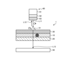
- FIG. 1 is a schematic diagram showing a fluorescence detection device according to Embodiment 1.
- FIG. 2 is a cross-sectional view schematically illustrating the cholesteric liquid crystal layer of Embodiment 1.
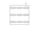
- FIG. 3 is a plan view schematically illustrating the first layer and the seventh layer of the cholesteric liquid crystal layer of Embodiment 1.
- FIG. 4 is a plan view schematically illustrating the second layer of the cholesteric liquid crystal layer of Embodiment 1.
- FIG. 5 is a plan view schematically illustrating the third layer of the cholesteric liquid crystal layer of Embodiment 1.
- FIG. 6 is a plan view schematically illustrating the fourth layer of the cholesteric liquid crystal layer of Embodiment 1.
- FIG. 1 is a schematic diagram showing a fluorescence detection device according to Embodiment 1.
- FIG. 2 is a cross-sectional view schematically illustrating the cholesteric liquid crystal layer of Embodiment 1.
- FIG. 3 is a plan view schematically
- FIG. 1 is a schematic diagram showing a fluorescence detection device according to Embodiment 1.
- FIG. 2 is a cross-sectional view schematically illustrating the cholesteric liquid crystal layer of Embodiment 1.
- FIG. 3 is a plan view schematically illustrating the first layer and the seventh layer of the cholesteric liquid crystal layer of Embodiment 1.
- FIG. 4 is a plan view schematically illustrating the second layer of the cholesteric liquid crystal layer of Embodiment 1.
- FIG. 5 is a plan view schematically illustrating the third layer of the cholesteric liquid crystal layer of Embodiment 1.
- FIG. 6 is a plan view schematically illustrating the fourth layer of the cholesteric liquid crystal layer of Embodiment 1.
- FIG. 1 is a schematic diagram showing a fluorescence detection device according to Embodiment 1.
- FIG. 2 is a cross-sectional view schematically illustrating the cholesteric liquid crystal layer of Embodiment 1.
- FIG. 3 is a plan view schematically
- the fluorescence detection device 1 includes a light source 60, a cholesteric liquid crystal layer 10, a transparent substrate 20, a sample holder 30, and a detection circuit 50 in a light-shielded space.
- the light-transmitting substrate 20 is an insulating base material, and for example, glass or resin material is used.
- the long axis directions of the liquid crystal molecules LC are aligned every 1/2 of the spiral pitch p, as shown in FIG. 3, the long axis direction of the liquid crystal molecules LC in the first layer LC1 and the liquid crystal molecules in the seventh layer LC7 The direction is the same as the long axis direction of LC.
- m is the reflection order
- ⁇ is the reflection wavelength
- p is the helical pitch
- n is the refractive index
- ⁇ is the angle formed by the incident direction of the excitation light with respect to the reflection surface BL.
- the sample holder 30 has translucency and places the sample 31 thereon.
- the sample holder 30 is preferably made of a transparent material that does not emit fluorescence, such as silicon nitride (SiN).
- the sample holding section 30 may be omitted.
- the detection circuit 50 is a charge coupled device and an imaging circuit.
- the detection circuit 50 can detect fluorescence intensity and fluorescence emission intensity distribution.
- the excitation light L11 incident from the light source 60 is selectively reflected as reflected light L12.
- the cholesteric liquid crystal layer 10 reflects right-handed circularly polarized light having a wavelength corresponding to the pitch p out of the excitation light L11, and uses it as reflected light L12.
- the cholesteric liquid crystal layer 10 reflects left-handed circularly polarized light having a wavelength corresponding to the pitch p out of the excitation light L11, and converts it into reflected light L12. do.
- the cholesteric liquid crystal layer 10 is manufactured by selecting a liquid crystal material and a chiral agent according to the wavelength of excitation light.
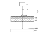
- FIG. 10 is a schematic diagram showing a fluorescence detection device according to a comparative example.
- the fluorescence detection device 1a of the comparative example shown in FIG. 10 does not have the cholesteric liquid crystal layer 10, as compared to the fluorescence detection device 1 shown in FIG.
- a sample holder 30 is stacked on a transparent substrate 20.
- the fluorescence detection device 1a of the comparative example when a sample 31 is irradiated with excitation light L21 of a predetermined wavelength, substances in the sample are excited and emit fluorescence having spectral characteristics whose peak wavelength is slightly shifted from the wavelength of the excitation light. .
- the fluorescence L22 containing the noise of the excitation light reaches the detection circuit 50.
- the cholesteric liquid crystal layer 10 selectively reflects the excitation light L11 as reflected light L12.
- the fluorescence detection device 1 of the first embodiment includes a light source 60 that irradiates the sample 31 with excitation light L11 in a circularly polarized state, a fluorescence L13 emitted by the sample 31 due to the excitation light L11, which transmits the fluorescence L13, It includes a cholesteric liquid crystal layer 10 that reflects excitation light L11, and a detection circuit that detects fluorescence L13 that has passed through the cholesteric liquid crystal layer 10.
- the excitation light L11 can be selectively reflected as reflected light L12, and the excitation light L11 reaching the detection circuit 50 is suppressed.
- the detection sensitivity of the fluorescence L13 detected by the detection circuit 50 is improved.
- FIG. 11 is a schematic diagram showing a fluorescence detection device according to Embodiment 2.
- the same components as those described in the above-described embodiments are denoted by the same reference numerals, and redundant description will be omitted.
- the fluorescence detection device 1A includes a light source 60, a cholesteric liquid crystal layer 10, a transparent substrate 20, a sample holder 30, and a detection circuit 50 in a light-shielded space.
- the light source 60 includes a light emitter 64 and a quarter wavelength plate 63.
- the light emitter 64 emits linearly polarized laser light.
- the quarter-wave plate 63 converts the light from the light emitter 64 into circularly polarized excitation light L11.
- FIG. 12 is a schematic diagram showing a fluorescence detection device according to Embodiment 3.
- the same components as those described in the above-described embodiments are denoted by the same reference numerals, and redundant description will be omitted.
- the fluorescence detection device 1B includes a light source 60, a cholesteric liquid crystal layer 10, a transparent substrate 20, a sample holder 30, a detection circuit 50, and a lens 70 in a light-shielded space. As shown in FIG. 12, the fluorescence detection device 1B according to the third embodiment further includes a lens 70 between the cholesteric liquid crystal layer 10 and the detection circuit 50 for condensing fluorescence from the sample 31.
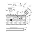
- FIG. 13 is a schematic diagram showing a fluorescence detection device according to Embodiment 4.
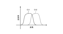
- FIG. 14 is an explanatory diagram showing the relationship between the wavelength characteristics of the excitation light reflected on the first liquid crystal layer and the wavelength characteristics of the excitation light reflected on the second liquid crystal layer in Embodiment 4.
- the same components as those described in the above-described embodiments are denoted by the same reference numerals, and redundant description will be omitted.
- the excitation light L11 incident from the light source 60 selectively becomes reflected light L12 and is reflected by the cholesteric liquid crystal layer 10, according to Bragg's law. Therefore, if the angle of incidence from the light source 60 deviates, the excitation light L11 will more easily enter the detection circuit 50.
- the fluorescence detection device 1C of the fourth embodiment has a plurality of liquid crystal layers with different reflection bands, so that the excitation light L11 can be reflected even if the incident angle of the excitation light L11 is slightly tilted. The guaranteed range of incident angles can be expanded.
- the fluorescence detection device 1C includes a light source 60, a cholesteric liquid crystal layer 10, a transparent substrate 20, a sample holding section 30, and a detection circuit 50 in a light-shielded space.
- the cholesteric liquid crystal layer 10 of the fourth embodiment includes a first liquid crystal layer 11 having a first helical pitch, and a second liquid crystal layer 12 having a second helical pitch different from the first pitch. include.
- the first liquid crystal layer 11 is formed on the alignment film 15 .
- the second liquid crystal layer 12 is formed on the first liquid crystal layer 11 .
- the first pitch of the helix of the first liquid crystal layer 11 and the second pitch of the helix of the second liquid crystal layer 12 are made different by changing the chiral agent or the like. As shown in FIG.
- the wavelength characteristic C11 of the excitation light reflected on the first liquid crystal layer 11 is shifted from the wavelength characteristic C12 of the excitation light reflected on the second liquid crystal layer 12.
- the cholesteric liquid crystal layer 10 may include three or more liquid crystal layers having different helical pitches.
- the first liquid crystal layer 11 cannot reflect the excitation light L11 of the light source 60A, but the second liquid crystal layer Layer 12 can reflect excitation light L11 from light source 60A.
Landscapes
- Health & Medical Sciences (AREA)
- Physics & Mathematics (AREA)
- General Physics & Mathematics (AREA)
- Biochemistry (AREA)
- Chemical & Material Sciences (AREA)
- Analytical Chemistry (AREA)
- Life Sciences & Earth Sciences (AREA)
- General Health & Medical Sciences (AREA)
- Nuclear Medicine, Radiotherapy & Molecular Imaging (AREA)
- Immunology (AREA)
- Pathology (AREA)
- Optics & Photonics (AREA)
- Investigating, Analyzing Materials By Fluorescence Or Luminescence (AREA)
Priority Applications (3)
| Application Number | Priority Date | Filing Date | Title |
|---|---|---|---|
| JP2024531996A JPWO2024009737A1 (https=) | 2022-07-07 | 2023-06-16 | |
| CN202380050353.XA CN119585606A (zh) | 2022-07-07 | 2023-06-16 | 荧光检测装置 |
| US19/007,588 US20250130168A1 (en) | 2022-07-07 | 2025-01-02 | Fluorescence detection device |
Applications Claiming Priority (2)
| Application Number | Priority Date | Filing Date | Title |
|---|---|---|---|
| JP2022110064 | 2022-07-07 | ||
| JP2022-110064 | 2022-07-07 |
Related Child Applications (1)
| Application Number | Title | Priority Date | Filing Date |
|---|---|---|---|
| US19/007,588 Continuation US20250130168A1 (en) | 2022-07-07 | 2025-01-02 | Fluorescence detection device |
Publications (1)
| Publication Number | Publication Date |
|---|---|
| WO2024009737A1 true WO2024009737A1 (ja) | 2024-01-11 |
Family
ID=89453236
Family Applications (1)
| Application Number | Title | Priority Date | Filing Date |
|---|---|---|---|
| PCT/JP2023/022483 Ceased WO2024009737A1 (ja) | 2022-07-07 | 2023-06-16 | 蛍光検出装置 |
Country Status (4)
| Country | Link |
|---|---|
| US (1) | US20250130168A1 (https=) |
| JP (1) | JPWO2024009737A1 (https=) |
| CN (1) | CN119585606A (https=) |
| WO (1) | WO2024009737A1 (https=) |
Citations (5)
| Publication number | Priority date | Publication date | Assignee | Title |
|---|---|---|---|---|
| JP2004004764A (ja) * | 2002-04-24 | 2004-01-08 | Nitto Denko Corp | 集光システムおよび透過型液晶表示装置 |
| US20110085219A1 (en) * | 2009-10-13 | 2011-04-14 | California Institute Of Technology | Holographically Illuminated Imaging Devices |
| US20120305801A1 (en) * | 2011-05-31 | 2012-12-06 | Samsung Electronics Co., Ltd. | Fluorescence detecting optical system and multi-channel fluorescence detection apparatus having the same |
| WO2020230556A1 (ja) * | 2019-05-10 | 2020-11-19 | 富士フイルム株式会社 | センサー |
| WO2020230698A1 (ja) * | 2019-05-10 | 2020-11-19 | 富士フイルム株式会社 | センサー |
-
2023
- 2023-06-16 CN CN202380050353.XA patent/CN119585606A/zh active Pending
- 2023-06-16 JP JP2024531996A patent/JPWO2024009737A1/ja active Pending
- 2023-06-16 WO PCT/JP2023/022483 patent/WO2024009737A1/ja not_active Ceased
-
2025
- 2025-01-02 US US19/007,588 patent/US20250130168A1/en active Pending
Patent Citations (5)
| Publication number | Priority date | Publication date | Assignee | Title |
|---|---|---|---|---|
| JP2004004764A (ja) * | 2002-04-24 | 2004-01-08 | Nitto Denko Corp | 集光システムおよび透過型液晶表示装置 |
| US20110085219A1 (en) * | 2009-10-13 | 2011-04-14 | California Institute Of Technology | Holographically Illuminated Imaging Devices |
| US20120305801A1 (en) * | 2011-05-31 | 2012-12-06 | Samsung Electronics Co., Ltd. | Fluorescence detecting optical system and multi-channel fluorescence detection apparatus having the same |
| WO2020230556A1 (ja) * | 2019-05-10 | 2020-11-19 | 富士フイルム株式会社 | センサー |
| WO2020230698A1 (ja) * | 2019-05-10 | 2020-11-19 | 富士フイルム株式会社 | センサー |
Also Published As
| Publication number | Publication date |
|---|---|
| CN119585606A (zh) | 2025-03-07 |
| JPWO2024009737A1 (https=) | 2024-01-11 |
| US20250130168A1 (en) | 2025-04-24 |
Similar Documents
| Publication | Publication Date | Title |
|---|---|---|
| JP7852112B2 (ja) | 光学素子および光偏向装置 | |
| JPWO2019131966A1 (ja) | 光学素子、導光素子および画像表示装置 | |
| JP6975258B2 (ja) | 光学素子およびセンサー | |
| JPWO2019189675A1 (ja) | 光偏向装置および光学装置 | |
| JPWO2020122128A1 (ja) | 導光素子、画像表示装置およびセンシング装置 | |
| JP2011123314A5 (https=) | ||
| JP7015392B2 (ja) | 光学素子およびセンサー | |
| CN112005139A (zh) | 光照射装置及传感器 | |
| JP7166445B2 (ja) | センサー | |
| CN116848454A (zh) | 虚像显示装置 | |
| US11988880B2 (en) | Optical coupling system and optical communication device | |
| WO2020226080A1 (ja) | 液晶回折素子および積層回折素子 | |
| JP6931417B2 (ja) | 光学素子 | |
| WO2021132630A1 (ja) | ハイパースペクトルセンサー、ハイパースペクトルカメラ | |
| US20250231111A1 (en) | Fluorescence detection device | |
| WO2024009737A1 (ja) | 蛍光検出装置 | |
| US20250138227A1 (en) | Optical element | |
| WO2023100916A1 (ja) | 光学素子および光学センサー | |
| JPWO2024009737A5 (https=) | ||
| WO2023101014A1 (ja) | ビームコンバイナ、配向膜の形成方法、および、光学素子の製造方法 | |
| WO2019172270A1 (ja) | 光学装置 | |
| JP7252355B2 (ja) | 光偏向装置および光学装置 | |
| US12571676B2 (en) | Spectroscope | |
| JPWO2024075814A5 (https=) | ||
| WO2021040012A1 (ja) | 光偏向装置および光学装置 |
Legal Events
| Date | Code | Title | Description |
|---|---|---|---|
| 121 | Ep: the epo has been informed by wipo that ep was designated in this application |
Ref document number: 23835271 Country of ref document: EP Kind code of ref document: A1 |
|
| WWE | Wipo information: entry into national phase |
Ref document number: 2024531996 Country of ref document: JP |
|
| WWE | Wipo information: entry into national phase |
Ref document number: 202380050353.X Country of ref document: CN |
|
| NENP | Non-entry into the national phase |
Ref country code: DE |
|
| WWP | Wipo information: published in national office |
Ref document number: 202380050353.X Country of ref document: CN |
|
| 122 | Ep: pct application non-entry in european phase |
Ref document number: 23835271 Country of ref document: EP Kind code of ref document: A1 |