WO2024005172A1 - 半導体装置及び電子機器 - Google Patents
半導体装置及び電子機器 Download PDFInfo
- Publication number
- WO2024005172A1 WO2024005172A1 PCT/JP2023/024297 JP2023024297W WO2024005172A1 WO 2024005172 A1 WO2024005172 A1 WO 2024005172A1 JP 2023024297 W JP2023024297 W JP 2023024297W WO 2024005172 A1 WO2024005172 A1 WO 2024005172A1
- Authority
- WO
- WIPO (PCT)
- Prior art keywords
- semiconductor chip
- bonding surface
- bonding
- semiconductor
- layer
- Prior art date
- Legal status (The legal status is an assumption and is not a legal conclusion. Google has not performed a legal analysis and makes no representation as to the accuracy of the status listed.)
- Ceased
Links
Images
















































Classifications
-
- H—ELECTRICITY
- H10—SEMICONDUCTOR DEVICES; ELECTRIC SOLID-STATE DEVICES NOT OTHERWISE PROVIDED FOR
- H10F—INORGANIC SEMICONDUCTOR DEVICES SENSITIVE TO INFRARED RADIATION, LIGHT, ELECTROMAGNETIC RADIATION OF SHORTER WAVELENGTH OR CORPUSCULAR RADIATION
- H10F39/00—Integrated devices, or assemblies of multiple devices, comprising at least one element covered by group H10F30/00, e.g. radiation detectors comprising photodiode arrays
- H10F39/80—Constructional details of image sensors
- H10F39/809—Constructional details of image sensors of hybrid image sensors
-
- H—ELECTRICITY
- H04—ELECTRIC COMMUNICATION TECHNIQUE
- H04N—PICTORIAL COMMUNICATION, e.g. TELEVISION
- H04N25/00—Circuitry of solid-state image sensors [SSIS]; Control thereof
- H04N25/70—SSIS architectures; Circuits associated therewith
-
- H—ELECTRICITY
- H10—SEMICONDUCTOR DEVICES; ELECTRIC SOLID-STATE DEVICES NOT OTHERWISE PROVIDED FOR
- H10F—INORGANIC SEMICONDUCTOR DEVICES SENSITIVE TO INFRARED RADIATION, LIGHT, ELECTROMAGNETIC RADIATION OF SHORTER WAVELENGTH OR CORPUSCULAR RADIATION
- H10F39/00—Integrated devices, or assemblies of multiple devices, comprising at least one element covered by group H10F30/00, e.g. radiation detectors comprising photodiode arrays
- H10F39/011—Manufacture or treatment of image sensors covered by group H10F39/12
- H10F39/028—Manufacture or treatment of image sensors covered by group H10F39/12 performed after manufacture of the image sensors, e.g. annealing, gettering of impurities, short-circuit elimination or recrystallisation
-
- H—ELECTRICITY
- H10—SEMICONDUCTOR DEVICES; ELECTRIC SOLID-STATE DEVICES NOT OTHERWISE PROVIDED FOR
- H10F—INORGANIC SEMICONDUCTOR DEVICES SENSITIVE TO INFRARED RADIATION, LIGHT, ELECTROMAGNETIC RADIATION OF SHORTER WAVELENGTH OR CORPUSCULAR RADIATION
- H10F39/00—Integrated devices, or assemblies of multiple devices, comprising at least one element covered by group H10F30/00, e.g. radiation detectors comprising photodiode arrays
- H10F39/80—Constructional details of image sensors
- H10F39/811—Interconnections
-
- H—ELECTRICITY
- H10—SEMICONDUCTOR DEVICES; ELECTRIC SOLID-STATE DEVICES NOT OTHERWISE PROVIDED FOR
- H10W—GENERIC PACKAGES, INTERCONNECTIONS, CONNECTORS OR OTHER CONSTRUCTIONAL DETAILS OF DEVICES COVERED BY CLASS H10
- H10W42/00—Arrangements for protection of devices
- H10W42/121—Arrangements for protection of devices protecting against mechanical damage
Definitions
- the present technology (technology according to the present disclosure) relates to semiconductor devices and electronic devices, and in particular, relates to a technology that is effective when applied to semiconductor devices having a semiconductor chip directly bonded to a base member and electronic devices equipped with the same. be.
- Photodetection devices such as solid-state imaging devices and distance measuring devices are known as semiconductor devices.
- This photodetecting device employs a three-dimensional structure in order to achieve miniaturization and high pixel density.
- a known method for realizing a three-dimensional structure is to directly bond two semiconductor wafers.
- Patent Document 1 discloses a technique for suppressing warpage caused by bonding substrates.
- chip bonding method in which a square semiconductor chip is directly bonded to a base member (bonding member) such as a semiconductor wafer or a semiconductor chip.
- bonding member such as a semiconductor wafer or a semiconductor chip.
- the outer periphery of the semiconductor chip may be lifted off the base member due to warping of the semiconductor chip, making it easy to cause defects such as cracking or chipping of the semiconductor chip, so it is difficult to manufacture semiconductor devices. This causes a decrease in yield.
- the thickness of the substrate of the semiconductor chip may be reduced after the semiconductor chip is directly bonded to the base member.
- the rigidity of the semiconductor chip becomes weak and the semiconductor chip is likely to float.
- the purpose of this technology is to improve manufacturing yield.
- a semiconductor device includes a base member having a first bonding surface and a semiconductor chip having a rectangular second bonding surface.
- the second bonding surface of the semiconductor chip and the first bonding surface of the base member are directly bonded.
- the semiconductor chip includes a multilayer wiring layer including the second bonding surface, and a semiconductor layer provided on a side of the multilayer wiring layer opposite to the second bonding surface.
- the multilayer wiring layer includes a warpage suppressing film extending along at least one side of the second bonding surface and suppressing warping of the semiconductor chip.
- a semiconductor device includes: a base member having a first joint surface; a semiconductor chip having a rectangular second bonding surface, the second bonding surface being directly bonded to the first bonding surface of the base member; Equipped with The above semiconductor chip is a multilayer wiring layer including the second bonding surface; a semiconductor layer provided on a side opposite to the second bonding surface side of the multilayer wiring layer; a warpage suppressing section provided in the multilayer wiring layer and suppressing warping of the semiconductor chip; Equipped with The warp suppressing portion is selectively provided on the peripheral edge side of the second bonding surface in plan view.
- a semiconductor device includes: a base member having a first joint surface; a semiconductor chip having a rectangular second bonding surface, the second bonding surface being directly bonded to the first bonding surface of the base member; Equipped with The above semiconductor chip is a multilayer wiring layer including the second bonding surface; a semiconductor layer provided on a side opposite to the second bonding surface side of the multilayer wiring layer and having a rectangular back surface on the opposite side to the multilayer wiring layer side; a warpage suppressing part provided in the semiconductor layer and suppressing warpage of the semiconductor chip; Equipped with The warpage suppressing portion is selectively provided on the peripheral edge side of the back surface of the semiconductor layer in plan view.
- a semiconductor device includes: a base member having a first joint surface; a semiconductor chip having a rectangular second bonding surface, the second bonding surface being directly bonded to the first bonding surface of the base member; Equipped with The above semiconductor chip is a multilayer wiring layer including the second bonding surface; a semiconductor layer provided on a side opposite to the second bonding surface side of the multilayer wiring layer; Equipped with The second bonding surface includes an insulating layer included in the multilayer wiring layer and a weak bonding portion having a weaker bonding force with the first bonding surface than with the insulating layer, The weak joint portion is provided on the peripheral edge side of the second joint surface.
- a semiconductor device includes: a base member having a rectangular first joint surface; a semiconductor chip having a rectangular second bonding surface, the second bonding surface being directly bonded to the first bonding surface of the base member; Equipped with At least one of the first bonding surface and the second bonding surface includes a weak bonding region and a strong bonding region having relatively different bonding forces with the other bonding surface, and The region is provided on the peripheral edge side of one joint surface.
- An electronic device includes the semiconductor device, an optical system that forms image light from a subject on the semiconductor device, and a signal processing method for a signal output from the semiconductor device. and a signal processing circuit for performing the processing.
- FIG. 1 is a block diagram illustrating a configuration example of a solid-state imaging device according to a first embodiment of the present technology.
- FIG. 2 is an equivalent circuit diagram showing a configuration example of a pixel and a pixel circuit of a solid-state imaging device according to a first embodiment of the present technology.
- FIG. 1 is a plan layout diagram schematically showing a configuration example of a solid-state imaging device according to a first embodiment of the present technology.
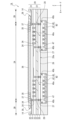
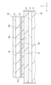
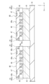
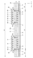
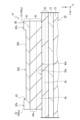
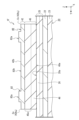
- FIG. 2 is a vertical cross-sectional view schematically showing a vertical cross-sectional structure along the a3-a3 cutting line in FIG. 1.
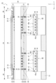
- FIG. 5 is a developed view of FIG. 4.
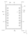
- FIG. 4 is a bottom view schematically showing the bottom side of the solid-state imaging device of FIG. 3.
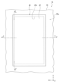
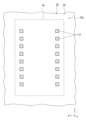
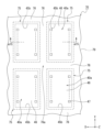
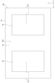
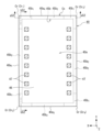
- FIG. 3 is a plan view schematically showing a state in which a second semiconductor chip is bonded to a first semiconductor chip when viewed from the second semiconductor chip side, with illustration of a sealing body omitted;
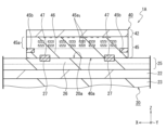
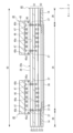
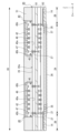
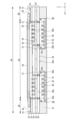
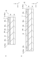
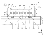
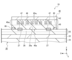
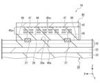
- FIG. 8 is a vertical cross-sectional view schematically showing the vertical cross-sectional structure along section line a7-a7 in FIG. 7; 8 is a vertical cross-sectional view schematically showing a vertical cross-sectional structure taken along the b7-b7 cutting line in FIG. 7.
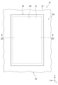
- FIG. FIG. 3 is a plan view schematically showing the bonding surface side of the first semiconductor chip.
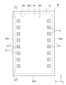
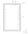
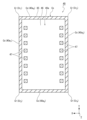
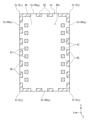
- FIG. 3 is a plan view schematically showing the bonding surface side of the second semiconductor chip.
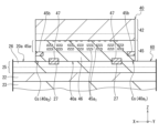
- FIG. 16 is a vertical cross-sectional view schematically showing a vertical cross-sectional structure taken along the a15-a15 cutting line in FIG. 15.
- FIG. FIG. 6 is a plan view schematically showing a state in which a dicing process is performed on a semiconductor wafer in the second semiconductor chip manufacturing method.
- FIG. 18 is a vertical cross-sectional view schematically showing a vertical cross-sectional structure taken along the cutting line a17-a17 in FIG. 17.
- FIG. 7 is a vertical cross-sectional view schematically showing a state in which a ring CMP step is performed in the second semiconductor chip manufacturing method.
- FIG. 7 is a process cross-sectional view schematically showing the formation of a warpage suppressing film and a bonding metal pad in the second semiconductor chip manufacturing method.
- FIG. 7 is a process cross-sectional view schematically showing the formation of a warpage suppressing film and a bonding metal pad in the second semiconductor chip manufacturing method.
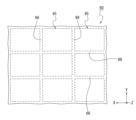
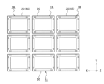
- FIG. 2 is a plan view schematically showing a wafer stack for explaining a method for manufacturing a first semiconductor chip included in a solid-state imaging device according to a first embodiment of the present technology.
- FIG. 23 is a vertical cross-sectional view schematically showing the vertical cross-sectional structure of the wafer stack shown in FIG. 22;
- FIG. 23 is an enlarged view of region B in FIG. 22 showing the configuration of a chip forming region.
- FIG. 1 is a plan view schematically showing steps of a method for manufacturing a solid-state imaging device according to a first embodiment of the present technology.
- FIG. 26 is a vertical cross-sectional view schematically showing a vertical cross-sectional structure taken along the a25-a25 cutting line in FIG. 25.
- FIG. 26 is a plan view schematically showing a step subsequent to FIG. 25.
- FIG. FIG. 28 is a vertical cross-sectional view schematically showing a vertical cross-sectional structure taken along the cutting line a27-a27 in FIG. 27.
- FIG. 29 is an enlarged vertical cross-sectional view of a part of FIG. 28;
- FIG. 28 is a vertical cross-sectional view schematically showing a step subsequent to FIG. 27; 28 is a plan view schematically showing a step subsequent to FIG. 27.
- FIG. 32 is a vertical cross-sectional view schematically showing a vertical cross-sectional structure taken along the cutting line a31-a31 in FIG. 31.
- FIG. 32 is a vertical cross-sectional view schematically showing a step subsequent to FIG. 31.
- FIG. 34 is a plan view schematically showing a step subsequent to FIG. 33.
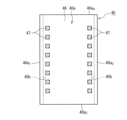
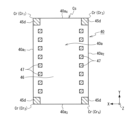
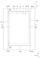
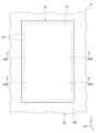
- FIG. FIG. 7 is a plan view schematically showing the configuration of a second semiconductor chip according to modification example 1-1 of the first embodiment of the present technology.
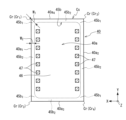
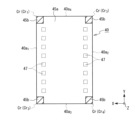
- FIG. 7 is a plan view schematically showing the configuration of a second semiconductor chip according to modification example 1-2 of the first embodiment of the present technology.
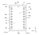
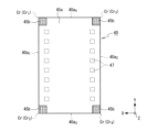
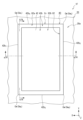
- FIG. 7 is a plan view schematically showing the configuration of a second semiconductor chip according to modification example 1-3 of the first embodiment of the present technology.
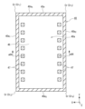
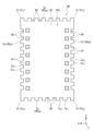
- FIG. 7 is a plan view schematically showing the configuration of a second semiconductor chip according to modification example 1-4 of the first embodiment of the present technology.
- FIG. 7 is a plan view schematically showing the configuration of a second semiconductor chip according to modification example 1-5 of the first embodiment of the present technology.
- FIG. 7 is a plan view schematically showing the configuration of a second semiconductor chip according to modification example 1-6 of the first embodiment of the present technology.
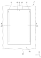
- FIG. 7 is a plan view schematically showing the configuration of a second semiconductor chip according to modification example 1-7 of the first embodiment of the present technology.
- FIG. 7 is a plan view schematically showing the configuration of a second semiconductor chip according to modification example 1-8 of the first embodiment of the present technology.
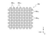
- FIG. 7 is a diagram schematically showing a film state of a warpage suppressing film according to modification example 1-14 of the first embodiment of the present technology.
- FIG. 7 is a plan view schematically showing the configuration of a second semiconductor chip according to modification example 1-15 of the first embodiment of the present technology.
- FIG. 7 is a plan view schematically showing the configuration of a second semiconductor chip according to modification example 1-16 of the first embodiment of the present technology.
- FIG. 7 is a plan view of main parts schematically showing the configuration of a second semiconductor chip according to modification example 1-17 of the first embodiment of the present technology.
- FIG. 7 is a plan view schematically showing the configuration of a second semiconductor chip according to modification example 1-18 of the first embodiment of the present technology.
- FIG. 52 A cross-sectional view schematically showing the configuration of a second semiconductor chip according to modification 1-18 of the first embodiment of the present technology
- (a) is a schematic cross-sectional view of the vertical cross-sectional structure taken along the cutting line a52-a52 in FIG. 52.
- (b) is a vertical cross-sectional view schematically showing the vertical cross-sectional structure along the cutting line b52-b52 in FIG. 52).
- 53 is a vertical cross-sectional view schematically showing a vertical cross-sectional structure at the same position as the b52-b52 cutting line shown in FIG. 52 in a second semiconductor chip according to Modification 1-19 of the first embodiment of the present technology.
- FIG. 3 is a plan view of main parts schematically showing a configuration example of a solid-state imaging device according to a second embodiment of the present technology.
- 56 is a vertical cross-sectional view schematically showing a vertical cross-sectional structure along the a55-a55 cutting line in FIG. 55.
- FIG. 3 is a plan view schematically showing the bonding surface side of the second semiconductor chip.
- FIG. 58 is a vertical cross-sectional view schematically showing the vertical cross-sectional structure along the cutting line a57-a57 in FIG. 57.
- FIG. 58A is an enlarged vertical cross-sectional view of a portion of FIG. 58A.
- FIG. 7 is a plan view schematically showing a planar shape of a warpage suppressing film provided in an inner layer of a multilayer wiring layer of a second semiconductor chip.
- FIG. 7 is a plan view schematically showing a planar pattern of a warpage suppressing film provided on a bonding surface of a multilayer wiring layer in a second semiconductor chip according to modification example 2-1 of the second embodiment of the present technology.
- FIG. 7 is a plan view schematically showing a planar pattern of a warpage suppressing film provided in an inner layer of a multilayer interconnection layer in a second semiconductor chip according to modification example 2-1 of the second embodiment of the present technology.
- FIG. 7 is a plan view schematically showing a planar pattern of a warpage suppressing film provided on a bonding surface of a multilayer interconnection layer in a second semiconductor chip according to modification example 2-2 of the second embodiment of the present technology.
- FIG. 7 is a plan view schematically showing a planar pattern of a warpage suppressing film provided in an inner layer of a multilayer wiring layer in a second semiconductor chip according to modification example 2-2 of the second embodiment of the present technology.
- FIG. 7 is a plan view of main parts schematically showing a configuration example of a solid-state imaging device according to a third embodiment of the present technology.
- 63 is a vertical cross-sectional view schematically showing a vertical cross-sectional structure taken along the line a62-a62 in FIG. 62.
- FIG. 3 is a plan view schematically showing the bonding surface side of the second semiconductor chip.
- 63 is a vertical cross-sectional view schematically showing a vertical cross-sectional structure taken along the line a62-a62 in FIG. 62.
- FIG. 65A is an enlarged vertical cross-sectional view of a portion of FIG. 65A.
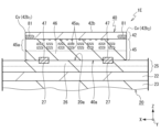
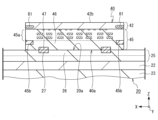
- FIG. 7 is a vertical cross-sectional view schematically showing a vertical cross-sectional structure of a second semiconductor chip according to modification example 3-1 of the third embodiment of the present technology.
- FIG. 7 is a vertical cross-sectional view schematically showing a configuration example of a solid-state imaging device according to a fourth embodiment of the present technology.
- FIG. 3 is a plan view schematically showing the bonding surface side of the second semiconductor chip.
- FIG. 3 is a plan view schematically showing the bonding surface side of the first semiconductor chip.
- FIG. 7 is a plan view of main parts schematically showing a configuration example of a solid-state imaging device according to a fifth embodiment of the present technology.
- 71 is a vertical cross-sectional view schematically showing a vertical cross-sectional structure taken along the cutting line a70-a70 in FIG. 70.
- FIG. 71 is a vertical cross-sectional view schematically showing a vertical cross-sectional structure along the b70-b70 cutting line in FIG. 70.
- FIG. FIG. 12 is a vertical cross-sectional view schematically showing a vertical cross-sectional structure of a solid-state imaging device according to modification example 5-1 of the fifth embodiment of the present technology.
- FIG. 7 is a plan view of main parts schematically showing a configuration example of a solid-state imaging device according to a sixth embodiment of the present technology.
- FIG. 76 is a vertical cross-sectional view schematically showing a vertical cross-sectional structure taken along the cutting line a75-a75 in FIG. 75; 76 is a vertical cross-sectional view schematically showing a vertical cross-sectional structure taken along the b75-b75 cutting line in FIG. 75.
- FIG. FIG. 12 is a plan view of main parts schematically showing a configuration example of a solid-state imaging device according to modification 6-1 of the sixth embodiment of the present technology.
- FIG. 77A is a vertical cross-sectional view schematically showing a vertical cross-sectional structure along the cutting line b77-b77 of FIG. 77A.
- FIG. 12 is a plan view of essential parts schematically showing a configuration example of a solid-state imaging device according to modification 6-2 of the sixth embodiment of the present technology.
- FIG. 78A is a vertical cross-sectional view schematically showing a vertical cross-sectional structure along cutting line a78-a78 in FIG. 78A.
- FIG. 78A is a vertical cross-sectional view schematically showing a vertical cross-sectional structure taken along the cutting line b78-b78 in FIG. 78A.
- FIG. 12 is a plan view of main parts schematically showing a configuration example of a solid-state imaging device according to modification example 6-3 of the sixth embodiment of the present technology.
- 79A is a vertical cross-sectional view schematically showing a vertical cross-sectional structure along the b79-b79 cutting line in FIG. 79A.
- FIG. 11 is a plan view of main parts schematically showing a configuration example of a solid-state imaging device according to modification example 6-4 of the sixth embodiment of the present technology.
- 80A is a vertical cross-sectional view schematically showing a vertical cross-sectional structure along the b80-b80 cutting line in FIG. 80A.
- FIG. 12 is a plan view of main parts schematically showing a configuration example of a solid-state imaging device according to modification example 6-5 of the sixth embodiment of the present technology.
- 81A is a vertical cross-sectional view schematically showing a vertical cross-sectional structure along the a81-a81 cutting line in FIG. 81A.
- FIG. FIG. 7 is a plan view of main parts schematically showing a configuration example of a solid-state imaging device according to a seventh embodiment of the present technology.
- 83 is a vertical cross-sectional view schematically showing a vertical cross-sectional structure along the cutting line a82-a782 in FIG. 82.
- FIG. FIG. 3 is a plan view schematically showing the bonding surface side of the second semiconductor chip.
- FIG. 7 is a plan view schematically showing the bonding surface side of a second semiconductor chip according to Modification Example 7-1 of the seventh embodiment of the present technology.
- FIG. 12 is a vertical cross-sectional view schematically showing a configuration example of a solid-state imaging device according to Modification Example 7-2 of the seventh embodiment of the present technology.
- FIG. 7 is a plan view of main parts schematically showing a configuration example of a solid-state imaging device according to an eighth embodiment of the present technology.
- 87 is a vertical cross-sectional view schematically showing a vertical cross-sectional structure along the cutting line a86a-a86a in FIG. 86.
- FIG. 87 is a vertical cross-sectional view schematically showing a vertical cross-sectional structure along the cutting line a86b-a86b in FIG. 86.
- FIG. FIG. 3 is a plan view schematically showing the bonding surface side of the second semiconductor chip.
- FIG. 12 is a vertical cross-sectional view schematically showing a configuration example of a solid-state imaging device according to modification example 8-1 of the eighth embodiment of the present technology.
- FIG. 12 is a plan view of main parts schematically showing a configuration example of a solid-state imaging device according to a ninth embodiment of the present technology.
- 91 is a vertical cross-sectional view schematically showing a vertical cross-sectional structure along the cutting line a90a-a90a in FIG. 90.
- FIG. 91 is a vertical cross-sectional view schematically showing a vertical cross-sectional structure along the cutting line a90b-a90b in FIG. 90.
- FIG. FIG. 3 is a plan view schematically showing the bonding surface side of the second semiconductor chip.
- FIG. 7 is a plan view of main parts schematically showing a configuration example of a solid-state imaging device according to a tenth embodiment of the present technology.
- 94 is a vertical cross-sectional view schematically showing a vertical cross-sectional structure along the cutting line a93-a93 in FIG. 93.
- FIG. FIG. 3 is a plan view schematically showing the bonding surface side of the second semiconductor chip.
- FIG. 96 is a vertical cross-sectional view schematically showing a vertical cross-sectional structure taken along the b95-b95 cutting line in FIG. 95.
- FIG. FIG. 3 is a plan view schematically showing the bonding surface side of the first semiconductor chip.
- FIG. 9 is a diagram showing types of arrangement patterns of weak bonding regions in modification example 10-1 of the tenth embodiment of the present technology.
- FIG. 11 is a vertical cross-sectional view schematically showing a modification 10-2 of the tenth embodiment of the present technology.
- FIG. 11 is a vertical cross-sectional view schematically showing a modification 10-3 of the tenth embodiment of the present technology.
- FIG. 11 is a vertical cross-sectional view schematically showing a modification 10-4 of the tenth embodiment of the present technology.
- FIG. 10 is a vertical cross-sectional view schematically showing a modification 10-5 of the tenth embodiment of the present technology.
- FIG. 10 is a vertical cross-sectional view schematically showing a modification 10-6 of the tenth embodiment of the present technology.
- FIG. 11 is a vertical cross-sectional view schematically showing a modification 10-7 of the tenth embodiment of the present technology.
- FIG. 11 is a vertical cross-sectional view schematically showing a modification 10-8 of the tenth embodiment of the present technology.
- FIG. 10 is a vertical cross-sectional view schematically showing a modification 10-9 of the tenth embodiment of the present technology.
- FIG. 10 is a vertical cross-sectional view schematically showing a modification 10-10 of the tenth embodiment of the present technology.
- FIG. 10 is a vertical cross-sectional view schematically showing a modification 10-10 of the tenth embodiment of the present technology.
- FIG. 11 is a vertical cross-sectional view schematically showing a modification 10-11 of the tenth embodiment of the present technology.
- FIG. 12 is a vertical cross-sectional view schematically showing a modification 10-12 of the tenth embodiment of the present technology.
- FIG. 12 is a vertical cross-sectional view schematically showing a modification 10-13 of the tenth embodiment of the present technology.
- FIG. 11 is a vertical cross-sectional view schematically showing a modification 10-14 of the tenth embodiment of the present technology.
- FIG. 11 is a vertical cross-sectional view schematically showing a modification 10-15 of the tenth embodiment of the present technology.
- FIG. 12 is a vertical cross-sectional view schematically showing a variation 10-16 of the tenth embodiment of the present technology.
- FIG. 12 is a vertical cross-sectional view schematically showing a modification 10-17 of the tenth embodiment of the present technology.
- FIG. 12 is a diagram showing a schematic configuration of an electronic device according to an eleventh embodiment of the
- the first conductivity type is a p type and the second conductivity type is an n type will be exemplified as the conductivity type of the semiconductor, but if the conductivity types are selected in the opposite relationship,
- the first conductivity type may be n type and the second conductivity type may be p type.
- a first direction and a second direction that are orthogonal to each other in the same plane are respectively referred to as an X direction and a Y direction
- the first direction and A third direction perpendicular to each of the second directions is defined as a Z direction.
- the thickness direction of the first semiconductor chip 20 and second semiconductor chip 40 which will be described later, will be described as the Z direction.
- CMOS Complementary Metal Oxide Semiconductor
- the solid-state imaging device 1A includes a first semiconductor chip 20 having a bonding surface 20a as an example of a base member, and a rectangular bonding surface 40a.
- a second semiconductor chip 40 The bonding surface 20a of the first semiconductor chip 20 and the bonding surface 40a of the second semiconductor chip 40 are bonded together by direct bonding.
- the first embodiment includes two second semiconductor chips 40 and 40 whose planar size is smaller than the planar size of the first semiconductor chip 20.
- Each of the two second semiconductor chips 40 is spaced apart from each other within the two-dimensional plane of the first semiconductor chip 20.
- Each of the first semiconductor chip 20 and the second semiconductor chip 40 has a rectangular two-dimensional planar shape when viewed from above.
- As the direct bonding of the second semiconductor chip 40 for example, surface activated bonding can be used.
- the direct bonding of the second semiconductor chip 40 is performed before the first semiconductor chip 20 is formed by cutting a chip forming region 65 (see FIG. 24) of the wafer stack 60 (described later) into small pieces. (see).
- the solid-state imaging device 1A according to the first embodiment of the present technology further includes a sealing body 51 provided on the bonding surface 20a side of the first semiconductor chip 20 to cover the second semiconductor chip 40.
- a sealing body 51 for example, an epoxy-based thermosetting insulating resin or a polyimide-based thermoplastic insulating resin can be used.
- the sealing body 51 has a rectangular shape in plan view, and in the first embodiment, it has a rectangular shape similar to the first semiconductor chip 20, for example.
- the first semiconductor chip 20 corresponds to a specific example of the "base member” of the present technology.
- the second semiconductor chip 40 corresponds to a specific example of the "semiconductor chip” of the present technology.
- the bonding surface 20a of the first semiconductor chip 20 corresponds to a specific example of the "first bonding surface” of the present technology
- the bonding surface 40a of the second semiconductor chip 40 corresponds to an example of the "second bonding surface” of the present technology. This corresponds to a specific example.
- a plan view refers to a case viewed from a direction along the thickness direction (Z direction) of the semiconductor chips 20, 40.
- a cross-sectional view is a cross section along the thickness direction (Z direction) of the semiconductor chips 20, 40 viewed from a direction (X direction or Y direction) orthogonal to the thickness direction (Z direction) of the semiconductor chips 20, 40. refers to the case
- the solid-state imaging device 1A (101) takes in image light (incident light 106) from a subject through an optical lens 102, and forms an image on an imaging surface.
- the amount of incident light 106 is converted into an electrical signal for each pixel and output as a pixel signal (image signal).
- the first semiconductor chip 20 includes a rectangular pixel array section 2A provided at the center, and a rectangular pixel array section 2A provided at the center in a two-dimensional plane including the X direction and Y direction that are orthogonal to each other.
- a peripheral portion 2B is provided outside to surround the pixel array portion 2A.
- the pixel array section 2A is a light receiving surface that receives light collected by an optical lens (optical system) 102 shown in FIG. 39, for example.
- a plurality of pixels 3 are arranged in a matrix on a two-dimensional plane including the X direction and the Y direction.
- the pixels 3 are repeatedly arranged in the X direction and the Y direction, which are orthogonal to each other within a two-dimensional plane.
- the vertical drive circuit 4 is composed of, for example, a shift register.
- the vertical drive circuit 4 sequentially selects desired pixel drive lines 10, supplies pulses for driving the pixels 3 to the selected pixel drive lines 10, and drives each pixel 3 row by row. That is, the vertical drive circuit 4 sequentially selectively scans each pixel 3 of the pixel array section 2A in the vertical direction row by row, and generates a signal charge generated by the photoelectric conversion section (photoelectric conversion element) of each pixel 3 according to the amount of light received.
- a pixel signal from the pixel 3 based on the above is supplied to the column signal processing circuit 5 through the vertical signal line 11.
- the column signal processing circuit 5 is arranged, for example, for each column of pixels 3, and performs signal processing such as noise removal on the signals output from one row of pixels 3 for each pixel column.
- the column signal processing circuit 5 performs signal processing such as CDS (Correlated Double Sampling) and AD (Analog Digital) conversion to remove fixed pattern noise specific to pixels.
- the horizontal drive circuit 6 is composed of, for example, a shift register.
- the horizontal drive circuit 6 sequentially outputs horizontal scanning pulses to the column signal processing circuits 5 to select each of the column signal processing circuits 5 in turn, and selects pixels on which signal processing has been performed from each of the column signal processing circuits 5.
- the signal is output to the horizontal signal line 12.
- the output circuit 7 performs signal processing on the pixel signals sequentially supplied from each column signal processing circuit 5 through the horizontal signal line 12 and outputs the signal.
- signal processing for example, buffering, black level adjustment, column variation correction, various digital signal processing, etc. can be used.
- the control circuit 8 generates clock signals and control signals that serve as operating standards for the vertical drive circuit 4, column signal processing circuit 5, horizontal drive circuit 6, etc., based on the vertical synchronization signal, horizontal synchronization signal, and master clock signal. generate. Then, the control circuit 8 outputs the generated clock signal and control signal to the vertical drive circuit 4, column signal processing circuit 5, horizontal drive circuit 6, and the like.
- each pixel 3 of the plurality of pixels 3 includes a photoelectric conversion region 35 and a pixel circuit (readout circuit) 15.
- the photoelectric conversion region 35 includes a photoelectric conversion section 16, a transfer transistor TR, and a charge retention region (floating diffusion) FD.
- the pixel circuit 15 is electrically connected to the charge retention region FD of the photoelectric conversion region 35.
- one pixel circuit 15 is allocated to one pixel 3 as an example, but the circuit configuration is not limited to this, and one pixel circuit 15 is shared by a plurality of pixels 3.
- the photoelectric conversion unit 16 shown in FIG. 2 is composed of, for example, a pn junction type photodiode (PD), and generates signal charges according to the amount of received light.
- the photoelectric conversion unit 16 has a cathode side electrically connected to the source region of the transfer transistor TR, and an anode side electrically connected to a reference potential line (for example, ground).
- the charge holding region FD shown in FIG. 2 temporarily holds (accumulates) the signal charges transferred from the photoelectric conversion section 16 via the transfer transistor TR.
- a photoelectric conversion region 35 including the photoelectric conversion section 16, transfer transistor TR, and charge retention region FD is mounted on a semiconductor layer 32 (see FIG. 5), which will be described later. Further, although not limited thereto, for example, pixel transistors (AMP, SEL, RST, FDG) included in the pixel circuit 15 are also mounted on the semiconductor layer 32.
- pixel transistors AMP, SEL, RST, FDG
- the pixel circuit 15 shown in FIG. 2 reads out the signal charge held in the charge holding region FD, converts the read out signal charge into a pixel signal, and outputs the pixel signal.
- the pixel circuit 15 converts the signal charge photoelectrically converted by the photoelectric conversion unit 16 (photoelectric conversion element PD) into a pixel signal based on this signal charge, and outputs the pixel signal.
- the pixel circuit 15 includes, for example, an amplification transistor AMP, a selection transistor SEL, a reset transistor RST, and a switching transistor FDG as pixel transistors.
- Each of these pixel transistors (AMP, SEL, RST, FDG) and the above-mentioned transfer transistor TR are configured with, for example, a MOSFET as a field effect transistor. Moreover, MISFETs may be used as these transistors.
- the selection transistor SEL, reset transistor RST, and switching transistor FDG each function as a switching element
- the amplification transistor AMP functions as an amplification element
- the amplification transistor AMP has a source region electrically connected to the drain region of the selection transistor SEL, and a drain region electrically connected to the power supply line Vdd and the drain region of the reset transistor RST.
- the gate electrode of the amplification transistor AMP is electrically connected to the charge holding region FD and the source region of the switching transistor FDG.
- the selection transistor SEL has a source region electrically connected to the vertical signal line 11 (VSL), and a drain region electrically connected to the source region of the amplification transistor AMP.
- the gate electrode of the selection transistor SEL is electrically connected to the selection transistor drive line of the pixel drive lines 10 (see FIG. 1).
- the reset transistor RST has a source region electrically connected to the drain region of the switching transistor FDG, and a drain region electrically connected to the power supply line Vdd and the drain region of the amplification transistor AMP.
- the gate electrode of the reset transistor RST is electrically connected to a reset transistor drive line among the pixel drive lines 10 (see FIG. 1).
- the switching transistor FDG has a source region electrically connected to the charge holding region FD and the gate electrode of the amplification transistor AMP, and a drain region electrically connected to the power supply line Vdd and the drain region of the amplification transistor AMP.
- the gate electrode of the switching transistor FDG is electrically connected to a switching transistor drive line among the pixel drive lines 10 (see FIG. 1).
- the selection transistor SEL and the switching transistor FDG may be omitted as necessary.
- the source region of the amplification transistor AMP is electrically connected to the vertical signal line 11 (VSL).
- the switching transistor FDG is omitted, the source region of the reset transistor RST is electrically connected to the gate electrode of the amplification transistor AMP and the charge holding region FD.
- the transfer transistor TR shown in FIG. 2 transfers the signal charge generated in the photoelectric conversion section 16 to the charge holding region FD when the transfer transistor TR is turned on.
- the reset transistor RST shown in FIG. 2 resets the potential (signal charge) of the charge holding region FD to the potential of the power supply line Vdd when the reset transistor RST is turned on.
- the selection transistor SEL controls the output timing of the pixel signal from the pixel circuit 15.
- the amplification transistor AMP generates, as a pixel signal, a voltage signal corresponding to the level of the signal charge held in the charge holding region FD.
- the amplification transistor AMP constitutes a source follower type amplifier, and outputs a pixel signal of a voltage corresponding to the level of the signal charge generated by the photoelectric conversion section 16.
- the selection transistor SEL is turned on, the amplification transistor AMP amplifies the potential of the charge holding region FD and outputs a voltage corresponding to the potential to the column signal processing circuit 5 via the vertical signal line 11 (VSL). do.
- the switching transistor FDG shown in FIG. 2 controls charge retention by the charge retention region FD, and also adjusts the voltage multiplication factor according to the potential amplified by the amplification transistor AMP.
- signal charges generated in the photoelectric conversion section 16 of the pixel 3 are held via the transfer transistor TR of the pixel 3. It is held (stored) in the area FD. Then, the signal charge held in the charge holding region FD is read out by the pixel circuit 15 and applied to the gate electrode of the amplification transistor AMP of the pixel circuit 15. A horizontal line selection control signal is applied to the gate electrode of the selection transistor SEL of the pixel circuit 15 from the vertical shift register.
- the selection transistor SEL becomes conductive, and a current corresponding to the potential of the charge holding region FD amplified by the amplification transistor AMP flows to the vertical signal line 11. Furthermore, by setting the reset control signal applied to the gate electrode of the reset transistor RST of the pixel circuit 15 to a high (H) level, the reset transistor RST becomes conductive and resets the signal charge accumulated in the charge holding region FD. .
- the second semiconductor chip 40 has an internal circuit 17 electrically connected to the logic circuit 13 of the first semiconductor chip 20.
- Examples of the internal circuit 17 include storage circuits such as DRAM and flash memory, and control circuits.
- FIGS. 8 and 9 are upside down compared to FIGS. 4 and 5.
- FIGS. 12A, 12B, and 13 are upside down compared to FIGS. 8 and 9.
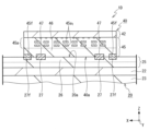
- the solid-state imaging device 1A has a chip stacked structure in which a first semiconductor chip 20 and a second semiconductor chip 40 are stacked with their bonding surfaces facing each other. . That is, the solid-state imaging device 1A includes a chip stack including a first semiconductor chip 20 and a second semiconductor chip 40.
- the first semiconductor chip 20 includes a first substrate section 21 and a second substrate section 31, each of which is stacked facing each other in the thickness direction (Z direction). .
- the first substrate section 21 is provided with the above-mentioned logic circuit 13 and the like.
- the second substrate section 31 is provided with the above-described pixel array section 2A, peripheral section 2B, pixel transistors included in the pixel circuit 15, bonding pads 14, and the like.
- the first substrate section 21 and the second substrate section 31 can also each be expressed as a semiconductor chip.
- the second substrate portion 31 has a first surface (element forming surface, main surface) and a second surface (light incident surface) located on opposite sides in the thickness direction (Z).
- the multilayer wiring layer 33 is provided on the first surface side of the semiconductor layer 32.
- the second substrate portion 31 is provided in order from the semiconductor layer 32 side on the light incident surface side (second surface side) opposite to the multilayer wiring layer 33 side (first surface side) of the semiconductor layer 32.
- An optical filter layer 36 and a microlens 37 are provided.
- the first semiconductor chip 20 has a rectangular planar shape when viewed from above, and in the first embodiment, it has a rectangular shape, for example.
- the semiconductor layer 32 extends two-dimensionally over the pixel array section 2A and the peripheral section 2B, and overlaps with the pixel array section 2A and the peripheral section 2B in plan view.
- a Si substrate, a SiGe substrate, an InGaAs substrate, etc. can be used as the semiconductor layer 32.
- the semiconductor layer 32 is formed using a semiconductor substrate made of, for example, silicon (Si) as the semiconductor material, single crystal as the crystallinity, and p-type as the conductivity type, although the semiconductor layer 32 is not limited thereto. There is.
- the above-described photoelectric conversion region 35 is provided in the semiconductor layer 32.
- the photoelectric conversion regions 35 are repeatedly arranged for each pixel 3 in the X direction and the Y direction, which are orthogonal to each other, for example, in a two-dimensional plane.
- a transfer transistor TR is provided that transfers signal charges photoelectrically converted by the photoelectric conversion section 16 to a charge holding region.
- the photoelectric conversion section 16, the charge retention region FD, and the transfer transistor TR are provided in the semiconductor layer 32 for each pixel 3 (photoelectric conversion region 35).
- the multilayer wiring layer 33 has a laminated structure in which insulating layers and wiring layers are alternately stacked in multiple stages.
- the multilayer wiring layer 33 includes wiring provided in each wiring layer and a bonding metal pad 34.
- a material for the insulating layer for example, silicon oxide (SiO 2 ) can be used.
- As the material for the wiring layer and the bonding metal pad 34 for example, metals such as aluminum (Al) and copper (Cu), or alloys mainly composed of Al and Cu can be used.
- the wiring provided in the uppermost wiring layer of the multilayer wiring layer 33 is covered with the uppermost insulating layer.
- the bonding metal pad 34 is provided on the surface layer portion of the multilayer wiring layer 33 on the side opposite to the semiconductor layer 32 side, and is provided in the insulating layer with the surface exposed from the uppermost insulating layer.
- the bonding metal pad 34 is electrically connected to the wiring layer below the bonding metal pad 34.
- the lower layer wiring is electrically connected to the charge retention region FD and the transfer transistor TR.
- the optical filter layer 36 color-separates the incident light that has entered from the light incident surface side (back surface side) of the first semiconductor chip 20 .
- the optical filter layer 36 includes, for example, a first color filter of red (R), a second color filter of green (G), and a third color filter of blue (B).
- the microlens 37 is provided for each photoelectric conversion region 35 on the side of the optical filter layer 36 opposite to the semiconductor layer 32 side (light incident surface side).
- the microlens 37 condenses the irradiated light and allows the condensed light to enter the photoelectric conversion unit 16 efficiently.
- the first substrate section 21 has a first surface (element forming surface) and a second surface (back surface) located on opposite sides in the thickness direction (Z direction). It includes a semiconductor layer 22, a multilayer wiring layer 23 provided on the first surface side of the semiconductor layer 22, and a multilayer wiring layer 25 provided on the second surface side of the semiconductor layer 22.
- the semiconductor layer 22 extends two-dimensionally over the pixel array section 2A and the peripheral section 2B, and overlaps the pixel array section 2A and the peripheral section 2B in plan view.
- a Si substrate, a SiGe substrate, an InGaAs substrate, etc. can be used as the semiconductor layer 22 .
- the semiconductor layer 22 is formed using a semiconductor substrate made of, for example, silicon (Si) as the semiconductor material, single crystal as the crystallinity, and p-type as the conductivity type, although the semiconductor layer 22 is not limited thereto. There is.
- MOSFET Metal Oxide Semiconductor Field Effect Transistor
- the multilayer wiring layer 23 has a laminated structure in which insulating layers and wiring layers are alternately stacked in multiple stages.
- the multilayer wiring layer 23 includes wiring provided in each wiring layer and a bonding metal pad 24.
- a material for the insulating layer for example, silicon oxide (SiO 2 ) can be used.
- metals such as aluminum (Al) and copper (Cu), or alloys mainly composed of Al and Cu can be used.
- the wiring provided in the uppermost wiring layer of the multilayer wiring layer 23 is covered with the uppermost insulating layer.
- the bonding metal pad 24 is provided on the surface layer portion of the multilayer wiring layer 23 on the side opposite to the semiconductor layer 22 side, and the surface thereof is exposed from the uppermost insulating layer.
- the bonding metal pad 24 is electrically connected to the wiring layer below the bonding metal pad 24.
- the multilayer wiring layer 25 has a laminated structure in which insulating layers and wiring layers are alternately stacked in multiple stages.
- the multilayer wiring layer 25 includes wiring provided in each wiring layer and a bonding metal pad 27.
- a material for the insulating layer for example, silicon oxide (SiO 2 ) can be used.
- metals such as aluminum (Al) and copper (Cu), or alloys mainly composed of Al and Cu can be used.
- the wiring provided in the uppermost wiring layer of the multilayer wiring layer 25 is covered with the uppermost insulating layer 26 (see FIGS. 8 and 9) of the multilayer wiring layer 25.
- the bonding metal pad 27 is provided on the surface layer portion of the multilayer wiring layer 25 on the side opposite to the semiconductor layer 22 side, and is provided in the insulating layer 26 with the surface exposed from the uppermost insulating layer 26. .
- the bonding metal pad 27 is electrically connected to the wiring layer below the bonding metal pad 27 .
- the wiring of the multilayer wiring layer 25 is electrically connected to the wiring of the multilayer wiring layer 23 via the contact electrode 28 shown in FIGS. 4 and 5.
- the contact electrode 28 penetrates the semiconductor layer 22 in the thickness direction of the semiconductor layer 22 and extends over the multilayer wiring layer 23, the semiconductor layer 22, and the multilayer wiring layer 25.
- a high melting point metal such as titanium (Ti) or tungsten (W) can be used.
- the bonding pad 14 is provided on the semiconductor layer 32 side of the multilayer wiring layer 33. Specifically, the bonding pad 14 is provided, for example, in the first wiring layer of the multilayer wiring layer 33.
- the first semiconductor chip 20 is provided with a bonding opening 38 that exposes the surface of the bonding pad 14.
- the bonding opening 38 penetrates the semiconductor layer 32 in the thickness direction (Z direction) of the semiconductor layer 32 and extends across the semiconductor layer 32 and the multilayer wiring layer 33 .
- a connecting member such as a bonding wire or a bump electrode is electrically and mechanically connected to the bonding pad 14 through this bonding opening 38 .
- the first substrate portion 21 is provided with a bonding metal pad 24 on a surface layer portion of the multilayer wiring layer 23 on the side opposite to the semiconductor layer 22 side.
- the bonding metal pad 24 is provided in the uppermost insulating layer of the multilayer wiring layer 23 with its bonding surface exposed.
- the second substrate portion 31 has the bonding metal pad 34 provided on the surface layer portion of the multilayer wiring layer 33 on the side opposite to the semiconductor layer 32 side.
- the bonding metal pad 34 is provided in the uppermost insulating layer of the multilayer wiring layer 33 with its bonding surface exposed.
- the bonding metal pad 24 of the first substrate section 21 and the bonding metal pad 34 of the second substrate section 31 are electrically and mechanically connected by respective metal-to-metal bonding with their bonding surfaces facing each other. .
- the metal-to-metal bond between the bonding metal pad 24 and the bonding metal pad 34 electrically connects the wiring in the multilayer wiring layer 23 of the first substrate section 21 and the wiring in the multilayer wiring layer 33 of the second substrate section 31. Conduct.
- the bonding surfaces of the bonding metal pad 24 of the first substrate portion 21 and the bonding metal pad 34 of the second substrate portion 31 are directly bonded. Further, the uppermost insulating layer of the multilayer wiring layer of the first substrate section 21 and the uppermost insulating layer of the multilayer wiring layer of the second substrate section 31 are joined at their bonding surfaces by direct bonding. For example, surface activated bonding can be used as direct bonding.
- the bonding surface 20a of the first semiconductor chip 20 is provided on the insulating layer 26 side of the multilayer wiring layer 25.
- the bonding surface 20a of the first semiconductor chip 20 includes an insulating layer 26 located at the top layer of the multilayer wiring layer 25 of the first semiconductor chip 20, Includes interspersed bonding metal pads 27.
- the bonding metal pads 27 are scattered in the chip mounting area Cm of the bonding surface 20a.
- the second semiconductor chip 40 is mounted in this chip mounting area Cm, and the joint surface 40a of the second semiconductor chip 40 is directly joined.
- the insulating layer 26 of the multilayer wiring layer 25 corresponds to a specific example of the "first insulating layer” of the present technology
- the bonding metal pad 27 of the multilayer wiring layer 25 corresponds to a "first insulating layer” of the present technology. This corresponds to a specific example of "first bonding metal pad”.
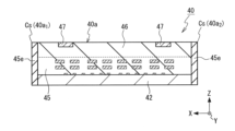
- each of the two second semiconductor chips 40 has a first surface (element formation surface, main surface) and a second surface located on opposite sides in the thickness direction (Z). It includes a semiconductor layer 42 having a front surface (back surface), and a multilayer wiring layer 45 provided on the first surface side of the semiconductor layer 42. That is, each of the two second semiconductor chips 40 includes a multilayer wiring layer 45 including a second bonding surface 40a, and a semiconductor layer 42 provided on the side of the multilayer wiring layer 45 opposite to the second bonding surface 40a. , is equipped with.
- the semiconductor layer 42 As the semiconductor layer 42, a Si substrate, a SiGe substrate, an InGaAs substrate, etc. can be used.
- the semiconductor layer 42 is formed using a semiconductor substrate made of, for example, silicon (Si) as the semiconductor material, single crystal as the crystallinity, and p-type as the conductivity type, although the semiconductor layer 42 is not limited thereto.
- Si silicon
- a MOSFET Metal Oxide Semiconductor Field Effect Transistor
- the multilayer wiring layer 45 includes a multilayer stacked part 45a in which insulating layers and wiring layers are alternately stacked in multiple stages, and a multilayer stacked part 45a on the side opposite to the semiconductor layer 42 side.
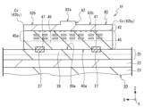
- a warp suppressing film 45b provided as a warp suppressing portion is included.
- the multilayer wiring layer 45 includes an insulating layer 46 provided covering the warpage suppressing film 45b on the opposite side of the multilayer stacked portion 45a from the semiconductor layer 42 side, and an insulating layer 46 provided on the opposite side of the multilayer stacked portion 45a from the side of the multilayer stacked portion 45a.
- the insulating layer 46 is the uppermost insulating layer of the multilayer wiring layer 45, and the surface of the insulating layer 46 is the bonding surface 40a of the second semiconductor chip 40. That is, the bonding surface 40a of the second semiconductor chip 40 includes the uppermost insulating layer 46 of the multilayer wiring layer 45 and bonding metal pads 47 scattered on the insulating layer 46.
- the bonding metal pad 47 is provided in the insulating layer 46 of the multilayer wiring layer 45 with its bonding surface exposed.
- the bonding surface 40a is generally flat with a step difference between the bonding metal pad 47 and the insulating layer 46 as small as possible.
- a silicon oxide (SiO 2 ) film can be used as the material for the insulating layer of the multi-layer stack 45a and the uppermost insulating layer 46.
- a metal such as aluminum (Al) or copper (Cu), or an alloy mainly composed of Al or Cu can be used.
- the bonding metal pad 47 is electrically connected to the wiring layer below the bonding metal pad 47.
- the lower layer wiring is electrically connected to the transistor provided on the first surface side of the semiconductor layer 42.
- the second semiconductor chip 40 has a rectangular planar shape when viewed from above, and in the first embodiment, it has a rectangular shape, for example.
- the bonding surface 40a of the second semiconductor chip 40 also has a rectangular shape, which is an example of a rectangular shape.
- FIG. 12A, FIG. 12B, and FIG. 13 show the state before the second semiconductor chip 40 is directly bonded to the wafer stack described later. Furthermore, since the first semiconductor chip 20 is formed by cutting a chip forming area 65 of a wafer stack 60, which will be described later, into small pieces, for convenience, "wafer stack" will be replaced with "second semiconductor chip” in the description. Sometimes.
- the bonding surface 40a of the second semiconductor chip 40 is provided on the insulating layer 46 side of the multilayer wiring layer 45.
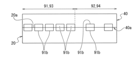
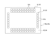
- the joint surface 40a has two sides 40a 1 and 40a 2 located on opposite sides in the X direction, and two sides 40a 3 and 40a 4 located on opposite sides in the Y direction. and has.
- the two sides 40a 1 and 40a 2 extend in the Y direction.
- the two sides 40a 3 and 40a 4 extend in the X direction.
- the two sides 40a 1 and 40a 2 are sometimes referred to as long sides. Further, the two sides 40a 3 and 40a 4 may also be referred to as short sides.
- the second semiconductor chip 40 has a peripheral edge Cs including four sides 40a 1 , 40a 2 , 40a 3 and 40a 4 of the bonding surface 40a.
- the peripheral edge portion Cs has a curved shape that extends over the bonding surface 40a and the side surface of the second semiconductor chip 40.
- the curved peripheral edge portion Cs is formed by performing ring CMP on the bonding surface 40a of the second semiconductor chip 40 in the manufacturing process of the second semiconductor chip 40, which will be described later.
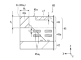
- the warp suppressing film 45b of the multilayer wiring layer 45 extends along at least one side of the bonding surface 40a of the second semiconductor chip 40.
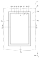
- the warp suppressing film 45b is provided on the four sides (40a 1 , 40a 2 , 40a 3 , 40a 4 ) of the bonding surface 40a of the second semiconductor chip 40. , and has an annular plane pattern extending continuously along these four sides (40a 1 , 40a 2 , 40a 3 , 40a 4 ).
- the warpage suppressing film 45b overlaps the sides (40a 1 , 40a 2 , 40a 3 , 40a 4 ) of the bonding surface 40a of the second semiconductor chip 40 in plan view, and is exposed from the side surface of the second semiconductor chip 40. There is.
- the warpage suppressing film 45b is arranged on the outer peripheral portion (peripheral edge Cs side) of the second semiconductor chip 40 to control local film stress of the second semiconductor chip 40 and prevent warping of the second semiconductor chip 40. suppress.
- the manufacturing process of the solid-state imaging device 1A according to the first embodiment involves forming the chip forming area 65 of the wafer stack 60.
- the method includes a thinning step of reducing the thickness of the second semiconductor chip 40 in the Z direction after directly joining the joining surface 40a of the second semiconductor chip 40 to the joining surface 20a (the joining surface 20a of the first semiconductor chip). It is.
- the thickness of the semiconductor layer 42 of the second semiconductor chip 40 in the Z direction is reduced, so that the rigidity of the second semiconductor chip 40 is reduced.
- the outer peripheral part of the second semiconductor chip 40 (peripheral part Cs side of the second semiconductor chip 40) is reduced to the bonding surface 20a of the chip forming area 65 of the wafer stack 60 (first semiconductor
- the second semiconductor chip 40 may be warped away from the bonding surface 20a of the chip, that is, the second semiconductor chip 40 may be warped so that the bonding surface 40a of the second semiconductor chip 40 is a convex surface.
- the warpage suppressing film 45b suppresses such warping of the second semiconductor chip 40.
- a material having a linear expansion coefficient different from that of the surrounding multi-layer stacked portion 45a and the insulating layer 46 is used.
- the rigidity is increased. As a result, it becomes possible to suppress warping of the peripheral portion of the semiconductor chip 40 due to the difference in linear expansion coefficient.
- the warp suppressing film 45b is arranged between the multi-layer stacked portion 45a and the insulating layer 46.
- the thickness t 1 of the warp suppressing film 45b is thicker than the thickness t 2 of the wiring 45a 1 of the multilayer wiring layer 45 in order to enable control of local film stress of the second semiconductor chip 40 ( t 1 > t 2 ).
- the thickness t 1 of the warp suppressing film 45b is preferably thicker than the thickness t 3 of the bonding metal pad 47 of the multilayer wiring layer 45.
- the warp suppressing film 45b is made of a material different from that of the insulating layer of the multi-layer stacked portion 45a of the multilayer interconnection layer 45 and the uppermost insulating layer 46 of the multilayer interconnection layer 45.
- the warp suppressing film 45b may be an insulating film such as a SiO film, a SiCO film, a SiO film, a SiCN film, or a silicon nitride (SiN) film, an aluminum (Al) film, a copper (Cu) film, or a tungsten (W) film.
- the insulating layer 46 is a silicon oxide layer, a silicon nitride film, an aluminum nitride film, or a hafnium nitride film is preferable because a better processing selectivity with respect to the silicon oxide layer can be obtained.
- the warpage suppressing film 45b is made of, for example, a silicon nitride film.
- the bonding metal pads 27 of the first semiconductor chip 20 and the bonding metal pads 47 of the second semiconductor chip 40 are bonded together by direct bonding, with their bonding surfaces facing each other. has been done.
- the insulating layer 26 of the first semiconductor chip 20 and the insulating layer 46 of the second semiconductor chip 40 are directly bonded to each other so as to face each other. That is, the bonding surface 20a including the insulating layer 26 and bonding metal pad 27 of the first semiconductor chip 20 and the bonding surface 40a including the insulating layer 46 and bonding metal pad 47 of the second semiconductor chip 40 are bonded by direct bonding.
- direct bonding There is.
- surface activated bonding can be used as direct bonding.
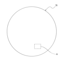
- FIG. 14 is a schematic plan view of a semiconductor wafer 70 for explaining a method of manufacturing the second semiconductor chip 40 included in the solid-state imaging device 1A according to the first embodiment of the present technology.
- FIG. 15 is an enlarged view of area A in FIG. 14 showing the configuration of the chip forming area 75.
- 16 is a vertical cross-sectional view schematically showing the vertical cross-sectional structure along the cutting line a15-a15 in FIG.
- FIG. 2 is a plan view schematically showing the state in which FIG.
- FIG. 18 is a vertical cross-sectional view schematically showing the vertical cross-sectional structure along the a17-a17 cutting line in FIG.
- FIG. 19 is a vertical cross-sectional view schematically showing a state in which a ring CMP step is performed in the method for manufacturing the second semiconductor chip 40.
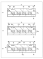
- FIGS. 20 and 21 are process cross-sectional views schematically showing the formation of the multilayer wiring layer 45 including the warp suppressing film 45b and the bonding surface 40a in the method of manufacturing the second semiconductor chip 40.
- the semiconductor wafer 70 shown in FIG. 14 has already undergone a pre-process of forming transistors, multilayer wiring layers 45, etc. on the semiconductor layer 42 (see FIG. 16), and the chip forming area 75 shown in FIG. A semiconductor layer 42, a multilayer wiring layer 45, a bonding surface 40a, etc. shown in FIG.
- the bonding surface 40a includes the insulating layer 46 of the multilayer wiring layer 45 and the bonding metal pad 47.
- the semiconductor wafer 70 that has been subjected to the pre-processing is diced along the scribe lines 76, and as shown in FIGS. 17 and 18, the plurality of chip forming regions 65 of the semiconductor wafer 70 are individually diced to form the second semiconductor chip 40. form. Dicing of the semiconductor wafer 70 is performed with the semiconductor wafer 70 adhesively fixed to a dicing sheet (dicing tape) 79.
- the second semiconductor chip 40 includes a bonding surface 40a and a warpage suppressing film 45b, and the bonding surface 40a includes an insulating layer 46 and a bonding metal pad 47.
- FIG. 19 shows the peripheral edge Cs of the two sides 40a 1 and 40a 2 of the bonding surface 40a in a cross section of the second semiconductor chip 40 along the X direction.
- the second semiconductor chip 40 is transported to a chip bonding step in the manufacturing process of the solid-state imaging device 1A, which will be described later. .
- the multilayer wiring layer 45 is formed in a wafer state before the second semiconductor chips 40 are formed by individually cutting the plurality of chip forming regions 65 of the semiconductor wafer 70 into pieces.
- a multi-layered layered portion 45a in which a plurality of insulating layers and wiring layers are alternately stacked is formed on the element forming surface side of the semiconductor layer 42.
- a warp suppressing film 45b is formed on the entire surface of the multi-layered stacked portion 45a on the side opposite to the semiconductor layer 42 side.
- an insulating film such as a silicon nitride (SiN) film, a metal film such as an aluminum (Al) film, a copper (Cu) film, or an alloy film thereof, or a resin film can be used.
- a silicon nitride film is formed as the warpage suppressing film 45b by, for example, the CVD method.
- the warp suppressing film 45b is patterned into a predetermined shape, and as shown in FIG. 20(c), the warp suppressing film 45b having a predetermined shape is formed on the multi-layer stacked portion 45a. Patterning of the warpage suppressing film 45b is performed using well-known photolithography technology and anisotropic dry etching technology. Although not shown in detail, the warpage suppressing film 45b is formed in a shape extending along at least one of the four sides of the chip forming region 75 in plan view. In the first embodiment, for example, although not limited thereto, the warpage suppressing film 45b is formed in an annular pattern that extends continuously along the four sides of the chip forming region 75 in plan view.
- an insulating layer 46 covering the warp suppressing film 45b is formed on the entire surface of the multi-layer stacked portion 45a on the side opposite to the semiconductor layer 42 side.
- the insulating layer 46 can be formed, for example, by depositing a silicon oxide film using a CVD method.
- a recess 46a is formed in the surface layer portion of the insulating layer 46 on the side opposite to the multi-layer stacked portion 45a side.
- This recess 46a is formed using well-known photolithography technology and anisotropic dry etching technology.
- a metal film 47A is formed on the entire surface of the insulating layer 46 on the side opposite to the multi-layered layered portion 45a so as to fill the recess 46a.
- a metal film such as aluminum (Al) or copper (Cu), or an alloy film such as an alloy mainly composed of Al or Cu can be used.
- These metal films and alloy films can be formed by, for example, a sputtering method.
- the metal film 47A on the insulating layer 46 is selectively removed so that the metal film 47A remains inside the recess 46a of the insulating layer 46, and as shown in FIG. A bonding metal pad 47 is formed in the recess 46a.
- Selective removal of the metal film 47A is performed by, for example, a CMP method.
- a bonding surface 40a including the insulating layer 46 and the bonding metal pads 47 scattered on the insulating layer 46 is formed in the chip forming region 75. Further, by this step, a multilayer interconnection layer 45 including a multilayer stacked portion 45a, a warpage suppressing film 45b, and a bonding surface 40a is formed.
- FIG. 22 is a diagram showing the planar configuration of the wafer stack.
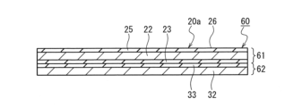
- FIG. 23 is a vertical cross-sectional view schematically showing the vertical cross-sectional structure of the wafer stack 60.
- FIG. 24 is an enlarged view of region B in FIG. 23 schematically showing the configuration of the chip forming region 65. As shown in FIG.
- FIG. 25, FIG. 27, FIG. 31, and FIG. 34 are plan views schematically showing the steps of the manufacturing method of the solid-state imaging device 1A
- FIG. 26 is a vertical cross-sectional view schematically showing the vertical cross-sectional structure along the a25-a25 cutting line in FIG.
- FIG. 28 is a vertical cross-sectional view schematically showing the vertical cross-sectional structure along the a27-a27 cutting line in FIG.
- FIG. 29 is an enlarged vertical cross-sectional view of a part of FIG. 28,
- FIG. 30 is a vertical cross-sectional view schematically showing a step subsequent to FIG. 27,
- FIG. 33 is a vertical cross-sectional view schematically showing a process subsequent to FIG. 31;
- FIG. 34 is a plan view schematically showing a step subsequent to FIG. 33.
- the first semiconductor chip 20 included in the solid-state imaging device 1A is manufactured in the chip forming area 65 of the wafer stack 60 shown in FIG.
- the chip forming regions 65 are divided by scribe lines (dicing lines) 66 extending along each of the X direction and the Y direction, and are arranged in a plurality of rows and columns.
- FIG. 24 illustrates nine chip forming regions 65 arranged three in each of the X direction and the Y direction.
- the first semiconductor chip 20 is formed by individually cutting the plurality of chip forming regions 65 into pieces along the scribe lines 66.
- the chip formation region 65 is divided into pieces after the manufacturing process described below is performed.
- the wafer stack 60 includes two semiconductor wafers 61 and 62 stacked on each other.
- the semiconductor wafer 61 includes a semiconductor layer 22, a multilayer wiring layer 23 laminated on the element forming surface side of the semiconductor layer 22, and a multilayer wiring layer laminated on the opposite side of the semiconductor layer 22 from the multilayer wiring layer 23 side. 25.
- the semiconductor wafer 62 includes a semiconductor layer 32 and a multilayer wiring layer 33 laminated on the element forming surface side of the semiconductor layer 32.
- the semiconductor wafers 61 and 62 are bonded together with the multilayer wiring layer 23 side of the semiconductor wafer 61 and the multilayer wiring layer 33 side of the semiconductor wafer 62 facing each other.
- FIGS. 25 to 34 illustrate one chip forming region 65 of the wafer stack 60 as an example. Further, FIGS. 25 and 26 show a state in which a wafer stacking process is performed to form a wafer stack 60 in the manufacturing process of the solid-state imaging device 1A.
- the chip formation region 65 includes a multilayer wiring layer 25, a semiconductor layer 22, a multilayer wiring layer 23, a multilayer wiring layer 33, and a semiconductor layer 32. Then, the joining metal pad 24 of the multilayer wiring layer 23 and the joining metal pad 34 of the multilayer wiring layer 33 are joined by direct bonding, and electrical continuity is established between the multilayer wiring layer 23 and the multilayer wiring layer 33. .
- the uppermost insulating layer 26 of the multilayer wiring layer 23 and the uppermost insulating layer of the multilayer wiring layer 23 are directly bonded to each other.
- the chip forming region 65 has a bonding surface 20a on the side of the multilayer wiring layer 25 opposite to the semiconductor layer 22 side.
- the bonding surface 20a includes the uppermost insulating layer 26 of the multilayer wiring layer 25, and a bonding metal pad 27 provided in the insulating layer 26 with the surface (bonding surface) exposed from the insulating layer 26. including.
- the bonding metal pad 27 is arranged in the chip mounting area Cm.
- the chip forming region 65 the pixel array section 2A shown in FIG. 3, the logic circuit 13 shown in FIGS. 1 and 2, the bonding pad (input/output terminal) 14, the pixel circuit 15, etc. are already formed.
- the steps after forming the wafer stack 60 steps after forming the wafer stack 60 (steps after the wafer stacking step) will be described below.
- the second semiconductor chip 40 is mounted in the chip forming area 65 of the wafer stack 60, as shown in FIGS. 27 and 28.
- the second semiconductor chip 40 is mounted by directly bonding the bonding surface 40a of the second semiconductor chip 40 and the bonding surface 20a of the wafer stack 60 (the bonding surface 20a of the first semiconductor chip 20).
- a surface improvement treatment is performed to activate the bonding surface 20a of the wafer stack 60.
- the bonding surface 20a of the wafer stack 60 is irradiated with plasma to remove oxides and adsorbed substances, thereby creating dangling bonds of atoms.
- the surface modification treatment for activating the bonding surface 40a of the second semiconductor chip 40 described above dangling bonds of atoms are created by, for example, plasma irradiation.
- the surfaces of the insulating layer 26 and the bonding metal pad 27 included in the bonding surface 20a of the wafer stack 60 are subjected to surface improvement treatment.
- the surfaces of the insulating layer 46 and the bonding metal pad 47 included in the bonding surface 40a are subjected to surface improvement treatment.
- the second semiconductor chip 40 is mounted in the chip forming region 65 (chip mounting region Cm) of the wafer stack 60 with the bonding metal pads 47 facing each other.
- the bonding surface 40a of the second semiconductor chip 40 is bonded to the wafer stack in the state shown in FIG. 60 is crimped (press-bonded) to the joining surface 20a.
- the unbonded hands of the bonding surface 20a of the wafer stack 60 and the unbonded hands of the bonding surface 40a of the second semiconductor chip 40 are bonded, and the bonding surface 20a of the wafer stack 60 and the bonding surface 40a of the second semiconductor chip 40 are bonded.
- the bonding surface 40a is bonded by surface activated bonding.
- the insulating layer 26 included in the bonding surface 20a of the wafer stack 60 and the insulating layer 46 included in the bonding surface 40a of the second semiconductor chip 40 are bonded by surface activated bonding, and the wafer
- the bonding metal pad 27 included in the bonding surface 20a of the stacked body 60 and the bonding metal pad 47 included in the bonding surface 40a of the second semiconductor chip 40 are bonded by surface activated bonding.
- the edge portion Cs of the second semiconductor chip 40 on the side of the bonding surface 40a is curved.
- the peripheral edge portion Cs may be separated from the bonding surface 20a of the wafer stack 60 (first semiconductor chip 20).
- the thickness of the semiconductor layer 42 of the second semiconductor chip 40 in the Z direction is reduced, thereby making the second semiconductor chip 40 thinner.
- This thinning of the second semiconductor chip 40 is a measure to make the solid-state imaging device 1A thinner.
- the thickness of the semiconductor layer 42 in the Z direction can be reduced by grinding the surface layer portion of the semiconductor layer 42 on the side opposite to the multilayer wiring layer 45 by, for example, a CMP method.
- the rigidity of the second semiconductor chip 40 is reduced by reducing the thickness of the semiconductor layer 42. Due to this decrease in rigidity, in the conventional semiconductor chip, as explained with reference to FIG.
- the second semiconductor chip 40 of the first embodiment includes a warp suppression film 45b that suppresses warpage of the second semiconductor chip 40. It is possible to suppress warping of the second semiconductor chip 40 due to a decrease in rigidity.
- each of the two second semiconductor chips 40 is covered on the side of the bonding surface 20a of the wafer stack 60, and the side of the chip forming region 65 opposite to the side of the bonding surface 20a is covered.
- a sealed body 51 having a flattened surface layer is formed.
- the sealing body 51 is formed by, for example, forming a sealing material in the chip forming region 65 so as to cover the entire second semiconductor chip 40, and then flattening the surface of the sealing material by, for example, a CMP (Chemical Mechanical Polishing) method. It can be formed by As the sealing material, for example, an epoxy-based thermosetting insulating resin or a polyimide-based thermoplastic insulating resin can be used. Further, as the sealing material, a silicon oxide based material such as PSG (Phosho Silicate Glass), which has high fluidity, can also be used. In this step, each of the two second semiconductor chips 40 is sealed with a sealing body 51.
- the sealing body 51 is formed by selectively forming a sealing material on the outside of the second semiconductor chip 40 in the chip forming region 65 by a spin coating method or the like, so that the upper surface side of the semiconductor layer 42 of the second semiconductor chip 40 is May be exposed.
- a bonding opening 38 is formed that penetrates the semiconductor layer 32 and exposes the surface of the bonding pad 14.
- the first substrate section 21 and the second substrate section 31 are formed as shown in FIG.
- a chip stack is formed in which the bonding surface 40a of the second semiconductor chip 40 is bonded to the bonding surface 20a of the first semiconductor chip 20 by direct bonding.
- the solid-state imaging device 1A including the first semiconductor chip 20, the second semiconductor chip 40, and the sealing body 51 is almost completed.
- the second semiconductor chip 40 of the solid-state imaging device 1A has a multilayer wiring layer 45 including a second bonding surface, and a side of the multilayer wiring layer 45 opposite to the second bonding surface 40a.
- a semiconductor layer 42 is provided.
- the multilayer wiring layer 45 extends in an annular shape along the four sides (40a 1 , 40a 2 , 40a 3 , 40a 4 ) of the second bonding surface 40a, and has a curvature that suppresses the curvature of the second semiconductor chip 40. It includes a suppression film 45b.
- the bonding surface 20a of the wafer stack 60 (the bonding surface 20a of the first semiconductor chip 20) and the bonding surface 40a of the second semiconductor chip 40 are directly bonded.
- the solid-state imaging device 1A It is possible to suppress cracking, chipping, etc. of the second semiconductor chip 40, which causes a decrease in manufacturing yield. Therefore, according to the solid-state imaging device 1A according to the first embodiment, it is possible to improve the manufacturing yield.
- the warpage suppressing film 45b since the warp suppressing film 45b extends along the sides (40a 1 , 40a 2 , 40a 3 , 40a 4 ) of the bonding surface 40a of the second semiconductor chip 40, the warpage suppressing film 45b has a length in the longitudinal direction and a width in the width direction. By changing the width or thickness, the local film stress of the second semiconductor chip 40 can be controlled in response to the stress strain that causes the second semiconductor chip 40 to warp. Therefore, the thickness t 1 of the warp suppressing film 45b is thicker than the thickness t 2 of the wiring 45a 1 of the multilayer wiring layer 45 in order to enable control of the local film stress of the second semiconductor chip 40. (t 1 > t 2 ). The thickness t1 of the warp suppressing film 45b is preferably thicker than the thickness t3 of the bonding metal pad 47 of the multilayer wiring layer 45.
- the warpage suppressing film 45b is formed from the sides (40a 1 , 40a 2 , 40a 3 , 40a 4 ) of the bonding surface 40a of the second semiconductor chip 40 in plan view. may also be placed inside. In this case, the warp suppressing film 45b is spaced inward from the side surface of the second semiconductor chip 40 (the side surface of the multilayer wiring layer 42).
- the warpage suppressing film 45b that extends annularly along the four sides (40a 1 , 40a 2 , 40a 3 , 40a 4 ) of the bonding surface 40a of the second semiconductor chip 40 has been described.
- the warpage suppressing film 45b is not limited to the annular pattern of the first embodiment described above.
- the warpage suppressing film 45b is one of the four sides (40a 1 , 40a 2 , 40a 3 , 40a 4 ) of the bonding surface 40a of the second semiconductor chip 40. , may be individually arranged on two long sides (40a 1 , 40a 2 ) located on opposite sides in the X direction. In this case, the warp suppressing film 45b extends along each of the two long sides 40a 1 and 40a 2 .
- the warpage suppressing film 45b is one of the four sides (40a 1 , 40a 2 , 40a 3 , 40a 4 ) of the bonding surface 40a of the second semiconductor chip 40. , may be individually arranged on two short sides (40a 3 , 40a 4 ) located on opposite sides in the Y direction. In this case, the warp suppressing film 45b extends along each of the two long sides 40a 1 and 40a 2 .
- the warp suppressing film 45b only needs to extend along at least one side of the four sides of the bonding surface of the second semiconductor chip 40. In other words, the warp suppressing film 45b only needs to exist on at least a portion of the bonding surface of the second semiconductor chip on the peripheral edge Cs side in plan view.
- FIG. 39 is a plan view schematically showing the configuration of the second semiconductor chip 40 according to modification example 1-5 of the first embodiment of the present technology.
- This modification 1-5 is an example of a case where warpage on the corner Cr side of the second semiconductor chip 40 is selectively suppressed.
- the second semiconductor chip 40 since the second semiconductor chip 40 has a rectangular planar shape, stress caused by the difference in linear expansion coefficient between the semiconductor layer 21 and the multilayer wiring layer 45, etc. Cr is likely to be concentrated at the corner Cr where the two sides of the joining plane 40a intersect, and lifting (warping) is most likely to occur at this corner Cr. Therefore, the angle at which two sides extending in different directions (specifically, the sides 40a 1 and 40a 2 extending in the Y direction and the sides 40a 3 and 40a 4 extending in the X direction) intersect on the bonding surface 40a of the second semiconductor chip 40 A warpage suppressing film 45 may be selectively provided near the portion Cr to selectively suppress warpage on the corner portion Cr side of the bonding surface 40a.
- the warp suppressing film 45a may have a shape that selectively extends over two sides including at least the corner Cr of the bonding surface 40a of the second semiconductor chip 40 in plan view.
- a warp suppressing film 45b extends over two sides 40a1 and 40a4 including the corner Cr1
- a warp suppressing film 45b extending over the two sides 40a1 and 40a including the corner Cr2 .
- the warp suppressing film 45b extends across the two sides 40a2 and 40a4 including the corner Cr3 , and the two sides 40a2 and 40a4 include the corner Cr4 .
- a warpage suppressing film 45b extending over the sides 40a and 3 may be selectively provided.
- the warp suppressing film 45b may be selectively provided at each of the four corners Cr (Cr 1 , Cr 2 , Cr 3 , Cr 4 ) of the bonding surface 40a, as shown in FIG.
- the four corner parts Cr (Cr 1 , Cr 2 , Cr 3 , Cr 4 ) may be selectively provided in at least one of them.
- the warpage suppressing film 45b has an L-shaped planar shape. Note that the corner portion Cr of the joint surface 40a is included in the peripheral portion Cs of the joint surface 40a.
- FIG. 40 is a plan view schematically showing the configuration of a second semiconductor chip 40 according to modification example 1-6 of the first embodiment of the present technology.
- Modification 1-6 is an example in which measures against warping on the corner Cr side of the second semiconductor chip 40 are further strengthened.
- the warp suppressing film 45b is located on the outside (corner side ) and the inside, the first width W 1 connecting the outside (side side) and the inside at the second portion 45b 2 adjacent to the sides (40a 1 , 40a 2 , 40a 3 , 40a 4 ) of the joint surface 40a in plan view It may be configured to be wider than the second width W2 connecting the two .
- the area at the corner Cr of the bonding surface 40 can be selectively increased, so compared to the warpage suppressing film 45b of Modification 1-5 described above. Therefore, countermeasures against warping on the corner Cr side of the joint surface 40a can be further strengthened.
- first width W 1 of the first portion 45b 1 is such that the inner end of the first portion 45b 1 is inclined with respect to the sides (40a 1 , 40a 2 , 40a 3 , 40a 4 ) of the joint surface 40a in plan view.
- the second width W 2 of the second portion 45b 2 can be made wider.
- FIG. 41 is a plan view schematically showing the configuration of a second semiconductor chip 40 according to modification example 1-7 of the embodiment of the present technology. As shown in FIG. 41, this modification 1-7 applies the corner width widening technique of modification 1-6 shown in FIG. 40 to the warpage suppressing film 45b of the above-described first embodiment.
- the warpage suppressing film 45b of this modification 1-7 is placed on the four sides (40a 1 , 40a 2 , 40a 3 , 40a 4 ) of the bonding surface 40a of the second semiconductor chip 40. It has an annular plane pattern that is provided and continuously extends along these four sides (40a 1 , 40a 2 , 40a 3 , 40a 4 ).
- the first portion 45b 1 adjacent to the corner Cr 1 of the bonding surface 40a in plan view has an outer end located on the corner Cr 1 side and an outer end thereof located on the corner Cr 1 side.
- the first width W 1 connecting the end (corner Cr 1 side) and the inner end located on the opposite side (joining metal pad 47 side) is the side 40a 1 , 40a 4 of the joining surface 40a in plan view.
- the outer end located on the side 40a 1 , 40a 4 side and the outer end portion (side 40a 1 , 40a 4 side) on the opposite side (joining metal pad 47 side) It is wider than the second width W2 that connects the inner end where it is located.
- FIG. 42 is a plan view schematically showing the configuration of a second semiconductor chip 40 according to modification example 1-8 of the embodiment of the present technology.
- the planar shape of the first portion 45b 1 of the warp suppressing film 45b is rectangular, and the first width W 1 of the first portion 45b 1 is changed to the second width W 2 of the second portion 45b 2. It is wider than that. That is, in this modification 1-8, each of the outer end and the inner end of the first portion 45b1 has a corner.
- the area at the corner Cr of the bonding surface 40 can be selectively increased, so compared to the warp suppressing film 45b of the first embodiment described above. , it is possible to further strengthen countermeasures against warping on the corner Cr side of the joint surface 40a.
- FIG. 43 is a plan view schematically showing the configuration of the second semiconductor chip 40 according to Modification 1-9 of the embodiment of the present technology.
- the planar shape of the inner end of the first portion 45b 1 of the warp suppressing film 45b is made into an arc shape, and the first width W 1 of the first portion 45b 1 is set to be the same as that of the second portion 45b 2 . It is wider than the second width W2 .
- the area at the corner Cr of the bonding surface 40 can be selectively increased, so compared to the warp suppressing film 45b of the first embodiment described above. , it is possible to further strengthen countermeasures against warping on the corner Cr side of the joint surface 40a.
- FIG. 44 is a plan view schematically showing the configuration of a second semiconductor chip according to Modification 1-10 of the embodiment of the present technology.
- the planar shape of the inner end of the warp suppressing film 45b is elliptical, and the first width W 1 of the first portion 45b 1 is set to be wider than the second width W 2 of the second portion 45b 2 . It is wide-ranging.
- the area at the corner Cr of the bonding surface 40 can be selectively increased, so compared to the warp suppressing film 45b of the first embodiment described above. , it is possible to further strengthen countermeasures against warping on the corner Cr side of the joint surface 40a.
- ⁇ Modifications 1-11 to 14> 45 to 48 are diagrams schematically showing a mesh pattern as the film quality of the warpage suppressing film 45b according to Modifications 1-11 to 1-14 of the first embodiment of the present technology.
- the warpage suppressing film 45b may be formed of a normal solid film as its own film quality (film state), but may also be formed of a mesh-like planar pattern shown in FIGS. 45 to 48.
- the mesh plane pattern of Modification 1-11 shown in FIG. 45 is a checkered pattern in which openings 45b 11 and membrane portions 45b 12 are alternately and repeatedly arranged in the X direction and the Y direction. It has become.
- the mesh plane pattern of Modification 1-12 shown in FIG. 46 has a checkered pattern in which the openings 51b 11 and the membrane portions 45b 12 are repeatedly arranged in an oblique direction with respect to the X direction and the Y direction. ing.
- the mesh plane pattern of Modification 1-13 shown in FIG. 47 includes a plurality of first film parts 51b 13 extending in the X direction and arranged at predetermined intervals in the Y direction, , and a plurality of second film portions 51b 14 arranged at predetermined intervals in the X direction intersect in the same plane, forming a lattice-like plane pattern.
- the mesh-like plane pattern of Modification 1-14 shown in FIG. 48 is a lattice-like plane pattern in which the first film part 45b 15 and the second film part 45b 16 of different layers intersect in a lattice shape in plan view. ing.
- FIG. 49 is a plan view schematically showing the configuration of a second semiconductor chip 40 according to Modification 1-15 of the embodiment of the present technology.
- a warp suppressing film 45c is selectively provided in the vicinity of the corner Cr of the joint surface 42a in plan view, in addition to the warp suppressing film 45b of the first embodiment described above.
- the warpage suppressing film 45c is spaced apart from the warping suppressing film 45b in plan view.
- the warp suppressing film 45c has, for example, a rectangular planar shape, although it is not limited thereto, and is arranged inside the warp suppressing film 45b.
- the warp suppressing film 45c is formed in the same layer as the warp suppressing film 45c, for example, in the inner layer of the multilayer wiring layer 45.
- the warpage suppression film 45c may include an insulating film such as a silicon nitride (SiN) film, a metal film such as an aluminum (Al) film, a copper (Cu) film, or an alloy film thereof; A resin film can be used.
- the warpage suppressing film 45b of Modification 1-15 is made of, for example, a silicon nitride film.
- the warpage suppressing film 45c has a planar size larger than that of the bonding metal pad 47. Further, the warpage suppressing film 45c is located outside the bonding metal pad 47, that is, closer to the sides (40a1, 40a2, 40a3, 40a4) of the bonding surface 40a than the bonding metal pad 47, and inside the warping suppressing film 45c. It is preferable to arrange.
- a warp suppressing film 45c which is different from the contact warping suppressing film 45b, is provided in the vicinity of the corner Cr of the bonding surface 40a in plan view, so compared to the first embodiment described above. Therefore, countermeasures against warping on the corner Cr side of the joint surface 40a can be further strengthened.
- FIG. 50 is a plan view schematically showing the configuration of a second semiconductor chip 40 according to modification example 1-16 of one embodiment of the present technology.
- this modification 1-16 in addition to the warp suppressing film 45b of the first embodiment described above, a plurality of warp suppressing films 45c are provided near the corner Cr of the joint surface 42a in plan view. It was established. Also in this modification 1-16, similar to the above-mentioned modification 1-15, the countermeasure against warping on the corner Cr side of the joint surface 40a can be further strengthened compared to the above-mentioned first embodiment. .
- FIG. 51 is a principal part plan view schematically showing the configuration of a second semiconductor chip 40 according to modification example 1-17 of one embodiment of the present technology.
- the warpage suppression film 45b is composed of a normal solid film
- the warpage suppression film 45c is composed of a mesh-like planar pattern. It is.
- the countermeasure against warping on the corner Cr side of the joint surface 40a can be further strengthened compared to the above-mentioned first embodiment. .
- the warpage suppressing film 45b may be configured with a mesh-like planar pattern, and the warping suppressing film 45c may be configured with a normal solid film. Further, both of the warpage suppressing films 45b and 45c may be formed of a normal solid film, or both of the warping suppressing films 45b and 45c may be formed of a mesh pattern.
- FIG. 52 is a plan view schematically showing the configuration of the second semiconductor chip 40 according to Modification 1-18 of the first embodiment of the present technology.
- FIG. 53 is a cross-sectional view schematically showing the configuration of a second semiconductor chip 40 according to modification example 1-18 of the first embodiment of the present technology ((a) is a longitudinal cross-sectional view taken along the cutting line a52-a52 in FIG.
- FIG. 52 is a vertical cross-sectional view schematically showing the planar structure
- (b) is a vertical cross-sectional view schematically showing the vertical cross-sectional structure along the cutting line b52-b52 in FIG.
- the thickness of the warp suppressing film 45b is different between the first portion 45b 1 and the second portion 45b 2 .
- the film thickness of the first portion 45b 1 adjacent to the corner Cr 1 of the joint surface 40a in plan view is such that the film thickness is adjacent to the side of the joint surface 40a in plan view. It is thicker than the film thickness of the second portion 45b2 .
- this modification 1-18 it is possible to further strengthen the countermeasure against warpage on the corner Cr side of the joint surface 40a compared to the above-described first embodiment.
- FIG. 54 is a vertical cross-section schematically showing a vertical cross-sectional structure at the same position as the b52-b52 cutting line shown in FIG. 52 in a second semiconductor chip 40 according to modification 1-19 of the first embodiment of the present technology. It is a diagram.
- the warpage suppressing film 45b is formed of a laminated film in which a plurality of films are laminated in multiple stages.
- films made of the same material may be stacked in multiple stages, or films made of different materials may be stacked in multiple stages.
- This modification 1-18 also provides the same effects as the first embodiment described above. Although not shown, this modification 1-19 can be combined with each of the above-described modifications 1-1 to 1-18.
- FIG. 55 is a principal part plan view schematically showing a configuration example of a solid-state imaging device 1B according to a second embodiment of the present technology.
- FIG. 56 is a vertical cross-sectional view schematically showing the vertical cross-sectional structure along the a55-a55 cutting line in FIG.
- FIG. 57 is a plan view schematically showing the bonding surface side of the second semiconductor chip 40. As shown in FIG. FIG.
- FIG. 58A is a vertical cross-sectional view schematically showing the vertical cross-sectional structure along the cutting line a57-a57 in FIG.
- FIG. 58B is an enlarged vertical cross-sectional view of a portion of FIG. 58A.
- FIG. 59 is a plan view schematically showing the planar shape of the warp suppressing film 45b provided in the inner layer of the multilayer wiring layer 45 of the second semiconductor chip 40. As shown in FIG. Note that FIG. 55 corresponds to FIG. 7 of the first embodiment described above.
- a solid-state imaging device 1B according to the second embodiment of the present technology has basically the same configuration as the solid-state imaging device 1A according to the first embodiment described above, and The configuration of the semiconductor chip 40 is different. That is, as shown in FIGS. 56 and 57, the second semiconductor chip 40 according to the second embodiment further includes a warp suppressing film 45d as a warp suppressing portion on the bonding surface 40a.
- the other configurations are generally similar to the first embodiment described above.
- the warp suppressing film 45d is provided on the multilayer wiring layer 45. That is, the multilayer wiring layer 45 of the second embodiment includes a multilayer stacked portion 45a, a warpage suppression film 45b, an insulating layer 46, a bonding metal pad 47, and further includes a warpage suppression film 45d.
- the insulating layer 46 is the uppermost insulating layer of the multilayer wiring layer 45
- the surface of the insulating layer 46 is the bonding surface 40a of the second semiconductor chip 40. Therefore, the bonding surface 40a of the second semiconductor chip 40 according to the second embodiment includes the uppermost insulating layer 46 of the multilayer wiring layer 45, the bonding metal pads 47 scattered on the insulating layer 46, and the warpage suppressing film 45d. and, including. That is, the semiconductor chip 40 of the second embodiment includes a warp suppressing film 45b provided on the inner layer of the multilayer wiring layer 45, and a warp suppressing film 45d provided on the bonding surface 40a of the multilayer wiring layer 45. There is.
- the warp suppressing film 45d is provided in the insulating layer 46 of the multilayer wiring layer 45 with the bonding surface side exposed.
- the bonding surface 40a is generally flat, with the difference in level between the warp suppressing film 45d and the bonding metal pad 47 and the insulating layer 46 being as small as possible.
- the warpage suppressing film 45d is formed, for example, in the same process as the bonding metal pad 47, and is made of the same metal material as the bonding metal pad 47, although it is not limited thereto.
- the warp suppressing film 45d is provided on at least a portion of the bonding surface 40a of the second semiconductor chip 40 on the peripheral edge Cs side.
- the warpage suppressing film 45d is formed on the four sides (40a 1 , 40a 2 , 40a 3 , 40a 4 ) side, and has an annular plane pattern extending continuously along these four sides ( 40a 1 , 40a 2 , 40a 3 , 40a 4 ). .
- the warpage suppressing film 45d overlaps the sides (40a 1 , 40a 2 , 40a 3 , 40a 4 ) of the bonding surface 40a of the second semiconductor chip 40 in a plan view, and is located on the side surface of the second semiconductor chip 40, that is, the multilayer wiring. It is exposed from the side surface of layer 45. That is, the warp suppressing film 45d is provided over the joint surface 40a and side surfaces of the multilayer wiring layer 45.
- the warpage suppressing film 45d like the warping suppressing film 45b, is arranged on the outer peripheral portion (peripheral Cs side) of the second semiconductor chip 40 to control local film stress of the second semiconductor chip 40, Warpage of the second semiconductor chip 40 is suppressed.
- a material having a linear expansion coefficient different from that of the surrounding multi-layer stacked portion 45a and the insulating layer 46 is used for the warpage suppressing film 45d. Further, by using a dense film with a low shrinkage rate as the warpage suppressing film 45d, the rigidity is increased. As a result, it becomes possible to suppress warping of the peripheral portion of the semiconductor chip 40 due to the difference in linear expansion coefficient.
- the warp suppressing film 40d has a thickness t 4 of the outer end 40d 11 located on the side side of the bonding surface 40a (side 40a1 side in FIG. 58B). It is thinner than the thickness t5 of the inner end 40d12 located on the opposite side. ( t4 ⁇ t5 ).
- the bonding surface (the upper surface in FIG. 58B) of the warp suppressing film 45d has a curved shape, but it may have a planar shape or a stepped shape.
- the thickness of the warpage suppressing film 40d (t 4 ⁇ t 5 ) is such that bonding waves are generated from the center to the periphery of the second semiconductor chip 40 on a two-dimensional plane, as shown in FIG.
- the bonding surface 40a of the second semiconductor chip 40 is crimped (press-bonded) to the bonding surface 20a of the wafer stack 60, the peripheral edge Cs of the bonding surface 40a of the second semiconductor chip 40 due to the progress change of the bonding wave. This is to suppress the generation of voids on the sides.
- the warpage suppressing film 45d is applied to at least the inner end portions of the outer end portion 40d 11 and the inner end portion 40d 12 .
- the thickness t 5 of the wiring 40d 12 is thicker than the thickness t 2 of the wiring 45a 1 of the multilayer wiring layer 45 (t 4 >t 2 ).
- the thickness t 5 of the inner end 40 d 12 of the warp suppressing film 45 d is thicker than the thickness t 3 of the bonding metal pad 47 of the multilayer wiring layer 45 .
- the warpage suppressing film 45a of the second embodiment is also formed on the four sides (40a 1 , 40a 2 , 40a 3 , 40a 4 ) side, and has an annular plane pattern extending continuously along these four sides (40a 1 , 40a 2 , 40a 3 , 40a 4 ). Therefore, the warp suppressing films 45d and 45b of this second embodiment extend along the peripheral edge Cs of the semiconductor chip 40 in a state in which they overlap each other in plan view.
- the second semiconductor chip 40 according to the second embodiment includes two warpage suppressing films 45d and 45b. Therefore, in the manufacturing process of the solid-state imaging device 1B, the bonding surface 20a of the wafer stack 60 (the bonding surface 20a of the first semiconductor chip 20) and the bonding surface 40a of the second semiconductor chip 40 are bonded by direct bonding. After that, even if the thickness of the semiconductor layer 42 of the second semiconductor chip 40 is reduced, warping of the second semiconductor chip 40 caused by a decrease in the rigidity of the second semiconductor chip 40 can be further suppressed, and solid-state imaging It is possible to suppress cracks, chips, etc. of the second semiconductor chip 40, which cause a decrease in manufacturing yield of the device 1B. Therefore, according to the solid-state imaging device 1B according to the first embodiment, it is possible to further improve the manufacturing yield.
- the thickness t 4 of the outer end 40d 11 located on the side side of the joint surface 40a is The inner end portion 40d located on the opposite side from the inner end portion 11 is thinner than the thickness t5 of the inner end portion 12 . (t 4 ⁇ t 5 ).
- the bonding wave arrives at the corner Cr (Cr 1 , Cr 2 , Cr 3 , Cr 4 ) of the bonding surface 40a, which is the arrival position of the bonding wave spreading in a circular shape.
- a void 68 is formed by the warpage suppressing film 45d on the corner Cr side of the joint surface 40a, gases such as inert gas and air in the atmosphere can escape. Therefore, according to the solid-state imaging device 1B according to the second embodiment, the generation of voids can be suppressed.
- the warpage suppressing film 45d is made of the same material as the metal bonding pad 47, but it may be made of another material.
- the warpage suppressing film 45d like the warping suppressing film 45b, may be made of a material different from that of the insulating layer of the multi-layer stacked portion 45a of the multilayer interconnection layer 45 and the uppermost insulating layer 46 of the multilayer interconnection layer 45. is preferred.
- an insulating film such as a silicon nitride (SiN) film, a metal film such as an aluminum (Al) film, a copper (Cu) film, or an alloy film thereof, or a resin film may be used.
- the warpage suppressing film 45d is made of, for example, a silicon nitride film.
- FIG. 60A is a plan view schematically showing a planar pattern of a warpage suppressing film 45d included in a bonding surface 45a of a second semiconductor chip 40 according to Modification 2-1 of the second embodiment of the present technology.
- FIG. 60B is a plan view schematically showing a planar pattern of a warp suppressing film included in the inner layer of the multilayer wiring layer 45 of the second semiconductor chip 40 according to Modification 2-1 of the second embodiment of the present technology.
- warpage suppressing films 45d and 45b are selectively provided in the vicinity of the corner Cr of the bonding surface 42a in a plan view in the semiconductor chip 40. It is something that In the case of this modification 2-1, compared to the above-described second embodiment, it is possible to selectively strengthen measures against warpage on the corner Cr side of the bonding surface 40a of the semiconductor chip 40.
- FIG. 61A is a plan view schematically showing a planar pattern of a warpage suppressing film included in a bonding surface of a second semiconductor chip according to Modification 2-2 of the second embodiment of the present technology.
- FIG. 61B is a plan view schematically showing a planar pattern of a warpage suppressing film included in an inner layer of a multilayer wiring layer of a second semiconductor chip according to Modification 2-2 of the second embodiment of the present technology.
- each of the warpage suppressing films 45d and 45c is configured with a mesh-like plane pattern shown in the above-mentioned modification 1-11.
- this modification 2-2 compared to the above-described second embodiment, it is possible to selectively strengthen measures against warping on the corner Cr side of the bonding surface 40a of the semiconductor chip 40.
- FIG. 62 is a principal part plan view schematically showing a configuration example of a solid-state imaging device 1C according to the third embodiment of the present technology.
- FIG. 63 is a vertical cross-sectional view schematically showing the vertical cross-sectional structure along the line a62-a62 in FIG. 62.
- FIG. 64 is a plan view schematically showing the bonding surface side of the second semiconductor chip.
- FIG. 65A is a vertical cross-sectional view schematically showing a vertical cross-sectional structure along the a64-a64 cutting line in FIG. 64.
- FIG. 65B is an enlarged vertical cross-sectional view of a portion of FIG. 65A. Note that FIG. 62 corresponds to FIG. 7 of the first embodiment described above.
- a solid-state imaging device 1C according to the third embodiment of the present technology has basically the same configuration as the solid-state imaging device 1A according to the first embodiment described above.
- the configurations of the two semiconductor chips 40 are different. That is, as shown in FIGS. 62 to 65B, the second semiconductor chip 40 according to the third embodiment includes, in place of the warp suppressing film 45b as the warp suppressing portion shown in FIG. 8 of the first embodiment, A warpage suppressing film 45e is provided over the second bonding surface 45b and side surfaces of the multilayer wiring layer 45.
- the other configurations are generally similar to the first embodiment described above.
- the warp suppressing film 45e is provided over the bonding surface 40a and side surfaces of the multilayer wiring layer 45, that is, the bonding surface 40a and side surfaces of the second semiconductor chip 40.
- the multilayer wiring layer 45 of the third embodiment includes a multilayer stacked portion 45a, a warpage suppressing film 45e, an insulating layer 46, and a bonding metal pad 47.
- the warp suppressing film 45e is provided on the multilayer wiring layer 45 with the bonding surface side exposed.
- the bonding surface 40a is generally flat, with the level difference between the warp suppressing film 45e and the bonding metal pad 47 and the insulating layer 46 being as small as possible.
- the warp suppressing film 45e is selectively provided on the peripheral edge Cs side of the bonding surface 40a of the second semiconductor chip 40 in plan view.
- the warpage suppression film 45e is similar to the warpage suppression film 45b of the above-described first embodiment, for example, on the second semiconductor chip.
- the warpage suppressing film 45e overlaps the sides (40a 1 , 40a 2 , 40a 3 , 40a 4 ) of the bonding surface 40a of the second semiconductor chip 40 in plan view, and is exposed from the side surface of the second semiconductor chip 40. There is.
- the warpage suppressing film 45e like the above-described warping suppressing film 45b, is arranged on the outer peripheral portion (peripheral Cs side) of the second semiconductor chip 40 to control local film stress of the second semiconductor chip 40. Thus, warping of the second semiconductor chip 40 is suppressed.
- the warpage suppressing film 45e a material having a different coefficient of linear expansion from the surrounding multi-layer stacked portion 45a and the insulating layer 46 is used. Further, by using a dense film with a low shrinkage rate as the warpage suppressing film 45d, the rigidity is increased. As a result, it becomes possible to suppress warpage on the peripheral side (peripheral edge Cs side) of the semiconductor chip 40 due to the difference in linear expansion coefficients.
- the warpage suppressing film 45e is bonded to the bonding surface 20a of the first semiconductor chip 20 (the bonding surface 20a of the chip forming region 65 of the wafer stack 60) by direct bonding.
- the bonding surface 20a of the second semiconductor chip 20 is made of a silicon oxide film
- the warp suppressing film 45e is made of silicon nitride, so that the bonding surface 20a of the base member 20 and the warp suppressing film 45e are Bonding strength can be increased.
- the silicon nitride film is useful as the warpage suppression film 45e that suppresses warpage of the second semiconductor chip 40.
- a warpage suppressing film 45e made of a silicon nitride film is provided on the peripheral edge Cs side of the bonding surface 40a of the second semiconductor chip 40, and this warping suppressing film 45e is directly bonded to the bonding surface 20a of the first semiconductor chip 20.
- the bonding strength between the first semiconductor chip 20 and the peripheral edge Cs side of the second semiconductor chip 40 can be increased while suppressing warpage of the second semiconductor chip 40.
- problems such as peeling of the second semiconductor chip 40 from the first semiconductor chip 20 can be suppressed, so that it is possible to improve the manufacturing yield of the solid-state imaging device 1C.
- the warpage suppressing film 45e has a thickness t5 thicker than a width W3 (t5>W3).
- the warpage suppressing film 45e made of a silicon nitride film is used.
- the film is not limited to a silicon nitride film as long as it can increase the bonding strength with the bonding surface 40a of the second semiconductor chip 40.
- FIG. 66 is a vertical cross-sectional view schematically showing a vertical cross-sectional structure of a second semiconductor chip according to modification example 3-1 of the third embodiment of the present technology.
- the warpage suppressing film 45e extends over the bonding surface 40a of the semiconductor chip 40 and the back surface opposite to the bonding surface 40a, and the multilayer wiring layer 45 and covers each side of the semiconductor layer 42.
- FIG. 67 is a vertical cross-sectional view schematically showing a configuration example of the solid-state imaging device 1D according to the fourth embodiment of the present technology.
- FIG. 68 is a plan view schematically showing the bonding surface 40a side of the second semiconductor chip 40.
- FIG. 69 is a plan view schematically showing the bonding surface 20a side of the first semiconductor chip 20.
- a solid-state imaging device 1D according to the fourth embodiment of the present technology has basically the same configuration as the solid-state imaging device 1A according to the first embodiment described above.
- the configurations of the two semiconductor chips 40 are different. That is, as shown in FIGS. 67 and 68, the second semiconductor chip 40 according to the fourth embodiment includes, in place of the warp suppressing film 45b as the warp suppressing portion shown in FIG. 8 of the first embodiment, A warpage suppressing film 45f is provided over the second bonding surface 45b and side surfaces of the multilayer wiring layer 45.
- the other configurations are generally similar to the first embodiment described above.
- the warp suppressing film 45f is provided on the multilayer wiring layer 45 with the bonding surface side exposed.
- the bonding surface 40a is generally flat, with the difference in level between the warp suppressing film 45f and the bonding metal pad 47 and the insulating layer 46 being as small as possible.
- the warpage suppressing film 45f of the fourth embodiment is formed, for example, in the same process as the bonding metal pad 47, and is made of the same metal material as the bonding metal pad 47, although it is not limited thereto.
- the warpage suppressing film 45f is not limited to this, for example, similarly to the warping suppressing film 45e of the third embodiment described above, the four sides (40a 1 , 40a 2 , 40a 3 , 40a 4 ) side, and has an annular plane pattern extending continuously along these four sides (40a 1 , 40a 2 , 40a 3 , 40a 4 ).
- the warpage suppressing film 45e overlaps the sides (40a 1 , 40a 2 , 40a 3 , 40a 4 ) of the bonding surface 40a of the second semiconductor chip 40 in plan view, and is exposed from the side surface of the second semiconductor chip 40. There is.
- the first semiconductor chip 20 of the fourth embodiment includes a dummy pad 27f on the bonding surface 20a, corresponding to the warpage suppressing film 45f of the second semiconductor chip 40.
- the dummy pad 27f is provided on the bonding surface 20 of the first semiconductor chip 20 so as to overlap the warpage suppressing film in plan view, and is configured in the same annular planar pattern as the warping suppressing film.
- the dummy pad 27f is formed, for example, in the same process as the bonding metal pad 27, and is made of the same metal material as the bonding metal pad 27. This dummy pad 27f differs from the metal bonding pad 27 in that it is not used for electrical connection and, for example, is not supplied with a potential. As shown in FIG.
- the dummy pad 27f of the first semiconductor chip 20 and the warpage suppressing film 45f of the second semiconductor chip 40 are connected to the bonding surface 20a of the first semiconductor chip 20 and the bonding surface of the second semiconductor chip 40. Similar to the connection with 40a, they are connected by direct bonding.
- the peripheral edge portions of the first semiconductor chip 20 and the second semiconductor chip 40 are The bonding strength with the Cs side can be increased, and problems such as peeling of the second semiconductor chip 40 from the first semiconductor chip 20 can be suppressed. Therefore, the manufacturing yield can also be improved in the solid-state imaging device 1D according to the fourth embodiment.
- FIG. 70 is a main part plan view schematically showing a configuration example of a solid-state imaging device according to a fifth embodiment of the present technology.
- FIG. 71 is a vertical cross-sectional view schematically showing the vertical cross-sectional structure along the cutting line a70-a70 in FIG.
- FIG. 72 is a vertical cross-sectional view schematically showing the vertical cross-sectional structure along the b70-b70 cutting line in FIG.
- a solid-state imaging device 1E according to the fifth embodiment of the present technology has basically the same configuration as the solid-state imaging device 1A according to the first embodiment described above.
- the configurations of the two semiconductor chips 40 are different.
- the second semiconductor chip 40 according to the fifth embodiment includes, in place of the warp suppressing film 45b as the warp suppressing portion shown in FIG. 8 of the first embodiment, A modified layer 81 provided on the semiconductor layer 42 is provided.
- the other configurations are generally similar to the first embodiment described above.
- the second semiconductor chip 40 shown in FIGS. 70 to 72 has a first surface (element formation surface, main surface) and a second surface (
- the semiconductor layer 42 includes a semiconductor layer 42 having a back surface 42b), and a multilayer wiring layer 45 provided on the first surface side of the semiconductor layer 42.
- the second semiconductor chip 40 of the fifth embodiment includes a multilayer wiring layer 45 including a second bonding surface 40a, and a semiconductor layer 42 having a rectangular back surface 42b on the side opposite to the multilayer wiring layer 45 side.
- a modified layer 81 that is provided on the second semiconductor layer 42 and serves as a warpage suppressing section that suppresses warping of the second semiconductor chip 40.
- the back surface 42b of the semiconductor layer 42 is sometimes referred to as the back surface located on the opposite side to the bonding surface 40a of the second semiconductor chip 40.
- the back surface 42b of the semiconductor layer 42 has a rectangular shape similarly to the bonding surface 40a.
- the back surface 42b of the semiconductor layer 42 has two sides 42b 1 and 42ba 2 located on opposite sides in the X direction, and two sides 42ba 3 and 42b 4 located on opposite sides in the Y direction. .
- the two sides 42b 1 and 42b 2 extend in the Y direction.
- the two sides 42b 3 and 42b 4 extend in the X direction.
- the two sides 42b 1 and 42b 2 are sometimes referred to as long sides. Further, the two sides 42ba 3 and 42ba 4 are sometimes referred to as short sides.
- the second semiconductor chip 40 has a peripheral edge Cv including four sides 42b 1 , 42b 2 , 42b 3 and 42b 4 on the back surface 42b.
- the modified layer 81 is selectively provided on the peripheral edge Cv side of the back surface 42b of the semiconductor layer 42 in plan view.
- the modified layer 81 is provided on the four sides (42b 1 , 42b 2 , 42b 3 , 42b 4 ) of the back surface 42b of the semiconductor layer 42, and The annular plane pattern extends continuously along these four sides (42b 1 , 42b 2 , 42b 3 , 42b 4 ).
- the modified layer 81 overlaps the sides (42b 1 , 42b 2 , 42b 3 , 42b 4 ) of the back surface 42b of the semiconductor layer 42 in plan view, and is exposed from the side surface of the semiconductor layer 42 .
- the modified layer 81 is arranged in the outer peripheral portion (peripheral Cs side) of the second semiconductor chip 40, that is, in the outer peripheral portion (peripheral Cv side) of the semiconductor layer 42, similarly to the warpage suppressing film 45b described above. , the local film stress of the second semiconductor chip 40 is controlled, and warping of the second semiconductor chip 40 is suppressed.
- the modified layer 81 has disordered crystallinity.
- the modified layer 81 can be formed, for example, by condensing a laser beam with a transparent wavelength into the semiconductor layer 42 . When the condensed energy is high, the material locally vaporizes inside the semiconductor layer 42 and vacancies are formed, so that a modified layer 81 with disordered crystallinity can be formed.
- the modified layer 81 includes, for example, a polycrystalline or amorphous region.
- the modified layer 81 formed in this manner has a lower density than the surrounding single crystal in the semiconductor layer, and therefore contains compressive stress.
- the modified layer 81 can be composed of band-shaped pores having a predetermined width, or can be composed of a pattern in which a plurality of pores are present in a dot shape. Further, the modified layer 81 can also be configured with a pattern in which a plurality of linear pores are present. Compressive stress is inherent in any of the modified layers 81.
- the second semiconductor chip 40 according to the fifth embodiment includes a modified layer 81 provided in the semiconductor layer 42 as a warpage suppressing section that suppresses warpage of the second semiconductor chip 40. Therefore, in the manufacturing process of the solid-state imaging device 1E, the bonding surface 20a of the wafer stack 60 (the bonding surface 20a of the first semiconductor chip 20) and the bonding surface 40a of the second semiconductor chip 40 are bonded by direct bonding. After that, even if the thickness of the semiconductor layer 42 of the second semiconductor chip 40 is reduced, warping of the second semiconductor chip 40 due to a decrease in the rigidity of the second semiconductor chip 40 can be suppressed, and the solid-state imaging device 1F It is possible to suppress cracking, chipping, etc. of the second semiconductor chip 40, which causes a decrease in manufacturing yield. Therefore, according to the solid-state imaging device 1E according to the fifth embodiment, it is possible to further improve the manufacturing yield.
- modified layer 81 is preferably formed at a depth that remains even after the thickness of the semiconductor layer 42 of the second semiconductor chip is reduced.
- FIG. 73 is a vertical cross-sectional view schematically showing a vertical cross-sectional structure of a solid-state imaging device according to modification example 5-1 of the fifth embodiment of the present technology.
- this modification 5-1 is a combination of the above-described embodiment 5 and the warpage suppressing film 45b of the above-described first embodiment. According to this modification 5-1, warping of the second semiconductor chip 40 can be suppressed more effectively than in the fifth embodiment described above.
- FIG. 74 is a principal part plan view schematically showing a configuration example of a solid-state imaging device according to a sixth embodiment of the present technology.
- FIG. 75 is a vertical cross-sectional view schematically showing the vertical cross-sectional structure along the cutting line a75-a75 in FIG.
- FIG. 76 is a vertical cross-sectional view schematically showing the vertical cross-sectional structure along the b75-b75 cutting line in FIG. 75.
- the solid-state imaging device 1F according to the sixth embodiment of the present technology has basically the same configuration as the solid-state imaging device 1E according to the fifth embodiment described above.
- the configurations of the two semiconductor chips 40 are different.
- the second semiconductor chip 40 according to the sixth embodiment has a modified layer 81 as a warp suppressing portion shown in FIGS. 70 to 72 of the fifth embodiment described above. Instead, a thick portion 82a included in the back surface 42b of the semiconductor layer 42 is provided.
- the other configurations are generally similar to the fifth embodiment described above.
- the back surface 42b of the semiconductor chip 40 of the sixth embodiment includes a thin portion (first portion) having a first thickness and a second portion thicker than the first thickness. a thick portion (second portion) having a thickness of .
- the thick portion is provided on the peripheral edge Cv side of the back surface 42b of the semiconductor chip 40.
- the thick portions 82a include, but are not limited to, four sides (42b 1 , 42b 2 , 42b 3 , 42b 4 ) of the back surface 42b of the semiconductor layer 42, for example.
- the thick portion 82a overlaps the sides (42b 1 , 42b 2 , 42b 3 , 42b 4 ) of the back surface 42b of the semiconductor layer 42 in plan view, and is included in the side surface of the semiconductor layer 42 .
- the thin portion 82b is provided in the central region of the back surface 42 of the second semiconductor chip 40, and is depressed closer to the multilayer wiring layer 45 than the thick portion 82a.
- the thick portion 82a is provided in the peripheral region of the back surface 42 of the second semiconductor chip 40, and protrudes beyond the thin portion 82b toward the side opposite to the multilayer wiring layer 45 side. That is, the back surface 42b of the second semiconductor chip 40 of the sixth embodiment has a stepped portion formed by a thin portion (first portion) 82b and a thick portion (second portion) 82a having relatively different thicknesses. 82 included.
- the back surface 42 of the second semiconductor chip 40 is configured to include a stepped portion 82 formed by a thin portion (first portion) 82b and a thick portion (second portion) 82a having relatively different thicknesses.
- the bending rigidity of the second semiconductor chip 40 in the Z direction can be increased. Therefore, in the manufacturing process of the solid-state imaging device 1F, after the bonding surface 20a of the wafer stack 60 (the bonding surface 20a of the first semiconductor chip 20) and the bonding surface 40a of the second semiconductor chip 40 are bonded by direct bonding.
- the manufacturing yield can also be improved in the solid-state imaging device 1F according to the sixth embodiment.
- the thick portion 82a of the semiconductor layer 45 is continuously extended along the four sides (42b 1 , 42b 2 , 42b 3 , 42b 4 ) of the back surface 42b of the second semiconductor chip 40.
- the thick portion 82a of the annular plane pattern has been described, the thick portion 82a is not limited to the annular plane pattern of the sixth embodiment described above.
- FIG. 77A is a principal part plan view schematically showing a configuration example of a solid-state imaging device according to Modification 2-1 of the sixth embodiment of the present technology.
- FIG. 77B is a vertical cross-sectional view schematically showing the vertical cross-sectional structure along the b77-b77 cutting line in FIG. 77A.
- this modification 6-1 on the back surface 42b of the second semiconductor chip 40, four corners Cw (Cw 1 , Cw 2 , Cw 3 , Cw 4 ) have thick walls.
- a portion 82a is provided.
- the thick portion 82a of this modification 6-1 overlaps the corner portion Cw (Cw 1 , Cw 2 , Cw 3 , Cw 4 ) in plan view.
- the warping of the second semiconductor chip 40 can be suppressed as in the sixth embodiment described above. Further, in particular, in this modification 6-1, warping on the corner Cw side of the semiconductor layer 42 of the second semiconductor chip 40 (the corner Cr side of the bonding surface 40a) can be suppressed.
- FIG. 78A is a principal part plan view schematically showing a configuration example of a solid-state imaging device according to Modification 6-2 of the sixth embodiment of the present technology.
- FIG. 78B is a vertical cross-sectional view schematically showing the vertical cross-sectional structure along the a78-a78 cutting line in FIG. 78A.
- FIG. 78C is a vertical cross-sectional view schematically showing the vertical cross-sectional structure along the b78-b78 cutting line in FIG. 78A.
- this modification 6-2 has four corners Cw (Cw 1 , Cw 2 , Cw 3 , Cw 4 ) on the back surface 42b of the semiconductor layer 42 of the second semiconductor chip 40.
- the thick portion 82a is configured with an X-shaped planar pattern extending from the sides toward the center. This X-shaped thick portion 82a extends inward from the corner Cw (Cw 1 , Cw 2 , Cw 3 , Cw 4 ) included in the peripheral edge Cv of the back surface 42 b of the semiconductor layer 42 .
- warpage of the second semiconductor chip 40 can be suppressed, similar to the sixth embodiment described above. Further, in this modification 6-2 as well, warping can be particularly suppressed on the corner Cw side of the semiconductor layer 42 of the second semiconductor chip 40 (the corner Cr side of the bonding surface 40a).
- FIG. 79A is a principal part plan view schematically showing a configuration example of a solid-state imaging device according to Modification 6-3 of the sixth embodiment of the present technology.
- FIG. 79B is a vertical cross-sectional view schematically showing the vertical cross-sectional structure along the b79-b79 cutting line in FIG. 79A.
- this modification 6-3 has a first portion extending in the X direction and a second portion extending in the Y direction on the back surface 42b of the semiconductor layer 42 of the second semiconductor chip 40.
- the thick portion 82a is constructed of a cross-shaped planar pattern in which the cross sections intersect at the center. This cross-shaped thick portion 82a extends inward from the sides (42b 1 , 42b 2 , 42b 3 , 42b 4 ) included in the peripheral edge Cv of the back surface 42b of the semiconductor layer 42 .
- FIG. 80A is a principal part plan view schematically showing a configuration example of a solid-state imaging device according to modification example 6-4 of the sixth embodiment of the present technology.
- FIG. 80B is a vertical cross-sectional view schematically showing the vertical cross-sectional structure along the b80-b80 cutting line in FIG. 80A.
- a diagonal film is formed in the vicinity of the corner Cw of the back surface 42b of the semiconductor layer 42 of the second semiconductor chip 40 over two sides with different stretching directions.
- a thick portion 82a having an extending inclined shape is provided. This inclined thick portion 82a extends inward from the side (42b 1 , 42b 2 , 42b 3 , 42b 4 ) included in the peripheral edge Cv of the back surface 42b of the semiconductor layer 42 .
- the warping of the second semiconductor chip 40 can be suppressed as in the sixth embodiment described above.
- warping can be particularly suppressed on the corner Cw side of the semiconductor layer 42 of the second semiconductor chip 40 (the corner Cr side of the bonding surface 40a).
- FIG. 81A is a principal part plan view schematically showing a configuration example of a solid-state imaging device according to modification example 6-5 of the sixth embodiment of the present technology.
- FIG. 81B is a vertical cross-sectional view schematically showing the vertical cross-sectional structure along the cutting line a81-a81 in FIG. 81A.
- this modification 6-5 is a combination of the above-described Embodiment 6 and the warp suppressing film 45b of the above-described first embodiment. According to this modification 6-5, warping of the second semiconductor chip 40 can be suppressed more effectively than in the sixth embodiment described above.
- FIG. 82 is a principal part plan view schematically showing a configuration example of a solid-state imaging device according to a seventh embodiment of the present technology.
- FIG. 83 is a vertical cross-sectional view schematically showing the vertical cross-sectional structure along the line a82-a782 in FIG.
- FIG. 84 is a plan view schematically showing the bonding surface side of the second semiconductor chip. Note that FIG. 82 corresponds to FIG. 7 of the first embodiment described above.
- a solid-state imaging device 1G according to the seventh embodiment of the present technology basically has the same configuration as the solid-state imaging device 1A of the first embodiment described above.
- the configuration of the semiconductor chip 40 is different. That is, as shown in FIGS. 83 to 84, the semiconductor chip 40 of the seventh embodiment includes a weak bonding portion 85 in place of the warpage suppressing film 45b shown in FIG. 8 of the first embodiment described above.
- the other configurations are generally similar to the first embodiment described above.
- the weak bonding portion 85 is included in the bonding surface 40a of the second semiconductor chip 40, together with the insulating layer 46 of the multilayer wiring layer 45 and the bonding metal pad 47.
- the weak bonding portion 85 is made of a material that has a weaker bonding force with the bonding surface 20a of the first semiconductor chip 20 than the insulating layer 46 of the multilayer wiring layer 45. That is, the second bonding surface 40a of the second semiconductor chip 40 of the seventh embodiment has a bonding surface 20a with the insulating layer 46 included in the multilayer wiring layer 45 and the bonding surface 20a of the first semiconductor chip 20 with respect to the insulating layer 46.
- a weak joint portion 85 having a weak joining force is included.
- the weak joint portion 85 is made of, for example, a porous membrane. Since a porous film includes a plurality of pores, its bonding force with a partner is weaker than that of a film formed by a film forming method such as a CVD method.
- the bonding wave when directly bonding the second semiconductor chip to the bonding surface of the first semiconductor chip affects the bonding force between the bonding surface of the first semiconductor chip and the bonding surface of the second semiconductor chip, and places where the bonding force is weak. In this case, the progress speed of the bonding wave becomes slower. That is, on the bonding surface of the second semiconductor chip, the bonding wave travels slower in the weak bond than in the insulating layer between the insulating layer and the weak bond.
- the weak bonding portion 85 is provided in the insulating layer 46 of the multilayer wiring layer 45 with the bonding surface side exposed from the bonding surface 40a.
- the bonding surface 40a is generally flat with a step difference between the weak bonding portion 85 and the bonding metal pad 47 and the insulating layer 46 as small as possible.
- the weak bonding portion 85 and the insulating layer 46 are directly bonded to the bonding surface 20a of the first semiconductor chip 20.
- the weak bonding portion 85 is provided on the peripheral edge Cs side of the bonding surface 40a of the second semiconductor chip 40. As shown in FIGS. In the seventh embodiment, for example, although not limited thereto, it is provided on the four sides (40a 1 , 40a 2 , 40a 3 , 40a 4 ) of the bonding surface 40a of the second semiconductor chip 40; It has an annular plane pattern that extends continuously along three sides (40a 1 , 40a 2 , 40a 3 , 40a 4 ).
- the weak bonding portion 85 overlaps the sides (40a 1 , 40a 2 , 40a 3 , 40a 4 ) of the bonding surface 40a of the second semiconductor chip 40 in plan view, and is located on the side surface of the second semiconductor chip 40, that is, the multilayer wiring. It is exposed from the side surface of layer 45.
- the bonding surface 40a of the second semiconductor chip 40 is the bonding surface 20a of the wafer stack 60 (the bonding surface 20a of the first semiconductor chip 20), as shown in FIG. 29 of the first embodiment described above. ) is joined by direct bonding.
- the bonding surface 40a of the second semiconductor chip 40 is connected to the bonding surface of the wafer stack 60 so that bonding waves are generated radially from the center to the periphery of the second semiconductor chip 40 on a two-dimensional plane. 20a (bonding surface 20a of the first semiconductor chip 20).
- the bonding waves are formed by the sides (40a 1 , 40a 2 , 40a 2 , 40a 2 , 40a 3 , 40a 4 ).
- the bonding wave that has arrived at the side of the bonding surface 40a increases its traveling speed and advances along the side of the bonding surface 40a, reaching the corner Cr of the bonding surface 40a, which is the arrival position of the bonding wave that spreads radially. Be proactive. Therefore, in the conventional second semiconductor chip, voids were likely to occur at the corners of the bonding surface.
- the bonding surface 40a of the second semiconductor chip 40 of the seventh embodiment is closer to the insulating layer 46 included in the multilayer wiring layer 45 than to the first semiconductor chip than the insulating layer 46.
- 20 includes a weak joint portion 85 having a weak joint force with the joint surface 20a of the joint surface 20a.
- the weak joint portion 85 is provided on the peripheral edge Cs side of the joint surface 40a (side 40a 1 side, side 40a 2 side, side 40a 3 side, side 40a 4 side). Therefore, the arrival of the bonding wave to the peripheral edge Cs of the bonding surface 40a can be delayed.
- the weak joint portion 85 extends along the sides (40a 1 , 40a 2 , 40a 3 , 40a 4 ) of the joint surface 40a. Therefore, the speed of the bonding wave traveling along the side of the bonding surface 40a can be slowed down. As a result, in the manufacturing process, the arrival time difference between the bonding waves that advance along the sides (40a 1 , 40a 2 , 40a 3 , 40a 4 ) of the bonding surface 40 and the bonding waves that spread radially causes the second semiconductor chip 40 to It is possible to suppress voids occurring in the corner portion Cr. Therefore, according to the solid-state imaging device 1G according to the seventh embodiment, it is possible to improve the manufacturing yield.
- FIG. 85A is a vertical cross-sectional view schematically showing a configuration example of a solid-state imaging device according to Modification Example 7-1 of the seventh embodiment of the present technology. As shown in FIG. 85A, in this modification 7-1, weak bonding portions 85 are scattered along the sides of the bonding surface of the second semiconductor chip. This modification 7-1 also provides the same effects as the seventh embodiment described above.
- FIG. 85B is a vertical cross-sectional view schematically showing a configuration example of a solid-state imaging device according to Modification Example 7-2 of the seventh embodiment of the present technology.
- this modification 7-2 is a combination of the above-described embodiment 7 and the warpage suppressing film 45b of the above-described first embodiment.
- warping of the second semiconductor chip 40 can be suppressed, and generation of voids due to bonding waves can be suppressed.
- the porous weak joint part 85 is provided on the peripheral edge Cs side of the joint surface 40a of the second semiconductor chip 40.
- a dummy pad is used as the weak joint part 85. It's okay.
- a material for example, Cu that has a weaker bonding force with the bonding surface 20a of the first semiconductor chip 20 than with the insulating layer 46 of the second semiconductor chip 40 is selected as the dummy pad.
- FIG. 86 is a principal part plan view schematically showing a configuration example of a solid-state imaging device according to an eighth embodiment of the present technology.
- FIG. 87A is a vertical cross-sectional view schematically showing a vertical cross-sectional structure along the line a86a-a86a in FIG. 86.
- FIG. 87B is a vertical cross-sectional view schematically showing the vertical cross-sectional structure along the line a86b-a86b in FIG. 86.
- FIG. 88 is a plan view schematically showing the bonding surface side of the second semiconductor chip. Note that FIG. 86 corresponds to FIG. 7 of the first embodiment described above. Further, in FIG. 88, dot-like hatching is added to the bonding surface area in order to make the drawing easier to read.
- a solid-state imaging device 1H according to the eighth embodiment of the present technology basically has the same configuration as the solid-state imaging device 1G of the seventh embodiment described above, and a second The configuration of the semiconductor chip 40 is different. That is, as shown in FIGS. 86 to 88, in the semiconductor chip 40 of the eighth embodiment, the peripheral edge Cs (side 40a 1 , side 40a 2 , side 40a 3 , side 40a 4 ) of the bonding surface 40a is meandering. ing.
- the semiconductor chip 40 of this eighth embodiment does not include the weak junction 85 shown in FIG. 88 of the seventh embodiment described above.
- the semiconductor chip 40 of the twenty-eighth embodiment also has a recess 86 extending inward from the side surface of the semiconductor chip 40.
- the peripheral edge portion Cs includes a first peripheral edge portion Cs 1 and a second peripheral edge located inside the first peripheral edge portion Cs 1 in plan view.
- the portions Cs 2 are arranged repeatedly in one direction in a meandering shape.
- the planar shape of the recess is reflected in the peripheral edge Cs of the joint surface 40a.
- the recesses 86 of the second semiconductor chip 40 are repeatedly arranged in the extending direction of the peripheral edge Cs of the bonding surface 40a in plan view.
- the recess 86 of the semiconductor chip 40 extends from the bonding surface 40a of the semiconductor chip 40 toward the back surface 42b.
- one end of the recess 86 is included in the bonding surface 40a of the semiconductor chip 40, and the other end is spaced apart from the back surface 42b of the semiconductor chip 40.
- the recess 86 has, for example, a hexahedral shape, and among the six surfaces, the surface on the bonding surface 40a side and the surface on the side surface of the semiconductor chip 40 are open surfaces, and the remaining four surfaces are surrounded by the insulating layer 45. ing.
- the peripheral edge Cs of the bonding surface 40a is meandering. Therefore, without increasing the planar size of the second semiconductor chip 40, the effective length of the peripheral edge can be made larger than the distance connecting two opposite corners of the bonding surface with a straight line. It can be made longer. As a result, in the manufacturing process, as shown in FIG. 29, the bonding surface 40a of the second semiconductor chip 40 is adjusted so that a bonding wave is generated from the center to the periphery on a two-dimensional plane of the second semiconductor chip 40.
- the wafer stack 60 When the wafer stack 60 is crimped (press-bonded) to the bonding surface 20a, it progresses along the sides (40a 1 , 40a 2 , 40a 3 , 40a 4 ) of the bonding surface 40a of the second semiconductor chip 40, and the corners of the bonding surface are
- the arrival of the bonding wave at the bonding surface 40 can be delayed due to the difference in arrival time between the bonding wave that advances along the sides (40a 1 , 40a 2 , 40a 3 , 40a 4 ) and the bonding wave that spreads radially. It is possible to suppress voids generated in the corner portion Cr of the second semiconductor chip 40. Therefore, according to the solid-state imaging device 1G according to the eighth embodiment, it is possible to improve the manufacturing yield similarly to the solid-state imaging device 1F according to the seventh embodiment described above.
- FIG. 89 is a vertical cross-sectional view schematically showing a configuration example of a solid-state imaging device according to modification example 8-1 of the eighth embodiment of the present technology.
- the recess 86 is filled with an insulating material 87.
- the insulating material 87 an organic material such as a silicon oxide film or a silicon nitride film, or an organic material such as a resin can be used.
- the insulating material 87 is formed in the recess 86 after the bonding surface 20a of the wafer stack 60 (the bonding surface 20a of the first semiconductor chip 20) and the bonding surface 40a of the second semiconductor chip 40 are directly bonded.
- This modification 8-1 also provides the same effects as the eighth embodiment described above.
- FIG. 90 is a principal part plan view schematically showing a configuration example of a solid-state imaging device according to a ninth embodiment of the present technology.
- FIG. 91A is a vertical cross-sectional view schematically showing a vertical cross-sectional structure taken along the line a90a-a90a in FIG.
- FIG. 91B is a vertical cross-sectional view schematically showing the vertical cross-sectional structure along the line a90b-a90b in FIG.
- FIG. 92 is a plan view schematically showing the bonding surface side of the second semiconductor chip. Note that FIG. 90 corresponds to FIG. 7 of the first embodiment described above.
- a solid-state imaging device 1I according to the ninth embodiment of the present technology has basically the same configuration as the solid-state imaging device 1H of the eighth embodiment described above, and a second The structure of the recess 86 of the semiconductor chip 40 is different. That is, as shown in FIGS. 90 to 92, the recess 86 of the ninth embodiment extends from the bonding surface 40a to the back surface 42b of the second semiconductor chip 40, and is included in each of the bonding surface 40a and the back surface 42b. It is.
- FIG. 93 is a principal part plan view schematically showing a configuration example of a solid-state imaging device according to a tenth embodiment of the present technology.
- FIG. 94 is a vertical cross-sectional view schematically showing the vertical cross-sectional structure along the cutting line a93-a93 in FIG.
- FIG. 95 is a plan view schematically showing the bonding surface side of the second semiconductor chip.
- FIG. 96 is a vertical cross-sectional view schematically showing the vertical cross-sectional structure along the b95-b95 cutting line in FIG. 95.
- FIG. 97 is a plan view schematically showing the bonding surface side of the first semiconductor chip.
- a solid-state imaging device 1J according to the tenth embodiment of the present technology has basically the same configuration as the solid-state imaging device 1A according to the first embodiment described above.
- the configurations of the two semiconductor chips 40 are different. That is, at least one of the bonding surfaces 20a of the first semiconductor chip 20 and the bonding surface 40a of the second semiconductor chip 40 has a weak bonding region 91 and a strong bonding force that are relatively different from each other. one of the weakly bonded regions 91 is provided on the peripheral edge side of one of the bonded surfaces.
- the bonding surface 40 of the second semiconductor chip 40 includes a weak bonding region 91 and a strong bonding region 92.
- the weak bonding regions 91 are located on opposite sides in the X direction among the four sides (40a 1 , 40a 2 , 40a 3 , 40a 4 ) of the bonding surface 40a of the second semiconductor chip 40. It is disposed on the two long sides (40a 1 , 40a 2 ) located at , and extends along the respective long sides (40a 1 , 40a 2 ).
- FIG. 95 shows an example in which the weakly bonded region 91 is not in contact with the peripheral edge Cs in plan view, the present embodiment is not limited to this.
- the weak bonding region 91 may be in contact with the peripheral edge Cs in a plan view.
- the weak bonding region 91 is composed of a continuously extending solid conductive film 91a.
- the conductive film 91a is made of a metal material such as Cu, W, Al, or Ru, and has a hydrophobic bonding surface (surface).
- the conductive film 91a having a hydrophobic bonding surface has a weaker bonding force with the bonding surface 20a of the first semiconductor chip 20 than the insulating layer 46 of the multilayer wiring layer 45.
- Strong bonding region 92 includes insulating layer 46 and bonding metal pad 47 . That is, the weak bonding region 91 has a weaker bonding force with the bonding surface of the first semiconductor chip 20 than the strong bonding region 92 .
- the bonding surface 40a of the second semiconductor chip 40 is configured to include a weak bonding region 91 and a strong bonding region 92 having relatively different bonding strengths with the bonding surface 20a of the first semiconductor chip 20, and
- the weak bonding region 91 on the side (42a 1 , 42a 2 ) side of the bonding surface 40a of the chip 40, bonding waves to the peripheral portion Cs (side 42a 1 , side 42a 2 ) of the bonding surface 40a are formed.
- the weak bonding region 91 extends along the sides (40a 1 , 40a 2 ) of the bonding surface 40a. Therefore, the speed of the bonding wave traveling along the side of the bonding surface 40a can be slowed down.
- FIG. 98 is a diagram showing types of arrangement patterns in which weak bonding regions 91 and 93 are arranged on the bonding surfaces 20a and 40a of the first semiconductor chip 20 and the second semiconductor chip 40, respectively.
- the bonding surface 20a of the first semiconductor chip 20 includes a weak bonding region 93 and a strong bonding region 94 having relatively different bonding strengths with the bonding surface 40a of the second semiconductor chip 40.
- the bonding surface 40a of the second semiconductor chip 40 includes a weak bonding region 91 and a strong bonding region 92 having relatively different bonding strengths with the bonding surface 20a of the first semiconductor chip 20.
- FIG. 98(a) is an example in which weak bonding regions 91 and 93 are arranged on the two long sides of the bonding surfaces 20a and 40a in each of the first semiconductor chip 20 and the second semiconductor chip 40, respectively.
- FIG. 98(b) shows that in each of the first semiconductor chip 20 and the second semiconductor chip 40, weak bonding regions 91 and 93 are formed on the two long sides and the two short sides of the bonding surfaces 20a and 40a, respectively. This is an example of the arrangement.
- FIG. 98(c) is an example in which weak bonding regions 91 and 93 are arranged on the two long sides of the bonding surfaces 20a and 40a in each of the first semiconductor chip 20 and the second semiconductor chip 40, respectively. .
- the weak bonding regions 91 and 93 in this example have a planar pattern having a portion whose width gradually increases along the side from the center of the bonding surfaces 20a and 40a toward the side.
- Modification 10-1 shown in FIGS. 98(a), (b), and (c) also provides the same effects as the solid-state imaging device 1J according to the tenth embodiment described above.
- FIG. 99 is a diagram showing types of arrangement patterns in which weak bonding regions 91 are arranged on the bonding surface 40a of the second semiconductor chip 40 among the first semiconductor chip 20 and the second semiconductor chip 40.
- the arrangement patterns of the weak bonding regions 91 in FIGS. 99(a), (b), and (c) are the same as those in FIGS. 98(a), (b), and (c) described above.
- Modification 10-2 shown in FIGS. 99(a), (b), and (c) also provides the same effects as the solid-state imaging device 1J according to the tenth embodiment described above.
- FIG. 100 is a diagram showing types of arrangement patterns in which weak bonding regions 93 are arranged on the bonding surface 20a of the first semiconductor chip 20 among the first semiconductor chip 20 and the second semiconductor chip 40.
- the arrangement patterns of the weak bonding regions 93 in FIGS. 100(a), (b), and (c) are the same as those in FIGS. 98(a), (b), and (c) described above.
- Modification 10-3 shown in FIGS. 100 ((a), (b), and (c)) also provides the same effects as the solid-state imaging device 1J according to the tenth embodiment described above.
- ⁇ Modification 10-4> In a modification 10-4 shown in FIG. 101, the weak junction regions 91 and 93 of both the first semiconductor chip 20 and the second semiconductor chip 40 are formed of a solid conductive film 91a, similar to the tenth embodiment described above. This is what I did. This modification 10-4 also provides the same effects as the solid-state imaging device 1J according to the tenth embodiment described above.
- ⁇ Modification 10-5> In a modification 10-5 shown in FIG. 102, weak bonding regions 91 and 93 of both the first semiconductor chip 20 and the second semiconductor chip 40 are spaced apart by a predetermined distance in the extending direction of the sides of the bonding surfaces 20a and 40a.
- the structure includes a plurality of conductive films 91b arranged repeatedly. This modification 10-5 also provides the same effects as the solid-state imaging device 1J according to the tenth embodiment described above.
- Modification 10-6 shown in FIG. 103 is one in which the surface roughness of the weak bonding regions 91 and 93 of both the first semiconductor chip 20 and the second semiconductor chip 40 is made rougher than the surface roughness of the strong bonding regions 92 and 93. It is. In this modification 10-6, the overall surface roughness of each of the weak bonding regions 91 and 93 is made rougher than that of the strong bonding regions 92 and 94. The bonding force of the bonding surfaces 20a and 40a depends on the roughness of the surfaces, and the bonding force of the bonding surface with a rougher surface is smaller. This modification 10-5 also provides the same effects as the solid-state imaging device 1J according to the tenth embodiment described above.
- Modification 10-7 shown in FIG. 104 is one in which the surface roughness of the weak bonding regions 91 and 93 of both the first semiconductor chip 20 and the second semiconductor chip 40 is made rougher than the surface roughness of the strong bonding regions 92 and 93. It is. In this modification 10-7, the surface roughness of a portion of each of the weak bonding regions 91 and 93 is made rougher than that of the strong bonding regions 92 and 94.
- Modification 10-8 shown in FIG. 105 includes a recess 93a extending along the side extending direction on the bonding surface 20a of the first semiconductor chip 20 of the first semiconductor chip 20 and the second semiconductor chip 40.
- a weak bonding region 93 is formed on the bonding surface 20a of the first semiconductor chip 20.
- This modification 10-7 also provides the same effects as the solid-state imaging device 1J according to the tenth embodiment described above.
- the recess 93a is provided in the bonding surface 20a of the first semiconductor chip 20, but the recess 93a is provided in the bonding surface 40a of the second semiconductor chip 40, and the recess 93a is also provided in the bonding surface 40a of the second semiconductor chip 40.
- a weak bonding region may also be formed. Further, a recess 93a may be formed in each of the bonding surfaces 20a, 40a of the first semiconductor chip 20 and the second semiconductor chip 40, and a weak bonding region may be formed in each of the bonding surfaces 20a, 40.
- a recess 93b is formed in the bonding surface 20a of the first semiconductor chip 20 of the first semiconductor chip 20 and the second semiconductor chip 40 along the extending direction of the sides of the bonding surface.
- the weak bonding regions are formed on the bonding surface 20a of the first semiconductor chip 20 by repeatedly arranging them at intervals of .
- This modification 10-8 also provides the same effects as the solid-state imaging device 1J according to the tenth embodiment described above.
- the recess 93b is provided in the bonding surface 20a of the first semiconductor chip 20, but the recess 93b is provided in the bonding surface 40a of the second semiconductor chip 40, and the recess 93b is provided in the bonding surface 40a of the second semiconductor chip 40.
- a weak bonding region may also be formed.
- a recess 93b may be formed in each of the bonding surfaces 20a and 40a of the first semiconductor chip 20 and the second semiconductor chip 40, thereby forming a weak bonding region in each of the bonding surfaces 20a and 40.
- ⁇ Modification 10-10> In a modification 10-10 shown in FIG. 107, the bonding surfaces 20a and 20b of the first semiconductor chip 20 and the second semiconductor chip 40 are made hydrophobic, and a hydrophobic region 95a extends along the extending direction of the side. Weak bonding regions 91 and 93 are formed on each of the bonding surfaces 20a and 40a.
- This modification 10-10 also provides the same effects as the solid-state imaging device 1J according to the tenth embodiment described above. Note that the hydrophobic weak bonding region may be formed on the bonding surfaces 20a and 40a of either the first semiconductor chip 20 or the second semiconductor chip 40.
- ⁇ Modification 10-11> In a modification 10-9 shown in FIG. 108, the bonding surfaces 20a and 20b of the first semiconductor chip 20 and the second semiconductor chip 40 are made hydrophobic, and hydrophobic regions 95b are scattered along the extending direction of the sides. Weak bonding regions 91 and 93 are formed on the bonding surfaces 20a and 40a, respectively.
- This modification 10-11 also provides the same effects as the solid-state imaging device 1J according to the tenth embodiment described above. Note that the hydrophobic weak bonding region may be formed on the bonding surfaces 20a and 40a of either the first semiconductor chip 20 or the second semiconductor chip 40.
- Modification 10-12 shown in FIG. 109 is the same as Modification 10-5 described above, except that a gap is provided between the conductive film 91b on the first semiconductor chip 20 side and the conductive film 91b on the second semiconductor chip 40 side. It is something.
- This modification 10-10 also provides the same effects as the solid-state imaging device 1J according to the tenth embodiment described above.
- ⁇ Modification 10-13> In a modification 10-13 shown in FIG. 110, the density of the island-shaped conductive film 91b is changed on the bonding surfaces 20a, 20b of the first semiconductor chip 20 and the second semiconductor chip 40, so that weak bonding regions 91, 93 and strong bonding regions 92 and 94.
- This modification 10-13 also provides the same effects as the solid-state imaging device 1J according to the tenth embodiment described above.
- Modification 10-14 shown in FIG. 111 is a combination of modification 10-5 shown in FIG. 102 and modification 10-7 shown in FIG. A weak bonding area and a strong bonding area are formed on the bonding surfaces 20a and 20b.
- This modification 10-13 also provides the same effects as the solid-state imaging device 1J according to the tenth embodiment described above.
- Modification 10-16 shown in FIG. 113 is one in which the number of rows of island-shaped conductive films 91b is changed between the long side and the short side. This modification 10-16 also provides the same effects as the solid-state imaging device 1J according to the tenth embodiment described above.
- Modification 10-17 shown in FIG. 114 the weak bonding region shown in FIG. 98(c) is constructed by arranging island-shaped conductive films in multiple rows. This modification 10-17 also provides the same effects as the solid-state imaging device 1J according to the tenth embodiment described above.
- the present technology can be applied to various electronic devices, such as imaging devices such as digital still cameras and digital video cameras, mobile phones with an imaging function, or other devices with an imaging function. can do.
- FIG. 115 is a diagram showing a schematic configuration of an electronic device (for example, a camera) according to the second embodiment of the present technology.
- the electronic device 100 includes a solid-state imaging device 101, an optical lens 102, a shutter device 103, a drive circuit 104, and a signal processing circuit 105.
- This electronic device 100 shows an embodiment in which a solid-state imaging device 1A according to the first embodiment of the present technology is used as the solid-state imaging device 101 in an electronic device (for example, a camera).
- the optical lens 102 forms an image of image light (incident light 106) from the subject onto the imaging surface of the solid-state imaging device 101.
- image light incident light 106
- the shutter device 103 controls the light irradiation period and the light blocking period to the solid-state imaging device 101.
- the drive circuit 104 supplies drive signals that control the transfer operation of the solid-state imaging device 101 and the shutter operation of the shutter device 103.
- Signal transfer of the solid-state imaging device 101 is performed by a drive signal (timing signal) supplied from the drive circuit 104.
- the signal processing circuit 105 performs various signal processing on signals (pixel signals) output from the solid-state imaging device 101.
- the video signal subjected to signal processing is stored in a storage medium such as a memory, or output to a monitor.
- the manufacturing yield of the solid-state imaging device 101 is improved, so that costs can be reduced.
- the electronic device 100 to which the solid-state imaging device of the above-described embodiment can be applied is not limited to a camera, but can also be applied to other electronic devices.
- the present invention may be applied to an imaging device such as a camera module for mobile devices such as a mobile phone or a tablet terminal.
- this technology can also be applied to light detection devices in general, including distance sensors called ToF (Time of Flight) sensors that measure distance.
- a distance measurement sensor emits illumination light toward an object, detects the reflected light that is reflected from the object's surface, and measures the time from when the illumination light is emitted until the reflected light is received. This is a sensor that calculates the distance to an object based on flight time.
- the structure of the second semiconductor chip of this distance measurement sensor the structure of the second semiconductor chip described above can be adopted.
- CMOS Complementary Metal Oxide Semiconductor
- the present technology is not limited to the first embodiment described above.
- the present technology is also applied to the case where the bonding surface 40a of the second semiconductor chip 40 is bonded to the bonding surface 20a of the first semiconductor chip 20 cut into small pieces by surface activated bonding. be able to.
- the first semiconductor chip 20 is provided with two semiconductor layers 22 and 32. It can also be applied when using a semiconductor chip.
- the present technology is also applicable to the case where one or three or more second semiconductor chips 40 are bonded. can do. Further, the present technique can also be applied to the case where second semiconductor chips having different planar sizes are bonded.
- the present technology may have the following configuration.
- a base member having a first bonding surface and a semiconductor chip having a rectangular second bonding surface, the second bonding surface of the semiconductor chip and the first bonding surface of the base member are joined by direct bonding;
- the semiconductor chip includes a multilayer wiring layer including the second bonding surface, and a semiconductor layer provided on a side of the multilayer wiring layer opposite to the second bonding surface,
- the multilayer wiring layer includes a warpage suppressing film extending along at least one side of the second bonding surface and suppressing warping of the semiconductor chip.
- the warpage suppressing film is thicker than the wiring of the multilayer wiring layer.
- the warpage suppressing film is individually provided on two opposite sides of the second bonding surface.
- the warpage suppressing film is provided on four sides of the second bonding surface.
- the warpage suppressing film is composed of a silicon nitride film, a metal film, an alloy film, or a resin film.
- the first bonding surface includes a first insulating layer included in the multilayer wiring layer and first bonding metal pads scattered on the first insulating layer
- the second bonding surface includes a second insulating layer and second bonding metal pads scattered on the second insulating layer
- the warpage suppressing film is disposed outside the second metal pad in plan view.
- the base member includes a semiconductor layer provided with a photoelectric conversion section.
- the base member is a first semiconductor chip, The semiconductor chip is a second semiconductor chip, The semiconductor device according to any one of (1) to (9) above, wherein the first semiconductor chip has a larger planar size than the second semiconductor chip.
- (11) a base member having a first joint surface; a semiconductor chip having a rectangular second bonding surface, the second bonding surface being directly bonded to the first bonding surface of the base member; Equipped with The semiconductor chip is a multilayer wiring layer including the second bonding surface; a semiconductor layer provided on a side opposite to the second bonding surface side of the multilayer wiring layer; a warpage suppressing section provided in the multilayer wiring layer and suppressing warping of the semiconductor chip; Equipped with In the semiconductor device, the warpage suppressing portion is selectively provided on a peripheral edge side of the second bonding surface in a plan view.
- the first bonding surface includes a first insulating layer included in the wiring layer and first bonding metal pads scattered on the first insulating layer
- the second bonding surface includes a second insulating layer and second bonding metal pads scattered on the second insulating layer
- the base member includes a semiconductor layer provided with a photoelectric conversion section.
- the semiconductor chip is a multilayer wiring layer including the second bonding surface; a semiconductor layer provided on a side opposite to the second bonding surface side of the multilayer wiring layer and having a rectangular back surface on the opposite side to the multilayer wiring layer side; a warpage suppressing section provided in the semiconductor layer and suppressing warping of the semiconductor chip; Equipped with In the semiconductor device, the warpage suppressing portion is selectively provided on a peripheral edge side of the back surface of the semiconductor layer in a plan view.
- the warpage suppressing portion is a modified layer with disordered crystallinity.
- the back surface of the semiconductor layer includes a first portion having a first thickness and a second portion having a second thickness thicker than the first thickness, The semiconductor device according to (22) above, wherein the warpage suppressing portion is the second portion.
- the peripheral edge part of the second joint surface has a planar shape in which a first peripheral edge part and a second peripheral edge part located inside the first peripheral edge part are repeatedly arranged in one direction in plan view.
- the semiconductor device according to (31) above. (33)
- the semiconductor chip has a recess extending inward from a side surface of the semiconductor chip,
- the semiconductor device according to (31) or (32) above, wherein the peripheral edge of the second bonding surface reflects the planar shape of the recess.
- the semiconductor chip has a back surface opposite to the second bonding surface,
- the semiconductor device according to any one of (30) to (33) above, wherein the recess extends from the second bonding surface of the semiconductor chip toward the back surface side.
- a base member having a rectangular first joint surface; a semiconductor chip having a rectangular second bonding surface, the second bonding surface being directly bonded to the first bonding surface of the base member; Equipped with At least one of the first bonding surface and the second bonding surface includes a weak bonding region and a strong bonding region having relatively different bonding forces with the other bonding surface, and one of the weak bonding surfaces
- a semiconductor device in which the region is provided on the peripheral edge side of one bonding surface.
- the semiconductor device includes: comprising a base member having a first bonding surface and a semiconductor chip having a rectangular second bonding surface; the second bonding surface of the semiconductor chip and the first bonding surface of the base member are joined by direct bonding;
- the semiconductor chip includes a multilayer wiring layer including the second bonding surface, and a semiconductor layer provided on a side of the multilayer wiring layer opposite to the second bonding surface,
- the multilayer wiring layer includes a warpage suppression film extending along at least one side of the second bonding surface and suppressing warpage of the semiconductor chip.
Landscapes
- Engineering & Computer Science (AREA)
- Multimedia (AREA)
- Signal Processing (AREA)
- Solid State Image Pick-Up Elements (AREA)
- Wire Bonding (AREA)
Abstract
Description
そして、上記半導体チップの上記第2接合面と上記ベース部材の上記第1接合面とが直接接合で接合されている。
そして、上記半導体チップは、上記第2接合面を含む多層配線層と、上記多層配線層の上記第2接合面側とは反対側に設けられた半導体層と、を備えている。
そして、上記多層配線層は、上記第2接合面の少なくとも一辺に沿って延伸し、かつ上記半導体チップの反りを抑制する反り抑制膜、を含む。
(2)本技術の他の態様に係る半導体装置は、
第1接合面を有するベース部材と、
方形状の第2接合面を有し、かつ上記第2接合面が上記ベース部材の上記第1接合面に直接接合で接合された半導体チップと、
を備え、
上記半導体チップは、
上記第2接合面を含む多層配線層と、
上記多層配線層の上記第2接合面側とは反対側に設けられた半導体層と、
上記多層配線層に設けられ、かつ上記半導体チップの反りを抑制する反り抑制部と、
を備え、
上記反り抑制部は、平面視で上記第2接合面の周縁部側に選択的に設けられている。
(3)本技術の他の態様に係る半導体装置は、
第1接合面を有するベース部材と、
方形状の第2接合面を有し、かつ上記第2接合面が上記ベース部材の上記第1接合面に直接接合で接合された半導体チップと、
を備え、
上記半導体チップは、
上記第2接合面を含む多層配線層と、
上記多層配線層の上記第2接合面側とは反対側に設けられ、かつ上記多層配線層側とは反対側に方形状の裏面を有する半導体層と、
上記半導体層に設けられ、かつ上記半導体チップの反りを抑制する反り抑制部と、
を備え、
上記反り抑制部は、平面視で上記半導体層の上記裏面の周縁部側に選択的に設けられている。
第1接合面を有するベース部材と、
方形状の第2接合面を有し、かつ上記第2接合面が上記ベース部材の上記第1接合面に直接接合で接合された半導体チップと、
を備え、
上記半導体チップは、
上記第2接合面を含む多層配線層と、
上記多層配線層の上記第2接合面側とは反対側に設けられた半導体層と、
を備え、
上記第2接合面は、上記多層配線層に含まれる絶縁層と、上記絶縁層よりも上記第1接合面との接合力が弱い弱接合部と、を含み、
上記弱接合部は、上記第2接合面の周縁部側に設けられている。
(5)本技術の他の態様に係る半導体装置は、
方形状の第1接合面を有するベース部材と、
方形状の第2接合面を有し、かつ上記第2接合面が上記ベース部材の上記第1接合面に直接接合で接合された半導体チップと、
を備え、
上記第1接合面及び上記第2接合面の少なくとも何れか一方の接合面は、他方の接合面との接合力が相対的に異なる弱接合領域と強接合領域とを含み、かつ一方の弱接合領域は一方の接合面の周縁部側に設けられている。
(6)本技術の他の態様に係る電子機器は、上記半導体装置と、上記半導体装置に被写体からの像光を結像される光学系と、上記半導体装置から出力される信号に信号処理を行う信号処理回路と、を備えている。
なお、以下の説明で参照する図面の記載において、同一又は類似の部分には同一又は類似の符号を付している。ただし、図面は模式的なものであり、厚みと平面寸法との関係、各層の厚みの比率等は現実のものとは異なることに留意すべきである。したがって、具体的な厚みや寸法は以下の説明を参酌して判断すべきものである。
この第1実施形態では、半導体装置として、裏面照射型のCMOS(Complementary Metal Oxide Semiconductor)イメージセンサと呼称される固体撮像装置1Aに本技術を適用した一例について説明する。
また、この第1実施形態では、第2半導体チップの反りを抑制する反り抑制部として、第2半導体チップの多層配線層に反り抑制膜を設けた一例について説明する。
まず、固体撮像装置1Aの全体構成について説明する。
図3から図6に示すように、本技術の第1実施形態に係る固体撮像装置1Aは、ベース部材の一例として接合面20aを有する第1半導体チップ20と、方形状の接合面40aを有する第2半導体チップ40と、を備えている。そして、第1半導体チップ20の接合面20aと、第2半導体チップ40の接合面40aとが直接接合によって接合されている。
また、第1半導体チップ20の接合面20aが本技術の「第1接合面」の一具体例に相当し、第2半導体チップ40の接合面40aが本技術の「第2接合面」の一具体例に相当する。
また、平面視とは、半導体チップ20,40の厚さ方向(Z方向)に沿う方向から見た場合を指す。また、断面視とは、半導体チップ20,40の厚さ方向(Z方向)に沿う断面を半導体チップ20,40の厚さ方向(Z方向)と直交する方向(X方向又はY方向)から見た場合を指す
第1半導体チップ20は、図1に示すロジック回路13を備えている。ロジック回路13は、図1に示すように、垂直駆動回路4、カラム信号処理回路5、水平駆動回路6、出力回路7及び制御回路8などを含む。ロジック回路13は、電界効果トランジスタとして、例えば、nチャネル導電型のMOSFET(Metal Oxide Semiconductor Field Effect Transistor)及びpチャネル導電型のMOSFETを有するCMOS(Complementary MOS)回路で構成されている。
図2に示すように、複数の画素3の各々の画素3は、光電変換領域35及び画素回路(読出し回路)15を備えている。光電変換領域35は、光電変換部16と、転送トランジスタTRと、電荷保持領域(フローティングディフュージョン:Floating Diffusion)FDとを備えている。画素回路15は、光電変換領域35の電荷保持領域FDと電気的に接続されている。この第1実施形態では、一例として1つの画素3に1つの画素回路15を割り与えた回路構成としているが、これに限定されるものではなく、1つの画素回路15を複数の画素3で共有する回路構成としてもよい。例えば、X方向及びY方向の各々の方向に2つずつ配置された2×2配置の4つの画素3(1つの画素ブロック)で1つの画素回路15を共有する回路構成としてもよい。
次に、固体撮像装置1Aの具体的な構成について、図3から図13を用いて説明する。
なお、図8及び図9は、図4及び図5に対して上下が反転している。また、図12A、図12B及び図13は、図8及び図9に対して上下が反転している。
図4及び図5に示すように、第1半導体チップ20は、各々が各々の厚さ方向(Z方向)に互いに向かい合って積層された第1基板部21及び第2基板部31を備えている。第1基板部21には、上述のロジック回路13などが設けられている。第2基板部31には、上述の画素アレイ部2A、周辺部2B、画素回路15に含まれる画素トランジスタ、及びボンディングパッド14などが設けられている。第1基板部21及び第2基板部31は、それぞれ半導体チップと表現することもできる。
図4及び図5に示すように、第2基板部31は、厚さ方向(Z)において互いに反対側に位置する第1の面(素子形成面,主面)及び第2の面(光入射面,裏面)を有する半導体層32と、この半導体層32の第1の面側に設けられた多層配線層33と、を備えている。また、第2基板部31は、半導体層32の多層配線層33側(第1の面側)とは反対側の光入射面側(第2の面側)に、半導体層32側から順に設けられた光学フィルタ層36及びマイクロレンズ37を備えている。図3及び図6に示すように、第1半導体チップ20は、平面視したときの平面形状が方形状で構成され、この第1実施形態では例えば長方形状で構成されている。
図4及び図5に示すように、半導体層32は、画素アレイ部2A及び周辺部2Bに亘って二次元状に広がっており、平面視で画素アレイ部2A及び周辺部2Bと重畳している。半導体層32としては、Si基板、SiGe基板、InGaAs基板などを用いることができる。この第1実施形態では、半導体層32は、これに限定されないが、半導体材料として例えばシリコン(Si)、結晶性として例えば単結晶、導電型としては例えばp型で構成された半導体基板を用いている。
詳細に図示していないが、図4及び図5を参照して説明すると、多層配線層33は、絶縁層と配線層とを交互に複数段積み重ねた積層構造になっている。そして、多層配線層33は、各配線層に設けられた配線と、接合メタルパッド34と、を有する。絶縁層の材料としては、例えば、酸化シリコン(SiO2)を用いることができる。配線層及び接合メタルパッド34の材料としては、例えば、アルミニウム(Al)、銅(Cu)などの金属、又はAl、Cuを主体とする合金などを用いることができる。
光学フィルタ層36は、第1半導体チップ20の光入射面側(裏面側)から入射した入射光を色分離する。光学フィルタ層36は、例えば、赤色(R)の第1カラーフィルタ、緑色(G)の第2カラーフィルタ、青色(B)の第3カラーフィルタを含む。
図4及び図5に示すように、第1基板部21は、厚さ方向(Z方向)において互いに反対側に位置する第1の面(素子形成面)及び第2の面(裏面)を有する半導体層22と、この半導体層22の第1の面側に設けられた多層配線層23と、この半導体層22の第2の面側に設けられた多層配線層25と、を備えている。
半導体層22は、画素アレイ部2A及び周辺部2Bに亘って二次元状に広がっており、平面視で画素アレイ部2A及び周辺部2Bと重畳している。半導体層22としては、Si基板、SiGe基板、InGaAs基板などを用いることができる。この第1実施形態では、半導体層22は、これに限定されないが、半導体材料として例えばシリコン(Si)、結晶性として例えば単結晶、導電型としては例えばp型で構成された半導体基板を用いている。
多層配線層23は、詳細に図示していないが、絶縁層と配線層とを交互に複数段積み重ねた積層構造になっている。そして、多層配線層23は、各配線層に設けられた配線と、接合メタルパッド24と、を有する。絶縁層の材料としては、例えば、酸化シリコン(SiO2)を用いることができる。配線層及び接合メタルパッド24の材料としては、例えば、アルミニウム(Al)、銅(Cu)などの金属、又はAl、Cuを主体とする合金などを用いることができる。
多層配線層25は、詳細に図示していないが、絶縁層と配線層とを交互に複数段積み重ねた積層構造になっている。そして、多層配線層25は、各配線層に設けられた配線と、接合メタルパッド27と、を有する。絶縁層の材料としては、例えば、酸化シリコン(SiO2)を用いることができる。配線層及び接合メタルパッド27の材料としては、例えば、アルミニウム(Al)、銅(Cu)などの金属、又はAl、Cuを主体とする合金などを用いることができる。
図4及び図5に示すように、ボンディングパッド14は、多層配線層33の半導体層32側に設けられている。具体的には、ボンディングパッド14は、例えば、多層配線層33の第1層目の配線層に設けられている。
図4及び図5に示すように、第1基板部21は、多層配線層23の半導体層22側とは反対側の表層部に、接合メタルパッド24が設けられている。この接合メタルパッド24は、接合面が露出する状態で多層配線層23の最上層の絶縁層中に設けられている。
図4及び図5に示すように、第1半導体チップ20の接合面20aは、多層配線層25の絶縁層26側に設けられている。そして、図7から図10に示すように、第1半導体チップ20の接合面20aは、第1半導体チップ20の多層配線層25の最上層に位置する絶縁層26を含み、更に絶縁層26に点在する接合メタルパッド27を含む。
図4及び図5に示すように、2つの第2半導体チップ40の各々は、厚さ方向(Z)において互いに反対側に位置する第1の面(素子形成面,主面)及び第2の面(裏面)を有する半導体層42と、この半導体層42の第1の面側に設けられた多層配線層45と、を備えている。即ち、2つの第2半導体チップ40の各々は、第2接合面40aを含む多層配線層45と、この多層配線層45の第2接合面40a側とは反対側に設けられた半導体層42と、を備えている。
半導体層42としては、Si基板、SiGe基板、InGaAs基板などを用いることができる。この第1実施形態では、半導体層42は、これに限定されないが、半導体材料として例えばシリコン(Si)、結晶性として例えば単結晶、導電型としては例えばp型で構成された半導体基板を用いている。
半導体層42の第1の面(素子形成面)には、内部回路17(図2参照)を構成するトランジスタとして、例えばMOSFET(Metal Oxide Semiconductor Field Effect Transistor)が設けられている。
図8及び図9に示すように、多層配線層45は、絶縁層と配線層とを交互に複数段積み重ねた多段積層部45aと、この多段積層部45aの半導体層42側とは反対側に反り抑制部として設けられた反り抑制膜45bと、を含む。また、多層配線層45は、多段積層部45aの半導体層42側とは反対側に反り抑制膜45bを覆って設けられた絶縁層46と、この絶縁層46の多段積層部45a側とは反対側の表層部に点在して設けられ、かつ表面が絶縁層46から露出する接合メタルパッド47と、を含む。絶縁層46は、多層配線層45の最上層の絶縁層であり、絶縁層46の表面が第2半導体チップ40の接合面40aである。即ち、第2半導体チップ40の接合面40aは、多層配線層45の最上層の絶縁層46と、絶縁層46に点在する接合メタルパッド47と、を含む。接合メタルパッド47は接合面が露出する状態で多層配線層45の絶縁層46中に設けられている。そして、接合面40aは、接合メタルパッド47と絶縁層46との段差が極力小さく、概ね平坦になっている。
次に、第2半導体チップ40の接合面40a及び反り抑制膜45bについて、図11から図13を用いて説明する。
反り抑制膜45bには、周囲の多段積層部45aや絶縁層46と線膨張係数の異なる材料を用いる。また、反り抑制膜45bには収縮率の低い緻密な膜を用いることで剛性が上がる。その結果、線膨張係数の差で半導体チップ40の周辺部の反りを抑制することが可能となる。
図8に示すように、第1半導体チップ20の接合メタルパッド27と、第2半導体チップ40の接合メタルパッド47とは、それぞれの接合面が互いに向かい合う状態でそれぞれの金属間接合により電気的及び機械的に接続されている。そして、この接合メタルパッド27と接合メタルパッド47との金属間接合により、第1半導体チップ20の多層配線層25の配線と、第2半導体チップ40の多層配線層45の配線とが電気的に導通する。
また、図8及び図9に示すように、第1半導体チップ20の絶縁層26と、第2半導体チップ40の絶縁層46とは、それぞれが互いに向かい合う状態で直接接合により接合されている。
即ち、第1半導体チップ20の絶縁層26及び接合メタルパッド27を含む接合面20aと、第2半導体チップ40の絶縁層46及び接合メタルパッド47を含む接合面40aとが直接接合により接合されている。直接接合としては、例えば表面活性化接合を用いることができる。
次に、固体撮像装置1Aに含まれる第2半導体チップ40の製造方法について、図14から図21を用いて説明する。
図14は、本技術の第1実施形態に係る固体撮像装置1Aに含まれる第2半導体チップ40の製造方法を説明するための半導体ウエハ70の模式的平面図であり、
図15は、図14のA領域を拡大してチップ形成領域75の構成を示す図であり、
図16は、図15のa15-a15切断線に沿った縦断面構造を模式的に示す縦断面図であり、図17は、第2半導体チップ40の製造方法において、半導体ウエハ70にダイシング工程を実施した状態を模式的に示す平面図であり、
図18は、図17のa17-a17切断線に沿った縦断面構造を模式的に示す縦断面図であり、
図19は、第2半導体チップ40の製造方法において、リングCMP工程を実施した状態を模式的に示す縦断面図である。
また、図20及び図21は、第2半導体チップ40の製造方法において、反り抑制膜45b及び接合面40aを含む多層配線層45の形成を模式的に示す工程断面図である。
そして、このチップ形成領域75をスクライブライン76に沿って個々に小片化(個片化)することにより、第2半導体チップ40が形成される。チップ形成領域75は、平面視での平面形状が方形状で構成されており、この第1実施形態では長方形状で構成されている。なお、スクライブライン76は、物理的に形成されているものではない。
この工程において、第2半導体チップ40の接合面側の周縁部Csが過研磨され、図19に示すように、第2半導体チップ40の接合面40aの4つの辺(40a1,40a2,40a3,40a4)を含む周縁部Csが第2半導体チップ40の接合面40aと側面とに亘って曲がる曲面形状になる。図19では、第2半導体チップ40のX方向に沿う断面において、接合面40aの2つの辺40a1及び40a2における周縁部Csを図示している。
次に、反り抑制膜45b及び接合面40aを含む多層配線層45の形成について、図20及び図21を用いて説明する。多層配線層45は、半導体ウエハ70の複数のチップ形成領域65を個々に小片化して第2半導体チップ40を形成する前のウエハ状態にて形成される。
反り抑制膜45bは、詳細に図示していないが、平面視でチップ形成領域75の4つの辺のうちの少なくとも一辺に沿って延伸する形状で形成する。この第1実施形態では、これに限定されないが、例えば、反り抑制膜45bは、平面視でチップ形成領域75の4つの辺に沿って連続的に延伸する環状パターンで形成する。
また、この工程により、多段積層部45aを含み、かつ反り抑制膜45b及び接合面40aを含む多層配線層45が形成される。
次に、固体撮像装置1Aの製造方法について、図22から図34を用いて説明する。
図22は、ウエハ積層体の平面構成を示す図である。図23は、ウエハ積層体60の縦断面構造を模式的に示す縦断面図である。図24は、図23のB領域を拡大してチップ形成領域65の構成を模式的に示す図である。
図26は、図25のa25-a25切断線に沿った縦断面構造を模式的に示す縦断面図であり、
図28は、図27のa27-a27切断線に沿った縦断面構造を模式的に示す縦断面図であり、
図29は、図28の一部を拡大した縦断面図であり、
図30は、図27に引き続く工程を模式的に示す縦断面図であり、
図33は、図31に引き続く工程を模式的に示す縦断面図であり、
図34は、図33に引き続く工程を模式的に示す平面図である。
半導体ウエハ61は、半導体層22と、この半導体層22の素子形成面側に積層された多層配線層23と、この半導体層22の多層配線層23側とは反対側に積層された多層配線層25と、を含む。
半導体ウエハ62は、半導体層32と、この半導体層32の素子形成面側に積層された多層配線層33とを含む。そして、半導体ウエハ61及び62は、半導体ウエハ61の多層配線層23側と半導体ウエハ62の多層配線層33側とが互いに向かい合う状態で接合されている。
図25から図34では、一例としてウエハ積層体60の1つのチップ形成領域65を例示している。また、図25及び図26では、固体撮像装置1Aの製造プロセスにおいて、ウエハ積層工程を実施してウエハ積層体60を形成した状態を示している。
この工程において、ウエハ積層体60の接合面20aに含まれる絶縁層26及び接合メタルパッド27の各々の表面が表面改善処理される。第2半導体チップ40においても、接合面40aに含まれる絶縁層46及び接合メタルパッド47の各々の表面が表面改善処理される。
この工程により、ウエハ積層体60の接合面20aの未接合手と第2半導体チップ40の接合面40aの未接合手とが結合し、ウエハ積層体60の接合面20aと第2半導体チップ40の接合面40aとが表面活性化接合により結合される。より具体的には、ウエハ積層体60の接合面20aに含まれる絶縁層26と、第2半導体チップ40の接合面40aに含まれる絶縁層46とが表面活性化接合により接合される共に、ウエハ積層体60の接合面20aに含まれる接合メタルパッド27と、第2半導体チップ40の接合面40aに含まれる接合メタルパッド47とが表面活性化接合により接合される。
ここで、第2半導体チップ40は、半導体層42の厚さを薄くすることにより、剛性が低下する。この剛性の低下により、従来の半導体チップでは、図30を参照して説明すると、第2半導体チップ40の外周部(第2半導体チップ40の周縁部Cs側)がウエハ積層体60のチップ形成領域65の接合面20a(第1半導体チップ20の接合面20a)から離れる反り、即ち、第2半導体チップ40の接合面40aを凸面とする反りが第2半導体チップ40に生じることがある。
これに対し、この第1実施形態の第2半導体チップ40は、図30に示すように、第2半導体チップ40の反りを抑制する反り抑制膜45bを備えているので、第2半導体チップ40の剛性の低下に伴う第2半導体チップ40の反りを抑制することができる。
形成することができる。封止材としては、例えば、エポキシ系の熱硬化性絶縁樹脂やポリイミド系の熱可塑性絶縁樹脂を用いることができる。また、封止材としては、流動性が高いPSG(Phosho Silicate Glass)などの酸化シリコン系の材料を用いることもできる。
この工程において、2つの第2半導体チップ40の各々は、封止体51で封止される。
本技術の第1実施形態に係る固体撮像装置1Aの第2半導体チップ40は、第2接合面を含む多層配線層45と、この多層配線層45の第2接合面40a側とは反対側に設けられた半導体層42と、を備えている。そして、多層配線層45は、第2接合面40aの4つの辺(40a1,40a2,40a3,40a4)に沿って環状に延伸し、かつ第2半導体チップ40の反りを抑制する反り抑制膜45bを含む。
このため、固体撮像装置1Aの製造プロセスにおいて、ウエハ積層体60の接合面20a(第1半導体チップ20の接合面20a)と、第2半導体チップ40の接合面40aと、を直接接合で接合した後、第2半導体チップ40の半導体層42の厚さを薄くしても、第2半導体チップ40の剛性の低下に起因する第2半導体チップ40の反りを抑制することができ、固体撮像装置1Aの製造歩留まり低下の要因となる、第2半導体チップ40の割れや欠けなどを抑制することができる。したがって、この第1実施形態に係る固体撮像装置1Aによれば、製造歩留りの向上を図ることができる。
次に、第1実施形態の変形例について説明する。
<変形例1-1>
上述の第1実施形態では、反り抑制膜45bが平面視で第2半導体チップ40の接合面40aの辺(40a1,40a2,40a3,40a4)と重畳する場合について説明したが、反り抑制膜45bは、上述の第1実施形態に限定されない。
また、上述の第1実施形態では、第2半導体チップ40の接合面40aの4つの辺(40a1,40a2,40a3,40a4)に沿って環状に延伸する反り抑制膜45bについて説明したが、反り抑制膜45bは、上述の第1実施形態の環状パターンに限定されない。
また、変形例1-3として、図37に示すように、反り抑制膜45bは、第2半導体チップ40の接合面40aの4つの辺(40a1,40a2,40a3,40a4)のうち、X方向において互いに反対側に位置する2つの長辺(40a1,40a2)側にそれぞれ個別に配置してもよい。この場合、反り抑制膜45bは、2つの長辺40a1及び40a2の各々の辺に沿って延伸する。
また、変形例1-4として、図38に示すように、反り抑制膜45bは、第2半導体チップ40の接合面40aの4つの辺(40a1,40a2,40a3,40a4)のうち、Y方向において互いに反対側に位置する2つの短辺(40a3,40a4)側にそれぞれ個別に配置してもよい。この場合、反り抑制膜45bは、2つの長辺40a1及び40a2の各々の辺に沿って延伸する。
図39は、本技術の第1実施形態の変形例1-5に係る第2半導体チップ40の構成を模式的に示す平面図である。
この変形例1-5は、第2半導体チップ40の角部Cr側での反りを選択的に抑制する場合の一例である。
なお、接合面40aの角部Crは、接合面40aの周縁部Csに含まれる。
図40は、本技術の第1実施形態の変形例1-6に係る第2半導体チップ40の構成を模式的に示す平面図である。
この変形例1-6は、第2半導体チップ40の角部Cr側での反り対策を、より強化した場合の一例である。
図40に示すように、反り抑制膜45bは、平面視で接合面40aの角部Cr(Cr1,Cr2,Cr3,Cr4)と隣り合う第1部分45b1で外側(角部側)と内側とを結ぶ第1幅W1が、平面視で接合面40aの辺(40a1,40a2,40a3,40a4)と隣り合う第2部分45b2で外側(辺側)と内側とを結ぶ第2幅W2よりも幅広となるように構成してもよい。
図41は、本技術の1実施形態の変形例1-7に係る第2半導体チップ40の構成を模式的に示す平面図である。
図41に示すように、この変形例1-7は、図40に示す変形例1-6の角部幅広技術を、上述の第1実施形態の反り抑制膜45bに適用したものである。
図42は、本技術の1実施形態の変形例1-8に係る第2半導体チップ40の構成を模式的に示す平面図である。
この変形例1-8は、反り抑制膜45bの第1部分45b1の平面形状を方形状にし、第1部分45b1の第1幅W1を、第2部分45b2の第2幅W2よりも幅広としたものである。即ち、この変形例1-8では、第1部分45b1の外側端部及び内側端部の各々が角部を有する。
この変形例1-8の反り抑制膜45bにおいても、接合面40の角部Crでの面積を選択的に大きくすることができるため、上述の第1実施形態の反り抑制膜45bと比較して、接合面40aの角部Cr側での反り対策をより強化することができる。
図43は、本技術の1実施形態の変形例1-9に係る第2半導体チップ40の構成を模式的に示す平面図である。
この変形例1-9は、反り抑制膜45bの第1部分45b1において、内側端部の平面形状を円弧状とし、第1部分45b1の第1幅W1を、第2部分45b2の第2幅W2よりも幅広としたものである。
図44は、本技術の1実施形態の変形例1-10に係る第2半導体チップの構成を模式的に示す平面図である。
この変形例1-10は、反り抑制膜45bの内側端部の平面形状を楕円形状とし、第1部分45b1の第1幅W1を、第2部分45b2の第2幅W2よりも幅広としたものである。
図45から図48は、本技術の第1実施形態の変形例1-11~14に係る反り抑制膜45bの膜質として、メッシュ状パターンを模式的に示す図である。
反り抑制膜45bは、それ自体の膜質(膜状態)として、通常のベタ膜で構成してもよいが、図45から図48に示すメッシュ状平面パターンで構成してもよい。
また、この変形例1-11から14のメッシュ状パターンは、上述の変形例変形例1-2から変形例1-10の反り抑制膜45bにも適用することができる。
図49は、本技術の1実施形態の変形例1-15に係る第2半導体チップ40の構成を模式的に示す平面図である。
この変形例1-15は、上述の第1実施形態の反り抑制膜45bとは別に、平面視で接合面42aの角部Crの近傍に反り抑制膜45cを選択的に設けたものである。反り抑制膜45cは、平面視で反り抑制膜45bから離間している。
反り抑制膜45cとしては、反り抑制膜45bと同様に、窒化シリコン(SiN)膜などの絶縁膜や、アルミニウム(Al)膜、銅(Cu)膜、或いはこれらの合金膜などの金属膜や、樹脂膜を用いることができる。この変形例1-15の反り抑制膜45bは例えば窒化シリコン膜で構成されている。
図50は、本技術の1実施形態の変形例1-16に係る第2半導体チップ40の構成を模式的に示す平面図である。
図50に示すように、この変形例1-16は、上述の第1実施形態の反り抑制膜45bとは別に、平面視で接合面42aの角部Crの近傍に複数の反り抑制膜45cを設けたものである。この変形例1-16においても、上述の変形例1-15と同様に、上述の第1実施形態と比較して、接合面40aの角部Cr側での反り対策をより強化することができる。
図51は、本技術の1実施形態の変形例1-17に係る第2半導体チップ40の構成を模式的に示す要部平面図である。
図51に示すように、この変形例1-17は、反り抑制膜45bの膜質状態として、反り抑制膜45bを通常のベタ膜で構成し、反り抑制膜45cをメッシュ状平面パターンで構成したものである。この変形例1-17においても、上述の変形例1-15と同様に、上述の第1実施形態と比較して、接合面40aの角部Cr側での反り対策をより強化することができる。
図52は、本技術の第1実施形態の変形例1-18に係る第2半導体チップ40の構成を模式的に示す平面図である。
図53は、本技術の第1実施形態の変形例1-18に係る第2半導体チップ40の構成を模式的に示す断面図((a)は図52のa52-a52切断線に沿った縦断面構造を模式的に示す縦断面図、(b)は図52のb52-b52切断線に沿った縦断面構造を模式的に示す縦断面図)である。
この変形例1-18においても、上述の第1実施形態と比較して、接合面40aの角部Cr側での反り対策をより強化することができる。
図54は、本技術の第1実施形態の変形例1-19に係る第2半導体チップ40において、図52に示すb52-b52切断線と同一位置での縦断面構造を模式的に示す縦断面図である。
この変形例1-18においても、上述の第1実施形態と同様の効果が得られる。
なお、この変形例1-19は、図示してないが、上述の変形例1-1から1-18の各々と組み合わせることができる。
この第2実施形態では、第2半導体チップ40の接合面40a及び多層配線層45の内層の各々に反り抑制膜を設けた一例について説明する。
図55は、本技術の第2実施形態に係る固体撮像装置1Bの一構成例を模式的に示す要部平面図である。
図56は、図55のa55-a55切断線に沿った縦断面構造を模式的に示す縦断面図である。
図57は、第2半導体チップ40の接合面側を模式的に示す平面図である。
図58Aは、図57のa57-a57切断線に沿った縦断面構造を模式的に示す縦断面図である。
図58Bは、図58Aの一部を拡大した縦断面図である。
図59は、第2半導体チップ40の多層配線層45の内層に設けられた反り抑制膜45bの平面形状を模式的に示す平面図である。
なお、図55は、上述の第1実施形態の図7に対応する。
即ち、図56及び図57に示すように、この第2実施形態に係る第2半導体チップ40は、接合面40aに反り抑制部としての反り抑制膜45dを更に備えている。その他の構成は、上述の第1実施形態と概ね同様である。
反り抑制膜45dは、接合メタルパッド47と同様に、接合面側が露出する状態で多層配線層45の絶縁層46中に設けられている。そして、接合面40aは、反り抑制膜45d及び接合メタルパッド47と絶縁層46との段差が極力小さく、概ね平坦になっている。
この第2実施形態に係る第2半導体チップ40は、2つの反り抑制膜45d,45bを備えている。このため、固体撮像装置1Bの製造プロセスにおいて、ウエハ積層体60の接合面20a(第1半導体チップ20の接合面20a)と、第2半導体チップ40の接合面40aと、を直接接合で接合した後、第2半導体チップ40の半導体層42の厚さを薄くしても、第2半導体チップ40の剛性の低下に起因する第2半導体チップ40の反りをより一層抑制することができ、固体撮像装置1Bの製造歩留まり低下の要因となる、第2半導体チップ40の割れや欠けなどを抑制することができる。したがって、この第1実施形態に係る固体撮像装置1Bによれば、製造歩留りの向上を更に図ることができる。
このため、固体撮像装置1Bの製造プロセスにおいて、ウエハ積層体60の接合面20aと第2半導体チップ40の接合面40aとを表面活性化接合で接合する際、接合面40aの辺(40a1,40a2,40a3,40a4)に到着したボンディングウェーブが、円形状に広がるボンディングウェーブの到着位置である、接合面40aの角部Cr(Cr1,Cr2,Cr3,Cr4)に先回りしても、接合面40aの角部Cr側には、反り抑制膜45dによるによる空隙部68が形成されているので、雰囲気中の不活性ガスや空気などの気体を逃がすことができる。したがって、この第2実施形態に係る固体撮像装置1Bによれば、ボイドの発生を抑制することができる。
<変形例2-1>
図60Aは、本技術の第2実施形態の変形例2-1に係る第2半導体チップ40の接合面45aに含まれる反り抑制膜45dの平面パターンを模式的に示す平面図である。
図60Bは、本技術の第2実施形態の変形例2-1に係る第2半導体チップ40の多層配線層45の内層に含まれる反り抑制膜の平面パターンを模式的に示す平面図である。
図60A及び図60Bに示すように、この変形例2-1は、半導体チップ40において、平面視で接合面42aの角部Crの近傍に、反り抑制膜45d及び45bの各々を選択的に設けたものである。
この変形例2-1の場合、上述の第2実施形態と比較して、半導体チップ40の接合面40aの角部Cr側での反り対策を選択的に強化することができる。
図61Aは、本技術の第2実施形態の変形例2-2に係る第2半導体チップの接合面に含まれる反り抑制膜の平面パターンを模式的に示す平面図である。
図61Bは、本技術の第2実施形態の変形例2-2に係る第2半導体チップの多層配線層の内層に含まれる反り抑制膜の平面パターンを模式的に示す平面図である。
図61A及び図61Bに示すように、この変形例2-2は、反り抑制膜45d及び45cの各々を上述の変形例1-11に示すメッシュ状平面パターンで構成したものである。
この変形例2-2においても、上述の第2実施形態と比較して、半導体チップ40の接合面40aの角部Cr側での反り対策を選択的に強化することができる。
上述の第2実施形態では、反り抑制膜45d及び45cを環状平面パターンで構成した場合について説明したが、反り抑制膜45d及び45cにおいても、上述の第1実施形態の変形例を適用することができる。
この第3実施形態では、半導体チップ40の接合面40a及び側面に亘って反り抑制膜を設けた一例について説明する。
図62は、本技術の第3実施形態に係る固体撮像装置1Cの一構成例を模式的に示す要部平面図である。
図63は、図62のa62-a62切断線に沿った縦断面構造を模式的に示す縦断面図である。
図64は、第2半導体チップの接合面側を模式的に示す平面図である。
図65Aは、図64のa64-a64切断線に沿った縦断面構造を模式的に示す縦断面図である。
図65Bは、図65Aの一部を拡大した縦断面図である。
なお、図62は、上述の第1実施形態の図7に対応する。
即ち、図62から図65Bに示すように、この第3実施形態に係る第2半導体チップ40は、上述の第1実施形態の図8に示す反り抑制部としての反り抑制膜45bに替えて、多層配線層45の第2接合面45b及び側面に亘って設けられた反り抑制膜45eを備えている。その他の構成は、上述の第1実施形態と概ね同様である。
<変形例3-1>
図66は、本技術の第3実施形態の変形例3-1に係る第2半導体チップの縦断面構造を模式的に示す縦断面図である。
上述の第3実施形態では、反り抑制膜45eを環状平面パターンで構成した場合について説明したが、反り抑制膜45eにおいても、上述の第1実施形態の変形例を適用することができる。
この第4実施形態では、反り抑制膜45fを接合メタルパッド47と同一工程で形成した一例について説明する。
図67は、本技術の第4実施形態に係る固体撮像装置1Dの一構成例を模式的に示す縦断面図である。
図68は、第2半導体チップ40の接合面40a側を模式的に示す平面図である。
図69は、第1半導体チップ20の接合面20a側を模式的に示す平面図である。
即ち、図67及び図68に示すように、この第4実施形態に係る第2半導体チップ40は、上述の第1実施形態の図8に示す反り抑制部としての反り抑制膜45bに替えて、多層配線層45の第2接合面45b及び側面に亘って設けられた反り抑制膜45fを備えている。その他の構成は、上述の第1実施形態と概ね同様である。
図67に示すように、第1半導体チップ20のダミーパッド27fと、第2半導体チップ40の反り抑制膜45fとは、第1半導体チップ20の接合面20aと、第2半導体チップ40の接合面40aとの接合と同様に、直接接合で接合されている。
上述の第4実施形態では、反り抑制膜45fを環状平面パターンで構成した場合について説明したが、反り抑制膜45fにおいても、上述の第1実施形態の変形例を適用することができる。
上述の第1実施形態から第4実施形態では、第2半導体チップ40の反りを抑制する反り抑制部として、第2半導体チップ40の多層配線層45に反り抑制膜45b,45c,45d,45e,45fを設けた場合について説明したが、この第5実施形態では、第2半導体チップ40の半導体層42に反り抑制部を設ける場合について説明する。そして、この第5実施形態では、第2半導体チップ40の半導体層42に設ける反り抑制部として、結晶性が乱れた改質層81について説明する。
図70は、本技術の第5実施形態に係る固体撮像装置の一構成例を模式的に示す要部平面図である。
図71は、図70のa70-a70切断線に沿った縦断面構造を模式的に示す縦断面図である。
図72は、図70のb70-b70切断線に沿った縦断面構造を模式的に示す縦断面図である。
改質層81は、所定の幅を持つ帯状の空孔で構成することができ、また、複数の空孔がドット状に存在するパターンで構成することができる。また、改質層81は、線状の空孔が複数存在するパターンで構成することもできる。何れの改質層81においても、圧縮応力を内在する。
<変形例5-1>
図73は、本技術の第5実施形態の変形例5-1に係る固体撮像装置の縦断面構造を模式的に示す縦断面図である。
図73に示すように、この変形例5-1は、上述の実施形態5に上述の第1実施形態の反り抑制膜45bを組み合わせたものである。この変形例5-1によれば、上述の第5実施形態と比較して、第2半導体チップ40の反りをより効果的に抑制することができる。
上述の第5実施形態では、改質層81を環状平面パターンで構成した場合について説明したが、改質層81においても、上述の第1実施形態の変形例を適用することができる。
上述の第5実施形態では、第2半導体チップ40の半導体層42に設ける反り抑制部として、改質層81について説明したが、この第6実施形態では、第2半導体チップ40の半導体層42に設ける反り抑制部として、半導体層42に含まれる厚肉部分(第2部分)82aについて説明する。
図74は、本技術の第6実施形態に係る固体撮像装置の一構成例を模式的に示す要部平面図である。
図75は、図75のa75-a75切断線に沿った縦断面構造を模式的に示す縦断面図である。
図76は、図75のb75-b75切断線に沿った縦断面構造を模式的に示す縦断面図である。
したがって、固体撮像装置1Fの製造プロセスにおいて、ウエハ積層体60の接合面20a(第1半導体チップ20の接合面20a)と、第2半導体チップ40の接合面40aと、を直接接合で接合した後、第2半導体チップ40の半導体層42の厚さを薄くしても、第2半導体チップ40の剛性の低下に起因する第2半導体チップ40の反りを抑制することができ、固体撮像装置1Fの製造歩留まり低下の要因となる、第2半導体チップ40の割れや欠けなどを抑制することができる。したがって、この第6実施形態に係る固体撮像装置1Fにおいても、製造歩留りの向上を図ることができる。
上述の第6実施形態では、半導体層45の厚肉部分82aとして、第2半導体チップ40の裏面42bの4つの辺(42b1,42b2,42b3,42b4)に沿って連続的に延伸する環状平面パターンの厚肉部分82aについて説明したが、厚肉部分82aは、上述の第6実施形態の環状平面パターンに限定されるものではない。
図77Aは、本技術の第6実施形態の変形例2-1に係る固体撮像装置の一構成例を模式的に示す要部平面図である。
図77Bは、図77Aのb77-b77切断線に沿った縦断面構造を模式的に示す縦断面図である。
図77A及び図77Bに示すように、この変形例6-1は、第2半導体チップ40の裏面42bにおいて、4つの角部Cw(Cw1,Cw2,Cw3,Cw4)に、厚肉部分82aを設けたものである。そして、この変形例6-1の厚肉部分82aは、平面視で角部Cw(Cw1,Cw2,Cw3,Cw4)と重畳している。
図78Aは、本技術の第6実施形態の変形例6-2に係る固体撮像装置の一構成例を模式的に示す要部平面図である。
図78Bは、図78Aのa78-a78切断線に沿った縦断面構造を模式的に示す縦断面図である。
図78Cは、図78Aのb78-b78切断線に沿った縦断面構造を模式的に示す縦断面図である。
図79Aは、本技術の第6実施形態の変形例6-3に係る固体撮像装置の一構成例を模式的に示す要部平面図である。
図79Bは、図79Aのb79-b79切断線に沿った縦断面構造を模式的に示す縦断面図である。
図80Aは、本技術の第6実施形態の変形例6-4に係る固体撮像装置の一構成例を模式的に示す要部平面図である。
図80Bは、図80Aのb80-b80切断線に沿った縦断面構造を模式的に示す縦断面図である。
図81Aは、本技術の第6実施形態の変形例6-5に係る固体撮像装置の一構成例を模式的に示す要部平面図である。
図81Bは、図81Aのa81-a81切断線に沿った縦断面構造を模式的に示す縦断面図である。
この第7実施形態では、ボンディングウェーブに起因するボイドの発生を抑制する技術について説明する。
図82は、本技術の第7実施形態に係る固体撮像装置の一構成例を模式的に示す要部平面図である。
図83は、図82のa82-a782断線に沿った縦断面構造を模式的に示す縦断面図である。
図84は、第2半導体チップの接合面側を模式的に示す平面図である。
なお、図82は、上述の第1実施形態の図7に対応している。
即ち、図83から図84に示すように、この第7実施形態の半導体チップ40は、上述の第1実施形態の図8に示す反り抑制膜45bに替えて弱接合部85を備えている。その他の構成は、上述の第1実施形態と概ね同様である。
このとき、従来の第2半導体チップの場合、この第7実施形態の図84を参照して説明すれば、ボンディングウェーブは、第2半導体チップ40の接合面40aの辺(40a1,40a2,40a3,40a4)に到着する。そして、接合面40aの辺に到着したボンディングウェーブは、進行速度が上昇して接合面40aの辺に沿って進行し、放射状に広がるボンディングウェーブの到着位置である、接合面40aの角部Crに先回りする。このため、従来の第2半導体チップでは、接合面の角部でボイドが発生し易かった。四角形の第2半導体チップは、平面視で半導体チップの中心部から辺までの距離と、半導体チップの中心から角部までの距離とに差があるため、第2半導体チップの角部ではボイドの発生が顕著になる。
したがって、この第7実施形態に係る固体撮像装置1Gによれば、製造歩留まりの向上を図ることができる。
<変形例7-1>
図85Aは、本技術の第7実施形態の変形例7-1に係る固体撮像装置の一構成例を模式的に示す縦断面図である。
図85Aに示すように、この変形例7-1では、弱接合部85が第2半導体チップの接合面の辺に沿って点在している。この変形例7-1においても、上述の第7実施形態と同様の効果が得られる。
図85Bは、本技術の第7実施形態の変形例7-2に係る固体撮像装置の一構成例を模式的に示す縦断面図である。
図85Bに示すように、この変形例7-2は、上述の実施形態7に上述の第1実施形態の反り抑制膜45bを組み合わせたものである。この変形例2よれば、上述の第7実施形態と比較して、第2半導体チップ40の反りを抑制することができると共に、ボンディングウェーブに起因するボイドの発生を抑制することができる。
上述の第7実施形態では、多孔質の弱接合部85を第2半導体チップ40の接合面40aの周縁部Cs側に設けた場合について説明したが、弱接合部85としては、ダミーパッドを用いてもよい。この場合、ダミーパッドとしては、第2半導体チップ40の絶縁層46よりも第1半導体チップ20の接合面20aとの接合力が弱い材料(例えば、Cuなど)を選定する。
この第8実施形態では、ボンディングウェーブに起因するボイドの発生を抑制する技術について説明する。
図86は、本技術の第8実施形態に係る固体撮像装置の一構成例を模式的に示す要部平面図である。
図87Aは、図86のa86a-a86a断線に沿った縦断面構造を模式的に示す縦断面図である。
図87Bは、図86のa86b-a86b断線に沿った縦断面構造を模式的に示す縦断面図である。
図88は、第2半導体チップの接合面側を模式的に示す平面図である。
なお、図86、上述の第1実施形態の図7に対応している。
また、図88では、図面を見易くするため、接合面の領域にドット状のハッチングを付している。
即ち、図86から図88に示すように、この第8実施形態の半導体チップ40は、接合面40aの周縁部Cs(辺40a1,辺40a2,辺40a3,辺40a4)が蛇行している。そして、この第8実施形態の半導体チップ40では、上述の第7実施形態の図88に示す弱接合部85は備えていない。また、この第28実施形態の半導体チップ40は、半導体チップ40の側面から内側に伸びる凹部86を有する。
図88に示すように、第2半導体チップ40の凹部86は、平面視で接合面40aの周縁部Csの延伸方向に繰り返し配置されている。そして、図87A及び図87Bに示すように、半導体チップ40の凹部86は、半導体チップ40の接合面40aから裏面42b側に向かって延伸している。この第8実施形態において、凹部86は、一端側が半導体チップ40の接合面40aに含まれ、他端側が半導体チップ40の裏面42bから離間している。この凹部86は、例えば六面体形状で構成され、6面のうち、接合面40a側の面と、半導体チップ40の側面側の面とが開放面となり、残りの4面が絶縁層45で囲まれている。
これにより、製造プロセスにおいて、図29に示すように、第2半導体チップ40の二次元平面での中心部から周辺部に向けてボンディングウェーブが生じるように、第2半導体チップ40の接合面40aをウエハ積層体60の接合面20aに圧着(圧接)する際、第2半導体チップ40の接合面40aの辺(40a1,40a2,40a3,40a4)に沿って進行し、接合面の角部へのボンディングウェーブの到着を遅らすことができ、接合面40の辺(40a1,40a2,40a3,40a4)に沿って進行するボンディングウェーブと、放射状に広がるボンディングウェーブとの到着時間差によって第2半導体チップ40の角部Crに発生するボイドを抑制することができる。
したがって、この第8実施形態に係る固体撮像装置1Gによれば、上述の7実施形態に係る固体撮像装置1Fと同様に、製造歩留まりの向上を図ることができる。
<変形例8-1>
図89は、本技術の第8実施形態の変形例8-1に係る固体撮像装置の一構成例を模式的に示す縦断面図である。
図89に示すように、この変形例8-1は、凹部86を絶縁材87で埋め込んでいる。絶縁材87としては、酸化シリコン膜や窒化シリコン膜などの有機材、若しくは樹脂などの有機材を用いることができる。絶縁材87は、ウエハ積層体60の接合面20a(第1半導体チップ20の接合面20a)と、第2半導体チップ40の接合面40aとを直接接合で接合した後に、凹部86に形成する。この変形例8-1においても、上述の第8実施形態と同様の効果が得られる。
図90は、本技術の第9実施形態に係る固体撮像装置の一構成例を模式的に示す要部平面図である。
図91Aは、図90のa90a-a90a断線に沿った縦断面構造を模式的に示す縦断面図である。
図91Bは、図90のa90b-a90b断線に沿った縦断面構造を模式的に示す縦断面図である。
図92は、第2半導体チップの接合面側を模式的に示す平面図である。
なお、図90は、上述の第1実施形態の図7に対応している。
即ち、図90から図92に示すように、この第9実施形態の凹部86は、第2半導体チップ40の接合面40aから裏面42bに亘って延伸し、接合面40a及び裏面42bの各々に含まれている。
この第10実施形態では、接合面に、接合力の弱い弱接合領域と、接合力の強い強接合領域とを配置してボンディングウェーブを制御することでボイドの発生を抑制する技術について説明する。
図93は、本技術の第10実施形態に係る固体撮像装置の一構成例を模式的に示す要部平面図である。
図94は、図93のa93-a93切断線に沿った縦断面構造を模式的に示す縦断面図である。
図95は、第2半導体チップの接合面側を模式的に示す平面図である。
図96は、図95のb95-b95切断線に沿った縦断面構造を模式的に示す縦断面図である。
図97は、第1半導体チップの接合面側を模式的に示す平面図である。
即ち、第1半導体チップ20の接合面20a及び第2半導体チップ40の接合面40aの少なくとも何れか一方の接合面は、他方の接合面との接合力が相対的に異なる弱接合領域91と強接合領域92とを含み、かつ一方の弱接合領域91は一方の接合面の周縁部側に設けられている。この第10実施形態では、図93から図97に示すように、第2半導体チップ40の接合面40が弱接合領域91と強接合領域92とを含む。
なお、図95においては、平面視で弱接合領域91が周縁部Csに接していない例を示しているが、本実施形態はこれに限定されない。例えば、平面視で弱接合領域91が周縁部Csに接していてもよい。
このように、第2半導体チップ40の接合面40aを、第1半導体チップ20の接合面20aとの接合力が相対的に異なる弱接合領域91及び強接合領域92を含む構成とし、第1半導体チップ40の接合面40aの辺(42a1,42a2)側に弱接合領域91を配置する構成とすることにより、接合面40aの周縁部Cs(辺42a1,辺42a2)へのボンディングウェーブの到達を遅らせることができる。また、弱接合領域91は、接合面40aの辺(40a1,40a2)に沿って延伸している。このため、接合面40aの辺に沿って進行するボンディングウェーブの進行速度を遅くすることができる。これにより、製造プロセスにおいて、接合面40の辺(40a1,40a2)に沿って進行するボンディングウェーブと、放射状に広がるボンディングウェーブとの到着時間差によって第2半導体チップ40の角部Crに発生するボイドを抑制することができる。
したがって、この第10実施形態に係る固体撮像装置1Jによれば、製造歩留まりの向上を図ることができる。
<変形例10-1>
図98は、第1半導体チップ20及び第2半導体チップ40の各々の接合面20a,40aに弱接合領域91,93を配置した配置パターンの種類を示す図である。この変形例10-1において、第1半導体チップ20の接合面20aは、第2半導体チップ40の接合面40aとの接合力が相対的に異なる弱接合領域93及び強接合領域94を含む。また、第2半導体チップ40の接合面40aは、第1半導体チップ20の接合面20aとの接合力が相対的に異なる弱接合領域91及び強接合領域92を含む。
図98(b)は、第1半導体チップ20及び第2半導体チップ40の各々において、各々の接合面20a,40aの2つの長辺側及び2つの短辺側にそれぞれ弱接合領域91,93を配置した例である。
図98(c)は、第1半導体チップ20及び第2半導体チップ40の各々において、各々の接合面20a,40aの2つの長辺側に、それぞれ弱接合領域91,93を配置した例である。この例の弱接合領域91,93は、接合面20a,40aの中心から辺側に向かって辺に沿う幅が除々に広がる部分を有する平面パターンになっている。
この図98((a),(b),(c)に示す変形例10-1においても、上述の第10実施形態に係る固体撮像装置1Jと同様の効果が得られる。
図99は、第1半導体チップ20及び第2半導体チップ40のうち、第2半導体チップ40の接合面40aに弱接合領域91を配置した配置パターンの種類を示す図である。
図99(a),(b),(c)における弱接合領域91の配置パターンは、上述の図98(a),(b),(c)と同様である。
この図99((a),(b),(c)に示す変形例10-2においても、上述の第10実施形態に係る固体撮像装置1Jと同様の効果が得られる。
図100は、第1半導体チップ20及び第2半導体チップ40のうち、第1半導体チップ20の接合面20aに弱接合領域93を配置した配置パターンの種類を示す図である。
図100(a),(b),(c)における弱接合領域93の配置パターンは、上述の図98(a),(b),(c)と同様である。
この図100((a),(b),(c)に示す変形例10-3においても、上述の第10実施形態に係る固体撮像装置1Jと同様の効果が得られる。
図101に示す変形例10-4は、上述の第10実施形態と同様に、第1半導体チップ20及び第2半導体チップ40の両方の弱接合領域91,93をベタ状の導電膜91aで構成したものである。この変形例10-4においても、上述の第10実施形態に係る固体撮像装置1Jと同様の効果が得られる。
図102に示す変形例10-5は、第1半導体チップ20及び第2半導体チップ40の両方の弱接合領域91,93を、接合面20a,40aの辺の延伸方向に所定の間隔を空けて繰り返し配置された複数の導電膜91bを含む構成としたものである。この変形例10-5においても、上述の第10実施形態に係る固体撮像装置1Jと同様の効果が得られる。
図103に示す変形例10-6は、第1半導体チップ20及び第2半導体チップ40の両方の弱接合領域91,93の表面粗さを強接合領域92,93の表面粗さよりも粗くしたものである。この変形例10-6は、弱接合領域91,93の各々の全体の表面粗さを強接合領域92,94よりも粗くしている。接合面20a,40aの接合力は表面の粗さに依存し、接合面の粗い方の接合力が小さい。この変形例10-5においても、上述の第10実施形態に係る固体撮像装置1Jと同様の効果が得られる。
図104に示す変形例10-7は、第1半導体チップ20及び第2半導体チップ40の両方の弱接合領域91,93の表面粗さを強接合領域92,93の表面粗さよりも粗くしたものである。この変形例10-7は、弱接合領域91,93の各々の一部の表面粗さを強接合領域92,94よりも粗くしている。
図105に示す変形例10-8は、第1半導体チップ20及び第2半導体チップ40のうち、第1半導体チップ20の接合面20aに、辺の延伸方向に沿って延伸する凹部93aを設けて第1半導体チップ20の接合面20aに弱接合領域93を構成したものである。この変形例10-7においても、上述の第10実施形態に係る固体撮像装置1Jと同様の効果が得られる。
なお、この変形例10-8では、第1半導体チップ20の接合面20aに凹部93aを設けているが、第2半導体チップ40の接合面40aに凹部93aを設けて第2半導体チップ40にも弱接合領域を構成してもよい。また、第1半導体チップ20及び第2半導体チップ40の各々の接合面20a,40aに凹部93aを構成して、各々の接合面20a,40に弱接合領域を構成してもよい。
図106に示す変形例10-9は、第1半導体チップ20及び第2半導体チップ40のうち、第1半導体チップ20の接合面20aに、接合面の辺の延伸方向に沿って凹部93bを所定の間隔を空けて繰り返し配置して、第1半導体チップ20の接合面20aに弱接合領域を構成したものである。この変形例10-8においても、上述の第10実施形態に係る固体撮像装置1Jと同様の効果が得られる。
なお、この変形例10-9では、第1半導体チップ20の接合面20aに凹部93bを設けているが、第2半導体チップ40の接合面40aに凹部93bを設けて第2半導体チップ40にも弱接合領域を構成してもよい。また、第1半導体チップ20及び第2半導体チップ40の各々の接合面20a,40aに凹部93bを構成して、各々の接合面20a,40に弱接合領域を構成してもよい。
図107に示す変形例10-10は、第1半導体チップ20及び第2半導体チップ40の各々の接合面20a,20bを疎水性にして、辺の延伸方向に沿って延伸する疎水性領域95aで各々の接合面20a,40aに弱接合領域91,93を構成したものである。この変形例10-10においても、上述の第10実施形態に係る固体撮像装置1Jと同様の効果が得られる。
なお、疎水性の弱接合領域は、第1半導体チップ20及び第2半導体チップ40の何れか一方の接合面20a,40aに構成してもよい。
図108に示す変形例10-9は、第1半導体チップ20及び第2半導体チップ40の各々の接合面20a,20bを疎水性にして、辺の延伸方向に沿って点在する疎水性領域95bで各々の接合面20a,40aに弱接合領域91,93構成したものである。この変形例10-11においても、上述の第10実施形態に係る固体撮像装置1Jと同様の効果が得られる。
なお、疎水性の弱接合領域は、第1半導体チップ20及び第2半導体チップ40の何れか一方の接合面20a,40aに構成してもよい。
図109に示す変形例10-12は、上述の変形例10-5において、第1半導体チップ20側の導電膜91bと第2半導体チップ40側の導電膜91bとの間に空隙部を設けたものである。この変形例10-10においても、上述の第10実施形態に係る固体撮像装置1Jと同様の効果が得られる。
図110に示す変形例10-13は、第1半導体チップ20及び第2半導体チップ40の各々の接合面20a,20bにおいて、島状の導電膜91bの密度を変えて、弱接合領域91,93と強接合領域92,94とを構成したものである。この変形例10-13においても、上述の第10実施形態に係る固体撮像装置1Jと同様の効果が得られる。
図111に示す変形例10-14は、図102に示す変形例10-5と、図104に示す変形例10-7とを組み合わせて、第1半導体チップ20及び第2半導体チップ40の各々の接合面20a,20bに弱接合領域と強接合領域とを構成したものである。この変形例10-13においても、上述の第10実施形態に係る固体撮像装置1Jと同様の効果が得られる。
図112に示す変形例10-15は、島状の導電膜91bを2列で配置して弱接合領域91,93構成したものである。この変形例10-15においても、上述の第10実施形態に係る固体撮像装置1Jと同様の効果が得られる。
図113に示す変形例10-16は、長辺側と短辺側で島状の導電膜91bの列数を変えたものである。この変形例10-16においても、上述の第10実施形態に係る固体撮像装置1Jと同様の効果が得られる。
図114に示す変形例10-17は、図98(c)に示す弱接合領域を、島状の導電膜を複数列で配置して構成したものである。この変形例10-17においても、上述の第10実施形態に係る固体撮像装置1Jと同様の効果が得られる。
≪電子機器への応用例≫
本技術(本開示に係る技術)は、例えば、デジタルスチルカメラ、デジタルビデオカメラ等の撮像装置、撮像機能を備えた携帯電話機、又は、撮像機能を備えた他の機器といった各種の電子機器に適用することができる。
上述の実施形態では、裏面照射型のCMOS(Complementary Metal Oxide Semiconductor)イメージセンサと呼称される固体撮像装置1Aに本技術を適用した一例について説
明したが、本技術は、表面照射型のイメージセンサや、その他の半導体装置にも適用することができる。
(1)
第1接合面を有するベース部材と、方形状の第2接合面を有する半導体チップと、を備え、
前記半導体チップの前記第2接合面と前記ベース部材の前記第1接合面とが直接接合で接合され、
前記半導体チップは、前記第2接合面を含む多層配線層と、前記多層配線層の前記第2接合面側とは反対側に設けられた半導体層と、を備え、
前記多層配線層は、前記第2接合面の少なくとも一辺に沿って延伸し、かつ前記半導体チップの反りを抑制する反り抑制膜、を含む、半導体装置。
(2)
前記反り抑制膜は、前記半導体チップの前記第2接合面側が凸面となる反りを抑制する、上記(2)に記載の半導体装置。
(3)
前記反り抑制膜は、前記多層配線層の配線よりも厚さが厚い、上記(2)又は(2)に記載の半導体装置。
(4)
前記反り抑制膜は、前記第2接合面の互いに反対側に位置する2つの辺側に、それぞれ個別に設けられている、上記(1)から(3)の何れかに記載の半導体装置。
(5)
前記反り抑制膜は、前記第2接合面の4つの辺側に設けられている、上記(1)から(3)の何れかに記載の半導体装置。
(6)
前記反り抑制膜は、窒化シリコン膜、金属膜、合金膜、若しくは樹脂膜の何れかで構成されている、上記(1)から(5)の何れかに記載の半導体装置。
(7)
前記第1接合面は、前記多層配線層に含まれる第1絶縁層と、前記第1絶縁層に点在する第1接合メタルパッドと、を含み、
前記第2接合面は、第2絶縁層と、前記第2絶縁層に点在する第2接合メタルパッドと、を含み、
前記第1接合メタルパッドと、前記第2接合メタルパッドとが直接接合で接合されている、上記(1)から(6)の何れかに記載の半導体装置。
(8)
前記反り抑制膜は、平面視で前記第2メタルパッドよりも外側に配置されている、上記(7)に記載の半導体装置。
(9)
前記ベース部材は、光電変換部が設けられた半導体層を有する、上記(1)から(8)の何れかに記載の半導体装置。
(10)
前記ベース部材は、第1半導体チップであり、
前記半導体チップは、第2半導体チップであり、
前記第1半導体チップは、前記第2半導体チップよりも平面サイズが大きい、上記(1)から(9)の何れかに記載の半導体装置。
(11)
第1接合面を有するベース部材と、
方形状の第2接合面を有し、かつ前記第2接合面が前記ベース部材の前記第1接合面に直接接合で接合された半導体チップと、
を備え、
前記半導体チップは、
前記第2接合面を含む多層配線層と、
前記多層配線層の前記第2接合面側とは反対側に設けられた半導体層と、
前記多層配線層に設けられ、かつ前記半導体チップの反りを抑制する反り抑制部と、
を備え、
前記反り抑制部は、平面視で前記第2接合面の周縁部側に選択的に設けられている、半導体装置。
(12)
前記反り抑制部は、平面視で前記第2接合面の少なくとも角部を含む2つの辺に沿って延伸している、上記(11)に記載の半導体装置。
(13)
前記反り抑制部は、平面視で前記第2接合面の前記角部と隣り合う第1部分の前記角部側と内側とを結ぶ第1幅が、平面視で前記第2接合面の前記辺と隣り合う第2部分の前記辺側と内側とを結ぶ第2幅よりも広い、上記(12)に記載の半導体装置。
(14)
前記反り抑制部は、平面視で前記第2接合面の角部側に選択的に設けられている、上記(11)又は(12)に記載の光検出装置。
(15)
前記反り抑制部は、前記多層配線層の側面から露出している、上記(11)から(14)の何れかに記載の光検出装置。
(16)
前記反り抑制膜は、前記多層配線層の前記第2接合面及び側面に亘って設けられている、上記(11)から(14)の何れかに記載の半導体装置。
(17)
前記反り抑制部は、前記多層配線層の内層及び前記第2接合面の少なくとも何れかに設けられている、上記(11)から(15)の何れかに記載の半導体装置。
(18)
前記反り抑制部は、前記多層配線層の前記第2接合面に設けられ、かつ前記ベース部材の前記第1接合面に直接接合で接合されている、上記(11)に記載の半導体装置。
(19)
前記第1接合面は、前記配線層に含まれる第1絶縁層と、前記第1絶縁層に点在する第1接合メタルパッドと、を含み、
前記第2接合面は、第2絶縁層と、前記第2絶縁層に点在する第2接合メタルパッドと、を含み、
前記第1接合メタルパッドと、前記第2接合メタルパッドとが直接接合で接合されている、上記(11)から(18)の何れかに記載の半導体装置。
(20)
前記反り抑制部は、平面視で前記第2メタルパッドよりも外側に配置されている、上記(19)に記載の半導体装置。
(21)
前記ベース部材は、光電変換部が設けられた半導体層を有する、上記(11)から(20)の何れかに記載の半導体装置。
(22)
第1接合面を有するベース部材と、
方形状の第2接合面を有し、かつ前記第2接合面が前記ベース部材の前記第1接合面に直接接合で接合された半導体チップと、
を備え、
前記半導体チップは、
前記第2接合面を含む多層配線層と、
前記多層配線層の前記第2接合面側とは反対側に設けられ、かつ前記多層配線層側とは反対側に方形状の裏面を有する半導体層と、
前記半導体層に設けられ、かつ前記半導体チップの反りを抑制する反り抑制部と、
を備え、
前記反り抑制部は、平面視で前記半導体層の前記裏面の周縁部側に選択的に設けられている、半導体装置。
(23)
前記反り抑制部は、結晶性が乱れた改質層である、上記(22)に記載の半導体装置。
(24)
前記改質層は、平面視で前記半導体層の前記裏面の周縁部側から内側に延伸している、上記(22)から(25)の何れかに記載の半導体装置。
(25)
前記半導体層の前記裏面は、第1の厚さを持つ第1部分と、前記第1の厚さよりも厚い第2の厚さを持つ第2部分とを含み、
前記反り抑制部は、前記第2部分である、上記(22)に記載の半導体装置。
(26)
前記第2部分は、平面視で前記半導体層の前記裏面の周縁部側から内側に延伸している、上記(27)に記載の半導体装置。
(27)
第1接合面を有するベース部材と、
方形状の第2接合面を有し、かつ前記第2接合面が前記ベース部材の前記第1接合面に直接接合で接合された半導体チップと、
を備え、
前記半導体チップは、
前記第2接合面を含む多層配線層と、
前記多層配線層の前記第2接合面側とは反対側に設けられた半導体層と、
を備え、
前記第2接合面は、前記多層配線層に含まれる絶縁層と、前記絶縁層よりも前記第1接合面との接合力が弱い弱接合部と、含み、
前記弱接合部は、前記第2接合面の周縁部側に設けられている、半導体装置。
(28)
前記弱接合部は、前記第2接合面の一辺に沿って延伸している、上記(27)に記載の半導体装置。
(29)
前記弱接合部は、前記第2接合面の一辺に沿って点在している、上記(27)に記載の半導体装置。
(30)
前記弱接合部は、多孔質膜で構成されている、上記(27)から(29)の何れかに記載の半導体装置。
(31)
第1接合面を有するベース部材と、
方形状の第2接合面を有し、かつ前記第2接合面が前記ベース部材の前記第1接合面に直接接合で接合された半導体チップと、
を備え、
前記第2接合面の周縁部が蛇行している、半導体装置。
(32)
前記第2接合面の周縁部は、平面視で第1周縁部分と、前記第1周縁部分よりも内側に位置する第2周縁部分とが一方向に繰り返し配置された平面形状になっている、上記(31)に記載の半導体装置。
(33)
前記半導体チップは、前記半導体チップの側面から内側に伸びる凹部を有し、
前記第2接合面の周縁部は、前記凹部の平面形状が反映されている、上記(31)又は(32)に記載の半導体装置。
(34)
前記凹部は、絶縁材で埋め込まれている、上記(33)に記載の半導体装置。
(35)
前記半導体チップは、前記第2接合面とは反対側に裏面を有し、
前記凹部は、前記半導体チップの前記第2接合面から前記裏面側に向かって延伸している、上記(30)から(33)の何れに記載の半導体装置。
(36)
方形状の第1接合面を有するベース部材と、
方形状の第2接合面を有し、かつ前記第2接合面が前記ベース部材の前記第1接合面に直接接合で接合された半導体チップと、
を備え、
前記第1接合面及び前記第2接合面の少なくとも何れか一方の接合面は、他方の接合面との接合力が相対的に異なる弱接合領域と強接合領域とを含み、かつ一方の弱接合領域は一方の接合面の周縁部側に設けられている、半導体装置。
(37)
半導体装置と、
被写体からの像光を前記半導体装置の撮像面上に結像させる光学レンズと、
前記半導体層から出力される信号に信号処理を行う信号処理回路と、
を備え、
前記半導体装置は、
第1接合面を有するベース部材と、方形状の第2接合面を有する半導体チップと、を備え、
前記半導体チップの前記第2接合面と前記ベース部材の前記第1接合面とが直接接合で接合され、
前記半導体チップは、前記第2接合面を含む多層配線層と、前記多層配線層の前記第2接合面側とは反対側に設けられた半導体層と、を備え、
前記多層配線層は、前記第2接合面の少なくとも一辺に沿って延伸し、かつ前記半導体チップの反りを抑制する反り抑制膜、を含む、電子機器。
2 チップ積層体
2A 画素アレイ部
2B 周辺部
3 画素
4 垂直駆動回路
5 カラム信号処理回路
6 水平駆動回路
7 出力回路
8 制御回路
10 画素駆動線
11 垂直信号線
13 ロジック回路
14 ボンディングパッド
15 画素回路(読出し回路)
16 光電変換部
20 第1半導体チップ(ベース部材)
20a 接合面(第1接合面)
21 第1基板部
22 半導体層
23 多層配線層
24 接合メタルパッド
25 多層配線層
26 絶縁層(第1絶縁層)
27 接合メタルパッド(第1接合メタルパッド)
27f ダミーパッド
28 コンタクト電極
31 第2基板部
32 半導体層
33 多層配線層
34 接合メタルパッド
35 光電変換領域
36 光学フィルタ層
37 マイクロレンズ
38 ボンディング開口部
40 第2半導体チップ
40a 接合面(第2接合面)
40a1,40a2,40a3,40a4 辺
42 半導体層
42b 裏面
45 多層配線層
45a 多段積層部
45a1 配線
45b,45c,45d,45e,45f 反り抑制膜
45b1 第1部分
45b11 開口部
45b12 膜部
45b2 第2部分
46 絶縁層(第2絶縁層)
47 接合メタルパッド
51 封止体
60 ウエハ積層体
61,62 半導体ウエハ
64 スクライブライン(ダイシングライン)
65 チップ形成領域
68 空隙部
79 ダイシングシート
81 改質層
82 段差部
82a 厚肉部分(第2部分)
82b 薄肉部分(第1部分)
85 弱接合部
86 凹部
87 絶縁材
100 電子機器
101 固体撮像装置
102 光学レンズ
103 シャッタ装置
104 駆動回路
105 信号処理回路
106 入射光
AMP 増幅トランジスタ
FD 電荷保持領域
FDG 切替トランジスタ
PD 光電変換素子
RST リセットトランジスタ
SEL 選択トランジスタ
TR 転送トランジスタ
Cm チップ搭載領域
Cs,Cv 周縁部
Cs1 第1周縁部分
Cs2 第2周縁部分
Cr,Cw 角部
Claims (37)
- 第1接合面を有するベース部材と、方形状の第2接合面を有する半導体チップと、を備え、
前記半導体チップの前記第2接合面と前記ベース部材の前記第1接合面とが直接接合で接合され、
前記半導体チップは、前記第2接合面を含む多層配線層と、前記多層配線層の前記第2接合面側とは反対側に設けられた半導体層と、を備え、
前記多層配線層は、前記第2接合面の少なくとも一辺に沿って延伸し、かつ前記半導体チップの反りを抑制する反り抑制膜、を含む、半導体装置。 - 前記反り抑制膜は、前記半導体チップの前記第2接合面側が凸面となる反りを抑制する、請求項1に記載の半導体装置。
- 前記反り抑制膜は、前記多層配線層の配線よりも厚さが厚い、請求項1に記載の半導体装置。
- 前記反り抑制膜は、前記第2接合面の互いに反対側に位置する2つの辺側に、それぞれ個別に設けられている、請求項1に記載の半導体装置。
- 前記反り抑制膜は、前記第2接合面の4つの辺側に設けられている、請求項1に記載の半導体装置。
- 反り抑制膜は、窒化シリコン膜、金属膜、合金膜、若しくは樹脂膜の何れかで構成されている、請求項1に記載の半導体装置。
- 前記第1接合面は、前記配線層に含まれる第1絶縁層と、前記第1絶縁層に点在する第1接合メタルパッドと、を含み、
前記第2接合面は、第2絶縁層と、前記第2絶縁層に点在する第2接合メタルパッドと、を含み、
前記第1接合メタルパッドと、前記第2接合メタルパッドとが直接接合で接合されている、請求項1に記載の半導体装置。 - 前記反り抑制膜は、平面視で前記第2メタルパッドよりも外側に配置されている、請求項7に記載の半導体装置。
- 前記ベース部材は、光電変換部が設けられた半導体層を有する、請求項1に記載の半導体装置。
- 前記ベース部材は、第1半導体チップであり、
前記半導体チップは、第2半導体チップであり、
前記第1半導体チップは、前記第2半導体チップよりも平面サイズが大きい、請求項1に記載の半導体装置。 - 第1接合面を有するベース部材と、
方形状の第2接合面を有し、かつ前記第2接合面が前記ベース部材の前記第1接合面に直接接合で接合された半導体チップと、
を備え、
前記半導体チップは、
前記第2接合面を含む多層配線層と、
前記多層配線層の前記第2接合面側とは反対側に設けられた半導体層と、
前記多層配線層に設けられ、かつ前記半導体チップの反りを抑制する反り抑制部と、
を備え、
前記反り抑制部は、平面視で前記第2接合面の周縁部側に選択的に設けられている、半導体装置。 - 前記反り抑制部は、平面視で前記第2接合面の少なくとも角部を含む2つの辺に沿って延伸している、請求項11に記載の半導体装置。
- 前記反り抑制部は、平面視で前記第2接合面の前記角部と隣り合う第1部分の前記角部側と内側とを結ぶ第1幅が、平面視で前記第2接合面の前記辺と隣り合う第2部分の前記辺側と内側とを結ぶ第2幅よりも広い、請求項12に記載の半導体装置。
- 前記反り抑制部は、平面視で前記第2接合面の角部側に選択的に設けられている、請求項11に記載の光検出装置。
- 前記反り抑制部は、前記多層配線層の側面から露出している、請求項11に記載の光検出装置。
- 前記反り抑制膜は、前記多層配線層の前記第2接合面及び側面に亘って設けられている、請求項11に記載の半導体装置。
- 前記反り抑制部は、前記多層配線層の内層及び前記第2接合面の少なくとも何れかに設けられている、請求項11に記載の半導体装置。
- 前記反り抑制部は、前記多層配線層の前記第2接合面に設けられ、かつ前記ベース部材の前記第1接合面に直接接合で接合されている、請求項11に記載の半導体装置。
- 前記第1接合面は、前記配線層に含まれる第1絶縁層と、前記第1絶縁層に点在する第1接合メタルパッドと、を含み、
前記第2接合面は、第2絶縁層と、前記第2絶縁層に点在する第2接合メタルパッドと、を含み、
前記第1接合メタルパッドと、前記第2接合メタルパッドとが直接接合で接合されている、請求項11に記載の半導体装置。 - 前記反り抑制部は、平面視で前記第2メタルパッドよりも外側に配置されている、請求項19に記載の半導体装置。
- 前記ベース部材は、光電変換部が設けられた半導体層を有する、請求項11に記載の半導体装置。
- 第1接合面を有するベース部材と、
方形状の第2接合面を有し、かつ前記第2接合面が前記ベース部材の前記第1接合面に直接接合で接合された半導体チップと、
を備え、
前記半導体チップは、
前記第2接合面を含む多層配線層と、
前記多層配線層の前記第2接合面側とは反対側に設けられ、かつ前記多層配線層側とは反対側に方形状の裏面を有する半導体層と、
前記半導体層に設けられ、かつ前記半導体チップの反りを抑制する反り抑制部と、
を備え、
前記反り抑制部は、平面視で前記半導体層の前記裏面の周縁部側に選択的に設けられている、半導体装置。 - 前記反り抑制部は、結晶性が乱れた改質層である、請求項22に記載の半導体装置。
- 前記改質層は、前記半導体層よりも低密度である、請求項22に記載の半導体装置。
- 前記半導体層の前記裏面は、第1の厚さを持つ第1部分と、前記第1の厚さよりも厚い第2の厚さを持つ第2部分とを含み、
前記反り抑制部は、前記第2部分である、請求項22に記載の半導体装置。 - 前記第2部分は、平面視で前記半導体層の前記裏面の周縁部側から内側に延伸している、請求項25に記載の半導体装置。
- 第1接合面を有するベース部材と、
方形状の第2接合面を有し、かつ前記第2接合面が前記ベース部材の前記第1接合面に直接接合で接合された半導体チップと、
を備え、
前記半導体チップは、
前記第2接合面を含む多層配線層と、
前記多層配線層の前記第2接合面側とは反対側に設けられた半導体層と、
を備え、
前記第2接合面は、前記多層配線層に含まれる絶縁層と、前記絶縁層よりも前記第1接合面との接合力が弱い弱接合部と、を含み、
前記弱接合部は、前記第2接合面の周縁部側に設けられている、半導体装置。 - 前記弱接合部は、前記第2接合面の辺に沿って延伸している、請求項27に記載の半導体装置。
- 前記弱接合部は、前記第2接合面の辺に沿って点在している、請求項27に記載の半導体装置。
- 前記弱接合部は、多孔質膜で構成されている、請求項27に記載の半導体装置。
- 第1接合面を有するベース部材と、
方形状の第2接合面を有し、かつ前記第2接合面が前記ベース部材の前記第1接合面に直接接合で接合された半導体チップと、
を備え、
前記第2接合面の周縁部が蛇行している、半導体装置。 - 前記第2接合面の周縁部は、平面視で第1周縁部分と、前記第1周縁部分よりも内側に位置する第2周縁部分とが一方向に繰り返し配置された蛇行形状になっている、請求項31に記載の半導体装置。
- 前記半導体チップは、前記半導体チップの側面から内側に伸びる凹部を有し、
前記第2接合面の周縁部は、前記凹部の平面形状が反映されている、請求項31に記載の半導体装置。 - 前記凹部は、絶縁材で埋め込まれている、請求項33に記載の半導体装置。
- 前記半導体チップは、前記第2接合面とは反対側に裏面を有し、
前記凹部は、前記半導体チップの前記第2接合面から前記裏面側に向かって延伸している、請求項31に記載の半導体装置。 - 方形状の第1接合面を有するベース部材と、
方形状の第2接合面を有し、かつ前記第2接合面が前記ベース部材の前記第1接合面に直接接合で接合された半導体チップと、
を備え、
前記第1接合面及び前記第2接合面の少なくとも何れか一方の接合面は、他方の接合面との接合力が相対的に異なる弱接合領域と強接合領域とを含み、かつ一方の弱接合領域は一方の接合面の周縁部側に設けられている、半導体装置。 - 半導体装置と、
被写体からの像光を前記半導体装置の撮像面上に結像させる光学レンズと、
前記半導体層から出力される信号に信号処理を行う信号処理回路と、
を備え、
前記半導体装置は、
第1接合面を有するベース部材と、方形状の第2接合面を有する半導体チップと、を備え、
前記半導体チップの前記第2接合面と前記ベース部材の前記第1接合面とが直接接合で接合され、
前記半導体チップは、前記第2接合面を含む多層配線層と、前記多層配線層の前記第2接合面側とは反対側に設けられた半導体層と、を備え、
前記多層配線層は、前記第2接合面の少なくとも一辺に沿って延伸し、かつ前記半導体チップの反りを抑制する反り抑制膜、を含む、電子機器。
Priority Applications (2)
| Application Number | Priority Date | Filing Date | Title |
|---|---|---|---|
| US18/878,642 US20250386614A1 (en) | 2022-06-29 | 2023-06-29 | Semiconductor device and electronic device |
| CN202380048955.1A CN119498037A (zh) | 2022-06-29 | 2023-06-29 | 半导体装置及电子装置 |
Applications Claiming Priority (2)
| Application Number | Priority Date | Filing Date | Title |
|---|---|---|---|
| JP2022104297 | 2022-06-29 | ||
| JP2022-104297 | 2022-06-29 |
Publications (1)
| Publication Number | Publication Date |
|---|---|
| WO2024005172A1 true WO2024005172A1 (ja) | 2024-01-04 |
Family
ID=89382528
Family Applications (1)
| Application Number | Title | Priority Date | Filing Date |
|---|---|---|---|
| PCT/JP2023/024297 Ceased WO2024005172A1 (ja) | 2022-06-29 | 2023-06-29 | 半導体装置及び電子機器 |
Country Status (3)
| Country | Link |
|---|---|
| US (1) | US20250386614A1 (ja) |
| CN (1) | CN119498037A (ja) |
| WO (1) | WO2024005172A1 (ja) |
Cited By (1)
| Publication number | Priority date | Publication date | Assignee | Title |
|---|---|---|---|---|
| WO2025173693A1 (ja) * | 2024-02-14 | 2025-08-21 | ソニーセミコンダクタソリューションズ株式会社 | 半導体素子及び積層構造体 |
Citations (8)
| Publication number | Priority date | Publication date | Assignee | Title |
|---|---|---|---|---|
| JPH1140687A (ja) * | 1997-07-16 | 1999-02-12 | Toshiba Corp | 半導体装置 |
| JP2008270487A (ja) * | 2007-04-19 | 2008-11-06 | Toyota Motor Corp | 半導体ウエハおよび半導体チップの製造方法 |
| JP2009212315A (ja) * | 2008-03-04 | 2009-09-17 | Elpida Memory Inc | 半導体装置及びその製造方法 |
| JP2010165747A (ja) * | 2009-01-13 | 2010-07-29 | Fujitsu Semiconductor Ltd | 半導体装置 |
| JP2010205893A (ja) * | 2009-03-03 | 2010-09-16 | Nec Corp | 半導体装置及びその製造方法 |
| WO2019021705A1 (ja) * | 2017-07-25 | 2019-01-31 | ソニーセミコンダクタソリューションズ株式会社 | 固体撮像装置 |
| WO2020055889A1 (en) * | 2018-09-11 | 2020-03-19 | Facebook Technologies, Llc | Reducing bowing of materials before wafer-to-wafer bonding for led manufacturing |
| WO2020183965A1 (ja) * | 2019-03-14 | 2020-09-17 | ソニーセミコンダクタソリューションズ株式会社 | 固体撮像装置及びその製造方法、並びに電子機器 |
-
2023
- 2023-06-29 US US18/878,642 patent/US20250386614A1/en active Pending
- 2023-06-29 WO PCT/JP2023/024297 patent/WO2024005172A1/ja not_active Ceased
- 2023-06-29 CN CN202380048955.1A patent/CN119498037A/zh not_active Withdrawn
Patent Citations (8)
| Publication number | Priority date | Publication date | Assignee | Title |
|---|---|---|---|---|
| JPH1140687A (ja) * | 1997-07-16 | 1999-02-12 | Toshiba Corp | 半導体装置 |
| JP2008270487A (ja) * | 2007-04-19 | 2008-11-06 | Toyota Motor Corp | 半導体ウエハおよび半導体チップの製造方法 |
| JP2009212315A (ja) * | 2008-03-04 | 2009-09-17 | Elpida Memory Inc | 半導体装置及びその製造方法 |
| JP2010165747A (ja) * | 2009-01-13 | 2010-07-29 | Fujitsu Semiconductor Ltd | 半導体装置 |
| JP2010205893A (ja) * | 2009-03-03 | 2010-09-16 | Nec Corp | 半導体装置及びその製造方法 |
| WO2019021705A1 (ja) * | 2017-07-25 | 2019-01-31 | ソニーセミコンダクタソリューションズ株式会社 | 固体撮像装置 |
| WO2020055889A1 (en) * | 2018-09-11 | 2020-03-19 | Facebook Technologies, Llc | Reducing bowing of materials before wafer-to-wafer bonding for led manufacturing |
| WO2020183965A1 (ja) * | 2019-03-14 | 2020-09-17 | ソニーセミコンダクタソリューションズ株式会社 | 固体撮像装置及びその製造方法、並びに電子機器 |
Cited By (1)
| Publication number | Priority date | Publication date | Assignee | Title |
|---|---|---|---|---|
| WO2025173693A1 (ja) * | 2024-02-14 | 2025-08-21 | ソニーセミコンダクタソリューションズ株式会社 | 半導体素子及び積層構造体 |
Also Published As
| Publication number | Publication date |
|---|---|
| CN119498037A (zh) | 2025-02-21 |
| US20250386614A1 (en) | 2025-12-18 |
Similar Documents
| Publication | Publication Date | Title |
|---|---|---|
| CN110678984B (zh) | 成像器件和电子装置 | |
| CN108701697B (zh) | 固态图像传感器、固态图像传感器的制造方法以及电子设备 | |
| KR101770077B1 (ko) | 반도체 장치와 그 제조 방법, 및 전자 기기 | |
| KR101672557B1 (ko) | 반도체 장치, 반도체 장치의 제조 방법, 반도체 장치의 설계 방법, 및 전자 기기 | |
| KR20210138539A (ko) | 반도체 장치 및 전자 기기 | |
| US12261187B2 (en) | Semiconductor device | |
| JP6774393B2 (ja) | 固体撮像装置、及び、電子機器 | |
| JP5915636B2 (ja) | 半導体装置とその製造方法 | |
| KR20160050866A (ko) | 커브드 이미지 센서, 그 제조방법 및 이를 구비한 전자장치 | |
| JP2013172014A (ja) | 固体撮像装置およびその製造方法、並びにカメラシステム | |
| WO2024005172A1 (ja) | 半導体装置及び電子機器 | |
| WO2023189010A1 (ja) | 半導体装置、電子機器及び半導体チップ | |
| JP2015142067A (ja) | 固体撮像装置およびその製造方法、半導体装置、並びに電子機器 | |
| WO2021090545A1 (ja) | 撮像素子および撮像装置 | |
| US20240213282A1 (en) | Light detection device and electronic apparatus | |
| US20240006437A1 (en) | Solid-state imaging device and method for manufacturing same, and electronic instrument | |
| JP4967291B2 (ja) | 固体撮像装置の製造方法 | |
| WO2025263031A1 (ja) | 半導体デバイス及び電子機器 | |
| WO2025142205A1 (ja) | 半導体装置及びその製造方法、並びに電子機器 | |
| WO2024209821A1 (ja) | 光検出装置及び電子機器 | |
| WO2023166843A1 (ja) | 半導体装置及び電子機器 | |
| JP2020129672A (ja) | 固体撮像装置及び電子機器 |
Legal Events
| Date | Code | Title | Description |
|---|---|---|---|
| 121 | Ep: the epo has been informed by wipo that ep was designated in this application |
Ref document number: 23831611 Country of ref document: EP Kind code of ref document: A1 |
|
| WWE | Wipo information: entry into national phase |
Ref document number: 202380048955.1 Country of ref document: CN |
|
| WWE | Wipo information: entry into national phase |
Ref document number: 18878642 Country of ref document: US |
|
| NENP | Non-entry into the national phase |
Ref country code: DE |
|
| WWP | Wipo information: published in national office |
Ref document number: 202380048955.1 Country of ref document: CN |
|
| 122 | Ep: pct application non-entry in european phase |
Ref document number: 23831611 Country of ref document: EP Kind code of ref document: A1 |
|
| NENP | Non-entry into the national phase |
Ref country code: JP |
|
| WWP | Wipo information: published in national office |
Ref document number: 18878642 Country of ref document: US |