WO2024004823A1 - 音響センサ及び聴診器 - Google Patents
音響センサ及び聴診器 Download PDFInfo
- Publication number
- WO2024004823A1 WO2024004823A1 PCT/JP2023/023161 JP2023023161W WO2024004823A1 WO 2024004823 A1 WO2024004823 A1 WO 2024004823A1 JP 2023023161 W JP2023023161 W JP 2023023161W WO 2024004823 A1 WO2024004823 A1 WO 2024004823A1
- Authority
- WO
- WIPO (PCT)
- Prior art keywords
- acoustic sensor
- support substrate
- plate
- piezoelectric element
- conductive plate
- Prior art date
Links
- 239000000758 substrate Substances 0.000 claims abstract description 87
- 239000004020 conductor Substances 0.000 claims abstract description 43
- 239000012212 insulator Substances 0.000 claims description 8
- 239000011810 insulating material Substances 0.000 abstract description 3
- 238000009413 insulation Methods 0.000 abstract description 3
- 238000001514 detection method Methods 0.000 description 26
- 239000000463 material Substances 0.000 description 14
- 230000035945 sensitivity Effects 0.000 description 13
- 238000010586 diagram Methods 0.000 description 4
- 238000006073 displacement reaction Methods 0.000 description 4
- 238000006243 chemical reaction Methods 0.000 description 3
- 239000006260 foam Substances 0.000 description 3
- 239000007769 metal material Substances 0.000 description 3
- 244000043261 Hevea brasiliensis Species 0.000 description 2
- 239000004698 Polyethylene Substances 0.000 description 2
- 239000010410 layer Substances 0.000 description 2
- 238000000034 method Methods 0.000 description 2
- 229920003052 natural elastomer Polymers 0.000 description 2
- 229920001194 natural rubber Polymers 0.000 description 2
- 229920001084 poly(chloroprene) Polymers 0.000 description 2
- 229920000573 polyethylene Polymers 0.000 description 2
- 238000004088 simulation Methods 0.000 description 2
- 229920002799 BoPET Polymers 0.000 description 1
- OKTJSMMVPCPJKN-UHFFFAOYSA-N Carbon Chemical compound [C] OKTJSMMVPCPJKN-UHFFFAOYSA-N 0.000 description 1
- 229920002943 EPDM rubber Polymers 0.000 description 1
- JOYRKODLDBILNP-UHFFFAOYSA-N Ethyl urethane Chemical compound CCOC(N)=O JOYRKODLDBILNP-UHFFFAOYSA-N 0.000 description 1
- 229920000181 Ethylene propylene rubber Polymers 0.000 description 1
- 239000005062 Polybutadiene Substances 0.000 description 1
- NIXOWILDQLNWCW-UHFFFAOYSA-N acrylic acid group Chemical group C(C=C)(=O)O NIXOWILDQLNWCW-UHFFFAOYSA-N 0.000 description 1
- 230000003321 amplification Effects 0.000 description 1
- 238000005452 bending Methods 0.000 description 1
- 230000005540 biological transmission Effects 0.000 description 1
- 239000003990 capacitor Substances 0.000 description 1
- 229910052799 carbon Inorganic materials 0.000 description 1
- 239000000919 ceramic Substances 0.000 description 1
- 238000004891 communication Methods 0.000 description 1
- 230000006835 compression Effects 0.000 description 1
- 238000007906 compression Methods 0.000 description 1
- 239000000645 desinfectant Substances 0.000 description 1
- 210000000613 ear canal Anatomy 0.000 description 1
- 230000000694 effects Effects 0.000 description 1
- 210000002388 eustachian tube Anatomy 0.000 description 1
- 238000001914 filtration Methods 0.000 description 1
- 230000008595 infiltration Effects 0.000 description 1
- 238000001764 infiltration Methods 0.000 description 1
- 239000002184 metal Substances 0.000 description 1
- 238000012986 modification Methods 0.000 description 1
- 230000004048 modification Effects 0.000 description 1
- 238000003199 nucleic acid amplification method Methods 0.000 description 1
- 229920002857 polybutadiene Polymers 0.000 description 1
- -1 polyethylene Polymers 0.000 description 1
- 229920001296 polysiloxane Polymers 0.000 description 1
- 239000011241 protective layer Substances 0.000 description 1
- 239000011347 resin Substances 0.000 description 1
- 229920005989 resin Polymers 0.000 description 1
- 238000007789 sealing Methods 0.000 description 1
Images


Classifications
-
- A—HUMAN NECESSITIES
- A61—MEDICAL OR VETERINARY SCIENCE; HYGIENE
- A61B—DIAGNOSIS; SURGERY; IDENTIFICATION
- A61B7/00—Instruments for auscultation
- A61B7/02—Stethoscopes
- A61B7/04—Electric stethoscopes
Definitions
- the present invention relates to an acoustic sensor and a stethoscope.
- Patent Document 1 discloses a bioacoustic sensor using a piezoelectric plate and a stethoscope using the same.
- the stethoscope described in Patent Document 1 includes a diaphragm having a contact surface that comes into contact with a living body, a piezoelectric plate placed opposite to the diaphragm and converting the vibration of the diaphragm into an electrical signal, and a piezoelectric plate in the center of the piezoelectric plate. and a vibration transmission member provided in the piezoelectric plate to transmit the vibration of the diaphragm to the piezoelectric plate.
- Patent Document 1 a support member that supports each of the diaphragm and the piezoelectric plate is provided, and a cable is further connected to take out the electrical signal of the piezoelectric plate to the outside. It is necessary to provide an opening in the housing of the stethoscope to allow the cable to pass through. For this reason, in Patent Document 1, the degree of freedom in the shape and arrangement of the diaphragm and piezoelectric plate may be reduced.
- An object of the present invention is to provide an acoustic sensor and a stethoscope that have a simple configuration and can detect vibrations well.
- An acoustic sensor includes a conductive plate having a first surface and a second surface opposite to the first surface, and a piezoelectric element provided on the second surface of the conductive plate.
- a piezoelectric plate including a piezoelectric plate, a cover member disposed facing the first surface of the conductive plate, a support substrate disposed facing the second surface of the conductive plate and the piezoelectric element, and a conductor.
- a first connecting member provided between the piezoelectric element and the supporting substrate and electrically connecting the piezoelectric element and the supporting substrate; and a first connecting member formed of an insulator and on the second surface of the conductive plate.
- first insulating member provided at an outer edge between the second surface of the conductive plate and the support substrate; and a first insulating member formed of a conductor and provided at the outer edge of the first surface of the conductive plate, and a second connection member that electrically connects the cover substrate and the cover substrate.
- a stethoscope includes the above-described acoustic sensor, a chest piece in which the acoustic sensor is built-in, and a stethoscope that is connected to the chest piece and that is generated based on an electric signal from the piezoelectric plate of the acoustic sensor. and an ear tip that outputs the sound to the outside.
- vibrations can be detected satisfactorily with a simple configuration.
- FIG. 7 is a sectional view schematically showing the configuration of an acoustic sensor according to the second embodiment.
- FIG. 8 is an exploded perspective view schematically showing the configuration of an acoustic sensor according to the third embodiment.
- FIG. 9 is a plan view schematically showing the configuration of a support substrate according to the third embodiment.
- FIG. 10 is a plan view schematically showing the configuration of the back side of the support substrate according to the third embodiment.
- FIG. 11 is a sectional view taken along line XI-XI' in FIG.
- FIG. 12 is a circuit diagram showing a configuration example of a detection circuit of an acoustic sensor according to the third embodiment.
- FIG. 13 is an explanatory diagram for explaining a stethoscope according to the fourth embodiment.
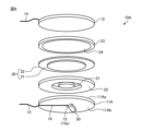
- FIG. 1 is an exploded perspective view schematically showing the configuration of an acoustic sensor according to a first embodiment.
- FIG. 2 is a plan view schematically showing a part of the acoustic sensor according to the first embodiment.
- FIG. 3 is a sectional view taken along line III-III' in FIG. Note that in FIG. 2, the support substrate 11 and the cover member 12 are omitted, and the first connection member 21 and the second connection member 23 are shown with diagonal lines.
- the acoustic sensor 10 includes a piezoelectric plate 30, a support substrate 11, a cover member 12, signal lines 13 and 14, a first connection member 21, and a first insulating member 22. , a second connecting member 23 and a second insulating member 24.
- the first connecting member 21, the first insulating member 22, the piezoelectric plate 30, the second connecting member 23, the second insulating member 24, and the cover member 12 are stacked in this order.
- the piezoelectric plate 30 is a sensor element that converts vibrations of a detected object (for example, a human being) into a corresponding electrical signal.
- the piezoelectric plate 30 includes a piezoelectric element 31 and a conductive plate 32.
- the conductor plate 32 is a plate-shaped member made of a conductor such as a metal material, and has a first surface 32a and a second surface 32b opposite to the first surface 32a.
- the piezoelectric element 31 is provided on the second surface 32b of the conductive plate 32.
- piezoelectric ceramics such as PZT are used, for example.
- the cover member 12 is arranged facing the first surface 32a of the conductor plate 32.
- the cover member 12 is a plate-shaped member made of a conductive material such as a metal material, for example.
- the cover member 12 is a member that transmits vibrations of a detected object (not shown) to the piezoelectric plate 30, and is made of a material that does not substantially undergo compressive deformation. Note that the cover member 12 may be in direct contact with the detected object, or may be in contact with the detected object through another member such as a protective layer.
- the first connecting member 21 and the first insulating member 22 are provided between the piezoelectric plate 30 and the support substrate 11 in the third direction Dz.
- the first connection member 21 is a columnar member, and is provided between the piezoelectric element 31 and the support substrate 11.
- the first connecting member 21 contacts the piezoelectric element 31 at one end in the third direction Dz, and contacts the support substrate 11 at the other end in the third direction Dz.
- the first connection member 21 is made of a conductor and electrically connects the piezoelectric element 31 and the support substrate 11.
- the first insulating member 22 is formed of an insulator and is provided between the second surface 32b of the conductive plate 32 and the support substrate 11 at the outer edge of the second surface 32b of the conductive plate 32. Further, the first insulating member 22 is arranged to overlap with a part of the outer edge of the piezoelectric element 31.
- the first insulating member 22 is an annular member having an opening OP in the center, and the first connecting member 21 is provided at a position overlapping the opening OP of the first insulating member 22. Note that the first insulating member 22 may be arranged without overlapping the outer edge of the piezoelectric element 31.
- the second connecting member 23 and the second insulating member 24 are provided between the piezoelectric plate 30 and the cover member 12 in the third direction Dz.
- the second connection member 23 is made of a conductor and electrically connects the conductor plate 32 and the cover member 12.
- the second connection member 23 is an annular member and is provided at the outer edge of the first surface 32a of the conductor plate 32.
- One end side of the second connecting member 23 in the third direction Dz is in contact with the cover member 12
- the other end side of the second connecting member 23 in the third direction Dz is in contact with the first surface 32 a of the conductor plate 32 .
- the second insulating member 24 is formed of an insulator and is provided between the first surface 32a of the conductive plate 32 and the cover member 12 at the center of the first surface 32a of the conductive plate 32.
- the second insulating member 24 is provided closer to the center than the second connecting member 23 and is disposed within a region surrounded by the second connecting member 23 .
- each member of the acoustic sensor 10 has a circular shape in plan view. It is provided concentrically with respect to the center 32c of the conductive plate 32.
- the diameter of the first connecting member 21 is smaller than the diameter of the piezoelectric element 31.
- the outer diameter of the first insulating member 22 is approximately the same as the diameter of the conductive plate 32.
- the first insulating member 22 is provided along the entire outer edge of the second surface 32 b of the conductor plate 32 and is arranged to surround the first connecting member 21 .
- the diameter of the opening OP of the first insulating member 22 (inner diameter of the first insulating member 22) is larger than the diameter of the first connecting member 21. That is, the first insulating member 22 is provided apart from the first connecting member 21 in the radial direction. Furthermore, the inner edge of the first insulating member 22 that forms the opening OP is provided to cover the entire outer edge of the piezoelectric element 31 .
- the second connection member 23 is provided along the entire outer edge of the first surface 32a of the conductor plate 32.
- the outer diameter of the second connecting member 23 is approximately the same as the diameter of the conductive plate 32.
- the inner diameter of the second connecting member 23 is larger than the diameter of the first connecting member 21 and the diameter of the piezoelectric element 31.
- the diameter of the second insulating member 24 is approximately equal to the inner diameter of the second connecting member 23.
- the second insulating member 24 is provided in a region that overlaps with the opening OP of the piezoelectric element 31, the first connecting member 21, and the first insulating member 22 in plan view.
- the outer periphery of the second insulating member 24 is provided in contact with the inner periphery of the second connecting member 23 .
- the diameter of the second insulating member 24 may be smaller than the inner diameter of the second connecting member 23, and the outer periphery of the second insulating member 24 has a space with the inner periphery of the second connecting member 23. You can do it and stay away.
- the diameter of the support substrate 11 and the diameter of the cover member 12 are equivalent to the diameter of the conductor plate 32 of the piezoelectric plate 30.
- the present invention is not limited thereto, and the diameter of the support substrate 11 and the diameter of the cover member 12 may be larger than the diameter of the conductor plate 32 of the piezoelectric plate 30. Further, the diameter of the support substrate 11 and the diameter of the cover member 12 are the same, but may be different diameters.
- the first connecting member 21 is harder than the first insulating member 22 .
- the material used for the first connection member 21 is carbon-based silicone, urethane foam, polybutadiene, or the like.
- the material of the first connecting member 21 is a closed foam structure.
- the hardness of the first connecting member 21 is approximately Shore hardness A70.
- the volume resistivity of the first connecting member 21 is about 1 ⁇ 10 ⁇ 2 ( ⁇ m) or more and 1 ⁇ 10 2 ( ⁇ m) or less.
- the first insulating member 22 may be made of a PET film, natural rubber (NR), chloroprene rubber (CR), polyethylene (PE), ethylene propylene rubber (EPDM), acrylic, or the like. Moreover, it is preferable that the material of the first insulating member 22 is a closed foam structure.
- the hardness of the first insulating member 22 is approximately Shore hardness A20.
- the volume resistivity of the first insulating member 22 is about 1 ⁇ 10 ⁇ 26 ( ⁇ m) or more and 1 ⁇ 10 10 ( ⁇ m) or less.
- the second connecting member 23 is made of the same material as the first connecting member 21 described above, and the second insulating member 24 is made of the same material as the first insulating member 22 described above. That is, the hardness of the second connecting member 23 is harder than the hardness of the second insulating member 24.
- the material example, hardness, and volume resistivity of the second connection member 23 are the same as those of the first connection member 21 described above, and repeated explanation will be omitted. Further, the material example, hardness, and volume resistivity of the second insulating member 24 are the same as those of the first insulating member 22 described above, and repeated explanation will be omitted.
- the second connecting member 23 may be made of the same material as the first connecting member 21, or may be made of a different material.
- the second insulating member 24 may be made of the same material as the first insulating member 22, or may be made of a different material.
- the second insulating member 24 may be formed of an air layer.
- the second connection member 23 which is harder than the second insulating member 24, is formed in an annular shape along the outer edge of the conductor plate 32.
- the first insulating member 22 is provided in an area overlapping with the second connecting member 23, and the first connecting member 21, which is harder than the first insulating member 22, is provided in the center of the piezoelectric element 31. provided. Therefore, the center part of the piezoelectric element 31 is supported by the first insulating member 22 and its displacement is suppressed, and the outer edge side of the conductive plate 32 and the outer edge side of the piezoelectric element 31 are elastically deformed by the first insulating member 22. The piezoelectric element 31 is more easily displaced than the center part. Therefore, when the displacement of the cover member 12 is transmitted through the second connection member 23, the outer edge side of the conductor plate 32 and the outer edge side of the piezoelectric element 31 are displaced, and the piezoelectric element 31 is deflected and deformed.
- the piezoelectric element 31 outputs an electrical signal according to the deformation.
- the electrical signal from the piezoelectric element 31 is output to an external terminal (for example, the detection circuits 50 and 50A (see FIGS. 6 and 12)) via the first connection member 21, the support substrate 11, and the signal line 13. Further, the electrical signal from the conductor plate 32 is output to the external terminal via the second connection member 23, the cover member 12, and the signal line 14.
- the first connecting member 21 supports the center portion of the piezoelectric plate 30, and the second connecting member 23 transmits the vibration of the detected object to the outer edge side of the piezoelectric plate 30.
- the first connecting member 21 and the second connecting member 23 also serve as electrical connecting members that output electrical signals from the piezoelectric plate 30 to the outside. Therefore, there is no need to connect a cable to the piezoelectric element 31 and the conductive plate 32 for extracting the electric signal to the outside. As a result, it is not necessary to form a through hole in the support substrate 11 and the cover member 12 for passing the cable through. Therefore, the acoustic sensor 10 can have a simpler configuration than when a cable is connected to the piezoelectric plate 30. As a result, the overall configuration of the acoustic sensor 10 including the wiring connected to the piezoelectric plate 30 and external circuits (for example, the detection circuit 50 (see FIG. 6, etc.)) can be made smaller.
- the first surface 32a side of the conductor plate 32 has the second connection member 23, the second insulating member 24, and the cover member. 12 allows for easy sealing. Further, the second surface 32b side of the conductor plate 32 can be easily sealed by the first connecting member 21, the first insulating member 22, and the support substrate 11. Therefore, the acoustic sensor 10 can have a liquid-tight structure in which both sides of the piezoelectric plate 30 are sealed, if necessary.
- the second connecting member 23 which is harder than the second insulating member 24, is formed in an annular shape.
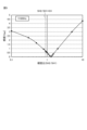
- FIG. 4 is a graph showing the relationship between frequency and sensitivity of the acoustic sensor according to the example for each hardness ratio between the connecting member and the insulating member.
- FIG. 5 is a graph showing the relationship between the hardness ratio of the connecting member and the insulating member and the sensitivity of the acoustic sensor according to the example.
- the frequency in FIGS. 4 and 5 is the drive frequency of the displacement given to the cover member 12.
- the hardness ratio in FIGS. 4 and 5 is the ratio of the hardness of the first insulating member 22 (hereinafter referred to as Shore hardness SH2) to the hardness of the first connecting member 21 (hereinafter referred to as Shore hardness SH1) ( SH2/SH1). Note that the hardness and hardness ratio of the second connecting member 23 and the second insulating member 24 are the same as those of the first connecting member 21 and the first insulating member 22, respectively.
- the diameter of the piezoelectric plate 30 (the diameter of the conductor plate 32) was set to 15 mm.
- the first connecting member 21 is made of a conductive material having a diameter of 9 mm, a thickness of 1 mm, and a shore hardness of A70, for example.
- the first insulating member 22 had an outer diameter of 20 mm, an inner diameter of 10 mm, a thickness of 1 mm, and was made of an insulating material with a Shore hardness of A20.
- the second connecting member 23 is made of, for example, an electrically conductive material with an outer diameter of 20 mm, an inner diameter of 10 mm, a thickness of 1 mm, and a Shore hardness of A70.
- the second insulating member 24 had a diameter of 9 mm, a thickness of 1 mm, and was made of an insulating material with a Shore hardness of A20.
- the support substrate 11 and the cover member 12 were each metal plates with a diameter of 20 mm and a thickness of 0.5 mm.
- FIG. 4 shows the sensitivity (output voltage) of the piezoelectric plate 30 when the hardness ratio SH2/SH1 is different from 0.5, 1.0, and 2.0 in the acoustic sensor 10 according to the example.
- the piezoelectric plate 30 exhibits constant sensitivity (output voltage) to changes in frequency.
- the piezoelectric plate 30 exhibits different sensitivities (output voltages) for each hardness ratio SH2/SH1.
- FIG. 4 shows the sensitivity (output voltage) of the piezoelectric plate 30 when the frequency is constant at 505 Hz.
- the sensitivity (output voltage) changes depending on the change in the hardness ratio SH2/SH1.
- SH2/SH1 is SH2/SH1>1, that is, when the hardness of the first insulating member 22 is harder than the hardness of the first connecting member 21, the sensitivity (output voltage) increases as the hardness ratio SH2/SH1 increases. growing.
- SH2/SH1>1 the piezoelectric element 31 may be deformed in the tensile direction, which may reduce durability.
- the hardness ratio SH2/SH1 0.9.
- FIG. 6 is an exploded perspective view schematically showing the configuration of an acoustic sensor according to the second embodiment.
- FIG. 7 is a sectional view schematically showing the configuration of an acoustic sensor according to the second embodiment.
- the support substrate 11A is an insulating substrate formed of an insulator.
- a printed wiring board is used as the support substrate 11A, for example.
- the support substrate 11A has a base made of an insulating resin material and has a conductive member 15a inside.
- the support substrate 11A has contacts that penetrate through the front surface 11Aa (the surface facing the piezoelectric element 31) and the back surface 11Ab (the surface opposite to the surface facing the piezoelectric element 31).
- a hole 15 is provided.
- the conductive member 15a is filled in the contact hole 15 and electrically connects the front surface 11Aa side and the back surface 11Ab side.
- One end side of the contact hole 15 is electrically connected to the first connecting member 21 on the surface 11Aa of the support substrate 11A.
- the other end side of the contact hole 15 (conductive member 15a) is electrically connected to the connection wiring 16 on the back surface 11Ab of the support substrate 11A.
- the piezoelectric element 31 of the piezoelectric plate 30 is electrically connected to the back surface 11Ab side of the support substrate 11A via the first connection member 21 and the contact hole 15 (conductive member 15a).
- the acoustic sensor 10A of the second embodiment has a detection circuit 50 (not shown in FIG. 7) provided on the back surface 11Ab of the support substrate 11A.
- the detection circuit 50 is configured of, for example, an IC (Integrated Circuit), and is a circuit that processes electrical signals from the piezoelectric plate 30.
- the support substrate 11A by using an insulating substrate as the support substrate 11A, the support substrate 11A has a substrate supporting the piezoelectric plate 30, and various wirings such as the connection wiring 16 and components such as the detection circuit 50 mounted thereon. It also serves as a wiring board. Therefore, the acoustic sensor 10A can achieve miniaturization of the entire configuration including the detection circuit 50.
- the support substrate 11A is not limited to the configuration having the connection wiring 16, the contact hole 15, and the conductive member 15a, but may have wiring provided in an inner layer, a plurality of contact holes, and a conductive member. Further, the back surface 11Ab of the support substrate 11A is not limited to the detection circuit 50, and other mounted components or circuits may be provided.
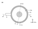
- FIG. 8 is an exploded perspective view schematically showing the configuration of an acoustic sensor according to the third embodiment.
- FIG. 9 is a plan view schematically showing the configuration of a support substrate according to the third embodiment.
- FIG. 10 is a plan view schematically showing the configuration of the back side of the support substrate according to the third embodiment.
- FIG. 11 is a sectional view taken along line XI-XI' in FIG.
- the acoustic sensor 10B includes a third connection member 25 that electrically connects the support substrate 11B and the cover member 12 will be described. do.
- the support substrate 11B and the cover member 12 have a larger diameter (outer shape) than the conductor plate 32 of the piezoelectric plate 30.
- the support substrate 11B is an insulating substrate made of an insulator similarly to the second embodiment.
- the piezoelectric element 31 of the piezoelectric plate 30 is electrically connected to the back surface 11Bb side of the support substrate 11B via the first connection member 21 and the contact hole 15 (conductive member 15a). Ru.
- cover member 12 is a film-like member made of a conductive material.
- the conductor plate 32 of the piezoelectric plate 30 is electrically connected to the cover member 12 via the second connection member 23.
- the third connection member 25 is formed of a conductor, is provided outside the outer periphery of the conductor plate 32 of the piezoelectric plate 30, and electrically connects the support substrate 11B and the cover member 12. More specifically, as shown in FIG. 11, the third connecting member 25 has an annular shape surrounding the piezoelectric plate 30, the first connecting member 21, the first insulating member 22, the second connecting member 23, and the second insulating member 24. be.
- the third connection member 25 is provided in an annular shape along the entire outer edge of the support substrate 11B. Further, the third connecting member 25 is arranged apart from the outer periphery of the conductive plate 32 of the piezoelectric plate 30, the first insulating member 22, and the second connecting member 23 with a space therebetween.
- One end side of the third connection member 25 in the third direction Dz is in contact with the cover member 12, and the other end side of the third connection member 25 in the third direction Dz is electrically connected to the surface 11Ba side of the support substrate 11B via the connection wiring 18. connected.
- connection wiring 18 is provided in a ring shape along the area overlapping with the third connection member 25, that is, along the entire outer edge of the surface 11Ba of the support substrate 11B.
- a contact hole 17 passing through the front surface 11Ba and the back surface 11Bb is provided at a position overlapping the connection wiring 18 of the support substrate 11B.
- the conductive member 17a is filled in the contact hole 17 and electrically connects the front surface 11Ba side and the back surface 11Bb side.
- the first connection member 21 is electrically connected to the back surface 11Bb side of the support substrate 11B via the contact hole 15 (conductive member 15a) at the center of the support substrate 11B. be done.
- a detection circuit 50A is provided on the back surface 11Bb of the support substrate 11B.
- the third connection member 25 is electrically connected to the detection circuit 50A via the contact hole 17 (conductive member 17a) and wiring provided on the back surface 11Bb.
- the first connecting member 21 is electrically connected to the detection circuit 50A via the contact hole 15 (conductive member 15a) and wiring provided on the back surface 11Bb. Note that a detailed configuration example of the detection circuit 50A will be described later with reference to FIG.
- the piezoelectric element 31 of the piezoelectric plate 30 is electrically connected to the detection circuit 50A on the back surface 11Bb of the support substrate 11B via the first connection member 21 and the contact hole 15 (conductive member 15a).
- the conductive plate 32 of the piezoelectric plate 30 connects to the detection circuit on the back surface 11Bb of the support substrate 11B via the second connection member 23, the cover member 12, the third connection member 25, the connection wiring 18, and the contact hole 17 (conductive member 17a). It is electrically connected to 50A.
- the cover member 12 is formed of a deformable film-like member, so the vibration of the detected object is transmitted to the cover member 12 and the second connecting member 23. It is transmitted well to the piezoelectric plate 30 via.
- the support substrate 11B has a connecting portion 19 that protrudes radially outward from the outer periphery.
- the detection circuit 50A is electrically connected to an external control board via a plurality of connection wires 16 provided in the connection portion 19.
- the plurality of connection wiring lines 16 include, for example, a ground line 16a that supplies a ground potential to the piezoelectric plate 30, a signal line 16b that outputs a signal from the piezoelectric plate 30 via the detection circuit 50A, and a power supply potential to the detection circuit 50A. It includes the power supply line 16c and the like.
- FIG. 12 is a circuit diagram showing a configuration example of a detection circuit of an acoustic sensor according to the third embodiment.
- the detection circuit 50A includes a protection circuit 51, an active filter 52, a constant voltage circuit 53, and a signal processing circuit 54.
- the protection circuit 51 is a circuit for protecting the piezoelectric plate 30 from overvoltage and the like, and includes diodes 51a and 51b electrically connected to the piezoelectric plate 30.
- the active filter 52 is a filter circuit that passes signals in a predetermined frequency range among the signals from the piezoelectric plate 30, and includes an amplifier 52a, resistive elements 52b and 52c, and a capacitor 52d.
- active filter 52 is configured as a low-pass filter.
- the active filter 52 may be a high-pass filter or a band-pass filter.
- the present invention is not limited to the active filter 52, and a passive filter may be provided, or the amplifier 52a may be simply connected.
- the number of active filters 52 is not limited to one stage, and may be connected in multiple stages.
- the constant voltage circuit 53 is a circuit that supplies a constant voltage to the amplifier 52a of the active filter 52, and includes resistance elements 53a and 53b.
- the signal processing circuit 54 is a circuit that processes signals from the piezoelectric plate 30, and includes an A/D conversion circuit 54a and a signal processing section 54b.
- the A/D conversion circuit 54a is a circuit that converts an analog signal from the piezoelectric plate 30 into a digital signal.
- the signal processing section 54b is a circuit that receives the digital signal from the A/D conversion circuit 54a and performs signal processing such as amplification and filtering.
- the protection circuit 51, active filter 52, and constant voltage circuit 53 of the detection circuit 50A are provided on the back surface 11Bb of the support substrate 11B, and the signal processing circuit 54 is provided on an external control board.
- the signal line 16b (see FIG. 10) provided in the connection portion 19 is provided as a wiring for extracting an analog signal from the active filter 52.
- the present invention is not limited to this, and all of the detection circuit 50A including the signal processing circuit 54 may be provided on the back surface 11Bb of the support substrate 11B.
- the signal line 16b (see FIG. 10) provided in the connection section 19 is configured not as an analog signal output but as a plurality of digital I/F signal input/output terminals.
- a serial port such as SPI, I2C, USB, or UART, or a parallel port is provided as a digital I/F signal input/output terminal.
- the cover member 12 is electrically connected to the support substrate 11B via the third connection member 25. Therefore, the detection circuit 50A and various wirings can be provided together on the support substrate 11B, and the entire acoustic sensor 10B including the detection circuit 50A and various wirings can be miniaturized.
- FIG. 13 is an explanatory diagram for explaining a stethoscope according to the fourth embodiment.
- a stethoscope 100 according to the fourth embodiment includes a chest piece 101, a Y-shaped tube 103, two ear tubes 104, and two ear tips 105.
- the chest piece 101 has a housing 101a and a contact portion 101b.
- the acoustic sensors 10, 10A, and 10B are incorporated inside the housing 101a.
- the contact portion 101b is a member that comes into contact with a living body (for example, a human being), and is configured to transmit vibrations of the living body to the cover member 12 (see FIG. 1, etc.).
- the chest piece 101 of the stethoscope 100 includes a signal processing circuit, an amplifier, a speaker, etc. that converts electrical signals from the piezoelectric plates 30 of the acoustic sensors 10, 10A, 10B into audio.
- the stethoscope 100 may include a wireless communication module that transmits electrical signals from the piezoelectric plates 30 of the acoustic sensors 10, 10A, and 10B to the outside as necessary.
- the Y-shaped tube 103 connects the chest piece 101 and the two Eustachian tubes 104.
- Two ear tips 105 are connected to each of the two ear canals 104. Sound generated based on electrical signals from the piezoelectric plates 30 of the acoustic sensors 10, 10A, 10B is output to the outside via the two ear tips 105.
- the chest piece 101 can be made smaller. Furthermore, since the acoustic sensors 10, 10A, and 10B can have a liquid-tight structure in which both sides of the piezoelectric plate 30 are sealed, the stethoscope 100 having the acoustic sensors 10, 10A, and 10B is free from moisture and disinfectant infiltration. Damage to the piezoelectric plate 30 and the detection circuits 50 and 50A can be suppressed.
- the stethoscope 100 having the acoustic sensors 10, 10A, and 10B has been described, but the acoustic sensors 10, 10A, and 10B can be applied to other devices than the stethoscope 100.
- the acoustic sensors 10, 10A, and 10B may be applied to a heart sound sensor that is kept attached to a living body for a long time in order to monitor heart sounds.
- the piezoelectric plate 30, the support substrate 11, and the cover member 12 have a circular shape in a plan view, but the piezoelectric plate 30, the support substrate 11, and the cover member 12 have a rectangular shape, a polygonal shape, etc. etc., other shapes may also be used.
Landscapes
- Physics & Mathematics (AREA)
- Acoustics & Sound (AREA)
- Health & Medical Sciences (AREA)
- Life Sciences & Earth Sciences (AREA)
- Engineering & Computer Science (AREA)
- Biomedical Technology (AREA)
- Heart & Thoracic Surgery (AREA)
- Medical Informatics (AREA)
- Molecular Biology (AREA)
- Surgery (AREA)
- Animal Behavior & Ethology (AREA)
- General Health & Medical Sciences (AREA)
- Public Health (AREA)
- Veterinary Medicine (AREA)
- Piezo-Electric Transducers For Audible Bands (AREA)
Abstract
音響センサ(10)は、第1面と、第1面と反対側の第2面とを有する導体板(32)と、導体板(32)の第2面に設けられた圧電素子(31)と、を含む圧電板(30)と、導体板(32)の第1面に対向して配置されたカバー部材(12)と、導体板(32)の第2面及び圧電素子(31)に対向して配置された支持基板(11)と、導体で形成され、圧電素子(31)と支持基板(11)との間に設けられ、圧電素子(31)と支持基板(11)とを電気的に接続する第1接続部材(21)と、絶縁体で形成され、導体板(32)の第2面の外縁で、導体板(32)の第2面と支持基板(11)との間に設けられた第1絶縁部材(22)と、導体で形成され、導体板(32)の第1面の外縁に設けられ、導体板(32)とカバー部材(12)とを電気的に接続する第2接続部材(23)と、を有する。
Description
本発明は、音響センサ及び聴診器に関する。
特許文献1には、圧電板を用いた生体音響センサ及びそれを用いた聴診器について開示されている。特許文献1に記載されている聴診器では、生体に接触する接触面を備えた振動板と、振動板に対向配置され、振動板の振動を電気信号に変換する圧電板と、圧電板の中央部に設けられ振動板の振動を圧電板に伝達する振動伝達部材と、を有する。
特許文献1では、振動板及び圧電板のそれぞれを支持する支持部材が設けられ、さらに、圧電板の電気信号を外部に取り出すためのケーブルが接続されている。聴診器の筐体にはケーブルを通すための開口を設ける必要がある。このため特許文献1では、振動板や圧電板の形状及び配置の自由度が低下する可能性がある。
本発明は、簡易な構成で、良好に振動を検出することができる音響センサ及び聴診器を提供することを目的とする。
本発明の一側面の音響センサは、第1面と、前記第1面と反対側の第2面とを有する導体板と、前記導体板の前記第2面に設けられた圧電素子と、を含む圧電板と、前記導体板の前記第1面に対向して配置されたカバー部材と、前記導体板の前記第2面及び前記圧電素子に対向して配置された支持基板と、導体で形成され、前記圧電素子と前記支持基板の間に設けられ、前記圧電素子と前記支持基板とを電気的に接続する第1接続部材と、絶縁体で形成され、前記導体板の前記第2面の外縁で、前記導体板の前記第2面と前記支持基板との間に設けられた第1絶縁部材と、導体で形成され、前記導体板の前記第1面の外縁に設けられ、前記導体板と前記カバー基板とを電気的に接続する第2接続部材と、を有する。
本発明の一側面の聴診器は、上記の音響センサと、前記音響センサが内蔵されたチェストピースと、前記チェストピースに接続され、前記音響センサの前記圧電板からの電気信号に基づいて生成された音を外部に出力するイヤーチップと、を有する。
本発明の音響センサ及び聴診器によれば、簡易な構成で、良好に振動を検出することができる。
以下に、本発明の音響センサ及び聴診器の実施の形態を図面に基づいて詳細に説明する。なお、この実施の形態により本発明が限定されるものではない。各実施の形態は例示であり、異なる実施の形態で示した構成の部分的な置換又は組み合わせが可能であることは言うまでもない。第2実施形態以降では第1実施形態と共通の事柄についての記述を省略し、異なる点についてのみ説明する。特に、同様の構成による同様の作用効果については実施形態毎には逐次言及しない。
(第1実施形態)
図1は、第1実施形態に係る音響センサの構成を模式的に示す分解斜視図である。図2は、第1実施形態に係る音響センサの一部を模式的に示す平面図である。図3は、図2のIII-III’断面図である。なお、図2では支持基板11及びカバー部材12を省略して示しており、第1接続部材21及び第2接続部材23に斜線を付して示している。
図1は、第1実施形態に係る音響センサの構成を模式的に示す分解斜視図である。図2は、第1実施形態に係る音響センサの一部を模式的に示す平面図である。図3は、図2のIII-III’断面図である。なお、図2では支持基板11及びカバー部材12を省略して示しており、第1接続部材21及び第2接続部材23に斜線を付して示している。
図1及び図3に示すように、音響センサ10は、圧電板30と、支持基板11と、カバー部材12と、信号線13、14と、第1接続部材21と、第1絶縁部材22と、第2接続部材23と、第2絶縁部材24と、を有する。支持基板11の上に、第1接続部材21及び第1絶縁部材22、圧電板30、第2接続部材23及び第2絶縁部材24、カバー部材12の順に積層される。
なお、以下の説明において、支持基板11の表面11aを含む平面に平行な面内の一方向を第1方向Dxとする。また、表面11aを含む平面に平行な面内において第1方向Dxと直交する方向を第2方向Dyとする。また、第1方向Dx及び第2方向Dyのそれぞれと直交する方向を第3方向Dzとする。第3方向Dzは、支持基板11の表面11aの法線方向である。また、本明細書において、平面視とは、第3方向Dzから見たときの位置関係を示す。
圧電板30は、被検出体(例えば、人間)の振動を対応する電気信号に変換するセンサ素子である。具体的には、図3に示すように、圧電板30は、圧電素子31と、導体板32と、を有する。導体板32は、金属材料などの導体で形成された板状の部材であり、第1面32aと、第1面32aの反対側の第2面32bと、を有する。圧電素子31は、導体板32の第2面32bに設けられる。圧電素子31は、例えばPZT等の圧電セラミックスが用いられる。
カバー部材12は、導体板32の第1面32aに対向して配置される。カバー部材12は、例えば金属材料等の導電性を有する材料で形成された板状の部材である。カバー部材12は、被検出体(図示しない)の振動を圧電板30に伝達する部材であり、実質的に圧縮変形しない材料で形成される。なお、カバー部材12は、被検出体と直接接触してもよいし、保護層などの他の部材を介して被検出体と接触してもよい。
支持基板11は、導体板32の第2面32b及び圧電素子31に対向して配置される。支持基板11は、表面11a(圧電素子31と対向する面)と、表面11aの反対側の裏面11b(圧電素子31と対向する面の反対側の面)と、を有する板状の部材である。支持基板11は、導体であり、例えば金属材料等の導電性を有する材料で形成される。支持基板11は、圧電板30よりも高い剛性を有し、被検出体の振動により変形しない、あるいは被検出体の振動による変形を抑制するように構成される。
第1接続部材21及び第1絶縁部材22は、第3方向Dzで、圧電板30と支持基板11との間に設けられる。具体的には、第1接続部材21は、柱状の部材であり、圧電素子31と支持基板11との間に設けられる。第1接続部材21は、第3方向Dzの一端側が圧電素子31と接し、第3方向Dzの他端側が支持基板11と接する。第1接続部材21は、導体で形成され、圧電素子31と支持基板11とを電気的に接続する。
第1絶縁部材22は、絶縁体で形成され、導体板32の第2面32bの外縁で、導体板32の第2面32bと支持基板11との間に設けられる。また、第1絶縁部材22は、圧電素子31の外縁の一部とも重なって配置される。第1絶縁部材22は、中央部に開口OPが設けられた環状の部材であり、第1接続部材21は、第1絶縁部材22の開口OPと重なる位置に設けられる。なお、第1絶縁部材22は、圧電素子31の外縁と重ならないで配置されてもよい。
第2接続部材23及び第2絶縁部材24は、第3方向Dzで、圧電板30とカバー部材12との間に設けられる。第2接続部材23は、導体で形成され、導体板32とカバー部材12とを電気的に接続する。具体的には、第2接続部材23は、環状の部材であり、導体板32の第1面32aの外縁に設けられる。第2接続部材23の第3方向Dzの一端側はカバー部材12と接し、第2接続部材23の第3方向Dzの他端側は導体板32の第1面32aと接する。
第2絶縁部材24は、絶縁体で形成され、導体板32の第1面32aの中央部で、導体板32の第1面32aとカバー部材12との間に設けられる。第2絶縁部材24は、第2接続部材23よりも中央部側に設けられ、第2接続部材23で囲まれた領域内に配置される。
図2に示すように、音響センサ10の各部材(圧電板30、第1接続部材21、第1絶縁部材22、第2接続部材23、第2絶縁部材24)は、平面視で円形状であり、導体板32の中心32cに対して同心円状に設けられる。
第1接続部材21の直径は、圧電素子31の直径よりも小さい。第1絶縁部材22の外径は、導体板32の直径と概ね同等である。第1絶縁部材22は、導体板32の第2面32bの外縁の全周に沿って設けられ、第1接続部材21を囲んで配置される。第1絶縁部材22の開口OPの直径(第1絶縁部材22の内径)は、第1接続部材21の直径よりも大きい。すなわち、第1絶縁部材22は、径方向で第1接続部材21と離れて設けられる。また、第1絶縁部材22の開口OPを形成する内縁は、圧電素子31の外縁の全周を覆って設けられる。
第2接続部材23は、導体板32の第1面32aの外縁の全周に沿って設けられる。第2接続部材23の外径は、導体板32の直径と概ね同等である。第2接続部材23の内径は、第1接続部材21の直径及び圧電素子31の直径よりも大きい。本実施形態では、第2絶縁部材24の直径は、第2接続部材23の内径と概ね同等である。第2絶縁部材24は、平面視で圧電素子31、第1接続部材21及び第1絶縁部材22の開口OPと重なる領域に設けられる。第2絶縁部材24の外周は第2接続部材23の内周と接して設けられる。ただし、これに限定されず、第2絶縁部材24の直径は第2接続部材23の内径よりも小さくてもよく、第2絶縁部材24の外周は第2接続部材23の内周と空間を有して離れていてもよい。
なお、図2では図示を省略するが、図1及び図3に示すように、支持基板11の直径及びカバー部材12の直径は、圧電板30の導体板32の直径と同等である。ただし、これに限定されず、支持基板11の直径及びカバー部材12の直径は、圧電板30の導体板32の直径よりも大きくてもよい。また、支持基板11の直径とカバー部材12の直径は、同等であるが、異なる直径であってもよい。
次に、第1接続部材21、第1絶縁部材22、第2接続部材23及び第2絶縁部材24の材料例について説明する。第1接続部材21の硬さは、第1絶縁部材22の硬さよりも硬い。具体的には、第1接続部材21の材料は、カーボン系シリコーン、ウレタンフォーム、ポリブタジエンなどが用いられる。また、第1接続部材21の材料は、独立発泡構造体であることが好ましい。第1接続部材21の硬さは、ショア硬度A70程度である。第1接続部材21の体積抵抗率は、1×10⁻²(Ω・m)以上、1×10²(Ω・m)以下程度である。
第1絶縁部材22の材料は、PET系フィルム、天然ゴム(NR)、クロロプレンゴム(CR)、ポリエチレン(PE)、エチレンプロピレンゴム(EPDM)、アクリルなどが用いられる。また、第1絶縁部材22の材料は、独立発泡構造体であることが好ましい。第1絶縁部材22の硬さは、ショア硬度A20程度である。第1絶縁部材22の体積抵抗率は、1×10-26(Ω・m)以上、1×10¹⁰(Ω・m)以下程度である。
第2接続部材23は、上述した第1接続部材21と同様の材料が用いられ、第2絶縁部材24は、上述した第1絶縁部材22と同様の材料が用いられる。すなわち、第2接続部材23の硬さは、第2絶縁部材24の硬さよりも硬い。第2接続部材23の材料例、硬さ及び体積抵抗率は、上述した第1接続部材21と同様であり、繰り返しの説明は省略する。また、第2絶縁部材24の材料例、硬さ及び体積抵抗率は、上述した第1絶縁部材22と同様であり、繰り返しの説明は省略する。なお、第2接続部材23は、第1接続部材21と同じ材料で形成されていてもよいし、異なる材料で形成されていてもよい。また、第2絶縁部材24は、第1絶縁部材22と同じ材料で形成されていてもよいし、異なる材料で形成されていてもよい。例えば、第2絶縁部材24は空気層で形成されていてもよい。
このような構成により、導体板32の第1面32a側では、第2絶縁部材24よりも硬い第2接続部材23が導体板32の外縁に沿って環状に形成される。被検出体の振動によりカバー部材12が振動し、第3方向Dzに繰り返し変位すると、カバー部材12の変位は、主に、第2絶縁部材24よりも硬い第2接続部材23を介して圧電板30の外縁、すなわち導体板32の外縁に伝わる。
導体板32の第2面32b側では、第2接続部材23と重なる領域に第1絶縁部材22が設けられ、圧電素子31の中央部に第1絶縁部材22よりも硬い第1接続部材21が設けられる。したがって、圧電素子31の中央部は、第1絶縁部材22に支持されて変位が抑制され、導体板32の外縁側及び圧電素子31の外縁側は、第1絶縁部材22が弾性変形することで圧電素子31の中央部よりも変位しやすい。したがって、カバー部材12の変位が第2接続部材23を介して伝わると、導体板32の外縁側及び圧電素子31の外縁側が変位し、圧電素子31がたわみ変形する。
圧電素子31は変形に応じた電気信号を出力する。圧電素子31からの電気信号は、第1接続部材21、支持基板11及び信号線13を介して外部端子(例えば検出回路50、50A(図6、図12参照))に出力される。また、導体板32からの電気信号は、第2接続部材23、カバー部材12及び信号線14を介して外部端子に出力される。
このように、第1接続部材21は圧電板30の中央部を支持し、第2接続部材23は被検出体の振動を圧電板30の外縁側に伝える。さらに、第1接続部材21及び第2接続部材23は、圧電板30からの電気信号を外部に出力する電気的接続部材を兼ねる。したがって、圧電素子31及び導体板32には、電気信号を外部に取り出すためのケーブルを接続する必要がない。この結果、支持基板11及びカバー部材12には、ケーブルを通すための貫通孔を形成する必要がない。したがって、音響センサ10は、圧電板30にケーブルが接続された場合に比べて、簡易な構成とすることができる。この結果、音響センサ10は、圧電板30に接続される配線や外部回路(例えば検出回路50(図6等参照))を含めた全体の構成の小型化を図ることができる。
また、支持基板11及びカバー部材12にケーブルを通すための貫通孔を形成する必要がないので、導体板32の第1面32a側は、第2接続部材23、第2絶縁部材24及びカバー部材12により、容易に封止することができる。また、導体板32の第2面32b側は、第1接続部材21、第1絶縁部材22及び支持基板11により、容易に封止することができる。したがって、音響センサ10は、必要に応じて、圧電板30の両面とも密封された液密構造が可能となる。
上述したように、導体板32の第1面32a側では、第2絶縁部材24よりも硬い第2接続部材23が環状に形成される。また、導体板32の第2面32b側では第1絶縁部材22よりも硬い第1接続部材21が圧電素子31の中央部に設けられる。これにより、被検出体の振動によりカバー部材12が振動すると、圧電素子31は圧縮方向に変形しやすくなる。したがって、音響センサ10は、圧電素子31を引っ張り方向に変形させる構造に比べて、過剰なたわみ変形に対する圧電素子31の耐性を向上させることができる。
(実施例)
図4は、実施例に係る音響センサの、周波数と感度との関係を、接続部材と絶縁部材との硬度比ごとに示すグラフである。図5は、実施例に係る音響センサの、接続部材と絶縁部材との硬度比と、感度との関係を示すグラフである。
図4は、実施例に係る音響センサの、周波数と感度との関係を、接続部材と絶縁部材との硬度比ごとに示すグラフである。図5は、実施例に係る音響センサの、接続部材と絶縁部材との硬度比と、感度との関係を示すグラフである。
図4及び図5は、各周波数、及び、接続部材と絶縁部材との硬度比ごとの、圧電板30の感度(出力電圧)のシミュレーション結果を示す。図4及び図5における周波数は、カバー部材12に与えた変位の駆動周波数である。また、図4及び図5における硬度比は、第1接続部材21の硬さ(以下、ショア硬度SH1とする)に対する第1絶縁部材22の硬さ(以下、ショア硬度SH2とする)の比(SH2/SH1)を示す。なお、第2接続部材23及び第2絶縁部材24の硬さ及び硬度比は、それぞれ第1接続部材21及び第1絶縁部材22の硬さ及び硬度比と同じものとする。
図4及び図5に示すシミュレーションでは、圧電板30の直径(導体板32の直径)を15mmとした。第1接続部材21は、例えば、直径9mm、厚さ1mmで、ショア硬度がA70の導電性の材料とした。第1絶縁部材22は、外径20mm、内径10mm、厚さ1mmで、ショア硬度がA20の絶縁性の材料とした。
第2接続部材23は、例えば、外径20mm、内径10mm、厚さ1mmで、ショア硬度がA70の導電性の材料とした。第2絶縁部材24は、直径9mm、厚さ1mmで、ショア硬度がA20の絶縁性の材料とした。
支持基板11及びカバー部材12は、それぞれ、直径20mm、厚さ0.5mmの金属板とした。
図4では、実施例に係る音響センサ10において、硬度比SH2/SH1=0.5、1.0、2.0と異ならせた場合の圧電板30の感度(出力電圧)を示す。図4に示すように、圧電板30は、周波数の変化に対して一定の感度(出力電圧)を示す。また、圧電板30は、硬度比SH2/SH1ごとに異なる感度(出力電圧)を示す。
図4では、周波数を505Hz一定とした場合の、圧電板30の感度(出力電圧)を示す。図5に示すように、硬度比SH2/SH1の変化に応じて、感度(出力電圧)が変化する。硬度比SH2/SH1がSH2/SH1>1の領域、すなわち第1絶縁部材22の硬さが第1接続部材21の硬さよりも硬い場合、硬度比SH2/SH1が大きいほど感度(出力電圧)が大きくなる。ただし、SH2/SH1>1では、圧電素子31に引っ張り方向の変形が生じ、耐久性が低下する可能性がある。
比較的高い耐久性が得られるSH2/SH1<1の領域、すなわち第1接続部材21の硬さが第1絶縁部材22の硬さよりも硬い場合では、硬度比SH2/SH1=0.9での感度は、硬度比SH2/SH1=1での感度に比べて、1.4倍程度になる。このように、実施例に係る音響センサ10では、硬度比SH2/SH1<0.9とすることで、圧電素子31の耐久性が向上するとともに、良好な感度(出力電圧)が得られることが示された。
(第2実施形態)
図6は、第2実施形態に係る音響センサの構成を模式的に示す分解斜視図である。図7は、第2実施形態に係る音響センサの構成を模式的に示す断面図である。第2実施形態では、上述した第1実施形態とは異なり、支持基板11Aが絶縁体で形成された絶縁基板である構成について説明する。
図6は、第2実施形態に係る音響センサの構成を模式的に示す分解斜視図である。図7は、第2実施形態に係る音響センサの構成を模式的に示す断面図である。第2実施形態では、上述した第1実施形態とは異なり、支持基板11Aが絶縁体で形成された絶縁基板である構成について説明する。
図6及び図7に示すように、第2実施形態に係る音響センサ10Aにおいて、支持基板11Aは、例えばプリント配線基板が用いられる。支持基板11Aは、絶縁性の樹脂材料を基体とし、内部に導電部材15aを有する。図6及び図7に示す例では、支持基板11Aは、表面11Aa(圧電素子31と対向する面)と、裏面11Ab(圧電素子31と対向する面の反対側の面)と、を貫通するコンタクトホール15が設けられる。導電部材15aはコンタクトホール15内に充填され、表面11Aa側と裏面11Ab側とを電気的に接続する。
コンタクトホール15(導電部材15a)の一端側は、支持基板11Aの表面11Aaで第1接続部材21と電気的に接続される。コンタクトホール15(導電部材15a)の他端側は、支持基板11Aの裏面11Abで接続配線16と電気的に接続される。これにより、圧電板30の圧電素子31は、第1接続部材21及びコンタクトホール15(導電部材15a)を介して、支持基板11Aの裏面11Ab側と電気的に接続される。
図6に示すように、第2実施形態の音響センサ10Aは、支持基板11Aの裏面11Abに設けられた検出回路50(図7では不図示)を有する。検出回路50は、例えばIC(Integrated Circuit)で構成され、圧電板30からの電気信号の信号処理を行う回路である。
本実施形態の音響センサ10Aでは、支持基板11Aとして絶縁基板を用いることにより、支持基板11Aは、圧電板30を支持する基板と、接続配線16等の各種配線や検出回路50等の部品を実装する配線基板とを兼ねる。したがって、音響センサ10Aは、検出回路50を含む全体の構成の小型化を図ることができる。
なお、支持基板11Aは、接続配線16、コンタクトホール15及び導電部材15aを有する構成に限定されず、内層に設けられた配線や、複数のコンタクトホール及び導電部材を有していてもよい。また、支持基板11Aの裏面11Abには、検出回路50に限定されず、他の実装部品や回路が設けられていてもよい。
(第3実施形態)
図8は、第3実施形態に係る音響センサの構成を模式的に示す分解斜視図である。図9は、第3実施形態に係る支持基板の構成を模式的に示す平面図である。図10は、第3実施形態に係る支持基板の、裏面側の構成を模式的に示す平面図である。図11は、図9のXI-XI’断面図である。
図8は、第3実施形態に係る音響センサの構成を模式的に示す分解斜視図である。図9は、第3実施形態に係る支持基板の構成を模式的に示す平面図である。図10は、第3実施形態に係る支持基板の、裏面側の構成を模式的に示す平面図である。図11は、図9のXI-XI’断面図である。
第3実施形態では、上述した第1実施形態及び第2実施形態とは異なり、音響センサ10Bが、支持基板11Bとカバー部材12とを電気的に接続する第3接続部材25を有する構成について説明する。
図8及び図11に示すように、第3実施形態に係る音響センサ10Bにおいて、支持基板11B及びカバー部材12は、圧電板30の導体板32よりも大きい直径(外形形状)を有する。支持基板11Bは、第2実施形態と同様に絶縁体で形成された絶縁基板である。また、第2実施形態と同様に、圧電板30の圧電素子31は、第1接続部材21及びコンタクトホール15(導電部材15a)を介して、支持基板11Bの裏面11Bb側と電気的に接続される。
また、カバー部材12は、導電性を有する材料で形成されたフィルム状の部材である。上述した第1実施形態及び第2実施形態と同様に、圧電板30の導体板32は、第2接続部材23を介して、カバー部材12と電気的に接続される。
第3接続部材25は、導体で形成され、圧電板30の導体板32の外周よりも外側に設けられ、支持基板11Bとカバー部材12とを電気的に接続する。より詳細には、図11に示すように、第3接続部材25は、圧電板30、第1接続部材21、第1絶縁部材22、第2接続部材23及び第2絶縁部材24を囲む環状である。第3接続部材25は、支持基板11Bの外縁の全周に沿って環状に設けられる。また、第3接続部材25は、圧電板30の導体板32、第1絶縁部材22及び第2接続部材23の外周と空間を有して離れて配置される。
第3接続部材25の第3方向Dzの一端側はカバー部材12と接し、第3接続部材25の第3方向Dzの他端側は接続配線18を介して支持基板11Bの表面11Ba側と電気的に接続される。
図9に示すように、接続配線18は、第3接続部材25と重なる領域、すなわち、支持基板11Bの表面11Baの外縁の全周に沿って環状に設けられる。支持基板11Bの接続配線18と重なる位置に、表面11Baと裏面11Bbとを貫通するコンタクトホール17が設けられる。導電部材17aはコンタクトホール17内に充填され、表面11Ba側と、裏面11Bb側とを電気的に接続する。
また、上述した第2実施形態と同様に、第1接続部材21は、支持基板11Bの中央部でコンタクトホール15(導電部材15a)を介して、支持基板11Bの裏面11Bb側と電気的に接続される。
図10に示すように、支持基板11Bの裏面11Bbには、検出回路50Aが設けられる。第3接続部材25は、コンタクトホール17(導電部材17a)及び裏面11Bbに設けられた配線を介して、検出回路50Aと電気的に接続される。また、第1接続部材21は、コンタクトホール15(導電部材15a)及び裏面11Bbに設けられた配線を介して、検出回路50Aと電気的に接続される。なお、検出回路50Aの詳細な構成例は図12にて後述する。
以上のような構成により、圧電板30の圧電素子31は第1接続部材21及びコンタクトホール15(導電部材15a)を介して、支持基板11Bの裏面11Bbの検出回路50Aと電気的に接続される。圧電板30の導体板32は、第2接続部材23、カバー部材12、第3接続部材25、接続配線18及びコンタクトホール17(導電部材17a)を介して、支持基板11Bの裏面11Bbの検出回路50Aと電気的に接続される。なお、第3接続部材25が設けられた構成であっても、カバー部材12は変形可能なフィルム状の部材で形成されているので、被検出体の振動はカバー部材12及び第2接続部材23を介して圧電板30に良好に伝わる。
また、支持基板11Bは、外周から径方向外側に突出する接続部19を有する。検出回路50Aは、接続部19に設けられた複数の接続配線16を介して外部の制御基板と電気的に接続される。複数の接続配線16は、例えば、圧電板30にグランド電位を供給するグランド線16aや、検出回路50Aを介して圧電板30からの信号を出力する信号線16bや、検出回路50Aに電源電位を供給する電源線16c等を含む。
図12は、第3実施形態に係る音響センサの、検出回路の構成例を示す回路図である。図12に示すように、検出回路50Aは、保護回路51、アクティブフィルタ52、定電圧回路53及び信号処理回路54を有する。保護回路51は、圧電板30を過電圧等から保護するための回路であり、圧電板30と電気的に接続されたダイオード51a、51bを有する。
アクティブフィルタ52は、圧電板30からの信号のうち所定の周波数範囲の信号を通過させるフィルタ回路であり、増幅器52a、抵抗素子52b、52c及びコンデンサ52dを有する。図12では、アクティブフィルタ52はローパスフィルタとして構成される。ただし、アクティブフィルタ52はハイパスフィルタ、あるいは、バンドパスフィルタであってもよい。また、アクティブフィルタ52に限定されず、パッシブフィルタが設けられていてもよいし、単に増幅器52aが接続されていてもよい。アクティブフィルタ52の段数も1段に限定されず、複数段接続されていてもよい。
定電圧回路53は、アクティブフィルタ52の増幅器52aに定電圧を供給する回路であり、抵抗素子53a、53bを有する。
信号処理回路54は、圧電板30からの信号の処理を行う回路であり、A/D変換回路54a、信号処理部54bを有する。A/D変換回路54aは、圧電板30からのアナログ信号をデジタル信号に変換する回路である。信号処理部54bは、A/D変換回路54aからのデジタル信号を受け取って、増幅、フィルタリング等の信号処理を行う回路である。
なお、図10では、支持基板11Bの裏面11Bbに、検出回路50Aのうち保護回路51、アクティブフィルタ52及び定電圧回路53が設けられており、信号処理回路54は外部の制御基板に設けられる。この場合、接続部19に設けられた信号線16b(図10参照)は、アクティブフィルタ52からのアナログ信号を取り出すための配線として設けられる。
ただし、これに限定されず、信号処理回路54を含む検出回路50Aの全てが支持基板11Bの裏面11Bbに設けられていてもよい。この場合、接続部19に設けられた信号線16b(図10参照)は、アナログ信号出力ではなく複数のデジタルI/F信号入出力端子として構成される。具体的には、デジタルI/F信号入出力端子としてSPI、I2C、USB、UARTなどのシリアルポート、あるいはパラレルポートが設けられる。
あるいは、検出回路50Aの一部は、支持基板11Bの表面11Baに設けられていてもよい。また、支持基板11Bの裏面11Bbには、温度補償するための温度センサなど回路を安定的に動作させる付随的な回路、部品が搭載されてもよい。
以上のように、第3実施形態に係る音響センサ10Bでは、カバー部材12が第3接続部材25を介して支持基板11Bと電気的に接続されている。このため、検出回路50A及び各種配線を支持基板11Bにまとめて設けることができ、検出回路50A及び各種配線を含めた音響センサ10B全体の小型化を図ることができる。
(第4実施形態)
上述した各実施形態の音響センサ10、10A、10Bは、例えばデジタル聴診器に用いることができる。図13は、第4実施形態に係る聴診器を説明するための説明図である。図13に示すように、第4実施形態に係る聴診器100は、チェストピース101と、Y字チューブ103と、2つの耳管104と、2つのイヤーチップ105と、を有する。
上述した各実施形態の音響センサ10、10A、10Bは、例えばデジタル聴診器に用いることができる。図13は、第4実施形態に係る聴診器を説明するための説明図である。図13に示すように、第4実施形態に係る聴診器100は、チェストピース101と、Y字チューブ103と、2つの耳管104と、2つのイヤーチップ105と、を有する。
チェストピース101は、筐体101aと、接触部101bと、を有する。音響センサ10、10A、10Bは、筐体101aの内部に組み込まれる。接触部101bは、生体(例えば、人間)と接触する部材であり、生体の振動をカバー部材12(図1等参照)に伝えるように構成される。図示は省略するが、聴診器100のチェストピース101には、音響センサ10、10A、10Bの圧電板30からの電気信号を音声に変換する信号処理回路、アンプ、スピーカ等を有する。また、聴診器100は、必要に応じて、音響センサ10、10A、10Bの圧電板30からの電気信号を外部に送信する無線通信モジュールを有していてもよい。
Y字チューブ103は、チェストピース101と、2つの耳管104と、を接続する。2つのイヤーチップ105は、2つの耳管104のそれぞれに接続される。音響センサ10、10A、10Bの圧電板30からの電気信号に基づいて生成された音は、2つのイヤーチップ105を介して外部に出力される。
聴診器100は、音響センサ10、10A、10Bを有して構成されるので、チェストピース101の小型化を図ることができる。また、音響センサ10、10A、10Bは圧電板30の両面とも密封された液密構造とすることができるので、音響センサ10、10A、10Bを有する聴診器100は、湿気や消毒液の浸入による圧電板30や検出回路50、50Aの損傷を抑制することができる。
第4実施形態では、音響センサ10、10A、10Bを有する聴診器100について説明したが、音響センサ10、10A、10Bは聴診器100以外にも適用可能である。例えば、音響センサ10、10A、10Bは、心音をモニタリングするために、生体に長時間装着されたまま維持される心音センサに適用されてもよい。
上述した各実施形態及び各変形例は、あくまで一例であり、適宜変更することができる。例えば、圧電板30、支持基板11及びカバー部材12は、平面視で円形状であるが、これに限定されず、圧電板30、支持基板11及びカバー部材12は、例えば、四角形状、多角形状等、他の形状であってもよい。
なお、上記した実施の形態は、本発明の理解を容易にするためのものであり、本発明を限定して解釈するためのものではない。本発明は、その趣旨を逸脱することなく、変更/改良され得るとともに、本発明にはその等価物も含まれる。
10、10A 音響センサ
11、11A、11B 支持基板
11a、11Aa、11Ba 表面
11b、11Ab、11Bb 裏面
12 カバー部材
13、14 信号線
15、17 コンタクトホール
15a、17a 導電部材
16 接続配線
18 接続配線
19 接続部
21 第1接続部材
22 第1絶縁部材
23 第2接続部材
24 第2絶縁部材
25 第3接続部材
30 圧電板
31 圧電素子
32 導体板
32a 第1面
32b 第2面
50 検出回路
100 聴診器
101 チェストピース
101a 筐体
101b 接触部
105 イヤーチップ
11、11A、11B 支持基板
11a、11Aa、11Ba 表面
11b、11Ab、11Bb 裏面
12 カバー部材
13、14 信号線
15、17 コンタクトホール
15a、17a 導電部材
16 接続配線
18 接続配線
19 接続部
21 第1接続部材
22 第1絶縁部材
23 第2接続部材
24 第2絶縁部材
25 第3接続部材
30 圧電板
31 圧電素子
32 導体板
32a 第1面
32b 第2面
50 検出回路
100 聴診器
101 チェストピース
101a 筐体
101b 接触部
105 イヤーチップ
Claims (8)
- 第1面と、前記第1面と反対側の第2面とを有する導体板と、前記導体板の前記第2面に設けられた圧電素子と、を含む圧電板と、
前記導体板の前記第1面に対向して配置されたカバー部材と、
前記導体板の前記第2面及び前記圧電素子に対向して配置された支持基板と、
導体で形成され、前記圧電素子と前記支持基板との間に設けられ、前記圧電素子と前記支持基板とを電気的に接続する第1接続部材と、
絶縁体で形成され、前記導体板の前記第2面の外縁で、前記導体板の前記第2面と前記支持基板との間に設けられた第1絶縁部材と、
導体で形成され、前記導体板の前記第1面の外縁に設けられ、前記導体板と前記カバー部材とを電気的に接続する第2接続部材と、を有する
音響センサ。 - 請求項1に記載の音響センサであって、
前記第1接続部材の硬さは、前記第1絶縁部材の硬さよりも硬い
音響センサ。 - 請求項1又は請求項2に記載の音響センサであって、
絶縁体で形成され、前記導体板の前記第1面で前記第2接続部材よりも中央部側に設けられ、前記導体板と前記カバー部材との間に設けられた第2絶縁部材を有し、
前記第2接続部材の硬さは、前記第2絶縁部材の硬さよりも硬い
音響センサ。 - 請求項1から請求項3のいずれか1項に記載の音響センサであって、
前記第1絶縁部材は、前記導体板の前記第2面の外縁の全周に沿って設けられ、
前記第2接続部材は、前記導体板の前記第1面の外縁の全周に沿って設けられる
音響センサ。 - 請求項1から請求項4のいずれか1項に記載の音響センサであって、
前記支持基板は、導体で形成される
音響センサ。 - 請求項1から請求項4のいずれか1項に記載の音響センサであって、
前記支持基板は、絶縁体で形成された絶縁基板であり、
前記支持基板の内部に設けられ、前記支持基板の前記圧電素子と対向する面と、前記圧電素子と対向する面の反対側の面とを電気的に接続する導電部材を有し、
前記導電部材は、前記支持基板の前記圧電素子と対向する面で前記第1接続部材と電気的に接続される
音響センサ。 - 請求項6に記載の音響センサであって、
平面視で、前記支持基板及び前記カバー部材は、前記圧電板よりも大きい外形形状を有し、
導体で形成され、前記圧電板の前記導体板の外周よりも外側に設けられ、前記支持基板と前記カバー部材とを電気的に接続する第3接続部材を有する
音響センサ。 - 請求項1から請求項7のいずれか1項に記載の音響センサと、
前記音響センサが内蔵されたチェストピースと、
前記チェストピースに接続され、前記音響センサの前記圧電板からの電気信号に基づいて生成された音を外部に出力するイヤーチップと、を有する
聴診器。
Applications Claiming Priority (2)
| Application Number | Priority Date | Filing Date | Title |
|---|---|---|---|
| JP2022-106921 | 2022-07-01 | ||
| JP2022106921 | 2022-07-01 |
Publications (1)
| Publication Number | Publication Date |
|---|---|
| WO2024004823A1 true WO2024004823A1 (ja) | 2024-01-04 |
Family
ID=89382944
Family Applications (1)
| Application Number | Title | Priority Date | Filing Date |
|---|---|---|---|
| PCT/JP2023/023161 WO2024004823A1 (ja) | 2022-07-01 | 2023-06-22 | 音響センサ及び聴診器 |
Country Status (1)
| Country | Link |
|---|---|
| WO (1) | WO2024004823A1 (ja) |
Citations (3)
| Publication number | Priority date | Publication date | Assignee | Title |
|---|---|---|---|---|
| WO2011163509A1 (en) * | 2010-06-24 | 2011-12-29 | Cvr Global, Inc. | Sensor, sensor pad and sensor array for detecting infrasonic acoustic signals |
| CN206593752U (zh) * | 2017-03-02 | 2017-10-27 | 纳智源科技(唐山)有限责任公司 | 接触式声音探测传感器以及接触式声音传感装置 |
| WO2021106865A1 (ja) * | 2019-11-29 | 2021-06-03 | 株式会社村田製作所 | 生体音響センサおよびそれを備えた聴診器 |
-
2023
- 2023-06-22 WO PCT/JP2023/023161 patent/WO2024004823A1/ja unknown
Patent Citations (3)
| Publication number | Priority date | Publication date | Assignee | Title |
|---|---|---|---|---|
| WO2011163509A1 (en) * | 2010-06-24 | 2011-12-29 | Cvr Global, Inc. | Sensor, sensor pad and sensor array for detecting infrasonic acoustic signals |
| CN206593752U (zh) * | 2017-03-02 | 2017-10-27 | 纳智源科技(唐山)有限责任公司 | 接触式声音探测传感器以及接触式声音传感装置 |
| WO2021106865A1 (ja) * | 2019-11-29 | 2021-06-03 | 株式会社村田製作所 | 生体音響センサおよびそれを備えた聴診器 |
Similar Documents
| Publication | Publication Date | Title |
|---|---|---|
| CN104254047B (zh) | 具有用于机电换能器的大背面体积的电子设备 | |
| US8345895B2 (en) | Diaphragm of MEMS electroacoustic transducer | |
| WO2014141508A1 (ja) | 静電容量型センサ、音響センサ及びマイクロフォン | |
| JP5324668B2 (ja) | 音響エネルギー変換器 | |
| CN108141678B (zh) | 具有固定的内部区域的微机电麦克风 | |
| WO2010073598A1 (ja) | 平衡信号出力型センサー | |
| CN210609600U (zh) | 麦克风模组及电子产品 | |
| US8428281B2 (en) | Small hearing aid | |
| JP6478317B2 (ja) | 外耳道装着型イヤホンマイク | |
| CN112565994A (zh) | 用于产生和/或检测声波的音频转换单元 | |
| US9800971B2 (en) | Acoustic apparatus with side port | |
| WO2005029012A1 (ja) | 振動センサ | |
| WO2024004823A1 (ja) | 音響センサ及び聴診器 | |
| WO2022127540A1 (zh) | Mems芯片、mems麦克风以及电子设备 | |
| US20150358709A1 (en) | Low noise electret microphone | |
| KR101514567B1 (ko) | 음향 소자 및 이를 구비하는 마이크로폰 패키지 | |
| JP2008136195A (ja) | コンデンサマイクロホン | |
| CN216491057U (zh) | 一种麦克风结构及电子设备 | |
| WO2007123038A1 (ja) | エレクトレットコンデンサマイクロホン | |
| JP5249901B2 (ja) | コンデンサマイクロホン | |
| JP6721467B2 (ja) | マイクロホン | |
| JP2007306216A (ja) | エレクトレットコンデンサマイクロホン | |
| KR20120054244A (ko) | 마이크로폰 | |
| JPWO2018051703A1 (ja) | 力センサ、および、力センサの製造方法 | |
| CN212519427U (zh) | 麦克风阵列器件与终端设备 |
Legal Events
| Date | Code | Title | Description |
|---|---|---|---|
| 121 | Ep: the epo has been informed by wipo that ep was designated in this application |
Ref document number: 23831267 Country of ref document: EP Kind code of ref document: A1 |