WO2024004026A1 - 半導体装置及び電力変換装置 - Google Patents
半導体装置及び電力変換装置 Download PDFInfo
- Publication number
- WO2024004026A1 WO2024004026A1 PCT/JP2022/025735 JP2022025735W WO2024004026A1 WO 2024004026 A1 WO2024004026 A1 WO 2024004026A1 JP 2022025735 W JP2022025735 W JP 2022025735W WO 2024004026 A1 WO2024004026 A1 WO 2024004026A1
- Authority
- WO
- WIPO (PCT)
- Prior art keywords
- semiconductor device
- cooler
- sealing member
- heat spreader
- semiconductor
- Prior art date
- Legal status (The legal status is an assumption and is not a legal conclusion. Google has not performed a legal analysis and makes no representation as to the accuracy of the status listed.)
- Ceased
Links
Images




Classifications
-
- H—ELECTRICITY
- H10—SEMICONDUCTOR DEVICES; ELECTRIC SOLID-STATE DEVICES NOT OTHERWISE PROVIDED FOR
- H10W—GENERIC PACKAGES, INTERCONNECTIONS, CONNECTORS OR OTHER CONSTRUCTIONAL DETAILS OF DEVICES COVERED BY CLASS H10
- H10W40/00—Arrangements for thermal protection or thermal control
- H10W40/40—Arrangements for thermal protection or thermal control involving heat exchange by flowing fluids
- H10W40/47—Arrangements for thermal protection or thermal control involving heat exchange by flowing fluids by flowing liquids, e.g. forced water cooling
-
- H—ELECTRICITY
- H10—SEMICONDUCTOR DEVICES; ELECTRIC SOLID-STATE DEVICES NOT OTHERWISE PROVIDED FOR
- H10W—GENERIC PACKAGES, INTERCONNECTIONS, CONNECTORS OR OTHER CONSTRUCTIONAL DETAILS OF DEVICES COVERED BY CLASS H10
- H10W40/00—Arrangements for thermal protection or thermal control
- H10W40/20—Arrangements for cooling
- H10W40/25—Arrangements for cooling characterised by their materials
- H10W40/255—Arrangements for cooling characterised by their materials having a laminate or multilayered structure, e.g. direct bond copper [DBC] ceramic substrates
-
- H—ELECTRICITY
- H10—SEMICONDUCTOR DEVICES; ELECTRIC SOLID-STATE DEVICES NOT OTHERWISE PROVIDED FOR
- H10W—GENERIC PACKAGES, INTERCONNECTIONS, CONNECTORS OR OTHER CONSTRUCTIONAL DETAILS OF DEVICES COVERED BY CLASS H10
- H10W40/00—Arrangements for thermal protection or thermal control
- H10W40/70—Fillings or auxiliary members in containers or in encapsulations for thermal protection or control
- H10W40/77—Auxiliary members characterised by their shape
- H10W40/778—Auxiliary members characterised by their shape in encapsulations
-
- H—ELECTRICITY
- H10—SEMICONDUCTOR DEVICES; ELECTRIC SOLID-STATE DEVICES NOT OTHERWISE PROVIDED FOR
- H10W—GENERIC PACKAGES, INTERCONNECTIONS, CONNECTORS OR OTHER CONSTRUCTIONAL DETAILS OF DEVICES COVERED BY CLASS H10
- H10W74/00—Encapsulations, e.g. protective coatings
- H10W74/10—Encapsulations, e.g. protective coatings characterised by their shape or disposition
- H10W74/111—Encapsulations, e.g. protective coatings characterised by their shape or disposition the semiconductor body being completely enclosed
- H10W74/114—Encapsulations, e.g. protective coatings characterised by their shape or disposition the semiconductor body being completely enclosed by a substrate and the encapsulations
-
- H—ELECTRICITY
- H10—SEMICONDUCTOR DEVICES; ELECTRIC SOLID-STATE DEVICES NOT OTHERWISE PROVIDED FOR
- H10W—GENERIC PACKAGES, INTERCONNECTIONS, CONNECTORS OR OTHER CONSTRUCTIONAL DETAILS OF DEVICES COVERED BY CLASS H10
- H10W70/00—Package substrates; Interposers; Redistribution layers [RDL]
- H10W70/40—Leadframes
- H10W70/481—Leadframes for devices being provided for in groups H10D8/00 - H10D48/00
-
- H—ELECTRICITY
- H10—SEMICONDUCTOR DEVICES; ELECTRIC SOLID-STATE DEVICES NOT OTHERWISE PROVIDED FOR
- H10W—GENERIC PACKAGES, INTERCONNECTIONS, CONNECTORS OR OTHER CONSTRUCTIONAL DETAILS OF DEVICES COVERED BY CLASS H10
- H10W72/00—Interconnections or connectors in packages
- H10W72/851—Dispositions of multiple connectors or interconnections
- H10W72/853—On the same surface
- H10W72/865—Die-attach connectors and bond wires
-
- H—ELECTRICITY
- H10—SEMICONDUCTOR DEVICES; ELECTRIC SOLID-STATE DEVICES NOT OTHERWISE PROVIDED FOR
- H10W—GENERIC PACKAGES, INTERCONNECTIONS, CONNECTORS OR OTHER CONSTRUCTIONAL DETAILS OF DEVICES COVERED BY CLASS H10
- H10W72/00—Interconnections or connectors in packages
- H10W72/851—Dispositions of multiple connectors or interconnections
- H10W72/874—On different surfaces
- H10W72/884—Die-attach connectors and bond wires
-
- H—ELECTRICITY
- H10—SEMICONDUCTOR DEVICES; ELECTRIC SOLID-STATE DEVICES NOT OTHERWISE PROVIDED FOR
- H10W—GENERIC PACKAGES, INTERCONNECTIONS, CONNECTORS OR OTHER CONSTRUCTIONAL DETAILS OF DEVICES COVERED BY CLASS H10
- H10W74/00—Encapsulations, e.g. protective coatings
- H10W74/01—Manufacture or treatment
-
- H—ELECTRICITY
- H10—SEMICONDUCTOR DEVICES; ELECTRIC SOLID-STATE DEVICES NOT OTHERWISE PROVIDED FOR
- H10W—GENERIC PACKAGES, INTERCONNECTIONS, CONNECTORS OR OTHER CONSTRUCTIONAL DETAILS OF DEVICES COVERED BY CLASS H10
- H10W90/00—Package configurations
- H10W90/701—Package configurations characterised by the relative positions of pads or connectors relative to package parts
- H10W90/731—Package configurations characterised by the relative positions of pads or connectors relative to package parts of die-attach connectors
- H10W90/736—Package configurations characterised by the relative positions of pads or connectors relative to package parts of die-attach connectors between a chip and a stacked lead frame, conducting package substrate or heat sink
-
- H—ELECTRICITY
- H10—SEMICONDUCTOR DEVICES; ELECTRIC SOLID-STATE DEVICES NOT OTHERWISE PROVIDED FOR
- H10W—GENERIC PACKAGES, INTERCONNECTIONS, CONNECTORS OR OTHER CONSTRUCTIONAL DETAILS OF DEVICES COVERED BY CLASS H10
- H10W90/00—Package configurations
- H10W90/701—Package configurations characterised by the relative positions of pads or connectors relative to package parts
- H10W90/751—Package configurations characterised by the relative positions of pads or connectors relative to package parts of bond wires
- H10W90/756—Package configurations characterised by the relative positions of pads or connectors relative to package parts of bond wires between a chip and a stacked lead frame, conducting package substrate or heat sink
Definitions
- the present disclosure relates to a semiconductor device and a power conversion device.
- Patent Document 1 Japanese Unexamined Patent Publication No. 2018-182105 (Patent Document 1) describes a semiconductor device.
- the semiconductor device described in Patent Document 1 includes a cooler, a semiconductor element, a lead frame, and a sealing member.
- the cooler has a first main surface and a second main surface opposite to the first main surface.
- An element pattern layer is arranged on the first main surface.
- a flow path through which a refrigerant flows is provided inside the cooler.
- the semiconductor element has a front surface and a back surface.
- a semiconductor element is arranged on the element pattern layer.
- the electrode on the back surface of the semiconductor element is electrically connected to the element pattern layer by the first bonding material.
- One end of the lead frame is electrically connected to an electrode on the surface of the semiconductor element by a second bonding material.
- the other end of the lead frame is electrically connected to the element pattern layer by a third bonding material.
- the cooler, semiconductor element, and lead frame are sealed with a sealant.
- the present disclosure has been made in view of the problems of the prior art as described above. More specifically, the present disclosure provides a semiconductor device that can achieve both high cooling capacity and miniaturization.
- the semiconductor device of the present disclosure includes a heat spreader, a semiconductor element, a cooler, an insulating layer, and a sealing member.
- the heat spreader has a first surface and a second surface opposite to the first surface.
- the semiconductor element has a third surface and a fourth surface opposite to the third surface, and is disposed such that the fourth surface faces the first surface.
- the cooler is arranged to face the first surface with an insulating layer interposed therebetween.
- a flow path through which a refrigerant flows is provided inside the cooler.
- the sealing member seals the heat spreader, the semiconductor element, and the cooler. In plan view, the projected area of the cooler is less than or equal to the projected area of the heat spreader.
- the semiconductor device of the present disclosure it is possible to achieve both high cooling capacity and miniaturization.
- FIG. 2 is a plan view of a semiconductor device 100A. 2 is a sectional view taken along line II-II in FIG. 1.
- FIG. FIG. 7 is a plan view of a semiconductor device 100A according to a modification. It is a manufacturing process diagram of 100 A of semiconductor devices.
- FIG. 3 is a cross-sectional view of the semiconductor device 100B. It is a sectional view of semiconductor device 100C.
- FIG. 2 is a plan view of a semiconductor device 100D.
- FIG. 2 is a plan view of a semiconductor device 100E.
- FIG. 7 is a plan view of a semiconductor device 100E according to a modification. 2 is a block diagram showing the configuration of a power conversion system 200.
- Embodiment 1 A semiconductor device according to Embodiment 1 will be described.
- the semiconductor device according to the first embodiment is referred to as a semiconductor device 100A.
- FIG. 1 is a plan view of the semiconductor device 100A.
- the cooler 40 is shown by a dotted line
- the sealing member 70 is shown by a chain line.
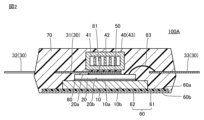
- FIG. 2 is a sectional view taken along line II-II in FIG.
- FIG. 2 shows a cross section of the semiconductor device 100A perpendicular to a first direction DR1, which will be described later.
- the semiconductor device 100A includes a heat spreader 10, a semiconductor element 20, a lead frame 30, a cooler 40, an insulating layer 50, an insulating sheet 60, and a sealing member 70. have.
- the heat spreader 10 has a first surface 10a and a second surface 10b.
- the first surface 10a and the second surface 10b are end surfaces of the heat spreader 10 in the thickness direction.
- the second surface 10b is the opposite surface to the first surface 10a.
- the heat spreader 10 is, for example, a copper plate.
- the heat spreader 10 is formed by, for example, a press molding method.
- the surface of the heat spreader 10 may have dimple-shaped or other unevenness formed thereon. This improves the adhesion with the sealing member 70 and suppresses peeling of the sealing member 70 from the heat spreader 10 due to thermal stress caused by heat generation during operation of the semiconductor device 100A.
- the semiconductor element 20 has a third surface 20a and a fourth surface 20b.
- the third surface 20a and the fourth surface 20b are end surfaces of the semiconductor element 20 in the thickness direction.
- the fourth surface 20b is the opposite surface to the third surface 20a.
- the semiconductor element 20 is, for example, an IGBT (Insulated Gate Bipolar Transistor).
- the semiconductor element 20 has a first electrode and a second electrode on the third surface 20a, and a third electrode on the fourth surface 20b.
- the first electrode and the second electrode are an emitter electrode and a gate electrode, respectively, and the third electrode is a collector electrode.
- the first electrode, the second electrode, and the third electrode are made of, for example, aluminum or an aluminum alloy containing silicon.
- the semiconductor element 20 is formed using a semiconductor substrate.
- the semiconductor substrate is made of a semiconductor material such as silicon, silicon carbide, gallium nitride, or diamond.
- the semiconductor element 20 is used, for example, in an inverter section that converts DC power into AC power.
- the semiconductor element 20 is placed on the heat spreader 10. More specifically, the semiconductor element 20 is arranged such that the fourth surface 20b faces the first surface 10a. The fourth surface 20b is electrically connected to the first surface 10a by a bonding material 80. Thereby, the third electrode of the semiconductor element 20 is electrically connected to the heat spreader 10.
- the bonding material 80 is made of, for example, a solder alloy or sintered silver particles.
- the lead frame 30 has a lead part 31, a lead part 32, and a plurality of lead parts 33.
- the lead frame 30 is formed, for example, by press-molding a copper plate.
- the surface of the lead frame 30 may have dimple-shaped unevenness formed thereon. This improves the adhesion with the sealing member 70 and suppresses peeling of the sealing member 70 from the lead frame 30 due to thermal stress caused by heat generation during operation of the semiconductor device 100A.
- the thickness of the lead frame 30 is preferably smaller than the thickness of the heat spreader 10.
- the lead portion 31 is electrically connected to the semiconductor element 20. More specifically, the lead portion 31 is electrically connected to the first electrode of the semiconductor element 20 by a bonding material 81.
- the bonding material 81 is made of, for example, a solder alloy or sintered silver particles.
- the lead portion 32 is electrically connected to the heat spreader 10. More specifically, the lead portion 32 is electrically connected to the first surface 10a by a bonding material 82 (not shown).
- the bonding material 82 is made of, for example, a solder alloy or sintered silver particles.
- the lead portion 33 is electrically connected to the semiconductor element 20. More specifically, the lead portion 33 is electrically connected to the second electrode of the semiconductor element 20 by wire bonding using a wire 83.
- the wire 83 is made of, for example, copper, iron, nickel, cobalt, aluminum, or an alloy thereof.
- a flow path 41 is provided inside the cooler 40.
- a refrigerant flows through the flow path 41 .
- the refrigerant is, for example, water, but is not limited to this.
- Fins 42 are provided inside the cooler 40 to improve cooling efficiency. Instead of the fins 42, pins may be provided inside the cooler 40.
- the cooler 40 is made of aluminum, copper, or the like, for example.
- the cooler 40 has a main body portion 43, a connecting portion 44, and a connecting portion 45.
- the main body portion 43 is arranged to face the third surface 20a with a space therebetween.
- the refrigerant flows inside the flow path 41 in the main body portion 43 along the first direction DR1.
- a plan view refers to a case where the semiconductor device 100A is viewed from a direction perpendicular to the third surface 20a.
- the connecting portion 44 is connected to one end of the main body portion 43 in the first direction DR1.
- the connecting portion 45 is connected to the other end of the main body portion 43 in the first direction DR1.
- the connecting portion 44 and the connecting portion 45 extend along the first direction DR1 in plan view.
- a hose is connected to the connecting portion 44 and the connecting portion 45.
- a refrigerant is supplied from a hose connected to the connection part 44. This refrigerant passes through the flow path 41 in the connection part 44 and flows in the flow path 41 in the main body part 43. and is discharged from the hose.
- the projected area of the cooler 40 is less than or equal to the projected area of the heat spreader 10.
- the width of the cooler 40 (main body portion 43) is preferably equal to or less than the width of the heat spreader 10.
- the insulating layer 50 is interposed between the third surface 20a and the cooler 40. More specifically, the insulating layer 50 is interposed between the cooler 40 and the third surface 20a to which the lead frame 30 (lead portion 31) is connected. The insulating layer 50 electrically insulates the cooler 40 and the semiconductor element 20 (lead frame 30).
- the insulating layer 50 is made of, for example, thermosetting resin such as epoxy resin. This thermosetting resin may contain filler. This filler is made of, for example, silica, alumina, boron nitride, or the like.
- the insulating sheet 60 has a fifth surface 60a and a sixth surface 60b.
- the fifth surface 60a and the sixth surface 60b are end surfaces of the insulating sheet 60 in the thickness direction.
- the sixth surface 60b is the opposite surface to the fifth surface 60a.
- the insulating sheet 60 has a metal layer 61 and an insulating layer 62.
- the metal layer 61 and the insulating layer 62 are overlapped.
- the fifth surface 60a is composed of an insulating layer 62
- the sixth surface 60b is composed of a metal layer 61.
- the metal layer 61 is, for example, a copper foil, a copper plate, an aluminum plate, or the like.
- the insulating layer 62 is made of, for example, thermosetting resin such as epoxy resin.
- thermosetting resin may contain filler.
- This filler is made of, for example, silica, alumina, boron nitride, or the like.
- the heat spreader 10 is arranged on the insulating sheet 60 so that the second surface 10b faces the fifth surface 60a.
- the sealing member 70 seals the heat spreader 10, the semiconductor element 20, the lead frame 30, the cooler 40, the insulating layer 50, and the insulating sheet 60.
- the metal layer 61 is exposed from the sealing member 70.
- the lead portion 31, the lead portion 32, and the lead portion 33 protrude from the outer peripheral edge of the sealing member 70 along the second direction DR2.
- the second direction DR2 is a direction orthogonal to the first direction DR1 in plan view.
- the connecting portion 44 and the connecting portion 45 protrude from the outer peripheral edge of the sealing member 70 along the first direction DR1.
- the lead portion 31, lead portion 32, and lead portion 33 that protrude from the outer periphery of the sealing member 70 in a plan view are connected to the connecting portion 44 and the connection portion that protrude from the outer periphery of the sealing member 70 in a plan view. It does not overlap with any of the 45.
- the sealing member 70 is made of, for example, thermosetting resin.
- This thermosetting resin is, for example, an epoxy resin or a phenol resin.
- the sealing member 70 is formed by, for example, transfer molding or compression molding. The sealing member 70 ensures electrical insulation between the sealed members and functions as a case of the semiconductor device 100A.
- an IGBT is used as an example of the semiconductor element 20, but the semiconductor element 20 may be a bipolar transistor, a MOSFET (Metal Oxide Semiconductor Field Effect Transistor), or a GTO (Gate Turn-Off thyristor). Further, the semiconductor element 20 may be a diode. Note that when the semiconductor element 20 is a diode, the semiconductor element 20 is used, for example, in a converter section that converts AC power into DC power.
- FIG. 3 is a plan view of a semiconductor device 100A according to a modification.
- the cooler 40 is shown in dotted lines.
- the semiconductor device 100A may include a plurality of semiconductor devices 100A.
- the lead portion 31 is electrically connected to the first electrode of each of the plurality of semiconductor elements 20.
- Method for manufacturing semiconductor device 100A A method of manufacturing the semiconductor device 100A will be described below.
- FIG. 4 is a manufacturing process diagram of the semiconductor device 100A. As shown in FIG. 4, the method for manufacturing the semiconductor device 100A includes a preparation step S1 and a sealing step S2.
- the heat spreader 10, the semiconductor element 20, the lead frame 30, the cooler 40, the insulating layer 50, and the insulating sheet 60 are prepared.
- the semiconductor element 20 is connected to the heat spreader 10 with the bonding material 80
- the lead part 31 is connected to the semiconductor element 20 with the bonding material 81
- the lead part 32 is connected to the heat spreader 10 with the bonding material 82.
- the lead portion 33 is connected to the semiconductor element 20 by a wire 83.
- an insulating layer 50 is interposed between the third surface 20a and the cooler 40, and an insulating sheet 60 (insulating layer 62) is attached to the second surface 10b.
- the sealing step S2 is performed after the preparation step S1.
- the heat spreader 10, the semiconductor element 20, the lead frame 30, the cooler 40, the insulating layer 50, and the insulating sheet 60 prepared in the preparatory step S1 are placed inside a mold.
- the upper mold presses down the parts of the lead part 31, lead part 32, lead part 33, connection part 44, and connection part 45 that protrude from the sealing member 70 after the sealing step S2.
- an uncured sealing member 70 is injected into the space between the upper mold and the lower mold. Note that due to the pressure when injecting the sealing member 70, the insulating layer 50 comes into close contact with the semiconductor element 20 and the cooler 40, and the insulating layer 62 comes into close contact with the metal layer 61 and the heat spreader 10.
- the sealing member 70 is heated. Thereby, the sealing member 70 is cured. Moreover, the insulating layer 50 and the insulating layer 62 are also hardened by this heating, and the semiconductor element 20 and the cooler 40 are bonded together with the insulating layer 50, and the metal layer 61 and the heat spreader 10 are bonded with the insulating layer 62. Through the above steps, the semiconductor device 100A having the structure shown in FIGS. 1 and 2 is manufactured.
- the projected area of the cooler 40 is less than or equal to the projected area of the heat spreader 10 in a plan view, and therefore miniaturization is possible. Note that when the width of the cooler 40 (main body portion 43) in the first direction DR1 is equal to or less than the width of the heat spreader 10, further miniaturization is possible.
- the cooler 40 cools the semiconductor element 20 without diffusing the heat generated in the semiconductor element 20.
- the lead frame 30 (lead portion 31) and the insulating layer 50 are present between the cooler 40 and the semiconductor element 20, these members are not intended to diffuse the heat generated in the semiconductor element 20. Therefore, even if the projected area of the cooler 40 is smaller than the projected area of the heat spreader 10 in plan view, the cooling capacity is unlikely to decrease. In this way, the semiconductor device 100A can achieve both high cooling capacity and miniaturization.
- the extending directions of the lead parts 31 , 32 , and 33 that protrude from the outer periphery of the sealing member 70 are the extension directions of the connecting parts 44 and 45 that protrude from the outer periphery of the sealing member 70 .
- the directions are orthogonal, it is possible to simplify the shapes of the upper mold and the lower mold, and it is possible to suppress damage and chipping of the semiconductor device 100A and the mold during die cutting.
- Embodiment 2 A semiconductor device according to a second embodiment will be described.
- the semiconductor device according to the second embodiment is referred to as a semiconductor device 100B.
- differences from the semiconductor device 100A will be mainly explained, and duplicate explanations will not be repeated.
- FIG. 5 is a cross-sectional view of the semiconductor device 100B.
- FIG. 5 shows a cross section of the semiconductor device 100B at a position corresponding to II-II in FIG.
- the semiconductor device 100B includes a heat spreader 10, a semiconductor element 20, a lead frame 30, a cooler 40, an insulating layer 50, an insulating sheet 60, and a sealing member 70. have.
- the semiconductor device 100B further includes a bonding material 80, a bonding material 81, a bonding material 82 (not shown), and a wire 83. Regarding these points, the configuration of the semiconductor device 100B is common to the configuration of the semiconductor device 100A.
- the sealing member 70 is filled between the third surface 20a and the cooler 40 (between the lead part 31 and the cooler 40), and the sealing member 70 is filled between the third surface 20a and the cooler 40.
- the portion of the sealing member 70 filled in the insulating layer 50 functions as the insulating layer 50.
- the configuration of the semiconductor device 100B is different from the configuration of the semiconductor device 100A.
- Method for manufacturing semiconductor device 100B A method for manufacturing the semiconductor device 100B will be described below.
- the method for manufacturing the semiconductor device 100B includes a preparation step S1 and a sealing step S2.
- the method for manufacturing the semiconductor device 100B is common to the method for manufacturing the semiconductor device 100A.
- the insulating layer 50 is not interposed between the semiconductor element 20 and the cooler 40 in the preparation step S1. Furthermore, in the method for manufacturing the semiconductor device 100B, when the heat spreader 10, the semiconductor element 20, the lead frame 30, the cooler 40, and the insulating sheet 60 are placed inside the mold, there is a gap between the semiconductor element 20 and the cooler 40. The space is empty. The sealing member 70 injected into the mold will flow into this space. Regarding these points, the method for manufacturing the semiconductor device 100B is different from the method for manufacturing the semiconductor device 100A.
- the sealing member 70 since a part of the sealing member 70 can function as the insulating layer 50, it is not necessary to provide the insulating layer 50 separately from the sealing member 70, and the number of members used can be reduced. Can be done.
- the adhesion between the semiconductor element 20 and the cooler 40 will be insufficient. Sometimes. In the semiconductor device 100B, since a part of the sealing member 70 functions as the insulating layer 50, a decrease in adhesion between the semiconductor element 20 and the cooler 40 due to the insulating layer 50 not being cured at an appropriate timing is suppressed. It is possible.
- Embodiment 3 A semiconductor device according to a third embodiment will be described.
- the semiconductor device according to the third embodiment is referred to as a semiconductor device 100C.
- differences from the semiconductor device 100A will be mainly explained, and duplicate explanations will not be repeated.
- FIG. 6 is a cross-sectional view of the semiconductor device 100C.
- FIG. 6 shows a cross section of the semiconductor device 100C at a position corresponding to II-II in FIG.
- the semiconductor device 100B includes a heat spreader 10, a semiconductor element 20, a lead frame 30, a cooler 40, an insulating layer 50, and a sealing member 70.
- the semiconductor device 100C further includes a bonding material 80, a bonding material 81, a bonding material 82 (not shown), and a wire 83. Regarding these points, the configuration of the semiconductor device 100C is common to the configuration of the semiconductor device 100A.
- the semiconductor device 100C has an insulating substrate 63 instead of the insulating sheet 60.
- the insulating substrate 63 includes an insulating base material 64, a conductive layer 65, and a conductive layer 66.
- the insulating base material 64 has a seventh surface 64a and an eighth surface 64b.
- the seventh surface 64a and the eighth surface 64b are end surfaces of the insulating base material 64 in the thickness direction.
- the eighth surface 64b is the opposite surface to the seventh surface 64a.
- the insulating base material 64 is made of, for example, a ceramic material such as alumina, aluminum nitride, silicon nitride, or the like.
- the thickness of the insulating base material 64 is appropriately selected from the viewpoint of ensuring the necessary dielectric strength voltage.
- the conductive layer 65 is arranged on the seventh surface 64a.
- the conductive layer 66 is arranged on the eighth surface 64b.
- the conductive layer 65 and the conductive layer 66 are made of copper, aluminum, etc., for example.
- the semiconductor element 20 is arranged such that the fourth surface 20b faces the conductive layer 65.
- the fourth surface 20b and the conductive layer 65 are electrically connected by the bonding material 80, and the conductive layer 65 and the lead part 32 are electrically connected by the bonding material 82. That is, in the semiconductor device 100C, the conductive layer 65 functions as the heat spreader 10.
- the thickness of the conductive layer 65 and the thickness of the conductive layer 66 are appropriately selected from the viewpoint of ensuring cooling capacity. From the viewpoint of suppressing warpage of the insulating substrate 63, the thickness of the conductive layer 65 and the thickness of the conductive layer 66 are preferably equal.
- the projected area of the cooler 40 is less than or equal to the projected area of the heat spreader 10 in plan view, so it is possible to achieve both high cooling capacity and miniaturization.
- Embodiment 4 A semiconductor device according to a fourth embodiment will be described.
- the semiconductor device according to the fourth embodiment is referred to as a semiconductor device 100D.
- differences from the semiconductor device 100A will be mainly explained, and duplicate explanations will not be repeated.
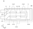
- FIG. 7 is a plan view of the semiconductor device 100D.
- the semiconductor device 100D includes a heat spreader 10, a semiconductor element 20, a lead frame 30, a cooler 40, an insulating layer 50, an insulating sheet 60, and a sealing member 70. ing.
- the semiconductor device 100D further includes a bonding material 80, a bonding material 81, and a bonding material 82 (not shown). Regarding these points, the configuration of the semiconductor device 100D is common to the configuration of the semiconductor device 100A.
- the semiconductor device 100D has a plurality of semiconductor elements 20. More specifically, the semiconductor device 100D includes a semiconductor element 20A and a semiconductor element 20B. The semiconductor element 20A and the semiconductor element 20B are lined up along the second direction DR2 in plan view.
- the lead portion 31 is electrically connected to the third surface 20a of the semiconductor element 20A and the third surface 20a of the semiconductor element 20B by a bonding material 81.
- the cooler 40 includes a main body portion 46a, a main body portion 46b, and a connecting portion 47a, a connecting portion 47b, and a connecting portion 47c.
- the main body portion 46a and the main body portion 46b are arranged to face the third surface 20a of the semiconductor element 20A and the third surface 20a of the semiconductor element 20B, respectively, with an insulating layer 50 interposed therebetween.
- the connecting portion 47a is connected to one end of the main body portion 46a in the first direction DR1.
- the connecting portion 47b is connected to one end of the main body portion 46b in the first direction DR1.
- the connecting portion 47a and the connecting portion 47b protrude from only one side of the outer peripheral edge of the sealing member 70 in plan view along the first direction DR1.
- the connecting portion 47c connects the other end of the main body portion 46a in the first direction DR1 and the other end of the main body portion 46b in the first direction DR1.
- the connecting portion 47c is not exposed from the sealing member 70.
- the configuration of the semiconductor device 100D is different from the configuration of the semiconductor device 100A.
- the semiconductor device 100D even when the semiconductor element 20 is located at an uneven position, it is possible to achieve both high cooling capacity and miniaturization.
- the semiconductor device 100D since the connecting portion 47a and the connecting portion 47b protrude from only one side of the outer peripheral edge of the sealing member 70 in a plan view, the semiconductor device 100D is Even when there are obstacles around, the semiconductor device 100D can be placed close to the obstacles, and the device in which the semiconductor device 100D is installed can be downsized.
- Embodiment 5 A semiconductor device according to a fifth embodiment will be described.
- the semiconductor device according to the fifth embodiment is referred to as a semiconductor device 100E.
- differences from the semiconductor device 100D will be mainly explained, and duplicate explanations will not be repeated.
- FIG. 8 is a plan view of the semiconductor device 100E.
- the semiconductor device 100E includes a heat spreader 10, a plurality of semiconductor elements 20 (a semiconductor element 20A and a semiconductor element 20B), a lead frame 30, a cooler 40, an insulating layer 50, and an insulating sheet. 60 and a sealing member 70.
- the semiconductor device 100E further includes a bonding material 80, a bonding material 81, and a bonding material 82 (not shown). Regarding these points, the configuration of the semiconductor device 100E is common to the configuration of the semiconductor device 100D.
- the cooler 40 further includes a connecting portion 47d.
- the connecting portion 47d is connected to the connecting portion 47c.
- the connecting portion 47d protrudes from the outer peripheral edge of the sealing member 70 in a plan view along the first direction DR1.
- the side of the outer periphery of the sealing member 70 from which the connecting portion 47d protrudes is on the opposite side in the first direction DR1 from the side of the outer periphery of the sealing member 70 from which the connecting portion 47a and the connecting portion 47b protrude. That is, in the semiconductor device 100E, the number of connection parts of the cooler 40 protruding from the outer peripheral edge of the sealing member 70 in plan view is three.
- the refrigerant is supplied, for example, from a hose connected to the connection part 47d, and is branched off at the connection part between the flow path 41 in the connection part 47d and the flow path 41 in the connection part 47c.
- One of the branched refrigerants flows through the flow path 41 in the connection portion 47c, the flow path 41 in the main body portion 46a, and the flow path in the connection portion 47a, and is discharged from the hose connected to the connection portion 47a.
- the other branched refrigerant flows through the flow path 41 in the connection part 47c, the flow path 41 in the main body part 46b, and the flow path in the connection part 47b, and is discharged from the hose connected to the connection part 47a. Ru. Regarding these points, the configuration of the semiconductor device 100E is different from the configuration of the semiconductor device 100D.
- FIG. 9 is a plan view of a semiconductor device 100E according to a modification.
- the cooler 40 may include a connecting portion 47e and a connecting portion 47f instead of the connecting portion 47d.
- the connecting portion 47e and the connecting portion 47f are connected to the other end of the main body portion 46a in the first direction DR1 and the other end of the main body portion 46b in the first direction DR1, respectively.
- the connecting portion 47e and the connecting portion 47f protrude from the outer peripheral edge of the sealing member 70 in a plan view along the first direction DR1.
- the side of the outer periphery of the sealing member 70 from which the connecting portion 47e and the connecting portion 47f protrude is opposite in the first direction DR1 from the side of the outer periphery of the sealing member 70 from which the connecting portion 47a and the connecting portion 47b protrude. It's on the side. That is, in the semiconductor device 100E, the number of connection parts of the cooler 40 protruding from the outer peripheral edge of the sealing member 70 in plan view may be three or more.
- the cooler 40 When the cooler 40 has the connection part 47e and the connection part 47f, the refrigerant is supplied from the hose connected to the connection part 47e, and the refrigerant is supplied from the flow path 41 in the connection part 47e and the flow path in the main body part 46a. 41 and the flow path 41 in the connection part 47a, and is discharged from the hose connected to the connection part 47a.
- the refrigerant is supplied from the hose connected to the connection part 47f, flows through the flow path 41 in the connection part 47f, the flow path 41 in the main body part 46b, and the flow path 41 in the connection part 47b, and then flows into the connection part 47b. It is discharged from the connected hose.
- the cooler 40 may have a plurality of independent flow paths 41.
- the semiconductor device 100E it is possible to branch the flow path 41 of the cooler 40 midway or to provide a plurality of independent flow paths 41 in the cooler 40. Therefore, in the semiconductor device 100E, it is possible to further increase the cooling capacity while making it possible to downsize the semiconductor device 100E.
- Embodiment 6 the semiconductor device according to the first to fifth embodiments described above is applied to a power conversion device.
- the present disclosure is not limited to a specific power conversion device, a case will be described below as a sixth embodiment in which the present disclosure is applied to a three-phase inverter.
- the power conversion system according to the sixth embodiment is referred to as a power conversion system 200.
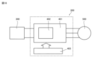
- FIG. 10 is a block diagram showing the configuration of the power conversion system 200.
- the power conversion system includes a power source 300, a power conversion device 400, and a load 500.
- Power supply 300 is a DC power supply and supplies DC power to power conversion device 400.
- the power source 300 can be composed of various things, for example, it can be composed of a DC system, a solar battery, a storage battery, or it can be composed of a rectifier circuit or an AC/DC converter connected to an AC system. Good too.
- the power supply 300 may be configured with a DC/DC converter that converts DC power output from a DC system into predetermined power.
- the power conversion device 400 is a three-phase inverter connected between the power source 300 and the load 500, converts the DC power supplied from the power source 300 into AC power, and supplies the AC power to the load 500. As shown in FIG. 10, the power conversion device 400 includes a main conversion circuit 401 that converts DC power into AC power and outputs it, and a control circuit that outputs a control signal for controlling the main conversion circuit 401 to the main conversion circuit 401. 403.
- the load 500 is a three-phase electric motor driven by AC power supplied from the power converter 400.
- the load 500 is not limited to a specific application, but is a motor installed in various electrical devices, and is used, for example, as a motor for a hybrid vehicle, an electric vehicle, a railway vehicle, an elevator, or an air conditioner.
- the main conversion circuit 401 includes a switching element and a freewheeling diode (not shown), and when the switching element switches, it converts the DC power supplied from the power supply 300 into AC power, and supplies the AC power to the load 500.
- the main conversion circuit 401 is a two-level three-phase full bridge circuit, and includes six switching elements and each switching element. It can be composed of six freewheeling diodes connected in antiparallel to each other.
- each switching element and each freewheeling diode of main conversion circuit 401 is a switching element or freewheeling diode included in semiconductor module 402 corresponding to the semiconductor device according to any one of the first to fifth embodiments described above. be.
- the six switching elements are connected in series every two switching elements to constitute upper and lower arms, and each upper and lower arm constitutes each phase (U phase, V phase, W phase) of the full bridge circuit.
- the output terminals of the upper and lower arms that is, the three output terminals of the main conversion circuit 401, are connected to the load 500.
- the main conversion circuit 401 includes a drive circuit (not shown) that drives each switching element, but the drive circuit may be built into the semiconductor module 402 or may include a drive circuit separately from the semiconductor module 402. It may be.
- the drive circuit generates a drive signal for driving the switching element of the main conversion circuit 401 and supplies it to the control electrode of the switching element of the main conversion circuit 401. Specifically, according to a control signal from a control circuit 403, which will be described later, a drive signal that turns the switching element on and a drive signal that turns the switching element off are output to the control electrode of each switching element.
- the drive signal When keeping the switching element in the on state, the drive signal is a voltage signal (on signal) that is greater than or equal to the threshold voltage of the switching element, and when the switching element is kept in the off state, the drive signal is a voltage signal that is less than or equal to the threshold voltage of the switching element. signal (off signal).
- the control circuit 403 controls the switching elements of the main conversion circuit 401 so that the desired power is supplied to the load 500. Specifically, based on the power to be supplied to the load 500, the time during which each switching element of the main conversion circuit 401 should be in the on state (on time) is calculated. For example, the main conversion circuit 401 can be controlled by PWM control that modulates the on-time of the switching element according to the voltage to be output. Then, a control command (control signal) is sent to the drive circuit included in the main conversion circuit 401 so that an on signal is output to the switching element that should be in the on state at each time, and an off signal is output to the switching element that should be in the off state. Output.
- the drive circuit outputs an on signal or an off signal as a drive signal to the control electrode of each switching element according to this control signal.
- the semiconductor device according to the first to fifth embodiments described above is applied as the semiconductor module 402 constituting the main conversion circuit 401, the generation of thermal stress around the semiconductor element 20 is suppressed. At the same time, it is possible to reduce the current density in the current path from the semiconductor element 20.
- the present disclosure is not limited to this and can be applied to various power conversion devices.
- a two-level power converter is used, but a three-level or multi-level power converter may be used, and when supplying power to a single-phase load, the present disclosure may be applied to a single-phase inverter. May be applied.
- the present disclosure can also be applied to a DC/DC converter or an AC/DC converter.
- the power conversion device to which the present disclosure is applied is not limited to cases where the above-mentioned load is an electric motor. It can also be used as a power conditioner for solar power generation systems, power storage systems, etc.
- 10 heat spreader 10a first surface, 10b second surface, 20, 20A, 20B semiconductor element, 20a third surface, 20b fourth surface, 30 lead frame, 31, 32, 33 lead part, 40 cooler, 41 flow path , 42 fin, 43 main body part, 44, 45 connection part, 46a, 46b main body part, 47a, 47b, 47c, 47d, 47e, 47f connection part, 50 insulating layer, 60 insulating sheet, 60a fifth surface, 60b sixth Surface, 61 Metal layer, 62 Insulating layer, 63 Insulating substrate, 64 Insulating base material, 64a Seventh surface, 64b Eighth surface, 65, 66 Conductive layer, 70 Sealing member, 80, 81, 82 Bonding material, 83 Wire , 100A, 100B, 100C, 100D, 100E semiconductor device, 200 power conversion system, 300 power supply, 400 power conversion device, 401 main conversion circuit, 402 semiconductor module, 403 control circuit, 500 load, DR1 first direction, DR2 second Direction, S1 preparation process, S2 sealing process.
Landscapes
- Cooling Or The Like Of Semiconductors Or Solid State Devices (AREA)
- Cooling Or The Like Of Electrical Apparatus (AREA)
- Engineering & Computer Science (AREA)
- Microelectronics & Electronic Packaging (AREA)
Priority Applications (5)
| Application Number | Priority Date | Filing Date | Title |
|---|---|---|---|
| CN202280097137.6A CN119365978A (zh) | 2022-06-28 | 2022-06-28 | 半导体装置以及电力变换装置 |
| JP2023560654A JP7493686B1 (ja) | 2022-06-28 | 2022-06-28 | 半導体装置及び電力変換装置 |
| DE112022007435.3T DE112022007435T5 (de) | 2022-06-28 | 2022-06-28 | Halbleitervorrichtung und leistungsumwandlungsvorrichtung |
| US18/867,811 US20250364368A1 (en) | 2022-06-28 | 2022-06-28 | Semiconductor device and power conversion device |
| PCT/JP2022/025735 WO2024004026A1 (ja) | 2022-06-28 | 2022-06-28 | 半導体装置及び電力変換装置 |
Applications Claiming Priority (1)
| Application Number | Priority Date | Filing Date | Title |
|---|---|---|---|
| PCT/JP2022/025735 WO2024004026A1 (ja) | 2022-06-28 | 2022-06-28 | 半導体装置及び電力変換装置 |
Publications (1)
| Publication Number | Publication Date |
|---|---|
| WO2024004026A1 true WO2024004026A1 (ja) | 2024-01-04 |
Family
ID=89382139
Family Applications (1)
| Application Number | Title | Priority Date | Filing Date |
|---|---|---|---|
| PCT/JP2022/025735 Ceased WO2024004026A1 (ja) | 2022-06-28 | 2022-06-28 | 半導体装置及び電力変換装置 |
Country Status (5)
| Country | Link |
|---|---|
| US (1) | US20250364368A1 (https=) |
| JP (1) | JP7493686B1 (https=) |
| CN (1) | CN119365978A (https=) |
| DE (1) | DE112022007435T5 (https=) |
| WO (1) | WO2024004026A1 (https=) |
Cited By (2)
| Publication number | Priority date | Publication date | Assignee | Title |
|---|---|---|---|---|
| US20240321698A1 (en) * | 2023-03-23 | 2024-09-26 | Toyota Motor Engineering & Manufacturing North America, Inc. | Chip-on-chip power card having immersion cooling |
| WO2025243727A1 (ja) * | 2024-05-22 | 2025-11-27 | 三菱電機株式会社 | 電力半導体装置、及び、電力変換装置 |
Citations (7)
| Publication number | Priority date | Publication date | Assignee | Title |
|---|---|---|---|---|
| JPH02202043A (ja) * | 1989-01-31 | 1990-08-10 | Nec Corp | 樹脂封止型半導体装置 |
| JPH0427147A (ja) * | 1990-05-22 | 1992-01-30 | Seiko Epson Corp | 半導体装置 |
| JPH04254359A (ja) * | 1991-02-06 | 1992-09-09 | Toshiba Corp | 樹脂封止型半導体装置および半導体装置の実装構造 |
| US20060038284A1 (en) * | 2004-08-17 | 2006-02-23 | Brandenburg Scott D | Fluid cooled encapsulated microelectronic package |
| JP2012079950A (ja) * | 2010-10-04 | 2012-04-19 | Toyota Motor Corp | 半導体冷却装置 |
| JP2012164697A (ja) * | 2011-02-03 | 2012-08-30 | Mitsubishi Electric Corp | 電力用パワーモジュール及び電力用半導体装置 |
| JP2020053611A (ja) * | 2018-09-28 | 2020-04-02 | 三菱電機株式会社 | 半導体モジュール、および、半導体モジュールの製造方法 |
-
2022
- 2022-06-28 JP JP2023560654A patent/JP7493686B1/ja active Active
- 2022-06-28 WO PCT/JP2022/025735 patent/WO2024004026A1/ja not_active Ceased
- 2022-06-28 CN CN202280097137.6A patent/CN119365978A/zh active Pending
- 2022-06-28 US US18/867,811 patent/US20250364368A1/en active Pending
- 2022-06-28 DE DE112022007435.3T patent/DE112022007435T5/de not_active Withdrawn
Patent Citations (7)
| Publication number | Priority date | Publication date | Assignee | Title |
|---|---|---|---|---|
| JPH02202043A (ja) * | 1989-01-31 | 1990-08-10 | Nec Corp | 樹脂封止型半導体装置 |
| JPH0427147A (ja) * | 1990-05-22 | 1992-01-30 | Seiko Epson Corp | 半導体装置 |
| JPH04254359A (ja) * | 1991-02-06 | 1992-09-09 | Toshiba Corp | 樹脂封止型半導体装置および半導体装置の実装構造 |
| US20060038284A1 (en) * | 2004-08-17 | 2006-02-23 | Brandenburg Scott D | Fluid cooled encapsulated microelectronic package |
| JP2012079950A (ja) * | 2010-10-04 | 2012-04-19 | Toyota Motor Corp | 半導体冷却装置 |
| JP2012164697A (ja) * | 2011-02-03 | 2012-08-30 | Mitsubishi Electric Corp | 電力用パワーモジュール及び電力用半導体装置 |
| JP2020053611A (ja) * | 2018-09-28 | 2020-04-02 | 三菱電機株式会社 | 半導体モジュール、および、半導体モジュールの製造方法 |
Cited By (2)
| Publication number | Priority date | Publication date | Assignee | Title |
|---|---|---|---|---|
| US20240321698A1 (en) * | 2023-03-23 | 2024-09-26 | Toyota Motor Engineering & Manufacturing North America, Inc. | Chip-on-chip power card having immersion cooling |
| WO2025243727A1 (ja) * | 2024-05-22 | 2025-11-27 | 三菱電機株式会社 | 電力半導体装置、及び、電力変換装置 |
Also Published As
| Publication number | Publication date |
|---|---|
| JPWO2024004026A1 (https=) | 2024-01-04 |
| JP7493686B1 (ja) | 2024-05-31 |
| DE112022007435T5 (de) | 2025-04-10 |
| US20250364368A1 (en) | 2025-11-27 |
| CN119365978A (zh) | 2025-01-24 |
Similar Documents
| Publication | Publication Date | Title |
|---|---|---|
| US12476190B2 (en) | Semiconductor device, power converter, method for manufacturing semiconductor device, and method for manufacturing power converter | |
| JP6752381B1 (ja) | 半導体モジュールおよび電力変換装置 | |
| CN112701093A (zh) | 半导体模块及电力转换装置 | |
| JP7561677B2 (ja) | 電力半導体装置、電力半導体装置の製造方法及び電力変換装置 | |
| US11908822B2 (en) | Power semiconductor module and power conversion apparatus | |
| JP6575739B1 (ja) | 半導体装置、半導体装置の製造方法および電力変換装置 | |
| US20240395678A1 (en) | Semiconductor device, method of manufacturing semiconductor device, and power conversion device | |
| JP7493686B1 (ja) | 半導体装置及び電力変換装置 | |
| CN111052325B (zh) | 半导体模块以及电力转换装置 | |
| JP7019024B2 (ja) | 半導体装置及び電力変換装置 | |
| JP2018147958A (ja) | 半導体パワーモジュール及び電力変換装置 | |
| JP7693094B2 (ja) | パワーモジュール半導体パッケージおよび半導体装置 | |
| JP2024138858A (ja) | 電力用半導体装置、電力変換装置、及び、電力用半導体装置の製造方法 | |
| CN116031226A (zh) | 半导体装置及电力转换装置 | |
| JP7851410B2 (ja) | 半導体装置、電力変換装置および半導体装置の製造方法 | |
| JP6885522B1 (ja) | 半導体装置、電力変換装置および半導体装置の製造方法 | |
| US20260047450A1 (en) | Semiconductor device and method for manufacturing semiconductor device | |
| JP7308788B2 (ja) | 半導体装置の製造方法、および、電力変換装置の製造方法 | |
| US20240274557A1 (en) | Semiconductor device and power converting device | |
| WO2025017833A1 (ja) | 半導体装置、電力変換装置、個片パッケージ、及び個片パッケージの製造方法 | |
| JP2026058632A (ja) | 電力用半導体装置および電力変換装置 |
Legal Events
| Date | Code | Title | Description |
|---|---|---|---|
| ENP | Entry into the national phase |
Ref document number: 2023560654 Country of ref document: JP Kind code of ref document: A |
|
| 121 | Ep: the epo has been informed by wipo that ep was designated in this application |
Ref document number: 22949303 Country of ref document: EP Kind code of ref document: A1 |
|
| WWE | Wipo information: entry into national phase |
Ref document number: 18867811 Country of ref document: US |
|
| WWE | Wipo information: entry into national phase |
Ref document number: 202280097137.6 Country of ref document: CN |
|
| WWP | Wipo information: published in national office |
Ref document number: 202280097137.6 Country of ref document: CN |
|
| WWE | Wipo information: entry into national phase |
Ref document number: 112022007435 Country of ref document: DE |
|
| WWP | Wipo information: published in national office |
Ref document number: 112022007435 Country of ref document: DE |
|
| 122 | Ep: pct application non-entry in european phase |
Ref document number: 22949303 Country of ref document: EP Kind code of ref document: A1 |
|
| WWP | Wipo information: published in national office |
Ref document number: 18867811 Country of ref document: US |