WO2023286459A1 - 信号生成回路、スイッチング装置及びスイッチング電源装置 - Google Patents
信号生成回路、スイッチング装置及びスイッチング電源装置 Download PDFInfo
- Publication number
- WO2023286459A1 WO2023286459A1 PCT/JP2022/021398 JP2022021398W WO2023286459A1 WO 2023286459 A1 WO2023286459 A1 WO 2023286459A1 JP 2022021398 W JP2022021398 W JP 2022021398W WO 2023286459 A1 WO2023286459 A1 WO 2023286459A1
- Authority
- WO
- WIPO (PCT)
- Prior art keywords
- signal
- voltage
- reference voltage
- ramp
- switching
- Prior art date
- Legal status (The legal status is an assumption and is not a legal conclusion. Google has not performed a legal analysis and makes no representation as to the accuracy of the status listed.)
- Ceased
Links
Images












Classifications
-
- H—ELECTRICITY
- H02—GENERATION; CONVERSION OR DISTRIBUTION OF ELECTRIC POWER
- H02M—APPARATUS FOR CONVERSION BETWEEN AC AND AC, BETWEEN AC AND DC, OR BETWEEN DC AND DC, AND FOR USE WITH MAINS OR SIMILAR POWER SUPPLY SYSTEMS; CONVERSION OF DC OR AC INPUT POWER INTO SURGE OUTPUT POWER; CONTROL OR REGULATION THEREOF
- H02M1/00—Details of apparatus for conversion
- H02M1/0003—Details of control, feedback or regulation circuits
- H02M1/0025—Arrangements for modifying reference values, feedback values or error values in the control loop of a converter
-
- H—ELECTRICITY
- H02—GENERATION; CONVERSION OR DISTRIBUTION OF ELECTRIC POWER
- H02M—APPARATUS FOR CONVERSION BETWEEN AC AND AC, BETWEEN AC AND DC, OR BETWEEN DC AND DC, AND FOR USE WITH MAINS OR SIMILAR POWER SUPPLY SYSTEMS; CONVERSION OF DC OR AC INPUT POWER INTO SURGE OUTPUT POWER; CONTROL OR REGULATION THEREOF
- H02M1/00—Details of apparatus for conversion
- H02M1/44—Circuits or arrangements for compensating for electromagnetic interference in converters or inverters
-
- H—ELECTRICITY
- H02—GENERATION; CONVERSION OR DISTRIBUTION OF ELECTRIC POWER
- H02M—APPARATUS FOR CONVERSION BETWEEN AC AND AC, BETWEEN AC AND DC, OR BETWEEN DC AND DC, AND FOR USE WITH MAINS OR SIMILAR POWER SUPPLY SYSTEMS; CONVERSION OF DC OR AC INPUT POWER INTO SURGE OUTPUT POWER; CONTROL OR REGULATION THEREOF
- H02M3/00—Conversion of DC power input into DC power output
- H02M3/02—Conversion of DC power input into DC power output without intermediate conversion into AC
- H02M3/04—Conversion of DC power input into DC power output without intermediate conversion into AC by static converters
- H02M3/10—Conversion of DC power input into DC power output without intermediate conversion into AC by static converters using discharge tubes with control electrode or semiconductor devices with control electrode
- H02M3/145—Conversion of DC power input into DC power output without intermediate conversion into AC by static converters using discharge tubes with control electrode or semiconductor devices with control electrode using devices of a triode or transistor type requiring continuous application of a control signal
- H02M3/155—Conversion of DC power input into DC power output without intermediate conversion into AC by static converters using discharge tubes with control electrode or semiconductor devices with control electrode using devices of a triode or transistor type requiring continuous application of a control signal using semiconductor devices only
- H02M3/156—Conversion of DC power input into DC power output without intermediate conversion into AC by static converters using discharge tubes with control electrode or semiconductor devices with control electrode using devices of a triode or transistor type requiring continuous application of a control signal using semiconductor devices only with automatic control of output voltage or current, e.g. switching regulators
- H02M3/158—Conversion of DC power input into DC power output without intermediate conversion into AC by static converters using discharge tubes with control electrode or semiconductor devices with control electrode using devices of a triode or transistor type requiring continuous application of a control signal using semiconductor devices only with automatic control of output voltage or current, e.g. switching regulators including plural semiconductor devices as final control devices for a single load
-
- H—ELECTRICITY
- H03—ELECTRONIC CIRCUITRY
- H03K—PULSE TECHNIQUE
- H03K4/00—Generating pulses having essentially a finite slope or stepped portions
- H03K4/06—Generating pulses having essentially a finite slope or stepped portions having triangular shape
Definitions
- the present disclosure relates to signal generation circuits, switching devices, and switching power supplies.
- Spread spectrum technology is a technology that suppresses the effects of noise.
- Spread-spectrum techniques spread the noise over a wide band, making it possible to suppress the effects of substantial noise.
- An object of the present disclosure is to provide a signal generation circuit, a switching device, and a switching power supply that contribute to reducing the influence of noise.
- a signal generation circuit includes a reference voltage generation circuit configured to generate a reference voltage, a ramp voltage generation circuit configured to generate a ramp voltage that fluctuates within a predetermined voltage range, and the reference and a comparison circuit configured to output a comparison result signal representing the magnitude relationship between the voltage and the lamp voltage, wherein the reference voltage generation circuit causes the reference voltage to have a triangular waveform, and the triangular wave. Vary the frequency of
- FIG. 1 is a configuration diagram of a switching device according to the first embodiment of the present disclosure.
- FIG. 2 is a relationship diagram of multiple voltages and multiple signals in a first pattern according to the first embodiment of the present disclosure.
- FIG. 3 is a relationship diagram of multiple voltages and multiple signals in a second pattern according to the first embodiment of the present disclosure.
- FIG. 4 is a diagram showing the time dependence of the reference voltage according to the first reference example.
- FIG. 5 is a diagram showing the time dependence of the frequency of the comparison result signal according to the first reference example.
- FIG. 6 is a diagram showing the frequency spectrum of the comparison result signal according to the first reference example.
- FIG. 7 is a relationship diagram of the reference voltage, the ramp voltage, and a plurality of signals in the process of increasing the reference voltage.
- FIG. 1 is a configuration diagram of a switching device according to the first embodiment of the present disclosure.
- FIG. 2 is a relationship diagram of multiple voltages and multiple signals in a first pattern according to the first embodiment of the present
- FIG. 8 is a relationship diagram of the reference voltage, the ramp voltage, and a plurality of signals in the process of decreasing the reference voltage.
- FIG. 9 is a diagram showing the time dependence of the reference voltage according to the second reference example.
- FIG. 10 is a diagram showing the time dependence of the frequency of the comparison result signal according to the second reference example.
- FIG. 11 is a diagram showing the frequency spectrum of the comparison result signal according to the second reference example.
- FIG. 12 is a diagram showing the time dependence of the reference voltage according to the third reference example.
- FIG. 13 is a diagram showing waveforms of reference voltages according to example EX1_A belonging to the first embodiment of the present disclosure.
- FIG. 14 is a diagram showing how the period of the triangular wave forming the reference voltage cyclically fluctuates according to the example EX1_A belonging to the first embodiment of the present disclosure.
- FIG. 15 is a diagram showing the time dependence of the reference voltage, according to example EX1_A belonging to the first embodiment of the present disclosure.
- FIG. 16 is a diagram showing the time dependence of the frequency of the comparison result signal, according to example EX1_A belonging to the first embodiment of the present disclosure.
- FIG. 17 is a diagram showing a frequency spectrum of a comparison result signal according to example EX1_A belonging to the first embodiment of the present disclosure.
- FIG. 18 is a diagram showing an internal configuration example of a reference voltage generation circuit according to example EX1_B belonging to the first embodiment of the present disclosure.
- FIG. 19 is a diagram showing a waveform example of an output signal of the rectangular wave supply circuit of FIG. 18, according to Example EX1_B belonging to the first embodiment of the present disclosure.
- FIG. 20 is a diagram showing an example of the relationship between the output signal of the rectangular wave supply circuit of FIG. 18 and the reference voltage, according to the example EX1_B belonging to the first embodiment of the present disclosure.
- FIG. 21 is a diagram showing an internal configuration example of the rectangular wave supply circuit of FIG.
- FIG. 22 is a diagram illustrating an internal configuration example of a reference voltage generating circuit according to example EX1_C belonging to the first embodiment of the present disclosure.
- FIG. 23 is a configuration diagram of a switching power supply device according to the second embodiment of the present disclosure.
- FIG. 24 is an external perspective view of a semiconductor device according to a second embodiment of the present disclosure.
- the ground refers to a reference conductive portion having a potential of 0 V (zero volt) as a reference, or refers to a potential of 0 V itself.
- the reference conductive portion is made of a conductor such as metal.
- a potential of 0 V is sometimes referred to as a ground potential.
- voltages shown without specific reference represent potentials with respect to ground.
- a level refers to a level of potential, and for any signal or voltage of interest, a high level has a higher potential than a low level.
- Any digital signal can have a high or low signal level.
- the signal or voltage of interest strictly speaking that the signal or voltage is at a high level means that the signal or voltage is at a high level, and strictly speaking that the signal or voltage is at a low level. It means that the signal or voltage level is at low level.
- Levels for signals are sometimes referred to as signal levels, and levels for voltages are sometimes referred to as voltage levels.
- the switching from low level to high level is called up edge (or rising edge), and the timing of switching from low level to high level is called up edge timing (or rising edge timing). .
- the switching from high level to low level is called the falling edge (or falling edge), and the timing of switching from high level to low level is called the falling edge timing (or falling edge). edge timing).
- the ON state refers to the state in which there is conduction between the drain and source of the transistor
- the OFF state refers to the state in which there is conduction between the drain and source of the transistor. It refers to the state in which the current between the two is non-conducting (blocking state).
- MOSFETs are understood to be enhancement mode MOSFETs unless otherwise stated.
- MOSFET is an abbreviation for "metal-oxide-semiconductor field-effect transistor".
- the on state and off state of any transistor may be simply expressed as on and off.
- switching from an off state to an on state is expressed as turn-on, and switching from an on state to an off state is expressed as turn-off.
- a period during which the transistor is on is sometimes referred to as an on period, and a period during which the transistor is off is sometimes referred to as an off period.
- a period during which the level of the signal is high is called a high level period
- a period during which the level of the signal is low is called a low level period.
- the same is true for any voltage that takes a high or low voltage level.
- Connections between multiple parts forming a circuit such as arbitrary circuit elements, wiring (lines), nodes, etc., mean electrical connections unless otherwise specified.
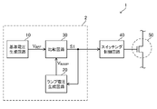
- FIG. 1 is a configuration diagram of a switching device 1 according to the first embodiment of the present disclosure.
- the switching device 1 includes a reference voltage generation circuit 10 , a ramp voltage generation circuit 20 , a comparison circuit 30 , a switching control circuit 40 and a switching transistor 50 .
- the switching device 1 contains a signal generation circuit 2 which can also be referred to as a spread spectrum signal generation circuit.
- the signal generation circuit 2 includes a reference voltage generation circuit 10 , a ramp voltage generation circuit 20 and a comparison circuit 30 .
- a reference voltage generation circuit 10 generates and outputs a reference voltage VREF .
- the reference voltage VREF has a triangular waveform, which will be discussed later.
- a ramp voltage generation circuit 20 generates and outputs a ramp voltage VRAMP that varies within a predetermined voltage range.
- the reference voltage V REF and the ramp voltage V RAMP are input to the comparison circuit 30 .
- the comparison circuit 30 compares the reference voltage VREF and the ramp voltage VRAMP , and generates and outputs a signal S1, which is a comparison result signal indicating the level relationship between the reference voltage VREF and the ramp voltage VRAMP .
- Signal S1 is input to switching control circuit 40 .
- the switching control circuit 40 switches the switching transistor 50 based on the signal S1.
- the switching of transistor 50 toggles the state of transistor 50 between an on state and an off state.
- the signal S1 is also input to the ramp voltage generation circuit 20.
- switching transistor 50 may be any type of transistor. That is, the switching transistor 50 may be either an N-channel MOSFET or a P-channel MOSFET. Also, the switching transistor 50 may be a bipolar transistor, a junction FET, or an IGBT (Insulated Gate Bipolar Transistor). In this embodiment, hereinafter, the switching transistor 50 is considered to be an N-channel MOSFET.
- the switching control circuit 40 can turn on or off the switching transistor 50 by controlling the gate potential of the switching transistor 50 (in other words, by controlling the gate-source voltage of the switching transistor 50). can.
- the signal S1 is a binary signal (digital signal) that takes a value of "0" or "1".
- the signal S1 takes either a low level or a high level, the low level signal S1 indicating a value of "0” and the high level signal S1 indicating a value of "1".
- a modification that applies negative logic to the signal S1 is also possible.
- the following first pattern or second pattern can be adopted.
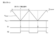
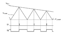
- FIG. 2 shows the relationship between the reference voltage VREF, the ramp voltage VRAMP , and the signal S1 in the first pattern.
- Signal S2 is also shown in FIG. 2 and will be discussed later.
- the reference voltage VREF has a triangular waveform, but the frequency of the reference voltage VREF (in other words, the frequency of the triangular wave in the reference voltage VREF ) is much higher than the frequency of the ramp voltage VRAMP . Because it is small, FIG. 2 shows each voltage waveform as if the value of the reference voltage VREF is constant (the same applies to FIG. 3, which will be described later).
- the comparison circuit 30 sets the signal S1 to a low level (that is, makes the signal S1 have a value of “0”) when the ramp voltage V RAMP is lower than the reference voltage V REF , and the ramp voltage V RAMP is When the voltage is higher than the reference voltage VREF , the signal S1 is set to a high level (that is, the signal S1 has a value of "1").
- the comparison circuit 30 changes from a state where the ramp voltage V RAMP is lower than the reference voltage V REF (that is, “V RAMP ⁇ V REF ”) to a state that is higher than the reference voltage V REF (that is, “ V RAMP >V REF "), an up edge is generated in the signal S1 (that is, the value of the signal S1 is changed from “0" to "1").
- V RAMP ⁇ V REF the reference voltage V REF
- the ramp voltage generation circuit 20 according to the first pattern generates the ramp voltage VRAMP shown in FIG. 2 by repeatedly executing the following first ramp unit operation.
- the ramp voltage generation circuit 20 starts from a state in which the ramp voltage V RAMP matches the predetermined lower limit voltage V L#RAMP , and increases the ramp voltage V RAMP from the lower limit voltage V L#RAMP by a predetermined amount.
- the ramp voltage generation circuit 20 ends the i-th first lamp unit operation.
- the (i+1)th first lamp unit operation is started.
- the increasing slope U #RAMP and the decreasing slope D #RAMP are constant.
- i represents any natural number.
- the magnitudes of the increasing slope U #RAMP and the decreasing slope D #RAMP may be the same.
- the repetition of the first ramp unit operation in the first pattern produces an up edge in signal S1 each time ramp voltage V RAMP reaches reference voltage V REF .
- the state of "V RAMP > V REF” quickly changes to the state of "V RAMP ⁇ V REF ".
- the length of the level period is minute. In other words, a down edge occurs in the signal S1 after a short period of time after the up edge of the signal S1.
- the lower limit voltage V L_RAMP is lower than the lower limit of the variation range of the reference voltage V REF (how the reference voltage V REF varies is not shown in FIG. 2). Therefore, in each of the repeatedly executed first ramp unit operations, an up edge always occurs in signal S1.
- the signal S2 shown in FIG. 2 may be generated based on the signal S1 and the ramp voltage VRAMP .
- the signal S2 like the signal S1, takes a signal level of low level or high level.
- an up edge occurs in the signal S2 in synchronism with the up edge of the signal S1, and then the ramp voltage V RAMP monotonously decreases, and the ramp voltage V RAMP drops to the lower limit voltage V L#RAMP . Triggered by this, a down edge occurs in the signal S2.
- FIG. 3 shows the relationship between the reference voltage VREF, the ramp voltage VRAMP , and the signal S1 in the second pattern.
- Signal S2 is also shown in FIG. 3 and will be described later.
- the comparison circuit 30 sets the signal S1 to a low level (that is, makes the signal S1 have a value of “0”) when the ramp voltage V RAMP is higher than the reference voltage V REF , and the ramp voltage V RAMP is When the voltage is lower than the reference voltage VREF , the signal S1 is set to a high level (that is, the signal S1 has a value of "1").
- the comparison circuit 30 changes from a state where the ramp voltage V RAMP is higher than the reference voltage V REF (that is, “V RAMP >V REF ”) to a state that is lower than the reference voltage V REF (that is, “ V RAMP ⁇ V REF ” state), an up edge is generated in the signal S1 (that is, the value of the signal S1 is changed from “0” to “1”).
- V RAMP the ramp voltage
- the ramp voltage generating circuit 20 generates the ramp voltage VRAMP shown in FIG. 3 by repeatedly executing the following second ramp unit operation.
- the ramp voltage generation circuit 20 starts from a state in which the ramp voltage V RAMP is made equal to the predetermined upper limit voltage V H #RAMP and decreases the ramp voltage V RAMP from the upper limit voltage V H#RAMP by a predetermined amount.
- the signal S1 has an up edge (when the value of the signal S1 changes from "0" to "1")
- the ramp voltage The change direction of V RAMP is reversed from the decreasing direction to the increasing direction, and thereafter the ramp voltage V RAMP is linearly and monotonically increased toward the upper limit voltage V H_RAMP at a predetermined increasing slope U #RAMP .
- the ramp voltage generating circuit 20 ends the i-th second lamp unit operation. Simultaneously, the (i+1)th second lamp unit operation is started.
- the repetition of the second ramp unit operation in the second pattern produces an up edge in signal S1 each time ramp voltage V RAMP falls to reference voltage V REF .
- the state of "V RAMP ⁇ V REF” quickly changes to the state of "V RAMP > V REF ".
- the length of the level period is minute. In other words, a down edge occurs in the signal S1 after a short period of time after the up edge of the signal S1.
- the upper limit voltage V H_RAMP is higher than the upper limit of the variation range of the reference voltage V REF (how the reference voltage V REF varies is not shown in FIG. 3). Therefore, an up edge always occurs in the signal S1 in each of the repetitively executed second ramp unit operations.
- the signal S2 shown in FIG. 3 may be generated based on the signal S1 and the ramp voltage VRAMP .
- the signal S2 like the signal S1, takes a signal level of low level or high level.
- an up edge occurs in the signal S2 in synchronization with the up edge of the signal S1, and then the ramp voltage V RAMP monotonically increases to reach the upper limit voltage V H#RAMP .
- a down edge occurs in the signal S2.
- the operation of the switching control circuit 40 is common between the first pattern and the second pattern described above.
- the switching control circuit 40 turns on or off the switching transistor 50 at the rising edge of the signal S1 (in other words, in synchronization with the rising edge of the signal S1).
- the switching control circuit 40 When turning on the switching transistor 50 triggered by the rising edge of the signal S1, the switching control circuit 40 then turns off the switching transistor 50 when a predetermined condition is established. When turning off the switching transistor 50 triggered by the rising edge of the signal S1, the switching control circuit 40 thereafter turns on the switching transistor 50 when a predetermined condition is established. In this manner, the switching control circuit 40 changes the state of the switching transistor 50 to one of the ON state and the OFF state in response to a specific change in the signal S1 (a change in the value of the signal S1 from "0" to "1"). A switching operation is performed to change the state of the switching transistor 50 from the other state to the other state, and then return the state of the switching transistor 50 from the other state to the one state when a predetermined condition is met. The switching operation is performed each time the specified change occurs. Therefore, the switching operation is repeatedly performed at intervals of the reciprocal of the frequency of the signal S1.
- the predetermined condition may be satisfied when the value of a predetermined digital signal generated separately from the signal S1 changes from "0" to "1". This digital signal is generated in the switching control circuit 40 or supplied to the switching control circuit 40 from a circuit not shown.
- the predetermined condition may be satisfied when a down edge occurs in the signal S2.
- the predetermined condition may be established when a predetermined time ⁇ t elapses from the rising edge timing of the signal S1.
- the reference voltage generation circuit 10 generates a reference voltage V REF having a unique waveform. Before explaining the actual waveform of the reference voltage V REF , first to third reference examples will be explained.
- the frequency of signal S1 is sometimes referred to as frequency f S1 .
- the frequency f S1 corresponds to the reciprocal of the rising edge occurrence interval in the signal S1.
- the reference voltage VREF is fixed at a constant voltage. Therefore, in the first reference example, the frequency f S1 of the signal S1 is also fixed.
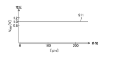
- a waveform 911 in FIG. 4 represents the time dependence of the reference voltage V REF according to the first reference example
- a waveform 912 in FIG. 5 represents the time dependence of the frequency f S1 of the signal S1 according to the first reference example.
- the reference voltage V REF according to the first reference example is fixed at 1.0 V (volt), and the frequency f S1 of the signal S1 is fixed at 2.0 MHz.
- the ramp voltage generation circuit 20 is set so that the frequency f S1 is fixed at 2.0 MHz. (increase slope U #RAMP , decrease slope D #RAMP , lower limit voltage V L#RAMP and upper limit voltage V H#RAMP described above) are defined.
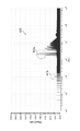
- FIG. 6 shows the frequency spectrum 913 of the signal S1 according to the first reference example.
- the signal S1 according to the first reference example has high-intensity signal components at the frequency of 2.0 MHz and its integer multiples. This means that high conducted and radiated noise occurs at those frequencies. High conducted and radiated noise is often unacceptable in various devices.
- the reference voltage VREF is a triangular voltage having a constant frequency.
- the frequency of this triangular wave is sufficiently lower than the frequency f S1 of signal S1. Therefore, in the second reference example, the frequency f S1 of the signal S1 fluctuates along with the fluctuation of the reference voltage VREF .
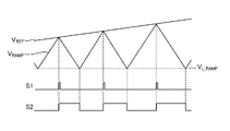
- FIG. 7 schematically shows waveforms of voltages and signals in the process in which the reference voltage V REF increases in one triangular wave when the first pattern (see FIG. 2) is adopted.
- the interval at which the rising edge of the signal S1 occurs gradually increases (that is, the frequency f S1 of the signal S1 gradually increases).
- FIG. 8 schematically shows waveforms of voltages and signals in the process in which the reference voltage V REF decreases in one triangular wave when the first pattern (see FIG. 2) is adopted.
- the interval at which the rising edge of the signal S1 occurs gradually decreases (that is, the frequency f S1 of the signal S1 gradually decreases).
- the peak intensity of signal S1 around the frequency of signal S1 decreases.
- a waveform 921 in FIG. 9 represents the time dependence of the reference voltage V REF according to the second reference example
- a waveform 922 in FIG. 10 represents the time dependence of the frequency f S1 of the signal S1 according to the second reference example.
- the reference voltage V REF according to the second reference example is a triangular voltage that varies from 0.8 V to 1.2 V centered at 1.0 V (volt), and the frequency of the triangular wave is 100 kHz. (kilohertz).
- the frequency f S1 of the signal S1 according to the second reference example fluctuates around 2.0 MHz.
- FIG. 11 shows the frequency spectrum 923 of the signal S1 according to the second reference example.
- the spectrum of the signal S1 is spread, and the peak intensity of the signal S1 in the high frequency band (the peak intensity at the frequencies of 2.0 MHz and integral multiples of 2.0 MHz) is reduced. (see dashed line portion 923a).
- the intensity of the signal S1 increases in the frequency band of modulation of the reference voltage VREF (corresponding to the dashed line portion 923b ).
- the frequency band of the modulation of the reference voltage V REF (here, the band around 100 kHz) is a low frequency band lower than the 2 MHz band, and noise in such a low frequency band affects the signal S1, the signal S1 or based on the signal S1.
- An example of a device that uses the signal S1 is a radar device mounted on a vehicle such as an automobile (hereinafter referred to as a vehicle-mounted radar device).
- An in-vehicle radar device can detect the distance between a vehicle and an object located outside the vehicle, the speed of the object (relative speed between the vehicle and the object), and the like.
- a large amount of noise in a low frequency band may adversely affect the detection accuracy of an onboard radar device.
- a method of using a voltage (see FIG. 12) that varies discretely using random numbers as the reference voltage VREF (this will be referred to as a third reference example) will also be considered.
- the circuit operation since the change in the reference voltage VREF is not stepwise, the circuit operation may be slow and the circuit may not function as intended. Alternatively, the circuit operation needs to be speeded up, which may increase the power consumption.
- the configuration of the switching device 1 capable of achieving characteristics superior to those of the above-described reference examples will be shown in the following multiple examples.
- the matters described above in the present embodiment are applied to each of the following examples unless otherwise stated and without contradiction.
- the description in each embodiment may take precedence.
- the matter described in any of the following embodiments can be applied to any other embodiment (i.e. any two or more of the embodiments). It is also possible to combine the examples of .
- Example EX1_A Example EX1_A will be described.
- the reference voltage V REF has a triangular waveform, and the reference voltage V REF is modulated such that the frequency of the triangular wave varies.
- FIG. 13 schematically shows a waveform 610 of the reference voltage VREF according to the embodiment EX1_A .
- the reference voltage generation circuit 10 according to this embodiment actually generates the reference voltage V REF in the embodiment EX1_A.
- the variation range of the reference voltage VREF is from a predetermined lower limit voltage VL#REF to a predetermined upper limit voltage VH#REF higher than the lower limit voltage VL#REF .
- the reference voltage generation circuit 10 according to Example EX1_A performs the following triangular wave generation unit operation.
- the reference voltage generation circuit 10 according to the embodiment EX1_A starts from a state in which the reference voltage V REF is matched with the predetermined lower limit voltage V L#REF , and changes the reference voltage V REF to the lower limit voltage V L#REF to the upper limit voltage VH#REF linearly and monotonically with an increasing slope U # REF .
- the reference voltage generating circuit 10 according to the embodiment EX1_A linearly and monotonously decreases the reference voltage VREF from the upper limit voltage VH#REF to the lower limit voltage VL#REF with a decreasing slope D#REF.
- One triangular wave generation unit operation starts from a state in which the reference voltage V REF is matched with the predetermined lower limit voltage V L#REF , and the reference voltage V REF monotonically increases and decreases until the reference voltage V REF reaches the lower limit voltage V This is the operation until returning to L#REF .
- the reference voltage generation circuit 10 according to the embodiment EX1_A repeatedly executes such a triangular wave generation unit operation. That is, in the i-th triangular wave generation unit operation, when the reference voltage V REF monotonically increases and decreases from the lower limit voltage V L#REF as a starting point and returns to the lower limit voltage V L_REF , the i-th triangular wave generation unit operation is performed. , the (i+1)th triangular wave generation unit operation is started.
- i represents any natural number.
- the period during which one triangular wave generation unit operation is performed is referred to as the triangular wave unit period
- the triangular wave unit period during which the i-th triangular wave generation unit operation is performed is denoted by the symbol "P[i]”. refer.
- the increasing slope U_REF and the decreasing slope D_REF have the same magnitude in each triangular wave generation unit operation. That is, in the i-th triangular wave generation unit operation (in other words, in the triangular wave unit period P[i]), the increasing slope U_REF and the decreasing slope D_REF are the same, and the (i+1)th triangular wave generation unit In operation (in other words in the triangular wave unit period P[i+1]) the increasing slope U_REF and the decreasing slope D_REF are the same as each other. The same applies to other triangular wave generation unit operations.
- the increasing slope U #REF and the decreasing slope D #REF in the (i+1)-th triangular wave generation unit operation are the increasing slope U #REF and the decreasing slope D #REF in the i-th triangular wave generation unit operation .
- #REF Different from #REF . That is, for any natural number i, the length of the triangular wave unit period P[i+1] differs from the length of the triangular wave unit period P[i], so the frequency of the triangular wave at the reference voltage VREF varies.
- n is an arbitrary integer of 2 or more.
- the length T[j+1] is longer than T[j] for any natural number j.
- the length of the triangular wave unit period is increased to length T[2] each time one triangular wave unit period elapses. ], T[3], . . . , T[n ⁇ 1], T[n].
- the length of the triangular wave unit period is changed from length T[1] to length T[2], T[3], . [n ⁇ 1] and T[n], and thereafter, the length of the triangular wave unit period is increased from T[n] to T[n] each time one triangular wave unit period elapses. [n ⁇ 1], T[n ⁇ 2], . . . , T[2], T[1], and this operation is repeated.
- the frequency of the triangular wave at the reference voltage VREF may be referred to as the frequency fREF .
- the frequency f REF can also be said to be the frequency of the reference voltage V REF . Focusing on the frequency fREF , the following can be said. That is, in the reference voltage generating circuit 10, the triangular wave frequency f REF is changed from the frequency "1/T[1]” to the frequency "1/T[2]", “1/T[ 3 ] ”, . Every time the period elapses, the frequency changes from the frequency "1/T[n]” to the frequency "1/T[n-1]", "1/T[n-2]", ..., "1/T[2] ”, and “1/T[1]”, and repeat this operation.
- frequency "1/T[1]” corresponds to the maximum frequency in the range of variation of frequency fREF
- frequency "1/T[ n]” corresponds to the minimum frequency in the variation range of the frequency fREF .
- the lengths T[1], T[2], T[3] are set to (1/120000) seconds, (1/100000) seconds, and (1/80000) seconds, respectively. seconds, where the triangular wave frequency f REF will vary between 120 kHz, 100 kHz and 80 kHz.
- the center frequency and the minimum frequency in the fluctuation range of the frequency f S1 of the signal S1 are It is sufficiently high (e.g. about ten times or several ten times) compared to the maximum frequency (ie "1/T[1]").
- the characteristics of the ramp voltage V RAMP increase slope U #RAMP , decrease slope D #RAMP , lower limit voltage V L#RAMP and upper limit voltage V H#RAMP ) should be appropriately set.
- the triangular wave frequency fREF is increased or decreased stepwise.
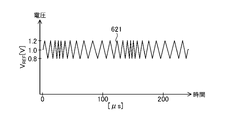
- a waveform 621 in FIG. 15 represents the time dependence of the reference voltage V REF according to the embodiment EX1_A
- a waveform 622 in FIG. 16 represents the time dependence of the frequency f S1 of the signal S1 according to the embodiment EX1_A.
- the reference voltage V REF according to Example EX1_A is a triangular voltage that varies from 0.8 V to 1.2 V centered at 1.0 V (volt)
- the frequency f REF of the triangular wave is Assume that the signal is modulated at around 100 kHz (kilohertz).
- "n 7"
- the lengths T[1], T[2], T[3], T[4], T[5], T[6], T[7] are 60, 80, 100, 120, respectively. , 140, 160, 180 kHz.
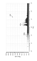
- FIG. 17 shows the frequency spectrum 623 of the signal S1 according to Example EX1_A.
- the spectrum of the signal S1 is spread in the embodiment EX1_A, and the peak intensity of the signal S1 in the high frequency band (2.0 MHz and integral multiples of 2.0 MHz) is reduced.
- the spectrum of the signal S1 is spread in the frequency band of the modulation of the reference voltage V REF (here, the band around 100 kHz), and the noise in this frequency band is also reduced. (see dashed line 923b in FIG. 11 and dashed line 623b in FIG. 17).
- the triangular wave of the reference voltage VREF is modulated.
- the peak intensity of the signal S1 in the high frequency band is also further reduced than in the second reference example (see dashed line portion 923a in FIG. 11 and dashed line portion 623a in FIG. 17).
- noise derived from the signal S1 (the The peak intensity of the noise and the switching noise of the switching transistor 50 based on the signal S1) can be reduced.
- Example EX1_B Example EX1_B will be described.
- FIG. 18 shows a configuration example of the reference voltage generation circuit 110 according to the embodiment EX1_B.
- Example EX1_B is implemented in combination with Example EX1_A described above, and the reference voltage generation circuit 110 is used as the reference voltage generation circuit 10 of Example EX1_A. That is, the reference voltage generation circuit 110 is an example of the reference voltage generation circuit 10 of Example EX1_A.
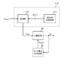
- the reference voltage generation circuit 110 includes a rectangular wave supply circuit 111 and a modulator 112 .
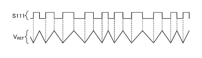
- the rectangular wave supply circuit 111 generates n types of rectangular wave signals having n types of frequencies different from each other, and outputs a signal S111 in which the n types of rectangular wave signals are combined.
- Signal S111 is input to modulator 112 .
- the signal S111 includes a first rectangular wave signal having a period of length T[1], a second rectangular wave signal having a period of length T[2], and a third rectangular wave signal having a period of length T[3]. It is a signal obtained by combining a rectangular wave signal and an n-th rectangular wave signal having a cycle of length T[n].
- Each of the first to n-th rectangular wave signals alternates between high and low signal levels. Assume here that the duty of each rectangular wave signal is 50%. That is, the ratio of the length of the high level period to the length of the low level period is 1:1 for each rectangular wave signal. It is also assumed that each period of each rectangular wave signal starts from a high level period.
- the type of rectangular wave signal incorporated in the signal S111 is switched for each period of each rectangular wave signal.
- one cycle of the first rectangular wave signal, one cycle of the second rectangular wave signal, one cycle of the third rectangular wave signal, A signal obtained by combining one period of the second rectangular wave signal in this order in the time-series direction is used as a unit signal, and the signal 111 is formed by repeating the unit signal.
- the frequency of the rectangular wave signal incorporated in the unit signal gradually decreases from the maximum frequency (reciprocal of length T[1]) to the minimum frequency (reciprocal of length T[n]) over time. , then gradually increases from the minimum frequency (reciprocal of the length T[n]) to the maximum frequency.
- a predetermined DC voltage V CNST is input to the modulator 112 .
- DC voltage V CNST has a fixed constant voltage.
- the modulator 112 modulates the DC voltage V CNST based on the signal S111 to generate the reference voltage V REF having the characteristics described in the embodiment EX1_A (see FIG. 13).
- the modulator 112 is arranged such that the reference voltage V REF linearly and monotonically increases with a predetermined increasing slope U # REF during the high level period of the signal S111, and the reference voltage V REF rises to a predetermined level during the low level period of the signal S111.
- the DC voltage V CNST is modulated based on the signal S111 so as to linearly and monotonously decrease at a decreasing slope D #REF of , thereby generating the reference voltage V REF .
- the modulator 112 makes the magnitudes of the increasing slope U #REF and the decreasing slope D #REF during the period when the i-th rectangular wave signal is input to the modulator 112 as the signal S111 proportional to the reciprocal of the length T[i]. Let That is, the modulator 112 sets the magnitude of the increasing slope U #REF and the decreasing slope D # REF during the period in which the first rectangular wave signal is input to the modulator 112 as the signal S111 to "(1/T[1])". ⁇ k B ”, and the magnitude of the increasing slope U #REF and the decreasing slope D #REF during the period when the second rectangular wave signal is input to the modulator 112 as the signal S111 is set to “(1/T[2] ) ⁇ k B ′′.
- the rectangular wave supply circuit 111 can also be configured with a rectangular wave generator 111a and a selector 111b.
- a signal S1 is input to the rectangular wave generator 111a.
- the rectangular wave generator 111a has a counter 111a_1 that counts the number of rising edges of the signal S1.
- the rectangular wave generator 111a generates first to n-th rectangular wave signals by dividing the frequency of the signal S1 by n kinds of frequency division ratios based on the count value of the counter 111a_1.
- the selector 111b outputs the signal S111 based on the first to n-th rectangular wave signals.
- the selector 111b selects one of the first to nth rectangular wave signals based on the selection signal SEL supplied from the rectangular wave generator 111a, and outputs the selected rectangular wave signal as the signal S111.
- the rectangular wave generator 111a generates the selection signal SEL based on the counter value so that the selector 111b outputs the signal S111 having the characteristics described above (for example, the signal S111 having the characteristics shown in FIG. 19). good.
- the selection signal SEL may be supplied to the selector 111b from a circuit other than the rectangular wave generator 111a.
- Example EX1_C will be described.
- FIG. 22 shows a configuration example of the reference voltage generation circuit 120 according to the embodiment EX1_C.
- Example EX1_C is implemented in combination with Example EX1_A described above, and reference voltage generation circuit 120 is used as reference voltage generation circuit 10 of Example EX1_A. That is, the reference voltage generation circuit 120 is an example of the reference voltage generation circuit 10 of Example EX1_A.
- the reference voltage generation circuit 120 includes a clock modulator 121 , a logic circuit 122 and a reference generator 123 .
- the clock modulator 121 has a VCO which is a voltage controlled oscillator, and the VCO generates a clock signal having a frequency according to the input voltage to itself.
- the clock signal is a square wave signal that alternates between high and low signal levels.
- the clock modulator 121 modulates the frequency of the clock signal by variably controlling the input voltage to the VCO (that is, fluctuates the frequency of the clock signal CLK, which will be described later).
- the modulated clock signal is supplied to the logic circuit 122 as the clock signal CLK.
- the logic circuit 122 supplies the reference generator 123 with a control signal S122 based on the clock signal CLK.
- the reference generator 123 generates a reference voltage VREF according to the control signal S122.
- the logic circuit 122 can divide the clock signal CLK by a predetermined division ratio and supply the divided clock signal CLK to the reference generator 123 as the control signal S122.
- the reference generator 123 generates the reference voltage V REF based on the control signal S122 such that the triangular wave frequency f REF in the reference voltage V REF is proportional to the frequency of the control signal S122.
- the frequency f REF of the triangular wave in the reference voltage V REF is set to k C times the frequency of the control signal S122.
- the frequency of the clock signal CLK is 20 MHz
- the frequency of the control signal S122 is 10 MHz
- the triangular wave frequency f REF is "(10 ⁇ k C )" MHz.
- the frequency of the clock signal CLK is 18 MHz
- the frequency of the control signal S122 is 9 MHz
- the triangular wave frequency f REF is "(9 ⁇ k C )" MHz.
- the triangular wave frequency f REF of the reference voltage V REF generated by the reference generator 123 depends on the frequency of the clock signal CLK.
- the clock signal CLK which is a frequency-modulated clock signal
- the frequency fREF of the triangular wave can be modulated.
- the modulated clock signal CLK may be generated so that the reference generator 123 generates the reference voltage VREF having the characteristics described in the embodiment EX1_A .
- the reference generator 123 may make the magnitudes of the increasing slope U #REF and the decreasing slope D #REF in the reference voltage V REF proportional to the frequency of the control signal S122, thereby making it proportional to the frequency of the clock signal CLK.
- a triangular wave frequency f REF is obtained.
- FIG. 23 is a configuration diagram of a switching power supply device 200 according to the second embodiment.
- the switching power supply device 200 is configured as a step-down DC/DC converter that power-converts an input voltage V IN to generate an output voltage V OUT that is lower than the input voltage V IN .
- Input voltage V IN and output voltage V OUT are positive DC voltages.
- the switching power supply device 200 is provided with an input terminal IN to which an input voltage V IN is applied, an output terminal OUT to which an output voltage V OUT is applied, a ground terminal GND having a ground potential, and a switch terminal SW to which a switch voltage V SW described later is applied. be done.
- the ground terminal GND and the switch terminal SW are provided on the lower potential side than the input terminal IN.
- the switching power supply device 200 includes the signal generation circuit 2 described in the first embodiment, as well as an output stage circuit 210 , a switching control circuit 220 , a rectification/smoothing circuit 230 and a feedback voltage generation circuit 240 .
- the signal generation circuit 2 in the switching power supply device 200 is the same as the signal generation circuit 2 (see FIG. 1) according to the first embodiment.
- the reference voltage VREF having the characteristics shown in the above-described embodiment EX1_A is generated, and the signal S1 is generated using this reference voltage VREF .
- the switching power supply device 200 can be configured using the semiconductor device 300 .
- FIG. 24 shows an example of the appearance of the semiconductor device 300.
- the semiconductor device 300 includes a semiconductor chip having a semiconductor integrated circuit formed on a semiconductor substrate, a housing (package) containing the semiconductor chip, and a plurality of external terminals exposed from the housing to the outside of the semiconductor device 300. and an electronic component.
- a semiconductor device 300 is formed by enclosing a semiconductor chip in a housing (package) made of resin.
- the semiconductor integrated circuit can include the signal generation circuit 2 , the output stage circuit 210 and the switching control circuit 220 , or can include the signal generation circuit 2 and the switching control circuit 220 .
- the feedback voltage generation circuit 240 may be provided inside the semiconductor device 300 or may be provided outside the semiconductor device 300 .
- the output stage circuit 210 has a half bridge circuit consisting of a series circuit of a high side transistor 211 and a low side transistor 212 .
- the rectifying/smoothing circuit 2 has an inductor 231 and an output capacitor 232 .
- the switching power supply 200 uses transistors 211 and 212 to perform DC-DC conversion in a synchronous rectification method.
- Transistors 211 and 212 are configured as N-channel MOSFETs. A modification is also possible in which the transistor 211 is configured as a P-channel MOSFET. Also, the transistor 212 can be replaced with a diode, in which case the switching power supply 200 performs DC-DC conversion by an asynchronous rectification method.
- the drain of transistor 211 is connected to input terminal IN and thus receives input voltage V IN .
- the source of the transistor 211 and the drain of the transistor 212 are commonly connected to the switch terminal SW.
- the source of transistor 212 is connected to ground terminal GND (ie, connected to ground).
- a voltage applied to the switch terminal SW is called a switch voltage and is represented by the symbol "V SW ".
- the switch terminal SW is connected to one end of the inductor 231, the other end of the inductor 231 is connected to the output terminal OUT, and the output voltage VOUT is generated at the output terminal OUT.
- An output capacitor 232 is connected between the output terminal OUT and ground.
- LD represents a load connected between the output terminal OUT and ground.
- Load LD is any load driven based on output voltage V OUT .
- the current flowing through the inductor 231 is called inductor current and is represented by the symbol "I L ".
- the feedback voltage generating circuit 240 generates a divided voltage of the output voltage V OUT using a series circuit of a plurality of resistors arranged between the output terminal OUT and the ground, and uses the generated divided voltage as the feedback voltage V FB in the switching control circuit. 220. However, it is also possible to use the output voltage VOUT itself as the feedback voltage VFB .
- the switching control circuit 220 controls and sets the state of the output stage circuit 210 to one of the output high state, output low state, and both off state.
- transistor 211 In the output high state, transistor 211 is on and transistor 212 is off.
- transistor 211 In the output low state, transistor 211 is off and transistor 212 is on.
- both off state both transistors 211 and 212 are off. Both transistors 211 and 212 are never turned on.
- the switching control circuit 220 alternately turns on and off the transistors 211 and 212 (that is, the output stage circuit 210 between an output high state and an output low state), thereby stabilizing the output voltage V OUT to a predetermined target voltage V TG . That is, the switching control circuit 220 can drive the transistors 211 and 212 in a so-called current mode control system. For example, the current flowing through the transistor 211 during the ON period of the transistor 211 can be used as information on the inductor current I L .
- turning on and off the transistors 211 and 212 alternately means that both off states are interposed between transitions between the output low state and the output high state in consideration of dead time. It is a concept that includes
- a rectangular wave voltage whose level substantially fluctuates between the level of the input voltage V IN and the level of the ground appears as the switch voltage V SW .
- the switch voltage VSW is rectified and smoothed by the rectifying/smoothing circuit 230 to obtain a DC output voltage VOUT .
- the switching control circuit 220 determines the switching frequencies of the transistors 211 and 212 based on the signal S1 output from the signal generating circuit 2.
- Switching control circuit 220 generates the other signals based on information about output voltage V OUT (ie, feedback voltage V FB ) and information about inductor current IL.
- the switching frequency of the transistors 211 and 212 is controlled based on the signal S1, and the output duty is controlled based on the other signals.
- the output duty represents the ratio of the period in which the output stage circuit 210 is in the output high state to the sum of the period in which the output stage circuit 210 is in the output high state and the period in which the output stage circuit 210 is in the output low state. Therefore, the switching control of the switching control circuit 220 corresponds to PWM control (pulse width modulation control).
- the switching control circuit 220 is an example of the switching control circuit 40 in FIG.
- the switching control circuit 220 includes the switching control circuit 40 of FIG. Noting that the transistor 211 is turned on by the switching control circuit 220 in synchronization with the rising edge of the signal S1, the transistor 211 corresponds to the switching transistor 50 in FIG. 211 switching operations are realized. Noting that the switching control circuit 220 turns off the transistor 212 in synchronization with the rising edge of the signal S1, the transistor 212 corresponds to the switching transistor 50 in FIG. A switching operation of 212 is realized.
- switching control circuit 220 employs a method of controlling the state of output stage circuit 210 based on information on output voltage V OUT (that is, feedback voltage V FB ) without referring to information on inductor current IL. Also good.
- the switching power supply device 200 configured as a step-down DC/DC converter is taken as an example, the switching power supply device 200 can also be configured as a step-up DC/DC converter or a buck-boost DC/DC converter. .
- the power supply that generates the power supply voltage for the in-vehicle radar system is strongly required to have low noise.
- large noise in a low frequency band (for example, a band around 100 kHz) may adversely affect various capabilities (for example, detection accuracy) of the vehicle-mounted radar device.
- the switching power supply device 200 shown in the second embodiment is suitable as a power supply device for an in-vehicle radar device. That is, the load LD in FIG. 23 may be an in-vehicle radar device.
- the load LD is not limited to an in-vehicle radar device.
- the load LD may be various sensor devices that are not classified as radar devices, or may be arbitrary electronic devices.
- the switching power supply device 200 is useful as a power supply device for any load LD that requires low noise (particularly, for example, low noise in a low frequency band).
- any of the transistors described above may be any type of transistor as long as there is no inconvenience.
- any transistor described above as a MOSFET can be replaced with a junction FET, an IGBT (Insulated Gate Bipolar Transistor), or a bipolar transistor as long as it does not cause any inconvenience.
- Any transistor has a first electrode, a second electrode and a control electrode.
- a FET one of the first and second electrodes is the drain and the other is the source, and the control electrode is the gate.
- an IGBT one of the first and second electrodes is the collector and the other is the emitter, and the control electrode is the gate.
- a bipolar transistor not belonging to an IGBT one of the first and second electrodes is the collector and the other is the emitter and the control electrode is the base.
- first physical quantity and an arbitrary second physical quantity are “the same” is interpreted as a concept that includes an error. That is, that the first physical quantity and the second physical quantity are “the same” means that the design or manufacturing is aimed at making the first physical quantity and the second physical quantity “the same”. and the second physical quantity, it should be understood that the first physical quantity and the second physical quantity are "the same”. This applies not only to physical quantities.
- a signal generation circuit includes a reference voltage generation circuit configured to generate a reference voltage, a ramp voltage generation circuit configured to generate a ramp voltage that fluctuates within a predetermined voltage range, and the reference and a comparison circuit configured to output a comparison result signal representing the magnitude relationship between the voltage and the lamp voltage, wherein the reference voltage generation circuit causes the reference voltage to have a triangular waveform, and the triangular wave. is a configuration (first configuration) for varying the frequency of .
- the comparison circuit In the signal generation circuit according to the first configuration, the comparison circuit generates a specific change in the comparison result signal when the ramp voltage transitions from a state lower than the reference voltage to a state higher than the reference voltage. and the ramp voltage generation circuit monotonically increases the ramp voltage from a predetermined lower limit voltage with a predetermined increasing slope, and increases the ramp voltage toward the lower limit voltage when the specific change occurs in the comparison result signal.
- a configuration (second configuration) in which a unit operation of monotonously decreasing at a predetermined decreasing slope is repeatedly executed may be used.
- the comparison circuit In the signal generation circuit according to the first configuration, the comparison circuit generates a specific change in the comparison result signal when the ramp voltage transitions from a state higher than the reference voltage to a state lower than the reference voltage. and the ramp voltage generating circuit monotonously decreases the ramp voltage from a predetermined upper limit voltage with a predetermined decreasing slope, and when the comparison result signal undergoes the specific change, the ramp voltage is directed toward the upper limit voltage.
- a configuration (third configuration) in which a unit operation that monotonically increases with a predetermined increasing gradient is repeatedly executed may be used.
- the reference voltage generation circuit sequentially uses a plurality of rectangular wave signals having frequencies different from each other to modulate a predetermined DC voltage.
- a configuration (fourth configuration) for generating a reference voltage may be employed.
- the reference voltage generation circuit causes the triangular wave in the reference voltage to have a frequency corresponding to the frequency of a clock signal, and sets the frequency of the clock signal to A configuration (fifth configuration) in which the frequency of the triangular wave is changed by modulation may be employed.
- a switching device includes a signal generation circuit according to any one of the first to fifth configurations, a switching transistor, and a switching control configured to switch the switching transistor based on the comparison result signal. and a circuit (sixth configuration).
- a switching device includes a signal generation circuit according to the second or third configuration, a switching transistor, a switching control circuit configured to switch the switching transistor based on the comparison result signal, wherein the switching control circuit turns on or off the switching transistor triggered by the specific change in the comparison result signal (seventh configuration).
- the switching control circuit changes the state of the switching transistor from one of an ON state and an OFF state to the other state in response to the specific change in the comparison result signal. and then, when a predetermined condition is established, the switching operation of returning the state of the switching transistor from the other state to the one state is repeated (eighth configuration).
- a switching power supply device is a switching power supply device configured to generate an output voltage from an input voltage, comprising the switching device according to the eighth configuration, wherein a terminal to which the input voltage is applied and the terminal The switching transistor is arranged between a terminal provided on a lower potential side than the switching transistor, and the output voltage is generated by power-converting the input voltage through the switching operation (a ninth configuration).
- switching device 2 signal generation circuit 10 reference voltage generation circuit 20 lamp voltage generation circuit 30 comparison circuit 40 switching control circuit 50 switching transistor 110 reference voltage generation circuit 111 rectangular wave supply circuit 112 modulator 111a rectangular wave generation section 111a_1 counter 111b selector 120 Reference voltage generation circuit 121 Clock modulator 122 Logic circuit 123 Reference generator V REF reference voltage V RAMP ramp voltage S1 Signal (comparison result signal)
Landscapes
- Engineering & Computer Science (AREA)
- Power Engineering (AREA)
- Physics & Mathematics (AREA)
- Electromagnetism (AREA)
- Dc-Dc Converters (AREA)
Abstract
Description
本開示の第1実施形態を説明する。図1は本開示の第1実施形態に係るスイッチング装置1の構成図である。スイッチング装置1は、基準電圧生成回路10と、ランプ電圧生成回路20と、比較回路30と、スイッチング制御回路40と、スイッチングトランジスタ50と、を備える。スイッチング装置1は、スペクトラム拡散信号生成回路と称することもできる信号生成回路2を内包している。信号生成回路2は、基準電圧生成回路10、ランプ電圧生成回路20及び比較回路30を備えて構成される。
図2に、第1パターンにおける基準電圧VREF及びランプ電圧VRAMP並びに信号S1の関係を示す。図2には信号S2も示されているが、信号S2については後述される。上述したように、基準電圧VREFは三角波の波形を有しているが、基準電圧VREFの周波数(換言すれば基準電圧VREFにおける三角波の周波数)はランプ電圧VRAMPの周波数よりも随分と小さいため、図2では、基準電圧VREFの値が一定であるかのように各電圧波形が図示されている(後述の図3でも同様)。
図3に、第2パターンにおける基準電圧VREF及びランプ電圧VRAMP並びに信号S1の関係を示す。図3には信号S2も示されているが、信号S2については後述される。
スイッチング制御回路40の動作は上述の第1パターン及び第2パターン間で共通である。スイッチング制御回路40は信号S1のアップエッジを契機に(換言すれば信号S1のアップエッジに同期して)スイッチングトランジスタ50をターンオン又はターンオフさせる。
第1参考例では基準電圧VREFを一定電圧で固定する。このため、第1参考例では信号S1の周波数fS1も一定に固定される。図4の波形911は第1参考例に係る基準電圧VREFの時間依存性を表し、図5の波形912は第1参考例に係る信号S1の周波数fS1の時間依存性を表す。ここでは、第1参考例に係る基準電圧VREFは1.0V(ボルト)に固定され、信号S1の周波数fS1は2.0MHzで固定される。尚、第1参考例に限らず、本実施形態では、基準電圧VREFが1.0Vで固定されると仮定したとき、周波数fS1が2.0MHzで固定されるよう、ランプ電圧生成回路20の特性(上記の増加傾きU#RAMP、減少傾きD#RAMP、下限電圧VL#RAMP及び上限電圧VH#RAMP)が定められていることを想定する。
第2参考例では基準電圧VREFを一定の周波数を有する三角波状の電圧とする。この三角波の周波数は信号S1の周波数fS1よりも十分に低い。このため、第2参考例では信号S1の周波数fS1が基準電圧VREFの変動に連れて変動する。
乱数を用いて離散的に変動する電圧(図12参照)を基準電圧VREFとして用いる方法(これを第3参考例と称する)も検討される。しかしながら、第3参考例では、基準電圧VREFの変化が段階的でないため、回路動作がおいつかず、思惑通りに機能しないこともある。或いは、回路動作の高速化を必要とし、消費電力が増大するおそれがある。
実施例EX1_Aを説明する。実施例EX1_Aにおいて、基準電圧VREFは三角波の波形を有し、更に、その三角波の周波数が変動するように基準電圧VREFが変調される。図13に実施例EX1_Aに係る基準電圧VREFの波形610を模式的に示す。本実施形態に係る基準電圧生成回路10は、実際には、実施例EX1_Aにおける基準電圧VREFを生成する。
実施例EX1_Bを説明する。図18に実施例EX1_Bに係る基準電圧生成回路110の構成例を示す。実施例EX1_Bは上述の実施例EX1_Aと組み合わせて実施され、基準電圧生成回路110は実施例EX1_Aの基準電圧生成回路10として利用される。即ち、基準電圧生成回路110は実施例EX1_Aの基準電圧生成回路10の一例である。
実施例EX1_Cを説明する。図22に実施例EX1_Cに係る基準電圧生成回路120の構成例を示す。実施例EX1_Cは上述の実施例EX1_Aと組み合わせて実施され、基準電圧生成回路120は実施例EX1_Aの基準電圧生成回路10として利用される。即ち、基準電圧生成回路120は実施例EX1_Aの基準電圧生成回路10の一例である。
本開示の第2実施形態を説明する。第2実施形態は第1実施形態と組み合わせて実施される。図23は第2実施形態に係るスイッチング電源装置200の構成図である。スイッチング電源装置200は、入力電圧VINを電力変換することにより入力電圧VINよりも低い出力電圧VOUTを生成する降圧型DC/DCコンバータとして構成されている。入力電圧VIN及び出力電圧VOUTは正の直流電圧である。スイッチング電源装置200には、入力電圧VINが加わる入力端子IN、出力電圧VOUTが加わる出力端子OUT、グランド電位を有するグランド端子GND、及び、後述のスイッチ電圧VSWが加わるスイッチ端子SWが設けられる。グランド端子GND及びスイッチ端子SWは入力端子INよりも低電位側に設けられる。
本開示の第3実施形態を説明する。第3実施形態では上述の第1又は第2実施形態に適用可能な応用技術又は変形技術等を説明する。
本開示について付記を設ける。
2 信号生成回路
10 基準電圧生成回路
20 ランプ電圧生成回路
30 比較回路
40 スイッチング制御回路
50 スイッチングトランジスタ
110 基準電圧生成回路
111 矩形波供給回路
112 変調器
111a 矩形波生成部
111a_1 カウンタ
111b セレクタ
120 基準電圧生成回路
121 クロック変調器
122 ロジック回路
123 基準発生器
VREF 基準電圧
VRAMP ランプ電圧
S1 信号(比較結果信号)
Claims (9)
- 基準電圧を生成するように構成された基準電圧生成回路と、
所定電圧範囲内で変動するランプ電圧を生成するように構成されたランプ電圧生成回路と、
前記基準電圧及び前記ランプ電圧の高低関係を表す比較結果信号を出力するように構成された比較回路と、を備え、
前記基準電圧生成回路は、前記基準電圧に三角波の波形を持たせ、且つ、前記三角波の周波数を変動させる
、信号生成回路。 - 前記比較回路は、前記ランプ電圧が前記基準電圧よりも低い状態から前記基準電圧よりも高い状態へ遷移したとき、前記比較結果信号に特定変化を発生させ、
前記ランプ電圧生成回路は、前記ランプ電圧を所定の下限電圧から所定の増加傾きにて単調増加させ、前記比較結果信号に前記特定変化が生じると、前記ランプ電圧を前記下限電圧に向けて所定の減少傾きにて単調減少させる単位動作を繰り返し実行する
、請求項1に記載の信号生成回路。 - 前記比較回路は、前記ランプ電圧が前記基準電圧よりも高い状態から前記基準電圧よりも低い状態へ遷移したとき、前記比較結果信号に特定変化を発生させ、
前記ランプ電圧生成回路は、前記ランプ電圧を所定の上限電圧から所定の減少傾きにて単調減少させ、前記比較結果信号に前記特定変化が生じると、前記ランプ電圧を前記上限電圧に向けて所定の増加傾きにて単調増加させる単位動作を繰り返し実行する
、請求項1に記載の信号生成回路。 - 前記基準電圧生成回路は、互いに異なる周波数を有する複数の矩形波信号を順次用いて、所定の直流電圧を変調することにより前記基準電圧を生成する
、請求項1~3の何れかに記載の信号生成回路。 - 前記基準電圧生成回路は、前記基準電圧における前記三角波にクロック信号の周波数に応じた周波数を持たせ、前記クロック信号の周波数を変調することで前記三角波の周波数を変動させる
、請求項1~3の何れかに記載の信号生成回路。 - 請求項1~5の何れかに記載の信号生成回路と、
スイッチングトランジスタと、
前記比較結果信号に基づいて前記スイッチングトランジスタをスイッチングさせるように構成されたスイッチング制御回路と、を備える
、スイッチング装置。 - 請求項2又は3に記載の信号生成回路と、
スイッチングトランジスタと、
前記比較結果信号に基づいて前記スイッチングトランジスタをスイッチングさせるように構成されたスイッチング制御回路と、を備え、
前記スイッチング制御回路は、前記比較結果信号における前記特定変化を契機に前記スイッチングトランジスタをターンオン又はターンオフさせる
、スイッチング装置。 - 前記スイッチング制御回路は、前記比較結果信号における前記特定変化を契機に前記スイッチングトランジスタの状態をオン状態及びオフ状態の内の一方の状態から他方の状態へと変化させ、その後、所定条件の成立を契機に前記スイッチングトランジスタの状態を前記他方の状態から前記一方の状態に戻すスイッチング動作を繰り返す
、請求項7に記載のスイッチング装置。 - 入力電圧から出力電圧を生成するように構成されたスイッチング電源装置であって、
請求項8に記載のスイッチング装置を備え、
前記入力電圧が加わる端子と前記端子よりも低電位側に設けられた端子との間に前記スイッチングトランジスタを配置し、前記スイッチング動作を通じて前記入力電圧を電力変換することにより前記出力電圧を生成する
、スイッチング電源装置。
Priority Applications (4)
| Application Number | Priority Date | Filing Date | Title |
|---|---|---|---|
| JP2023535161A JPWO2023286459A1 (ja) | 2021-07-16 | 2022-05-25 | |
| DE112022002598.0T DE112022002598T5 (de) | 2021-07-16 | 2022-05-25 | Signalerzeugungsschaltung, schalteinrichtung und schaltnetzteil |
| CN202280049122.2A CN117642974A (zh) | 2021-07-16 | 2022-05-25 | 信号生成电路、开关装置和开关电源装置 |
| US18/392,460 US20240162817A1 (en) | 2021-07-16 | 2023-12-21 | Signal generation circuit, switching device, and switching power supply device |
Applications Claiming Priority (2)
| Application Number | Priority Date | Filing Date | Title |
|---|---|---|---|
| JP2021117614 | 2021-07-16 | ||
| JP2021-117614 | 2021-07-16 |
Related Child Applications (1)
| Application Number | Title | Priority Date | Filing Date |
|---|---|---|---|
| US18/392,460 Continuation US20240162817A1 (en) | 2021-07-16 | 2023-12-21 | Signal generation circuit, switching device, and switching power supply device |
Publications (1)
| Publication Number | Publication Date |
|---|---|
| WO2023286459A1 true WO2023286459A1 (ja) | 2023-01-19 |
Family
ID=84919923
Family Applications (1)
| Application Number | Title | Priority Date | Filing Date |
|---|---|---|---|
| PCT/JP2022/021398 Ceased WO2023286459A1 (ja) | 2021-07-16 | 2022-05-25 | 信号生成回路、スイッチング装置及びスイッチング電源装置 |
Country Status (5)
| Country | Link |
|---|---|
| US (1) | US20240162817A1 (ja) |
| JP (1) | JPWO2023286459A1 (ja) |
| CN (1) | CN117642974A (ja) |
| DE (1) | DE112022002598T5 (ja) |
| WO (1) | WO2023286459A1 (ja) |
Citations (6)
| Publication number | Priority date | Publication date | Assignee | Title |
|---|---|---|---|---|
| JP2001013233A (ja) * | 1999-06-29 | 2001-01-19 | Kenwood Corp | ジッタ信号発生器 |
| JP2003324944A (ja) * | 2002-05-08 | 2003-11-14 | Fuji Electric Co Ltd | 電源回路 |
| JP2004266780A (ja) * | 2003-03-04 | 2004-09-24 | Fuji Electric Device Technology Co Ltd | パルス幅変調回路 |
| JP2013255309A (ja) * | 2012-06-05 | 2013-12-19 | Rohm Co Ltd | モータ駆動回路およびそれを用いた電子機器 |
| JP2014230210A (ja) * | 2013-05-24 | 2014-12-08 | 船井電機株式会社 | Pwm変調回路 |
| JP2018164401A (ja) * | 2018-07-25 | 2018-10-18 | 新電元工業株式会社 | 制御装置 |
Family Cites Families (6)
| Publication number | Priority date | Publication date | Assignee | Title |
|---|---|---|---|---|
| US7928715B2 (en) * | 2008-04-22 | 2011-04-19 | Seiko Instruments Inc. | Switching regulator |
| KR20150137323A (ko) * | 2014-05-29 | 2015-12-09 | 인제대학교 산학협력단 | 이중 모드 dc-dc 벅 컨버터 |
| JP6815127B2 (ja) | 2015-09-08 | 2021-01-20 | ローム株式会社 | Dc/dcコンバータ、スイッチング電源装置 |
| US10135369B2 (en) * | 2015-09-29 | 2018-11-20 | Microchip Technology Incorporated | Linear hall effect sensors for multi-phase permanent magnet motors with PWM drive |
| US10333403B2 (en) * | 2016-06-28 | 2019-06-25 | Dialog Semiconductor (Uk) Limited | Adaptive on-time switching converter |
| US10826397B2 (en) * | 2018-09-03 | 2020-11-03 | Rohm Co., Ltd. | Switching power supply operable in an intermittent driving mode |
-
2022
- 2022-05-25 WO PCT/JP2022/021398 patent/WO2023286459A1/ja not_active Ceased
- 2022-05-25 DE DE112022002598.0T patent/DE112022002598T5/de active Pending
- 2022-05-25 CN CN202280049122.2A patent/CN117642974A/zh active Pending
- 2022-05-25 JP JP2023535161A patent/JPWO2023286459A1/ja active Pending
-
2023
- 2023-12-21 US US18/392,460 patent/US20240162817A1/en active Pending
Patent Citations (6)
| Publication number | Priority date | Publication date | Assignee | Title |
|---|---|---|---|---|
| JP2001013233A (ja) * | 1999-06-29 | 2001-01-19 | Kenwood Corp | ジッタ信号発生器 |
| JP2003324944A (ja) * | 2002-05-08 | 2003-11-14 | Fuji Electric Co Ltd | 電源回路 |
| JP2004266780A (ja) * | 2003-03-04 | 2004-09-24 | Fuji Electric Device Technology Co Ltd | パルス幅変調回路 |
| JP2013255309A (ja) * | 2012-06-05 | 2013-12-19 | Rohm Co Ltd | モータ駆動回路およびそれを用いた電子機器 |
| JP2014230210A (ja) * | 2013-05-24 | 2014-12-08 | 船井電機株式会社 | Pwm変調回路 |
| JP2018164401A (ja) * | 2018-07-25 | 2018-10-18 | 新電元工業株式会社 | 制御装置 |
Also Published As
| Publication number | Publication date |
|---|---|
| DE112022002598T5 (de) | 2024-03-07 |
| US20240162817A1 (en) | 2024-05-16 |
| CN117642974A (zh) | 2024-03-01 |
| JPWO2023286459A1 (ja) | 2023-01-19 |
Similar Documents
| Publication | Publication Date | Title |
|---|---|---|
| US6353309B1 (en) | Switching circuit having a switching semiconductor device and control method thereof | |
| US10910026B2 (en) | Clock generation circuit, switching power supply device, and semiconductor device | |
| US10892684B2 (en) | Circuit for a switching power supply | |
| US12483134B2 (en) | Buck converter circuit with seamless PWM/PFM transition | |
| CN106877846B (zh) | 一种脉冲产生电路、开关电源电路及平均电流计算方法 | |
| JP2018129907A (ja) | Dc/dcコンバータおよびその制御回路、制御方法、車載電装機器 | |
| CN110896275B (zh) | 升降压电源转换器及用于控制升降压电源转换器的方法和驱动器 | |
| CN116937978B (zh) | 一种cot控制电路 | |
| US20250088104A1 (en) | Driver for slew-rate control of phase node in buck converter | |
| CN116995913A (zh) | 多相dc/dc转换器控制装置及多相dc/dc转换器 | |
| US11637489B2 (en) | Isolated DC/DC converter and AC/DC converter | |
| JP2023174083A (ja) | スイッチング電源用回路及びスイッチング電源装置 | |
| WO2023286459A1 (ja) | 信号生成回路、スイッチング装置及びスイッチング電源装置 | |
| CN100463345C (zh) | 开关稳压器的控制电路、使用其的电源装置以及电子设备 | |
| KR100426606B1 (ko) | Dc ―dc 컨버터 및 이를 사용한 전자장치 | |
| US20210328504A1 (en) | Driving circuit with emi reduction | |
| US20230213959A1 (en) | Clock signal generation circuit, dc/dc converter, pwm signal generator, and vehicle | |
| JP7812852B2 (ja) | アンプ回路、スイッチング電源用回路及びスイッチング電源装置 | |
| JP2025176834A (ja) | 電源制御装置及び電源装置 | |
| US20250383683A1 (en) | Clock Signal Generation Circuit, Semiconductor Device, Semiconductor System, and Power Supply Control Device | |
| US20260058558A1 (en) | Clock signal generation circuit, power supply control device, and switching power supply device | |
| US20250038669A1 (en) | Semiconductor Device, Semiconductor System and Switching Power Device | |
| JP2025153495A (ja) | 信号生成回路、スイッチング制御回路、スイッチング電源装置、及び車両 | |
| JP2024083792A (ja) | 電源制御装置 | |
| JP2025187604A (ja) | 電源制御装置及びスイッチング電源装置 |
Legal Events
| Date | Code | Title | Description |
|---|---|---|---|
| 121 | Ep: the epo has been informed by wipo that ep was designated in this application |
Ref document number: 22841806 Country of ref document: EP Kind code of ref document: A1 |
|
| WWE | Wipo information: entry into national phase |
Ref document number: 2023535161 Country of ref document: JP |
|
| WWE | Wipo information: entry into national phase |
Ref document number: 202280049122.2 Country of ref document: CN |
|
| WWE | Wipo information: entry into national phase |
Ref document number: 112022002598 Country of ref document: DE |
|
| 122 | Ep: pct application non-entry in european phase |
Ref document number: 22841806 Country of ref document: EP Kind code of ref document: A1 |