WO2023282317A1 - 電子部品収納用パッケージ及び電子装置 - Google Patents
電子部品収納用パッケージ及び電子装置 Download PDFInfo
- Publication number
- WO2023282317A1 WO2023282317A1 PCT/JP2022/026926 JP2022026926W WO2023282317A1 WO 2023282317 A1 WO2023282317 A1 WO 2023282317A1 JP 2022026926 W JP2022026926 W JP 2022026926W WO 2023282317 A1 WO2023282317 A1 WO 2023282317A1
- Authority
- WO
- WIPO (PCT)
- Prior art keywords
- lid
- electronic component
- component storage
- base
- storage package
- Prior art date
- Legal status (The legal status is an assumption and is not a legal conclusion. Google has not performed a legal analysis and makes no representation as to the accuracy of the status listed.)
- Ceased
Links
Images





Classifications
-
- G—PHYSICS
- G02—OPTICS
- G02B—OPTICAL ELEMENTS, SYSTEMS OR APPARATUS
- G02B6/00—Light guides; Structural details of arrangements comprising light guides and other optical elements, e.g. couplings
- G02B6/24—Coupling light guides
- G02B6/42—Coupling light guides with opto-electronic elements
-
- H—ELECTRICITY
- H01—ELECTRIC ELEMENTS
- H01S—DEVICES USING THE PROCESS OF LIGHT AMPLIFICATION BY STIMULATED EMISSION OF RADIATION [LASER] TO AMPLIFY OR GENERATE LIGHT; DEVICES USING STIMULATED EMISSION OF ELECTROMAGNETIC RADIATION IN WAVE RANGES OTHER THAN OPTICAL
- H01S5/00—Semiconductor lasers
- H01S5/02—Structural details or components not essential to laser action
- H01S5/022—Mountings; Housings
- H01S5/0225—Out-coupling of light
- H01S5/02251—Out-coupling of light using optical fibres
-
- H—ELECTRICITY
- H01—ELECTRIC ELEMENTS
- H01S—DEVICES USING THE PROCESS OF LIGHT AMPLIFICATION BY STIMULATED EMISSION OF RADIATION [LASER] TO AMPLIFY OR GENERATE LIGHT; DEVICES USING STIMULATED EMISSION OF ELECTROMAGNETIC RADIATION IN WAVE RANGES OTHER THAN OPTICAL
- H01S5/00—Semiconductor lasers
- H01S5/02—Structural details or components not essential to laser action
- H01S5/022—Mountings; Housings
- H01S5/0225—Out-coupling of light
- H01S5/02253—Out-coupling of light using lenses
-
- H—ELECTRICITY
- H10—SEMICONDUCTOR DEVICES; ELECTRIC SOLID-STATE DEVICES NOT OTHERWISE PROVIDED FOR
- H10W—GENERIC PACKAGES, INTERCONNECTIONS, CONNECTORS OR OTHER CONSTRUCTIONAL DETAILS OF DEVICES COVERED BY CLASS H10
- H10W76/00—Containers; Fillings or auxiliary members therefor; Seals
- H10W76/10—Containers or parts thereof
-
- H—ELECTRICITY
- H10—SEMICONDUCTOR DEVICES; ELECTRIC SOLID-STATE DEVICES NOT OTHERWISE PROVIDED FOR
- H10W—GENERIC PACKAGES, INTERCONNECTIONS, CONNECTORS OR OTHER CONSTRUCTIONAL DETAILS OF DEVICES COVERED BY CLASS H10
- H10W99/00—Subject matter not provided for in other groups of this subclass
Definitions
- the present disclosure relates to an electronic component storage package and an electronic device.
- Japanese Patent Application Laid-Open No. 2001-044316 discloses a device having a ceramic substrate having a semiconductor chip mounting portion and a sealing resin covering the mounting portion.
- the electronic component storage package includes: a substrate having an electronic component mounting portion on its upper surface; a lid covering the mounting portion; with The substrate is made of ceramic, The lid is made of resin and has locking pieces that can be locked to the base.
- An electronic device includes: the electronic component storage package; an electronic component housed in the electronic component housing package; Prepare.
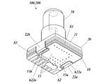
- FIG. 1 is an exploded perspective view showing an electronic component storage package and an electronic device according to Embodiment 1 of the present disclosure
- FIG. 2 is a perspective view of the electronic component storage package and the electronic device of Embodiment 1 as viewed from below
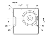
- FIG. 1 is a plan view showing an electronic component housing package and an electronic device according to Embodiment 1.
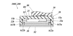
- FIG. 4 is a cross-sectional view taken along line AA of FIG. 3;
- FIG. 4 is a cross-sectional view showing a state in which the base and the lid are separated;
- FIG. 10 is a perspective view showing a lid with a connector according to Embodiment 2 of the present disclosure;
- FIG. 10 is a cross-sectional view showing an electronic component storage package and an electronic device according to Embodiment 3 of the present disclosure
- FIG. 10 is a cross-sectional view showing an electronic component storage package of Modification 1 according to the present disclosure
- FIG. 10 is a cross-sectional view showing a lid of an electronic component storage package according to Modification 2 of the present disclosure
- FIG. 11 is a cross-sectional view of an electronic component storage package of Modification 2 with a lid attached.
- FIG. 11 is a side view showing an electronic component storage package of Modification 3 according to the present disclosure
- FIG. 11 is a side view showing an electronic component storage package of Modification 4 according to the present disclosure
- FIG. 11 is a plan view showing an electronic component storage package of Modification 5 according to the present disclosure;
- FIG. 1 is an exploded perspective view showing an electronic device and an electronic component storage package according to Embodiment 1 of the present disclosure.
- FIG. 2 is a perspective view of the electronic component storage package and the electronic device of Embodiment 1 as viewed from below.
- FIG. 3 is a plan view showing the electronic component storage package and the electronic device according to the first embodiment. 4 and 5 are cross-sectional views taken along the line AA of FIG. 3.
- FIG. 5 shows the state in which the base and the lid are separated.
- An electronic component storage package 100 of Embodiment 1 includes a base 10 having a mounting portion 11 for an electronic component 80 , a lid 20 covering the mounting portion 11 of the base 10 , and an optical connector 30 fixed to the lid 20 .
- the electronic component 80 may be an optical element that emits light, such as a VCSEL (Vertical Cavity Surface Emitting Laser), a semiconductor laser, or a light-emitting diode, or an optical element that receives light, such as a photodiode. may be an optical element.
- the electronic component 80 may be an electronic component other than an optical element.
- circuit components, optical components, and the like may be mounted on the mounting portion 11 of the base 10.
- the electronic component 80 may be configured to emit light upward or receive light from above, either alone or in cooperation with an optical component such as a mirror or prism.
- the light may be laser light.
- the direction facing the first surface S1 from the second surface S2 (FIG. 2) of the substrate 10 will be described as upward. The direction of each part shown in the embodiment does not have to match the direction when the electronic device 200 is used.
- the substrate 10 has a first surface (upper surface) S1, a second surface (lower surface) S2 located on the opposite side of the first surface S1, and a side surface S3 located between the first surface S1 and the second surface S2.
- the base 10 may have a concave portion H1 that opens upward, and the mounting portion 11 may be positioned in the concave portion H1.
- the base 10 is made of a ceramic material such as an aluminum oxide sintered body, a mullite sintered body, a silicon carbide sintered body, an aluminum nitride sintered body, or a silicon nitride sintered body.
- a glass-ceramic material may be employed as the ceramic material.
- the substrate 10 may be configured by laminating ceramic materials.
- the substrate 10 has an electrode 12 (FIG. 1) located on the first surface S1, an electrode 13 (FIG. 2) located on the second surface S2, and an internal conductor (not shown) located inside.
- a signal, a power supply voltage, or both of these may be exchanged between the outside of the base 10 and the components mounted on the mounting portion 11 via the electrodes 12 and 13 and the internal conductors. Since the substrate 10 is made of a ceramic material, a high-frequency signal can be applied as the signal.
- the base 10 may further have grooves 15a, 15b in which the locking pieces 22a, 22b of the lid 20 are locked.
- the grooves 15a and 15b may be located on the side surface S3 of the base 10, or may be located from the side surface S3 to the second surface (lower surface) S2.
- the side surface S3 on which one groove 15a is located and the side surface S3 on which the other groove 15b is located may be sides facing in opposite directions, or may face in opposite directions.
- the lid 20 has a base portion 21 that covers the mounting portion 11 and locking pieces 22 a and 22 b that are locked to the base 10 .
- the lid 20 is made of resin.
- the resin may be transparent. Being transparent allows light to pass between the inside and outside of the mounting portion 11 through the lid 20 without providing an opening in the lid 20 .
- the base 21 may be plate-shaped.
- the base 21 and the locking pieces 22a and 22b may be integrally molded.
- locking pieces 22 a and 22 b can be fitted into the grooves 15 a and 15 b of the base 10 to lock the lid 20 to the base 10 .
- “locking” may mean a state in which the lid 20 does not come off the base 10 even when the base 10 is turned upside down due to the frictional force between the locking pieces 22a, 22b and the base 10.
- the locking pieces 22a and 22b may be plate-shaped and extend from the base 21 in the direction along the side surface S3 of the base 10.
- the lid 20 has two locking pieces 22a and 22b, but may have one or three or more locking pieces.
- the plurality of locking pieces 22a and 22b may be arranged so as to face the plurality of side faces S3 of the base 10 facing in different directions, or face the plurality of side faces S3 facing the opposite sides of the base 10. may be arranged to
- the locking pieces 22 a and 22 b may be arranged at positions corresponding to the grooves 15 a and 15 b of the base 10 .
- the locking pieces 22a and 22b are composed of body portions (first portions) j22a and j22b positioned facing the side surface S3 of the base 10 and claws h22a and h22b extending inward of the base 10. (Second part).
- the grooves 15a and 15b of the base 10 may have stepped portions h15a and h15b on which the claws h22a and h22b are hooked.
- the stepped portions h15a and h15b When a force in the direction of separating the lid 20 from the base 10 is applied by the claws h22a and h22b and the stepped portions h15a and h15b, the stepped portions h15a and h15b generate a reaction force in the opposite direction to the pulling force from the stepped portions h15a and h15b to the claws h22a and h22b. works.
- one groove 15a of the base 10 has an inner surface S4a positioned along the second surface S2, and the claw h22a may contact the inner surface S4a.
- the other groove 15b may have an inner surface S4b located along the second surface S2, and the other claw h22b may contact the inner surface S4b.
- the expression that the surface A is along the surface B means that if both the surface A and the surface B are plane surfaces, the surface A and the surface B are closer to parallel than orthogonal. If B is not a plane, it means that the angle formed by the average normal direction of surface A and the average normal direction of surface B is closer to 0° than 90°.
- the claws h22a and h22b are in contact with the inner surfaces S4a and S4b of the grooves 15a and 15b, so that when a force is applied to separate the lid 20 from the base 10, a reaction force in the opposite direction to the force is applied to the grooves 15a and 15b. from the inner surfaces S4a, S4b of the claws h22a, h22b.
- the dimension Ln2 of the claw h22a in the extending direction of the claw h22a may be smaller than the dimension Ln1 of the body j22a in the extending direction of the claw h22a.
- the same may be applied to the other locking piece 22b.
- the relationship between the dimensions Ln1 and Ln2 facilitates attachment of the lid 20 to the base 10 and reduces the possibility of the locking pieces 22a and 22b being damaged when the lid 20 is removed from the base 10.
- the claw h22a of one locking piece 22a may have a tapered portion t22a.
- the tapered portion t22a may have a shape in which the dimension of the tapered portion t22a in the direction in which the claw h22a extends decreases as the distance from the first surface S1 of the base 10 increases.
- the claw h22b of the other locking piece 22b may also have a similar tapered portion t22b.
- the tapered portions t22a and t22b can improve the assembling properties of the locking pieces 22a and 22b into the grooves 15a and 15b.
- bonding strength can be improved by filling the space (gap c3, FIG. 4) created between the tapered portions t22a and t22b and the base 10 with the bonding material.
- the optical connector 30 is a connector to which an optical fiber can be connected.
- the optical connector 30 may be a receptacle having a hole 31 into which the tip of the optical fiber is fitted.
- the hole 31 may have a cylindrical shape, and the extension of the hole 31 serves as an optical path through which light passes.
- the optical connector 30 may be made of resin, and the resin may be transparent. By being transparent, it is possible to integrally configure the portion through which light passes and the portion for connecting the connection counterpart, thereby reducing the manufacturing cost of the optical connector 30 .
- Optical connector 30 may be of the same material as lid 20 .
- the optical connector 30 is not limited to the illustrated optical receptacle, and may be an optical receptacle of another standard, or an optical plug of a predetermined standard.
- the optical connector 30 may be an optical pigtail.
- An optical pigtail is a configuration that includes a fiber optic cable and an optical connector attached to one end of the fiber optic cable.
- the cable end of the optical pigtail may be fixed to the lid 20 via an optical receptacle, or the cable end of the optical pigtail may be fixed to the lid 20 by means other than the optical receptacle. good.
- the optical connector 30 When the optical connector 30 is made of resin, the optical connector 30 may be integrally formed with the lid 20 by injection molding or the like. Alternatively, the optical connector 30 may be molded separately from the lid 20 and joined to the lid 20 after molding. A resin bonding material may be used for the bonding. With the configuration in which the optical connector 30 is joined to the lid 20 , the fixed position of the optical connector 30 can be adjusted with high accuracy according to the optical axis of the components of the mounting portion 11 after the lid 20 and the optical connector 30 are molded.
- the optical connector 30 may include a lens 32 on the optical path, as shown in FIG.
- the lens 32 may be integrally molded with the optical connector 30 .
- the lens 32 may have a configuration in which the end surface of the hole 31 in the optical connector 30 and the surface facing the lid 20 have a lens surface shape to exert a lens action.
- the lid 20 may have a lens instead of the lens 32 of the optical connector 30.
- the lens may be formed integrally with the lid 20, or may be composed of a transparent resin portion sandwiched between the surface of the lid 20 on the optical connector 30 side and the surface on the base 10 side. That is, the surface of the lid 20 on the optical connector 30 side and the surface on the base 10 side of the lid 20 may have a lens surface shape to exert a lens effect.
- the lens may be positioned on the extension of the optical path of the optical connector 30 .
- An electronic device 200 includes an electronic component storage package 100 and an electronic component 80 stored in the electronic component storage package 100 .
- the electronic component 80 may be mounted on the mounting portion 11 of the base 10 .
- the electronic device 200 is assembled as follows. First, an electronic component storage package 100 in which the base 10 and the lid 20 are separated is prepared. At this stage, the optical connector 30 may already be fixed to the lid 20 . Components including the electronic component 80 are mounted on the mounting portion 11 of the base 10 . After the components including the electronic components 80 are mounted, the lid 20 is attached to the base 10 . During the attachment, the locking pieces 22a and 22b of the lid 20 are fitted into the grooves 15a and 15b of the base 10, and the claws h22a and h22b of the locking pieces 22a and 22b are caught by the stepped portions h15a and h15b. A lid 20 is locked to the base 10 . Further, the lid 20 is stably locked to the base 10 by the claws h22a and h22b of the locking pieces 22a and 22b contacting the inner surfaces S4a and S4b in the grooves 15a and 15b.
- a bonding material is applied to the opposing portion c1 between the first surface S1 of the base 10 and the lid 20, and to the inside c2 of the grooves 15a and 15b.
- the bonding material may be made of resin.
- a gap c3 may be provided between the stepped portions h15a, h15b of the grooves 15a, 15b and the claws h22a, h22b of the locking pieces 22a, 22b.
- the joint between the claws h22a and h22b and the stepped portions h15a and h15b may be strengthened by accumulating the joint material in the gap c3.
- the assembly of the electronic device 200 is completed by curing the bonding material.
- the electronic device 200 may be mounted on a module substrate, for example.
- the electrodes on the second surface S2 of the base 10 may be bonded to the electrodes of the module substrate via a bonding material such as solder.
- a lead pin may be connected to the second surface S2 of the substrate 10, passed through a through hole of the module substrate, and bonded via a bonding material such as solder.
- an optical fiber may be connected to the optical connector 30 of the electronic device 200 .
- the lid 20 is made of resin
- the manufacturing cost of the lid 20 can be reduced, and the cost of the electronic component storage package 100 can be reduced.
- the lid 20 is made of resin
- the base 10 is made of ceramic
- the lid 20 has the locking pieces 22a and 22b and the locking pieces 22a and 22b are locked to the base 10, the lid 20 and the base 10 can be joined with high strength. Therefore, the electronic component storage package 100 in which the lid 20 and the base 10 are joined can realize a robust configuration.
- the optical connector 30 fixed to the lid 20
- a component such as an optical fiber that introduces or leads out light
- the optical connector 30 is made of resin
- the difference in the amount of thermal expansion between the optical connector 30 and the lid 20 caused by temperature changes can be reduced, and warping or cracking of the lid 20 and the optical connector 30 can be prevented. can be suppressed.
- the lid 20 is transparent, the light can be emitted from the mounting portion 11 to the outside of the package through the lid 20 without providing an opening through which light passes through the lid 20 . Or vice versa, light can pass through. Therefore, the manufacturing cost of the lid 20 can be reduced by reducing the number of molding steps of the lid 20 .
- the electronic component storage package 100 of the first embodiment by having the lens 32 integrally configured with the optical connector 30 and a single member, compared with the case where the lens 32 is provided separately, the electronic component storage package 100 can The component cost of the component storage package 100 can be reduced. In addition, compared to the case where the lens 32 is separately provided, the stress generated around the lens 32 due to temperature change can be suppressed, and a robust structure of the electronic component storage package 100 including the optical connector 30 is realized. can.
- the electronic component storage package 100 of Embodiment 1 may have a lens that is integrally configured with the lid 20 and a single member. , the component cost of the electronic component storage package 100 can be reduced. Furthermore, compared to the case where a lens is provided separately, the stress generated around the lens due to temperature change can be reduced, and a robust configuration of the electronic component storage package 100 can be realized.
- the electronic device 200 of the first embodiment by having the electronic component storage package 100, it is possible to reduce the cost of the electronic device 200 and realize a robust configuration of the electronic device 200. Furthermore, the lid 20 and the periphery of the mounting portion 11 of the base body 10 and the locking pieces 22a and 22b and the base body 10 are bonded via a bonding material, so that the lid 20 and the base body 10 are bonded together. The bonding strength is improved, and the electronic device 200 can have a more robust configuration. With this configuration, even if a separating force is applied between the base 10 and the lid 20, it is possible to prevent the lid 20 from being detached or easily displaced.
- FIG. 6 is a perspective view showing a lid with a connector according to Embodiment 2 of the present disclosure.
- the lid 20A is made of a resin material containing radio wave absorbing material. Components other than the material of the lid 20A are the same as those of the first embodiment.
- Carbon, ferrite, nickel, etc. can be applied as radio wave absorbing materials.
- a general molding method for resin materials such as injection molding can be applied to the resin material into which the radio wave absorbing material is kneaded. Therefore, the lid 20A of the second embodiment can be manufactured in the same manner as in the first embodiment.
- the lid 20A containing radio wave absorbing material has low transparency or is non-transparent. Therefore, the lid 20 ⁇ /b>A may have a transparent portion 25 ( FIG. 6 ) through which light passes in a portion facing the mounting portion 11 .
- the transparent portion 25 may be a through-hole or transparent resin.
- the transparent portion 25 can be formed by molding in the case of a through hole, and can be formed by molding using two kinds of resin materials in the case of a transparent resin.
- the lid 20A containing the radio wave absorbing material prevents electromagnetic noise from propagating from the component mounted on the mounting portion 11 to the outside of the package or vice versa (EMI). : Electromagnetic Interference) can be reduced. Further, since the lid 20 ⁇ /b>A has the transparent portion 25 , light can pass through the transparent portion 25 from the mounting portion 11 to the outside of the package or vice versa.
- FIG. 7 is a cross-sectional view showing an electronic component storage package and an electronic device according to Embodiment 3 of the present disclosure.
- the lid 20B and the optical connector 30B are made of a resin material containing radio wave absorbing material.
- the radio wave absorbing material is the same as that shown in the second embodiment.
- the same components as those in Embodiment 1 are denoted by the same reference numerals, and detailed description thereof is omitted.
- the optical connector 30B containing radio wave absorbing material has low transparency or is non-transparent. Therefore, the optical connector 30B has a transparent portion 33 in the portion of the optical path on the extension line of the hole 31. As shown in FIG.
- the transparent portion 33 may be made of transparent resin.
- the lid 20B containing the radio wave absorbing material has low transparency or is non-transparent. Accordingly, the lid 20B has an aperture 26 that allows light to pass through.
- a lens 41 may be fixed in the opening 26 .
- the lens 41 may be made of resin, or may be made of a material other than resin, such as glass.
- the transparent portion 33 of the optical connector 30B may function as a lens by being molded into a lens shape.
- the optical connector 30B containing the radio wave absorbing material by having the optical connector 30B containing the radio wave absorbing material, electromagnetic noise is transmitted from the component mounted on the mounting portion 11 to the outside of the package, or vice versa. It is possible to suppress failures such as propagation. Furthermore, light can pass from the mounting portion 11 to the outside of the package or vice versa through the transparent portion 33 of the optical connector 30B and the opening 26 and the lens 41 of the lid 20B.
- FIG. 8A is a cross-sectional view showing an electronic component storage package of Modification 1 according to the present disclosure.
- the cross-sectional view shows a cross-section along line AA in FIG.
- the grooves 15a and 15b of the base 10 may be positioned on the side surface S3 and may be separated from the second surface S2. Further, the grooves 15a, 15b may be spaced apart from the second surface S2 of the substrate 10.
- the locking pieces 22a and 22b may have the same configuration as in the first embodiment. According to this configuration, when the locking pieces 22a and 22b are fitted into the grooves 15a and 15b and attached, the bonding material applied between the locking pieces 22a and 22b and the base 10 is applied to the second surface S2 of the base 10. can reduce leakage.
- FIG. 8B is a cross-sectional view showing the lid of the electronic component storage package of Modification 2 according to the present disclosure
- FIG. 8C is a cross-sectional view of the electronic component storage package of Modification 2 to which the lid is attached.
- the locking pieces 22 a and 22 b of the lid 20 may not have claws protruding inward from the base 10 .
- the locking pieces 22a and 22b having no hooks have a horizontal spacing L1 (FIG. 8B) at the tips when the locking pieces 22a and 22b are not fitted to the base 10, and are equal to the inner wall surfaces of the grooves 15a and 15b of the base 10. It may be smaller than width L2 (FIG. 8C).
- L1 horizontal spacing
- FIG. 8C width L2
- FIG. 9A is a side view showing an electronic component storage package of Modification 3 according to the present disclosure.
- FIG. 9B is a side view showing an electronic component storage package of Modification 4 according to the present disclosure.
- the claw h22c of the locking piece 22a may protrude in the direction along the side surface S3 of the base 10.
- the claw h22c may have a shape that protrudes in the horizontal direction in a stepped manner.
- the claw h22c has a tapered portion t22c
- the tapered portion t22c has a shape in which the horizontal dimension of the tapered portion t22c increases as the distance from the first surface S1 of the base 10 increases.
- the groove 15a of the base 10 has a shape corresponding to the locking piece 22a and the claw h22c. The same applies to the locking piece 22b and the groove 15b on the opposite side.
- the lid 20 and the base 10 can be locked with high strength by hooking the claws h22c on the grooves 15a and 15b.
- FIG. 10 is a plan view showing an electronic component storage package of Modification 5 according to the present disclosure.
- the arrangement of the locking pieces 22a and 22b of the lid 20 may be changed.
- the side surface S3 of the base 10 has a plurality of sections a to d
- the locking pieces 22a and 22b may be positioned in the two sections b and d facing each other as in the first to third embodiments.
- one locking piece 22a may be positioned farther from the optical connector 30 in the section d.
- the two locking pieces 22a and 22b may be positioned diagonally on one side and the other on either side of the center of the base 10 when viewed from above.
- the grooves 15a and 15b of the base 10 may be arranged at positions corresponding to the locking pieces 22a and 22b.
- the locking piece 22a may be located in the section c far from the optical connector 30. Furthermore, the locking piece 22a may be positioned in the center of the section c. With this arrangement, the lid 20 and the base 10 can be stably locked by the locking piece 22a. Furthermore, the stress applied to the lid 20 via the locking piece 22a is reduced from acting on the connecting portion between the lid 20 and the optical connector 30, and deterioration of the connecting portion can be reduced.
- the arrangement of the locking pieces 22a and 22b is not limited to the above example.
- the arrangement of the locking pieces 22a and 22b may be determined according to the joint position between the base 10 (FIG. 1) and the module board, or the connection position of the lead pin if the lead pin is connected to the base 10.
- the locking pieces 22a and 22b may be arranged on the opposite side across the center of the base 10 in plan view with respect to the joining position with the module substrate or the connecting position of the lead pin.
- the electronic component may be a component other than an optical element, and the electronic component storage package may not have an optical connector fixed to the lid.
- the base may have no groove, and the engaging piece of the lid may be engaged with the side surface of the base.
- the details shown in the embodiments, such as the shape of the lid and the shape of the base, can be changed as appropriate without departing from the scope of the present disclosure.
- the present disclosure can be used for electronic component storage packages and electronic devices.
Landscapes
- Physics & Mathematics (AREA)
- General Physics & Mathematics (AREA)
- Optics & Photonics (AREA)
- Condensed Matter Physics & Semiconductors (AREA)
- Electromagnetism (AREA)
- Optical Couplings Of Light Guides (AREA)
Priority Applications (1)
| Application Number | Priority Date | Filing Date | Title |
|---|---|---|---|
| JP2023533182A JPWO2023282317A1 (https=) | 2021-07-07 | 2022-07-07 |
Applications Claiming Priority (2)
| Application Number | Priority Date | Filing Date | Title |
|---|---|---|---|
| JP2021-112557 | 2021-07-07 | ||
| JP2021112557 | 2021-07-07 |
Publications (1)
| Publication Number | Publication Date |
|---|---|
| WO2023282317A1 true WO2023282317A1 (ja) | 2023-01-12 |
Family
ID=84800773
Family Applications (1)
| Application Number | Title | Priority Date | Filing Date |
|---|---|---|---|
| PCT/JP2022/026926 Ceased WO2023282317A1 (ja) | 2021-07-07 | 2022-07-07 | 電子部品収納用パッケージ及び電子装置 |
Country Status (2)
| Country | Link |
|---|---|
| JP (1) | JPWO2023282317A1 (https=) |
| WO (1) | WO2023282317A1 (https=) |
Citations (8)
| Publication number | Priority date | Publication date | Assignee | Title |
|---|---|---|---|---|
| JP2000121885A (ja) * | 1998-10-20 | 2000-04-28 | Fujikura Ltd | 光モジュールの電磁波対策構造 |
| JP2001296451A (ja) * | 2000-04-14 | 2001-10-26 | Hosiden Corp | 光コネクタレセプタクルおよびこれを具備した携帯型電子機器 |
| JP2005005614A (ja) * | 2003-06-13 | 2005-01-06 | Matsushita Electric Ind Co Ltd | 半導体装置およびその製造方法 |
| JP2006030813A (ja) * | 2004-07-21 | 2006-02-02 | Citizen Electronics Co Ltd | 光ファイバモジュール |
| JP2009229613A (ja) * | 2008-03-20 | 2009-10-08 | Murata Mfg Co Ltd | 光モジュール |
| WO2013047354A1 (ja) * | 2011-09-26 | 2013-04-04 | 日本電気株式会社 | 中空封止構造 |
| US20130313415A1 (en) * | 2012-05-22 | 2013-11-28 | Hon Hai Precision Industry Co., Ltd. | Easily assembled optical-electrical converting device |
| JP2015162473A (ja) * | 2014-02-26 | 2015-09-07 | 京セラ株式会社 | 受発光素子モジュール |
-
2022
- 2022-07-07 WO PCT/JP2022/026926 patent/WO2023282317A1/ja not_active Ceased
- 2022-07-07 JP JP2023533182A patent/JPWO2023282317A1/ja active Pending
Patent Citations (8)
| Publication number | Priority date | Publication date | Assignee | Title |
|---|---|---|---|---|
| JP2000121885A (ja) * | 1998-10-20 | 2000-04-28 | Fujikura Ltd | 光モジュールの電磁波対策構造 |
| JP2001296451A (ja) * | 2000-04-14 | 2001-10-26 | Hosiden Corp | 光コネクタレセプタクルおよびこれを具備した携帯型電子機器 |
| JP2005005614A (ja) * | 2003-06-13 | 2005-01-06 | Matsushita Electric Ind Co Ltd | 半導体装置およびその製造方法 |
| JP2006030813A (ja) * | 2004-07-21 | 2006-02-02 | Citizen Electronics Co Ltd | 光ファイバモジュール |
| JP2009229613A (ja) * | 2008-03-20 | 2009-10-08 | Murata Mfg Co Ltd | 光モジュール |
| WO2013047354A1 (ja) * | 2011-09-26 | 2013-04-04 | 日本電気株式会社 | 中空封止構造 |
| US20130313415A1 (en) * | 2012-05-22 | 2013-11-28 | Hon Hai Precision Industry Co., Ltd. | Easily assembled optical-electrical converting device |
| JP2015162473A (ja) * | 2014-02-26 | 2015-09-07 | 京セラ株式会社 | 受発光素子モジュール |
Also Published As
| Publication number | Publication date |
|---|---|
| JPWO2023282317A1 (https=) | 2023-01-12 |
Similar Documents
| Publication | Publication Date | Title |
|---|---|---|
| US12181723B2 (en) | Optical waveguide package and light-emitting device | |
| US8867869B2 (en) | Miniaturized high speed optical module | |
| CN100383574C (zh) | 带有集成透镜的封装和包括该封装的组件 | |
| CN102200614B (zh) | 光学轴线在封装件内垂直地弯折的光学组件 | |
| US7384202B2 (en) | Optical module | |
| JP2005294808A (ja) | 光送信アセンブリの製造方法 | |
| WO2021014568A1 (ja) | To-can型光送信モジュール | |
| CN110391586A (zh) | 发射器组件 | |
| CN113281857B (zh) | 光半导体器件及光模块 | |
| CN105093437B (zh) | 光传送模块 | |
| US9063309B2 (en) | Optoelectronic module with flexible substrate | |
| US10928599B2 (en) | Optical sub-assembly for a module communicating over optical fiber, with a device for optical coupling aligned in a passive manner | |
| CN107658691B (zh) | 光半导体装置 | |
| WO2023282317A1 (ja) | 電子部品収納用パッケージ及び電子装置 | |
| US8581173B2 (en) | Fiber optic transceiver module having a molded cover in which an optical beam transformer made of an elastomer is integrally formed | |
| CN113341513B (zh) | 光模块 | |
| US20220007496A1 (en) | Optical module | |
| CN116148987A (zh) | 硅光子光学收发装置 | |
| US12222540B2 (en) | Optical waveguide package and light-emitting device | |
| JP2006054457A (ja) | オプトエレクトロニクス部品用ハウジング及び光学アセンブリ | |
| CN116560013A (zh) | 多通道光器件及光模块 | |
| US20150338275A1 (en) | Optical Transmission Module | |
| US20250167188A1 (en) | Optical waveguide board, optical waveguide package, and light source module | |
| JP2018018995A (ja) | 光モジュール | |
| JP2016020937A (ja) | 光電気変換装置、およびそれを用いた信号伝送装置 |
Legal Events
| Date | Code | Title | Description |
|---|---|---|---|
| 121 | Ep: the epo has been informed by wipo that ep was designated in this application |
Ref document number: 22837731 Country of ref document: EP Kind code of ref document: A1 |
|
| WWE | Wipo information: entry into national phase |
Ref document number: 2023533182 Country of ref document: JP |
|
| NENP | Non-entry into the national phase |
Ref country code: DE |
|
| 122 | Ep: pct application non-entry in european phase |
Ref document number: 22837731 Country of ref document: EP Kind code of ref document: A1 |