WO2023282168A1 - 露光装置 - Google Patents
露光装置 Download PDFInfo
- Publication number
- WO2023282168A1 WO2023282168A1 PCT/JP2022/026201 JP2022026201W WO2023282168A1 WO 2023282168 A1 WO2023282168 A1 WO 2023282168A1 JP 2022026201 W JP2022026201 W JP 2022026201W WO 2023282168 A1 WO2023282168 A1 WO 2023282168A1
- Authority
- WO
- WIPO (PCT)
- Prior art keywords
- scanning direction
- predetermined range
- exposure
- substrate
- exposing
- Prior art date
- Legal status (The legal status is an assumption and is not a legal conclusion. Google has not performed a legal analysis and makes no representation as to the accuracy of the status listed.)
- Ceased
Links
Images




Classifications
-
- G—PHYSICS
- G03—PHOTOGRAPHY; CINEMATOGRAPHY; ANALOGOUS TECHNIQUES USING WAVES OTHER THAN OPTICAL WAVES; ELECTROGRAPHY; HOLOGRAPHY
- G03F—PHOTOMECHANICAL PRODUCTION OF TEXTURED OR PATTERNED SURFACES, e.g. FOR PRINTING, FOR PROCESSING OF SEMICONDUCTOR DEVICES; MATERIALS THEREFOR; ORIGINALS THEREFOR; APPARATUS SPECIALLY ADAPTED THEREFOR
- G03F7/00—Photomechanical, e.g. photolithographic, production of textured or patterned surfaces, e.g. printing surfaces; Materials therefor, e.g. comprising photoresists; Apparatus specially adapted therefor
- G03F7/70—Microphotolithographic exposure; Apparatus therefor
- G03F7/70216—Mask projection systems
- G03F7/70358—Scanning exposure, i.e. relative movement of patterned beam and workpiece during imaging
-
- G—PHYSICS
- G02—OPTICS
- G02B—OPTICAL ELEMENTS, SYSTEMS OR APPARATUS
- G02B26/00—Optical devices or arrangements for the control of light using movable or deformable optical elements
- G02B26/08—Optical devices or arrangements for the control of light using movable or deformable optical elements for controlling the direction of light
- G02B26/0816—Optical devices or arrangements for the control of light using movable or deformable optical elements for controlling the direction of light by means of one or more reflecting elements
- G02B26/0833—Optical devices or arrangements for the control of light using movable or deformable optical elements for controlling the direction of light by means of one or more reflecting elements the reflecting element being a micromechanical device, e.g. a MEMS mirror, DMD
-
- G—PHYSICS
- G03—PHOTOGRAPHY; CINEMATOGRAPHY; ANALOGOUS TECHNIQUES USING WAVES OTHER THAN OPTICAL WAVES; ELECTROGRAPHY; HOLOGRAPHY
- G03F—PHOTOMECHANICAL PRODUCTION OF TEXTURED OR PATTERNED SURFACES, e.g. FOR PRINTING, FOR PROCESSING OF SEMICONDUCTOR DEVICES; MATERIALS THEREFOR; ORIGINALS THEREFOR; APPARATUS SPECIALLY ADAPTED THEREFOR
- G03F7/00—Photomechanical, e.g. photolithographic, production of textured or patterned surfaces, e.g. printing surfaces; Materials therefor, e.g. comprising photoresists; Apparatus specially adapted therefor
- G03F7/20—Exposure; Apparatus therefor
-
- G—PHYSICS
- G03—PHOTOGRAPHY; CINEMATOGRAPHY; ANALOGOUS TECHNIQUES USING WAVES OTHER THAN OPTICAL WAVES; ELECTROGRAPHY; HOLOGRAPHY
- G03F—PHOTOMECHANICAL PRODUCTION OF TEXTURED OR PATTERNED SURFACES, e.g. FOR PRINTING, FOR PROCESSING OF SEMICONDUCTOR DEVICES; MATERIALS THEREFOR; ORIGINALS THEREFOR; APPARATUS SPECIALLY ADAPTED THEREFOR
- G03F7/00—Photomechanical, e.g. photolithographic, production of textured or patterned surfaces, e.g. printing surfaces; Materials therefor, e.g. comprising photoresists; Apparatus specially adapted therefor
- G03F7/70—Microphotolithographic exposure; Apparatus therefor
- G03F7/70216—Mask projection systems
- G03F7/70258—Projection system adjustments, e.g. adjustments during exposure or alignment during assembly of projection system
-
- G—PHYSICS
- G03—PHOTOGRAPHY; CINEMATOGRAPHY; ANALOGOUS TECHNIQUES USING WAVES OTHER THAN OPTICAL WAVES; ELECTROGRAPHY; HOLOGRAPHY
- G03F—PHOTOMECHANICAL PRODUCTION OF TEXTURED OR PATTERNED SURFACES, e.g. FOR PRINTING, FOR PROCESSING OF SEMICONDUCTOR DEVICES; MATERIALS THEREFOR; ORIGINALS THEREFOR; APPARATUS SPECIALLY ADAPTED THEREFOR
- G03F7/00—Photomechanical, e.g. photolithographic, production of textured or patterned surfaces, e.g. printing surfaces; Materials therefor, e.g. comprising photoresists; Apparatus specially adapted therefor
- G03F7/70—Microphotolithographic exposure; Apparatus therefor
- G03F7/70216—Mask projection systems
- G03F7/70283—Mask effects on the imaging process
- G03F7/70291—Addressable masks, e.g. spatial light modulators [SLMs], digital micro-mirror devices [DMDs] or liquid crystal display [LCD] patterning devices
-
- G—PHYSICS
- G03—PHOTOGRAPHY; CINEMATOGRAPHY; ANALOGOUS TECHNIQUES USING WAVES OTHER THAN OPTICAL WAVES; ELECTROGRAPHY; HOLOGRAPHY
- G03F—PHOTOMECHANICAL PRODUCTION OF TEXTURED OR PATTERNED SURFACES, e.g. FOR PRINTING, FOR PROCESSING OF SEMICONDUCTOR DEVICES; MATERIALS THEREFOR; ORIGINALS THEREFOR; APPARATUS SPECIALLY ADAPTED THEREFOR
- G03F7/00—Photomechanical, e.g. photolithographic, production of textured or patterned surfaces, e.g. printing surfaces; Materials therefor, e.g. comprising photoresists; Apparatus specially adapted therefor
- G03F7/70—Microphotolithographic exposure; Apparatus therefor
- G03F7/70483—Information management; Active and passive control; Testing; Wafer monitoring, e.g. pattern monitoring
- G03F7/70491—Information management, e.g. software; Active and passive control, e.g. details of controlling exposure processes or exposure tool monitoring processes
- G03F7/70508—Data handling in all parts of the microlithographic apparatus, e.g. handling pattern data for addressable masks or data transfer to or from different components within the exposure apparatus
-
- G—PHYSICS
- G03—PHOTOGRAPHY; CINEMATOGRAPHY; ANALOGOUS TECHNIQUES USING WAVES OTHER THAN OPTICAL WAVES; ELECTROGRAPHY; HOLOGRAPHY
- G03F—PHOTOMECHANICAL PRODUCTION OF TEXTURED OR PATTERNED SURFACES, e.g. FOR PRINTING, FOR PROCESSING OF SEMICONDUCTOR DEVICES; MATERIALS THEREFOR; ORIGINALS THEREFOR; APPARATUS SPECIALLY ADAPTED THEREFOR
- G03F7/00—Photomechanical, e.g. photolithographic, production of textured or patterned surfaces, e.g. printing surfaces; Materials therefor, e.g. comprising photoresists; Apparatus specially adapted therefor
- G03F7/70—Microphotolithographic exposure; Apparatus therefor
- G03F7/70691—Handling of masks or workpieces
- G03F7/70716—Stages
- G03F7/70725—Stages control
-
- G—PHYSICS
- G03—PHOTOGRAPHY; CINEMATOGRAPHY; ANALOGOUS TECHNIQUES USING WAVES OTHER THAN OPTICAL WAVES; ELECTROGRAPHY; HOLOGRAPHY
- G03F—PHOTOMECHANICAL PRODUCTION OF TEXTURED OR PATTERNED SURFACES, e.g. FOR PRINTING, FOR PROCESSING OF SEMICONDUCTOR DEVICES; MATERIALS THEREFOR; ORIGINALS THEREFOR; APPARATUS SPECIALLY ADAPTED THEREFOR
- G03F7/00—Photomechanical, e.g. photolithographic, production of textured or patterned surfaces, e.g. printing surfaces; Materials therefor, e.g. comprising photoresists; Apparatus specially adapted therefor
- G03F7/70—Microphotolithographic exposure; Apparatus therefor
- G03F7/70691—Handling of masks or workpieces
- G03F7/70758—Drive means, e.g. actuators, motors for long- or short-stroke modules or fine or coarse driving
Definitions
- a step-and-repeat projection exposure apparatus such as liquid crystal and organic EL display panels and semiconductor elements (integrated circuits, etc.
- And-scan projection exposure apparatuses so-called scanning steppers (also called scanners)
- This type of exposure apparatus projects and exposes a mask pattern for an electronic device onto a photosensitive layer coated on the surface of a substrate to be exposed (hereinafter simply referred to as a substrate) such as a glass substrate, semiconductor wafer, printed wiring board, or resin film. are doing.
- a digital mirror device or the like in which a large number of micromirrors that are slightly displaced are regularly arranged can be used instead of the mask substrate.
- a digital mirror device or the like in which a large number of micromirrors that are slightly displaced are regularly arranged.
- illumination light obtained by mixing light from a laser diode (LD) with a wavelength of 375 nm and light from an LD with a wavelength of 405 nm in a multimode fiber bundle is sent to a digital mirror.
- a device (DMD) is irradiated with light, and reflected light from each of a large number of tilt-controlled micromirrors is projected and exposed onto a substrate via an imaging optical system and a microlens array.
- the exposure apparatus it is desired to achieve high-precision exposure with high throughput.
- an exposure apparatus includes a substrate holder that holds and moves a substrate, a spatial light modulator that has light modulation elements arranged two-dimensionally, and an illumination that irradiates illumination light onto the spatial light modulator.
- a projection unit that guides the illumination light from the light modulation element to each of light irradiation area groups that are two-dimensionally arranged on the substrate in a first direction and in a second direction perpendicular to the first direction; and a controller for driving the substrate holder in the scanning direction, wherein the light modulation element is oriented at a predetermined angle ⁇ (0° ⁇ ⁇ 90°), and the controller controls the center of the illumination light emitted from each of the light modulation elements irradiated within the predetermined range when exposing the predetermined range of the substrate.
- the substrate holder is scanned at such a speed that the spot positions indicating are staggered.
- FIG. 1 is a perspective view showing an overview of the external configuration of an exposure apparatus according to one embodiment.
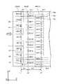
- FIG. 2 is a diagram showing an arrangement example of a DMD projection area projected onto a substrate by each projection unit of a plurality of exposure modules.
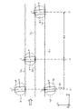
- FIG. 3 is a diagram for explaining the state of stitch exposure by each of the four specific projection areas in FIG.
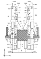
- FIG. 4 is an optical layout diagram of a specific configuration of two exposure modules arranged in the X direction (scanning exposure direction) viewed in the XZ plane.
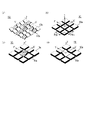
- FIG. 5(a) is a diagram schematically showing the DMD
- FIG. 5(b) is a diagram showing the DMD when the power is off
- FIG. 5(c) is an explanation of the mirrors in the ON state.
- FIG. 5(a) is a diagram schematically showing the DMD
- FIG. 5(b) is a diagram showing the DMD when the power is off
- FIG. 5(c) is an explanation of the mirrors in the ON state.
- FIG. 5D is a diagram for explaining the mirror in the OFF state.
- FIG. 6 is a diagram showing a schematic configuration of an alignment device provided on a calibration reference portion attached to the edge of the substrate holder of the exposure apparatus.
- FIG. 7 is a diagram schematically showing a projection area (light irradiation area group) and an exposure target area (area where a line pattern is exposed) on the substrate.
- FIG. 8 is a diagram showing a rectangular area that is part of a linear exposure target area and a projection area (light irradiation area group).
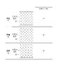
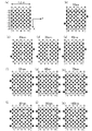
- FIGS. 9A to 9C are diagrams for explaining an example in which spot positions are arranged in a square in a rectangular area.
- FIGS. 9A to 9C are diagrams for explaining an example in which spot positions are arranged in a square in a rectangular area.
- FIGS. 10A to 10C are diagrams for explaining an example in which spot positions are staggered in a rectangular area.
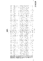
- FIG. 11 is a table showing an arrangement example of spot positions in zigzag exposure.
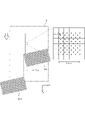
- FIG. 12 is a diagram for explaining zigzag exposure at a joint portion.
- 13A and 13B are diagrams for explaining an example in which two DMDs share exposure at a spliced portion.
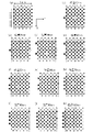
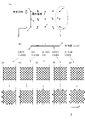
- FIGS. 14(a) to 14(k) are diagrams for explaining line pattern position correction.
- FIG. 15 is a graph showing the results of position measurement when line pattern position correction is performed by the method of FIGS. 14(a) to 14(k).
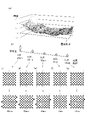
- FIGS. 16A to 16K are diagrams (part 1) for explaining the line width adjustment of the line pattern.
- FIGS. 17A to 17L are diagrams (part 2) for explaining line width adjustment of line patterns.
- FIG. 18 is a graph showing line width measurement results when the line width of the line pattern is adjusted by the method of FIGS. 16(a) to 17(l).
- FIGS. 19A to 19G are diagrams for explaining correction based on distortion measurement results.
- 20(a) to 20(g) are diagrams for explaining the correction based on the measurement result of the illuminance distribution.
- a pattern exposure apparatus (hereinafter simply referred to as an exposure apparatus) according to one embodiment will be described with reference to the drawings.
- FIG. 1 is a perspective view showing an overview of the external configuration of an exposure apparatus EX according to one embodiment.
- the exposure apparatus EX is an apparatus that forms and projects, onto a substrate to be exposed, exposure light whose intensity distribution in space is dynamically modulated by a spatial light modulator (SLM).
- SLM spatial light modulator
- Examples of spatial light modulators include liquid crystal devices, digital micromirror devices (DMDs), magneto-optical spatial light modulators (MOSLMs), and the like.
- the exposure apparatus EX according to this embodiment includes the DMD 10 as a spatial light modulator, but may include other spatial light modulators.
- the exposure apparatus EX is a step-and-scan projection exposure apparatus (scanner) that exposes a rectangular glass substrate used in a display device (flat panel display) or the like. be.
- the glass substrate is a flat panel display substrate P having at least one side length or diagonal length of 500 mm or more and a thickness of 1 mm or less.
- the exposure device EX exposes a photosensitive layer (photoresist) formed on the surface of the substrate P with a constant thickness to a projected image of a pattern created by the DMD.
- the substrate P unloaded from the exposure apparatus EX after exposure is sent to predetermined process steps (film formation step, etching step, plating step, etc.) after the development step.
- the exposure apparatus EX includes a pedestal 2 placed on active vibration isolation units 1a, 1b, 1c, and 1d (1d is not shown), a platen 3 placed on the pedestal 2, and An XY stage 4A that can move two-dimensionally, a substrate holder 4B that sucks and holds the substrate P on a plane on the XY stage 4A, and laser length measurement interference that measures the two-dimensional movement position of the substrate holder 4B (substrate P).
- a stage device comprising an interferometer (hereinafter simply referred to as an interferometer) IFX and IFY1 to IFY4 is provided.
- Such a stage apparatus is disclosed, for example, in US Patent Publication No. 2010/0018950 and US Patent Publication No. 2012/0057140.
- the XY plane of the orthogonal coordinate system XYZ is set parallel to the flat surface of the surface plate 3 of the stage device, and the XY stage 4A is set to be translatable within the XY plane.
- the direction parallel to the X-axis of the coordinate system XYZ is set as the scanning movement direction of the substrate P (XY stage 4A) during scanning exposure.
- the movement position of the substrate P in the X-axis direction is sequentially measured by the interferometer IFX, and the movement position in the Y-axis direction is sequentially measured by at least one (preferably two) of the four interferometers IFY1 to IFY4. be.
- the substrate holder 4B is configured to be slightly movable in the direction of the Z-axis perpendicular to the XY plane with respect to the XY stage 4A and to be slightly inclined in any direction with respect to the XY plane, and projected onto the surface of the substrate P. Focus adjustment and leveling (parallelism) adjustment with respect to the imaging plane of the pattern are actively performed. Further, the substrate holder 4B is configured to be slightly rotatable ( ⁇ z rotation) about an axis parallel to the Z axis in order to actively adjust the tilt of the substrate P within the XY plane.
- the exposure apparatus EX further includes an optical surface plate 5 that holds a plurality of exposure (drawing) modules MU(A), MU(B), and MU(C), and a main column 6a that supports the optical surface plate 5 from the pedestal 2. , 6b, 6c, 6d (6d not shown).
- Each of the plurality of exposure modules MU(A), MU(B), and MU(C) is attached to the +Z direction side of the optical platen 5 .
- the plurality of exposure modules MU(A), MU(B), and MU(C) may be attached individually to the optical surface plate 5, or the rigidity may be increased by connecting two or more exposure modules. It may be attached to the optical platen 5 in a state where it is stuck.
- Each of the plurality of exposure modules MU(A), MU(B), and MU(C) is attached to the +Z direction side of the optical surface plate 5, and an illumination unit ILU that receives illumination light from the optical fiber unit FBU; It has a projection unit PLU attached to the -Z direction side of the optical platen 5 and having an optical axis parallel to the Z axis. Furthermore, each of the exposure modules MU(A), MU(B), and MU(C) serves as a light modulating section that reflects the illumination light from the illumination unit ILU in the -Z direction and causes it to enter the projection unit PLU.
- a DMD 10 is provided. A detailed configuration of the exposure module including the illumination units ILU and DMD 10 and the projection unit PLU will be described later.
- a plurality of alignment systems (microscopes) ALG for detecting alignment marks formed at a plurality of predetermined positions on the substrate P are attached to the -Z direction side of the optical platen 5 of the exposure apparatus EX.
- a calibration reference unit CU for calibration is provided at the -X direction end on the substrate holder 4B. Calibration is performed by confirming (calibrating) the relative positional relationship within the XY plane of each detection field of alignment system ALG, and by performing projection unit Confirmation (calibration) of the baseline error between each projection position of the pattern image projected from the PLU and the position of each detection field of the alignment system ALG, and confirmation of the position and image quality of the pattern image projected from the projection unit PLU.
- the number of modules may be less than or more than nine.
- three rows of exposure modules are arranged in the X-axis direction, but the number of rows of exposure modules arranged in the X-axis direction may be two or less, or four or more. .
- FIG. 2 is a diagram showing an arrangement example of the projection areas IAn of the DMD 10 projected onto the substrate P by the projection units PLU of the exposure modules MU(A), MU(B), and MU(C).
- System XYZ is set the same as in FIG.
- the projection area IAn can be said to be the irradiation range (light irradiation area group) of the illumination light reflected by the plurality of micromirrors 10a of the DMD 10 and guided onto the substrate P by the projection unit PLU.
- each of the exposure modules MU (A) in the first row, the exposure modules MU (B) in the second row, and the exposure modules MU (C) in the third row, which are spaced apart in the X direction, It consists of nine modules arranged in the Y direction.
- the exposure module MU (A) is composed of nine modules MU1 to MU9 arranged in the +Y direction
- the exposure module MU (B) is composed of nine modules MU10 to MU18 arranged in the -Y direction
- the module MU(C) is composed of nine modules MU19 to MU27 arranged in the +Y direction.
- the modules MU1 to MU27 all have the same configuration, and when the exposure module MU(A) and the exposure module MU(B) face each other in the X direction, the exposure module MU(B) and the exposure module MU(C) are in a back-to-back relationship with respect to the X direction.
- the -Y direction ends of the projection areas IA1 to IA9 in the first row and the +Y directions of the projection areas IA10 to IA18 in the second row
- a splice exposure is performed at the ends of the direction. Areas on the substrate P that have not been exposed in the projection areas IA1 to IA18 in the first and second rows are successively exposed by the projection areas IA19 to IA27 in the third row.
- the center point of each of the projection areas IA1 to IA9 in the first row is located on a line k1 parallel to the Y axis
- the center point of each of the projection areas IA10 to IA18 in the second row is on a line k2 parallel to the Y axis
- the center point of each of the projection areas IA19 to IA27 in the third row is located on a line k3 parallel to the Y-axis.
- the distance in the X direction between the lines k1 and k2 is set to the distance XL1
- the distance in the X direction between the lines k2 and k3 is set to the distance XL2.
- the connecting portion between the -Y direction end of the projection area IA9 and the +Y direction end of the projection area IA10 is OLa
- the -Y direction end of the projection area IA10 and the +Y direction end of the projection area IA27 and OLb, and the joint portion between the +Y-direction end of the projection area IA8 and the -Y-direction end of the projection area IA27 is OLc.
- the orthogonal coordinate system XYZ is set the same as in FIGS.
- the coordinate system X'Y' in the projection areas IA8, IA9, IA10, IA27 (and all other projection areas IAn) is It is set to incline by an angle ⁇ k (0° ⁇ k ⁇ 90°) with respect to the X-axis and Y-axis (lines k1 to k3) of the orthogonal coordinate system XYZ. That is, the regions (light irradiation regions) on the substrate P onto which the illumination light reflected by the numerous micromirrors of the DMD 10 is projected are two-dimensionally arranged along the X'-axis and the Y'-axis.
- a circular area encompassing each of the projection areas IA8, IA9, IA10, IA27 (and all other projection areas IAn as well) in FIG. 3 represents the circular image field PLf' of the projection unit PLU.
- the projection image (light irradiation area) of the micromirrors arranged obliquely (angle ⁇ k) at the end of the projection area IA9 in the -Y' direction and the oblique (angle ⁇ k) end of the +Y' direction of the projection area IA10. .theta.k) are set so as to overlap the projection images (light irradiation areas) of the micromirrors.
- the projection image (light irradiation area) of the micromirrors arranged obliquely (angle ⁇ k) at the ⁇ Y′ direction end of the projection area IA10 and the oblique +Y′ direction end of the projection area IA27 It is set so as to overlap the projection image (light irradiation area) of the micromirrors arranged at (angle ⁇ k).
- the projection image (light irradiation area) of the micromirrors arranged obliquely (angle ⁇ k) at the +Y′ direction end of the projection area IA8 and the ⁇ Y′ direction end of the projection area IA27 are projected. It is set so as to overlap the projected image (light irradiation area) of the micromirrors arranged obliquely (angle ⁇ k).
- FIG. 4 is an optical layout diagram of the specific configuration of the module MU18 in the exposure module MU(B) and the module MU19 in the exposure module MU(C) shown in FIGS. 1 and 2, viewed in the XZ plane. is.
- the orthogonal coordinate system XYZ in FIG. 4 is set the same as the orthogonal coordinate system XYZ in FIGS.
- the module MU18 is shifted in the +Y direction with respect to the module MU19 by a constant interval and is installed in a back-to-back relationship.
- the optical fiber unit FBU shown in FIG. 1 is composed of 27 optical fiber bundles FB1 to FB27 corresponding to the 27 modules MU1 to MU27 shown in FIG.
- the illumination unit ILU of the module MU18 functions as a mirror 100 that reflects the illumination light ILm traveling in the -Z direction from the output end of the optical fiber bundle FB18, a mirror 102 that reflects the illumination light ILm from the mirror 100 in the -Z direction, and a collimator lens.
- Mirror 102, input lens system 104, optical integrator 108, condenser lens system 110, and tilt mirror 112 are arranged along optical axis AXc parallel to the Z axis.
- the optical fiber bundle FB18 is configured by bundling one optical fiber line or a plurality of optical fiber lines.
- the illumination light ILm emitted from the output end of the optical fiber bundle FB18 (each of the optical fiber lines) is set to a numerical aperture (NA, also called divergence angle) so as to enter the input lens system 104 at the subsequent stage without being vignetted.
- NA numerical aperture
- the position of the front focal point of the input lens system 104 is designed to be the same as the position of the output end of the optical fiber bundle FB18.
- the position of the rear focal point of the input lens system 104 is such that the illumination light ILm from a single or a plurality of point light sources formed at the output end of the optical fiber bundle FB18 is superimposed on the incident surface side of the MFE lens 108A of the optical integrator 108. is set to let Therefore, the incident surface of the MFE lens 108A is Koehler-illuminated by the illumination light ILm from the exit end of the optical fiber bundle FB18.
- the geometric center point in the XY plane of the output end of the optical fiber bundle FB18 is positioned on the optical axis AXc, and the principal ray ( center line) is parallel (or coaxial) with the optical axis AXc.
- Illumination light ILm from input lens system 104 is attenuated by an arbitrary value in the range of 0% to 90% by illumination adjustment filter 106, and then passes through optical integrator 108 (MFE lens 108A, field lens, etc.). , enter the condenser lens system 110 .
- the MFE lens 108A is a two-dimensional arrangement of a large number of rectangular microlenses of several tens of ⁇ m square. ) is set to be almost similar to Also, the position of the front focal point of the condenser lens system 110 is set to be substantially the same as the position of the exit surface of the MFE lens 108A.
- each illumination light from a point light source formed on each exit side of a large number of microlenses of the MFE lens 108A is converted into a substantially parallel light beam by the condenser lens system 110, and after being reflected by the tilt mirror 112, , are superimposed on the DMD 10 to form a uniform illuminance distribution. Since a surface light source in which a large number of point light sources (condensing points) are two-dimensionally densely arranged is generated on the exit surface of the MFE lens 108A, the MFE lens 108A functions as a surface light source forming member.
- the optical axis AXc passing through the condenser lens system 110 and parallel to the Z-axis is bent by the tilt mirror 112 and reaches the DMD 10.
- AXb the neutral plane including the center point of each of the numerous micromirrors of the DMD 10 is set parallel to the XY plane. Therefore, the angle formed by the normal to the neutral plane (parallel to the Z-axis) and the optical axis AXb is the incident angle ⁇ of the illumination light ILm with respect to the DMD 10 .
- the DMD 10 is attached to the underside of a mount portion 10M fixed to the support column of the illumination unit ILU.
- the mount section 10M is provided with a fine movement stage that combines a parallel link mechanism and an extendable piezo element as disclosed in, for example, International Publication No. 2006/120927. be done.
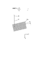
- FIG. 5(a) is a diagram schematically showing the DMD 10
- FIG. 5(b) is a diagram showing the DMD 10 when the power is off
- FIG. 5(c) is an explanation of mirrors in the ON state
- FIG. 5D is a diagram for explaining the mirror in the OFF state.
- mirrors in the ON state are indicated by hatching.
- the DMD 10 has a plurality of micromirrors 10a whose reflection angle can be changed and controlled.
- the DMD 10 is of a roll-and-pitch drive type in which the ON state and the OFF state are switched by tilting in the roll direction and tilting in the pitch direction of the micromirror 10a.
- each micromirror 10a when the power is off, the reflecting surface of each micromirror 10a is set parallel to the X'Y' plane.
- the arrangement pitch of the micromirrors 10a in the X' direction is Pdx ([mu]m), and the arrangement pitch in the Y' direction is Pdy ([mu]m).
- Each micromirror 10a is turned on by tilting around the Y'-axis.
- FIG. 5(c) shows a case where only the central micromirror 10a is in the ON state and the other micromirrors 10a are in the neutral state (neither ON nor OFF state).
- Each micromirror 10a is turned off by tilting around the X' axis.
- FIG. 5(d) shows a case where only the central micromirror 10a is in the OFF state and the other micromirrors 10a are in the neutral state.
- the ON-state micromirror 10a is arranged from the X'Y' plane so that the illumination light applied to the ON-state micromirror 10a is reflected in the X direction of the XZ plane. It is driven to tilt at a predetermined angle. Further, the micromirror 10a in the OFF state is driven to be inclined at a predetermined angle from the X'Y' plane so that the illumination light irradiated to the micromirror 10a in the ON state is reflected in the Y direction in the YZ plane. .
- the DMD 10 generates an exposure pattern by switching the ON state and OFF state of each micromirror 10a.
- Illumination light reflected by the mirror in the OFF state is absorbed by a light absorber (not shown).
- the DMD 10 has been described as an example of a spatial light modulator, the DMD 10 has been described as a reflective type that reflects laser light. A diffractive type may also be used.
- a spatial light modulator can spatially and temporally modulate laser light.
- the illumination light ILm irradiated to the ON-state micromirror 10a of the micromirrors 10a of the DMD 10 is reflected in the X direction in the XZ plane toward the projection unit PLU.
- the illumination light ILm irradiated to the OFF-state micromirror 10a among the micromirrors 10a of the DMD 10 is reflected in the Y direction in the YZ plane so as not to face the projection unit PLU.
- a movable shutter 114 for shielding reflected light from the DMD 10 during a non-exposure period is detachably provided in the optical path between the DMD 10 and the projection unit PLU.
- the movable shutter 114 is rotated to an angular position retracted from the optical path during the exposure period, as illustrated on the module MU19 side, and inserted obliquely into the optical path during the non-exposure period, as illustrated on the module MU18 side. is rotated to the desired angular position.
- a reflecting surface is formed on the DMD 10 side of the movable shutter 114 , and the light from the DMD 10 reflected there is applied to the light absorber 117 .
- the light absorber 117 absorbs light energy in the ultraviolet wavelength range (wavelength of 400 nm or less) without re-reflection and converts it into heat energy. Therefore, the light absorber 117 is also provided with a heat dissipation mechanism (radiating fins or a cooling mechanism). Although not shown in FIG. 4, the reflected light from the micromirror 10a of the DMD 10, which is in the OFF state during the exposure period, is reflected in the Y direction ( 4) is absorbed by a similar light absorber (not shown in FIG. 4).
- the projection unit PLU attached to the lower side of the optical surface plate 5 is a double-telecentric combination composed of a first lens group 116 and a second lens group 118 arranged along an optical axis AXa parallel to the Z axis. It is configured as an image projection lens system.
- the first lens group 116 and the second lens group 118 are translated in the direction along the Z-axis (optical axis AXa) by a fine actuator with respect to a support column fixed to the lower side of the optical surface plate 5.
- the projection magnification Mp is set to approximately 1/6 in consideration of the tilt angle ⁇ k at .
- An imaging projection lens system consisting of lens groups 116 and 118 inverts/inverts the reduced image of the entire mirror surface of the DMD 10 and forms an image on a projection area IA18 (IAn) on the substrate P.
- the first lens group 116 of the projection unit PLU can be finely moved in the direction of the optical axis AXa by an actuator in order to finely adjust the projection magnification Mp (approximately ⁇ several tens of ppm), and the second lens group 118 is for high-speed focus adjustment. Therefore, the actuator can be finely moved in the direction of the optical axis AXa. Further, a plurality of oblique incident light type focus sensors 120 are provided below the optical surface plate 5 in order to measure the positional change of the surface of the substrate P in the Z-axis direction with submicron accuracy.
- the projection area IAn must be tilted by the angle ⁇ k in the XY plane as described above with reference to FIG. (at least the optical path portion of the mirrors 102 to 112 along the optical axis AXc) are arranged so as to be inclined by an angle ⁇ k in the XY plane as a whole.
- a light beam (that is, a spatially modulated light beam) formed only by reflected light from the micromirror 10a in the ON state among the micromirrors 10a of the DMD 10 is projected onto the micromirror 10a via the projection unit PLU.
- area on the substrate P that is optically conjugate In the following description, a region on the substrate P that is conjugate with each micromirror 10a is called a light-irradiated region, and a group of light-irradiated regions is called a light-irradiated region group.
- the projection area IAn matches the light irradiation area group. That is, the light-irradiated region group on the substrate P has a large number of light-irradiated regions arranged in two-dimensional directions (X' direction and Y' direction).
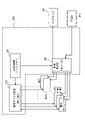
- FIG. 6 is a functional block diagram showing the functional configuration of the exposure control device 300 included in the exposure apparatus EX according to this embodiment.
- the exposure control device 300 includes a drawing data storage unit 310 , a control data creation unit 301 , a drive control unit 304 and an exposure control unit 306 .
- the drawing data storage unit 310 sends drawing data MD1 to MD27 for pattern exposure to the DMDs 10 of the 27 modules MU1 to MU27 shown in FIG.
- the drive control unit 304 creates control data CD1 to CD27 based on the measurement results of the interferometer IFX, and sends them to the modules MU1 to MU27. Further, the drive control unit 304 scans the XY stage 4A in the scanning direction (X-axis direction) at a predetermined speed based on the measurement result of the interferometer IFX.
- the modules MU1 to MU27 control the driving of the micromirror 10a of the DMD 10 based on the drawing data MD1 to MD27 and the control data CD1 to CD27 sent from the drive control section 304 during scanning exposure.
- the control data CD1 to CD27 are reset pulses.
- Each micromirror 10a assumes a predetermined posture according to the drawing data MD1 to MD27 upon receiving the reset pulse. At this time, each micromirror 10a changes its posture corresponding to the number of times the reset pulse is received each time the reset pulse is received.
- the exposure control unit (sequencer) 306 transmits the drawing data MD1 to MD27 from the drawing data storage unit 310 to the modules MU1 to MU27 in synchronization with the scanning exposure (moving position) of the substrate P, control data CD1 to CD27 (reset pulse).
- FIG. 7 is a diagram schematically showing the projection area (light irradiation area group) IAn and the exposure target area (area where the line pattern is exposed) 30 on the substrate P.
- the exposure target area 30 is scanned with respect to the projection area (light irradiation area group) IAn, and the DMD 10 detects the center of the light irradiation area 32 included in the projection area (light irradiation area group) IAn. ) is positioned within the exposure target region 30, the micromirror 10a corresponding to the light irradiation region 32 is turned on.
- This rectangular area 34 is, for example, a square area with a side of 1 ⁇ m. It is also assumed that the light irradiation area 32 corresponding to each micromirror 10a is also a square area with a side of 1 ⁇ m.
- the DMD 10 receives a reset pulse from the drive control unit 304 at the timing when the rectangular area 34 is at the position 34A to turn on the micromirror corresponding to the light irradiation area 210a. , such that when DMD 10 receives the next reset pulse to turn on the micromirror corresponding to illuminated area 210c, rectangular area 34 is positioned at position 34C. In this case, the rectangular area 34 will move by the free running distance shown in FIG. 8 between the reset pulses. That is, the free running distance is the distance between the rectangular area 34 located at the position 34A and the rectangular area 34 located at the position 34C.
- FIG.9(b) is the figure which abbreviate
- the rectangular area 34 is exposed in this manner, the rectangular area 34 is exposed with 26 pulses so that the spot positions are positioned in a 6 ⁇ 6 square arrangement (so that the spot positions are positioned on grid points arranged in the XY directions). will be exposed.
- the distance between adjacent spot positions in the X-axis direction and the Y-axis direction is 0.2 ⁇ m.
- the DMD 10 receives a reset pulse from the drive control unit 304 at the timing when the rectangular area 34 is at the position 34D, and turns on the micromirror corresponding to the light irradiation area 210d. , such that when DMD 10 receives the next reset pulse to turn on the micromirror corresponding to illuminated area 210f, rectangular area 34 will be at position 34F. In this case, the rectangular area 34 moves by the free running distance +1/5 ( ⁇ m) shown in FIG. 8 between the reset pulses.
- the center position of the rectangular area 34 and the center position of the light irradiation area 210e match.
- the center position of the rectangular region 34 at the position 34D and the center position of the light irradiation region 210d match. Therefore, omitting the free running distance, the positional relationship between the rectangular area 34 and the light irradiation area group when the substrate P is scanned at the second scanning speed can be represented as shown in FIG. 10(a).
- 10A shows the position of the rectangular area 34 each time the DMD 10 receives the reset pulse to change the state of the micromirror 10a, and the light irradiation area 32 corresponding to the micromirror 10a that exposes the rectangular area 34.
- FIG.10(b) is the figure which abbreviate
- the rectangular area 34 is exposed in this way, the rectangular area 34 is exposed with 18 spot positions arranged (in a staggered arrangement) with 14 pulses as shown in FIG. 10(c).
- the distance between adjacent spot positions in the X-axis direction and the Y-axis direction is 0.2 ⁇ m.
- the zigzag arrangement enables exposure with the same resolution as in the case of the square arrangement.
- the scanning speed of the substrate P can be increased, and a high throughput can be achieved. Therefore, in this embodiment, ⁇ k and the scanning speed of the substrate P are determined so that the spot positions are arranged in a staggered manner as shown in FIG. 10(c).
- exposure such as that shown in FIG. 10C is referred to as zigzag exposure.
- the spot positions can be positioned at the four corners of the rectangular area 34 .
- an arrangement in which the spot positions are not positioned at the four corners of the rectangular area 34 may be employed.
- each spot position can be located inside the rectangular area 34 as in arrangement (3).
- the required number of pulses is 61 in arrangements (1) and (2), whereas the required number of pulses can be 50 in arrangement (3). Therefore, one of the arrangements (1), (2) and (3) can be selected according to the sensitivity of the resist applied on the substrate P, for example.
- FIG. 12 is a diagram schematically showing a state in which a line pattern is exposed at a joint portion (for example, joint portion OLa).
- a joint portion for example, joint portion OLa
- the inside of the rectangular area 34 is zigzag exposed.
- the line pattern may be exposed using only one DMD.
- the portions that can be exposed by one DMD may be exposed, and the remaining portions may be exposed by the other DMD.
- the number of exposure pulses may be shared substantially evenly for each of the two DMDs.
- the locations (spot positions) to be exposed using each DMD may be set randomly, or as shown by “black circles ( ⁇ )” and “white circles ( ⁇ )” in FIG.
- the ratio of exposed portions may gradually increase or decrease in the non-scanning direction (Y-axis direction) or the scanning direction.
- FIG. 12 describes the case where the joint portion is a portion to be exposed using two DMDs, but it is not limited to this.
- a joint portion is a portion where the projection area of the DMD passes through twice in succession. Also when exposing this joint portion, zigzag exposure can be performed as described above.
- spot position indicated by a white circle near the center of the spot row on the right end, as shown in FIG.
- spot position indicated by a double black circle is added to the left.
- the line pattern when the line pattern is shifted leftward by 10 nm, as shown in FIG. position) to the left.
- the line pattern can be shifted by eliminating/adding spot locations on or near the edges of the line pattern rather than eliminating/adding spot locations at or near the center of the line pattern. quantity can be increased.
- FIGS. By changing the combination of adding a new spot on the left side and deleting (or not deleting) a part of the spot position that originally existed in this way, FIGS. As shown in 14(k), the line pattern can be shifted to the left by 10 nm, 20 nm, .
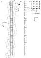
- FIG. 15 shows the position measurement results when line pattern position correction is performed by the method of FIGS. 14(a) to 14(k). In this position measurement, how much the position of the line pattern was corrected (shifted) in the Y-axis direction was measured at 11 points in the X-axis direction indicated by arrows in FIG. 14(a). From FIG. 15, it can be seen that the position of the line pattern can be corrected to approximately the desired position at any position in the X-axis direction.
- the ON/OFF state of the micromirror 10a of the DMD 10 is controlled so that zigzag exposure is performed. Thereby, a pattern can be exposed at a desired position.
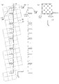
- one new spot position (double black circle) is placed on both sides of the reference pattern in FIG. 16(a), and two spot positions in the reference pattern are deleted. (white circle), the line width can be increased by 10 nm. Further, when increasing the line width by 20 nm, as shown in FIG. Two spot positions different from those in FIG. 16(b) may be deleted.
- the line width can be adjusted by a combination of arranging the same number of new spot positions on both sides of the reference pattern and deleting (or not deleting) some of the spot positions of the reference pattern.
- FIG. 18 shows the measurement results of the line width when the line width of the line pattern is adjusted by the method of FIGS. 16(a) to 17(l).
- the line width (width in the Y-axis direction) of the line pattern was measured at 11 points in the X-axis direction indicated by arrows in FIG. 16(a). From FIG. 18, it can be seen that the line width of the line pattern could be adjusted to approximately the desired line width at any position in the X-axis direction.
- the line width of the line pattern is to be adjusted by a size equal to or less than the staggered grid interval (the interval between the spot positions in the X and Y directions), the line width shown in FIGS.
- the ON/OFF state of the micromirror 10a of the DMD 10 is controlled so that such exposure is performed. Thereby, a desired line pattern can be obtained with high accuracy.
- FIG. 19A shows an example of measurement results of distortion of a projected image of a module included in the exposure module by test exposure or the like. Arrows at each point indicate the direction and magnitude of distortion. Distortion measurement involves exposing the substrate P using a test pattern (test exposure), detecting an image (transfer image) exposed on the substrate P, and obtaining image distortion data (distortion data) using the detection results. Including creation.
- the average value of the distortion at points in the same non-scanning direction is calculated.
- An example of the calculation result of the average value of distortion for each non-scanning direction is shown in FIG. 19(b).
- the spot position for exposing a square area is devised for each position in the non-scanning direction. For example, when the average value of distortion in the X direction is 0.05 ⁇ m and in the Y direction is ⁇ 0.06 ⁇ m as shown on the left end of FIG. Three new spot positions (double black circles) are arranged on the left side and the bottom side of the zigzag exposure pattern (reference pattern), and five spot positions of the original square pattern are deleted.
- the spot position may be changed according to the average value of the distortion, as shown in FIGS. 19(d) to 19(g).
- the influence of distortion on exposure accuracy can be suppressed.
- the processing can be simplified. Also, by using the average value of distortion for each non-scanning direction, it is possible to prevent, for example, a pattern extending in the scanning direction from being exposed in a jagged shape.
- FIG. 20(a) shows an example of the measurement result of the illuminance distribution in one exposure area.
- the following exposure is performed in order to suppress the influence of the illuminance distribution.
- FIG. 20B shows an example of the calculation result of the average value of illuminance for each non-scanning direction.
- FIG. 20(b) it is assumed that from the left, 1.0%, 0.4%, 0.2%, 0.0%, and 0.3% are calculated.
- the line width becomes narrower by 50 nm when the illuminance increases by 1.0% from the condition of the photoresist, and the exposure is performed so that the line width increases as the illuminance increases.
- the method of widening the line width is the same as in FIGS. 16(b) to 17(l).
- the spot position is changed from the reference pattern according to the illuminance, as shown in FIGS. 20(d) to 20(g).
- the influence of the illuminance distribution on the exposure accuracy can be suppressed.
- the average value of the illuminance for each non-scanning direction is calculated and used for processing, so the processing can be simplified. Further, by using the average value of the illuminance for each non-scanning direction, it is possible to prevent, for example, a pattern extending in the scanning direction from being exposed in a jagged shape.
- the substrate holder 4B that holds and moves the substrate P, the exposure modules MU(A), MU(B), and MU(C) that have the DMDs 10, the substrate and a drive control unit 304 that drives the holder 4B in the scanning direction.
- the arrangement direction (X′ axis, Y′ axis) of the light irradiation regions in the light irradiation region group of the exposure module is inclined by an angle ⁇ k with respect to the scanning direction and the non-scanning direction.
- the substrate holder 4B is scanned at a speed such that when the predetermined range of P is exposed, the exposure is staggered (spot positions are arranged in a staggered manner).
- the DMD 10 has a finite number of micromirrors 10a in the scanning direction, but by exposing the pattern with a small number of pulses, it is possible to increase the possibility of exposing the desired pattern during one scan.
- the speed of the stage can be increased, and the throughput of the exposure apparatus can be improved.
- zigzag exposure is performed even when exposing the joint portion using two DMDs 10, so that the joint portion can be exposed with the same pattern as that for the portion other than the joint portion.
- the DMD 10 when exposure is to be performed by shifting the line pattern by a distance smaller than the grid interval, part of the spot positions in the line pattern before being shifted is exposed outside the line pattern (outside of the direction in which the shift is desired).
- the DMD 10 is driven so as to As a result, the line pattern can be easily exposed by being shifted by a distance smaller than the grid interval.
- the same number of new spot positions are arranged on both sides of the original line pattern (reference pattern), and the original line Drive the DMD 10 to reduce (or not reduce) the spot positions of the pattern.
- the line width of the line pattern can be easily exposed by a dimension smaller than the grid interval.
- the spot position of the line pattern is changed based on the distortion of the module and the illuminance distribution so that the influence of the distortion and the illuminance distribution is suppressed. This makes it possible to easily suppress the influence of distortion and illuminance distribution on exposure accuracy.
- NA and ⁇ are made variable
- illumination conditions are made variable
- OPC Optical Proximity Correction
Landscapes
- Physics & Mathematics (AREA)
- General Physics & Mathematics (AREA)
- Optics & Photonics (AREA)
- Exposure And Positioning Against Photoresist Photosensitive Materials (AREA)
- Exposure Of Semiconductors, Excluding Electron Or Ion Beam Exposure (AREA)
Abstract
Description
図1は、一実施形態に係る露光装置EXの外観構成の概要を示す斜視図である。露光装置EXは、空間光変調素子(SLM:Spatial Light Modulator)によって、空間内での強度分布が動的に変調される露光光を被露光基板に結像投影する装置である。空間光変調器の例としては、液晶素子、デジタルマイクロミラーデバイス(DMD:Digital Micromirror Device)、磁気光学空間光変調器(MOSLM:Magneto Optic Spatial Light Modulator)等が挙げられる。本実施形態に係る露光装置EXは、空間光変調器としてDMD10を備えるが、他の空間光変調器を備えていてもよい。
図4は、図1、図2に示した露光モジュールMU(B)中のモジュールMU18と、露光モジュールMU(C)中のモジュールMU19との具体的な構成をXZ面内で見た光学配置図である。図4の直交座標系XYZは図1~図3の直交座標系XYZと同じに設定される。また、図2に示した各モジュールのXY面内での配置から明らかなように、モジュールMU18はモジュールMU19に対して+Y方向に一定間隔だけずらされると共に、互いに背中合わせの関係で設置されている。モジュールMU18内の各光学部材とモジュールMU19内の各光学部材は、それぞれ同じ材料で同じに構成されるので、ここでは主にモジュールMU18の光学構成について詳細に説明する。なお、図1に示した光ファイバーユニットFBUは、図2に示した27個のモジュールMU1~MU27の各々に対応して、27本の光ファイバー束FB1~FB27で構成される。
図5(a)は、DMD10を概略的に示す図であり、図5(b)は、電源がOFFの場合のDMD10を示す図であり、図5(c)は、ON状態のミラーについて説明するための図であり、図5(d)は、OFF状態のミラーについて説明するための図である。なお、図5(a)~図5(d)において、ON状態にあるミラーをハッチングで示している。
光学定盤5の下側に取り付けられた投影ユニットPLUは、Z軸と平行な光軸AXaに沿って配置される第1レンズ群116と第2レンズ群118とで構成される両側テレセントリックな結像投影レンズ系として構成される。第1レンズ群116と第2レンズ群118は、それぞれ光学定盤5の下側に固設される支持コラムに対して、Z軸(光軸AXa)に沿った方向に微動アクチュエータで並進移動するように構成される。第1レンズ群116と第2レンズ群118による結像投影レンズ系の投影倍率Mpは、DMD10上のマイクロミラーの配列ピッチPdと、基板P上の投影領域IAn(n=1~27)内に投影されるパターンの最小線幅(最小画素寸法)Pgとの関係で決められる。
上記構成を有する露光装置EXにおいて行われる、走査露光処理を含む各種処理は、露光制御装置300によって制御される。図6は、本実施形態に係る露光装置EXが備える露光制御装置300の機能構成を示す機能ブロック図である。
図7は、投影領域(光照射領域群)IAnと、基板P上の露光対象領域(ラインパターンを露光する領域)30とを模式的に示す図である。本実施形態では、露光対象領域30が投影領域(光照射領域群)IAnに対して走査され、DMD10は、投影領域(光照射領域群)IAnに含まれる光照射領域32の中心(スポット位置と呼ぶ)が露光対象領域30内に位置するタイミングで、当該光照射領域32に対応するマイクロミラー10aをON状態にする。
第1の走査速度は、図8に示すように、矩形領域34が位置34AにあるタイミングでDMD10が駆動制御部304からリセットパルスを受信して光照射領域210aに対応するマイクロミラーをオン状態とし、DMD10が次のリセットパルスを受信して光照射領域210cに対応するマイクロミラーをオン状態とするときに矩形領域34が位置34Cに位置するような速度である。この場合、矩形領域34は、リセットパルス間において、図8に示す空走距離だけ移動することになる。つまり、空走距離とは、位置34Aに位置する矩形領域34と、位置34Cに位置する矩形領域34の間の距離である。
第2の走査速度は、図8に示すように、矩形領域34が位置34DにあるタイミングでDMD10が駆動制御部304からリセットパルスを受信して光照射領域210dに対応するマイクロミラーをオン状態とし、DMD10が次のリセットパルスを受信して光照射領域210fに対応するマイクロミラーをオン状態とするときに矩形領域34が位置34Fに位置するような速度である。この場合、矩形領域34は、リセットパルス間において図8に示す空走距離+1/5(μm)だけ移動することになる。
図12は、継ぎ部(例えば継ぎ部OLa)においてラインパターンを露光する状態を模式的に示す図である。図12に示すように、継ぎ部OLaにおいてラインパターンを露光する場合にも、本実施形態では、矩形領域34内を千鳥露光する。この場合、継ぎ部OLaを露光する一方のDMD(例えば投影領域IA10に対応するDMD)でラインパターン全体を露光できる場合には、一方のDMDのみを用いてラインパターンを露光してもよい。また、両方のDMDを用いなければラインパターンを露光できない場合には、一方のDMDで露光できる箇所は露光し、残りの箇所を他方のDMDで露光することとしてもよい。また、2つのDMDそれぞれに対して露光パルス数を略均等に分担してもよい。この場合、各DMDを用いて露光する箇所(スポット位置)をランダムに設定しても良いし、図13において「黒丸(●)」と「白丸(○)」で示すように、一方のDMDが露光する箇所の割合が、非走査方向(Y軸方向)や走査方向に関して徐々に増減するようにしてもよい。
図14(a)に示すように1μm幅のラインパターンをグリッドが0.1μm間隔である千鳥ショットで実現する場合において、10nm(=0.01μm)単位でラインパターンの非走査方向に関する位置を補正する方法について説明する。
図16(a)に示すように、1μm幅のラインパターンを隣接するスポット位置の間隔(X軸及びY軸方向の間隔)が0.1μmである千鳥配置で実現する場合において、10nm(=0.01μm)単位でラインパターンの非走査方向(Y軸方向)に関する幅(線幅)を調整する方法について説明する。本実施形態では、図16(a)に示す元のラインパターン(基準パターンと呼ぶ)の両外側の隣接する位置に同数の新たなスポット位置を配置することと、基準パターンの一部のスポット位置を削除する(又は削除しない)ことと、の組み合わせにより、線幅を調整する。
図19(a)には、テスト露光等によって露光モジュールに含まれるモジュールの投影像の歪み(ディストーション)を測定した結果の一例が示されている。各点において示す矢印は、ディストーションの方向と大きさを示す。ディストーションの測定は、テストパターンを用いた基板Pの露光(テスト露光)、基板P上に露光された像(転写像)の検出、及びその検出結果を用いた像歪みデータ(ディストーション・データ)の作成を含む。
図20(a)には、1つの露光領域における照度分布の測定結果の一例が示されている。
10 DMD
10a マイクロミラー
304 駆動制御部
EX 露光装置
P 基板
Claims (10)
- 基板を保持して移動する基板ホルダと、
2次元配列された光変調素子を有する空間光変調器と、前記空間光変調器に照明光を照射する照明ユニットと、前記基板上において第1方向及び前記第1方向に垂直な第2方向に2次元配列された光照射領域群のそれぞれへと前記光変調素子からの前記照明光を導く投影ユニットと、を含むモジュールと、
前記基板ホルダを走査方向に駆動する制御部と、を備え、
前記光変調素子は、前記走査方向及び該走査方向に直交する非走査方向に対して所定角度θ(0°<θ<90°)傾斜し2次元配列され、
前記制御部は、前記基板の所定範囲を露光する際に、前記所定範囲内に照射される前記光変調素子それぞれから出射される前記照明光の中心を示すスポット位置が千鳥配置となるような速度で、前記基板ホルダを走査する、露光装置。 - 前記モジュールを複数備え、
前記制御部は、前記複数のモジュールのうちの第1のモジュールと、前記第1のモジュールに隣接する第2のモジュールと、を用いて露光できる第1範囲を露光する際に、前記第1範囲内の前記スポット位置の配置が千鳥配置となるような速度で、前記基板ホルダを走査する、請求項1に記載の露光装置。 - 前記モジュールは、前記第1のモジュールと、前記第2のモジュールとの両方のモジュールにより、前記第1範囲を露光する、請求項2に記載の露光装置。
- 前記千鳥配置となるように前記所定範囲を露光することと、前記走査方向及び前記非走査方向に並ぶ格子点上に前記スポット位置が配置される正方配置となるように前記所定範囲を露光することと、前記所定範囲の内側に前記スポット位置が千鳥配置される内側千鳥配置となるように前記所定範囲を露光することと、のいずれかの選択を受け付ける受付部を備える請求項1~3のいずれか一項に記載の露光装置。
- 前記所定範囲内を露光するときの前記スポット位置の一部を、前記所定範囲の外側の前記非走査方向に隣接する箇所に位置するように変更した描画データを用いて前記空間光変調器を駆動することで、前記所定範囲から前記非走査方向にずれた範囲を露光する、請求項1~4のいずれか一項に記載の露光装置。
- 前記所定範囲内を露光するときの前記スポット位置の一部を減らす又は減らさず、前記所定範囲の前記非走査方向の両側に隣接する箇所に新たなスポット位置を追加するように変更した描画データを用いて前記空間光変調器を駆動することで、前記所定範囲よりも前記非走査方向に幅が広い範囲を露光する、請求項1~4のいずれか一項に記載の露光装置。
- 前記モジュールによる投影像の歪みの測定結果に基づいて、前記投影像の歪みがない状態で前記所定範囲内を露光するときの前記スポット位置の一部を減らす又は減らさず、前記所定範囲の外側の前記非走査方向に隣接する箇所に新たなスポット位置を追加するように変更した描画データを生成し、生成した前記描画データを用いて前記空間光変調器を駆動することで、前記所定範囲を露光する、請求項1~4のいずれか一項に記載の露光装置。
- 前記投影像の歪みを2次元面内の複数箇所で測定し、前記非走査方向に関する位置が一致する箇所の平均に基づいて、前記非走査方向の各位置に対応する描画データを生成する、請求項7に記載の露光装置。
- 前記モジュールの照明分布の測定結果に基づいて、前記照明分布が理想的な状態で前記所定範囲内を露光するときの前記スポット位置の一部を減らす又は減らさず、前記所定範囲の前記非走査方向の両側に隣接する箇所に新たなスポット位置を追加するように変更した描画データを生成し、生成した前記描画データを用いて前記空間光変調器を駆動することで、前記所定範囲を露光する、請求項1~4のいずれか一項に記載の露光装置。
- 前記所定角度θは、tanθ=1/AのAの値が5,7,9,11となる角度である、請求項1~9のいずれか一項に記載の露光装置。
Priority Applications (6)
| Application Number | Priority Date | Filing Date | Title |
|---|---|---|---|
| JP2023533578A JP7548441B2 (ja) | 2021-07-05 | 2022-06-30 | 露光装置、制御方法、及びデバイス製造方法 |
| CN202280047560.5A CN117616341A (zh) | 2021-07-05 | 2022-06-30 | 曝光装置 |
| KR1020237045134A KR20240014513A (ko) | 2021-07-05 | 2022-06-30 | 노광 장치, 제어 방법, 및 디바이스 제조 방법 |
| US18/542,169 US20240126178A1 (en) | 2021-07-05 | 2023-12-15 | Exposure apparatus, control method, and device manufacturing method |
| JP2024135316A JP7845422B2 (ja) | 2021-07-05 | 2024-08-14 | 露光装置及び制御装置 |
| JP2026047164A JP2026091928A (ja) | 2021-07-05 | 2026-03-23 | 制御方法及びデバイス製造方法 |
Applications Claiming Priority (2)
| Application Number | Priority Date | Filing Date | Title |
|---|---|---|---|
| JP2021111804 | 2021-07-05 | ||
| JP2021-111804 | 2021-07-05 |
Related Child Applications (1)
| Application Number | Title | Priority Date | Filing Date |
|---|---|---|---|
| US18/542,169 Continuation US20240126178A1 (en) | 2021-07-05 | 2023-12-15 | Exposure apparatus, control method, and device manufacturing method |
Publications (1)
| Publication Number | Publication Date |
|---|---|
| WO2023282168A1 true WO2023282168A1 (ja) | 2023-01-12 |
Family
ID=84801597
Family Applications (1)
| Application Number | Title | Priority Date | Filing Date |
|---|---|---|---|
| PCT/JP2022/026201 Ceased WO2023282168A1 (ja) | 2021-07-05 | 2022-06-30 | 露光装置 |
Country Status (6)
| Country | Link |
|---|---|
| US (1) | US20240126178A1 (ja) |
| JP (3) | JP7548441B2 (ja) |
| KR (1) | KR20240014513A (ja) |
| CN (1) | CN117616341A (ja) |
| TW (1) | TW202318107A (ja) |
| WO (1) | WO2023282168A1 (ja) |
Citations (6)
| Publication number | Priority date | Publication date | Assignee | Title |
|---|---|---|---|---|
| JP2002367900A (ja) * | 2001-06-12 | 2002-12-20 | Yaskawa Electric Corp | 露光装置および露光方法 |
| JP2003332221A (ja) * | 2002-05-16 | 2003-11-21 | Dainippon Screen Mfg Co Ltd | 露光装置 |
| JP2004146789A (ja) * | 2002-08-29 | 2004-05-20 | Pentax Corp | パターン描画装置およびパターン描画方法 |
| JP2007033973A (ja) * | 2005-07-28 | 2007-02-08 | Fujifilm Corp | 露光ヘッドおよび露光装置 |
| JP2007318069A (ja) * | 2005-12-06 | 2007-12-06 | Nikon Corp | 露光装置及び露光方法、並びにデバイス製造方法、投影光学系 |
| JP2008065094A (ja) * | 2006-09-08 | 2008-03-21 | Fujifilm Corp | 描画用処理回路及び描画方法 |
Family Cites Families (13)
| Publication number | Priority date | Publication date | Assignee | Title |
|---|---|---|---|---|
| DE19522936C2 (de) * | 1995-06-23 | 1999-01-07 | Fraunhofer Ges Forschung | Vorrichtung zum Strukturieren einer photolithographischen Schicht |
| SE0104238D0 (sv) * | 2001-12-14 | 2001-12-14 | Micronic Laser Systems Ab | Method and apparatus for patterning a workpiece |
| JP4647355B2 (ja) * | 2004-03-29 | 2011-03-09 | 富士フイルム株式会社 | マルチビーム露光方法及び装置 |
| JP2007003830A (ja) * | 2005-06-23 | 2007-01-11 | Fujifilm Holdings Corp | フレームデータ作成装置及び方法並びにプログラム、描画装置 |
| US20100141732A1 (en) * | 2005-07-25 | 2010-06-10 | Fujifilm Corporation | Image recording device and method |
| JP5253916B2 (ja) * | 2008-03-10 | 2013-07-31 | 株式会社ジャパンディスプレイイースト | マスクレス露光方法 |
| KR100978118B1 (ko) * | 2008-05-06 | 2010-08-26 | 주식회사 이오테크닉스 | 초분해능 디지털 리소그래피 |
| JP6013097B2 (ja) * | 2012-09-14 | 2016-10-25 | 株式会社Screenホールディングス | パターン描画装置、パターン描画方法 |
| CN106062752B (zh) * | 2014-03-10 | 2020-03-17 | 应用材料公司 | 用于多带电粒子束平板印刷术的像素融合 |
| CN111512233B (zh) * | 2017-09-08 | 2023-03-28 | 株式会社尼康 | 图案描绘装置 |
| JP6652618B2 (ja) | 2018-10-11 | 2020-02-26 | 株式会社アドテックエンジニアリング | 照度割合変更方法及び露光方法 |
| JP7206830B2 (ja) * | 2018-11-15 | 2023-01-18 | 大日本印刷株式会社 | 荷電マルチビーム描画装置の描画データ作成方法 |
| CN110456612A (zh) * | 2019-07-02 | 2019-11-15 | 苏州源卓光电科技有限公司 | 一种高效率投影光刻成像系统及曝光方法 |
-
2022
- 2022-06-30 KR KR1020237045134A patent/KR20240014513A/ko active Pending
- 2022-06-30 WO PCT/JP2022/026201 patent/WO2023282168A1/ja not_active Ceased
- 2022-06-30 JP JP2023533578A patent/JP7548441B2/ja active Active
- 2022-06-30 CN CN202280047560.5A patent/CN117616341A/zh active Pending
- 2022-07-01 TW TW111124683A patent/TW202318107A/zh unknown
-
2023
- 2023-12-15 US US18/542,169 patent/US20240126178A1/en active Pending
-
2024
- 2024-08-14 JP JP2024135316A patent/JP7845422B2/ja active Active
-
2026
- 2026-03-23 JP JP2026047164A patent/JP2026091928A/ja active Pending
Patent Citations (6)
| Publication number | Priority date | Publication date | Assignee | Title |
|---|---|---|---|---|
| JP2002367900A (ja) * | 2001-06-12 | 2002-12-20 | Yaskawa Electric Corp | 露光装置および露光方法 |
| JP2003332221A (ja) * | 2002-05-16 | 2003-11-21 | Dainippon Screen Mfg Co Ltd | 露光装置 |
| JP2004146789A (ja) * | 2002-08-29 | 2004-05-20 | Pentax Corp | パターン描画装置およびパターン描画方法 |
| JP2007033973A (ja) * | 2005-07-28 | 2007-02-08 | Fujifilm Corp | 露光ヘッドおよび露光装置 |
| JP2007318069A (ja) * | 2005-12-06 | 2007-12-06 | Nikon Corp | 露光装置及び露光方法、並びにデバイス製造方法、投影光学系 |
| JP2008065094A (ja) * | 2006-09-08 | 2008-03-21 | Fujifilm Corp | 描画用処理回路及び描画方法 |
Also Published As
| Publication number | Publication date |
|---|---|
| JPWO2023282168A1 (ja) | 2023-01-12 |
| KR20240014513A (ko) | 2024-02-01 |
| US20240126178A1 (en) | 2024-04-18 |
| CN117616341A (zh) | 2024-02-27 |
| JP7548441B2 (ja) | 2024-09-10 |
| JP2024153942A (ja) | 2024-10-29 |
| JP7845422B2 (ja) | 2026-04-14 |
| TW202318107A (zh) | 2023-05-01 |
| JP2026091928A (ja) | 2026-06-04 |
Similar Documents
| Publication | Publication Date | Title |
|---|---|---|
| JP7743866B2 (ja) | パターン露光装置、露光方法、及びデバイス製造方法 | |
| TW202505314A (zh) | 空間光調變單元及曝光裝置 | |
| JP2002329651A (ja) | 露光装置、露光装置の製造方法、及びマイクロデバイスの製造方法 | |
| JP2025120502A (ja) | 露光装置 | |
| KR20010039943A (ko) | 노광방법 및 노광장치 | |
| JP2013527593A (ja) | リソグラフィ装置 | |
| JP7548441B2 (ja) | 露光装置、制御方法、及びデバイス製造方法 | |
| JP7609281B2 (ja) | 露光装置、露光方法およびフラットパネルディスプレイの製造方法、ならびに露光データ作成方法 | |
| US20240345486A1 (en) | Exposure device | |
| WO2023282208A1 (ja) | パターン露光装置、デバイス製造方法、及び露光装置 | |
| US9316926B2 (en) | Lithographic apparatus and device manufacturing method | |
| US20240110844A1 (en) | Exposure apparatus and inspection method | |
| WO2026014337A1 (ja) | 方法、調整方法、及び露光装置 | |
| WO2026088689A1 (ja) | マスク、計測方法、及び露光方法 | |
| US20250306470A1 (en) | Pattern exposure device and device manufacturing method | |
| KR20250112838A (ko) | 노광 장치, 디바이스 제조 방법 및 제어 방법 | |
| WO2025197436A1 (ja) | 露光方法、露光装置、及びデバイス製造方法 |
Legal Events
| Date | Code | Title | Description |
|---|---|---|---|
| 121 | Ep: the epo has been informed by wipo that ep was designated in this application |
Ref document number: 22837584 Country of ref document: EP Kind code of ref document: A1 |
|
| WWE | Wipo information: entry into national phase |
Ref document number: 2023533578 Country of ref document: JP |
|
| ENP | Entry into the national phase |
Ref document number: 20237045134 Country of ref document: KR Kind code of ref document: A |
|
| WWE | Wipo information: entry into national phase |
Ref document number: 1020237045134 Country of ref document: KR |
|
| WWE | Wipo information: entry into national phase |
Ref document number: 202280047560.5 Country of ref document: CN |
|
| NENP | Non-entry into the national phase |
Ref country code: DE |
|
| 122 | Ep: pct application non-entry in european phase |
Ref document number: 22837584 Country of ref document: EP Kind code of ref document: A1 |