WO2023281345A1 - 表示装置 - Google Patents
表示装置 Download PDFInfo
- Publication number
- WO2023281345A1 WO2023281345A1 PCT/IB2022/055922 IB2022055922W WO2023281345A1 WO 2023281345 A1 WO2023281345 A1 WO 2023281345A1 IB 2022055922 W IB2022055922 W IB 2022055922W WO 2023281345 A1 WO2023281345 A1 WO 2023281345A1
- Authority
- WO
- WIPO (PCT)
- Prior art keywords
- layer
- light
- emitting device
- film
- organic compound
- Prior art date
- Legal status (The legal status is an assumption and is not a legal conclusion. Google has not performed a legal analysis and makes no representation as to the accuracy of the status listed.)
- Ceased
Links
Images


Classifications
-
- H—ELECTRICITY
- H10—SEMICONDUCTOR DEVICES; ELECTRIC SOLID-STATE DEVICES NOT OTHERWISE PROVIDED FOR
- H10K—ORGANIC ELECTRIC SOLID-STATE DEVICES
- H10K59/00—Integrated devices, or assemblies of multiple devices, comprising at least one organic light-emitting element covered by group H10K50/00
- H10K59/10—OLED displays
- H10K59/12—Active-matrix OLED [AMOLED] displays
- H10K59/121—Active-matrix OLED [AMOLED] displays characterised by the geometry or disposition of pixel elements
-
- H—ELECTRICITY
- H10—SEMICONDUCTOR DEVICES; ELECTRIC SOLID-STATE DEVICES NOT OTHERWISE PROVIDED FOR
- H10K—ORGANIC ELECTRIC SOLID-STATE DEVICES
- H10K50/00—Organic light-emitting devices
- H10K50/80—Constructional details
- H10K50/805—Electrodes
- H10K50/81—Anodes
- H10K50/813—Anodes characterised by their shape
-
- G—PHYSICS
- G09—EDUCATION; CRYPTOGRAPHY; DISPLAY; ADVERTISING; SEALS
- G09F—DISPLAYING; ADVERTISING; SIGNS; LABELS OR NAME-PLATES; SEALS
- G09F9/00—Indicating arrangements for variable information in which the information is built-up on a support by selection or combination of individual elements
- G09F9/30—Indicating arrangements for variable information in which the information is built-up on a support by selection or combination of individual elements in which the desired character or characters are formed by combining individual elements
-
- H—ELECTRICITY
- H05—ELECTRIC TECHNIQUES NOT OTHERWISE PROVIDED FOR
- H05B—ELECTRIC HEATING; ELECTRIC LIGHT SOURCES NOT OTHERWISE PROVIDED FOR; CIRCUIT ARRANGEMENTS FOR ELECTRIC LIGHT SOURCES, IN GENERAL
- H05B33/00—Electroluminescent light sources
- H05B33/12—Light sources with substantially two-dimensional [2D] radiating surfaces
- H05B33/22—Light sources with substantially two-dimensional [2D] radiating surfaces characterised by the chemical or physical composition or the arrangement of auxiliary dielectric or reflective layers
-
- H—ELECTRICITY
- H05—ELECTRIC TECHNIQUES NOT OTHERWISE PROVIDED FOR
- H05B—ELECTRIC HEATING; ELECTRIC LIGHT SOURCES NOT OTHERWISE PROVIDED FOR; CIRCUIT ARRANGEMENTS FOR ELECTRIC LIGHT SOURCES, IN GENERAL
- H05B33/00—Electroluminescent light sources
- H05B33/12—Light sources with substantially two-dimensional [2D] radiating surfaces
- H05B33/26—Light sources with substantially two-dimensional [2D] radiating surfaces characterised by the composition or arrangement of the conductive material used as an electrode
-
- H—ELECTRICITY
- H10—SEMICONDUCTOR DEVICES; ELECTRIC SOLID-STATE DEVICES NOT OTHERWISE PROVIDED FOR
- H10K—ORGANIC ELECTRIC SOLID-STATE DEVICES
- H10K50/00—Organic light-emitting devices
-
- H—ELECTRICITY
- H10—SEMICONDUCTOR DEVICES; ELECTRIC SOLID-STATE DEVICES NOT OTHERWISE PROVIDED FOR
- H10K—ORGANIC ELECTRIC SOLID-STATE DEVICES
- H10K59/00—Integrated devices, or assemblies of multiple devices, comprising at least one organic light-emitting element covered by group H10K50/00
-
- H—ELECTRICITY
- H10—SEMICONDUCTOR DEVICES; ELECTRIC SOLID-STATE DEVICES NOT OTHERWISE PROVIDED FOR
- H10K—ORGANIC ELECTRIC SOLID-STATE DEVICES
- H10K59/00—Integrated devices, or assemblies of multiple devices, comprising at least one organic light-emitting element covered by group H10K50/00
- H10K59/10—OLED displays
- H10K59/12—Active-matrix OLED [AMOLED] displays
- H10K59/122—Pixel-defining structures or layers, e.g. banks
-
- H—ELECTRICITY
- H10—SEMICONDUCTOR DEVICES; ELECTRIC SOLID-STATE DEVICES NOT OTHERWISE PROVIDED FOR
- H10K—ORGANIC ELECTRIC SOLID-STATE DEVICES
- H10K59/00—Integrated devices, or assemblies of multiple devices, comprising at least one organic light-emitting element covered by group H10K50/00
- H10K59/10—OLED displays
- H10K59/12—Active-matrix OLED [AMOLED] displays
- H10K59/131—Interconnections, e.g. wiring lines or terminals
-
- H—ELECTRICITY
- H10—SEMICONDUCTOR DEVICES; ELECTRIC SOLID-STATE DEVICES NOT OTHERWISE PROVIDED FOR
- H10K—ORGANIC ELECTRIC SOLID-STATE DEVICES
- H10K59/00—Integrated devices, or assemblies of multiple devices, comprising at least one organic light-emitting element covered by group H10K50/00
- H10K59/30—Devices specially adapted for multicolour light emission
- H10K59/35—Devices specially adapted for multicolour light emission comprising red-green-blue [RGB] subpixels
-
- H—ELECTRICITY
- H10—SEMICONDUCTOR DEVICES; ELECTRIC SOLID-STATE DEVICES NOT OTHERWISE PROVIDED FOR
- H10K—ORGANIC ELECTRIC SOLID-STATE DEVICES
- H10K59/00—Integrated devices, or assemblies of multiple devices, comprising at least one organic light-emitting element covered by group H10K50/00
- H10K59/80—Constructional details
- H10K59/805—Electrodes
- H10K59/8051—Anodes
- H10K59/80515—Anodes characterised by their shape
-
- H—ELECTRICITY
- H10—SEMICONDUCTOR DEVICES; ELECTRIC SOLID-STATE DEVICES NOT OTHERWISE PROVIDED FOR
- H10K—ORGANIC ELECTRIC SOLID-STATE DEVICES
- H10K59/00—Integrated devices, or assemblies of multiple devices, comprising at least one organic light-emitting element covered by group H10K50/00
- H10K59/80—Constructional details
- H10K59/805—Electrodes
- H10K59/8052—Cathodes
- H10K59/80522—Cathodes combined with auxiliary electrodes
-
- H—ELECTRICITY
- H10—SEMICONDUCTOR DEVICES; ELECTRIC SOLID-STATE DEVICES NOT OTHERWISE PROVIDED FOR
- H10K—ORGANIC ELECTRIC SOLID-STATE DEVICES
- H10K65/00—Integrated devices, or assemblies of multiple devices, comprising at least one organic light-emitting element and at least one organic radiation-sensitive element, e.g. organic opto-couplers
Definitions
- One embodiment of the present invention relates to a display device.
- a technical field of one embodiment of the present invention disclosed in this specification and the like includes semiconductor devices, light-emitting devices, power storage devices, storage devices, electronic devices, lighting devices, input devices, or input/output devices.
- a method can also be cited as an example.
- a display device used for information terminal equipment is required to have a high aperture ratio.
- a display device with a top emission structure has been proposed (see Patent Document 2).
- Non-Patent Document 1 As a method for manufacturing an organic EL element that can be used in a display device, a method for manufacturing an organic optoelectronic device using standard UV photolithography is disclosed (see Non-Patent Document 1).
- a light shielding layer provided on the opposing substrate is used as a countermeasure against stray light.
- the light shielding layer provided on the counter substrate may not be able to sufficiently suppress stray light, making it difficult to provide an imaging function with high detection sensitivity.
- a display device having a top emission structure requires the common electrode to be translucent because light from the light-emitting device is taken out through the common electrode.
- the use of a light-transmitting conductive material may increase the resistance of the common electrode and cause a voltage drop. When the voltage drop occurs, the potential distribution within the display surface becomes non-uniform and the display quality deteriorates.
- Non-Patent Document 1 With the method of Non-Patent Document 1, it is difficult to increase the definition of the display device.
- an object of one embodiment of the present invention is to provide a display device with high detection sensitivity of an imaging function and a manufacturing method thereof. Another object of one embodiment of the present invention is to provide a display device with high display quality and a manufacturing method thereof. Another object of one embodiment of the present invention is to provide a high-definition display device and a manufacturing method thereof.
- one embodiment of the present invention provides a first lower electrode having a first tapered end portion and a first organic compound layer having a shape along the first tapered shape.
- a second lower electrode having a second tapered end portion, and a second organic compound layer having a shape along the second tapered shape;
- the auxiliary wiring is located on the common electrode and has a region overlapping with the insulating layer.
- One aspect of the present invention is a first electrode having a light receiving device, a first lower electrode having a first tapered end portion, and a first organic compound layer having a shape along the first tapered shape.
- a second lower electrode having a second tapered end portion, and a second organic compound layer having a shape along the second tapered shape; a common electrode of one light-emitting device and a second light-emitting device, and an insulating layer positioned between the first light-emitting device and the second light-emitting device and between the second light-emitting device and the light-receiving device.
- an auxiliary wiring electrically connected to the common electrode, the auxiliary wiring having a region over the common electrode and overlapping with the insulating layer.
- One aspect of the present invention is a first electrode having a light receiving device, a first lower electrode having a first tapered end portion, and a first organic compound layer having a shape along the first tapered shape.
- a second lower electrode having a second tapered end portion, and a second organic compound layer having a shape along the second tapered shape; a common electrode of one light-emitting device and a second light-emitting device, and an insulating layer positioned between the first light-emitting device and the second light-emitting device and between the second light-emitting device and the light-receiving device.
- an auxiliary wiring electrically connected to the common electrode, the auxiliary wiring having a region located on the common electrode and surrounding the light receiving device.
- One aspect of the present invention is a first electrode having a light receiving device, a first lower electrode having a first tapered end portion, and a first organic compound layer having a shape along the first tapered shape.
- a second lower electrode having a second tapered end portion, and a second organic compound layer having a shape along the second tapered shape; a common electrode of one light-emitting device and a second light-emitting device, and an insulating layer positioned between the first light-emitting device and the second light-emitting device and between the second light-emitting device and the light-receiving device.
- an auxiliary wiring electrically connected to the common electrode, the auxiliary wiring having a region located on the common electrode and provided between the first light emitting device and the light receiving device. It is a device.
- the insulating layer has a shape in which the central portion is raised more than the end portions.
- the insulating layer preferably has a flat top shape.
- a display device with an imaging function with high detection sensitivity can be provided. Further, according to one embodiment of the present invention, a display device with high display quality can be provided. Further, according to one embodiment of the present invention, a high-definition display device can be provided. Further, according to one embodiment of the present invention, a method for manufacturing the display device or the like can be provided.
- 1A to 1E are top views of the pixel portion.
- 2A to 2C are cross-sectional views of the pixel portion.
- 3A is a top view of the pixel portion and the connection portion
- FIG. 3B is a cross-sectional view of the pixel portion
- FIG. 3C is a cross-sectional view of the connection portion.
- 4A to 4C are cross-sectional views of the pixel portion.
- 5A to 5C are cross-sectional views of the pixel portion.
- 6A and 6B are cross-sectional views of the pixel portion.
- 7A to 7C are top views of the pixel portion
- FIG. 7D is a circuit diagram.
- 8A to 8C are cross-sectional views for explaining a method for manufacturing a display device.
- 9A to 9C are cross-sectional views for explaining the manufacturing method of the display device.
- 10A to 10C are cross-sectional views for explaining a method for manufacturing a display device.
- 11A to 11C are cross-sectional views illustrating a method for manufacturing a display device.
- 12A to 12C are cross-sectional views for explaining a method for manufacturing a display device.
- 13A to 13C are cross-sectional views illustrating a method for manufacturing a display device.
- 14A and 14B are cross-sectional views for explaining a method for manufacturing a display device.
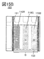
- 15A to 15D are top views of the pixel portion.
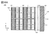
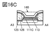
- 16A is a top view of the pixel portion and the connection portion
- FIG. 16B is a cross-sectional view of the pixel portion
- 16C is a cross-sectional view of the connection portion.
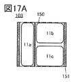
- 17A to 17E are top views of the pixel portion.
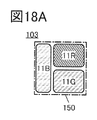
- 18A to 18E are top views of the pixel portion.
- 19A to 19C are cross-sectional views for explaining a method for manufacturing a display device.
- 20A to 20C are cross-sectional views for explaining a method for manufacturing a display device.
- 21A and 21B are cross-sectional views for explaining a method for manufacturing a display device.
- 22A and 22B are cross-sectional views for explaining a method for manufacturing a display device.
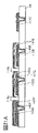
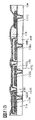
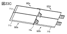
- 23A is a top view of the display device, and FIGS. 23B and 23C are perspective views of the display device.
- 24A and 24B are perspective views of the display device.
- FIGS. 25A to 25D are circuit diagrams.
- 26A to 26D are cross-sectional views of transistors.
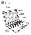
- 27A to 27D are diagrams of electronic devices.
- 28A and 28B are diagrams of electronic devices.
- 29A and 29B are diagrams of electronic equipment.
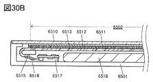
- 30A and 30B are diagrams of electronic devices.
- the terms “source” and “drain” of a transistor are interchanged depending on the polarity of the transistor and the level of the potential applied to each terminal.
- a terminal to which a low potential is applied is called a source
- a terminal to which a high potential is applied is called a drain
- a terminal to which a high potential is applied is called a source.
- the terms source and drain may be interchanged depending on the potential relationship, but in this specification and the like, when describing the connection relationship between transistors, the terms source and drain are fixed for convenience.
- a source of a transistor means a source region which is part of a semiconductor layer functioning as an active layer, or a source electrode connected to the source region.
- the drain of a transistor means a drain region that is part of the semiconductor layer or a drain electrode that is connected to the drain region.
- a gate of a transistor means a gate electrode.
- a state in which transistors are connected in series means, for example, a state in which only one of the source and drain of a first transistor is connected to only one of the source and drain of a second transistor.
- a state in which transistors are connected in parallel means that one of the source and drain of the first transistor is connected to one of the source and drain of the second transistor, and the other of the source and drain of the first transistor is connected to It means the state of being connected to the other of the source and the drain of the second transistor.
- connection may be referred to as electrical connection, and includes a state in which current, voltage, or potential can be supplied, or a state in which current, voltage, or potential can be transmitted. Therefore, it also includes a state in which they are connected to each other through elements such as wiring, resistors, diodes, and transistors.
- the electrical connection includes a state of direct connection without an element such as a wiring, resistor, diode, or transistor.
- a conductive layer may have multiple functions such as a wiring or an electrode.
- a light-emitting device is sometimes referred to as a light-emitting element.
- a light-emitting device has a structure in which an organic compound layer is sandwiched between a pair of electrodes. One of the pair of electrodes is an anode, the other of the pair of electrodes is a cathode, and at least one of the organic compound layers is a light-emitting layer.
- a light-emitting device having an organic compound layer formed using a metal mask may be referred to as a light-emitting device having a metal mask structure.
- the metal mask is sometimes referred to as a fine metal mask (FMM, high-definition metal mask) as the opening becomes finer.
- FMM fine metal mask
- a light-emitting device having an organic compound layer formed without using a metal mask or a fine metal mask may be referred to as a light-emitting device having a metal maskless (MML) structure.
- MML metal maskless
- a light-emitting device that emits red, green, blue, and the like may be referred to as a red-light-emitting device, a green-light-emitting device, and a blue-light-emitting device, respectively.
- a structure in which light-emitting layers are separately formed may be referred to as an SBS (side-by-side) structure.
- SBS side-by-side
- a full-color display device can be provided by fabricating a red light emitting device, a green light emitting device, and a blue light emitting device using the SBS structure.
- a light-emitting device that emits white light is sometimes referred to as a white light-emitting device.
- a white light-emitting device can provide a full-color display device by combining it with a colored layer (for example, a color filter or a color conversion layer).
- light-emitting devices can be broadly classified into a single structure and a tandem structure.
- a single structure is a structure having one light-emitting unit between a pair of electrodes.
- the light-emitting unit refers to a laminate including one or more light-emitting layers.
- two or more light-emitting layers should be included in the light-emitting unit, and light emitted from the two or more light-emitting layers should be recognized as white light.
- Two or more light-emitting layers may be in contact with each other in a light-emitting unit.
- a white light-emitting device can be obtained by satisfying a complementary color relationship.
- Three or more light-emitting layers may be in contact with each other in a light-emitting unit.
- a tandem structure is a structure having two or more light-emitting units between a pair of electrodes. Two or more light-emitting units each refer to a stack including one or more light-emitting layers. In the tandem structure, it is preferable to provide an intermediate layer such as a charge generation layer between the plurality of light emitting units. Note that the charge-generating layer has a function of injecting holes into a light-emitting unit formed in contact with the charge-generating layer when a voltage is applied between the cathode and the anode.
- the tandem structure preferably has a first light-emitting unit, a charge-generating layer, and a second light-emitting unit between a pair of electrodes, and holes are injected into the first light-emitting unit by the charge-generating layer. , electrons are injected into the second light-emitting unit.
- a structure in which white light emission is obtained by combining light from the light-emitting layers of two or more light-emitting units may be employed. Note that the combination of light-emitting layers for obtaining white light emission should satisfy the complementary color relationship, as in the case of the single structure.
- the light emitting device having the SBS structure consumes more power than the white light emitting device (single structure and tandem structure). can be lowered. If it is desired to keep power consumption low, it is preferable to use a light-emitting device with an SBS structure.
- white light-emitting devices are easier to manufacture than SBS structure light-emitting devices, so that the manufacturing cost can be reduced or the manufacturing yield can be increased. preferred.
- the display panel substrate is attached with a connector such as FPC (Flexible Printed Circuit) or TCP (Tape Carrier Package), or an IC is mounted on the substrate by the COG (Chip On Glass) method, etc.
- a module may be referred to as a display module.
- a display module is one aspect of a display device.
- a display device which is one embodiment of the present invention preferably includes an auxiliary wiring in a pixel portion.
- auxiliary wiring refers to a layer having an auxiliary function of the main electrode.
- an example of the "auxiliary function” is a function of suppressing a voltage drop that may occur in the main electrode.
- An example of the “main electrode” in this specification and the like is one of a pair of electrodes of a light-emitting device provided in a pixel portion. Since one of the pair of electrodes of the light-emitting device functions as one of the cathode and the anode of the light-emitting device, the conductive material used for one of the pair of electrodes of the light-emitting device is suitable for the cathode or the anode. has a work function Therefore, the conductive material used for either one of the pair of electrodes of the light emitting device may have high resistivity.
- the upper electrode is continuous without being separated between the plurality of light emitting devices.
- the series of electrodes is referred to as a “common electrode” in this specification and the like. difference between the voltage applied to A specific example of "voltage drop" in the above description of the auxiliary wiring is the voltage difference, and a specific example of "main electrode” is the common electrode.
- the auxiliary wiring is electrically connected to the common electrode.
- the voltage drop is suppressed more than when the auxiliary wiring is not electrically connected to the common electrode. It can be said that it is a function that suppresses the voltage drop that can occur.
- the auxiliary wiring is sometimes referred to as an auxiliary electrode according to its shape, but in this specification and the like, it may have any shape as long as it has the function of suppressing voltage drop that may occur in the common electrode. Note that in this specification and the like, one embodiment of the present invention is described using an auxiliary wiring.
- Metals such as aluminum, copper, silver, gold, platinum, chromium, and molybdenum can be used as the conductive material used for the auxiliary wiring.
- An alloy of the above metals can also be used as the conductive material.
- the metals and metal alloys mentioned above are preferred because of their low resistivity.
- metals and alloys of metals can have a lower conductivity compared to the conductive material used for the common electrode.
- the auxiliary wiring can have a single-layer structure or a laminated structure. Note that in the case of a laminated structure, the above-described conductive material may be used for at least one layer.
- the conductive material is a metal, a metal alloy, or a non-light-transmitting conductive material
- the performance of the display device does not deteriorate even when it is applied to the auxiliary wiring.
- the auxiliary wiring has a high degree of freedom in layout or shape, so it is possible to arrange it in a layout or shape that does not degrade the performance of the display device, for example.
- the method of manufacturing the auxiliary wiring using the conductive material is not limited at all.
- a conductive material having translucency may be used as the conductive material used for the auxiliary wiring.
- Examples of light-transmitting conductive materials include an oxide containing indium and tin (also referred to as indium tin oxide, In—Sn oxide, or ITO), and an oxide containing indium, silicon, and tin ( In—Si—Sn oxide, also called ITSO), an oxide containing indium and zinc (also called indium zinc oxide, In—Zn oxide), or an oxide containing indium, tungsten, and zinc (In ⁇ W—Zn oxide) or the like can be used.
- the auxiliary wiring can have a single-layer structure or a laminated structure.
- the above-described conductive material may be used for at least one layer. Since the conductive material is a translucent conductive material, the performance of the display device does not deteriorate even when it is applied to the auxiliary wiring. As described above, unlike the common electrode, the auxiliary wiring has a high degree of freedom in layout or shape. can be Note that the method of manufacturing the auxiliary wiring using the conductive material is not limited at all.
- An organic material such as a conductive polymer may be used for the auxiliary wiring, or an inorganic material such as carbon black may be used. Conductive polymers and carbon black can exhibit electrical conductivity. Using an organic material such as a conductive polymer can increase the height of the auxiliary wiring in a cross-sectional view. Using such a material, the auxiliary wiring can have a single-layer structure or a laminated structure. Note that in the case of a laminated structure, the above materials may be used for at least one layer. Note that the method of manufacturing the auxiliary wiring using the above material is not limited at all.
- the relation that the resistivity of the conductive material used for the auxiliary wiring is lower than the resistivity of the conductive material used for the common electrode is satisfied.
- the voltage drop can be sufficiently suppressed by increasing the thickness of the auxiliary wiring in a cross-sectional view, that is, by increasing the height.
- the voltage drop can be sufficiently suppressed by increasing the area of the auxiliary wiring in top view (this is referred to as plan view). In these cases, it is not necessary to satisfy the above relationship of resistivity.
- a display device which is one embodiment of the present invention preferably has a top emission structure.
- the electrode positioned on the light emitting side must be translucent. It means that light with a wavelength of 750 nm or more passes through, and it is desirable to have a transmittance of 40% or more. Further, it is preferable to use the electrode as a common electrode because the manufacturing method is simplified and the yield of the display device is improved.
- configuration A in which the common electrode is formed using a conductive material having a light-transmitting property, or a conductive material having no light-transmitting property is thinned. Therefore, a configuration B or the like is conceivable in which this is used as a common electrode.
- a translucent conductive material may have a high resistivity, and there is concern about a voltage drop.
- the configuration B when the thickness is reduced, the resistance of the common electrode increases and there is concern about voltage drop.
- the auxiliary wiring which is one embodiment of the present invention has a remarkable effect.
- the display device which is one embodiment of the present invention has a bottom-emission structure, it is needless to say that the effect of suppressing the voltage drop can be obtained by the structure including the auxiliary wiring electrically connected to the common electrode.
- a display device which is one embodiment of the present invention can have an imaging function by including a light-receiving device (also referred to as a light-receiving element) in a pixel portion.
- a light-receiving device also referred to as a light-receiving element
- a structure in which a light-receiving device is provided in a pixel portion is preferable because the number of parts can be reduced and the cost or size of the display device can be reduced as compared with a structure in which the light-receiving device is provided outside the display device. .
- the distance between the light receiving device and the light emitting device becomes shorter than when the light receiving device is provided outside.
- Part of the light may be received.
- Part of the light refers to light reflected or scattered at the interfaces of layers through which the light emitted from the light-emitting device passes, and is referred to as "stray light" in this specification and the like.
- the auxiliary wiring can prevent the light-receiving device from receiving stray light. In this specification and the like, this is sometimes referred to as "stray light suppression".
- Examples of a configuration in which the auxiliary wiring enhances the effect of suppressing stray light include configuration C in which the auxiliary wiring is positioned between the light receiving device and the light emitting device, and configuration D in which the auxiliary wiring is positioned so as to surround the light receiving device.
- a material capable of reflecting or absorbing stray light while having conductivity for the auxiliary wiring In order to reflect stray light, it is preferable to use a metal material for the auxiliary wiring. In order to absorb stray light, it is preferable to use a black material such as carbon black for the auxiliary wiring.
- the auxiliary wiring described above is called a "light shield" and an insulating material is used.
- the light blocking member may be positioned between the light receiving device and the light emitting device as in the configuration C, or may be positioned so as to surround the light receiving device as in the configuration D.
- the light shielding body is preferably high in cross-sectional view. Furthermore, it is preferable to use a material that reflects or absorbs stray light for the light shield.
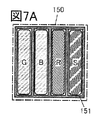
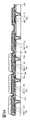
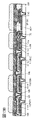
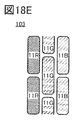
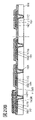
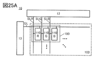
- FIGS. 1A to 1E are top views of a pixel portion 103 included in a display device. 1A to 1E show an X direction and a Y direction that intersects with the X direction, and the configuration and the like of the pixel portion 103 will be described using these directions.
- the pixel portion 103 is located in the display region and has a plurality of pixels 150 .
- a display device may have a protection circuit and/or a driver circuit in addition to the pixel portion 103 .
- Pixel 150 has at least sub-pixel 110R, sub-pixel 110G, and sub-pixel 110B.
- Sub-pixel 110R, sub-pixel 110G, and sub-pixel 110B correspond to light-emitting regions of respective light-emitting devices.
- sub-pixel 110B corresponds to the blue (sometimes referred to as B) light emitting region of the light emitting device.
- the display device of one embodiment of the present invention is not limited to the above emission colors, and may have a white light-emitting region in addition to the red, green, and blue light-emitting regions, for example.
- the sub-pixel 110R, the sub-pixel 110G, and the sub-pixel 110B are preferably arranged in a matrix (referred to as matrix arrangement).
- a matrix arrangement is a regular arrangement, and a plurality of sub-pixels 110R, 110G, and 110B are arranged in the entire pixel portion 103 according to the regular arrangement shown in the pixel 150.
- FIG. 1 A matrix arrangement is a regular arrangement, and a plurality of sub-pixels 110R, 110G, and 110B are arranged in the entire pixel portion 103 according to the regular arrangement shown in the pixel 150.
- the structure including at least the sub-pixel 110R, the sub-pixel 110G, and the sub-pixel 110B enables the display device which is one embodiment of the present invention to perform full-color display. Furthermore, in this embodiment, the display device has a light receiving portion 110S. Therefore, in this specification and the like, a group of the sub-pixels 110R, 110G, and 110B plus the light receiving section 110S is referred to as a pixel 150.
- a pixel 150 is used as "the minimum unit that enables full-color display”. Part may be included.
- the light receiving section 110S does not need to be arranged in all the pixels 150.
- the pixel 150 may not include the light-receiving portion 110 ⁇ /b>S, and the light-receiving portion 110 ⁇ /b>S is arranged at a rate of one for the plurality of pixels 150 , which is one embodiment of the present invention.
- the device may have imaging capabilities.
- the sub-pixel 110 has a light-emitting device that emits light of one color and a switching element that controls the light-emitting device.
- a display device can perform full color display by emitting light from a light emitting device controlled by a switching element.
- the sub-pixel 110R, sub-pixel 110G, and sub-pixel 110B may each have a colored layer, and examples of the colored layer include a color filter or a color conversion layer. In the top views shown in FIGS. 1A to 1E and the like, it may be considered that the colored layers are superimposed on the regions marked with RGB.
- the light receiving section 110S has a light receiving device. Further, the light receiving section 110S has a switching element that controls the light receiving device. A light receiving device controlled by a switching element has a function of receiving light from a light source and can convert the received light into an electrical signal. Therefore, the light receiving device is sometimes referred to as a photoelectric conversion device. Visible light or infrared light can be used for the light source of the light receiving device. In the case of visible light, the wavelength of light is not particularly limited, and examples thereof include light with wavelengths of blue, purple, blue-violet, green, yellow-green, yellow, orange, or red. The light receiving device is preferably capable of receiving one or more lights selected from the lights described above as visible light.
- the light emitted from each sub-pixel is used as a light source so that the light-receiving device can receive the light emitted from each sub-pixel.
- the light-receiving device can receive the light emitted from each sub-pixel.
- there is no need to provide a new light source which is preferable.
- One type of light emitted from each sub-pixel is green (with a typical wavelength of 480 nm or more and 560 nm or less). Green is preferable because it corresponds to a wavelength with high detection sensitivity of the light receiving device.
- Pixel 150 in FIG. 1A includes subpixel 110R, subpixel 110B adjacent to subpixel 110R in the X direction, subpixel 110G adjacent to subpixel 110R in the Y direction, and light receiving pixel adjacent to subpixel 110B in the Y direction. It has a part 110S.
- the auxiliary wiring 151 shown in FIG. 1A is provided in a region that does not overlap with the sub-pixel 110R, the sub-pixel 110G, the sub-pixel 110B, and the light receiving section 110S, and has a lattice shape in plan view.
- a grid is a pattern that combines a plurality of parallel vertical lines and a plurality of parallel horizontal lines.
- the auxiliary wiring 151 in FIG. 1A has regions extending along the X direction as horizontal lines, the regions being parallel to each other, and regions extending along the Y direction as vertical lines. are in parallel.
- the auxiliary wiring 151 shown in FIG. 1A is located between the sub-pixel 110R and the sub-pixel 110G as a region extending along the X direction, and the regions are arranged in parallel with a gap between the sub-pixels.
- the auxiliary wiring 151 shown in FIG. 1A is located between the sub-pixel 110R and the sub-pixel 110B as a region extending along the Y direction, and the regions are arranged in parallel with a gap between the sub-pixels.
- auxiliary wiring 151 shown in FIG. 1A By electrically connecting a common electrode (not shown in FIG. 1A) to the auxiliary wiring 151 shown in FIG. 1A, voltage drop caused by the common electrode can be suppressed. Further, since the auxiliary wiring 151 shown in FIG. 1A is arranged to surround the light receiving section 110S, it has a stray light suppression effect. In addition, when only the stray light suppressing effect is exhibited, the auxiliary wiring may be replaced with a light shield, and the arrangement of the light shield can be understood by referring to FIG. 1A.
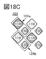
- FIG. 1B shows the same arrangement of pixels 150 as in FIG. 1A.
- the auxiliary wiring 151 shown in FIG. 1B is provided so as to sequentially surround the sub-pixels 110R, the light-receiving section 110S, and the like, which are arranged obliquely in the pixel section 103.
- the auxiliary wiring 151 shown in FIG. 1B has a region extending along the X direction and a region extending along the Y direction, and these regions can be read in the same manner as FIG. 1A based on FIG. 1B.
- the auxiliary wiring in FIG. 1B has less area than the auxiliary wiring in FIG. 1A.
- auxiliary wiring 151 shown in FIG. 1B By electrically connecting a common electrode (not shown in FIG. 1B) to the auxiliary wiring 151 shown in FIG. 1B, voltage drop caused by the common electrode can be suppressed. Further, since the auxiliary wiring 151 shown in FIG. 1B is arranged so as to surround the light receiving section 110S, it has a stray light suppression effect. In addition, when only the stray light suppressing effect is exhibited, the auxiliary wiring may be replaced with a light shield, and the arrangement of the light shield can be understood by referring to FIG. 1B.
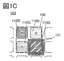
- FIG. 1C shows the same arrangement of pixels 150 as in FIG. 1A.
- the auxiliary wiring 151 shown in FIG. 1C is provided so as to surround at least the light receiving section 110S.
- the auxiliary wiring 151 shown in FIG. 1C has a region extending along the X direction and a region extending along the Y direction, and these regions can be read in the same manner as FIG. 1A based on FIG. 1C.
- the auxiliary wiring in FIG. 1C has less area than the auxiliary wiring in FIG. 1A.
- auxiliary wiring 151 shown in FIG. 1C By electrically connecting a common electrode (not shown in FIG. 1C) to the auxiliary wiring 151 shown in FIG. 1C, voltage drop caused by the common electrode can be suppressed. Furthermore, since the auxiliary wiring 151 shown in FIG. 1C has an arrangement provided so as to surround the light receiving section 110S, it has a stray light suppression effect. In addition, when only the stray light suppressing effect is exhibited, the auxiliary wiring may be replaced with a light shield, and the arrangement of the light shield can be understood by referring to FIG. 1C.
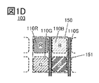
- FIG. 1D shows the same arrangement of pixels 150 as in FIG. 1A.
- the auxiliary wiring 151 shown in FIG. 1D is provided at least between the light receiving section 110S and the sub-pixel 110G.
- the auxiliary wiring 151 shown in FIG. 1D has a region extending along the Y direction, and the region can be read from the drawing in the same manner as in FIG. 1A.
- the auxiliary wiring in FIG. 1D has less area than the auxiliary wiring in FIG. 1A.
- auxiliary wiring 151 shown in FIG. 1D By electrically connecting a common electrode (not shown in FIG. 1D) to the auxiliary wiring 151 shown in FIG. 1D, voltage drop caused by the common electrode can be suppressed. Furthermore, since the auxiliary wiring 151 shown in FIG. 1D is arranged between the light receiving section 110S and the sub-pixel 110G, it has a stray light suppression effect. In addition, when only the stray light suppressing effect is exhibited, the auxiliary wiring may be replaced with a light shield, and the arrangement of the light shield can be understood by referring to FIG. 1D.
- FIG. 1E shows the same arrangement of pixels 150 as in FIG. 1A.
- the auxiliary wiring 151 shown in FIG. 1E is provided at least between the light receiving section 110S and the sub-pixel 110B.
- the auxiliary wiring 151 shown in FIG. 1E has a region extending along the X direction, and the region can be read from the drawing in the same manner as in FIG. 1A.
- the auxiliary wiring in FIG. 1E has less area than the auxiliary wiring in FIG. 1A.
- the auxiliary wiring 151 shown in FIG. 1E By electrically connecting the common electrode (not shown in FIG. 1E) to the auxiliary wiring 151 shown in FIG. 1E, the voltage drop caused by the common electrode can be suppressed. Furthermore, since the auxiliary wiring 151 shown in FIG. 1E is arranged between the light receiving section 110S and the sub-pixel 110B, it has a stray light suppression effect. In addition, when only the stray light suppressing effect is exhibited, the auxiliary wiring may be replaced with a light shield, and the arrangement of the light shield can be understood by referring to FIG. 1E.
- the arrangement of the auxiliary wiring 151 shown in FIGS. 1A to 1E is a position that does not reduce the aperture ratio and the like, and is commonly positioned at least in the vicinity of the light receiving section 110S. With the auxiliary wiring 151 shown in FIGS. 1A to 1E, both suppression of voltage drop and suppression of stray light can be achieved.
- auxiliary wiring 151 when a conductive material having translucency is used for the auxiliary wiring 151, even when the auxiliary wiring 151 overlaps with the sub-pixel and the light receiving section 110S, the aperture ratio and the like do not decrease.
- the arrangement of the auxiliary wiring 151 is not limited. However, if a conductive material having translucency is used for the auxiliary wiring 151, it becomes difficult to suppress stray light. It is preferable to combine with the auxiliary wiring 151 shown in 1E and use it as an auxiliary wiring of a laminated structure.
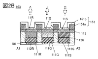
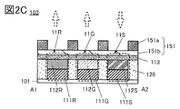
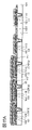
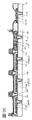
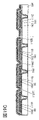
- FIGS. 2A to 2C show cross-sectional views corresponding to the dashed-dotted line A1-A2 shown in FIG. 1A.
- the cross-sectional structure of the auxiliary wiring 151 shown in FIGS. 2A to 2C can also be applied to the cross-sectional structure of the auxiliary wiring 151 and the like shown in FIGS. 1B to 1E.
- a light emitting device is located on the substrate 101 as shown in FIG. 2A.
- a light emitting device 11R corresponding to the sub-pixel 110R is positioned on the substrate 101.
- the light emitting device 11R can emit light toward the common electrode 113, that is, in the direction indicated by the arrow in FIG. 2A.
- a light emitting device 11G is positioned corresponding to the sub-pixel 110G.
- the lower electrode 111G of the light emitting device 11G is positioned on the substrate 101
- the organic compound layer 112G of the light emitting device 11G is positioned on the lower electrode 111G
- the common electrode 113 is positioned on the organic compound layer 112G.
- the light emitting device 11G can emit light toward the common electrode 113, that is, in the direction indicated by the arrow in FIG. 2A.
- the light emitting device 11B is positioned corresponding to the sub-pixel 110B. Specifically, the lower electrode 111B of the light emitting device 11B is positioned on the substrate 101, the organic compound layer 112B of the light emitting device 11B is positioned on the lower electrode 111B, and the common electrode 113 is positioned on the organic compound layer 112B.
- the light emitting device 11B can emit light to the common electrode 113 side.
- the light-emitting device 11 When describing matters common to the light-emitting device 11R, the light-emitting device 11G, and the light-emitting device 11B, the light-emitting device 11 may be referred to.
- the organic compound layer 112 When describing matters common to the organic compound layer 112R, the organic compound layer 112G, and the organic compound layer 112B, the organic compound layer 112 may be referred to.
- the light receiving device 11S is positioned corresponding to the light receiving section 110S. Specifically, the lower electrode 111S of the light receiving device 11S is positioned on the substrate 101, the active layer 112S of the light receiving device 11S is positioned on the lower electrode 111S, and the common electrode 113 is positioned on the active layer 112S.
- the light receiving device 11S can receive light as indicated by the arrow in FIG. 2A.
- a common electrode 113 is a common layer that each light emitting device has.
- the light receiving device 11S also has a common electrode 113.
- FIG. 2A the light receiving device 11S also has a common electrode 113.
- the lower electrode 111R, the lower electrode 111G, the lower electrode 111B, and the lower electrode 111S may be referred to as the lower electrode 111 when they are shown without distinction.
- the common electrode 113 When a top emission structure is applied to a display device which is one embodiment of the present invention, it is desirable that the common electrode 113 have high visible light transmittance. Specifically, the common electrode 113 may transmit 40% or more of visible light.
- the lower electrode 111 may transmit 40% or more of visible light.
- the display device which is one embodiment of the present invention is a bottom emission type. A voltage drop can be suppressed by providing an auxiliary wiring even in a bottom-emission display device.
- the display device according to one embodiment of the present invention is a dual-emission display device that emits light in both directions, that is, in the vertical direction of the substrate 101. type display device.
- a dual-emission display device can be described as a transparent display. Even in a dual-emission display device, a voltage drop can be suppressed by providing an auxiliary wiring.
- stray light from the light-emitting device is often caused by scattering or reflection in layers above the common electrode 113 . Therefore, in order to suppress stray light, it is preferable to provide an auxiliary wiring 151 on the common electrode 113 as shown in FIG. 2A. As described with reference to FIG. 1A and the like, the auxiliary wiring 151 is positioned on the common electrode 113 in a region that does not overlap with the light emitting device and the light receiving device in order to obtain the effect of not lowering the aperture ratio of the display device. do.
- an insulating layer 126 is positioned between each light emitting device and between light emitting and light receiving devices, as shown in FIG. 2A.
- the auxiliary wiring 151 may be positioned so as to overlap with the insulating layer 126 .
- the insulating layer 126 can separate the organic compound layers of each light-emitting device and suppress crosstalk between the light-emitting devices.
- the top surface of insulating layer 126 is shown to be generally coincident or coincident with the top surface of organic compound layer 112 .
- the common electrode 113 is preferably not cut off.
- the top surface of the insulating layer 126 may be positioned above the top surface of the organic compound layer 112 so that the common electrode 113 is not cut.
- the edges of the insulating layer 126 are preferably thinned gradually toward the center of the organic compound layer 112 .
- a shape that gradually becomes thinner is sometimes referred to as a tapered shape.
- the central portion of the insulating layer 126 is located above the edge portions of the insulating layer 126 and that the central portion has a region that rises above the edge portions.
- auxiliary wiring 151 has a region in contact with the upper surface of the common electrode 113 in FIG. 2A, voltage drop can be suppressed if the auxiliary wiring 151 can ensure electrical connection with the common electrode 113 .
- the light receiving device 11S shown in FIG. 2A can use light emitted from each light emitting device 11 as detection light.
- the detected light is visible light. It is preferable to use green light (with a typical wavelength of 480 nm or more and 560 nm or less) in visible light because the sensitivity of the light receiving device 11S is high. Therefore, the light receiving device 11S is preferably arranged adjacent to the light emitting device 11G. On the other hand, if the light from the light emitting device 11G becomes stray light and the light receiving device 11S receives the stray light, the detection sensitivity will decrease.
- the auxiliary wiring 151 is positioned at least in a region between the light receiving device 11S and the light emitting device 11G that emits detection light.
- the auxiliary wiring 151 can suppress a voltage drop caused by the common electrode 113 and can exhibit a stray light suppressing effect.
- FIG. 2B shows auxiliary wiring 151 having a laminated structure.
- a first auxiliary wiring 151a corresponding to the lower layer of the laminated structure can be provided in the same manner as the auxiliary wiring 151 in FIG. 2A.
- a conductive material having a light-transmitting property is preferably used for the second auxiliary wiring 151b located over the first auxiliary wiring 151a.
- the second auxiliary wiring 151b can be provided so as to have a region overlapping with the light emitting device. Since a light-transmitting conductive material may have high resistivity, the second auxiliary wiring 151b may be thicker than the first auxiliary wiring 151a.
- the auxiliary wiring 151 having a laminated structure suppresses the voltage drop caused by the common electrode 113 and has the effect of suppressing stray light.
- FIG. 2B the configuration other than the auxiliary wiring having a laminated structure is the same as that in FIG. 2A.
- FIG. 2C shows an auxiliary wiring 151 having a laminated structure, the order of which is different from that of the auxiliary wiring 151 shown in FIG. 2B.
- the first auxiliary wiring 151a is positioned on the second auxiliary wiring 151b.
- the materials and the like of the first auxiliary wiring 151a and the second auxiliary wiring 151b are the same as those in FIG. 2B.
- the auxiliary wiring 151 having a laminated structure can suppress the reception of stray light while suppressing the voltage drop of the common electrode 113 .
- FIG. 2C the configuration other than the auxiliary wiring having a laminated structure is the same as in FIG. 2A.
- the auxiliary wiring 151 having the cross-sectional structure as shown in FIGS. 2A to 2C is provided, the voltage drop caused by the common electrode 113 can be suppressed, and the display quality can be improved.
- the auxiliary wiring 151 has a region located on the common electrode 113, it has the effect of suppressing stray light and can increase the detection sensitivity of the light receiving device.
- the organic compound layer can be cut by the insulating layer 126, crosstalk or the like can be suppressed.
- the organic compound layer can be finely processed, a high-definition display device can be provided.
- a display device of one embodiment of the present invention is described using an SBS structure in which light-emitting devices that emit light of different colors are separately manufactured.
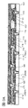
- Example 1 Specific Example 1 of the display device of one embodiment of the present invention will be described with reference to FIGS. 3A to 3C.
- the display device 100 has a pixel portion 103 and a connection portion 140 .
- the pixel portion 103 has a plurality of pixels 150 .
- the pixel 150 has a plurality of sub-pixels 110.
- the sub-pixel 110R has a red light-emitting device 11R
- the sub-pixel 110G has a green light-emitting device 11G
- the sub-pixel 110B has a blue light-emitting device 11B.
- the pixel 150 has a light receiving portion 110S
- the light receiving portion 110S has a light receiving device 11S.
- FIG. 3A the regions corresponding to the light emitting device 11R, the light emitting device 11G, the light emitting device 11B, and the light receiving device 11S are labeled R, G, B, and S.
- the arrangement of FIG. 3A is similar to the arrangement shown in FIG. 1A and the like, and is a regular arrangement.
- Elements such as OLEDs (Organic Light Emitting Diodes) or QLEDs (Quantum-dot Light Emitting Diodes) are preferably used as the light emitting devices 11R, 11G, and 11B.
- the light-emitting substances possessed by the light-emitting device include substances that emit fluorescence (fluorescent materials), substances that emit phosphorescence (phosphorescent materials), inorganic compounds (quantum dot materials, etc.), and substances that exhibit heat-activated delayed fluorescence (heat-activated delayed fluorescence (thermally activated delayed fluorescence: TADF) material) and the like.
- connection electrode 111C electrically connected to the common electrode 113.
- the common electrode 113 preferably extends to the connection portion 140 beyond the edge of the pixel portion 103 .
- the common electrode 113 extending to the connection portion 140 is indicated by a dotted line.
- a potential to be supplied to the common electrode 113 is applied to the connection electrode 111C. If a voltage drop occurs due to the common electrode 113, the potential value will vary. Since the display device of this embodiment mode includes the auxiliary wiring 151 at least in the pixel 150, it is preferable that the potential values do not vary.
- the auxiliary wiring 151 can be provided in the connection portion 140 in addition to the pixel portion 103 .
- connection electrode 111 ⁇ /b>C can be provided along the outer periphery of the pixel portion 103 .
- the connection electrode 111C may be provided along one side of the periphery of the pixel portion 103, or may be provided over two or more sides of the periphery of the pixel portion 103.
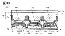
- FIG. 3B and 3C are cross-sectional views corresponding to the dashed-dotted line A1-A2 and the dashed-dotted line A3-A4 in FIG. 3A, respectively.
- FIG. 3B shows cross-sectional views of the light-emitting device 11R, the light-emitting device 11G, and the light-receiving device 11S
- FIG. 3C shows a cross-sectional view of the connection electrode 111C.
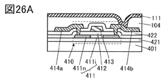
- the light-emitting device 11R has a lower electrode 111R, an organic compound layer 112R, a common layer 114, and a common electrode 113.
- FIG. The light emitting device 11G has a lower electrode 111G, an organic compound layer 112G, a common layer 114 and a common electrode 113.
- the light emitting device 11B has a lower electrode 111B, an organic compound layer 112B, a common layer 114, and a common electrode 113.
- FIG. A functional layer that can be used for the common layer 114 is, for example, an electron injection layer.
- the lower electrode is an electrode electrically connected to the transistor and is sometimes referred to as a pixel electrode.
- the bottom electrode also functions as one of the anode or cathode of the light emitting device and is sometimes referred to as the anode or the cathode.
- the organic compound layer 112R contains a light-emitting organic compound that emits light having an intensity in at least the red wavelength range.
- the organic compound layer 112G contains a light-emitting organic compound that emits light having an intensity in at least the green wavelength range.
- the organic compound layer 112B contains a light-emitting organic compound that emits light having an intensity in at least the blue wavelength range.
- a layer containing a light-emitting organic compound can be referred to as a light-emitting layer.
- the organic compound layer 112 and the common layer 114 can each independently have one or more layers selected from an electron injection layer, an electron transport layer, a light-emitting layer, a hole injection layer, and a hole transport layer.
- An electron injection layer, an electron transport layer, a light-emitting layer, a hole injection layer, and a hole transport layer may be referred to as functional layers. Having two or more layers includes combining two or more different functional layers and having two or more layers having the same functional layer but different materials in combination. Specific materials that can be used for the functional layer will be described later.
- the organic compound layer 112 has a layered structure of a hole-injection layer, a hole-transport layer, a light-emitting layer, and an electron-transport layer in this order from the lower electrode 111 side, and the common layer 114 is an electron-injection layer. shall be configured to have
- the functional layer does not necessarily need to contain an organic compound as long as it can exhibit each function.
- a film containing only an inorganic compound or an inorganic substance can be used for the electron injection layer or the like.
- the lower electrode 111R, the lower electrode 111G, and the lower electrode 111B are provided for each light emitting device. Also, the common electrode 113 and the common layer 114 are provided as a continuous layer common to each light emitting device. A reflective conductive film is used for each lower electrode, and a conductive film having a property of transmitting visible light is used for the common electrode 113, so that the display device can have a top-emission structure.
- the end of the lower electrode 111 preferably has a tapered shape.
- the term “tapered shape” refers to a shape in which at least a part of the side surface of the structure is inclined with respect to the substrate surface or the formation surface. For example, if a region in which an angle between the inclined side surface and the substrate surface (also referred to as a taper angle) is less than 90° can be confirmed, it can be said that the structure has a tapered shape. Note that even when the inclined side surface of the structure has a substantially planar shape with a fine curvature or a substantially planar shape with fine unevenness, it may be called a tapered shape.
- the end of the organic compound layer 112 is preferably positioned beyond the end of the lower electrode 111, and when the end of the lower electrode 111 has a tapered shape, the organic compound layer 112 has a shape along the tapered shape. Since the side surface of the lower electrode 111 is tapered, coverage with an organic compound layer or the like is enhanced. Furthermore, the tapered side surface of the lower electrode 111 facilitates removal of foreign substances (eg, dust, particles, or the like) during the manufacturing process by cleaning or the like, which is preferable.
- foreign substances eg, dust, particles, or the like
- the organic compound layer 112 is processed by photolithography. Therefore, the angle formed by the end of the organic compound layer 112 with the substrate surface or the formation surface is close to 90 degrees, and the end of the organic compound layer 112 may not have a tapered shape. Such an end of the organic compound layer 112 is preferably located in a region beyond the end of the lower electrode 111 .
- an insulating layer 126 between the organic compound layers whose ends do not have a tapered shape, specifically between two adjacent light emitting devices.
- the insulating layer 126 is provided so as to fill at least between two adjacent organic compound layers 112 . More preferably, the insulating layer 126 has a region overlapping with the edge of the organic compound layer 112 . Positioning the insulating layer 126 so as to partially overlap the organic compound layer 112 makes it possible to reduce the height difference between the upper portion of the insulating layer 126 and the height of the light emitting device after the insulating layer 126 is formed. The difference is preferably small because the insulating layer 126 may be easily peeled off.
- the upper portion of the insulating layer 126 preferably has a convex shape, preferably a smooth convex shape.
- the upper portion having a convex shape can also be described as a shape in which the central portion of the insulating layer 126 is raised more than the end portions.
- the common layer 114 and the common electrode 113 By providing the common layer 114 and the common electrode 113 so as to cover the insulating layer 126 having a shape in which the central portion is raised from the end portions, at least the common layer 114 and the common electrode 113 can be prevented from being cut.
- the insulating layer 125 is provided in contact with the side surface of the organic compound layer 112 before the insulating layer 126 is formed.
- the insulating layer 125 is positioned between the insulating layer 126 and the organic compound layer 112 and functions as a protective film to prevent the insulating layer 126 from contacting the organic compound layer 112 .
- the organic compound layer 112 may be dissolved by an organic solvent or the like used when forming or processing the insulating layer 126 . Therefore, by providing the insulating layer 125 between the organic compound layer 112 and the insulating layer 126 as shown in this embodiment mode, the organic compound layer 112 can be protected.
- the insulating layer 125 can be an insulating layer containing an inorganic material.
- an inorganic insulating film such as an oxide insulating film, a nitride insulating film, an oxynitride insulating film, or a nitride oxide insulating film can be used, for example.
- the insulating layer 125 may have a single-layer structure or a laminated structure.
- the oxide insulating film includes a silicon oxide film, an aluminum oxide film, a magnesium oxide film, an indium gallium zinc oxide film, a gallium oxide film, a germanium oxide film, an yttrium oxide film, a zirconium oxide film, a lanthanum oxide film, a neodymium oxide film, and an oxide film.
- a hafnium film, a tantalum oxide film, and the like are included.
- the nitride insulating film include a silicon nitride film and an aluminum nitride film.
- Examples of the oxynitride insulating film include a silicon oxynitride film, an aluminum oxynitride film, and the like.
- nitride oxide insulating film a silicon nitride oxide film, an aluminum nitride oxide film, or the like can be given.
- a metal oxide film such as an aluminum oxide film or a hafnium oxide film formed by the ALD method, or an inorganic insulating film such as a silicon oxide film to the insulating layer 125, there are few pinholes and the function of protecting the organic compound layer.
- An insulating layer 125 having excellent resistance can be formed.
- oxynitride refers to a material whose composition contains more oxygen than nitrogen
- nitride oxide refers to a material whose composition contains more nitrogen than oxygen. point to the material.
- silicon oxynitride refers to a material whose composition contains more oxygen than nitrogen
- silicon nitride oxide refers to a material whose composition contains more nitrogen than oxygen. indicates
- the insulating layer 125 may be formed by a sputtering method, a chemical vapor deposition (CVD) method, a pulsed laser deposition (PLD) method, an atomic layer deposition (ALD) method, or the like. can be done.
- the insulating layer 125 is preferably formed by an ALD method with good coverage.
- an insulating layer containing an organic material can be preferably used.
- acrylic resin, polyimide resin, epoxy resin, imide resin, polyamide resin, polyimideamide resin, silicone resin, siloxane resin, benzocyclobutene resin, phenolic resin, and precursors of these resins are applied. can do.
- an organic material such as polyvinyl alcohol (PVA), polyvinyl butyral, polyvinylpyrrolidone, polyethylene glycol, polyglycerin, pullulan, water-soluble cellulose, or alcohol-soluble polyamide resin may be used as the insulating layer 126 .
- a photosensitive resin can be used for the insulating layer 126 .
- a photoresist may be used as the photosensitive resin.
- a positive material or a negative material can be used for the photosensitive resin.
- a starting material of a photosensitive material is diluted with a diluent to 2 to 10 times, preferably 2 to 4 times, and used.
- the film thickness of the insulating layer 126 is 0.8 ⁇ m or more and 1.2 ⁇ m or less.
- the film thickness of the insulating layer 126 is 0.4 ⁇ m or more and 0.6 ⁇ m or less.
- the film thickness of the insulating layer 126 is 0.5 ⁇ m or more and 0.7 ⁇ m or less.
- Using a diluted starting material can reduce the film thickness and suppress the amount of outgassing from the insulating layer 126 .
- the starting material has a viscosity of 3 cP or more and 10 cP or less, preferably 5 cP or more and 7 cP or less, the film thickness can be reduced.
- the processed insulating layer 126 can be formed by exposure and development.
- the surface of the processed insulating layer 126 may have a rounded shape or an uneven shape. Note that etching may be performed in order to adjust the height of the surface of the processed insulating layer 126 .
- the insulating layer 126 can be processed by ashing using oxygen plasma to adjust the surface height.
- the insulating layer 126 preferably contains a material that absorbs visible light. If a material that absorbs visible light is used, the stray light suppressing effect can be exhibited in combination with the auxiliary electrode.
- the insulating layer 126 itself may be made of a material that absorbs visible light, or the insulating layer 126 may contain a pigment that absorbs visible light.
- a resin that transmits red, blue, or green light and can be used as a color filter that absorbs other light, or a resin that contains carbon black as a pigment and functions as a black matrix, or the like. can also be used.
- the upper portion of the insulating layer 126 preferably has a portion higher than the upper surface of the organic compound layer 112 .
- the insulating layer 126 is formed using a wet deposition method such as spin coating, dipping, spray coating, inkjet, dispensing, screen printing, offset printing, doctor knife method, slit coating, roll coating, curtain coating, or knife coating. can be formed. In particular, it is preferable to form an organic insulating film to be the insulating layer 126 by spin coating.
- heat treatment is preferably performed in the air at 85° C. to 120° C. for 45 minutes to 100 minutes.
- dehydration or degassing from the insulating layer 126 can be performed.
- a reflective film (eg, a metal film containing one or more selected from silver, palladium, copper, titanium, aluminum, and the like) may be provided between the insulating layer 125 and the insulating layer 126 .
- the reflective film can be formed after forming the insulating layer 125 .
- the light emitted from the light-emitting layer can be reflected by the reflective film. Thereby, the light extraction efficiency can be improved.
- an insulating layer 128 may be provided between the insulating layer 125 and the top surface of the organic compound layer 112 .
- the insulating layer 128 is a part of a protective layer (also referred to as a sacrificial layer) for protecting the organic compound layer 112 when the organic compound layer 112 is etched.
- a material that can be used for the insulating layer 125 is preferably used for the insulating layer 128 .
- both the insulating layer 128 and the insulating layer 125 preferably include an aluminum oxide film, a hafnium oxide film, or a silicon oxide film.
- the insulating layer 125, the insulating layer 126, and the insulating layer 128 are all insulating layers located between the light emitting devices, and in this specification and the like, they may be collectively referred to as an "insulating laminate". Since the common layer 114 and the common electrode 113 are provided on the insulating laminate, the end of the insulating laminate preferably has a tapered shape so that the common layer 114 and the common electrode 113 are not cut off. In order for the end of the insulating laminate to have a tapered shape, the end of the insulating layer 125 may have a tapered shape, the end of the insulating layer 126 may have a tapered shape, or the insulating layer 128 may have a tapered shape.
- the tapered shape may have a tapered shape, or the ends of the insulating layer 125, the insulating layer 126, and the insulating layer 128 may all have a tapered shape.
- the tapered shape is formed by a plurality of insulating layers, it is preferable that the tapered shape at the end of each insulating layer is formed continuously.
- the central portion of the insulating laminate has a rounded upper surface. That is, the central portion of the insulating laminate has a shape that rises more than the ends.
- the insulating layer 126 located at the uppermost layer of the insulating laminate is preferably formed using an organic material.
- the ends of the insulating laminate can have a variety of shapes.
- the insulating layer 125 located below the insulating laminate may protrude from the insulating layer 126 .
- part of the upper portion of the insulating layer 125 may be removed when the insulating layer 126 is processed.
- the upper portion of the insulating layer 125 protruding from the insulating layer 126 is removed, there is an effect that the common layer 114 and the common electrode 113 are not disconnected.
- Insulating layer 128 may protrude from insulating layer 126 . In this case, part of the upper portion of the insulating layer 128 may be removed when the insulating layer 126 is processed. When the upper part of the insulating layer 128 protruding from the insulating layer 126 is removed, there is an effect that the common layer 114 and the common electrode 113 are not disconnected.
- the edge of the insulating layer 125 located below the insulating layer 128 may coincide or substantially coincide with the edge of the insulating layer 128 .
- An auxiliary wiring 151 is provided on the common electrode 113 .
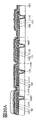
- the thickness of the auxiliary wiring 151 (the distance indicated by Ha in FIG. 3B) will be described.
- the thickness (Ha) of the auxiliary wiring 151 is preferably less than half the distance from the lower surface of the auxiliary wiring 151 to the substrate 170 (distance Hb in FIG. 3B). In this case, the effect of suppressing stray light and the effect of suppressing voltage drop can be sufficiently exhibited.
- the common electrode 113 and the auxiliary wiring 151 are attached to the substrate 170 with an adhesive layer 171 .
- an adhesive layer 171 various curable adhesives such as photocurable adhesives such as ultraviolet curable adhesives, reaction curable adhesives, thermosetting adhesives, and anaerobic adhesives can be used.
- an adhesive sheet or the like may be used for the adhesive layer 171 .
- connection portion 140 shown in FIG. 3C an opening is provided in the insulating layer 125 and the insulating layer 126 above the connection electrode 111C.
- the connection electrode 111C and the common electrode 113 are electrically connected through the opening.
- An opening for electrically connecting the connection electrode 111C and the common electrode 113 may be provided in any insulating layer.
- FIG. 3C shows the connection portion 140 in which the connection electrode 111C has a region in contact with the common electrode 113, but the common layer 114 is provided on the connection electrode 111C, and the common electrode 113 is provided on the common layer 114.
- a carrier injection layer such as an electron injection layer
- the material used for the common layer 114 has a sufficiently low resistivity. can be electrically connected.
- the common electrode 113 and the common layer 114 can be formed using the same mask (also referred to as an area mask or a rough metal mask to distinguish it from a fine metal mask), so manufacturing costs can be reduced.
- Example 2 Specific Example 2 of the display device of one embodiment of the present invention will be described with reference to FIG. 4A.
- FIG. 4A differs from FIG. 3B and the like in that the top shape of the insulating layer 126 has a flat region.
- the configuration of the end portion of the insulating layer 126 is the same as in FIG. 3B.
- the shape of the insulating layer 126 can be changed depending on the material used for the insulating layer 126 or the manufacturing conditions.
- a common layer 114 and a common electrode 113 are provided to cover the upper surface of the insulating layer 126 having a flat top shape.
- Auxiliary wiring 151 is provided on the insulating layer 126 via the common electrode 113 and the like.
- the top surface of the common electrode 113 which is the surface on which the auxiliary wiring 151 is formed, has a shape along the top surface of the insulating layer 126 .
- the auxiliary wiring 151 on the flat formation surface can have a shape in which the width is wider than the height, and voltage drop can be sufficiently suppressed.
- Other configurations are the same as those in FIG. 3B and the like.
- the auxiliary wiring 151 can suppress a voltage drop while exhibiting a stray light suppressing effect.
- Example 3 Specific Example 3 of the display device of one embodiment of the present invention will be described with reference to FIG. 4B.
- an auxiliary wiring 151 having a laminated structure is provided. Specifically, a second auxiliary wiring 151b is provided on the first auxiliary wiring 151a.
- the first auxiliary wiring 151a can be provided in the same manner as the auxiliary wiring 151 in FIG. 4A.
- the second auxiliary wiring 151b includes a light-transmitting conductive material and can be provided so as to have a region overlapping with the light-emitting device.
- the film thickness of the second auxiliary wiring 151b may be larger than the film thickness of the first auxiliary wiring 151a.
- Other configurations are the same as those in FIG. 4A and the like.
- the auxiliary wiring 151 having a laminated structure can suppress a voltage drop and achieve a stray light suppressing effect.
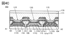
- Example 4 Specific Example 4 of the display device of one embodiment of the present invention will be described with reference to FIG. 4C.
- an auxiliary wiring 151 having a laminated structure is provided. Specifically, the order of stacking is different from that of the auxiliary wiring 151 in FIG. 4B, and the first auxiliary wiring 151a is provided on the second auxiliary wiring 151b.
- the second auxiliary wiring 151b includes a light-transmitting conductive material and can be provided so as to have a region overlapping with the light-emitting device.
- the first auxiliary wiring 151a can be provided in the same manner as the auxiliary wiring 151 in FIG. 4A.
- the film thickness of the second auxiliary wiring 151b may be larger than the film thickness of the first auxiliary wiring 151a.
- Other configurations are the same as those in FIG. 4A and the like.
- the auxiliary wiring 151 having a laminated structure can suppress a voltage drop and achieve a stray light suppressing effect.
- Example 5 Specific Example 5 of the display device of one embodiment of the present invention will be described with reference to FIG. 5A.
- a substrate 170 is provided with a light shielding layer 152 .
- the auxiliary wiring 151 preferably has a region in contact with the light shielding layer 152 .
- Other configurations are the same as those in FIG. 3B and the like.
- the auxiliary wiring 151 can suppress a voltage drop while exhibiting a stray light suppressing effect.
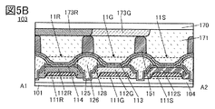
- Example 6 Specific Example 6 of the display device of one embodiment of the present invention will be described with reference to FIG. 5B.
- the substrate 170 is provided with a colored layer 173R that transmits red light and a colored layer 173G that transmits green light.
- a colored layer 173B that transmits blue light is provided at a position overlapping with the light emitting device 11B.
- the edge of the colored layer 173R may have a region that overlaps the edge of the colored layer 173G.
- the edge of the colored layer 173G may have a region that overlaps the edge of the colored layer 173B. These overlapping regions can function as light shielding regions.
- the colored layer 173 When describing matters common to the colored layer 173R, the colored layer 173G, and the colored layer 173B, the colored layer 173 may be referred to.
- the auxiliary wiring 151 preferably has a region in contact with the colored layer 173 .
- Other configurations are the same as those in FIG. 3B and the like.
- the auxiliary wiring 151 can suppress a voltage drop while exhibiting a stray light suppressing effect.
- Example 7 Specific Example 7 of the display device of one embodiment of the present invention will be described with reference to FIG. 5C.
- a substrate 170 is provided with a colored layer 173R and a colored layer 173G, and a light shielding layer 152 is provided in an overlapping region.
- the auxiliary wiring 151 preferably has a region in contact with the colored layer 173 .
- Other configurations are the same as those in FIG. 3B and the like.
- the auxiliary wiring 151 can suppress a voltage drop while exhibiting a stray light suppressing effect.
- the display device of one embodiment of the present invention is described using an SBS structure in which light-emitting devices that emit light of different colors are separately manufactured.
- an example of a display device capable of performing full-color display by combining a plurality of light-emitting devices that emit white light and colored layers will be described.
- a color filter or a color conversion layer can be used for the colored layer.
- a light-emitting device that emits white light preferably has a tandem structure, but may have a single structure.
- the display shown in FIG. 6A mainly differs from the display shown in FIG. 5B in that it has a light emitting device that emits white light.
- the display device shown in FIG. 6A has a plurality of light emitting devices 11W.
- the light-emitting device 11W has an organic compound layer 112W that emits white light.
- the substrate 170 is provided with a colored layer 173R and a colored layer 173G. Although not shown in FIG. 6A, it has a colored layer 173B.
- the white light emitted from the light-emitting device 11W is colored by absorbing light in a predetermined wavelength range by the colored layer 173R, the colored layer 173G, or the colored layer 173B, and is emitted to the outside through the substrate 170, resulting in full-color light. display is possible.
- FIG. 6B shows an example in which a light shielding layer 152 is applied to the configuration illustrated in FIG. 6A.
- the light shielding layer 152 is provided on the substrate 170 side, similarly to the colored layer 173 .
- the colored layer 173 preferably has a region overlapping with the light shielding layer 152 .
- FIG. 6B shows an example in which the colored layer 173 has a portion located between the light shielding layers 152 .
- the display devices described in the specific example and modified example have a common structure in which at least the organic compound layer is cut. With this structure, crosstalk due to leakage current is suppressed, and an image with extremely high display quality can be displayed. Furthermore, it is possible to achieve both a high aperture ratio and high definition. Therefore, it can be used for an ultra-compact display (microdisplay) for a head-mounted display. Note that the display device of one embodiment of the present invention is not limited to this, and can be applied to an ultra-small display of less than 1 inch to an ultra-large display of more than 100 inches.
- a light-transmitting conductive film is used for the electrode on the side from which light is extracted in the light-emitting device, and a conductive film that reflects visible light is used for the electrode on the side from which light is not extracted.
- a conductive film that reflects visible light and a conductive film that transmits visible light may be used for the electrode on the side from which light is not extracted.
- the electrode is preferably placed between the conductive film that reflects visible light and the organic compound layer. In other words, the light emitted from the light-emitting device only needs to be reflected by the conductive film that reflects visible light and extracted from the display device.
- Metals, alloys, electrically conductive compounds, mixtures thereof, and the like can be appropriately used as materials for forming the electrodes of the light-emitting device.
- aluminum-containing alloys also referred to as aluminum alloys
- silver-magnesium alloys also referred to as MgAg
- silver-palladium-copper alloys Ag-Pd-Cu, also referred to as APC).
- metals such as aluminum, titanium, chromium, manganese, iron, cobalt, nickel, copper, gallium, zinc, indium, tin, molybdenum, tantalum, tungsten, palladium, gold, platinum, silver, yttrium, neodymium, etc. Alloys containing suitable combinations may also be used.
- elements belonging to Group 1 or Group 2 of the periodic table of elements not exemplified above e.g., lithium, cesium, calcium, strontium
- europium such as ytterbium, alloys containing appropriate combinations of these, graphene, etc.
- those that can emit holes can be used as the anode, and those that can emit electrons can be used as the cathode.
- the light-emitting device employs a micro-optical resonator (microcavity) structure. Therefore, one of the pair of electrodes of the light-emitting device preferably has an electrode (semi-transmissive/semi-reflective electrode) that is transparent and reflective to visible light, and the other is an electrode that is reflective to visible light ( reflective electrode). Since the light emitting device has a microcavity structure, light emission can be resonated between the pair of electrodes, and the light emitted from the light emitting device can be narrowed and further enhanced.
- microcavity micro-optical resonator
- micro-optical resonator microcavity
- the distance between a pair of electrodes is different in red, green and blue light emitting devices.
- a semi-transmissive/semi-reflective electrode is a thin film of a reflective electrode that partially transmits visible light, or a laminated structure of a reflective electrode and an electrode that transmits visible light (also called a transparent electrode). can be used.
- the light transmittance of the transparent electrode is set to 40% or more.
- the light-emitting device preferably uses an electrode having a transmittance of 40% or more for visible light (light with a wavelength of 400 nm or more and less than 750 nm).
- the visible light reflectance of the reflective electrode is 40% or more and 100% or less, preferably 70% or more and 100% or less.
- the organic compound layer of the light-emitting device has at least a light-emitting layer.
- a light-emitting layer is a layer containing a light-emitting material (also referred to as a light-emitting substance).
- the emissive layer can have one or more emissive materials.
- As the light-emitting substance a substance exhibiting emission colors such as blue, purple, blue-violet, green, yellow-green, yellow, orange, and red is used as appropriate.
- a substance that emits near-infrared light can be used as the light-emitting substance.
- Examples of light-emitting substances include fluorescent materials, phosphorescent materials, TADF materials, quantum dot materials, and the like.
- fluorescent materials include pyrene derivatives, anthracene derivatives, triphenylene derivatives, fluorene derivatives, carbazole derivatives, dibenzothiophene derivatives, dibenzofuran derivatives, dibenzoquinoxaline derivatives, quinoxaline derivatives, pyridine derivatives, pyrimidine derivatives, phenanthrene derivatives, naphthalene derivatives, and the like. be done.
- Examples of phosphorescent materials include organometallic complexes (especially iridium complexes) having a 4H-triazole skeleton, 1H-triazole skeleton, imidazole skeleton, pyrimidine skeleton, pyrazine skeleton, or pyridine skeleton, and phenylpyridine derivatives having an electron-withdrawing group.
- organometallic complexes especially iridium complexes
- platinum complexes, rare earth metal complexes, etc. which are used as ligands, can be mentioned.
- the light-emitting layer may contain one or more organic compounds (host material, assist material, etc.) in addition to the light-emitting substance (guest material).
- One or both of a hole-transporting material and an electron-transporting material can be used as the one or more organic compounds.
- Bipolar materials or TADF materials may also be used as one or more organic compounds.
- the light-emitting layer preferably includes, for example, a phosphorescent material and a combination of a hole-transporting material and an electron-transporting material that easily form an exciplex.
- ExTET Exciplex-Triplet Energy Transfer
- a combination that forms an exciplex that emits light that overlaps with the wavelength of the absorption band on the lowest energy side of the light-emitting substance energy transfer becomes smooth and light emission can be efficiently obtained. With this configuration, high efficiency, low-voltage driving, and long life of the light-emitting device can be realized at the same time.
- the organic compound layer 112 includes, as layers other than the light-emitting layer, a substance with a high hole-injection property, a substance with a high hole-transport property, a hole-blocking material, a substance with a high electron-transport property, a substance with a high electron-injection property, A layer containing an electron-blocking material, a bipolar substance (a substance with high electron-transporting and hole-transporting properties), or the like may be further included.
- Both low-molecular-weight compounds and high-molecular-weight compounds can be used in the light-emitting device, and inorganic compounds may be included.
- Each of the layers constituting the light-emitting device can be formed by a vapor deposition method (including a vacuum vapor deposition method), a transfer method, a printing method, an inkjet method, a coating method, or the like.
- each of the organic compound layers 112 may have one or more of a hole injection layer, a hole transport layer, a hole blocking layer, an electron blocking layer, an electron transport layer, and an electron injection layer.
- One or more of a hole injection layer, a hole transport layer, a hole block layer, an electron block layer, an electron transport layer, and an electron injection layer may be applied as the common layer 114 .
- a carrier injection layer (hole injection layer or electron injection layer) may be formed as the common layer 114 . Note that the light emitting device need not have the common layer 114 .
- the hole-injecting layer is a layer that injects holes from the anode to the hole-transporting layer, and contains a material with high hole-injecting properties.
- highly hole-injecting materials include aromatic amine compounds and composite materials containing a hole-transporting material and an acceptor material (electron-accepting material).
- the hole-transporting layer is a layer that transports holes injected from the anode to the light-emitting layer by means of the hole-injecting layer.
- a hole-transporting layer is a layer containing a hole-transporting material.
- a substance having a hole mobility of 10 ⁇ 6 cm 2 /Vs or more is preferable as the hole-transporting material. Note that substances other than these can be used as long as they have a higher hole-transport property than electron-transport property.
- hole-transporting materials include materials with high hole-transporting properties such as ⁇ -electron-rich heteroaromatic compounds (e.g., carbazole derivatives, thiophene derivatives, furan derivatives, etc.) and aromatic amines (compounds having an aromatic amine skeleton). is preferred.
- ⁇ -electron-rich heteroaromatic compounds e.g., carbazole derivatives, thiophene derivatives, furan derivatives, etc.
- aromatic amines compounds having an aromatic amine skeleton
- the electron-transporting layer is a layer that transports electrons injected from the cathode to the light-emitting layer by the electron-injecting layer.
- the electron-transporting layer is a layer containing an electron-transporting material.
- an electron-transporting material a substance having an electron mobility of 1 ⁇ 10 ⁇ 6 cm 2 /Vs or more is preferable. Note that substances other than these substances can be used as long as they have a higher electron-transport property than hole-transport property.
- electron-transporting materials include metal complexes having a quinoline skeleton, metal complexes having a benzoquinoline skeleton, metal complexes having an oxazole skeleton, metal complexes having a thiazole skeleton, oxadiazole derivatives, triazole derivatives, imidazole derivatives, ⁇ electron deficient including oxazole derivatives, thiazole derivatives, phenanthroline derivatives, quinoline derivatives with quinoline ligands, benzoquinoline derivatives, quinoxaline derivatives, dibenzoquinoxaline derivatives, pyridine derivatives, bipyridine derivatives, pyrimidine derivatives, and other nitrogen-containing heteroaromatic compounds
- a material having a high electron transport property such as a type heteroaromatic compound can be used.
- a compound having a lone pair of electrons and an electron-deficient heteroaromatic ring can be used.
- a compound having at least one of a pyridine ring, diazine ring (pyrimidine ring, pyrazine ring, pyridazine ring), and triazine ring can be used.
- the lowest unoccupied molecular orbital (LUMO) level of the organic compound having an unshared electron pair is preferably ⁇ 3.6 eV or more and ⁇ 2.3 eV or less.
- CV cyclic voltammetry
- photoelectron spectroscopy optical absorption spectroscopy
- inverse photoelectron spectroscopy etc. are used to determine the highest occupied molecular orbital (HOMO) level and LUMO level of an organic compound. can be estimated.
- BPhen 4,7-diphenyl-1,10-phenanthroline
- NBPhen 2,9-di(naphthalen-2-yl)-4,7-diphenyl-1,10-phenanthroline
- HATNA diquinoxalino [2,3-a:2′,3′-c]phenazine
- TmPPPyTz 2,4,6-tris[3′-(pyridin-3-yl)biphenyl-3-yl]-1,3 , 5-triazine
- the electron injection layer is a layer that injects electrons from the cathode into the electron transport layer, and is a layer containing a material with high electron injection properties.
- Alkali metals, alkaline earth metals, or compounds thereof can be used as materials with high electron injection properties.
- a composite material containing an electron-transporting material and a donor material (electron-donating material) can also be used as a material with high electron-injecting properties.
- alkali metals or alkaline earth metals include lithium, cesium, magnesium, etc.
- Compounds include lithium fluoride (LiF), cesium fluoride (CsF), calcium fluoride (CaF x , X is any number), lithium There are oxides (LiO x , where X is an arbitrary number), cesium carbonate, and the like.
- organic compound can also be used as a material that can be used for the electron injection layer.
- organic compounds 8-quinolinolato-lithium (abbreviation: Liq), 2-(2-pyridyl)phenolatolithium (abbreviation: LiPP), 2-(2-pyridyl)-3-pyridinolatritium (abbreviation: LiPPy), 4-phenyl-2-(2-pyridyl)phenoratritium (abbreviation: LiPPP), 4,7-diphenyl-1,10-phenanthroline (abbreviation: BPhen), 2,9-di(naphthalen-2-yl)- and 4,7-diphenyl-1,10-phenanthroline (abbreviation: NBPhen).
- Liq 8-quinolinolato-lithium
- LiPP 2-(2-pyridyl)phenolatolithium
- LiPPy 2-(2-pyridyl)-3-pyridinolatritium
- LiPPP
- the organic compound may contain a dopant.
- a metal may be used as a dopant, for example, silver (Ag) or ytterbium (Yb) can be used.
- a composite material containing the above alkali metal or alkaline earth metal and the above organic compound can also be used.
- the electron injection layer may have a laminated structure of two or more layers.
- the above-described materials can be appropriately combined for the laminated structure.
- lithium fluoride can be used for the first layer and ytterbium can be used for the second layer.
- the electron-transporting material described above may be used as the electron-injecting layer.
- a charge-generating layer (also referred to as an intermediate layer) is provided between two light-emitting units.
- the intermediate layer has a function of injecting electrons into one of the two light-emitting units and holes into the other when a voltage is applied between the pair of electrodes.
- a material applicable to an electron injection layer such as lithium
- a material applicable to the hole injection layer can be preferably used.
- a layer containing a hole-transporting material and an acceptor material can be used as the charge-generating layer.
- a layer containing an electron-transporting material and a donor material can be used for the charge generation layer.
- a pn-type or pin-type photodiode can be used as the active layer 112S.
- An n-type semiconductor material and a p-type semiconductor material that can be used for the active layer 112S are shown below.
- the n-type semiconductor material and the p-type semiconductor material may be layered and used, respectively, or may be mixed and used as one layer.
- Materials of the n-type semiconductor included in the active layer 112S include electron-accepting organic semiconductor materials such as fullerene (for example, C60, C70, etc.) and fullerene derivatives.
- Fullerenes have a soccer ball-like shape, which is energetically stable.
- Fullerene has both deep (low) HOMO and LUMO levels. Since fullerene has a deep LUMO level, it has an extremely high electron-accepting property (acceptor property). Normally, as in benzene, if the ⁇ -electron conjugation (resonance) spreads in the plane, the electron-donating property (donor property) increases. and the electron acceptability becomes higher.
- a high electron-accepting property is useful as a light-receiving element because charge separation occurs quickly and efficiently.
- Both C 60 and C 70 have broad absorption bands in the visible light region, and C 70 is particularly preferable because it has a larger ⁇ -electron conjugated system than C 60 and has a wide absorption band in the long wavelength region.
- [6,6]-Phenyl-C71-butylic acid methyl ester (abbreviation: PC70BM), [6,6]-Phenyl-C61-butylic acid methyl ester (abbreviation: PC60BM), 1′, 1′′,4′,4′′-Tetrahydro-di[1,4]methanonaphthaleno[1,2:2′,3′,56,60:2′′,3′′][5,6]fullerene- C60 (abbreviation: ICBA) and the like.
- PC70BM [6,6]-Phenyl-C71-butylic acid methyl ester
- PC60BM [6,6]-Phenyl-C61-butylic acid methyl ester
- ICBA 1,6]fullerene- C60
- n-type semiconductor material examples include perylenetetracarboxylic acid derivatives such as N,N'-dimethyl-3,4,9,10-perylenetetracarboxylic acid diimide (abbreviation: Me-PTCDI).
- n-type semiconductor materials include 2,2′-(5,5′-(thieno[3,2-b]thiophene-2,5-diyl)bis(thiophene-5,2-diyl) ) bis(methan-1-yl-1-ylidene)dimalononitrile (abbreviation: FT2TDMN).
- Materials for the n-type semiconductor include metal complexes having a quinoline skeleton, metal complexes having a benzoquinoline skeleton, metal complexes having an oxazole skeleton, metal complexes having a thiazole skeleton, oxadiazole derivatives, triazole derivatives, imidazole derivatives, Oxazole derivatives, thiazole derivatives, phenanthroline derivatives, quinoline derivatives, benzoquinoline derivatives, quinoxaline derivatives, dibenzoquinoxaline derivatives, pyridine derivatives, bipyridine derivatives, pyrimidine derivatives, naphthalene derivatives, anthracene derivatives, coumarin derivatives, rhodamine derivatives, triazine derivatives, quinone derivatives, etc. is mentioned.
- Materials of the p-type semiconductor included in the active layer 112S include copper (II) phthalocyanine (CuPc), tetraphenyldibenzoperiflanthene (DBP), zinc phthalocyanine (ZnPc), and tin. Electron-donating organic semiconductor materials such as phthalocyanine (SnPc), quinacridone, and rubrene are included.
- Examples of p-type semiconductor materials include carbazole derivatives, thiophene derivatives, furan derivatives, and compounds having an aromatic amine skeleton.
- materials for p-type semiconductors include naphthalene derivatives, anthracene derivatives, pyrene derivatives, triphenylene derivatives, fluorene derivatives, pyrrole derivatives, benzofuran derivatives, benzothiophene derivatives, indole derivatives, dibenzofuran derivatives, dibenzothiophene derivatives, indolocarbazole derivatives, porphyrin derivatives, phthalocyanine derivatives, naphthalocyanine derivatives, quinacridone derivatives, rubrene derivatives, tetracene derivatives, polyphenylenevinylene derivatives, polyparaphenylene derivatives, polyfluorene derivatives, polyvinylcarbazole derivatives, polythiophene derivatives and the like.
- the HOMO level of the electron-donating organic semiconductor material is preferably shallower (higher) than the HOMO level of the electron-accepting organic semiconductor material.
- the LUMO level of the electron-donating organic semiconductor material is preferably shallower (higher) than the LUMO level of the electron-accepting organic semiconductor material.
- a spherical fullerene as the electron-accepting organic semiconductor material and an organic semiconductor material having a nearly planar shape as the electron-donating organic semiconductor material. Molecules with similar shapes tend to gather together, and when molecules of the same type aggregate, the energy levels of the molecular orbitals are close to each other, so the carrier transportability can be enhanced.
- the active layer 112S is preferably formed by co-depositing an n-type semiconductor and a p-type semiconductor.
- the active layer 112S may be formed by laminating an n-type semiconductor and a p-type semiconductor.
- Either a low-molecular-weight compound or a high-molecular-weight compound can be used for the light-receiving device, and an inorganic compound may be included.
- the layers constituting the light-receiving device can be formed by methods such as a vapor deposition method (including a vacuum vapor deposition method), a transfer method, a printing method, an inkjet method, and a coating method.
- the light receiving device can use, for example, an inorganic compound such as zinc oxide (ZnO) or an organic compound such as polyethyleneimine ethoxylate (PEIE), and may have a mixed film of PEIE and ZnO.
- ZnO zinc oxide
- PEIE polyethyleneimine ethoxylate
- Poly[[4,8-bis[5-(2-ethylhexyl)-2-thienyl]benzo[1,2-b:4,5-b']dithiophene-2 functioning as a donor is added to the active layer 112S.
- Polymer compounds such as 1,3-diyl]]polymer (abbreviation: PBDB-T) or PBDB-T derivatives can be used.
- PBDB-T 1,3-diyl]]polymer
- PBDB-T derivatives can be used.
- a method of dispersing an acceptor material in PBDB-T or a PBDB-T derivative can be used.
- three or more kinds of materials may be mixed in the active layer 112S.
- a third material may be mixed in addition to the n-type semiconductor material and the p-type semiconductor material.
- the third material may be a low-molecular compound or a high-molecular compound.
- the arrangement of sub-pixels is not particularly limited, and a stripe arrangement, an S-stripe arrangement, a matrix arrangement, a delta arrangement, a Bayer arrangement, a pentile arrangement, or the like can be used.
- top surface shapes of sub-pixels include triangles, quadrilaterals (including rectangles and squares), polygons such as pentagons, polygons with rounded corners, ellipses, and circles.
- the top surface shape of the sub-pixel here corresponds to the top surface shape of the light emitting region of the light emitting device.
- a display device including a light-emitting device and a light-receiving device in a pixel
- contact or proximity of an object can be detected while displaying an image.
- an image can be displayed by all the sub-pixels of the display device, but also some sub-pixels can emit light as a light source and the remaining sub-pixels can be used to display an image.
- a pixel 150 shown in FIGS. 7A, 7B, and 7C has a sub-pixel 110G, a sub-pixel 110B, a sub-pixel 110R, a light receiving portion 110S, and further has an auxiliary wiring 151.
- FIG. 7A, 7B, and 7C the regions corresponding to the sub-pixel 110G, sub-pixel 110B, sub-pixel 110R, and light receiving section 110S are denoted by R, G, B, and S. As shown in FIG.
- a stripe arrangement is applied to the pixels 150 shown in FIG. 7A.
- a matrix arrangement is applied to the pixels shown in FIG. 7B.
- An auxiliary wiring 151 is positioned between the sub-pixels and between the sub-pixel and the light receiving portion. The auxiliary wiring 151 is not limited to the positions shown in FIGS. 7A and 7B.
- a pixel 150 shown in FIG. 7C has an arrangement in which two sub-pixels (sub-pixel 110R, sub-pixel 110G) and a light receiving portion (110S) are arranged vertically next to one sub-pixel (sub-pixel 110B).
- An auxiliary wiring 151 is positioned between the sub-pixels and between the sub-pixel and the light receiving portion.
- the auxiliary wiring 151 is not limited to the position shown in FIG. 7C.
- Sub-pixel 110R has a light-emitting device that emits red light.
- Sub-pixel 110G has a light-emitting device that emits green light.
- Sub-pixel 110B has a light-emitting device that emits blue light.
- the light receiving section 110S has a light receiving device.
- the display device of one embodiment of the present invention can perform high-definition or high-resolution imaging.
- the light receiving unit 110S can be used to capture an image for personal authentication using a fingerprint, palm print, iris, pulse shape (including vein shape and artery shape), face, or the like.
- the light receiving unit 110S can be used as a touch sensor (also referred to as a direct touch sensor) or a near touch sensor (also referred to as a hover sensor, hover touch sensor, non-contact sensor, touchless sensor) or the like.
- a touch sensor also referred to as a direct touch sensor
- a near touch sensor also referred to as a hover sensor, hover touch sensor, non-contact sensor, touchless sensor
- a touch sensor or near-touch sensor can detect the proximity or contact of an object (such as a finger, hand, or pen).
- a touch sensor can detect an object by direct contact between the display device and the object.
- the near-touch sensor can detect the object even if the object does not touch the display device.
- the display device can detect the object when the distance between the display device and the object is 0.1 mm or more and 300 mm or less, preferably 3 mm or more and 50 mm or less.
- the display device can be operated without direct contact with the object, in other words, the display device can be operated without contact.
- the risk of staining or scratching the display device can be reduced, or the object can be displayed without directly touching the stain (for example, dust, virus, etc.) attached to the display device. It becomes possible to operate the device.
- the light receiving units 110S are preferably provided in all the pixels of the display device.
- the light-receiving unit 110S does not require high accuracy as compared to the case of capturing an image of a fingerprint or the like. Just do it.
- the detection speed can be increased by reducing the number of the light receiving units 110S included in the display device than the number of the sub-pixels 110R and the like.
- FIG. 7D shows an example of a pixel circuit for a sub-pixel (PIX1) with a light receiving device.
- the pixel circuit shown in FIG. 7D has a light receiving device PD, a transistor M11, a transistor M12, a transistor M13, a transistor M14, and a capacitive element C2.
- a light receiving device PD a transistor M11, a transistor M12, a transistor M13, a transistor M14, and a capacitive element C2.
- an example using a photodiode is shown as the light receiving device PD.
- the light receiving device PD has an anode electrically connected to the wiring V1 and a cathode electrically connected to one of the source and the drain of the transistor M11.
- the transistor M11 has its gate electrically connected to the wiring TX, and the other of its source and drain electrically connected to one electrode of the capacitor C2, one of the source and drain of the transistor M12, and the gate of the transistor M13.
- the transistor M12 has a gate electrically connected to the wiring RES and the other of the source and the drain electrically connected to the wiring V2.
- One of the source and the drain of the transistor M13 is electrically connected to the wiring V3, and the other of the source and the drain is electrically connected to one of the source and the drain of the transistor M14.
- the transistor M14 has a gate electrically connected to the wiring SE and the other of the source and the drain electrically connected to the wiring OUT1.
- a constant potential is supplied to each of the wiring V1, the wiring V2, and the wiring V3.
- the wiring V2 is supplied with a potential higher than that of the wiring V1.
- the transistor M12 is controlled by a signal supplied to the wiring RES, and has a function of resetting the potential of the node connected to the gate of the transistor M13 to the potential supplied to the wiring V2.
- the transistor M11 is controlled by a signal supplied to the wiring TX, and has a function of controlling the timing at which the potential of the node changes according to the current flowing through the light receiving device PD.
- the transistor M13 functions as an amplifying transistor that outputs according to the potential of the node.
- the transistor M14 is controlled by a signal supplied to the wiring SE, and functions as a selection transistor for reading an output corresponding to the potential of the node with an external circuit electrically connected to the wiring OUT1.
- transistor in which a semiconductor layer in which a channel is formed using a metal oxide (oxide semiconductor) is used as each of the transistor M11, the transistor M12, the transistor M13, and the transistor M14.
- An OS transistor with a wider bandgap and a lower carrier density than silicon can achieve extremely low off-state current. Therefore, the small off-state current can hold charge accumulated in the capacitor connected in series with the transistor for a long time. Therefore, it is preferable to use an OS transistor including an oxide semiconductor, particularly for the transistor M11 and the transistor M12 which are connected in series to the capacitor C2. In addition, the manufacturing cost can be reduced by using OS transistors for other transistors as well.
- the off current value of the OS transistor per 1 ⁇ m channel width at room temperature is 1 aA (1 ⁇ 10 ⁇ 18 A) or less, 1 zA (1 ⁇ 10 ⁇ 21 A) or less, or 1 yA (1 ⁇ 10 ⁇ 24 A).
- the off current value of the Si transistor per 1 ⁇ m channel width at room temperature is 1 fA (1 ⁇ 10 ⁇ 15 A) or more and 1 pA (1 ⁇ 10 ⁇ 12 A) or less. Therefore, it can be said that the off-state current of the OS transistor is about ten digits lower than the off-state current of the Si transistor.
- transistors in which silicon is used as a semiconductor in which a channel is formed can be used for the transistors M11 to M14.
- highly crystalline silicon such as single crystal silicon or polycrystalline silicon because high field-effect mobility can be achieved and high-speed operation is possible.
- At least one of the transistors M11 to M14 may be formed using an oxide semiconductor, and the rest may be formed using silicon.
- transistors are shown as n-channel transistors in FIG. 7D, p-channel transistors can also be used.
- the display device of one embodiment of the present invention can have a variable refresh rate.
- the power consumption can be reduced by adjusting the refresh rate (for example, in the range of 0.01 Hz to 240 Hz) according to the content displayed on the display device.
- driving that reduces the power consumption of the display device by driving with a reduced refresh rate may be referred to as idling stop (IDS) driving.
- IDS idling stop
- the drive frequency of the touch sensor or the near touch sensor may be changed according to the refresh rate.
- the drive frequency of the touch sensor or the near-touch sensor can be set to a frequency higher than 120 Hz (typically 240 Hz). With this structure, low power consumption can be achieved and the response speed of the touch sensor or the near-touch sensor can be increased.
- a thin film (an insulating film, a semiconductor film, a conductive film, or the like) forming a display device can be formed by a sputtering method, a CVD method, a vacuum evaporation method, a PLD method, an ALD method, or the like.
- the CVD method includes a plasma enhanced CVD (PECVD) method, a thermal CVD method, or the like.
- PECVD plasma enhanced CVD
- thermal CVD method is the metal organic CVD (MOCVD) method.
- the thin film constituting the display device is formed by a method such as spin coating, dipping, spray coating, inkjet, dispensing, screen printing, offset printing, doctor knife method, slit coating, roll coating, curtain coating, or knife coating. be able to. These are wet film forming methods.
- a photolithography method or the like can be used when processing a thin film forming a display device.
- the thin film may be processed by a nanoimprint method, a sandblast method, a lift-off method, or the like.
- a thin film may be directly formed by a film forming method using a metal mask or the like.
- the photolithography method there are typically the following two methods.
- One is a method of forming a resist mask on a thin film to be processed, processing the thin film by etching or the like, and removing the resist mask.
- the other is a method of forming a photosensitive thin film, then performing exposure and development to process the thin film into a desired shape.
- the light used for exposure may be, for example, i-line (wavelength 365 nm), g-line (wavelength 436 nm), h-line (wavelength 405 nm), or a mixture thereof.
- ultraviolet rays, KrF laser light, ArF laser light, or the like can also be used.
- extreme ultraviolet (EUV: Extreme Ultra-violet) light, X-rays, or the like may be used.
- An electron beam can also be used instead of the light used for exposure.
- the use of extreme ultraviolet light, X-rays, or electron beams is preferable because extremely fine processing is possible.
- a resist mask is not required when exposure is performed by scanning a beam such as an electron beam.
- a dry etching method, a wet etching method, a sandblasting method, or the like can be used for etching the thin film.
- a substrate is prepared.
- a substrate having heat resistance that can withstand at least subsequent heat treatment can be used.
- a substrate having heat resistance that can withstand at least subsequent heat treatment can be used.
- a glass substrate, a quartz substrate, a sapphire substrate, a ceramic substrate, an organic resin substrate, or the like can be used.
- a semiconductor substrate such as a single crystal semiconductor substrate, a polycrystalline semiconductor substrate, a compound semiconductor substrate made of silicon germanium or the like, or an SOI substrate made of silicon, silicon carbide, or the like can be used.
- the substrate it is preferable to use the above semiconductor substrate or an insulating substrate on which a semiconductor circuit including a semiconductor element such as a transistor is formed.
- the semiconductor circuit preferably constitutes, for example, a pixel circuit, a gate line driver circuit (gate driver), a source line driver circuit (source driver), and the like.
- an arithmetic circuit, a memory circuit, and the like may be configured.
- An insulating layer 104 is formed on the substrate.
- the insulating layer 104 is the top layer of the insulating layers laminated on the substrate.
- the insulating layer 104 may have openings.
- the opening is formed so as to reach a transistor, a wiring, an electrode, or the like provided over the substrate and electrically connect them to the conductive layer 161 or the like. Such openings are sometimes referred to as contact holes.
- the opening can be formed by a photolithography method or the like.
- An inorganic material or an organic material can be used for the insulating layer 104 .
- An organic material is preferable because the planarity of the top surface of the insulating layer 104 can be ensured.
- the organic material one selected from acrylic resins, polyimide resins, epoxy resins, imide resins, polyamide resins, polyimideamide resins, silicone resins, siloxane resins, benzocyclobutene resins, phenolic resins, and precursors of these resins. Or two or more can be used. When two or more are used, selected organic materials may be laminated.
- a conductive film to be the conductive layer 161 is formed over the insulating layer 104 .
- the top surface of the insulating layer 104 is a surface on which the conductive film is formed, and it is preferable that the top surface is flat because the conductive film is less likely to be cut.
- Conductive layer 161 is selected from aluminum, titanium, chromium, manganese, iron, cobalt, nickel, copper, gallium, zinc, indium, tin, molybdenum, tantalum, tungsten, palladium, gold, platinum, silver, yttrium, neodymium, and the like. In addition, one or two or more metal materials, alloys obtained by appropriately combining these materials, or the like can be used.
- a layer containing a resin as an organic material (referred to as a resin layer) 163 is preferably formed in the concave portion.
- the resin layer 163 can reduce unevenness caused by the insulating layer 104 and the conductive layer 161 .
- a photosensitive resin is preferably used as the resin layer 163 .
- the resin layer 163 can be formed by first forming a resin film, exposing the resin film through a resist mask, and then performing development processing. After that, in order to adjust the height of the upper surface of the resin layer 163, the upper portion of the resin layer 163 may be etched by ashing or the like.
- the resin layer 163 when a non-photosensitive resin is used as the resin layer 163, after the resin film is formed, it is deposited until the thickness becomes optimal and until the surface of the conductive film that becomes the conductive layer 161 is exposed by ashing or the like. , the resin layer 163 can be formed by etching the upper portion of the resin film.
- the conductive layer 162 preferably includes one or more selected from the metals shown as the conductive layer 161 and the like.
- the lower electrode 111 has the function of the anode or cathode of the light emitting device.
- a metal, an alloy, an electrically conductive compound, a mixture thereof, or the like can be appropriately used for the lower electrode 111 .
- the materials described as the electrodes of the light-emitting device can be used.
- a resist mask is formed over the three conductive films by a photolithography method, and unnecessary portions of the conductive films are removed by etching. After that, by removing the resist mask, the conductive layer 161, the conductive layer 162, the lower electrode 111, and the connection electrode 111C can be formed in the same etching process using the same resist mask (FIG. 8A).
- the conductive layers 161 and 162 are formed in the same etching step using the same resist mask, the conductive layers 161 and 162 may be processed separately using different resist masks. . At this time, it is preferable to process the conductive layer 161 and the conductive layer 162 so that the conductive layer 162 is included inside the outline of the conductive layer 161 in plan view.
- the conductive layer 162 and the lower electrode 111 and the like are formed in the same etching process using the same resist mask, the conductive layer 162 and the lower electrode 111 and the like are individually processed using different resist masks. good too. At this time, it is preferable to process the conductive layer 162, the lower electrode 111 and the like so that the lower electrode 111 is included inside the outline of the conductive layer 162 and the like in plan view.
- an organic compound film 112f capable of emitting white light is formed to cover the lower electrode 111 and the connection electrode 111C (FIG. 8B).
- the organic compound film 112f may have a single structure or a tandem structure.
- the organic compound film 112f is formed by laminating each functional layer.
- the first light-emitting unit preferably has at least a light-emitting layer capable of emitting blue light.
- a charge-generating layer may be provided between the first light-emitting unit and the second light-emitting unit.
- the second light-emitting unit preferably has at least a light-emitting layer capable of emitting green light and a light-emitting layer capable of emitting red light.
- the light-emitting layer capable of emitting green light and the light-emitting layer capable of emitting red light may be in contact with each other, and preferably contain a phosphorescent material.
- a layer containing a hole-transporting material and an acceptor material can be used for the charge-generating layer.
- a layer containing an electron-transporting material and a donor material can be used for the charge generation layer.
- the material used for the electron injection layer described above may be applied. Since the charge generating layer is processed by etching or the like later, it is preferable to use a material that does not contain an alkali metal or an alkaline earth metal among the materials used for the electron injection layer. For example, it is preferable to use an organic compound containing a dopant. NBPhen can be used as the organic compound, and Ag can be used as the dopant.
- a functional layer included in the organic compound film 112f can be formed by a vacuum evaporation method. Note that the functional layer included in the organic compound film 112f can also be formed by a sputtering method, an inkjet method, or the like.
- the present invention is not limited to this.
- the film formation area of the organic compound film 112f may be set inside the connection portion 140 so that the organic compound film 112f does not overlap the connection electrode 111C.
- the connection electrode 111C can be prevented from coming into contact with the organic compound film 112f, and furthermore, the removing agent when removing the organic compound film 112f does not contact the surface of the connection electrode 111C, which is preferable.
- the organic compound film 112f may be separately formed using a fine metal mask.
- the organic compound film 112f is preferably formed so as to cover only the lower electrode 111R, the lower electrode 111G, and the lower electrode 111B. This can prevent the lower electrode 111S and the connection electrode 111C from coming into contact with the organic compound film 112f. No touching is preferable.
- the organic compound film 112f has each functional layer, and preferably forms a laminate having at least a hole injection layer, a hole transport layer, a light emitting layer, and an electron transport layer in order from the lower electrode 111, for example.
- One of the functional layers is an electron injection layer located on the electron transport layer.
- the electron injection layer is a common layer, it will be formed later.
- the common layer may be any functional layer positioned between the light emitting layer and the common electrode. Of course, all functional layers may be divided into sub-pixels without providing a common layer.
- a material having high heat resistance is preferably used for the electron-transporting layer.
- a material having high heat resistance for example, a material having a glass transition point of 110° C. or higher and 165° C. or lower, preferably 120° C. or higher and 135° C. or lower may be used.
- the electron transport layer exposed to processing may have a laminated structure.
- a laminated structure there is a structure in which a second electron-transporting layer is laminated on a first electron-transporting layer. Since the first electron-transporting layer is covered with the second electron-transporting layer during processing, the first electron-transporting layer may have lower heat resistance than the second electron-transporting layer.
- a material having a glass transition point of 110° C. or higher and 165° C. or lower, preferably 120° C. or higher and 135° C. or lower is used for the second electron-transporting layer, and the glass transition point of the second electron-transporting layer is can be used, for example, 100° C. or higher and 155° C. or lower, preferably 110° C. or higher and 125° C. or lower.
- the above processing is preferably performed after a functional layer (eg, an electron-transport layer or the like) is formed above the light-emitting layer.
- a mask layer or the like may be further formed on the organic compound film to prevent damage due to processing from entering the light-emitting layer.
- a mask film 144 is formed to cover the organic compound film 112f (FIG. 8C).
- the mask film 144 has a function of protecting the organic compound film 112f during the etching process of the organic compound film 112f.
- the mask film 144 it is preferable to use a film having a large etching selectivity with respect to the organic compound film 112f when the organic compound film 112f is etched.
- a mask film is laminated, and for the mask film 144, it is preferable to use a film having a high etching selectivity with respect to other mask films such as an upper mask film (specifically, the mask film 146) to be described later.
- an upper mask film specifically, the mask film 146)
- an inorganic film such as a metal film, an alloy film, a metal oxide film, a semiconductor film, or an inorganic insulating film can be suitably used.
- the mask film 144 can be formed by various film forming methods such as a sputtering method, a vapor deposition method, a CVD method, and an ALD method.
- the mask film 144 that is directly formed on the organic compound film 112f is preferably formed using the ALD method.
- metal materials such as gold, silver, platinum, magnesium, nickel, tungsten, chromium, molybdenum, iron, cobalt, copper, palladium, titanium, aluminum, yttrium, zirconium, and tantalum, or the metal materials can be used.
- a low melting point material such as aluminum or silver.
- a metal oxide such as indium gallium zinc oxide (also referred to as In—Ga—Zn oxide, IGZO) can be used.
- indium oxide, indium zinc oxide (In—Zn oxide), indium tin oxide (In—Sn oxide), indium titanium oxide (In—Ti oxide), indium tin zinc oxide (In—Sn -Zn oxide), indium titanium zinc oxide (In-Ti-Zn oxide), indium gallium tin zinc oxide (In-Ga-Sn-Zn oxide), or the like can be used.
- indium tin oxide containing silicon or the like can be used.
- gallium in indium gallium zinc oxide or indium gallium tin zinc oxide aluminum, silicon, boron, yttrium, copper, vanadium, beryllium, titanium, iron, nickel, germanium, zirconium, molybdenum, lanthanum, cerium,
- neodymium, hafnium, tantalum, tungsten, tin, cobalt or magnesium may be used.
- the mask film 144 may have an inorganic material.
- an oxide such as aluminum oxide, hafnium oxide, or silicon oxide, a nitride such as silicon nitride or aluminum nitride, or an oxynitride such as silicon oxynitride can be used.
- Such an inorganic material can be formed using a film formation method such as a sputtering method, a CVD method, or an ALD method.
- the mask film 144 may have an organic material.
- the organic material a material that can be dissolved in a chemically stable solvent may be used for the organic compound film 112f.
- a material that dissolves in water or alcohol can be suitably used for the mask film 144 .
- a wet film formation method can be used to form the mask film 144 .
- an organic resin such as polyvinyl alcohol (PVA), polyvinyl butyral, polyvinylpyrrolidone, polyethylene glycol, polyglycerin, pullulan, water-soluble cellulose, or alcohol-soluble polyamide resin can be used.
- a fluorine resin such as perfluoropolymer may be used for the mask film 144 .
- mask film 146 is formed on the mask film 144 (FIG. 8C).
- mask films are laminated in this embodiment mode, it is also possible to protect the organic compound film 112f by using only the mask film 144 or only the mask film 146 as a single-layer mask film.
- the mask film 146 is preferably used as a hard mask when the mask film 144 is etched later. After processing the mask film 146, the mask film 144 is exposed. Therefore, when the mask film 146 is used as a hard mask, the mask film 144 and the mask film 146 should preferably be selected from a combination of films having a high etching selectivity.
- the mask film 146 can be selected from various materials according to the etching conditions for the mask film 144 and the etching conditions for the mask film 146 .
- the mask film 146 can be selected from films that can be used for the mask film 144 described above, and a material different from that of the mask film 144 can be selected.
- an oxide film or an oxynitride film can be used as the mask film 146 .
- Typical oxide films or oxynitride films are films containing silicon oxide, silicon oxynitride, aluminum oxide, aluminum oxynitride, hafnium oxide, hafnium oxynitride, or the like.
- a nitride film for example, can be used as the mask film 146 .
- Typical nitride films are those containing silicon nitride, aluminum nitride, hafnium nitride, titanium nitride, tantalum nitride, tungsten nitride, gallium nitride, germanium nitride, or the like.
- an inorganic material such as aluminum oxide, hafnium oxide, or silicon oxide formed by ALD is used as the mask film 144, and indium gallium zinc is formed as the mask film 146 by sputtering.
- a metal oxide containing indium such as an oxide (In—Ga—Zn oxide, also referred to as IGZO) can be used.
- the mask film 146 for the mask film 146 combined with the mask film 144, one or more metals selected from tungsten, molybdenum, copper, aluminum, titanium, tantalum, etc., and alloys containing such metals can be used. .
- the above metals or alloys are preferably used.
- the film thickness of the mask film 146 should be larger than the film thickness of the mask film 144 .
- a resist mask 143 is formed on the mask film 146 at positions overlapping the lower electrodes 111R, 111G, and 111B (FIG. 9A). At this time, a resist mask is not formed at a position overlapping with the lower electrode 111S and the connection electrode 111C.
- a resist material containing a photosensitive resin such as a positive resist material or a negative resist material can be used.
- the resist mask 143 may be formed directly on the mask film 144 without providing the mask film 146 in some cases.
- etching the mask film 146 it is preferable to use etching conditions with a high selectivity so that the mask film 144 is not removed by the etching. Etching of the mask film 146 can be performed by wet etching or dry etching.
- the removal of the resist mask 143 can be performed by wet etching or dry etching.
- Etching of the mask film 144 can be performed by wet etching or dry etching.
- the organic compound layer 112W When describing items common to the organic compound layer 112W(R), the organic compound layer 112W(G), and the organic compound layer 112W(B), they may be referred to as the organic compound layer 112W.
- At least a functional layer with high heat resistance, such as an electron transport layer, is preferably positioned on the outermost surface of each of the organic compound layers 112W.
- the organic compound film 112f on the lower electrode 111S and the connection electrode 111C is removed to expose the lower electrode 111S and the connection electrode 111C.
- the etching of the organic compound film 112f it is preferable to use dry etching using an etching gas that does not contain oxygen as its main component. This is because the characteristics may be adversely affected if oxygen contacts the organic compound film 112f as described above. Specifically, although the organic compound film 112f may be altered, the alteration can be suppressed by using an etching gas that does not contain oxygen as a main component, and a highly reliable display device can be realized.
- the etching gas containing no oxygen as a main component include rare gases such as CF 4 , C 4 F 8 , SF 6 , CHF 3 , Cl 2 , H 2 O, BCl 3 , H 2 and He.
- a mixed gas of the above gas and a diluent gas containing no oxygen may be used as the etching gas.
- etching of the organic compound film 112f is not limited to the above, and may be performed by dry etching using another gas, or by wet etching.
- the organic compound layer 112W(R), the organic compound layer 112W(G), and the organic compound layer 112W(B) can be formed by collective processing. This reduces the number of processes to 1/3 compared to the case of separately forming organic compound layers for the light emitting device 11R, the light emitting device 11G, and the light emitting device 11B.
- manufacturing steps can be simplified, and productivity of the display device of one embodiment of the present invention can be improved.
- a concave portion may be formed in the insulating layer 104 in a region overlapping with the slit 118a or the slit 118b. Note that when it is not desired to form a concave portion, it is preferable to use a film having high resistance to the etching treatment of the organic compound film 112f as the insulating layer 104 .
- an insulating film containing an inorganic material may be used as the insulating layer 104 .
- Slits 118a and 118b are formed between the organic compound layers 112W. That is, the width of the slits 118a and 118b indicated by arrows in FIG. 9C is 8 ⁇ m or less, 3 ⁇ m or less, 2 ⁇ m or less, or 1 ⁇ m or less in the organic compound layer 112W obtained through the process of processing using the photolithography method. be able to.
- the width of the slits 118a and 118b corresponds to the distance between each sub-pixel. By narrowing the distance between sub-pixels, a display device with high definition and a large aperture ratio can be provided. Note that the widths of the slits 118a and 118b may not be constant. For example, the width of slit 118a may be greater than the width of slit 118b. Also, the width of the slit 118b may be greater than the width of the slit 118a.
- the adjacent organic compound layers 112W are separated from each other, so that current leakage paths (leak paths) are separated, and leakage current (also referred to as side leakage or side leakage current) can be suppressed. can. Accordingly, it is possible to improve luminance, contrast, display quality, power efficiency, reduce power consumption, or the like in a light-emitting device.
- a semiconductor film 155f is formed to cover the lower electrode 111 and the connection electrode 111C (FIG. 10A).
- the semiconductor film 155f is a film to be processed into the active layer 112S in a later step, and the material applicable to the active layer 112S may be used.
- the semiconductor film 155f can be preferably formed by a vacuum evaporation method. Note that the film is not limited to this, and can be formed by a sputtering method, an inkjet method, or the like. In addition, the film formation method described above can be used as appropriate.
- the organic compound layer 112W can be prevented from contacting the semiconductor film 155f.
- an area mask may be used to limit the deposition area of the semiconductor film 155f to the inner side of the connection portion 140 so that the semiconductor film 155f does not overlap the connection electrode 111C. . This can prevent the connection electrode 111C from contacting the semiconductor film 155f.
- a film having high resistance to the etching process of the active layer 112S that is, a film having a high etching selectivity can be used.
- a film having a high etching selectivity with respect to a mask film such as a mask film 176, which will be described later, can be used.
- the mask film 174 a material that can be used for the mask film 144 described above can be suitably used.
- the mask film 174 can be formed by various film forming methods such as a sputtering method, a vapor deposition method, a CVD method, and an ALD method.
- the ALD method causes little film formation damage to a layer to be formed
- the mask film 174 that is directly formed over the semiconductor film 155f is preferably formed by the ALD method.
- the mask film 176 is preferably used as a hard mask when the mask film 174 is etched later. Moreover, the mask film 174 is exposed when the mask film 176 is processed later. Therefore, for the mask films 174 and 176, a combination of films having a high etching selectivity is selected. Therefore, a film that can be used for the mask film 176 can be selected according to the etching conditions for the mask film 174 and the etching conditions for the mask film 176 .
- the mask film 176 can be selected from various materials according to the etching conditions for the mask film 174 and the mask film 176 .
- the mask film 176 can be selected from films that can be used for the mask film 144 described above.
- an inorganic material such as aluminum oxide, hafnium oxide, or silicon oxide formed by ALD is used, and as the mask film 176, indium gallium zinc oxide (In--Ga--Zn oxide) formed by sputtering is used. It is preferable to use a metal oxide containing indium, such as a metal oxide containing indium (also referred to as IGZO). Alternatively, it is preferable to use metals such as tungsten, molybdenum, copper, aluminum, titanium, and tantalum, or alloys containing such metals as the mask film 176 .
- resist mask 172 is formed on the mask film 176 and at a position overlapping with the lower electrode 111S (FIG. 10C). At this time, no resist mask is formed at positions overlapping with the lower electrodes 111R, 111G, 111B and the connection electrode 111C.
- a material that can be used for the resist mask 143 may be used for the resist mask 172 .
- etching the mask film 176 it is preferable to use etching conditions with a high selectivity so that the mask film 174 is not removed by the etching. Etching of the mask film 176 can be performed by wet etching or dry etching.
- Etching of the mask film 174 can be performed by wet etching or dry etching.
- the etching of the semiconductor film 155f can be performed by the same method as the etching of the organic compound film 112f described above.
- a slit 119 is formed between the active layer 112S and the organic compound layer 112W.
- the width of the slit 119 indicated by the arrow in FIG. 11B is 8 ⁇ m or less, 3 ⁇ m or less, 2 ⁇ m or less, or 1 ⁇ m or less.
- the slits 119 may have the same width as the slits 118a or 118b between the subpixels, but the slits 119 may be wider than the slits 118a or 118b.
- the organic compound layer 112W and the active layer 112S are separated from each other, and a current leak path can be cut off. Accordingly, leakage current (also referred to as side leakage or side leakage current) between the organic compound layer 112W and the active layer 112S is suppressed, and highly accurate imaging with a high signal-to-noise ratio (S/N ratio) can be performed. can be done. Therefore, even with weak light, a clear image can be captured. Therefore, the luminance of the light-emitting device used as a light source at the time of imaging can be lowered, and power consumption can be reduced.
- S/N ratio signal-to-noise ratio
- a concave portion may be formed in the insulating layer 104 in a region overlapping with the slit 119 .
- a film having high resistance to etching of the semiconductor film 155f is preferably used as the insulating layer 104 .
- an insulating film containing an inorganic material may be used as the insulating layer 104 .
- Mask layer 177 is then removed to expose the upper surface of mask layer 175 (FIG. 11C). At this time, the mask layer 145 is left as it is.
- insulating film 125f [Formation of insulating film 125f] Subsequently, an insulating film 125f is formed to cover the mask layer 145, the mask layer 175, and the connection electrode 111C (FIG. 12A).
- the insulating film 125f functions as a barrier layer that prevents impurities such as water from diffusing into the organic compound layer 112W and the active layer 112S.
- the insulating film 125f is preferably formed by the ALD method, which has excellent step coverage, because it can suitably cover the side surfaces of the organic compound layer 112W and the active layer 112S.
- the insulating film 125f, the mask layer 145, and the mask layer 175 are preferably made of one or more inorganic materials selected from aluminum oxide, hafnium oxide, silicon oxide, and the like formed by ALD.
- the material that can be used for the insulating film 125f is not limited to this.
- materials that can be used for the mask film 144 can be used as appropriate.
- an insulating layer 126 is formed in regions overlapping with the slits 118a, 118b, and slits 119 (FIG. 12A).
- the insulating layer 126 can be formed by a method similar to that of the resin layer 163 .
- the insulating layer 126 can be formed by performing exposure and development after forming a photosensitive resin.
- the insulating layer 126 may be formed by partially etching the resin by ashing or the like after forming the resin over the entire surface.
- the insulating layer 126 has a width greater than that of the slits 118a, 118b, and 119.
- An insulating layer 126 is provided so that a part of the upper surface of the connection electrode 111C is exposed.
- the insulating film 125f, the mask layer 145, and the mask layer 175 are removed by etching to expose portions of the upper surfaces of the organic compound layer 112W and the active layer 112S.
- the insulating layer 125, the mask layer 145, and the mask layer 175 remain in the region overlapping the insulating layer 126 (FIG. 12B).
- the central portion of the insulating layer 126 is located above the ends of the insulating layer 126, and the central portion has a region that rises above the ends. It is preferable that the upper surface of the insulating layer 126 is positioned above the upper surface of the organic compound layer 112W. Further, it is preferable that the end portion of the insulating layer 126 has a tapered shape.
- the insulating film 125f, the mask layer 145, and the mask layer 175 are preferably etched in the same step.
- the etching of the mask layer 145 and the mask layer 175 is preferably performed by wet etching that causes less etching damage to the organic compound layer 112W and the active layer 112S.
- wet etching using a tetramethylammonium hydroxide aqueous solution (TMAH), dilute hydrofluoric acid, oxalic acid, phosphoric acid, acetic acid, nitric acid, or a mixed liquid thereof.
- TMAH tetramethylammonium hydroxide aqueous solution
- At least one of the insulating film 125f, the mask layer 145, and the mask layer 175 is preferably removed by dissolving it in a solvent such as water or alcohol.
- a solvent such as water or alcohol.
- alcohol capable of dissolving the insulating film 125f, the mask layer 145, and the mask layer 175 various alcohols such as ethyl alcohol, methyl alcohol, isopropyl alcohol (IPA), and glycerin can be used.
- IPA isopropyl alcohol
- drying treatment is performed to remove water contained inside the organic compound layer 112W, the active layer 112S, and the like, and water adsorbed to the surface.
- heat treatment is preferably performed in an inert gas atmosphere or a reduced pressure atmosphere.
- the heat treatment can be performed at a substrate temperature of 50° C. to 200° C., preferably 60° C. to 150° C., more preferably 70° C. to 120° C.
- a reduced-pressure atmosphere is preferable because drying can be performed at a lower temperature.
- connection electrode 111C A portion of the upper surface of the connection electrode 111C is exposed by removing a portion of the insulating film 125f.
- the common layer 114 is formed to cover the organic compound layer 112W, the active layer 112S, the insulating layer 125, the mask layer 145, the mask layer 175, the insulating layer 126, and the like (FIG. 12C).
- the common layer 114 can use materials that can be used for the electron injection layer described above, such as alkali metals, alkaline earth metals, or compounds thereof. Further, as the above material, there is a composite material of an organic compound and an alkali metal or an alkaline earth metal. Specifically, lithium fluoride (LiF), a composite material containing NBPhen and Ag, or the like is preferably used.
- LiF lithium fluoride
- the common layer 114 can be formed by the same method as the organic compound film 112f and the like. In order to obtain the above composite material, co-evaporation may be used to form a film. When forming the common layer 114 by vapor deposition, it is preferable to use an area mask so that the common layer 114 is not formed on the connection electrode 111C.
- the common electrode 113 can be formed by a film formation method such as an evaporation method or a sputtering method. Alternatively, a film formed by an evaporation method and a film formed by a sputtering method may be stacked.
- the common electrode 113 is preferably formed so as to encompass the area where the common layer 114 is deposited.
- the common electrode 113 can be formed using the same area mask as that used for forming the common layer 114 . In this case, the end portion of the common layer 114 may overlap the end portion of the common electrode 113 .
- a common layer 114 may be positioned between the connection electrode 111 ⁇ /b>C and the common electrode 113 in the connection portion 140 . At this time, it is preferable to use a material with as low electrical resistance as possible for the common layer 114 . Alternatively, it is preferable to reduce the electrical resistance in the thickness direction of the common layer 114 by forming it as thin as possible. For example, by using an electron-injecting or hole-injecting material with a thickness of 1 nm or more and 5 nm or less, preferably 1 nm or more and 3 nm or less, for the common layer 114, the electrical resistance between the connection electrode 111C and the common electrode 113 can be reduced. It can be made small enough to be ignored.
- an auxiliary wiring layer 151f is formed on the common electrode 113 (FIG. 13A).
- an organic material is used for the auxiliary wiring layer 151f, it is preferable to use a wet method for forming the auxiliary wiring layer containing the organic material.
- An auxiliary wiring layer having an organic material can form the auxiliary wiring 151 as shown in FIGS. 1A to 1E.
- auxiliary wiring layer 151f When an inorganic material is used for the auxiliary wiring layer 151f, it is preferable to use a sputtering method, a CVD method, a vacuum deposition method, or the like. By using a metal mask when using a sputtering method, an auxiliary wiring 151 as shown in FIG. 1D or 1E can be selectively formed.
- a resist mask 123 is formed on the auxiliary wiring layer 151f and at positions overlapping with the lower electrode 111R, the lower electrode 111G, the lower electrode 111B, and the connection portion 140, and exposure and development are performed (FIG. 13B).
- a resist material containing a photosensitive resin such as a positive resist material or a negative resist material can be used.
- the auxiliary wiring layer 151f not covered with the resist mask 123 is removed by etching to form the auxiliary wiring 151 (FIG. 13C).
- the etching of the auxiliary wiring layer 151f can be performed by wet etching or dry etching.
- the auxiliary wiring 151 is formed at a position overlapping with the insulating layer 126 in the pixel portion 103 .
- the auxiliary wiring 151 formed in this manner is preferable because it does not reduce the aperture ratio of the display device.
- the auxiliary wiring 151 is formed to have a region in contact with the common electrode 113 .
- the auxiliary wiring 151 can suppress a voltage drop while exhibiting a stray light suppressing effect.
- the substrate 170 is attached using the adhesive layer 171 (FIG. 14).
- the substrate 170 is preferably attached using a sealing material or the like.
- a space is generated when the substrates are attached to each other using a sealant, and the space is preferably filled with an inert gas (a gas containing nitrogen or argon).
- an organic material such as a reactive curable adhesive, a photocurable adhesive, a thermosetting adhesive, and/or an anaerobic adhesive can be used.
- adhesives containing epoxy resin, acrylic resin, silicone resin, phenol resin, polyimide resin, imide resin, PVC (polyvinyl chloride) resin, PVB (polyvinyl butyral) resin, EVA (ethylene vinyl acetate) resin, etc. can be used for the adhesive layer 171 or the like.
- the substrate 170 is provided with a light shielding layer 152, a colored layer 173R, a colored layer 173G, and a colored layer 173B.
- the light shielding layer 152 is provided in a region overlapping with the insulating layer 126 .
- the substrate 170 is preferably attached so that the colored layer 173R, the colored layer 173G, and the colored layer 173B overlap the lower electrode 111R, the lower electrode 111G, and the lower electrode 111B, respectively.
- the colored layer 173R, the colored layer 173G, and the colored layer 173B can be formed at desired positions by an ink jet method, an etching treatment using a photolithography method, or the like. Specifically, a different colored layer 173 (colored layer 173R, colored layer 173G, or colored layer 173B) can be formed for each pixel.
- the white light emitted to the common electrode 113 side is colored by absorption of light in a predetermined wavelength range by the colored layer 173R, the colored layer 173G, or the colored layer 173B, and emitted to the outside through the substrate 170. Full color display is possible.
- the auxiliary wiring 151 preferably has a thickness that is in contact with the colored layer 173R, the colored layer 173G, and the colored layer 173B.
- the auxiliary wiring 151 can provide a stray light suppression effect.
- the display device described in Modification 1 can be manufactured.
- the order of formation is not limited to this.
- the active layer 112S and the organic compound layer 112W may be formed in this order.
- This embodiment can be implemented by appropriately combining at least part of it with other embodiments described herein.
- 15A to 15D are top views of the pixel portion 103 of the display device.
- 15A to 15D show an X direction and a Y direction that intersects with the X direction, and the arrangement of the components of the pixel portion 103 will be described using these directions.
- the pixel portion 103 is located in the display region and has a plurality of pixels 150 .
- the pixel portion 103 may have a protection circuit in addition to the pixel 150 .
- Pixel 150 has at least sub-pixel 110R, sub-pixel 110G, and sub-pixel 110B.
- Sub-pixel 110R, sub-pixel 110G, and sub-pixel 110B correspond to light-emitting regions of respective light-emitting devices.
- sub-pixel 110B corresponds to the blue (sometimes referred to as B) light emitting region of the light emitting device.
- the display device of one embodiment of the present invention is not limited to the above emission colors, and may have a white light-emitting region in addition to the red, green, and blue light-emitting regions, for example.
- the sub-pixel 110R, the sub-pixel 110G, and the sub-pixel 110B are preferably arranged in a matrix (referred to as matrix arrangement).
- a matrix arrangement is a regular arrangement, and a plurality of sub-pixels 110R, 110G, and 110B are arranged in the entire pixel portion 103 according to the regular arrangement shown in the pixel 150.
- FIG. 1 A matrix arrangement is a regular arrangement, and a plurality of sub-pixels 110R, 110G, and 110B are arranged in the entire pixel portion 103 according to the regular arrangement shown in the pixel 150.
- a configuration including at least the sub-pixel 110R, the sub-pixel 110G, and the sub-pixel 110B enables full-color display.
- a pixel 150 is the minimum unit capable of full-color display.
- the sub-pixel 110 has a light-emitting device that emits light of one color and a switching element that controls the light-emitting device.
- a display device can perform full-color display by emitting light from a light-emitting device controlled by a switching element.
- the sub-pixel 110R, sub-pixel 110G, and sub-pixel 110B may each have a colored layer, such as a color filter or a color conversion layer.
- a pixel 150 shown in FIG. 15A has a sub-pixel 110R, a sub-pixel 110G, and a sub-pixel 110B, and each sub-pixel has the same color arranged in a stripe pattern in the Y direction.
- the auxiliary wiring 151 shown in FIG. 15A is provided on a region that does not overlap with sub-pixels, and has a strip shape along the Y direction in plan view.
- the strip-shaped auxiliary wiring 151 has a region positioned between the sub-pixel 110R and the sub-pixel 110G. Furthermore, the strip-shaped auxiliary wiring 151 has a region located between the sub-pixel 110G and the sub-pixel 110B.
- the distance (D) between the strip-shaped auxiliary wirings 151 is approximately equal to the width of each sub-pixel.
- the common electrode is electrically connected to the auxiliary wiring 151 shown in FIG. 15A, thereby suppressing the voltage drop caused by the common electrode.
- FIG. 15B shows the same array of pixels 150 as in FIG. 15A.
- the auxiliary wiring 151 shown in FIG. 15B has a strip shape in plan view, and has a region located between the sub-pixel 110R and the sub-pixel 110B belonging to the adjacent pixel.
- the distance (D) between the strip-shaped auxiliary lines 151 is approximately equal to the width of three sub-pixels, that is, the width of the pixel 150 .
- the common electrode is electrically connected to the auxiliary wiring 151 shown in FIG. 15B, thereby suppressing the voltage drop caused by the common electrode.
- FIG. 15C shows the same arrangement of pixels 150 as in FIG. 15A.
- the auxiliary wiring 151 shown in FIG. 15C has a lattice shape in plan view.
- the auxiliary wiring 151 shown in FIG. 15C has a region located between the sub-pixels 110R as a region extending along the X direction.
- the auxiliary wiring 151 shown in FIG. 15C is an area extending along the Y direction, and is located between the sub-pixel 110R and the sub-pixel 110G and between the sub-pixel 110G and the sub-pixel 110B. have an area.
- the distance (D) between the strip-shaped auxiliary wirings 151 is approximately equal to the width of each sub-pixel.
- FIG. 15D shows the same array of pixels 150 as in FIG. 15A.
- the auxiliary wiring 151 shown in FIG. 15D has a lattice shape in plan view.
- the auxiliary wiring 151 shown in FIG. 15D has a region located between the sub-pixels 110R as a region extending along the X direction.
- the auxiliary wiring 151 shown in FIG. 15C is an area extending along the Y direction, and is located between the sub-pixel 110R and the sub-pixel 110G and between the sub-pixel 110G and the sub-pixel 110B. have an area.
- the distance (D) between the strip-shaped auxiliary lines 151 is approximately equal to the width of three sub-pixels, that is, the width of the pixel 150 .
- the common electrode is electrically connected to the auxiliary wiring 151 shown in FIG. 15D, thereby suppressing the voltage drop caused by the common electrode.
- the arrangement of the auxiliary wirings 151 shown in FIGS. 15A to 15D is common in that the positions do not lower the aperture ratio or the like.
- the voltage drop can be suppressed by the auxiliary wiring 151 shown in FIGS. 15A to 15D.
- auxiliary wiring 151 when a conductive material having a light-transmitting property is used for the auxiliary wiring 151, even when the auxiliary wiring 151 overlaps with the sub-pixel, the aperture ratio and the like do not decrease. Not limited to placement.
- a light-transmitting conductive material and the auxiliary wiring 151 shown in FIGS. 15A to 15D are preferably combined to be used as an auxiliary wiring having a layered structure.
- FIGS. 2A to 2C For the cross-sectional structure of the auxiliary wiring 151 and the like, the cross-sectional structure examples shown in FIGS. 2A to 2C can be used. Specifically, the light receiving device is removed from FIGS. 2A to 2C, and the light emitting device 11B is provided.
- a display device of one embodiment of the present invention is described using an SBS structure in which light-emitting devices that emit light of different colors are separately manufactured.
- Example 8 Specific Example 8 of the display device of one embodiment of the present invention will be described with reference to FIGS. 16A to 16C.
- the display device 100 has a pixel portion 103 and a connection portion 140 .
- the pixel portion 103 has a plurality of pixels 150 .
- the pixel 150 has a plurality of sub-pixels 110.
- the sub-pixel 110R has a red light emitting device 11R
- the sub-pixel 110G has a green light emitting device 11G
- the sub-pixel 110B has a blue light emitting device 11B.
- FIG. 16A the regions corresponding to the light emitting device 11R, the light emitting device 11G, and the light emitting device 11B are denoted by R, G, and B symbols.
- the arrangement of FIG. 16A is similar to the arrangement shown in FIG. 15A and the like, and is a regular arrangement.
- Elements such as OLED or QLED are preferably used as the light emitting device 11R, the light emitting device 11G, and the light emitting device 11B.
- the light-emitting substances possessed by the light-emitting device include substances that emit fluorescence (fluorescent materials), substances that emit phosphorescence (phosphorescent materials), inorganic compounds (quantum dot materials, etc.), and substances that exhibit heat-activated delayed fluorescence (heat-activated delayed fluorescence materials) and the like.
- FIG. 16B and 16C are cross-sectional views corresponding to dashed-dotted lines A1-A2 and dashed-dotted lines A3-A4 in FIG. 16A, respectively.
- FIG. 16B shows cross-sectional views of the light-emitting device 11R, the light-emitting device 11G, and the light-emitting device 11B
- FIG. 16C shows a cross-sectional view of the connection electrode 111C.
- the cross-sectional structure shown in FIG. 16C has the same configuration as the cross-sectional structure shown in FIG. 3C.
- the auxiliary wiring 151 can be provided in the connection portion 140 in addition to the pixel portion 103 .
- the thickness of the auxiliary wiring 151 is preferably 50 nm or more and 500 nm or less, preferably 100 nm or more and 200 nm or less. A voltage drop can be suppressed by the auxiliary wiring 151 . Since no light receiving device is provided in the pixel portion, there is no need to consider stray light in this embodiment, and the thickness of the auxiliary wiring may be reduced.
- Example 8 is the same as Example 1 shown in FIGS. 3A to 3C, etc., except for the thickness of the auxiliary wiring 151 .
- Example 9 Specific Example 9 of the display device of one embodiment of the present invention will be described.
- the thickness of the auxiliary wiring 151 is the same as in Specific Example 8, and the insulating layer 126 has a flat upper shape and a tapered end like in Specific Example 2.
- FIG. A voltage drop can be suppressed by the auxiliary wiring 151 .
- Example 10 Specific Example 10 of the display device of one embodiment of the present invention will be described.
- the thickness of the auxiliary wiring 151 is the same as in Specific Example 8, and the auxiliary wiring 151 has a laminated structure as in Specific Example 3.
- FIG. A voltage drop can be suppressed by the auxiliary wiring 151 .
- Example 11 Specific Example 11 of the display device of one embodiment of the present invention will be described.
- the thickness of the auxiliary wiring 151 is the same as in Specific Example 8, and the auxiliary wiring 151 has a laminated structure as in Specific Example 4.
- FIG. A voltage drop can be suppressed by the auxiliary wiring 151 .
- Example 12 Specific Example 12 of the display device of one embodiment of the present invention will be described.
- the thickness of the auxiliary wiring 151 is the same as in Concrete Example 8, and the light shielding layer 152 is provided on the substrate 170 as in Concrete Example 5.
- FIG. A voltage drop can be suppressed by the auxiliary wiring 151 .
- Example 13 Specific Example 13 of the display device of one embodiment of the present invention will be described.
- the thickness of the auxiliary wiring 151 is the same as in Specific Example 8, and a colored layer 173R and a colored layer 173G are provided on the substrate 170 as in Specific Example 6.
- FIG. in the thirteenth specific example a colored layer 173B, whose illustration is omitted in the sixth specific example, is also provided. A voltage drop can be suppressed by the auxiliary wiring 151 .
- Example 14 Specific Example 14 of the display device of one embodiment of the present invention will be described.
- the thickness of the auxiliary wiring 151 is the same as in Specific Example 8, the colored layer 173R and the colored layer 173G are provided on the substrate 170 as in Specific Example 7, and the light shielding layer 152 is provided in the overlapping region. It is In Specific Example 10, a colored layer 173B, whose illustration is omitted in Specific Example 7, is also provided. A voltage drop can be suppressed by the auxiliary wiring 151 .
- Modification 3 of the display device of one embodiment of the present invention will be described.
- Modified Example 3 is mainly different from the configuration of Specific Example 8 in that it has a light-emitting device that emits white light. A voltage drop can be suppressed by the auxiliary wiring 151 .
- Modification 4 Modified Example 4 of the display device of one embodiment of the present invention will be described.
- Modification 4 is an example in which a light shielding layer 152 is applied to the configuration of Modification 3.
- FIG. A voltage drop can be suppressed by the auxiliary wiring 151 .
- the display device exemplified above can suppress crosstalk due to leakage current and achieve both a high aperture ratio and high definition. Therefore, it can be suitably used for ultra-compact displays (microdisplays) for head-mounted displays. Note that the display device of one embodiment of the present invention is not limited to this, and the display device of one embodiment of the present invention can be applied to an ultra-small display of less than 1 inch to an ultra-large display of more than 100 inches.
- Light emitting device Materials that can be used for the light-emitting device are the same as those in the above embodiment.
- top surface shapes of sub-pixels include triangles, quadrilaterals (including rectangles and squares), polygons such as pentagons, polygons with rounded corners, ellipses, and circles.
- the top surface shape of the sub-pixel here corresponds to the top surface shape of the light emitting region of the light emitting device.
- the pixel portion 103 shown in FIG. 17A has an auxiliary wiring 151, and the pixel 150 has three sub-pixels of light emitting device 11a, light emitting device 11b, and light emitting device 11c.
- the arrangement of the light emitting device 11a, the light emitting device 11b, and the light emitting device 11c shown in FIG. 17A may be referred to as an S-stripe arrangement.
- the auxiliary wiring 151 is positioned so as not to overlap the light emitting devices 11a to 11c. have
- the light emitting device 11a may be a blue light emitting device 11B
- the light emitting device 11b may be a red light emitting device 11R
- the light emitting device 11c may be a green light emitting device 11G.
- the pixel portion 103 shown in FIG. 17B has an auxiliary wiring 151, and the pixel 150 includes a light emitting device 11a having a substantially trapezoidal top surface shape with rounded corners, a light emitting device 11b having a substantially triangular top surface shape with rounded corners, and a light emitting device 11b having a substantially triangular top surface shape with rounded corners.
- the light emitting device 11c has a rounded, substantially rectangular or substantially hexagonal top surface shape.
- the light emitting device 11a has a larger light emitting area than the light emitting device 11b.
- the auxiliary wiring 151 is positioned so as not to overlap the light emitting devices 11a to 11c, and has, for example, a region positioned between the light emitting devices 11b and 11c.
- the light emitting device 11a may be the green light emitting device 11G
- the light emitting device 11b may be the red light emitting device 11R
- the blue light emitting device 11c may be the light emitting device 11B.
- the pixel portion 103 shown in FIG. 17C has an auxiliary wiring 151, and a pentile arrangement is applied to the arrangement of sub-pixels.
- FIG. 17C shows an example in which sub-pixel pairs 124a having light-emitting devices 11a and 11b and sub-pixel pairs 124b having light-emitting devices 11b and 11c are alternately arranged.
- the auxiliary wiring 151 is positioned so as not to overlap the light emitting devices 11a to 11c. For example, a region positioned between the light emitting devices 11a and 11b and a region positioned between the light emitting devices 11b and 11c and
- the light emitting device 11a may be a red light emitting device 11R
- the light emitting device 11b may be a green light emitting device 11G
- the light emitting device 11c may be a blue light emitting device 11B.
- the pixel portion 103 shown in FIG. 17D has an auxiliary wiring 151, and a delta arrangement is applied to the pixels 150a and 150b.
- Pixel 150a has two light-emitting devices (light-emitting device 11a and light-emitting device 11b) in the upper row (first row) and one light-emitting device (light-emitting device 11c) in the lower row (second row).
- Pixel 150b has one light-emitting device (light-emitting device 11c) in the upper row (first row) and two light-emitting devices (light-emitting device 11a and light-emitting device 11b) in the lower row (second row).
- the auxiliary wiring 151 is positioned so as not to overlap the light emitting devices 11a to 11c. For example, a region positioned between the light emitting devices 11a and 11b and a region positioned between the light emitting devices 11b and 11c and
- the light emitting device 11a may be a red light emitting device 11R
- the light emitting device 11b may be a green light emitting device 11G
- the light emitting device 11c may be a blue light emitting device 11B.
- the pixel portion 103 shown in FIG. 17E is an example in which auxiliary wirings 151 are provided and light emitting devices of respective colors are arranged in a zigzag pattern. Specifically, in plan view, the positions of the upper sides of two light emitting devices (for example, light emitting device 11a and light emitting device 11b, or light emitting device 11b and light emitting device 11c) aligned in the column direction are shifted.
- the auxiliary wiring 151 is positioned so as not to overlap the light emitting devices 11a to 11c. For example, a region positioned between the light emitting devices 11a and 11b and a region positioned between the light emitting devices 11b and 11c and
- the light emitting device 11a may be a red light emitting device 11R
- the light emitting device 11b may be a green light emitting device 11G
- the light emitting device 11c may be a blue light emitting device 11B.
- the top surface shape of the light emitting device may be a polygon with rounded corners, an ellipse, a circle, or the like.
- the organic compound layer is processed using a resist mask.
- a resist mask formed over the organic compound layer needs to be cured at a temperature lower than the heat-resistant temperature of the organic compound layer. Therefore, depending on the heat resistance temperature of the material of the organic compound layer and the curing temperature of the resist material, curing for resist mask formation may be insufficient.
- a resist mask that is insufficiently hardened may take a shape away from the desired shape during processing.
- the top surface shape of the organic compound layer may be a polygonal shape with rounded corners, an elliptical shape, a circular shape, or the like. For example, when an attempt is made to form a resist mask having a square top surface shape, a resist mask having a circular top surface shape may be formed, and the top surface shape of the organic compound layer may be circular.
- a technique for correcting the mask pattern in advance so that the design pattern and the transfer pattern match. technology
- OPC Optical Proximity Correction
- correction patterns are added to graphic corners and the like on the mask pattern.
- a substrate is prepared in the same manner as in Embodiment Mode 1, and an insulating layer 104 is provided on the substrate. 111C (FIG. 19A).
- An organic compound film 112fR capable of emitting red light is formed to cover the lower electrode 111 and the connection electrode 111C (FIG. 19B).
- the organic compound film 112fR may have a single structure or a tandem structure.
- the organic compound film 112fR is formed by laminating each functional layer, and each functional layer can be formed by a vacuum deposition method. Note that the organic compound film 112fR can also be formed by a sputtering method, an inkjet method, or the like, without being limited to this.
- the organic compound film 112fR is formed so as to cover the connection electrode 111C, but the present invention is not limited to this.
- the film formation area of the organic compound film 112fR may be set inside the connection portion 140 so that the organic compound film 112fR does not overlap the connection electrode 111C.
- the connection electrode 111C can be prevented from coming into contact with the organic compound film 112fR, and furthermore, the removing agent when removing the organic compound film 112fR does not contact the surface of the connection electrode 111C, which is preferable.
- the organic compound film 112fR may be separately formed using a fine metal mask.
- the organic compound film 112fR is preferably formed so as to cover only the lower electrode 111R. This can prevent the lower electrode 111G, the lower electrode 111B, and the connection electrode 111C from coming into contact with the organic compound film 112fR. , and the surface of the connection electrode 111C.
- the organic compound film 112fR has each functional layer, and preferably forms a laminate having at least a hole injection layer, a hole transport layer, a light emitting layer, and an electron transport layer in order from the lower electrode 111, for example.
- One of the functional layers is an electron injection layer located on the electron transport layer.
- the electron injection layer is a common layer, it will be formed later.
- the common layer may be any functional layer positioned between the light emitting layer and the common electrode. Of course, all functional layers may be divided into sub-pixels without providing a common layer.
- a material having high heat resistance is preferably used for the electron-transporting layer.
- a material having high heat resistance for example, a material having a glass transition point of 110° C. or higher and 165° C. or lower, preferably 120° C. or higher and 135° C. or lower may be used.
- the electron transport layer exposed to processing may have a laminated structure.
- a laminated structure there is a structure in which a second electron-transporting layer is laminated on a first electron-transporting layer. Since the first electron-transporting layer is covered with the second electron-transporting layer during processing, the first electron-transporting layer may have lower heat resistance than the second electron-transporting layer.
- a material having a glass transition point of 110° C. or higher and 165° C. or lower, preferably 120° C. or higher and 135° C. or lower is used for the second electron-transporting layer, and the glass transition point of the second electron-transporting layer is can be used, for example, 100° C. or higher and 155° C. or lower, preferably 110° C. or higher and 125° C. or lower.
- the above processing is preferably performed after a functional layer (eg, an electron-transport layer or the like) is formed above the light-emitting layer.
- a mask layer or the like may be further formed on the organic compound film to prevent damage due to processing from entering the light-emitting layer.
- mask film 144R and mask film 146R are formed covering the organic compound film 112fR, and a mask film 146R is formed covering the mask film 144R (FIG. 19C). At least the mask film 144R has a function of protecting the organic compound film 112fR during the etching process of the organic compound film 112fR.
- the mask films 144R and 146R As the mask films 144R and 146R, the mask films 144 and 146 described in the first embodiment can be used.
- a resist mask 143R is formed on the mask film 146R in a region overlapping with the lower electrode 111R (FIG. 20A).
- the resist mask 143R the resist mask 143 described in Embodiment Mode 1 can be used.
- the etching conditions for the mask film 144R the etching conditions for the mask film 144 described in the first embodiment can be used.
- the etching conditions for the organic compound film 112f described in the first embodiment can be used. At this time, the organic compound film 112fR on the lower electrode 111G, the lower electrode 111B and the connection electrode 111C is removed to expose the lower electrode 111G, the lower electrode 111B and the connection electrode 111C.
- the organic compound layer 112R can be formed from the organic compound film 112fR.
- An organic compound film 112fG is formed in the same manner as the organic compound layer 112R is formed from the organic compound film 112fR, mask films 144G and 146G (not shown) are also formed, and the mask film 146G is processed to form a mask layer 147G. , the mask layer 147G is used to process the mask film 144G to form the mask layer 145G, and the mask layer 145G is used to process the organic compound film 112fG (not shown) to form the organic compound layer 112G (FIG. 21A). ).
- a functional layer with high heat resistance, such as an electron transport layer, is preferably positioned on the outermost surface of the organic compound layer 112G.
- connection electrode 111C the upper surface of the connection electrode 111C is exposed.
- heat treatment is preferably performed in a vacuum at 70° C. to 90° C. for 15 minutes to 60 minutes. As a result, water or the like adsorbed to the formation surface of the organic compound film 112fG can be removed.
- the organic compound layer 112G can be formed from the organic compound film 112fG.
- An organic compound film 112fB is formed in the same manner as the organic compound layer 112R is formed from the organic compound film 112fR, mask films 144B and 146B (not shown) are also formed, and the mask film 146B is processed to form a mask layer 147B. Then, the mask layer 144B is processed using the mask layer 147B to form the mask layer 145B, and the mask layer 145B is used to process the organic compound film 112fB (not shown) to form the organic compound layer 112B (FIG. 21A). ).
- a functional layer with high heat resistance, such as an electron transport layer, is preferably positioned on the outermost surface of the organic compound layer 112B.
- connection electrode 111C the upper surface of the connection electrode 111C is exposed.
- heat treatment is preferably performed in a vacuum at 70° C. to 90° C. for 15 minutes to 60 minutes. As a result, water or the like adsorbed to the formation surface of the organic compound film 112fB can be removed.
- the organic compound layer 112B can be formed from the organic compound film 112fB.
- the insulating layer 104 is exposed when the organic compound film 112fR, the organic compound film 112fG, and the organic compound film 112fB are etched. Therefore, recesses may be formed in the insulating layer 104 in regions overlapping with the slits 118a and 118b. Note that if it is not desired to form a concave portion, it is preferable to use a film having high resistance to the etching treatment of the organic compound film 112fR, the organic compound film 112fG, and the organic compound film 112fB as the insulating layer 104 . For example, an insulating film containing an inorganic material may be used as the insulating layer 104 .
- Slits 118a and 118b are formed between the organic compound layer 112R, the organic compound layer 112G, and the organic compound layer 112B.
- the width of the slits 118a and 118b indicated by arrows in FIG. 21A is 8 ⁇ m or less, 3 ⁇ m or less, 2 ⁇ m or less, or 1 ⁇ m or more. can be done.
- the width of the slits 118a and 118b corresponds to the distance between each sub-pixel. By narrowing the distance between sub-pixels, a display device with high definition and a large aperture ratio can be provided.
- the widths of the slits 118a and 118b may not be constant. For example, the width of slit 118a may be greater than the width of slit 118b. Also, the width of the slit 118b may be greater than the width of the slit 118a.
- the adjacent organic compound layers 112 are separated from each other, so that current leakage paths (leakage paths) are separated, and leakage current (also referred to as side leakage or side leakage current) can be suppressed. can. Accordingly, it is possible to improve luminance, contrast, display quality, power efficiency, reduce power consumption, or the like in a light-emitting device.
- an insulating film 125f is formed to cover the mask layer 145R, the mask layer 145G, the mask layer 145B, and the connection electrode 111C.
- the insulating film 125f can be formed in the same manner as the insulating film 125f described in Embodiment 1 (see FIG. 12A described in Embodiment 1).
- an insulating layer 126 is formed in regions overlapping with the slits 118a and 118b.
- the insulating layer 126 can be formed in the same manner as the insulating layer 126 described in Embodiment 1 (see FIG. 12A described in Embodiment 1).
- connection electrode 111C A portion of the upper surface of the connection electrode 111C is exposed by removing a portion of the insulating film 125f.
- the common layer 114 is formed to cover the organic compound layer 112R, the organic compound layer 112G, the organic compound layer 112B, the insulating layer 126, and the like in the same manner as in the first embodiment (FIG. 21B).
- an auxiliary wiring 151 is formed on the common electrode 113 (FIG. 22A).
- the auxiliary wiring 151 is selectively formed over the common electrode 113 using the mask 135 .
- the auxiliary wiring 151 can be formed by a sputtering method.
- an auxiliary wiring 151 as shown in FIG. 1D or 1E can be selectively formed.
- the auxiliary wiring 151 is formed at a position overlapping with the insulating layer 126 in the pixel portion 103 .
- the auxiliary wiring 151 formed in this manner is preferable because it does not reduce the aperture ratio of the display device.
- the auxiliary wiring 151 is formed to have a region in contact with the common electrode 113 . Therefore, voltage drop caused by the common electrode 113 can be suppressed.
- a substrate 170 is attached using an adhesive layer 171 in the same manner as in the first embodiment (FIG. 22B).
- the substrate 170 may be provided with the light shielding layer 152, the colored layer 173R, the colored layer 173G, and the colored layer 173B as in the first embodiment.
- a display device can be manufactured.
- This embodiment can be implemented by appropriately combining at least part of it with other embodiments described herein.
- a large-sized display device using a plurality of display modules DP each having the display device shown in the above embodiment and the FPC 74 will be described with reference to FIGS. 23A to 23C.
- FIG. 23A shows a top view of the display module DP.
- the display module DP has a region 72 adjacent to the pixel portion 103 that transmits visible light and a region 73 that blocks visible light.
- 23B and 23C show perspective views of a display device having four display modules DP.
- a display device having four display modules DP By arranging a plurality of display modules DP in one or more directions (for example, in a row or in a matrix), a large display device having a wide display area can be manufactured.
- the size of one display module DP need not be large. Therefore, it is not necessary to increase the size of the manufacturing apparatus for manufacturing the display module DP, and space can be saved.
- manufacturing equipment for small and medium-sized display panels can be used, and there is no need to use new manufacturing equipment for increasing the size of the display device, so manufacturing costs can be suppressed.
- a non-display area in which wiring and the like are routed is located on the outer periphery of the pixel portion 103 .
- the non-display area corresponds to the area 73 that blocks visible light.
- one image may be visually recognized as separated due to a non-display area or the like.
- the display module DP is provided with the region 72 that transmits visible light, and the pixel portion 103 of the display module DP arranged on the lower side and the It overlaps with the visible light transmitting region 72 of the arranged display module DP.
- the region 72 transmitting visible light is provided in this way, it is not necessary to positively reduce the non-display region in the display module DP.
- the non-display area is reduced, which is preferable. As a result, it is possible to realize a large-sized display device in which the joints of the display module DP are difficult for the user to recognize.
- a region 72 transmitting visible light may be provided in at least part of the non-display region.
- the region 72 transmitting visible light can be overlapped with the pixel portion 103 of the display module DP positioned below.
- At least part of the non-display area of the lower display module DP overlaps with the pixel portion 103 of the upper display module DP or the area 73 blocking visible light.
- the distance between the end of the display module DP and the elements in the display module DP is long, and deterioration of the elements due to impurities entering from the outside of the display module DP can be suppressed. preferable.
- the pixel portion 103 includes a plurality of pixels.
- a resin material or the like for sealing a pair of substrates constituting the display module DP and a display element sandwiched between the pair of substrates may be provided in the region 72 through which visible light is transmitted. At this time, a material that transmits visible light is used for a member provided in the region 72 that transmits visible light.
- Wirings or the like electrically connected to the pixels included in the pixel portion 103 may be provided in the region 73 that blocks visible light. Further, one or both of a scanning line driver circuit and a signal line driver circuit may be provided in the region 73 that blocks visible light. In addition, a terminal connected to the FPC 74, wiring connected to the terminal, and the like may be provided in the region 73 that blocks visible light.
- 23B and 23C are examples in which the display modules DP shown in FIG. 23A are arranged in a 2 ⁇ 2 matrix (two each in the vertical direction and the horizontal direction).
- 23B is a perspective view of the display surface side of the display module DP
- FIG. 23C is a perspective view of the side opposite to the display surface of the display module DP.
- the four display modules DP are arranged so as to have overlapping regions. Specifically, the display modules DPa, DPb, DPc, and DPd are arranged. Further, the display modules DPa, DPb, DPc, and DPd are arranged so that the visible light blocking region 73 of one display module DP does not overlap the pixel portion 103 of another display module DP. In the portion where the four display modules DP overlap, the display module DPb overlaps the display module DPa, the display module DPc overlaps the display module DPb, and the display module DPd overlaps the display module DPc.
- the short sides of the display modules DPa and DPb overlap each other, and part of the pixel section 103a overlaps part of the region 72b that transmits visible light.
- the long sides of the display modules DPa and DPc overlap each other, and part of the pixel section 103a overlaps part of the region 72c that transmits visible light.
- a portion of the pixel portion 103b overlaps with a portion of the region 72c transmitting visible light and a portion of the region 72d transmitting visible light.
- a portion of the pixel portion 103c overlaps a portion of the region 72d that transmits visible light.
- the display region 79 can be a region in which the pixel portions 103a to 103d are arranged substantially seamlessly.
- the display module DP preferably has flexibility.
- the pair of substrates forming the display module DP have flexibility.
- the vicinity of the FPC 74a of the display module DPa is curved, and a part of the display module DPa and a part of the display module DPa are formed under the pixel section 103b of the display module DPb adjacent to the FPC 74a. A portion of the FPC 74a can be placed. As a result, the FPC 74a can be arranged without physically interfering with the rear surface of the display module DPb. In addition, when the display module DPa and the display module DPb are stacked and fixed, there is no need to consider the thickness of the FPC 74a. can reduce the difference between As a result, the end portion of the display module DPb located on the pixel portion 103a can be made inconspicuous.
- the height of the upper surface of the pixel portion 103b of the display module DPb is adjusted to match the height of the upper surface of the pixel portion 103a of the display module DPa. can be gently curved. Therefore, it is possible to make the height of each display area uniform except for the vicinity of the area where the display module DPa and the display module DPb overlap, so that the display quality of the image displayed in the display area 79 can be improved.
- the thickness of the display module DP is preferably thin in order to reduce the difference in level between the two adjacent display modules DP.
- the thickness of the display module DP is preferably 1 mm or less, more preferably 300 ⁇ m or less, even more preferably 100 ⁇ m or less.
- the display module DP preferably incorporates both a scanning line driving circuit and a signal line driving circuit.
- the drive circuit is arranged separately from the display panel, the printed circuit board including the drive circuit, many wirings, terminals, and the like are arranged on the back side of the display panel (the side opposite to the display surface side).
- the display module DP has both the scanning line driving circuit and the signal line driving circuit, the number of parts of the display device can be reduced, and the weight of the display device can be reduced. Thereby, the portability of the display device can be improved.
- the scanning line driving circuit and the signal line driving circuit are required to operate at a high driving frequency according to the frame frequency of the image to be displayed.
- the signal line driver circuit is required to operate at a higher driving frequency than the scanning line driver circuit. Therefore, some of the transistors applied to the signal line driver circuit are required to have a large current flow capability. On the other hand, some of the transistors provided in the pixel portion may require sufficient withstand voltage performance to drive the display element.
- the transistor included in the driver circuit and the transistor included in the pixel portion have different structures.
- one or a plurality of transistors provided in the pixel portion is a high-voltage transistor
- one or a plurality of transistors provided in the driver circuit is a transistor with a high driving frequency.
- a transistor whose gate insulating layer is thinner than that of the transistor applied to the pixel portion is applied to one or a plurality of transistors applied to the signal line driver circuit.
- a signal line driver circuit can be formed over a substrate provided with a pixel portion.
- a metal oxide as a semiconductor in which a channel is formed in each transistor used in the scan line driver circuit, the signal line driver circuit, and the pixel portion.
- silicon is preferably used as a semiconductor in which a channel is formed in each transistor used in the scan line driver circuit, the signal line driver circuit, and the pixel portion.
- the transistors used in the scan line driver circuit, the signal line driver circuit, and the pixel portion use metal oxide as a semiconductor in which a channel is formed, and silicon as a semiconductor in which a channel is formed. It is preferable to apply them in combination.
- This embodiment can be implemented by appropriately combining at least part of it with other embodiments described herein.
- the display device of this embodiment can be a high-definition display device. Therefore, the display device of the present embodiment can be used, for example, for information terminals (wearable devices) such as wristwatches and bracelets, devices for VR (Virtual Reality) such as head-mounted displays, and glasses-type AR (Augmented Reality). ), it can be used for the display part of wearable equipment that can be worn on the head.
- information terminals wearable devices
- VR Virtual Reality
- AR Augmented Reality
- Display module A perspective view of the display module 280 is shown in FIG. 24A.
- the display module 280 has the display device 100 and the FPC 290 .
- the display module 280 has substrates 291 and 292 .
- the display module 280 has the pixel portion 103 .
- the pixel portion 103 is an area in which an image is displayed in the display module 280, and an area in which light from each pixel provided in the pixel portion 103, which will be described later, can be visually recognized.
- FIG. 24B shows a perspective view schematically showing the configuration on the substrate 291 side.
- a circuit portion 282 , a pixel circuit portion 283 on the circuit portion 282 , and a pixel portion 103 on the pixel circuit portion 283 are stacked on the substrate 291 .
- a terminal portion 285 (sometimes referred to as an FPC terminal portion) for connecting to the FPC 290 is provided on a portion of the substrate 291 that does not overlap with the pixel portion 103 .
- the terminal portion 285 and the circuit portion 282 are electrically connected by a wiring portion 286 composed of a plurality of wirings.
- the pixel unit 103 has a plurality of pixels 150 arranged periodically. An enlarged view of one pixel 150 is shown on the right side of FIG. 24B.
- the pixel 150 has a light-emitting device 11R, a light-emitting device 11G, and a light-emitting device 11B that emit light of different colors.
- Pixel 150 may further comprise a light receiving device 11S.
- a plurality of light emitting devices can be arranged in a stripe arrangement as shown in FIG. 24B. Also, various light emitting device arrangement methods such as a delta arrangement or a pentile arrangement can be applied.
- the pixel circuit section 283 includes a pixel circuit 283a having a plurality of periodically arranged transistors and the like.
- One pixel circuit 283 a is a circuit that controls light emission of a light emitting device included in one pixel 150 .
- One pixel circuit 283a may have a structure in which three circuits for controlling light emission of one light emitting device are provided.
- the pixel circuit 283a can have at least one selection transistor, one current control transistor (driving transistor), and a capacitive element for each light emitting device. At this time, a gate signal is inputted to the gate of the selection transistor, and a source signal is inputted to one of the source or the drain of the selection transistor. This realizes an active matrix display device.
- the circuit section 282 has a circuit that drives each pixel circuit 283 a of the pixel circuit section 283 .
- a circuit that drives each pixel circuit 283 a of the pixel circuit section 283 For example, it is preferable to have one or both of a gate line driver circuit and a source line driver circuit.
- at least one of an arithmetic circuit, a memory circuit, a power supply circuit, and the like may be provided.
- the FPC 290 functions as wiring for supplying a video signal, power supply potential, or the like to the circuit section 282 from the outside. Also, an IC may be mounted on the FPC 290 .
- the aperture ratio (effective display area ratio) of the pixel portion 103 is extremely high. can be raised.
- the aperture ratio of the pixel portion 103 can be 40% or more and less than 100%, preferably 50% or more and 95% or less, more preferably 60% or more and 95% or less.
- the pixels 150 can be arranged at extremely high density, and the definition of the pixel portion 103 can be extremely high.
- the pixels 150 may be arranged with a resolution of 2000 ppi or more, preferably 3000 ppi or more, more preferably 5000 ppi or more, and still more preferably 6000 ppi or more, and 20000 ppi or less, or 30000 ppi or less. preferable.
- a display module 280 Since such a display module 280 has extremely high definition, it can be suitably used for a device for VR such as a head-mounted display or a device for glasses-type AR. For example, even in the case of a configuration in which the display portion of the display module 280 is viewed through a lens, since the display module 280 has extremely fine pixel portions 103, the pixels cannot be viewed even if the display portion is magnified with the lens. A highly immersive display can be performed. Moreover, the display module 280 is not limited to this, and can be suitably used for electronic equipment having a relatively small display unit. For example, it can be suitably used for a display part of a wearable electronic device such as a wristwatch.
- FIG. 25A shows a block diagram of the display device 10. As shown in FIG.
- the display device 10 includes a pixel portion 103, a driver circuit portion 12, a driver circuit portion 13, and the like.
- the pixel portion 103 has a plurality of pixels 150 arranged in matrix.
- Pixel 150 has sub-pixel 110R, sub-pixel 110G, and sub-pixel 110B.
- Subpixel 110R, subpixel 110G, and subpixel 110B each have a light emitting device that functions as a display device.
- the pixel 150 is electrically connected to the wiring GL, the wiring SLR, the wiring SLG, and the wiring SLB.
- the wiring SLR, the wiring SLG, and the wiring SLB are each electrically connected to the driver circuit portion 12 .
- the wiring GL is electrically connected to the drive circuit section 13 .
- the drive circuit section 12 functions as a source line drive circuit (also referred to as a source driver), and the drive circuit section 13 functions as a gate line drive circuit (also referred to as a gate driver).
- the wiring GL functions as a gate line, and the wiring SLR, the wiring SLG, and the wiring SLB each function as a source line.
- Sub-pixel 110R has a light-emitting device that emits red light.
- Sub-pixel 110G has a light-emitting device that exhibits green light.
- Sub-pixel 110B has a light-emitting device that emits blue light. Accordingly, the display device 10 can perform full-color display.
- pixel 150 may have sub-pixels with light-emitting devices that exhibit other colors of light. For example, the pixel 150 may have, in addition to the three sub-pixels described above, a sub-pixel having a light-emitting device that emits white light, a sub-pixel that has a light-emitting device that emits yellow light, or the like.
- the wiring GL is electrically connected to the sub-pixels 110R, 110G, and 110B arranged in the row direction (the direction in which the wiring GL extends).
- the wiring SLR, the wiring SLG, and the wiring SLB are electrically connected to the sub-pixels 110R, 110G, or 110B (not shown) arranged in the column direction (the direction in which the wiring SLR and the like extend). .
- FIG. 25B shows an example of a circuit diagram of a pixel 150 that can be applied to the sub-pixel 110R, sub-pixel 110G, and sub-pixel 110B.
- the pixel 150 has a transistor M1, a transistor M2, a transistor M3, a capacitive element C1, and a light emitting device EL.
- a wiring GL and a wiring SL are electrically connected to the pixel 150 .
- the wiring SL corresponds to one of the wiring SLR, the wiring SLG, and the wiring SLB shown in FIG. 25A.
- the transistor M1 has a gate electrically connected to the wiring GL, one of its source and drain electrically connected to the wiring SL, and the other electrically connected to one electrode of the capacitor C1 and the gate of the transistor M2. be done.
- One of the source and the drain of the transistor M2 is electrically connected to the wiring AL, and the other of the source and the drain is one electrode of the light emitting device EL, the other electrode of the capacitor C1, and one of the source and the drain of the transistor M3. is electrically connected to
- the transistor M3 has a gate electrically connected to the wiring GL and the other of its source and drain electrically connected to the wiring RL.
- the other electrode of the light emitting device EL is electrically connected to the wiring CL.
- a data potential is applied to the wiring SL.
- a selection signal is supplied to the wiring GL.
- the selection signal includes a potential that makes the transistor conductive and a potential that makes the transistor non-conductive.
- a reset potential is applied to the wiring RL.
- An anode potential is applied to the wiring AL.
- a cathode potential is applied to the wiring CL.
- the anode potential is higher than the cathode potential.
- the reset potential applied to the wiring RL can be set to a potential such that the potential difference between the reset potential and the cathode potential is smaller than the threshold voltage of the light emitting device EL.
- the reset potential can be a potential higher than the cathode potential, the same potential as the cathode potential, or a potential lower than the cathode potential.
- Transistor M1 and transistor M3 function as switches.
- the transistor M2 functions as a transistor for controlling the current flowing through the light emitting device EL.
- the transistor M1 functions as a selection transistor and the transistor M2 functions as a driving transistor.
- LTPS transistors are preferably used for all of the transistors M1 to M3.
- OS transistor for the transistors M1 and M3
- LTPS transistor for the transistor M2.
- OS transistors may be used for all of the transistors M1 to M3.
- one or more of the plurality of transistors included in the driver circuit portion 12 and the plurality of transistors included in the driver circuit portion 13 can be an LTPS transistor, and the other transistors can be OS transistors.
- an OS transistor can be used as the transistor provided in the pixel portion 103 and an LTPS transistor can be used as the transistor provided in the driver circuit portion 12 and the driver circuit portion 13 .
- the OS transistor a transistor including an oxide semiconductor for a semiconductor layer in which a channel is formed can be used.
- the semiconductor layer includes, for example, indium and M (M is gallium, aluminum, silicon, boron, yttrium, tin, copper, vanadium, beryllium, titanium, iron, nickel, germanium, zirconium, molybdenum, lanthanum, cerium, neodymium, one or more selected from hafnium, tantalum, tungsten, and magnesium) and zinc.
- M is preferably one or more selected from aluminum, gallium, yttrium, and tin.
- an oxide containing indium, gallium, and zinc (also referred to as IGZO) is preferably used for the semiconductor layer of the OS transistor.
- oxides containing indium, tin, and zinc are preferably used.
- oxides containing indium, gallium, tin, and zinc are preferably used.
- a transistor including an oxide semiconductor which has a wider bandgap and a lower carrier density than silicon, can achieve extremely low off-state current. Therefore, the small off-state current can hold charge accumulated in the capacitor connected in series with the transistor for a long time. Therefore, it is particularly preferable to use a transistor including an oxide semiconductor for each of the transistor M1 and the transistor M3 which are connected in series to the capacitor C1.
- a transistor including an oxide semiconductor as the transistor M1 and the transistor M3
- electric charge held in the capacitor C1 can be prevented from leaking through the transistor M1 or the transistor M3.
- the charge held in the capacitor C1 can be held for a long time, a still image can be displayed for a long time without rewriting the data of the pixel 150 .
- transistors are shown as n-channel transistors in FIG. 25B, p-channel transistors can also be used.
- each transistor included in the pixel 150 is preferably formed side by side over the same substrate.
- a transistor having a pair of gates that overlap with each other with a semiconductor layer provided therebetween can be used.
- a structure in which the pair of gates are electrically connected to each other and supplied with the same potential is advantageous in that the on-state current of the transistor is increased and the saturation characteristics are improved.
- a potential for controlling the threshold voltage of the transistor may be applied to one of the pair of gates.
- the stability of the electrical characteristics of the transistor can be improved.
- one gate of the transistor may be electrically connected to a wiring to which a constant potential is applied, or may be electrically connected to its own source or drain.
- a pixel 150 illustrated in FIG. 25C is an example in which a transistor having a pair of gates is applied to the transistor M1 and the transistor M3. A pair of gates of the transistor M1 and the transistor M3 are electrically connected to each other. With such a structure, the period for writing data to the pixel 150 can be shortened.
- a pixel 150 shown in FIG. 25D is an example in which a transistor having a pair of gates is applied to the transistor M2 in addition to the transistors M1 and M3. A pair of gates of the transistor M2 are electrically connected.
- Transistor configuration example An example of a cross-sectional structure of a transistor that can be applied to the display device will be described below.
- FIG. 26A is a cross-sectional view including transistor 410.
- FIG. 26A is a cross-sectional view including transistor 410.
- a transistor 410 is a transistor provided over the substrate 401 and using polycrystalline silicon for a semiconductor layer.
- transistor 410 corresponds to transistor M2 of pixel 150 . That is, FIG. 26A is an example in which one of the source and drain of transistor 410 is electrically connected to the bottom electrode 111 of the light emitting device.
- the transistor 410 includes a semiconductor layer 411, an insulating layer 412, a conductive layer 413, and the like.
- the semiconductor layer 411 has a channel formation region 411i and a low resistance region 411n.
- Semiconductor layer 411 comprises silicon.
- Semiconductor layer 411 preferably comprises polycrystalline silicon.
- Part of the insulating layer 412 functions as a gate insulating layer.
- Part of the conductive layer 413 functions as a gate electrode.
- the semiconductor layer 411 can also have a structure containing a metal oxide exhibiting semiconductor characteristics (also referred to as an oxide semiconductor).
- the transistor 410 can be called an OS transistor.
- the low resistance region 411n is a region containing an impurity element.
- the transistor 410 is an n-channel transistor, phosphorus, arsenic, or the like may be added to the low resistance region 411n.
- boron, aluminum, or the like may be added to the low resistance region 411n.
- the impurity described above may be added to the channel formation region 411i.
- An insulating layer 421 is provided over the substrate 401 .
- the semiconductor layer 411 is provided over the insulating layer 421 .
- the insulating layer 412 is provided to cover the semiconductor layer 411 and the insulating layer 421 .
- the conductive layer 413 is provided over the insulating layer 412 so as to overlap with the semiconductor layer 411 .
- An insulating layer 422 is provided to cover the conductive layer 413 and the insulating layer 412 .
- a conductive layer 414 a and a conductive layer 414 b are provided over the insulating layer 422 .
- the conductive layers 414 a and 414 b are electrically connected to the low-resistance region 411 n through openings provided in the insulating layers 422 and 412 .
- Part of the conductive layer 414a functions as one of the source and drain electrodes, and part of the conductive layer 414b functions as the other of the source and drain electrodes.
- An insulating layer 104 is provided to cover the conductive layers 414 a , 414 b , and the insulating layer 422 .
- a lower electrode 111 functioning as a pixel electrode is provided on the insulating layer 104 .
- the lower electrode 111 is provided over the insulating layer 104 and electrically connected to the conductive layer 414b through an opening provided in the insulating layer 104 .
- an EL layer and a common electrode can be stacked over the lower electrode 111 .
- FIG. 26B shows a transistor 410a with a pair of gate electrodes.
- a transistor 410a illustrated in FIG. 26B is mainly different from FIG. 26A in that a conductive layer 415 and an insulating layer 416 are included.
- the conductive layer 415 is provided over the insulating layer 421 .
- An insulating layer 416 is provided to cover the conductive layer 415 and the insulating layer 421 .
- the semiconductor layer 411 is provided so that at least a channel formation region 411i overlaps with the conductive layer 415 with the insulating layer 416 interposed therebetween.
- part of the conductive layer 413 functions as a first gate electrode and part of the conductive layer 415 functions as a second gate electrode.
- part of the insulating layer 412 functions as a first gate insulating layer, and part of the insulating layer 416 functions as a second gate insulating layer.
- the conductive layer 413 and the conductive layer 413 are electrically conductive in a region (not shown) through openings provided in the insulating layers 412 and 416 .
- the layer 415 may be electrically connected.
- a conductive layer is formed through openings provided in the insulating layers 422, 412, and 416 in a region (not shown). 414a or the conductive layer 414b and the conductive layer 415 may be electrically connected.
- the transistor 410 illustrated in FIG. 26A or the transistor 410a illustrated in FIG. 26B can be used.
- the transistor 410a may be used for all the transistors forming the pixel 150
- the transistor 410 may be used for all the transistors
- the transistor 410a and the transistor 410 may be used in combination. .
- FIG. 26C A cross-sectional view including transistor 410a and transistor 450 is shown in FIG. 26C.
- Structure Example 1 can be used for the transistor 410a. Note that although an example using the transistor 410a is shown here, a structure including the transistors 410 and 450 may be employed, or a structure including all of the transistors 410, 410a, and 450 may be employed.
- a transistor 450 is a transistor in which a metal oxide is applied to a semiconductor layer.
- the configuration shown in FIG. 26C is an example in which, for example, the transistor 450 corresponds to the transistor M1 of the pixel 150 and the transistor 410a corresponds to the transistor M2.
- 26C shows an example in which one of the source and drain of the transistor 410a is electrically connected to the lower electrode 111.
- FIG. 26C shows an example in which the transistor 450 has a pair of gates.
- the transistor 450 includes a conductive layer 455, an insulating layer 422, a semiconductor layer 451, an insulating layer 452, a conductive layer 453, and the like.
- a portion of conductive layer 453 functions as a first gate of transistor 450 and a portion of conductive layer 455 functions as a second gate of transistor 450 .
- part of the insulating layer 452 functions as a first gate insulating layer of the transistor 450 and part of the insulating layer 422 functions as a second gate insulating layer of the transistor 450 .
- a conductive layer 455 is provided over the insulating layer 412 .
- An insulating layer 422 is provided to cover the conductive layer 455 .
- the semiconductor layer 451 is provided over the insulating layer 422 .
- the insulating layer 452 is provided to cover the semiconductor layer 451 and the insulating layer 422 .
- the conductive layer 453 is provided over the insulating layer 452 and has regions that overlap with the semiconductor layer 451 and the conductive layer 455 .
- An insulating layer 426 is provided to cover the insulating layer 452 and the conductive layer 453 .
- a conductive layer 454 a and a conductive layer 454 b are provided over the insulating layer 426 .
- the conductive layers 454 a and 454 b are electrically connected to the semiconductor layer 451 through openings provided in the insulating layers 426 and 452 .
- Part of the conductive layer 454a functions as one of the source and drain electrodes, and part of the conductive layer 454b functions as the other of the source and drain electrodes.
- An insulating layer 104 is provided to cover the conductive layers 454 a , 454 b , and the insulating layer 426 .
- the conductive layers 414a and 414b electrically connected to the transistor 410a are preferably formed by processing the same conductive film as the conductive layers 454a and 454b.
- the conductive layer 414a, the conductive layer 414b, the conductive layer 454a, and the conductive layer 454b are formed over the same surface (that is, in contact with the upper surface of the insulating layer 426) and contain the same metal element. showing.
- the conductive layers 414 a and 414 b are electrically connected to the low-resistance region 411 n through the insulating layers 426 , 452 , 422 , and openings provided in the insulating layer 412 . This is preferable because the manufacturing process can be simplified.
- the conductive layer 413 functioning as the first gate electrode of the transistor 410a and the conductive layer 455 functioning as the second gate electrode of the transistor 450 are preferably formed by processing the same conductive film.
- FIG. 26C shows a configuration in which the conductive layer 413 and the conductive layer 455 are formed on the same surface (that is, in contact with the upper surface of the insulating layer 412) and contain the same metal element. This is preferable because the manufacturing process can be simplified.
- the insulating layer 452 functioning as a first gate insulating layer of the transistor 450 covers the edge of the semiconductor layer 451.
- the transistor 450a shown in FIG. It may be processed so that the top surface shape matches or substantially matches that of the layer 453 .
- the phrase “the upper surface shapes are approximately the same” means that at least part of the contours of the stacked layers overlap.
- the upper layer and the lower layer may be processed with the same mask pattern or partially with the same mask pattern. Strictly speaking, however, the outlines do not overlap, and the upper layer may be located inside the lower layer, or the upper layer may be located outside the lower layer.
- transistor 410a corresponds to the transistor M2 and is electrically connected to the pixel electrode
- the present invention is not limited to this.
- the transistor 450 or the transistor 450a may correspond to the transistor M2.
- transistor 410a may correspond to transistor M1, transistor M3, or some other transistor.
- the display device has one or more of sharpness of image, sharpness of image, high saturation, and high contrast ratio. be able to.
- the leakage current that can flow through the transistor of the pixel circuit is extremely low, and the horizontal leakage current between the light emitting devices of the above embodiment is extremely low.
- the metal oxide preferably contains at least indium or zinc. In particular, it preferably contains indium and zinc. In addition to these, aluminum, gallium, yttrium, tin and the like are preferably contained. In addition, one or more selected from boron, silicon, titanium, iron, nickel, germanium, zirconium, molybdenum, lanthanum, cerium, neodymium, hafnium, tantalum, tungsten, magnesium, cobalt, etc. may be contained. .
- the metal oxide can be formed by a sputtering method, a CVD method such as an MOCVD method, an ALD method, or the like.
- Crystal structures of oxide semiconductors include amorphous (including completely amorphous), CAAC (c-axis-aligned crystalline), nc (nanocrystalline), CAC (cloud-aligned composite), single crystal, and polycrystal. (poly crystal) and the like.
- the crystal structure of the film or substrate can be evaluated using an X-ray diffraction (XRD) spectrum.
- XRD X-ray diffraction
- it can be evaluated using an XRD spectrum obtained by GIXD (Grazing-Incidence XRD) measurement.
- GIXD Gram-Incidence XRD
- the GIXD method is also called a thin film method or a Seemann-Bohlin method.
- the peak shape of the XRD spectrum is almost symmetrical.
- the peak shape of the XRD spectrum is left-right asymmetric.
- the asymmetric shape of the peaks in the XRD spectra clearly indicates the presence of crystals in the film or substrate. In other words, the film or substrate cannot be said to be in an amorphous state unless the shape of the peaks in the XRD spectrum is symmetrical.
- the crystal structure of the film or substrate can be evaluated by a diffraction pattern (also referred to as a nanobeam electron diffraction pattern) observed by nano beam electron diffraction (NBED).
- a diffraction pattern also referred to as a nanobeam electron diffraction pattern
- NBED nano beam electron diffraction
- a halo is observed in the diffraction pattern of a quartz glass substrate, and it can be confirmed that the quartz glass is in an amorphous state.
- a spot-like pattern is observed instead of a halo. Therefore, it is presumed that the IGZO film deposited at room temperature is neither crystalline nor amorphous, but in an intermediate state and cannot be concluded to be in an amorphous state.
- oxide semiconductors may be classified differently from the above when their structures are focused. For example, oxide semiconductors are classified into single-crystal oxide semiconductors and non-single-crystal oxide semiconductors. Examples of non-single-crystal oxide semiconductors include the above CAAC-OS and nc-OS. Non-single-crystal oxide semiconductors include polycrystalline oxide semiconductors, amorphous-like oxide semiconductors (a-like OS), amorphous oxide semiconductors, and the like.
- CAAC-OS is an oxide semiconductor that includes a plurality of crystal regions, and the c-axes of the plurality of crystal regions are oriented in a specific direction. Note that the specific direction is the thickness direction of the CAAC-OS film, the normal direction to the formation surface of the CAAC-OS film, or the normal direction to the surface of the CAAC-OS film.
- a crystalline region is a region having periodicity in atomic arrangement. If the atomic arrangement is regarded as a lattice arrangement, the crystalline region is also a region with a uniform lattice arrangement.
- CAAC-OS has a region where a plurality of crystal regions are connected in the a-b plane direction, and the region may have strain.
- the strain refers to a portion where the orientation of the lattice arrangement changes between a region with a uniform lattice arrangement and another region with a uniform lattice arrangement in a region where a plurality of crystal regions are connected. That is, CAAC-OS is an oxide semiconductor that is c-axis oriented and has no obvious orientation in the ab plane direction.
- each of the plurality of crystal regions is composed of one or a plurality of minute crystals (crystals having a maximum diameter of less than 10 nm).
- the maximum diameter of the crystalline region is less than 10 nm.
- the size of the crystal region may be about several tens of nanometers.
- CAAC-OS contains indium (In) and oxygen.
- a tendency to have a layered crystal structure also referred to as a layered structure in which a layer (hereinafter referred to as an In layer) and a layer containing the element M, zinc (Zn), and oxygen (hereinafter referred to as a (M, Zn) layer) are stacked.
- the (M, Zn) layer may contain indium.
- the In layer contains the element M.
- the In layer may contain Zn.
- the layered structure is observed as a lattice image in, for example, a high-resolution TEM (Transmission Electron Microscope) image.
- a plurality of bright points are observed in the electron beam diffraction pattern of the CAAC-OS film.
- a certain spot and another spot are observed at point-symmetrical positions with respect to the spot of the incident electron beam that has passed through the sample (also referred to as a direct spot) as the center of symmetry.
- the lattice arrangement in the crystal region is basically a hexagonal lattice, but the unit lattice is not always regular hexagon and may be non-regular hexagon. Moreover, the distortion may have a lattice arrangement of pentagons, heptagons, or the like. Note that in CAAC-OS, no clear crystal grain boundary can be observed even near the strain. That is, it can be seen that the distortion of the lattice arrangement suppresses the formation of grain boundaries. This is because CAAC-OS can tolerate strain due to the fact that the arrangement of oxygen atoms is not dense in the a-b plane direction, and the bond distance between atoms changes due to the substitution of metal atoms. it is conceivable that.
- a crystal structure in which clear grain boundaries are confirmed is called a so-called polycrystal.
- a grain boundary becomes a recombination center, and there is a high possibility that carriers are trapped and cause a decrease in the on-state current of a transistor, a decrease in field-effect mobility, and the like. Therefore, a CAAC-OS in which no clear grain boundaries are observed is one of crystalline oxides having a crystal structure suitable for a semiconductor layer of a transistor.
- a structure containing Zn is preferable for forming a CAAC-OS.
- In--Zn oxide and In--Ga--Zn oxide are preferable because they can suppress the generation of grain boundaries more than In oxide.
- a CAAC-OS is an oxide semiconductor with high crystallinity and no clear grain boundaries. Therefore, it can be said that the decrease in electron mobility due to grain boundaries is less likely to occur in CAAC-OS.
- a CAAC-OS can be said to be an oxide semiconductor with few impurities and defects (such as oxygen vacancies). Therefore, an oxide semiconductor including CAAC-OS has stable physical properties. Therefore, an oxide semiconductor including CAAC-OS is resistant to heat and has high reliability.
- CAAC-OS is also stable against high temperatures (so-called thermal budget) in the manufacturing process. Therefore, the use of the CAAC-OS for the OS transistor makes it possible to increase the degree of freedom in the manufacturing process.
- nc-OS has periodic atomic arrangement in a minute region (eg, a region of 1 nm to 10 nm, particularly a region of 1 nm to 3 nm).
- the nc-OS has minute crystals.
- the size of the minute crystal is, for example, 1 nm or more and 10 nm or less, particularly 1 nm or more and 3 nm or less, the minute crystal is also called a nanocrystal.
- nc-OS does not show regularity in crystal orientation between different nanocrystals. Therefore, no orientation is observed in the entire film.
- an nc-OS may be indistinguishable from an a-like OS or an amorphous oxide semiconductor depending on the analysis method.
- an nc-OS film is subjected to structural analysis using an XRD apparatus, out-of-plane XRD measurement using ⁇ /2 ⁇ scanning does not detect a peak indicating crystallinity.
- an nc-OS film is subjected to electron beam diffraction (also referred to as selected area electron beam diffraction) using an electron beam with a probe diameter larger than that of nanocrystals (for example, 50 nm or more), a diffraction pattern such as a halo pattern is obtained. is observed.
- an nc-OS film is subjected to electron diffraction (also referred to as nanobeam electron diffraction) using an electron beam with a probe diameter close to or smaller than the size of a nanocrystal (for example, 1 nm or more and 30 nm or less)
- an electron beam diffraction pattern is obtained in which a plurality of spots are observed within a ring-shaped area centered on the direct spot.
- An a-like OS is an oxide semiconductor having a structure between an nc-OS and an amorphous oxide semiconductor.
- An a-like OS has void or low density regions. That is, the a-like OS has lower crystallinity than the nc-OS and CAAC-OS. In addition, the a-like OS has a higher hydrogen concentration in the film than the nc-OS and the CAAC-OS.
- CAC-OS relates to material composition.
- CAC-OS is, for example, one structure of a material in which elements constituting a metal oxide are unevenly distributed with a size of 0.5 nm or more and 10 nm or less, preferably 1 nm or more and 3 nm or less, or in the vicinity thereof.
- one or more metal elements are unevenly distributed in the metal oxide, and the region having the metal element has a size of 0.5 nm or more and 10 nm or less, preferably 1 nm or more and 3 nm or less, or a size in the vicinity thereof.
- the mixed state is also called a mosaic shape or a patch shape.
- CAC-OS is a structure in which the material is separated into a first region and a second region to form a mosaic shape, and the first region is distributed in the film (hereinafter, also referred to as a cloud shape). ). That is, CAC-OS is a composite metal oxide in which the first region and the second region are mixed.
- the atomic ratios of In, Ga, and Zn to the metal elements constituting the CAC-OS in the In—Ga—Zn oxide are represented by [In], [Ga], and [Zn], respectively.
- the first region is a region where [In] is larger than [In] in the composition of the CAC-OS film.
- the second region is a region where [Ga] is greater than [Ga] in the composition of the CAC-OS film.
- the first region is a region in which [In] is larger than [In] in the second region and [Ga] is smaller than [Ga] in the second region.
- the second region is a region in which [Ga] is larger than [Ga] in the first region and [In] is smaller than [In] in the first region.
- the first region is a region mainly composed of indium oxide, indium zinc oxide, or the like.
- the second region is a region containing gallium oxide, gallium zinc oxide, or the like as a main component. That is, the first region can be rephrased as a region containing In as a main component. Also, the second region can be rephrased as a region containing Ga as a main component.
- the CAC-OS in the In—Ga—Zn oxide means a region containing Ga as a main component and a region containing In as a main component in a material structure containing In, Ga, Zn, and O. Each region is a mosaic, and refers to a configuration in which these regions exist randomly. Therefore, CAC-OS is presumed to have a structure in which metal elements are unevenly distributed.
- a CAC-OS can be formed, for example, by a sputtering method under conditions in which the substrate is not heated.
- a sputtering method one or more selected from inert gas (typically argon), oxygen gas, and nitrogen gas may be used as the film formation gas. good.
- inert gas typically argon
- oxygen gas oxygen gas
- nitrogen gas nitrogen gas
- an EDX mapping obtained using energy dispersive X-ray spectroscopy shows that a region containing In as a main component It can be confirmed that the (first region) and the region (second region) containing Ga as the main component are unevenly distributed and have a mixed structure.
- the first region is a region with higher conductivity than the second region. That is, when carriers flow through the first region, conductivity as a metal oxide is developed. Therefore, by distributing the first region in the form of a cloud in the metal oxide, a high field effect mobility ( ⁇ ) can be realized.
- the second region is a region with higher insulation than the first region.
- the leakage current can be suppressed by distributing the second region in the metal oxide.
- CAC-OS when used for a transistor, the conductivity caused by the first region and the insulation caused by the second region act in a complementary manner to provide a switching function (turning ON/OFF). functions) can be given to the CAC-OS.
- a part of the material has a conductive function
- a part of the material has an insulating function
- the whole material has a semiconductor function.
- CAC-OS is most suitable for various semiconductor devices including display devices.
- Oxide semiconductors have various structures and each has different characteristics.
- An oxide semiconductor of one embodiment of the present invention includes two or more of an amorphous oxide semiconductor, a polycrystalline oxide semiconductor, an a-like OS, a CAC-OS, an nc-OS, and a CAAC-OS. may
- an oxide semiconductor with low carrier concentration is preferably used for a transistor.
- the carrier concentration of the oxide semiconductor is 1 ⁇ 10 17 cm ⁇ 3 or less, preferably 1 ⁇ 10 15 cm ⁇ 3 or less, more preferably 1 ⁇ 10 13 cm ⁇ 3 or less, more preferably 1 ⁇ 10 11 cm ⁇ 3 or less. 3 or less, more preferably less than 1 ⁇ 10 10 cm ⁇ 3 and 1 ⁇ 10 ⁇ 9 cm ⁇ 3 or more.
- the impurity concentration in the oxide semiconductor film may be lowered to lower the defect level density.
- a low impurity concentration and a low defect level density are referred to as high-purity intrinsic or substantially high-purity intrinsic.
- an oxide semiconductor with a low carrier concentration is sometimes referred to as a highly purified intrinsic or substantially highly purified intrinsic oxide semiconductor.
- the trap level density may also be low.
- the charge trapped in the trap level of the oxide semiconductor takes a long time to disappear and may behave like a fixed charge. Therefore, a transistor whose channel formation region is formed in an oxide semiconductor with a high trap level density might have unstable electrical characteristics.
- Impurities include hydrogen, nitrogen, alkali metals, alkaline earth metals, iron, nickel, silicon, and the like.
- the concentration of silicon or carbon in the oxide semiconductor and the concentration of silicon or carbon in the vicinity of the interface with the oxide semiconductor are equal to 2. ⁇ 10 18 atoms/cm 3 or less, preferably 2 ⁇ 10 17 atoms/cm 3 or less.
- the concentration of alkali metal or alkaline earth metal in the oxide semiconductor obtained by SIMS is set to 1 ⁇ 10 18 atoms/cm 3 or less, preferably 2 ⁇ 10 16 atoms/cm 3 or less.
- the nitrogen concentration in the oxide semiconductor obtained by SIMS is less than 5 ⁇ 10 19 atoms/cm 3 , preferably 5 ⁇ 10 18 atoms/cm 3 or less, more preferably 1 ⁇ 10 18 atoms/cm 3 or less. , more preferably 5 ⁇ 10 17 atoms/cm 3 or less.
- the oxide semiconductor reacts with oxygen that bonds to a metal atom to form water, which may cause oxygen vacancies.
- oxygen vacancies When hydrogen enters the oxygen vacancies, electrons, which are carriers, may be generated.
- part of hydrogen may bond with oxygen that bonds with a metal atom to generate an electron, which is a carrier. Therefore, a transistor including an oxide semiconductor containing hydrogen is likely to be normally on. Therefore, hydrogen in the oxide semiconductor is preferably reduced as much as possible.
- the hydrogen concentration obtained by SIMS is less than 1 ⁇ 10 20 atoms/cm 3 , preferably less than 1 ⁇ 10 19 atoms/cm 3 , more preferably less than 5 ⁇ 10 18 atoms/cm. Less than 3 , more preferably less than 1 ⁇ 10 18 atoms/cm 3 .
- the electronic devices of this embodiment each include the display device of one embodiment of the present invention in a display portion.
- the display device of one embodiment of the present invention can easily have high definition and high resolution. Therefore, it can be used for display portions of various electronic devices.
- Examples of electronic devices include televisions, desktop or notebook personal computers, computer monitors, digital signage, large game machines such as pachinko machines, and other electronic devices with relatively large screens.
- Cameras digital video cameras, digital photo frames, mobile phones, mobile game machines, personal digital assistants, sound reproducing devices, and the like.
- the display device of one embodiment of the present invention can have high definition, it can be suitably used for an electronic device having a relatively small display portion.
- electronic devices include wristwatch-type and bracelet-type information terminals (wearable devices), VR devices such as head-mounted displays, glasses-type AR devices, and MR (Mixed Reality) devices.
- wearable devices include wearable devices that can be worn on the head.
- a display device of one embodiment of the present invention includes HD (1280 ⁇ 720 pixels), FHD (1920 ⁇ 1080 pixels), WQHD (2560 ⁇ 1440 pixels), WQXGA (2560 ⁇ 1600 pixels), 4K (2560 ⁇ 1600 pixels), 3840 ⁇ 2160) and 8K (7680 ⁇ 4320 pixels).
- the resolution it is preferable to set the resolution to 4K, 8K, or higher.
- the pixel density (definition) of the display device of one embodiment of the present invention is preferably 100 ppi or more, preferably 300 ppi or more, more preferably 500 ppi or more, more preferably 1000 ppi or more, more preferably 2000 ppi or more, and 3000 ppi or more.
- the display device can support various screen ratios such as 1:1 (square), 4:3, 16:9, 16:10.
- the electronic device of this embodiment includes sensors (force, displacement, position, velocity, acceleration, angular velocity, number of revolutions, distance, light, liquid, magnetism, temperature, chemical substance, sound, time, hardness, electric field, current, voltage , power, radiation, flow, humidity, gradient, vibration, odor or infrared).
- the electronic device of this embodiment can have various functions. For example, functions to display various information (still images, moving images, text images, etc.) on the display unit, touch panel functions, calendars, functions to display dates or times, functions to execute various software (programs), wireless communication function, a function of reading a program or data recorded on a recording medium, and the like.
- FIG. 27A shows an example of a television device.
- a television device 7100 includes a housing 7101 and a pixel portion 7000 incorporated therein. Here, a configuration in which a housing 7101 is supported by a stand 7103 is shown.
- the pixel portion 103 of one embodiment of the present invention can be applied to the pixel portion 7000 .
- the operation of the television apparatus 7100 shown in FIG. 27A can be performed by operation switches provided in the housing 7101 and a separate remote controller 7111 .
- a touch sensor may be provided in the pixel portion 7000, and the television device 7100 may be operated by touching the pixel portion 7000 with a finger or the like.
- the remote controller 7111 may have a display section for displaying information output from the remote controller 7111 .
- a channel and a volume can be operated with operation keys or a touch panel provided in the remote controller 7111, and an image displayed in the pixel portion 7000 can be operated.
- the television device 7100 is configured to include a receiver, a modem, and the like.
- the receiver can receive general television broadcasts. Also, by connecting to a wired or wireless communication network via a modem, one-way (from the sender to the receiver) or two-way (between the sender and the receiver, or between the receivers, etc.) information communication is performed. is also possible.
- FIG. 27B shows an example of a notebook personal computer.
- a notebook personal computer 7200 has a housing 7211, a keyboard 7212, a pointing device 7213, an external connection port 7214, and the like.
- a housing 7211 incorporates the pixel portion 7000 .
- the pixel portion 103 of one embodiment of the present invention can be applied to the pixel portion 7000 .
- 27C and 27D show an example of digital signage.
- a digital signage 7300 illustrated in FIG. 27C includes a housing 7301, a pixel portion 7000, speakers 7303, and the like. Furthermore, it can have an LED lamp, an operation key (including a power switch or an operation switch), connection terminals, various sensors, a microphone, and the like.
- FIG. 27D is a digital signage 7400 mounted on a cylindrical post 7401.
- FIG. A digital signage 7400 has a pixel portion 7000 provided along the curved surface of a pillar 7401 .
- the pixel portion 103 of one embodiment of the present invention can be applied to the pixel portion 7000 in FIGS. 27C and 27D.
- the pixel portion 7000 As the pixel portion 7000 is wider, the amount of information that can be provided at one time can be increased. In addition, the wider the pixel portion 7000, the more conspicuous it is, and the more effective the advertisement can be, for example.
- a touch panel By applying a touch panel to the pixel portion 7000, not only an image or a moving image can be displayed on the pixel portion 7000 but also the user can intuitively operate the touch panel, which is preferable. Further, when used for providing information such as route information or traffic information, usability can be enhanced by intuitive operation.
- the digital signage 7300 or 7400 is preferably capable of cooperating with an information terminal 7311 or 7411 such as a smartphone possessed by the user through wireless communication.
- advertisement information displayed in the pixel portion 7000 can be displayed on the screen of the information terminal 7311 or the information terminal 7411 .
- display of the pixel portion 7000 can be switched.
- the digital signage 7300 or the digital signage 7400 can execute a game using the screen of the information terminal 7311 or 7411 as an operating means (controller). This allows an unspecified number of users to simultaneously participate in and enjoy the game.
- FIGS. 28A, 28B, 29A, and 29B An example of a wearable device that can be worn on the head will be described with reference to FIGS. 28A, 28B, 29A, and 29B.
- These wearable devices have one or both of the function of displaying AR content and the function of displaying VR content.
- these wearable devices may have a function of displaying SR (Substitutional Reality) or MR content.
- SR substitutional Reality
- MR Supplemental Reality
- the electronic device has a function of displaying content such as AR, VR, SR, and MR, it is possible to enhance the immersive feeling of the user.
- Electronic device 700A shown in FIG. 28A and electronic device 700B shown in FIG. It has a control section (not shown), an imaging section (not shown), a pair of optical members 753 , a frame 757 and a pair of nose pads 758 .
- the pixel portion 103 of one embodiment of the present invention can be applied to the pixel portion 751 .
- Each of the electronic devices 700A and 700B can project an image displayed by the pixel portion 751 onto the display region 756 of the optical member 753 . Since the optical member 753 has translucency, the user can see the image displayed in the display area superimposed on the transmitted image visually recognized through the optical member 753 . Therefore, the electronic device 700A and the electronic device 700B are electronic devices capable of AR display.
- the electronic device 700A and the electronic device 700B may be provided with a camera capable of capturing an image of the front as an imaging unit. Further, each of the electronic devices 700A and 700B includes an acceleration sensor such as a gyro sensor to detect the orientation of the user's head and display an image corresponding to the orientation in the display area 756. You can also
- the communication unit has a wireless communication device, and can supply a video signal or the like by the wireless communication device.
- a connector capable of connecting a cable to which the video signal and the power supply potential are supplied may be provided.
- the electronic device 700A and the electronic device 700B are provided with batteries, and can be charged wirelessly and/or wiredly.
- the housing 721 may be provided with a touch sensor module.
- the touch sensor module has a function of detecting that the outer surface of the housing 721 is touched.
- the touch sensor module can detect a user's tap operation, slide operation, or the like, and execute various processes. For example, it is possible to perform processing such as pausing or resuming a moving image by a tap operation, and it is possible to perform fast-forward or fast-reverse processing by a slide operation. Further, by providing a touch sensor module for each of the two housings 721, the range of operations can be expanded.
- Various touch sensors can be applied as the touch sensor module.
- various methods such as a capacitance method, a resistive film method, an infrared method, an electromagnetic induction method, a surface acoustic wave method, and an optical method can be adopted.
- a photoelectric conversion device (also referred to as a photoelectric conversion element) can be used as a light receiving device (also referred to as a light receiving element).
- a light receiving device also referred to as a light receiving element.
- an inorganic semiconductor and an organic semiconductor can be used for the active layer of the photoelectric conversion device.
- Electronic device 800A shown in FIG. 29A and electronic device 800B shown in FIG. It has a pair of imaging units 825 and a pair of lenses 832 .
- the pixel portion 103 of one embodiment of the present invention can be applied to the display portion 820 .
- the display unit 820 is provided inside the housing 821 at a position where it can be viewed through the lens 832 . By displaying different images on the pair of display portions 820, three-dimensional display using parallax can be performed.
- Each of the electronic device 800A and the electronic device 800B can be said to be an electronic device for VR.
- a user wearing electronic device 800 ⁇ /b>A or electronic device 800 ⁇ /b>B can view an image displayed on display unit 820 through lens 832 .
- the electronic device 800A and the electronic device 800B each have a mechanism that can adjust the left and right positions of the lens 832 and the display unit 820 so that they are optimally positioned according to the position of the user's eyes. preferably. Further, it is preferable to have a mechanism for adjusting focus by changing the distance between the lens 832 and the display portion 820 .
- the wearing portion 823 allows the user to wear the electronic device 800A or the electronic device 800B on the head.
- the shape is illustrated as a temple of spectacles (also referred to as a joint, a temple, etc.), but the shape is not limited to this.
- the mounting portion 823 may be worn by the user, and may be, for example, a helmet-type or band-type shape.
- the imaging unit 825 has a function of acquiring external information. Data acquired by the imaging unit 825 can be output to the display unit 820 . An image sensor can be used for the imaging unit 825 . Also, a plurality of cameras may be provided so as to be able to deal with a plurality of angles of view such as telephoto and wide angle.
- a distance measuring sensor capable of measuring the distance to an object
- the imaging unit 825 is one aspect of the detection unit.
- the detection unit for example, an image sensor or a distance image sensor such as LIDAR (Light Detection and Ranging) can be used.
- LIDAR Light Detection and Ranging
- the electronic device 800A may have a vibration mechanism that functions as bone conduction earphones.
- a vibration mechanism that functions as bone conduction earphones.
- one or more of the display portion 820, the housing 821, and the mounting portion 823 can be provided with the vibration mechanism.
- Each of the electronic device 800A and the electronic device 800B may have an input terminal.
- the input terminal can be connected to a cable that supplies a video signal from a video output device or the like, power for charging a battery provided in the electronic device, or the like.
- An electronic device of one embodiment of the present invention may have a function of wirelessly communicating with the earphone 750 .
- Earphone 750 has a communication unit (not shown) and has a wireless communication function.
- the earphone 750 can receive information (eg, audio data) from the electronic device by wireless communication function.
- electronic device 700A shown in FIG. 28A has a function of transmitting information to earphone 750 by a wireless communication function.
- electronic device 800A shown in FIG. 29A has a function of transmitting information to earphone 750 by a wireless communication function.
- the electronic device may have an earphone section.
- Electronic device 700B shown in FIG. 28B has earphone section 727 .
- the earphone section 727 and the control section can be configured to be wired to each other.
- a part of the wiring connecting the earphone section 727 and the control section may be arranged inside the housing 721 or the mounting section 723 .
- electronic device 800B shown in FIG. 29B has earphone section 827.
- the earphone unit 827 and the control unit 824 can be configured to be wired to each other.
- a part of the wiring connecting the earphone section 827 and the control section 824 may be arranged inside the housing 821 or the mounting section 823 .
- the earphone section 827 and the mounting section 823 may have magnets. Accordingly, the earphone section 827 can be fixed to the mounting section 823 by magnetic force, which is preferable because it facilitates storage.
- the electronic device may have an audio output terminal to which earphones, headphones, or the like can be connected. Also, the electronic device may have one or both of an audio input terminal and an audio input mechanism.
- the voice input mechanism for example, a sound collecting device such as a microphone can be used.
- the electronic device may function as a so-called headset.
- the electronic device of one embodiment of the present invention includes both glasses type (electronic device 700A, electronic device 700B, etc.) and goggle type (electronic device 800A, electronic device 800B, etc.). preferred.
- the electronic device of one embodiment of the present invention can transmit information to the earphone by wire or wirelessly.
- An electronic device 6500 illustrated in FIG. 30A is a personal digital assistant that can be used as a smart phone.
- An electronic device 6500 includes a housing 6501, a display portion 6502, a power button 6503, a button 6504, a speaker 6505, a microphone 6506, a camera 6507, a light source 6508, and the like.
- a display portion 6502 has a touch panel function.
- the pixel portion 103 of one embodiment of the present invention can be applied to the display portion 6502 .
- FIG. 30B is a cross-sectional view including the end of the housing 6501 on the microphone 6506 side.
- a light-transmitting protective member 6510 is provided on the display surface side of the housing 6501, and a display panel 6511, an optical member 6512, a touch sensor panel 6513, and a printer are placed in a space surrounded by the housing 6501 and the protective member 6510.
- a substrate 6517, a battery 6518, and the like are arranged.
- a display panel 6511, an optical member 6512, and a touch sensor panel 6513 are fixed to the protective member 6510 with an adhesive layer (not shown).
- a portion of the display panel 6511 is folded back in a region outside the display portion 6502, and the FPC 6515 is connected to the folded portion.
- An IC6516 is mounted on the FPC6515.
- the FPC 6515 is connected to terminals provided on the printed circuit board 6517 .
- the flexible display of one embodiment of the present invention can be applied to the display panel 6511 . Therefore, an extremely lightweight electronic device can be realized. In addition, since the display panel 6511 is extremely thin, the thickness of the electronic device can be reduced and the large-capacity battery 6518 can be mounted. In addition, by folding back part of the display panel 6511 and arranging a connection portion with the FPC 6515 on the back side of the pixel portion, an electronic device with a narrow frame can be realized.
Landscapes
- Engineering & Computer Science (AREA)
- Microelectronics & Electronic Packaging (AREA)
- Physics & Mathematics (AREA)
- Optics & Photonics (AREA)
- Geometry (AREA)
- General Physics & Mathematics (AREA)
- Theoretical Computer Science (AREA)
- Electroluminescent Light Sources (AREA)
- Devices For Indicating Variable Information By Combining Individual Elements (AREA)
Priority Applications (4)
| Application Number | Priority Date | Filing Date | Title |
|---|---|---|---|
| KR1020247004127A KR20240032086A (ko) | 2021-07-08 | 2022-06-27 | 표시 장치 |
| JP2023532851A JPWO2023281345A1 (https=) | 2021-07-08 | 2022-06-27 | |
| CN202280047767.2A CN117616875A (zh) | 2021-07-08 | 2022-06-27 | 显示装置 |
| US18/575,411 US20240334736A1 (en) | 2021-07-08 | 2022-06-27 | Display apparatus |
Applications Claiming Priority (2)
| Application Number | Priority Date | Filing Date | Title |
|---|---|---|---|
| JP2021113556 | 2021-07-08 | ||
| JP2021-113556 | 2021-07-08 |
Publications (1)
| Publication Number | Publication Date |
|---|---|
| WO2023281345A1 true WO2023281345A1 (ja) | 2023-01-12 |
Family
ID=84800385
Family Applications (1)
| Application Number | Title | Priority Date | Filing Date |
|---|---|---|---|
| PCT/IB2022/055922 Ceased WO2023281345A1 (ja) | 2021-07-08 | 2022-06-27 | 表示装置 |
Country Status (5)
| Country | Link |
|---|---|
| US (1) | US20240334736A1 (https=) |
| JP (1) | JPWO2023281345A1 (https=) |
| KR (1) | KR20240032086A (https=) |
| CN (1) | CN117616875A (https=) |
| WO (1) | WO2023281345A1 (https=) |
Citations (4)
| Publication number | Priority date | Publication date | Assignee | Title |
|---|---|---|---|---|
| JP2009276721A (ja) * | 2008-05-19 | 2009-11-26 | Seiko Epson Corp | 電気光学装置及びその検査方法並びに電子機器 |
| WO2013179361A1 (ja) * | 2012-05-31 | 2013-12-05 | パナソニック株式会社 | 有機el素子、有機elパネル、有機el発光装置、および有機el表示装置 |
| JP2016076453A (ja) * | 2014-10-08 | 2016-05-12 | 株式会社ジャパンディスプレイ | 表示装置及びその製造方法 |
| JP2021057039A (ja) * | 2019-09-27 | 2021-04-08 | 株式会社半導体エネルギー研究所 | 表示装置、認証方法、及びプログラム |
Family Cites Families (5)
| Publication number | Priority date | Publication date | Assignee | Title |
|---|---|---|---|---|
| JP4062171B2 (ja) * | 2003-05-28 | 2008-03-19 | ソニー株式会社 | 積層構造の製造方法 |
| US20080150421A1 (en) * | 2006-12-21 | 2008-06-26 | Canon Kabushiki Kaisha | Organic light-emitting apparatus |
| KR101894898B1 (ko) | 2011-02-11 | 2018-09-04 | 가부시키가이샤 한도오따이 에네루기 켄큐쇼 | 발광 장치 및 발광 장치를 사용한 전자 기기 |
| CN113711363A (zh) | 2019-08-27 | 2021-11-26 | 株式会社半导体能源研究所 | 半导体装置及其制造方法 |
| KR20220090956A (ko) * | 2020-12-23 | 2022-06-30 | 엘지디스플레이 주식회사 | 표시장치 |
-
2022
- 2022-06-27 JP JP2023532851A patent/JPWO2023281345A1/ja active Pending
- 2022-06-27 KR KR1020247004127A patent/KR20240032086A/ko active Pending
- 2022-06-27 US US18/575,411 patent/US20240334736A1/en active Pending
- 2022-06-27 CN CN202280047767.2A patent/CN117616875A/zh active Pending
- 2022-06-27 WO PCT/IB2022/055922 patent/WO2023281345A1/ja not_active Ceased
Patent Citations (4)
| Publication number | Priority date | Publication date | Assignee | Title |
|---|---|---|---|---|
| JP2009276721A (ja) * | 2008-05-19 | 2009-11-26 | Seiko Epson Corp | 電気光学装置及びその検査方法並びに電子機器 |
| WO2013179361A1 (ja) * | 2012-05-31 | 2013-12-05 | パナソニック株式会社 | 有機el素子、有機elパネル、有機el発光装置、および有機el表示装置 |
| JP2016076453A (ja) * | 2014-10-08 | 2016-05-12 | 株式会社ジャパンディスプレイ | 表示装置及びその製造方法 |
| JP2021057039A (ja) * | 2019-09-27 | 2021-04-08 | 株式会社半導体エネルギー研究所 | 表示装置、認証方法、及びプログラム |
Also Published As
| Publication number | Publication date |
|---|---|
| KR20240032086A (ko) | 2024-03-08 |
| US20240334736A1 (en) | 2024-10-03 |
| CN117616875A (zh) | 2024-02-27 |
| JPWO2023281345A1 (https=) | 2023-01-12 |
Similar Documents
| Publication | Publication Date | Title |
|---|---|---|
| JP7752142B2 (ja) | 表示装置の作製方法 | |
| US20240224734A1 (en) | Display apparatus, display module, electronic device, and method for fabricating display apparatus | |
| WO2022175775A1 (ja) | 表示装置、表示装置の作製方法、表示モジュール、及び電子機器 | |
| US20240237425A9 (en) | Display apparatus, display module, electronic device, and method of manufacturing display apparatus | |
| WO2022189878A1 (ja) | 表示装置、表示モジュール、電子機器、及び、表示装置の作製方法 | |
| WO2022200914A1 (ja) | 表示装置、表示モジュール、電子機器、及び、表示装置の作製方法 | |
| CN117652205A (zh) | 显示装置、显示模块、电子设备以及显示装置的制造方法 | |
| JP7823038B2 (ja) | 表示装置 | |
| US20240074224A1 (en) | Display apparatus, display module, electronic device, and method of manufacturing display apparatus | |
| US20240138223A1 (en) | Display apparatus, display module, electronic device, and method of manufacturing display apparatus | |
| WO2023144643A1 (ja) | 表示装置、及び表示装置の作製方法 | |
| KR20240050346A (ko) | 표시 장치 및 전자 기기 | |
| WO2023275654A1 (ja) | 表示装置、表示モジュール、及び電子機器 | |
| WO2022180482A1 (ja) | 表示装置、表示モジュール、電子機器、及び、表示装置の作製方法 | |
| WO2023281345A1 (ja) | 表示装置 | |
| JP7850160B2 (ja) | 表示装置 | |
| US20240155880A1 (en) | Display apparatus, display module, electronic device, and method of manufacturing display apparatus | |
| US20240172488A1 (en) | Display apparatus, display module, electronic device, and method for manufacturing display apparatus | |
| WO2022263969A1 (ja) | 表示装置 | |
| WO2022238806A1 (ja) | 表示装置、表示モジュール、電子機器、及び、表示装置の作製方法 | |
| KR20240037991A (ko) | 표시 장치, 표시 모듈, 전자 기기, 및 표시 장치의 제작 방법 | |
| KR20240093917A (ko) | 표시 장치, 표시 모듈, 및 전자 기기 | |
| WO2023012565A1 (ja) | 表示装置、表示モジュール、電子機器、及び、表示装置の作製方法 | |
| WO2023100022A1 (ja) | 表示装置、及び表示装置の作製方法 | |
| WO2023119050A1 (ja) | 表示装置 |
Legal Events
| Date | Code | Title | Description |
|---|---|---|---|
| 121 | Ep: the epo has been informed by wipo that ep was designated in this application |
Ref document number: 22837115 Country of ref document: EP Kind code of ref document: A1 |
|
| WWE | Wipo information: entry into national phase |
Ref document number: 2023532851 Country of ref document: JP |
|
| WWE | Wipo information: entry into national phase |
Ref document number: 18575411 Country of ref document: US |
|
| WWE | Wipo information: entry into national phase |
Ref document number: 202280047767.2 Country of ref document: CN |
|
| ENP | Entry into the national phase |
Ref document number: 20247004127 Country of ref document: KR Kind code of ref document: A |
|
| WWE | Wipo information: entry into national phase |
Ref document number: 1020247004127 Country of ref document: KR |
|
| NENP | Non-entry into the national phase |
Ref country code: DE |
|
| 122 | Ep: pct application non-entry in european phase |
Ref document number: 22837115 Country of ref document: EP Kind code of ref document: A1 |