WO2023277085A1 - はんだバンプ形成用部材 - Google Patents
はんだバンプ形成用部材 Download PDFInfo
- Publication number
- WO2023277085A1 WO2023277085A1 PCT/JP2022/026032 JP2022026032W WO2023277085A1 WO 2023277085 A1 WO2023277085 A1 WO 2023277085A1 JP 2022026032 W JP2022026032 W JP 2022026032W WO 2023277085 A1 WO2023277085 A1 WO 2023277085A1
- Authority
- WO
- WIPO (PCT)
- Prior art keywords
- solder
- solder particles
- electrodes
- particles
- solder bump
- Prior art date
- Legal status (The legal status is an assumption and is not a legal conclusion. Google has not performed a legal analysis and makes no representation as to the accuracy of the status listed.)
- Ceased
Links
Images






Classifications
-
- H—ELECTRICITY
- H10—SEMICONDUCTOR DEVICES; ELECTRIC SOLID-STATE DEVICES NOT OTHERWISE PROVIDED FOR
- H10W—GENERIC PACKAGES, INTERCONNECTIONS, CONNECTORS OR OTHER CONSTRUCTIONAL DETAILS OF DEVICES COVERED BY CLASS H10
- H10W72/00—Interconnections or connectors in packages
- H10W72/01—Manufacture or treatment
- H10W72/011—Apparatus therefor
- H10W72/0112—Apparatus for manufacturing bump connectors
-
- H—ELECTRICITY
- H05—ELECTRIC TECHNIQUES NOT OTHERWISE PROVIDED FOR
- H05K—PRINTED CIRCUITS; CASINGS OR CONSTRUCTIONAL DETAILS OF ELECTRIC APPARATUS; MANUFACTURE OF ASSEMBLAGES OF ELECTRICAL COMPONENTS
- H05K3/00—Apparatus or processes for manufacturing printed circuits
- H05K3/30—Assembling printed circuits with electric components, e.g. with resistors
- H05K3/32—Assembling printed circuits with electric components, e.g. with resistors electrically connecting electric components or wires to printed circuits
- H05K3/34—Assembling printed circuits with electric components, e.g. with resistors electrically connecting electric components or wires to printed circuits by soldering
-
- H—ELECTRICITY
- H10—SEMICONDUCTOR DEVICES; ELECTRIC SOLID-STATE DEVICES NOT OTHERWISE PROVIDED FOR
- H10W—GENERIC PACKAGES, INTERCONNECTIONS, CONNECTORS OR OTHER CONSTRUCTIONAL DETAILS OF DEVICES COVERED BY CLASS H10
- H10W72/00—Interconnections or connectors in packages
- H10W72/01—Manufacture or treatment
- H10W72/012—Manufacture or treatment of bump connectors, dummy bumps or thermal bumps
-
- H—ELECTRICITY
- H10—SEMICONDUCTOR DEVICES; ELECTRIC SOLID-STATE DEVICES NOT OTHERWISE PROVIDED FOR
- H10W—GENERIC PACKAGES, INTERCONNECTIONS, CONNECTORS OR OTHER CONSTRUCTIONAL DETAILS OF DEVICES COVERED BY CLASS H10
- H10W72/00—Interconnections or connectors in packages
- H10W72/01—Manufacture or treatment
- H10W72/016—Manufacture or treatment of strap connectors
-
- H—ELECTRICITY
- H10—SEMICONDUCTOR DEVICES; ELECTRIC SOLID-STATE DEVICES NOT OTHERWISE PROVIDED FOR
- H10W—GENERIC PACKAGES, INTERCONNECTIONS, CONNECTORS OR OTHER CONSTRUCTIONAL DETAILS OF DEVICES COVERED BY CLASS H10
- H10W72/00—Interconnections or connectors in packages
- H10W72/071—Connecting or disconnecting
-
- H—ELECTRICITY
- H10—SEMICONDUCTOR DEVICES; ELECTRIC SOLID-STATE DEVICES NOT OTHERWISE PROVIDED FOR
- H10W—GENERIC PACKAGES, INTERCONNECTIONS, CONNECTORS OR OTHER CONSTRUCTIONAL DETAILS OF DEVICES COVERED BY CLASS H10
- H10W72/00—Interconnections or connectors in packages
- H10W72/071—Connecting or disconnecting
- H10W72/072—Connecting or disconnecting of bump connectors
-
- H—ELECTRICITY
- H10—SEMICONDUCTOR DEVICES; ELECTRIC SOLID-STATE DEVICES NOT OTHERWISE PROVIDED FOR
- H10W—GENERIC PACKAGES, INTERCONNECTIONS, CONNECTORS OR OTHER CONSTRUCTIONAL DETAILS OF DEVICES COVERED BY CLASS H10
- H10W72/00—Interconnections or connectors in packages
- H10W72/071—Connecting or disconnecting
- H10W72/072—Connecting or disconnecting of bump connectors
- H10W72/07221—Aligning
- H10W72/07227—Aligning involving guiding structures, e.g. spacers or supporting members
-
- H—ELECTRICITY
- H10—SEMICONDUCTOR DEVICES; ELECTRIC SOLID-STATE DEVICES NOT OTHERWISE PROVIDED FOR
- H10W—GENERIC PACKAGES, INTERCONNECTIONS, CONNECTORS OR OTHER CONSTRUCTIONAL DETAILS OF DEVICES COVERED BY CLASS H10
- H10W72/00—Interconnections or connectors in packages
- H10W72/071—Connecting or disconnecting
- H10W72/072—Connecting or disconnecting of bump connectors
- H10W72/07231—Techniques
- H10W72/07232—Compression bonding, e.g. thermocompression bonding
-
- H—ELECTRICITY
- H10—SEMICONDUCTOR DEVICES; ELECTRIC SOLID-STATE DEVICES NOT OTHERWISE PROVIDED FOR
- H10W—GENERIC PACKAGES, INTERCONNECTIONS, CONNECTORS OR OTHER CONSTRUCTIONAL DETAILS OF DEVICES COVERED BY CLASS H10
- H10W72/00—Interconnections or connectors in packages
- H10W72/20—Bump connectors, e.g. solder bumps or copper pillars; Dummy bumps; Thermal bumps
- H10W72/241—Dispositions, e.g. layouts
Definitions
- flip-chip mounting has become known as one of the methods for high-density mounting of electronic components.
- solder bumps are formed in advance on electrodes provided on one circuit member, and the electrodes of one circuit member and the electrodes of the other circuit member are joined by melting the solder bumps. Thereby, a connection structure between the circuit members is formed.
- the present disclosure has been made to solve the above problems, and an object thereof is to provide a solder bump forming member that can ensure the reliability of transferring solder particles to electrodes even if the shape of the solder particles is not uniform. do.
- an alignment mark 4 may be provided on the first surface 2a side of the body portion 2 .
- the alignment mark 4 is formed by, for example, an uneven shape provided on the first surface 2a of the main body 2, printing with ink or pigment, printing of an inorganic material by plating or sputtering, baking with laser, or the like.
- the alignment mark 4 has, for example, a circular shape, a double circular shape, a multiple circular shape, a triangular shape, a rectangular shape, a polygonal shape, or a multiple polygonal shape thereof in plan view.
- the alignment mark 4 may be made of a magnetic material or a material that absorbs, reflects, or diffracts electromagnetic waves, and the shape in this case is not particularly limited.
- the width of the partition wall 8 (the distance between the adjacent recesses 3, 3) is not particularly limited, but can be, for example, 0.1 times or more the average particle diameter of the solder particles held in the recesses 3. .
- the width of the partition wall 8 may be 0.2 times or more, or 0.3 times or more the average particle diameter of the solder particles held in the recesses 3 .
- the distance between the recesses 3, 3 is defined by the shortest distance between the opening edge of one recess 3 and the opening edge of the other recess 3, for example.
- Examples of the elastic body 9 forming the deformable portion 6 include a photocurable material, a thermosetting material, and a thermoplastic material.
- Examples of the elastic body 9 forming the deformable portion 6 include resin, polymer, rubber, elastomer, and mixtures thereof.
- the elastic body 9 constituting the deformation portion 6 may be polyethylene terephthalate (volume modulus at melting point: 0.6 GPa) or acrylic (melting point: 0.6 GPa). Bulk modulus: 1 GPa) and PMMA (bulk modulus at melting point: 1 GPa) can be used.
- solder particles S1 is SnAgCu (melting point: 217° C.)
- polyimide volume modulus at melting point: 1 GPa
- the elastic body 9 forming the deformable portion 6 can be used as the constituent material of the solder particles S1 .
- the constituent material of the solder particles S1 is SnAgCu (melting point: 217° C.)
- the constituent material of the base portion 7 is, for example, glass (volume modulus at melting point: 40 GPa), silicon wafer (volume modulus at melting point: 40 GPa), stainless steel (volume modulus at melting point: 165 GPa), and aluminum (volume modulus at melting point: 75 GPa) can be used.
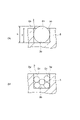
- the ratio of the height of the solder particles S1 to the depth D of the concave portion 3 is not particularly limited, but considering the amount of deformation of the deformable portion 6 in the compression direction, it may be 0.3 to 1.5, for example. By setting the ratio to 0.3 or more, it is possible to more reliably bring the electrode and the solder particles S1 into contact when the electrode is pressed. By setting the ratio to 1.5 or less, it is possible to suitably prevent the solder particles S1 from dropping out of the recesses 3 . In addition, it is possible to prevent the solder particles S1 from protruding from the concave portions 3 during transfer, and to prevent the solder particles S1 from bonding to each other between the adjacent concave portions 3,3.
- the ratio of the height of the solder particles S1 to the depth D of the recesses 3 may be 0.5-1.2, or may be 0.6-1.
- the average particle size of the solder particles S1 is, for example, 35 ⁇ m or less.
- the average particle size of the solder particles S1 may be 30 ⁇ m or less, 25 ⁇ m or less, 20 ⁇ m or less, or 15 ⁇ m or less.
- the average particle size of the solder particles S1 is, for example, 1 ⁇ m or more.
- the average particle size of the solder particles S1 may be 2 ⁇ m or more, 3 ⁇ m or more, or 5 ⁇ m or more.
- FIG. 3 is a schematic cross-sectional view showing an example of the configuration of the connection structure.
- the connection structure 41 is configured by electrically connecting the electrodes 22 of one circuit member 21 and the electrodes 32 of the other circuit member 31 via solder bumps S2.
- the space between one circuit member 21 and the other circuit member 21 is filled with an underfill material 42 whose main ingredient is, for example, epoxy resin.
- the underfill material 42 is formed to cover the electrodes 22 and 32 and the solder bumps S2 between the electrodes 22 and 32, for example.
- connection structure 41 includes connection portions for semiconductor memories, semiconductor logic chips, etc., connection portions for primary and secondary mounting of semiconductor packages, junctions for CMOS image elements, laser elements, LED light emitting elements, and the like. devices such as cameras, sensors, liquid crystal displays, personal computers, mobile phones, smart phones, and tablets using
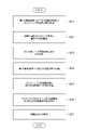
- step S02 the solder particles S1 held in the recesses 3 and the electrodes 22 of the circuit member 21 are arranged to face each other (step S02).
- step S02 the stage 12 is displaced while the circuit member 21 is attracted to the heating and pressurizing head 16, and as shown in FIG. .
- the position of the alignment mark 4 on the side of the solder bump forming member 1 is confirmed by the imaging device 15A, and the position of the alignment mark on the side of the circuit member 21 is confirmed by the imaging device 15B.
- the solder particles S1 and the electrodes 22 of the circuit member 21 are aligned.
- the pressing force of the electrode 22 against the solder bump forming member 1 by the heating and pressurizing head 16 is, for example, 0.1 MPa to 600 MPa.
- This applied pressure may be 1 MPa to 300 MPa, or may be 10 MPa to 100 MPa.
- step S02 or between steps S02 and S03 a step of exposing at least one of the solder particles S1 and the electrodes 22 to a reducing atmosphere may be further included.
- a step of exposing at least one of the solder particles S1 and the electrodes 22 to a reducing atmosphere may be further included.
- the process of step S03 may be performed in a reducing atmosphere.
- hydrogen gas, hydrogen radicals, formic acid gas, etc. can be used to form the reducing atmosphere.
- a hydrogen reduction furnace, a hydrogen reflow furnace, a hydrogen radical furnace, a formic acid furnace, a vacuum furnace of these, a continuous furnace, a conveyor furnace, or the like can be used.
- connection structure 41 is formed.
- the other circuit member 31 is supplied toward the second implementation region R3 (step S04).
- the circuit member 31 is supplied from the third supply unit 17 to the second implementation region R3 so that the electrode 32 faces upward.
- An underfill material 42 may be arranged so as to cover the electrodes 32 in the circuit member 31 supplied to the second implementation region R3.
- step S05 the circuit member 21A with solder bumps and the circuit member 31 are arranged to face each other (step S05).
- step S05 as shown in FIG. 8, the stage 12 is displaced while the circuit member 21A with solder bumps is attracted to the heating and pressurizing head 16, and the circuit member 21A with solder bumps is placed on the second implementation area R3. do.
- the position of the alignment mark on the circuit member 31 side is confirmed by the imaging device 15A, and the position of the alignment mark on the circuit member 21A with solder bumps is confirmed by the imaging device 15B. and the electrode 32 of the circuit member 31 are aligned.
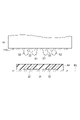
- the deformation portion 6 is deformed in the compression direction by applying heat by pressing the electrode 22, and the electrode 22 of the circuit member 21 contacts the solder particles S1 in a state of entering the recess 3.
- the height of the solder bumps S2 formed on the electrodes 22 can be made uniform within a certain range.
- solder particles S1 are arranged singly in each of the plurality of recesses 3. As a result, the solder particles S1 having a relatively large particle size can be transferred to the electrodes 22 with a certain degree of certainty.
- an alignment mark 4 is provided on the first surface 2a side of the body portion 2 . This facilitates alignment between the solder particles S1 held in the recesses 3 and the electrodes 22 . Therefore, the solder particles S1 can be formed at the target positions on the electrodes 22 with higher accuracy.
- the deformable portion 6 does not extend beyond the depth of the recess 3 from the first surface 2a. It may be provided with a thickness of 1/2 or more of the depth D of the recess 3 in the depth direction. In this case, the deformation portion 6 may be provided with a thickness of 3/5 or more of the depth D of the recess 3 in the depth direction of the recess 3 from the first surface 2a, or a thickness of 4/5 or more. It may be provided at
- none of the solder particles S1 protrude outward from the opening surface of the recess 3, but the present disclosure does not require the heights of the solder particles S1 in the recess 3 to be uniform. Some or all of the solder particles S1 may protrude outward from the opening surface of the recess 3 in order to ensure the transfer of the solder particles S1 to the recess 3 with certainty. That is, as shown in FIG. 11A, the height H of some or all of the solder particles S1 may satisfy H>D with respect to the depth D of the recesses 3 .
Landscapes
- Engineering & Computer Science (AREA)
- Manufacturing & Machinery (AREA)
- Microelectronics & Electronic Packaging (AREA)
- Electric Connection Of Electric Components To Printed Circuits (AREA)
Priority Applications (3)
| Application Number | Priority Date | Filing Date | Title |
|---|---|---|---|
| JP2023532034A JP7831485B2 (ja) | 2021-06-30 | 2022-06-29 | はんだバンプ形成用部材 |
| KR1020247002225A KR20240027706A (ko) | 2021-06-30 | 2022-06-29 | 땜납 범프 형성용 부재 |
| CN202280045732.5A CN117581342A (zh) | 2021-06-30 | 2022-06-29 | 焊料凸块形成用部件 |
Applications Claiming Priority (2)
| Application Number | Priority Date | Filing Date | Title |
|---|---|---|---|
| JP2021-108630 | 2021-06-30 | ||
| JP2021108630 | 2021-06-30 |
Publications (1)
| Publication Number | Publication Date |
|---|---|
| WO2023277085A1 true WO2023277085A1 (ja) | 2023-01-05 |
Family
ID=84691854
Family Applications (1)
| Application Number | Title | Priority Date | Filing Date |
|---|---|---|---|
| PCT/JP2022/026032 Ceased WO2023277085A1 (ja) | 2021-06-30 | 2022-06-29 | はんだバンプ形成用部材 |
Country Status (5)
| Country | Link |
|---|---|
| JP (1) | JP7831485B2 (https=) |
| KR (1) | KR20240027706A (https=) |
| CN (1) | CN117581342A (https=) |
| TW (1) | TW202318605A (https=) |
| WO (1) | WO2023277085A1 (https=) |
Citations (6)
| Publication number | Priority date | Publication date | Assignee | Title |
|---|---|---|---|---|
| JPH08139427A (ja) * | 1994-11-04 | 1996-05-31 | Mitsubishi Electric Corp | 球状電極の形成方法 |
| JPH09246324A (ja) * | 1996-03-08 | 1997-09-19 | Hitachi Ltd | 電子部品及びそのバンプ形成方法 |
| JP2006216702A (ja) * | 2005-02-02 | 2006-08-17 | Tdk Corp | 半田ボールの転写方法及び転写装置 |
| JP2014082362A (ja) * | 2012-10-17 | 2014-05-08 | Mitsubishi Electric Corp | 電子機器の製造方法 |
| JP2016172912A (ja) * | 2015-03-18 | 2016-09-29 | 三菱マテリアル株式会社 | ハンダ粉末の製造方法及びこの粉末を用いたハンダ用ペースト |
| JP2018206953A (ja) * | 2017-06-05 | 2018-12-27 | 三菱マテリアル株式会社 | はんだバンプ形成方法及びはんだペースト |
Family Cites Families (1)
| Publication number | Priority date | Publication date | Assignee | Title |
|---|---|---|---|---|
| JP2017157626A (ja) | 2016-02-29 | 2017-09-07 | 三菱マテリアル株式会社 | はんだバンプの形成方法 |
-
2022
- 2022-06-29 WO PCT/JP2022/026032 patent/WO2023277085A1/ja not_active Ceased
- 2022-06-29 KR KR1020247002225A patent/KR20240027706A/ko active Pending
- 2022-06-29 TW TW111124292A patent/TW202318605A/zh unknown
- 2022-06-29 JP JP2023532034A patent/JP7831485B2/ja active Active
- 2022-06-29 CN CN202280045732.5A patent/CN117581342A/zh active Pending
Patent Citations (6)
| Publication number | Priority date | Publication date | Assignee | Title |
|---|---|---|---|---|
| JPH08139427A (ja) * | 1994-11-04 | 1996-05-31 | Mitsubishi Electric Corp | 球状電極の形成方法 |
| JPH09246324A (ja) * | 1996-03-08 | 1997-09-19 | Hitachi Ltd | 電子部品及びそのバンプ形成方法 |
| JP2006216702A (ja) * | 2005-02-02 | 2006-08-17 | Tdk Corp | 半田ボールの転写方法及び転写装置 |
| JP2014082362A (ja) * | 2012-10-17 | 2014-05-08 | Mitsubishi Electric Corp | 電子機器の製造方法 |
| JP2016172912A (ja) * | 2015-03-18 | 2016-09-29 | 三菱マテリアル株式会社 | ハンダ粉末の製造方法及びこの粉末を用いたハンダ用ペースト |
| JP2018206953A (ja) * | 2017-06-05 | 2018-12-27 | 三菱マテリアル株式会社 | はんだバンプ形成方法及びはんだペースト |
Also Published As
| Publication number | Publication date |
|---|---|
| KR20240027706A (ko) | 2024-03-04 |
| CN117581342A (zh) | 2024-02-20 |
| JP7831485B2 (ja) | 2026-03-17 |
| TW202318605A (zh) | 2023-05-01 |
| JPWO2023277085A1 (https=) | 2023-01-05 |
Similar Documents
| Publication | Publication Date | Title |
|---|---|---|
| US6221691B1 (en) | Method and system for attaching semiconductor dice to substrates | |
| US7726546B2 (en) | Bonding apparatus and bonding method | |
| JP7697292B2 (ja) | はんだバンプ形成装置 | |
| KR100203603B1 (ko) | 칩 크기의 패키지형 반도체 장치의 제조 방법 | |
| US20090302095A1 (en) | Techniques for arranging solder balls and forming bumps | |
| US20160148965A1 (en) | Detector assembly using vertical wire bonds and compression decals | |
| CN1194059A (zh) | 用于粘合电子器件的可变形基片部件 | |
| KR102924379B1 (ko) | 땜납 범프 형성용 부재, 땜납 범프 형성용 부재의 제조 방법, 및 땜납 범프 부착 전극 기판의 제조 방법 | |
| JP3305162B2 (ja) | はんだバンプ形成方法及び装置 | |
| JP7831485B2 (ja) | はんだバンプ形成用部材 | |
| JP7831484B2 (ja) | はんだバンプ形成方法 | |
| KR102325868B1 (ko) | 언더필재, 언더필 필름, 및 이를 이용한 반도체 장치의 제조 방법 | |
| TW202321040A (zh) | 連接結構體之製造方法 | |
| JP2023046305A (ja) | 接続構造体の製造方法 | |
| US11270968B2 (en) | Electronic circuit connection method and electronic circuit | |
| Chen et al. | High-Speed Precision Handling Technology of Micro-Chip for Fan-Out Wafer Level Packaging (FOWLP) Application | |
| Li et al. | Review on Fan-Out Packaging of Light-Emitting Diodes: Process Route, Manufacturing Reliability, and Performance Optimization | |
| JP7841437B2 (ja) | はんだバンプ付き部材の製造方法、及びはんだバンプ形成用部材 | |
| JP2023050157A (ja) | フィラー含有フィルム | |
| CN119852201A (zh) | 封装设备、封装制程及压平装置 | |
| KR20240139656A (ko) | 기둥형 접속체의 기판 본딩 방법 | |
| JPH10321678A (ja) | 導電粒子配列方法及び導電粒子配列テープ | |
| Chang et al. | GGI technology for the application of low profile image sensor module | |
| JP2003086632A (ja) | 半導体装置及びその製造方法並びに封止用樹脂 | |
| JP2003203938A (ja) | チップ状電子部品の製造方法、並びにその製造に用いる疑似ウェーハの製造方法 |
Legal Events
| Date | Code | Title | Description |
|---|---|---|---|
| 121 | Ep: the epo has been informed by wipo that ep was designated in this application |
Ref document number: 22833231 Country of ref document: EP Kind code of ref document: A1 |
|
| WWE | Wipo information: entry into national phase |
Ref document number: 2023532034 Country of ref document: JP |
|
| WWE | Wipo information: entry into national phase |
Ref document number: 202280045732.5 Country of ref document: CN |
|
| ENP | Entry into the national phase |
Ref document number: 20247002225 Country of ref document: KR Kind code of ref document: A |
|
| NENP | Non-entry into the national phase |
Ref country code: DE |
|
| 122 | Ep: pct application non-entry in european phase |
Ref document number: 22833231 Country of ref document: EP Kind code of ref document: A1 |