WO2023276982A1 - 液滴センサー、結露検出装置およびそれらの製造方法 - Google Patents
液滴センサー、結露検出装置およびそれらの製造方法 Download PDFInfo
- Publication number
- WO2023276982A1 WO2023276982A1 PCT/JP2022/025639 JP2022025639W WO2023276982A1 WO 2023276982 A1 WO2023276982 A1 WO 2023276982A1 JP 2022025639 W JP2022025639 W JP 2022025639W WO 2023276982 A1 WO2023276982 A1 WO 2023276982A1
- Authority
- WO
- WIPO (PCT)
- Prior art keywords
- platinum
- metal
- electrode
- containing material
- layer
- Prior art date
- Legal status (The legal status is an assumption and is not a legal conclusion. Google has not performed a legal analysis and makes no representation as to the accuracy of the status listed.)
- Ceased
Links
Images







Classifications
-
- G—PHYSICS
- G01—MEASURING; TESTING
- G01N—INVESTIGATING OR ANALYSING MATERIALS BY DETERMINING THEIR CHEMICAL OR PHYSICAL PROPERTIES
- G01N27/00—Investigating or analysing materials by the use of electric, electrochemical, or magnetic means
- G01N27/26—Investigating or analysing materials by the use of electric, electrochemical, or magnetic means by investigating electrochemical variables; by using electrolysis or electrophoresis
- G01N27/403—Cells and electrode assemblies
- G01N27/4035—Combination of a single ion-sensing electrode and a single reference electrode
-
- G—PHYSICS
- G01—MEASURING; TESTING
- G01N—INVESTIGATING OR ANALYSING MATERIALS BY DETERMINING THEIR CHEMICAL OR PHYSICAL PROPERTIES
- G01N27/00—Investigating or analysing materials by the use of electric, electrochemical, or magnetic means
- G01N27/02—Investigating or analysing materials by the use of electric, electrochemical, or magnetic means by investigating impedance
- G01N27/04—Investigating or analysing materials by the use of electric, electrochemical, or magnetic means by investigating impedance by investigating resistance
- G01N27/06—Investigating or analysing materials by the use of electric, electrochemical, or magnetic means by investigating impedance by investigating resistance of a liquid
-
- G—PHYSICS
- G03—PHOTOGRAPHY; CINEMATOGRAPHY; ANALOGOUS TECHNIQUES USING WAVES OTHER THAN OPTICAL WAVES; ELECTROGRAPHY; HOLOGRAPHY
- G03F—PHOTOMECHANICAL PRODUCTION OF TEXTURED OR PATTERNED SURFACES, e.g. FOR PRINTING, FOR PROCESSING OF SEMICONDUCTOR DEVICES; MATERIALS THEREFOR; ORIGINALS THEREFOR; APPARATUS SPECIALLY ADAPTED THEREFOR
- G03F7/00—Photomechanical, e.g. photolithographic, production of textured or patterned surfaces, e.g. printing surfaces; Materials therefor, e.g. comprising photoresists; Apparatus specially adapted therefor
- G03F7/16—Coating processes; Apparatus therefor
- G03F7/161—Coating processes; Apparatus therefor using a previously coated surface, e.g. by stamping or by transfer lamination
-
- G—PHYSICS
- G03—PHOTOGRAPHY; CINEMATOGRAPHY; ANALOGOUS TECHNIQUES USING WAVES OTHER THAN OPTICAL WAVES; ELECTROGRAPHY; HOLOGRAPHY
- G03F—PHOTOMECHANICAL PRODUCTION OF TEXTURED OR PATTERNED SURFACES, e.g. FOR PRINTING, FOR PROCESSING OF SEMICONDUCTOR DEVICES; MATERIALS THEREFOR; ORIGINALS THEREFOR; APPARATUS SPECIALLY ADAPTED THEREFOR
- G03F7/00—Photomechanical, e.g. photolithographic, production of textured or patterned surfaces, e.g. printing surfaces; Materials therefor, e.g. comprising photoresists; Apparatus specially adapted therefor
- G03F7/16—Coating processes; Apparatus therefor
- G03F7/164—Coating processes; Apparatus therefor using electric, electrostatic or magnetic means; powder coating
-
- G—PHYSICS
- G01—MEASURING; TESTING
- G01N—INVESTIGATING OR ANALYSING MATERIALS BY DETERMINING THEIR CHEMICAL OR PHYSICAL PROPERTIES
- G01N27/00—Investigating or analysing materials by the use of electric, electrochemical, or magnetic means
- G01N27/26—Investigating or analysing materials by the use of electric, electrochemical, or magnetic means by investigating electrochemical variables; by using electrolysis or electrophoresis
- G01N27/28—Electrolytic cell components
- G01N27/30—Electrodes, e.g. test electrodes; Half-cells
Definitions
- the present invention relates to a droplet sensor and a condensation detection device, and more particularly to a droplet sensor, a condensation detection device, and a manufacturing method thereof with high droplet detection accuracy and sensitivity.
- Droplet sensors and dew condensation detectors that use them include elements that measure changes in electrical resistance (impedance) and capacitance of sensor elements, as well as galvanic sensors that flow between two metals via droplets. Elements that sense current (galvanic droplet sensors) are known. Among these, the galvanic droplet sensor has many features such as simple structure, compact size, high droplet detection sensitivity, and ability to operate without necessarily requiring an external power source.
- This galvanic droplet sensor has a structure in which a large number of wires using two different metals are arranged at minute intervals. Droplets are detected by sensing the current flowing between the wires.
- This galvanic droplet sensor is disclosed, for example, in Patent Document 1.
- Non-Patent Document 1 proposes that in a galvanic droplet sensor using aluminum/gold as a combination of dissimilar metals, the electrical output is increased by coating the cathode gold with platinum.
- condensation occurs on the surface of an object, it can cause mold and rust and scatter light.
- the wall material and contaminants adhering to the surface thereof are often used as nutrients to generate mold, and in the case of metal, rust is generated due to corrosion.
- Condensation in the pantry degrades the taste and quality of food.
- hygienic problems such as mold becoming more likely to occur in food, are more likely to occur.
- fogging occurs when dew condensation occurs on a transparent member such as a window glass. If dew condensation occurs on the lens due to high humidity or the like, the light incident on the lens is scattered, resulting in deterioration of the imaging performance of the lens such as distortion of the image.
- the object of the present invention is to solve these conventional problems, reduce manufacturing variations (variation due to the manufacturing process) between droplet sensors and dew condensation detection devices even when manufactured in large quantities, and achieve high detection accuracy.
- An object of the present invention is to provide a liquid droplet sensor and a dew condensation detection device capable of obtaining a high electrical output and having stable detection characteristics, and a manufacturing method thereof.
- (Configuration 1) an insulating substrate; a first electrode having a first thin wire and a first current collector; A second electrode having a second thin wire and a second current collector, The first electrode and the second electrode are arranged on the insulating substrate, and the first fine lines and the second fine lines are alternately arranged on the insulating substrate, A droplet sensor for sensing a galvanic current flowing through a conductive droplet between the first thin wire and the second thin wire, The first fine wire and the first current collector are composed of a first metal-containing layer having an electrical resistivity lower than that of platinum, The second thin wire is composed of a composite film of the first metal-containing material layer and a platinum-containing material layer made of platinum or a platinum alloy, and the second current collector is the first metal-containing material layer.
- a droplet sensor wherein at least a portion of the surface of the platinum-containing material layer is exposed to the outside.
- Configuration 2 The droplet sensor according to configuration 1, wherein the second thin wire is formed of a laminated film of the first metal-containing material layer and the platinum-containing material layer.
- Composition 3 The liquid droplet sensor according to configuration 1, wherein the second fine wire has a core portion made of the first metal-containing material layer, and the platinum-containing material layer is formed on at least a part of a side wall portion of the core portion. .
- Composition 4 The liquid droplet sensor according to configuration 1, wherein the second fine wire has a core portion formed of the first metal-containing material layer, and the platinum-containing material layer is formed so as to cover the core portion.
- Composition 5 5.
- a drop sensor according to any one of the configurations 1-4, wherein the spacing between the first thin line and the second thin line is constant.
- the first metal inclusion layer includes aluminum (Al), magnesium (Mg), zinc (Zn), iron (Fe), cobalt (Co), nickel (Ni), molybdenum (Mo), copper (Cu), 6. Any one of configurations 1 to 5, which is made of one or more metals selected from the group consisting of silver (Ag), gold (Au), and tungsten (W), or an alloy containing one or more metals selected from the group. Droplet sensor. (Composition 7) 7. The drop sensor of any one of configurations 1-6, wherein the platinum-containing layer has a thickness of 5 nm to 150 nm.
- composition 8 The droplet sensor according to any one of configurations 1 to 7, wherein the distance between the first thin line and the second thin line is 100 nm or more and 100 ⁇ m or less.
- composition 9 The droplet sensor of configuration 8, wherein the spacing between the first thin line and the second thin line is 100 nm or more and 10 ⁇ m or less.
- Configuration 10 A dew condensation detection device equipped with the droplet sensor according to any one of Structures 1 to 9.
- composition 11 preparing an intermediate structure having a pattern formed of a platinum-containing material layer made of platinum or a platinum alloy on an insulating substrate; forming a first metal inclusion layer containing a metal having an electrical resistivity lower than that of platinum on the intermediate structure; A first fine line comprising the first metal-containing layer and a first current collector comprising the first metal-containing layer on the insulating substrate using one lithography. and a second current collector comprising a second fine wire made of a composite film of the platinum-containing material layer and the first metal-containing material layer and the first metal-containing material layer and alternately juxtaposing said first fine lines and said second fine lines on said insulating substrate.
- Composition 12 forming a first metal inclusion layer containing a metal having an electrical resistivity lower than that of platinum on an insulating substrate; producing an intermediate structure having a pattern formed of a laminate in which a platinum-containing material layer made of platinum or a platinum alloy is laminated on the first metal-containing material layer; A first fine line comprising the first metal-containing layer and a first current collector comprising the first metal-containing layer on the insulating substrate using one lithography. and a second current collector comprising a second fine wire made of a composite film of the platinum-containing material layer and the first metal-containing material layer and the first metal-containing material layer and alternately juxtaposing said first fine lines and said second fine lines on said insulating substrate.
- composition 13 A first fine wire comprising a first metal-containing layer containing a metal having an electrical resistivity lower than that of platinum and a first current collector comprising the first metal-containing layer on an insulating substrate. and a second current collector comprising a second thin wire made of a composite film of the first metal-containing layer and a platinum-containing layer made of platinum or a platinum alloy and the first metal-containing layer.
- a method for manufacturing a droplet sensor or a condensation detection device in which a second electrode having a A temporary electrode comprising the first electrode and the first metal-containing material layer on the insulating substrate, and having the same pattern as the second electrode or a pattern obtained by subjecting the pattern of the second electrode to a resin treatment.
- composition 14 14. The method of manufacturing a droplet sensor or condensation detection device according to configuration 13, wherein the first electrode and the temporary electrode are formed by a single lift-off process.
- Composition 15 14. The drop sensor of configuration 13, wherein the first electrode and the temporary electrode are formed by one deposition, one lithography and etching of the first metal inclusion on the insulating substrate. Or a manufacturing method of a dew condensation detection device.
- Composition 16 A first fine wire comprising a first gold metal-containing layer containing a metal having an electrical resistivity lower than that of platinum and a first current collector comprising the first metal-containing layer on an insulating substrate. a second current collector comprising one electrode, a second fine wire comprising a composite film of said first metal-containing material layer and a platinum-containing material layer made of platinum or a platinum alloy, and said first metal-containing material layer.
- a method for manufacturing a droplet sensor or a condensation detection device in which a second electrode having sequentially forming the first metal-containing layer and an oxide insulating film on the insulating substrate; Forming on the insulating substrate a temporary electrode having the same pattern as the first electrode and the second electrode or a pattern obtained by lacquering the pattern of the second electrode, including a single lithography process.
- a droplet sensor or dew condensation detection device according to configuration 16, wherein the oxide insulating film is made of an oxide containing one or more substances selected from the group consisting of yttrium (Y), aluminum, silicon (Si), and cerium (Ce). manufacturing method.
- the first metal inclusion layer contains one or more metals selected from the group consisting of aluminum, magnesium, zinc, iron, cobalt, nickel, molybdenum, copper, silver, gold, and tungsten, or one metal selected from the group. 18.
- a method of manufacturing a liquid drop sensor or a dew condensation detection device according to any one of structures 11 to 17, which is made of the alloy containing the above. (Composition 19) 19.
- a liquid droplet sensor and a dew condensation detection device having stable detection characteristics with little manufacturing variation between elements even when manufactured in large quantities, high detection accuracy, high electrical output, and manufacturing thereof A method is provided.
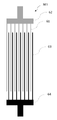
- FIG. 3 is a bird's-eye view for explaining the configuration and operation of a galvanic droplet sensor 201.
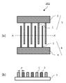
- FIG. It is a figure which shows the principal part structure of the galvanic droplet sensor 201, (a) is a top view, (b) is sectional drawing.
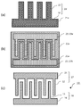
- FIG. 4 is a top view illustrating one of the problems of conventional galvanic droplet sensors.
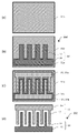
- 1 is a cross-sectional view for explaining the configuration of a main part of a galvanic liquid droplet sensor of the present invention;
- FIG. It is a manufacturing process diagram showing a manufacturing process of the first galvanic liquid droplet sensor 101 of the present invention in a cross-sectional view.
- 2 is a manufacturing process diagram showing a manufacturing process of the first galvanic liquid droplet sensor 101 of the present invention in plan view. It is a manufacturing process drawing which showed the manufacturing process of the 2nd galvanic droplet sensor 102 of this invention by sectional drawing. It is a manufacturing process diagram showing a manufacturing process of the second galvanic liquid droplet sensor 102 of the present invention in plan view. It is a manufacturing process drawing which showed the manufacturing process of the 3rd galvanic type liquid droplet sensor 103 of this invention with the sectional view. It is a manufacturing process drawing which showed the manufacturing process of the 3rd galvanic type droplet sensor 103 of this invention with the planar view.
- FIG. 10 is a plan view illustrating the configuration of a sample before Pt plating treatment in Example 2;
- the upper surface of the sample before Pt plating (the portion containing the first thin wire and the first current collector) was observed with an optical microscope (left side), and the first thin wire and the first collector.
- the photograph (right side) which observed the upper surface of the sample after performing Pt-plating process with respect to the Al layer which comprises an electric body with the optical microscope.
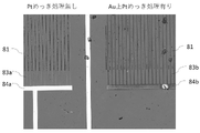
- Example 2 the upper surface of the sample before Pt plating (the portion containing the second thin wire and the second current collector) was observed with an optical microscope (left side), and the second thin wire and the second collector.
- FIG. 4 is a photograph (right side) of the upper surface of a sample observed with an optical microscope after Pt plating treatment was performed on an Au layer that constitutes an electric body.
- the galvanic droplet sensor 201 As shown in FIG. 1, thin wires made of different metals (metals A and B) are arranged side by side on an insulating substrate. It is a current detection type sensor that utilizes the phenomenon that a galvanic current flows between thin wires when a conductive liquid droplet such as a water droplet touches the thin wire.
- the electrode 202 of the galvanic droplet sensor 201 includes, as shown in FIG. 1 electrode 5 ), and a second thin wire 2 and a second current collector 4 electrically connected to the second thin wire 2 (these are also collectively referred to as a second electrode 6 ). ).
- the metal forming the first fine wire 1 is different from the metal forming the second fine wire 2 .
- the first fine wire 1 and the first current collector 3, and the second fine wire 2 and the second current collector 4 are made of the same material in terms of wiring fabrication. From the point of view, it is preferable that the first current collector 3 and the second current collector 4 are made of the same material, and that the wiring drawn out from the galvanic droplet sensor 201 is also made of the same material.
- 2(a) is a top view
- (b) is a cross-sectional view taken along line AA' in FIG. 2(a)
- 7 is an insulating substrate
- d is a first substrate. 1 and a second thin line 2.
- FIG. 3 shows the pattern 202a of the electrodes (thin wires and collectors) of the galvanic droplet sensor 201 viewed from above.
- the design interval d is 1 ⁇ m, it is necessary to allow misalignment of 0.2 to 0.25 ⁇ m.
- the galvanic droplet sensor 201 detects that a droplet has come into contact with the first fine wire 1 and the second fine wire 2, the distance d between the first fine wire 1 and the second fine wire 2 is , directly governs the size of the droplets to be detected. Therefore, the accuracy of the spacing d is extremely important for the galvanic droplet sensor 201 . Such a large misalignment as described above is unacceptable, and it is necessary to select those whose distance d is within the allowable range, resulting in a low product yield.
- FIG. 4 shows the structure of the thin wires forming the liquid drop detector, which is the main part of the galvanic liquid drop sensor according to the embodiment of the present invention. Its structure can be broadly divided into four types of first to fourth galvanic droplet sensors 101 to 104 shown in FIGS. 4(a) to 4(d). It consists of a first metal-containing layer with a low electrical resistivity, and the second fine wire is a composite film of the first metal-containing layer and a platinum-containing layer such as platinum or a platinum alloy. Although not shown in FIG. 4, in the first to fourth galvanic droplet sensors 101 to 104, the first current collector is composed of the first metal-containing layer, and the second current collector is composed of the first metal-containing layer.
- the electrical body includes the first metal inclusion layer.
- the second thin line is formed so that at least part of the surface of the platinum-containing material layer that constitutes the composite film is exposed to the outside, and the exposed part can be contacted by a conductive droplet.
- “exposed to the outside” means that the droplet to be detected is in an environment where it can come into contact, and limits whether the space in which the droplet sensor itself is placed is an open system or a closed system. Note that it does not
- the arrangement of the first fine lines 12 and the second fine lines 13 is determined by one lithography process.
- the distances d1 and d2 between the first fine line 12 and the second fine line 13 can be the same value. Therefore, it is possible to prevent a drop in droplet detection accuracy due to variations in fine line spacing.
- the second thin wire 13 has a layer made of a platinum-containing material such as platinum or a platinum alloy that produces a high galvanic effect (high electromotive current), and is an electrical conductor with a lower resistivity than platinum.
- the galvanic current that flows when the conductive droplet straddles between the first thin wire 12 and the second thin wire 13 increases. Therefore, the droplet detection sensitivity of the droplet sensor can be enhanced.
- the first and second current collectors which correspond to the first current collector 3 and the second current collector 4 in the electrodes of the conventional galvanic droplet sensor, can also be manufactured in the second method without going through a special process. It is also possible to use one type of material for the output terminal of the droplet sensor. Therefore, it is also possible to avoid contact potential problems when connecting the droplet sensor to other equipment such as amplifiers, analysis, and alarm devices.
- the first metal inclusions include aluminum (Al), magnesium (Mg), zinc (Zn), iron (Fe), cobalt (Co), nickel (Ni), molybdenum (Mo), copper (Cu ), silver (Ag), gold (Au), and tungsten (W), or an alloy containing one or more metals selected from the group.
- Al has a low electric resistance, is easy to process, is widely used, and can be used particularly favorably because of its low material and process costs.
- Al alloys include Al--Cu, Al--Si, Al--Cu--Si, Al--Mn, Al--Mg, Al--Mg--Si, Al--Mg--Zn and Al--Mg--Zn--Cu.
- platinum alloys include Pt--Au, Pt--Pd, Pt--Ir, Pt--Rh, Pt--Co, Pt--Fe and Pt--Cr.
- the structure of the first galvanic droplet sensor 101 is, as shown in FIG. 1 thin wire 12, and a second thin wire 13 having a two-layer film of an upper layer 13a made of the same material as the first thin wire 12 and a lower layer 13b made of a platinum-containing material.
- the lower layer of the second thin wire is composed of a platinum-containing material, droplets accumulate at the bottom of the space between the thin wires (the droplet is on the insulating substrate and straddles the thin wires). It is characterized by being able to detect droplets even if the amount is very small.
- the first thin wire 12 is electrically connected to the first current collector
- the second thin wire 13 is electrically connected to the second current collector
- the first and second current collectors are , is connected to a signal output terminal via an electric wiring (not shown) connected thereto.
- an amplifier may be connected to the first current collector and the second current collector to amplify the galvanic current that flows due to the presence of the droplet.
- a galvanic current flows when a conductive droplet, such as a water droplet, is connected between a first metal and a second metal having a different electrochemical potential.
- Water has low conductivity and is insulating in the state of ultrapure water. sensing) possible galvanic current flows.
- both thin wires are close to each other with respect to the area of the droplet detection portion (area where the first electrode and the second electrode are arranged) on the substrate. can be lengthened.
- parallel running distance the length of the adjacent portion between the thin wires
- a comb structure or a double spiral structure can be mentioned. Since the structure itself for maximizing the parallel running distance of two thin wires within a certain plane area is well known in the field of semiconductor devices and the like, such a structure may also be adopted as necessary.
- "arranging fine lines side by side on a substrate” does not specify the mutual orientation of a plurality of fine lines placed on the substrate, but arranging the fine lines on the same plane of the substrate so as to be spaced apart from each other. Say things.
- the structure of the second galvanic droplet sensor 102 is obtained by reversing the lamination order of the laminated films of the second thin wire 13 of the first galvanic droplet sensor 101.
- a first thin wire 12 formed on an insulating substrate 11 and made of a first metal-containing material layer having an electrical resistivity lower than that of platinum; an upper layer 13b made of a platinum-containing material;
- the second thin wire 13 is a two-layered film 13a made of the same material as the second fine wire 13. As shown in FIG.
- the upper layer of the second thin wire is composed of a platinum-containing material
- the first In addition to enhancing the galvanic effect due to the platinum-containing material that is the upper layer of the thin wire in 2, the current is increased due to the low electrical resistance of the first metal-containing material that is the lower layer (that is, the upper layer is separated from the first metal-containing material that constitutes the lower layer. sufficient current is supplied to the constituent platinum-containing material) can be obtained at the same time.
- the structure of the third galvanic droplet sensor 103 is, as shown in FIG. 1 thin wire 12, a core portion (base layer) 13a made of the same material as the first thin wire 12, and a second composite film 13b made of a platinum-containing material layer formed so as to cover the core portion. It consists of thin wires 13 .
- This structure has a structure in which all the portions of the second fine wire 13 exposed to the outside are made of a platinum-containing material, and the electric resistance can be greatly reduced by the first metal-containing material in the core portion, so that the electric resistance is high. It is characterized in that droplet detection sensitivity can be stably obtained.
- the structure of the fourth galvanic droplet sensor 104 is, as shown in FIG.
- It is composed of a second fine wire 13 which is a composite film of an oxide insulating film 14 formed as a cap on the upper surface and an oxide insulating film 13b made of a material layer.
- the oxide insulating film 14 has an etching mask function when etching the first metal-containing layer in manufacturing the sensor, a protective cap function for protecting the first and second fine lines, and a protective cap function for protecting the first and second fine lines.
- the upper surface is made insulative, and the path through which the galvanic current flows is limited to the side wall portions of the first and second thin wires, thereby providing a steep characteristic function of sharpening the detection response depending on the droplet size.
- the oxide insulating film 14 with a hydrophobic or hydrophilic material to control droplet wettability, it is possible to have a detection characteristic control function of improving the detection response depending on the droplet size.
- the material of the oxide insulating film 14 is not particularly limited as long as it has the above function, but at least one substance selected from the group consisting of yttrium (Y), aluminum, silicon (Si), and cerium (Ce) is used.
- Oxide containing, in particular Y 2 O 3 , Al 2 O 3 , SiO 2 , CeO 2 can be used with particular preference.
- the detection response (current-time curve) depending on the droplet size becomes steep, and it is characterized in that the size of the droplet to be detected can be easily specified.
- the distances d 1 and d 2 are constant values, the measured values of the distances d 1 and d 2 are completely the same. Not limited.
- the fact that the interval between the first fine line 12 and the second fine line 13 is constant is not limited to the case where the interval between the first fine line 12 and the second fine line 13 is completely the same. It includes errors due to the measurement accuracy (reproducibility) of equipment such as CD-SEM (length-measuring SEM).
- the droplet detection unit on the insulating substrate 11 (the first thin wire 12 and the first electrode having the first current collector, The distance between the first thin wire 12 and the second thin wire 13 in the region where the second thin wire 13 and the second electrode having the second current collector are arranged) is preferably 100 nm or more and 100 ⁇ m or less, It is more preferably 100 nm or more and 10 ⁇ m or less. Within this range, droplets can be detected with high sensitivity. Moreover, the thickness of the platinum-containing layer 13b is preferably 5 nm or more and 150 nm or less.
- the thickness of the platinum-containing material layer 13b is 5 nm or more, it is easy to ensure the uniformity of the thickness of the platinum-containing material layer during sensor manufacturing, and there are few places where the platinum-containing material layer is not formed, that is, so-called defective portions. As a result, it is possible to obtain high droplet detection accuracy. Further, by setting the thickness of the platinum-containing material layer 13b to 150 nm or less, the proportion of the first metal-containing material having relatively lower electrical resistivity than that of the platinum-containing material in the second thin wire is increased. It becomes possible to easily lower the electrical resistance of the thin wire of Also, it is possible to reduce the amount of expensive platinum used. Since the galvanic droplet sensor is a current detection sensor, it is extremely important to reduce the electrical resistance of the part that detects the contact of droplets in order to obtain high droplet detection sensitivity.
- FIG. 5 is a cross-sectional view
- FIG. 6 which is a plan view.
- the insulating substrate 11 is prepared, the pattern 21a of the platinum-containing material layer is formed on the insulating substrate 11, and the intermediate structure 111 is produced (see FIG. 5A).
- a substrate having an SiO2 oxide film formed on a Si wafer a glass substrate such as synthetic quartz glass, soda lime glass, acrylic, polystyrene (PS), polypropylene (PP), polyethylene terephthalate, etc. (PET), polycarbonate (PC), etc., and resin layers such as acrylic resin, methacrylate resin, novolac resin, polyester resin, polyamide resin, polyimide resin, polyamide-imide resin, silicone resin, etc. are formed on these substrates.
- a formed substrate may be mentioned.
- the pattern 21a of the platinum-containing material layer is a pattern obtained by broadening the pattern of the second electrode 18 in which the second fine wire 13 and the second current collector 16 to be finally formed are integrated (Fig. 6(a)).
- the amount of broadening may be determined in consideration of the misalignment amount between lithography.
- a method for forming the pattern 21a of the platinum-containing material layer a method comprising forming a thin film of a platinum-containing material such as Pt, lithography and etching, and a lift-off method can be used. Examples of methods for forming a platinum-containing thin film include a sputtering method, a vapor deposition method, a CVD (Chemical Vapor Deposition) method, and a coating method.
- a first metal inclusion constituting a first electrode in which the first fine wire and the first collector are integrated is deposited, and the first metal inclusion is deposited on the intermediate structure 111.
- a layer 22a is formed (see FIG. 5(b)).
- Al can be used as the first metal inclusion.
- the method for depositing the first metal-containing substance includes a sputtering method, a vapor deposition method, and a CVD method.
- a resist pattern 23 including a resist pattern 23b of the second electrode 18 is formed by one exposure (see FIGS. 5C and 6B).
- the first metal-containing material layer 22a is etched to form the pattern 22 of the first metal-containing material layer (see FIG. 5(d)).
- the pattern 21a of the platinum-containing material layer is also etched to form the pattern 21 of the platinum-containing material layer (see FIG. 5(e)).
- the etching gas when Al is used as the first metal-containing material, a chlorine-, bromine-, or iodine-based gas can be used.
- the resist pattern 23 is removed by ashing or stripping solution to form a first electrode 17 having a first fine wire 12 and a first current collector 15, and a second fine wire 13 and a second current collector.
- a first galvanic drop sensor 101 with a second electrode 18 having 16 is fabricated (see FIGS. 5(f) and 6(c)).
- the first fine lines 12 are configured as part of the pattern 22 of the first metal inclusion layer and the second fine lines 13 are part (13a) of the pattern 22 of the first metal inclusion layer. and part of the platinum-containing material layer pattern 21 consisting of the platinum-containing material layer (13b).
- a first current collector 15 having the same configuration as the first fine wire 12 and a second current collector 16 having the same configuration as the second fine wire 13 can be formed at the same time. That is, in this method, the first electrode 17 is formed by integrating the first fine wire 12 and the first collector 15, and the second electrode 17 is formed by combining the second fine wire 13 and the second collector 16. The area where the two electrodes 18 are formed and where the first electrode 17 and the second electrode 18 are formed constitutes a droplet detection portion of the first galvanic droplet sensor 101 .
- the arrangement of the first fine wire 12 and the second fine wire 13 (that is, the arrangement of the first electrode 17 and the second electrode 18) is one. Since it is determined by the resist pattern 23 formed by one exposure, the difference ⁇ d between the distances d1 and d2 between the first thin line 12 and the second thin line 13 can be made zero. Therefore, it is possible to prevent drop detection accuracy from deteriorating due to variations in fine line spacing.
- the second current collector 16 has the same configuration as the configuration of the second fine wire 13, the upper layer is composed of the first metal-containing layer, and is the same material as the first current collector 15. Therefore, the wiring drawn out from the first galvanic droplet sensor 101 can be made of the same material. Therefore, the first galvanic droplet sensor 101 manufactured by this method has a preferable structure from the viewpoint of electrical resistance as described above.
- FIG. 7 is a cross-sectional view
- FIG. 8 which is a plan view.
- the insulating substrate 11 is prepared, and a first metal inclusion layer 31a is formed by depositing a first metal inclusion layer 31a, such as Al, having an electrical resistivity lower than that of platinum on the insulating substrate 11 ( 7(a) and 8(a)).
- a first metal inclusion layer 31a such as Al
- the same one as described in the manufacturing method of the first structure can be used.
- the method for depositing the first metal-containing substance include a sputtering method, a vapor deposition method, and a CVD method.
- a platinum-containing material layer pattern 32a made of a platinum-containing material is formed (laminated) to fabricate the intermediate structure 112 (FIGS. 7B and 8).
- the pattern 32a of the platinum-containing material layer is a pattern obtained by broadening the pattern of the second electrode 18 in which the second thin wire 13 and the second current collector 16 to be finally formed are integrated (Fig. 8(b)).
- the amount of broadening may be determined in consideration of the misalignment amount between lithography.
- a method for forming the pattern 32a of the platinum-containing material layer a method comprising forming a thin film of a platinum-containing material such as Pt, lithography and etching, and a lift-off method can be used.
- methods for forming a platinum-containing thin film include a sputtering method, a vapor deposition method, a CVD method, a coating method, and a plating method.
- a resist pattern 33 including the resist pattern 33b of the second electrode 18 is formed by one exposure (see FIGS. 7C and 8C).
- the pattern 32a of the platinum-containing material layer and the first metal-containing material layer 31a are etched to remove the pattern 32 of the platinum-containing material layer and the pattern 31 of the first metal-containing material layer. forming (see FIG. 7(d)).
- the etching gas when Al is used as the first metal-containing material, a chlorine-, bromine-, or iodine-based gas can be used.
- the resist pattern 33 is removed by ashing or a stripping solution to form a first electrode 17 having a first thin line 12 and a first current collector 15, and a second thin line 13 and a second current collector.
- a second galvanic drop sensor 102 with a second electrode 18 having 16 is fabricated (see FIGS. 7(e) and 8(d)).
- the first fine lines 12 are configured as part of the pattern 31 of the first metal inclusion layer
- the second fine lines 13 are part (13a) of the pattern 31 of the first metal inclusion layer.
- part of the platinum-containing material layer pattern 32 consisting of the platinum-containing material layer (13b).
- a first current collector 15 having the same configuration as the first fine wire 12 and a second current collector 16 having the same configuration as the second fine wire 13 can be formed at the same time. That is, in this method, the first electrode 17 is formed by integrating the first fine wire 12 and the first collector 15, and the second electrode 17 is formed by combining the second fine wire 13 and the second collector 16. The area where the two electrodes 18 are formed and where the first electrode 17 and the second electrode 18 are formed constitutes a droplet detection portion of the second galvanic droplet sensor 102 .
- the arrangement of the first fine wire 12 and the second fine wire 13 (that is, the arrangement of the first electrode 17 and the second electrode 18) is one. Since it is determined by the resist pattern 33 formed by one exposure, the difference ⁇ d between the distances d1 and d2 between the first thin line 12 and the second thin line 13 can be made zero. Therefore, it is possible to prevent drop detection accuracy from deteriorating due to variations in fine line spacing.
- the second current collector 16 has the same configuration as the configuration of the second fine wire 13, the lower layer is the first metal-containing layer, and is the same material as the first current collector 15. Therefore, the wiring drawn out from the second galvanic droplet sensor 102 can be made of the same material. Therefore, the second galvanic droplet sensor 102 manufactured by this method has a preferable structure from the viewpoint of electrical resistance as described above.
- FIG. 9 is a cross-sectional view
- FIG. 10 which is a plan view.
- an insulating substrate 11 is prepared, and a first metal inclusion layer 41a is formed by depositing a first metal inclusion layer 41a, such as Al, having an electrical resistivity lower than that of platinum on the insulating substrate 11 ( See FIG. 9(a)).
- a first metal inclusion layer 41a such as Al
- the same one as described in the manufacturing method of the first structure can be used.
- the method for depositing the first metal-containing substance include a sputtering method, a vapor deposition method, and a CVD method.
- the resist pattern 43 includes a resist pattern 43b having a pattern obtained by subjecting the pattern of the second electrode 18 in which the second fine line 13 and the second current collector 16 to be finally formed are subjected to a resin treatment, and a resist pattern 43b.
- a resist pattern 43a having a pattern obtained by merging the pattern of the first electrode 17 in which the fine line 12 and the first current collector 15 are integrated is used.
- the amount of lessen is determined with reference to the thickness of the platinum-containing material layer formed on the side wall of the second thin wire.
- the first metal-containing layer 41a is etched using the resist pattern 43 as an etching mask.
- the etching gas when Al is used as the first metal-containing material, a chlorine-, bromine-, or iodine-based gas can be used.
- the resist pattern 43 is removed by ashing or stripping solution to form the pattern 41 of the first metal-containing material layer, thereby fabricating the intermediate structure 113 (FIGS. 9D and 10A). reference).
- the portion corresponding to the second electrode to be finally formed is the temporary electrode (that is, the second electrode). a portion including a temporary thin wire corresponding to the thin wire and a temporary current collector corresponding to the second current collector).
- the intermediate structure 113 (the insulating substrate 11 on which the pattern 41 of the first metal-containing material layer is formed) is immersed in an electroplating electrolyte solution, and the above-described pattern 41 of the first metal-containing material layer pattern 41 is A voltage is applied to the temporary electrode (that is, the part of the pattern that serves as the second thin line and the second current collector) to form the temporary electrode (the part of the pattern that serves as the second thin line and the second current collector).
- a platinum-containing material is coated on the surface of the second thin wire 13, and the platinum-containing material layer 42 is formed so as to cover the pattern 41 of the first metal-containing material layer as a core portion (base layer). and a second electrode 18 having a second current collector 16 is formed (see FIGS.
- the pattern to which the voltage is not applied among the patterns 41 of the first metal-containing layer is the first fine wire 12 made of the first metal-containing layer and the first collector 15 having the first current collector 15 . It becomes the electrode 17 .
- the third galvanic droplet sensor 103 is produced.
- a resist pattern is formed so as to cover a portion to which no voltage is applied (a pattern portion serving as the first fine line and the first current collector), and defects due to plating are prevented. It is preferable to suppress the generation.
- the arrangement of the first fine wire 12 and the second fine wire 13 (that is, the arrangement of the first electrode 17 and the second electrode 18) is one. Since it is determined by the resist pattern 43 formed by one exposure, it is possible to suppress variations in the spacing between the first fine lines 12 and the second fine lines 13, and to prevent a drop in droplet detection accuracy due to variations in the fine line spacing. can.
- the second current collector 16 has the same configuration as the second fine wire 13, the core portion (base layer) is composed of the first metal-containing layer, and the first current collector 15 , the wiring drawn out from the third galvanic droplet sensor 103 can be made of the same material. Therefore, the third galvanic droplet sensor 103 manufactured by this method has a preferable structure from the viewpoint of electrical resistance as described above.
- FIG. 11 is a cross-sectional view
- FIG. 12 which is a plan view.
- an insulating substrate 11 is prepared, and a first metal inclusion such as Al having an electrical resistivity lower than that of platinum is deposited on the insulating substrate 11 to form a first metal inclusion layer 51a, Subsequently, an oxide insulating film 54a is formed (see FIG. 11A).
- a first metal inclusion such as Al having an electrical resistivity lower than that of platinum
- an oxide insulating film 54a is formed (see FIG. 11A).
- the method for depositing the first metal-containing substance include a sputtering method, a vapor deposition method, and a CVD method.
- the material of the oxide insulating film 54a is an oxide containing one or more substances selected from the group consisting of yttrium (Y), aluminum, silicon (Si), and cerium (Ce), specifically Y 2 O 3 and Al. 2 O 3 , SiO 2 and CeO 2 are particularly preferred, and these films can be formed by a sputtering method, a CVD method, a spin coating method, or the like.
- the thickness of the oxide insulating film 54a may be set to a thickness equal to or larger than that which remains after the first metal-containing layer 51a is etched.
- the resist pattern 53 includes a resist pattern 53b having a pattern obtained by subjecting the pattern of the second electrode 18 in which the second thin line 13 and the second current collector 16 to be finally formed are subjected to a resin treatment, and a resist pattern 53b.
- a resist pattern 53a having a pattern obtained by merging the pattern of the first electrode 17 in which the fine line 12 and the first current collector 15 are integrated is used.
- the Retsen amount can be determined with reference to the thickness of the platinum-containing layer formed on the side wall of the second fine wire, but the Retsen treatment can be omitted.
- the spacing between the first and second fine lines is important for the galvanic drop sensor in terms of liquid drop detection, and the line widths of the first and second fine lines have little effect.
- the location where the two metals are formed is only the side wall portion of the thin wire.
- the line width of the second thin line has little effect on the droplet detection characteristics.
- the oxide insulating film 54a is etched using the resist pattern 53 as an etching mask, and subsequently the first metal-containing layer 51a is etched (FIG. 11B).
- the resist pattern 53 may be left and both the resist pattern 53 and the oxide insulating film pattern 54 may be used as etching masks, or the resist pattern 53 may be removed.
- the oxide insulating film pattern 54 may be used as an etching mask (FIG. 11B shows the case where the former resist pattern 53 is left).
- a fluorine-based gas can be preferably used as an etching gas for the oxide insulating film 54a, and an oxygen-added chlorine-based gas, a bromine-based gas, or an iodine-based gas can be used as an etching gas for the first metal-containing layer 51a. You can use it however you like.
- the resist pattern 53 is removed by ashing or a stripping solution to form a pattern consisting of an oxide insulating film pattern 54 and a pattern 51 of the first metal-containing layer, thereby fabricating an intermediate structure 114 (FIG. 11). (c), see FIG. 12(a)).
- a platinum-containing material is deposited on the intermediate structure 114 (the insulating substrate 11 on which the pattern is formed) to form a platinum-containing material layer 55a (FIG. 11(d)).
- the deposition of the platinum-containing material is preferably conformal deposition. Examples of the deposition method include a sputtering method, a vapor deposition method, and a CVD method, but an electroplating method may also be used. In the electroplating method, the intermediate structure 114 (the insulating substrate 11 having the pattern formed thereon) is immersed in a plating solution and a voltage is applied to the pattern 51 of the first metal-containing layer.
- anisotropic etching is performed to remove the platinum-containing material layer formed on the plane (the surface parallel to the surface of the insulating substrate 11), and the side wall portions of the pattern 51 of the first metal-containing material layer are removed.
- the platinum-containing material layer 55 is left on (the surface substantially perpendicular to the surface of the insulating substrate 11) (see FIGS. 11(e) and 12(b)). Note that when the platinum-containing material is deposited by electroplating, the insulating material is not plated, so the full-cover deposition state (insulating material) as shown in FIG.
- the platinum inclusions are deposited only on the sidewalls, resulting in a structure as shown in FIG. 11(e). Therefore, the electroplating method has the effect of reducing the number of processes.
- the method of forming the platinum-containing material layer on the side walls of the first metal-containing material layer pattern 51 by combining deposition and anisotropic etching is characterized by excellent shape controllability.
- a resist pattern 56 is formed so as to cover the first thin wire 12 and the portion to be the first current collector 15 (the portion to be the first electrode 17) (FIGS. 11(f) and 12(c)). (see FIG. 11(g) and FIG. 12(d)).
- the resist pattern 56 is removed by ashing or stripping solution, and the first fine wire 12 and the first current collector 15 are formed from the first metal-containing layer whose upper surface is capped with the oxide insulating film pattern 54 .
- the core portion (base layer) is composed of a first metal-containing layer
- the sidewall portion is formed of a platinum-containing layer.
- a fourth galvanic drop sensor 104 comprising a second electrode 18 with a second wire 13 and a second current collector 16 is formed (FIGS. 11(h), 12(e), 12(e), (e') reference).
- 12(e) is a top view
- FIG. 12(e') is a height position (position in the thickness direction) near the center of the patterns of the first and second electrodes (the oxide insulating film). is a view seen through from above.
- the arrangement of the first fine wire 12 and the second fine wire 13 (that is, the arrangement of the first electrode 17 and the second electrode 18) is one. Since it is determined by the resist pattern 53 formed by one exposure, it is possible to suppress variations in the spacing between the first fine lines 12 and the second fine lines 13, and to prevent deterioration in droplet detection accuracy due to variations in the fine line spacing. can.
- the second current collector 16 has the same configuration as the second fine wire 13, the core portion (base layer) is composed of the first metal-containing layer, and the first current collector 15 Since it is the same material as (except for the oxide insulating film), the wiring drawn out from the fourth galvanic droplet sensor 104 can be made of the same material. Therefore, the fourth galvanic droplet sensor 104 manufactured by this method has a preferable structure from the viewpoint of electrical resistance as described above.
- Example 1 In Example 1, the first electrode 17 having the first thin wire 12 and the first current collector 15 is the first metal-containing layer made of Al, and the second thin wire 13 and the second current collector A first metal-containing layer 13a made of Al as a lower layer and a platinum-containing layer 13b as an upper layer as a second electrode 18 having 16, and the arrangement of the first fine wires 12 and the second fine wires 13 is a comb-like structure.
- a galvanic droplet sensor 102 having a second structure was fabricated and its characteristics were investigated.
- the present invention is of course not limited to such a particular form, and the scope of the present invention is defined by the appended claims.
- Example 1 The detailed structure of the sample of Example 1 is shown below with reference to FIG. 4(b).
- a 6-inch Si wafer on which a silica film having a thickness of 100 nm was formed by sputtering was used.
- an aluminum (Al) layer formed by an electron beam vapor deposition method was used.
- the fine lines had a line width of 1 ⁇ m, a thickness of 150 nm, a length of 1 mm, and 50 lines.
- the electrical resistivity of Al is 2.65 ⁇ 10 ⁇ 8 ⁇ m, which is about 1/4 of the electrical resistivity of platinum, 1.06 ⁇ 10 ⁇ 7 ⁇ m.
- the substrate temperature during film formation was room temperature, and the film was formed at a film formation rate of 0.1 to 0.2 nm per second.
- the second fine wire 13 a laminated film was used in which the lower first metal-containing layer 13a was Al and the upper layer 13b was made of platinum (Pt).
- the Al layer was formed by an electron beam vapor deposition method under the same film formation conditions as those for the first thin wire 12 .
- the platinum layer was formed by electron beam evaporation at a substrate temperature of room temperature and a film forming rate of 0.1 to 0.2 nm per second.
- the fine lines had a line width of 1 ⁇ m, a thickness of 150 nm, a length of 1 mm, and 50 lines.
- the thickness of the first metal-containing layer 13a made of Al was set to 100 nm, and the thickness of the layer 13b made of platinum was set to 50 nm.
- the prototype galvanic droplet sensor 102 was installed in a box with a relative humidity of 100% at room temperature, and the sensor response was measured. Of these, the distance between the first thin wire 12 and the second thin wire 13 was 0.5 ⁇ m, and as a result of four measurements, the minimum current value was 180 pA, the maximum current value was 330 pA, and the average value was 255 pA. there were. Also, the S/N ratios were all 100 or more. In addition, variations in sensitivity among the prepared samples were also small.
- a comparative sample was prepared according to the sample of Example 1 except that the second thin wire was made only of the platinum layer, and the sensor response of this comparative sample was measured. As a result, a current value of 100 pA or less and a maximum S/N ratio of about 10 were obtained for the thin line spacing of 0.5 ⁇ m.
- Example 2 As an example of forming a platinum-containing layer by electroplating, an example of forming a platinum layer on a first metal-containing layer by platinum (Pt) plating is shown.
- a Si substrate having a thermally oxidized film of 500 nm thickness was used as an insulating substrate, and as shown in FIG. , and a second thin wire 63 and a second current collector 64 made of gold (Au) were prepared.
- the line widths of both the first fine line 61 and the second fine line 63 are both designed values of 2 ⁇ m, and the distance between the first fine line 61 and the second fine line 63 is 5 ⁇ m.
- each photograph is an observation image of the upper surface of the sample, it means that the material exposed on the upper surface and the side wall portion among the materials constituting each fine wire and current collector is observed. That is, the exposed materials are aluminum (71a, 72a, 81), gold (73, 83a, 84a), and platinum (71b, 72b, 83b, 84b). Therefore, in FIGS. 14 and 15, the structures (71b, 72b, 83b, 84b) denoted by the symbol "b" are thin wires and current collectors each having a platinum layer formed by Pt plating. be.
- Pt plating solution an aqueous solution of K 2 PtCl 4 (10 g/dm 3 ), boric acid (40 g/dm 3 ) and sodium malonate (0.02 mol/dm 3 ) is used to deposit Pt.
- Pt plating was performed by applying a current of 2.5 ⁇ A for 120 seconds only to the fine wire (forming the platinum layer) and the current collector. The temperature is room temperature (25° C.).
- a liquid droplet sensor that has stable detection characteristics with little manufacturing variation between elements even when manufactured in large quantities, high detection accuracy, and high electrical output.
- this droplet sensor into the dew condensation detection device, even if it is manufactured in large quantities, there is little manufacturing variation between elements, high detection accuracy, high electrical output, and stable detection characteristics.
- An apparatus is provided. Droplet sensors and dew condensation detectors have a wide variety of applications, including environmental control, indoor dew condensation and fogging on windows and their control, corrosive environment monitoring for bridges and the like, and rain and fog detection sensors.
- the sensor of the present invention which is compact, highly accurate, highly sensitive, and has stable droplet detection characteristics with little variation between lots, is expected to be used in various situations.
Landscapes
- General Physics & Mathematics (AREA)
- Physics & Mathematics (AREA)
- Chemical & Material Sciences (AREA)
- Health & Medical Sciences (AREA)
- Life Sciences & Earth Sciences (AREA)
- Chemical Kinetics & Catalysis (AREA)
- Electrochemistry (AREA)
- Analytical Chemistry (AREA)
- Biochemistry (AREA)
- General Health & Medical Sciences (AREA)
- Immunology (AREA)
- Pathology (AREA)
- Molecular Biology (AREA)
- Investigating Or Analyzing Materials By The Use Of Electric Means (AREA)
Priority Applications (3)
| Application Number | Priority Date | Filing Date | Title |
|---|---|---|---|
| US18/573,066 US20240295515A1 (en) | 2021-06-30 | 2022-06-28 | Droplet sensor, condensation detection device, and method for manufacturing same |
| JP2023531962A JP7623738B2 (ja) | 2021-06-30 | 2022-06-28 | 液滴センサー、結露検出装置およびそれらの製造方法 |
| EP22833129.4A EP4365583A4 (en) | 2021-06-30 | 2022-06-28 | Droplet sensor, dew condensation detection device, and method for manufacturing same |
Applications Claiming Priority (2)
| Application Number | Priority Date | Filing Date | Title |
|---|---|---|---|
| JP2021108423 | 2021-06-30 | ||
| JP2021-108423 | 2021-06-30 |
Publications (1)
| Publication Number | Publication Date |
|---|---|
| WO2023276982A1 true WO2023276982A1 (ja) | 2023-01-05 |
Family
ID=84689910
Family Applications (1)
| Application Number | Title | Priority Date | Filing Date |
|---|---|---|---|
| PCT/JP2022/025639 Ceased WO2023276982A1 (ja) | 2021-06-30 | 2022-06-28 | 液滴センサー、結露検出装置およびそれらの製造方法 |
Country Status (4)
| Country | Link |
|---|---|
| US (1) | US20240295515A1 (https=) |
| EP (1) | EP4365583A4 (https=) |
| JP (1) | JP7623738B2 (https=) |
| WO (1) | WO2023276982A1 (https=) |
Cited By (2)
| Publication number | Priority date | Publication date | Assignee | Title |
|---|---|---|---|---|
| JP7624042B1 (ja) | 2023-09-08 | 2025-01-29 | 藤倉コンポジット株式会社 | センサ及び複数のセンサを同時に製造する製造方法 |
| WO2025063276A1 (ja) * | 2023-09-22 | 2025-03-27 | 国立研究開発法人物質・材料研究機構 | 酢酸ガス濃度測定装置、その使用方法、および酢酸ガス濃度の測定方法 |
Citations (4)
| Publication number | Priority date | Publication date | Assignee | Title |
|---|---|---|---|---|
| JP2009002802A (ja) * | 2007-06-21 | 2009-01-08 | Denso Corp | 被水センサおよび結露センサ |
| US20100134948A1 (en) * | 2008-11-14 | 2010-06-03 | Postech Academy-Industry Foundation | Humidity sensor having anodic aluminum oxide layer, and fabricating method thereof |
| WO2016013544A1 (ja) | 2014-07-23 | 2016-01-28 | 国立研究開発法人物質・材料研究機構 | 高速応答・高感度乾湿応答センサー |
| US20190041349A1 (en) * | 2016-02-18 | 2019-02-07 | Ams Ag | Sensor arrangement and method for generating measurement signals |
-
2022
- 2022-06-28 US US18/573,066 patent/US20240295515A1/en active Pending
- 2022-06-28 WO PCT/JP2022/025639 patent/WO2023276982A1/ja not_active Ceased
- 2022-06-28 EP EP22833129.4A patent/EP4365583A4/en active Pending
- 2022-06-28 JP JP2023531962A patent/JP7623738B2/ja active Active
Patent Citations (4)
| Publication number | Priority date | Publication date | Assignee | Title |
|---|---|---|---|---|
| JP2009002802A (ja) * | 2007-06-21 | 2009-01-08 | Denso Corp | 被水センサおよび結露センサ |
| US20100134948A1 (en) * | 2008-11-14 | 2010-06-03 | Postech Academy-Industry Foundation | Humidity sensor having anodic aluminum oxide layer, and fabricating method thereof |
| WO2016013544A1 (ja) | 2014-07-23 | 2016-01-28 | 国立研究開発法人物質・材料研究機構 | 高速応答・高感度乾湿応答センサー |
| US20190041349A1 (en) * | 2016-02-18 | 2019-02-07 | Ams Ag | Sensor arrangement and method for generating measurement signals |
Non-Patent Citations (3)
| Title |
|---|
| R. G. SHRESTHA ET AL., ECS TRANSACTIONS, vol. 98, no. 11, 2020, pages 35 - 47 |
| See also references of EP4365583A4 |
| SHRESTHA REKHA GOSWAMI, NORIFUSA SATOH1 AND JIN KAWAKITA: "Enhancement of Electrochemical Reaction Rate on Galvanic Arrays in Contact with Condensed Water Molecules", JOURNAL OF THE ELECTROCHEMICAL SOCIETY, vol. 167, no. 16, 30 November 2020 (2020-11-30), pages 1 - 7, XP093019610, DOI: 10.1149/1945-7111/abcc33 * |
Cited By (3)
| Publication number | Priority date | Publication date | Assignee | Title |
|---|---|---|---|---|
| JP7624042B1 (ja) | 2023-09-08 | 2025-01-29 | 藤倉コンポジット株式会社 | センサ及び複数のセンサを同時に製造する製造方法 |
| JP2025039292A (ja) * | 2023-09-08 | 2025-03-21 | 藤倉コンポジット株式会社 | センサ及び複数のセンサを同時に製造する製造方法 |
| WO2025063276A1 (ja) * | 2023-09-22 | 2025-03-27 | 国立研究開発法人物質・材料研究機構 | 酢酸ガス濃度測定装置、その使用方法、および酢酸ガス濃度の測定方法 |
Also Published As
| Publication number | Publication date |
|---|---|
| US20240295515A1 (en) | 2024-09-05 |
| EP4365583A4 (en) | 2025-06-11 |
| JPWO2023276982A1 (https=) | 2023-01-05 |
| JP7623738B2 (ja) | 2025-01-29 |
| EP4365583A1 (en) | 2024-05-08 |
Similar Documents
| Publication | Publication Date | Title |
|---|---|---|
| WO2023276982A1 (ja) | 液滴センサー、結露検出装置およびそれらの製造方法 | |
| US20190145920A1 (en) | DRYNESS/WETNESS RESPONSIVE SENSOR HAVING FIRST AND SECOND WIRES SPACED 5 nm TO LESS THAN 20 um APART | |
| CN100406854C (zh) | 耐蚀金属制热式质量流量传感器及采用它的流体供给设备 | |
| US20170131252A1 (en) | Micro heater, micro sensor and micro sensor manufacturing method | |
| EP1434048A1 (en) | CAPACITIVE HUMIDITY−SENSOR AND CAPACITIVE HUMIDITY−SENSOR MANUFACTURING METHOD | |
| EP3677904B1 (en) | Hygroscopic sensor | |
| WO2015050666A1 (en) | Anisotropic magnetoresistive (amr) sensors and techniques for fabricating same | |
| EP3584571A1 (en) | Method and system for preventing dew formation and light scattering associated with dew formation | |
| US9875978B2 (en) | Semiconductor chip device | |
| CN118329124A (zh) | 一种温度和电导率同测传感器制备方法及传感器 | |
| US11346800B2 (en) | Inorganic humidity sensor device | |
| CN107132497B (zh) | 用于无损检测半导体薄膜霍尔效应的基片及其制备方法 | |
| JPWO2023276982A5 (https=) | ||
| US11788901B2 (en) | High-sensitivity temperature sensor and method of manufacturing the same | |
| KR20180119151A (ko) | 수소가스센서 및 이의 제조방법 | |
| JP5681965B2 (ja) | 検出素子およびそれを用いた検出装置 | |
| JP2009123818A (ja) | 磁気センサデバイスの製造方法 | |
| CN108807211A (zh) | 一种用于测量二维半导体材料的磁阻的装置及其制作方法 | |
| CN100437120C (zh) | 单根一维纳米材料的测试电极的制作方法 | |
| TW202605352A (zh) | 氣體濃度測定裝置及被測定氣體中之被檢測對象氣體濃度之測定方法 | |
| CN116953336B (zh) | 电流传感器芯片、制作方法和电路 | |
| JP7652027B2 (ja) | 光センサデバイス | |
| JP2024131186A (ja) | センシングデバイス、及びセンシングデバイスの製造方法 | |
| JP2009002802A (ja) | 被水センサおよび結露センサ | |
| KR100773025B1 (ko) | 반도체식 가스센서, 그 구동방법 및 제조방법 |
Legal Events
| Date | Code | Title | Description |
|---|---|---|---|
| 121 | Ep: the epo has been informed by wipo that ep was designated in this application |
Ref document number: 22833129 Country of ref document: EP Kind code of ref document: A1 |
|
| WWE | Wipo information: entry into national phase |
Ref document number: 2023531962 Country of ref document: JP |
|
| WWE | Wipo information: entry into national phase |
Ref document number: 2022833129 Country of ref document: EP |
|
| NENP | Non-entry into the national phase |
Ref country code: DE |
|
| ENP | Entry into the national phase |
Ref document number: 2022833129 Country of ref document: EP Effective date: 20240130 |