WO2023248794A1 - 電源供給システム及び電子制御装置 - Google Patents
電源供給システム及び電子制御装置 Download PDFInfo
- Publication number
- WO2023248794A1 WO2023248794A1 PCT/JP2023/021135 JP2023021135W WO2023248794A1 WO 2023248794 A1 WO2023248794 A1 WO 2023248794A1 JP 2023021135 W JP2023021135 W JP 2023021135W WO 2023248794 A1 WO2023248794 A1 WO 2023248794A1
- Authority
- WO
- WIPO (PCT)
- Prior art keywords
- power
- voltage
- power supply
- ecu
- communication line
- Prior art date
- Legal status (The legal status is an assumption and is not a legal conclusion. Google has not performed a legal analysis and makes no representation as to the accuracy of the status listed.)
- Ceased
Links
Images


Classifications
-
- B—PERFORMING OPERATIONS; TRANSPORTING
- B60—VEHICLES IN GENERAL
- B60R—VEHICLES, VEHICLE FITTINGS, OR VEHICLE PARTS, NOT OTHERWISE PROVIDED FOR
- B60R16/00—Electric or fluid circuits specially adapted for vehicles and not otherwise provided for; Arrangement of elements of electric or fluid circuits specially adapted for vehicles and not otherwise provided for
- B60R16/02—Electric or fluid circuits specially adapted for vehicles and not otherwise provided for; Arrangement of elements of electric or fluid circuits specially adapted for vehicles and not otherwise provided for electric constitutive elements
- B60R16/023—Electric or fluid circuits specially adapted for vehicles and not otherwise provided for; Arrangement of elements of electric or fluid circuits specially adapted for vehicles and not otherwise provided for electric constitutive elements for transmission of signals between vehicle parts or subsystems
- B60R16/0231—Circuits relating to the driving or the functioning of the vehicle
-
- B—PERFORMING OPERATIONS; TRANSPORTING
- B60—VEHICLES IN GENERAL
- B60R—VEHICLES, VEHICLE FITTINGS, OR VEHICLE PARTS, NOT OTHERWISE PROVIDED FOR
- B60R16/00—Electric or fluid circuits specially adapted for vehicles and not otherwise provided for; Arrangement of elements of electric or fluid circuits specially adapted for vehicles and not otherwise provided for
- B60R16/02—Electric or fluid circuits specially adapted for vehicles and not otherwise provided for; Arrangement of elements of electric or fluid circuits specially adapted for vehicles and not otherwise provided for electric constitutive elements
- B60R16/03—Electric or fluid circuits specially adapted for vehicles and not otherwise provided for; Arrangement of elements of electric or fluid circuits specially adapted for vehicles and not otherwise provided for electric constitutive elements for supply of electrical power to vehicle subsystems or for
- B60R16/033—Electric or fluid circuits specially adapted for vehicles and not otherwise provided for; Arrangement of elements of electric or fluid circuits specially adapted for vehicles and not otherwise provided for electric constitutive elements for supply of electrical power to vehicle subsystems or for characterised by the use of electrical cells or batteries
-
- H—ELECTRICITY
- H02—GENERATION; CONVERSION OR DISTRIBUTION OF ELECTRIC POWER
- H02J—ELECTRIC POWER NETWORKS; CIRCUIT ARRANGEMENTS OR SYSTEMS FOR SUPPLYING OR DISTRIBUTING ELECTRIC POWER; SYSTEMS FOR STORING ELECTRIC ENERGY
- H02J1/00—Circuit arrangements for DC mains or DC distribution networks
- H02J1/08—Three-wire DC power distribution systems; Systems having more than three wires
- H02J1/084—Three-wire DC power distribution systems; Systems having more than three wires for selectively connecting the load or loads to one or several among a plurality of power lines or power sources
-
- H—ELECTRICITY
- H02—GENERATION; CONVERSION OR DISTRIBUTION OF ELECTRIC POWER
- H02J—ELECTRIC POWER NETWORKS; CIRCUIT ARRANGEMENTS OR SYSTEMS FOR SUPPLYING OR DISTRIBUTING ELECTRIC POWER; SYSTEMS FOR STORING ELECTRIC ENERGY
- H02J9/00—Circuit arrangements for emergency or stand-by power supply, e.g. for emergency lighting
- H02J9/04—Circuit arrangements for emergency or stand-by power supply, e.g. for emergency lighting in which the distribution system is disconnected from the normal source and connected to a standby source
- H02J9/06—Circuit arrangements for emergency or stand-by power supply, e.g. for emergency lighting in which the distribution system is disconnected from the normal source and connected to a standby source with automatic change-over, e.g. UPS systems
- H02J9/061—Circuit arrangements for emergency or stand-by power supply, e.g. for emergency lighting in which the distribution system is disconnected from the normal source and connected to a standby source with automatic change-over, e.g. UPS systems for DC powered loads
Definitions
- the first switch circuit cuts off the supply of the first voltage to the first control circuit when the voltage drop of the first voltage is equal to or higher than the threshold, and the second switch circuit cuts off the supply of the first voltage to the first control circuit. If the voltage drop in the voltage of switch to the second power source.
- FIG. 7 is a circuit diagram showing a second example of a self-power switch, another load switch, and another power switch that constitute the power switch in the first embodiment of the present invention.
- FIG. 7 is a circuit diagram showing a third example of the own power switch, other load switch, and other power switch that constitute the power supply switch in the first embodiment of the present invention.
- FIG. 7 is a circuit diagram showing a fourth example of the own power switch, the other load switch, and the other power switch that constitute the power supply switch in the first embodiment of the present invention.
- FIG. 7 is a block diagram showing a configuration example of a power switch included in an electronic control device according to a second embodiment of the present invention.
- FIG. 7 is a system configuration diagram showing an example of power redundancy in a power supply system according to a third embodiment of the present invention. It is a block diagram showing an example of composition of an electronic control device with which a power supply system concerning a 3rd embodiment of the present invention is provided.
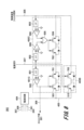
- FIG. 1 is a system configuration diagram showing an example of power redundancy in a conventional power supply system.
- the power supply system 100 shown in FIG. 1 has a configuration in which ECUs 103 to 106 are connected in a ring type in a zone architecture, and is an example of redundant power supply and communication without using power superimposition technology.
- Power supplies 101 and 102 serve as redundant power supplies, and power is supplied from power supply 102 to ECUs 103 to 106 only when power supply 101 fails.
- the power supply 102 supplies power to the ECU 104 via the power harness 111 and to the ECU 106 via the power harness 112. Further, the power supply 102 supplies power from the ECU 104 to the ECU 103 via the power harness 113, and from the ECU 106 to the ECU 105 via the power harness 114.
- the ECUs 103 to 106 are interconnected by redundant communication lines, and communication is also made redundant.
- ECU 103 and ECU 104 communicate via communication line 116 and communication line 120.
- ECU 103 and ECU 105 communicate via communication line 115 and communication line 119.
- ECU 104 and ECU 106 communicate via communication line 118 and communication line 122.
- ECU 105 and ECU 106 communicate via communication line 117 and communication line 121.
- the ECU 104 supplies power to the sensor 133 via a power line 145, and controls and sends and receives data to and from the sensor 133 via a communication line 146. Further, the ECU 104 supplies power to the actuator 134 via a power line 147, and performs control and transfers data to and from the actuator 134 via a communication line 148.
- the ECU 105 supplies power to the sensor 135 via a power line 149, and controls and sends and receives data to and from the sensor 135 via a communication line 150. Further, the ECU 105 supplies power to the actuator 136 via a power line 151 and performs control and transfers data to and from the actuator 136 via a communication line 152.
- the ECU 106 supplies power to the sensor 137 via a power line 153, and performs control and sends/receives data to/from the sensor 137 via a communication line 154. Further, the ECU 106 supplies power to the actuator 138 via a power line 155 and performs control and transfers data to and from the actuator 138 via a communication line 156.
- the present invention makes it possible to provide power redundancy without increasing the number of power supply harnesses by, for example, providing power redundancy to an ECU used in a zone architecture through communication lines using power supply superimposition technology.
- the communication line connects all ECUs, so each power supply has jurisdiction over some ECUs and connects the power harness, and in the event of a failure, the communication line is used to supply power from a power supply that is not directly connected to the ECU through the power harness. It is done using When each power supply fails, it switches to power supply from the communication line, but since the power supply changes depending on the power supply that fails, a power supply switch that can supply power in both directions is used to provide redundant power supply using the communication line. conduct.
- FIG. 2 is a system configuration diagram showing an example of power redundancy in the power supply system according to the first embodiment.
- the power supply system 200 shown in FIG. 2 is an example in which power supply redundancy is achieved through communication lines using power superimposition technology, and the number of power supply harnesses is reduced.
- a ring-type network architecture is used for the power supply system 200.
- the power supply harnesses 109, 113 corresponding to the ECU 203 and the ECU 204, and the power supply harnesses 110, 114 corresponding to the ECU 205 and the ECU 206 are removed from the power supply system 100 of FIG. Instead, power superimposition for transmitting power and communication is performed in the communication line 216 connecting the ECU 203 and the ECU 204 and the communication line 217 connecting the ECU 205 and the ECU 206, thereby achieving power redundancy.
- the power supply system 200 includes a power supply 201, a power supply 202, an ECU 203, an ECU 204, an ECU 205, an ECU 206, power harnesses 207 to 208, power harnesses 211 to 212, communication lines 215 to 218 indicated by solid lines, and communication lines indicated by broken lines. It consists of 219 to 222. Communication lines 215 to 218 shown by solid lines are communication lines for power superimposition. Furthermore, communication lines 219 to 222 indicated by broken lines are communication lines for communication. However, the same communication lines for power superimposition as the communication lines 215 to 218 may be used for the communication lines 219 to 222.
- the ECU 205 and the ECU 206 can supply power to each other via the communication line 217 by superimposing power supplies. If power supply 201 fails, power from power supply 202 is supplied from ECU 206 to ECU 205 via communication line 217. Conversely, when power supply 202 fails, power from power supply 201 is supplied from ECU 205 to ECU 206 via communication line 217.
- the ECU 203 performs redundant communication with the ECU 204 via the communication line 216 and the communication line 220, performs redundant communication with the ECU 205 via the communication line 215 and the communication line 219, and sends and receives data. Further, the ECU 203 supplies power to the sensor 231 via a power line 241, and performs control and transfers data via a communication line 242. Further, the ECU 203 supplies power to the actuator 232 via a power line 243, and performs control and transfers data via a communication line 244.
- the number of sensors and actuators is not limited to one. Even if the number of sensors and actuators increases or decreases, the power supply redundancy configuration of the power supply system 200 remains the same.
- the power switch 302 receives the power from the power source 201 supplied via the power harness 207 and the power from the power source 202 supplied via the power line 305.
- the power switch 302 internally monitors the voltage passing through the power harness 207 and the voltage passing through the power line 305, determines which voltage should be connected to the output, and switches. Thereby, the power switch 302 connects to the ECU core unit 301 via the power line 307, to the transceiver 303 via the power line 306, to the sensor 231 via the power line 241, and to the actuator 232 via the power line 243. supply power to each.
- the first control circuit other ECUs that the first power supply is abnormal.
- other ECUs mounted on the vehicle can perform appropriate control such as operation continuation control in response to the fact that the first power supply is abnormal.
- the ECU core section 301 may include memory (ROM, RAM) and nonvolatile storage in addition to a processor (not shown).
- a processor such as a CPU (Central Processing Unit) or an MPU (Micro-Processing Unit) can be used as the processor of the ECU core section 301.
- the functions of the ECU core section in the embodiment of the present invention are realized by the processor executing a computer program stored in the ROM or nonvolatile storage.
- the comparator 502 compares the voltage from the power harness 207 with the threshold voltage of the threshold voltage source 503, and if the voltage from the power harness 207 is equal to or higher than the threshold voltage, the comparator 502 sets the output to Low level, turns on the MOSFET 501, and connects the power harness 207 and The power supply line 405 is electrically connected. On the other hand, if the voltage from the power harness 207 is lower than the threshold voltage, the comparator 502 sets the output to High level, turns off the MOSFET 501, and cuts off the connection between the power harness 207 and the power line 405. The output of comparator 502 is transmitted to ECU core section 301 via communication line 309.
- the voltage of the power supply line 405 starts in a low state, so MOSFET 501 and MOSFET 510 are turned off.
- the initial state is when the power is turned on, when the ECU 203 is started, when the car is started, etc.
- MOSFET 501 a diode is connected between the drain and the source, so if the voltage of the power harness 207 becomes higher than the threshold voltage of the diode, the power line 405 and the power harness 207 are electrically connected, and the voltage of the power line 405 is reduced. Since the value increases, MOSFET 501 is also turned on.
- the power supply switching device having the above configuration, in the event of a power supply failure, it is possible to switch between the power supply passing through the power supply harness and the power supply passing through the communication line at high speed and with low loss.
- FIG. 6 is a circuit diagram showing a second example of the own power switch 401A, other load switch 402A, and other power switch 403 that constitute the power supply switch 302.
- the configuration of the power switch 302 shown in FIG. 6 differs from the power switch 302 of the first example shown in FIG. 5 in that a level shifter (denoted as "LV" in the figure) is used instead of a threshold voltage source. point, and its operation is almost the same as the first example.
- a level shifter denoted as "LV" in the figure
- the self-power switch 401A is composed of a MOSFET 501, a comparator 502, and a level shifter 601.
- Level shifter 601 shifts the voltage from power supply harness 207 by a preset voltage and outputs it to comparator 502 .
- the comparator 502 outputs a Low level if the output voltage of the level shifter 601 is positive, and outputs a High level if the output voltage is negative, thereby controlling ON/OFF of the MOSFET 501.
- the output of the comparator 502 is transmitted to the ECU core section 301 via the communication line 309.
- the other load switch 402A is composed of a MOSFET 504, an OR circuit 505, a comparator 506, a level shifter 602, a comparator 508, and a level shifter 603.
- Level shifter 602 shifts the voltage from power supply harness 207 by a preset voltage and outputs the shifted voltage to comparator 506 .
- the comparator 506 outputs a Low level if the output voltage of the level shifter 602 is positive, and outputs a High level if the output voltage is negative.
- Level shifter 603 shifts the voltage from power supply line 305 by a preset voltage and outputs it to comparator 508 .
- the comparator 508 outputs a Low level if the output voltage of the level shifter 603 is positive, and outputs a High level if the output voltage is negative.
- the OR circuit 505 sets the output to High level if either the output voltage of the comparator 506 or the comparator 508 is High level, and sets the output to Low level if both output voltages are Low level, and turns ON/OFF of MOSFET 504. Control.
- a P-type MOSFET 701 with the drain-source direction opposite to that of the MOSFET 501 is added to the self-power switch 401B.
- the drain of MOSFET 501 and the drain of MOSFET 701 are connected, and the gate of MOSFET 701 is connected to the output terminal of comparator 502.
- MOSFET 702 with the drain-source direction opposite to that of the MOSFET 504 is added to the other load switch 402B.
- the drain of MOSFET 504 and the drain of MOSFET 702 are connected, and the gate of MOSFET 702 is connected to the output terminal of OR circuit 505.
- the source of MOSFET 701 of self-power switch 401B and the source of MOSFET 702 of other load switch 402B are connected. Further, each source of MOSFET 701 and MOSFET 702 is connected to power supply harness 207.
- MOSFET 703 whose drain-source direction is opposite to that of the MOSFET 510 is added to the other power switch 403B.
- the drain of MOSFET 510 and the drain of MOSFET 703 are connected, the source of MOSFET 703 is connected to power line 305, and the gate of MOSFET 703 is connected to power harness 207.
- MOSFET 701, MOSFET 702, and MOSFET 703 have diodes opposite to those of the original MOSFET 501, MOSFET 504, and MOSFET 510.
- the diodes of these MOSFETs 701 to 703 can prevent current leakage.
- the first switch circuit (self-power switch 401B) has a voltage drop of the first voltage (voltage of the power supply 201) that is lower than the threshold value.
- the first switching element MOSFET 501 that conducts current between the first power supply (power supply 201) and the first control circuit (ECU core section 301), and the In between, a switching element (MOSFET 701) connected in series with the first switching element and with opposite polarity is provided.
- the second switch circuit (other load switch 402B) connects the first power supply and the communication line (communication A second switching element (MOSFET 504) that conducts current between line 216 (power line 305) and a second switching element connected in series and with opposite polarity between the first power source and the communication line.
- element MOSFET 702
- the power switch circuit (other power switch 403B) energizes between the first control circuit and the communication line (communication line 216 (power line 305)) when the voltage drop of the first voltage is smaller than the threshold value. and a switching element (MOSFET 703) connected in series with the third switching element and with opposite polarity between the first control circuit and the communication line.
- FIG. 8 is a circuit diagram showing a fourth example of the own power switch 401C, other load switch 402C, and other power switch 403B that constitute the power supply switch 302.
- the configuration of the power switch 302 shown in FIG. 8 is different from the power switch 302 of the second example shown in FIG.
- Each switch has measures in place to prevent this from happening. That is, in the fourth example of the power supply switch 302, the same measures as in the third example are taken.
- a MOSFET 701 with the drain-source direction reversed to that of the MOSFET 501 is added between the drain of the MOSFET 501 and the power harness 207, and the gate of the MOSFET 701 is connected to the output terminal of the comparator 502.
- a MOSFET 702 with the drain-source direction reversed to that of the MOSFET 504 is added between the drain of the MOSFET 504 and the power supply harness 207, and the gate of the MOSFET 702 is connected to the output terminal of the OR circuit 505.
- MOSFET 701, MOSFET 702, and MOSFET 703 have diodes in opposite directions to the original MOSFET 501, MOSFET 504, and MOSFET 510.
- the diodes of these MOSFETs 701 to 703 can prevent current leakage.
- each switch of the power supply switch 302 may be configured by using an N-type MOSFET as the MOSFET of each switch described above. Further, other switching elements may be used instead of MOSFETs.
- self-power switch 401 when the self-power switches 401 to 401C are not distinguished or are collectively referred to, they may be simply referred to as "self-power switch 401.”
- the other load switches 402 to 402C may be referred to as “other load switches 402”
- the other power switches 403 and 403B may be referred to as “other power switches 403".
- the power supply voltage is supplied to the first control circuit (ECU core section 301) and the first control circuit.
- a first power source power source 201 that outputs a first voltage
- a first power source power harness 207 that is connected to the first control circuit and outputs the first voltage to the first control circuit. It is connected to a first switch circuit that cuts off the power supply (self-power switches 401 to 401C) and a communication line (for example, communication line 216) used for communication between the first power supply and the second control circuit.
- a second switch circuit (other load switches 402 to 402C) that cuts off the supply of the first voltage to the communication line, and a second switch circuit that outputs the second voltage that is supplied as the power supply voltage to the second control circuit.
- the second voltage is A power switch circuit (other power switches 403, 403B) that supplies power to the first control circuit via a communication line.
- power supply of the first voltage to the second control circuit and power supply of the second voltage to the first control circuit are two-way power transmission using a communication line.
- the first switch circuit cuts off the supply of the first voltage to the first control circuit when the voltage drop of the first voltage is equal to or higher than the threshold, and the second switch circuit cuts off the supply of the first voltage to the first control circuit. If the voltage drop in the voltage of switch to the second power source.
- the power supply source can be switched from the first power supply to the second power supply by bidirectional power transmission using power supply redundancy technology, so that the power supply harness can be changed from the conventional power supply harness.
- Power supply redundancy can be achieved without increasing the number of units.
- the first switch circuit (self-power switches 401 to 401C) is activated when the voltage drop of the first voltage is smaller than the threshold value.
- the first voltage is supplied to the first control circuit
- the second switch circuit (other load switches 402 to 402C) is configured such that the voltage drop of the first voltage is smaller than the threshold value and the voltage of the second voltage is lower than the threshold value. If the drop is equal to or greater than the threshold, the first voltage is supplied to the communication line, and the power switch circuit (other power switches 403, 403B) cuts off the first control circuit and the communication line.
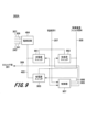
- FIG. 9 is a block diagram illustrating a configuration example of a power switch 302A included in the ECU 203.
- the configuration of the power supply switch 302A shown in FIG. 9 is different from the power supply switch 302 shown in FIG. The point is that the comparators, OR circuits, etc. in FIGS. 5 to 8 are combined into one controller 907.
- the power supply switch 302A includes a self-power switch 901, another load switch 902, another power switch 903, a controller 907, and a power supply circuit 404.
- the own power switch 901, other load switch 902, and other power switch 903 are all configured using one MOSFET or two MOSFETs as shown in FIGS. 5 to 8.
- the own power switch 901, the other load switch 902, and the other power switch 903 have the same switching function as the own power switch 401, the other load switch 402, and the other power switch 403 shown in FIG.
- the voltage from the power harness 207 and the voltage from the power line 305 are input to the controller 907. Then, the controller 907 controls the own power switch 901 via the communication line 309 and the other load switch 902 via the control line 905 according to the voltage of the power harness 207 and the voltage of the power line 305, The other power switch 903 is controlled via a control line 906.
- FIG. 10 is a circuit diagram showing a first example of the controller 907 that constitutes the power switch 302A.
- the controller 907 includes a comparator 1001, a threshold voltage source 1002, a comparator 1003, a threshold voltage source 1004, an OR circuit 1005, and a NOT circuit 1006.
- the comparator 1001 compares the voltage from the power harness 207 with the threshold voltage of the threshold voltage source 1002, and sets the output to Low level if the voltage from the power harness 207 is equal to or higher than the threshold voltage. If the voltage is lower than the threshold voltage, the output is set to High level. Comparator 1001 outputs a signal to communication line 309 according to the comparison result.
- Comparator 1003 compares the voltage from power line 305 with the threshold voltage of threshold voltage source 1004, and sets the output to Low level if the voltage from power line 305 is equal to or higher than the threshold voltage. If the voltage is lower than the threshold voltage, the output is set to High level.
- the OR circuit 1005 outputs a high level if either the output voltage of the comparator 1001 or the output voltage of the comparator 1003 is at a high level, and outputs a low level if both output voltages are at a low level.
- the OR circuit 1005 outputs a signal according to the logical operation result to the control line 905 connected to the other load switch 902.
- NOT circuit 1006 inverts the output value of comparator 1001 and outputs it to control line 906 connected to other power switch 903.
- NOT circuit 1006 outputs High level when the output voltage of comparator 1001 is Low level, and outputs Low level when the output voltage of comparator 1001 is High level.
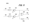
- controller 907 that constitutes the power switch 302A in this embodiment will be described with reference to FIG. 11.
- FIG. 11 is a circuit diagram showing a second example of the controller 907 that constitutes the power switch 302A.
- the configuration of the controller 907A shown in FIG. 11 differs from the controller 907 of the first example shown in FIG. 10 in that a level shifter (denoted as "LV" in the figure) is used instead of a threshold voltage source. Yes, and the operation is almost the same as the first example.
- a level shifter denoted as "LV" in the figure
- the controller 907A is composed of a comparator 1001, a level shifter 1101, a comparator 1003, a level shifter 1102, an OR circuit 1005, and a NOT circuit 1006.
- the level shifter 1101 shifts the voltage from the power supply harness 207 by a preset voltage and outputs it to the comparator 1001.
- the comparator 1001 outputs a low level when the output voltage of the level shifter 1101 is positive, and outputs a high level when the output voltage is negative.
- the level shifter 1102 shifts the voltage from the power supply line 305 by a preset voltage and outputs it to the comparator 1003.
- the comparator 1003 outputs a low level when the output voltage of the level shifter 1102 is positive, and outputs a high level when the output voltage is negative.
- the OR circuit 1005 outputs a high level if either of the output voltages of the comparator 1001 or the comparator 1003 is a high level, and outputs a low level if either output voltage is a low level.
- NOT circuit 1006 inverts the output value of comparator 1001. The NOT circuit 1006 outputs a high level when receiving a low level input, and outputs a low level when receiving a high level input.
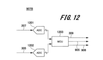
- FIG. 12 is a circuit diagram showing a third example of the controller 907 that constitutes the power switch 302A.
- the controller 907B shown in FIG. 12 includes an ADC (analog-digital converter) 1201, an ADC 1202, and a microprocessor (denoted as "MCU" in the figure) 1203.
- ADC analog-digital converter
- ADC analog-digital converter
- MCU Microcontrol Unit
- an MCU Micro Controller Unit
- an MCU Micro Controller Unit
- an MCU includes a processor, memory such as ROM or RAM, I/O, and the like. Since the controller 907B in this embodiment can convert the voltage (analog signal) from the power harness 207 and the power line 305 into digital data, the control content can be modified by programming.
- the ADC 1201 converts the voltage value from the power supply harness 207 into a digital value, and outputs the digital value to the microprocessor 1203. Further, the ADC 1202 converts the voltage value from the power supply line 305 into a digital value, and outputs the digital value to the microprocessor 1203.
- the output of the ADC 1201 and the output of the ADC 1202 are input to the microprocessor 1203. Then, if the output code (digital value of voltage) of the ADC 1201 is larger than the set code, the microprocessor 1203 sets the output to the communication line 309 to Low level, and the control line 903 connected to the other power switch 903 Set the output to High level. Furthermore, under other conditions, the microprocessor 1203 sets the output to the communication line 309 to High level and sets the output to the control line 906 to Low level.
- the microprocessor 1203 sets the output to the control line 905 connected to the other load switch 902 to High level, and Under other conditions, the output to the control line 905 is set to Low level.
- the determination control circuit (The comparators, OR circuits, etc. in FIGS. 5 to 8) are combined into one controller (controllers 907 to 907B). Therefore, in the power supply system according to this embodiment, the configuration of each switch circuit that constitutes the power switch can be simplified.
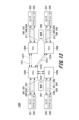
- FIG. 13 is a system configuration diagram showing an example of power redundancy in the power supply system according to the third embodiment.
- the power supply system 200 (FIG. 2) according to the first and second embodiments had a ring-type architecture using four ECUs 203 to 206, but the power supply system 1300 according to this embodiment has four ECUs.
- This is a star architecture using ECUs 1303 to 1306. Although an example with four ECUs is shown here, the basic connection method remains the same even if the number of ECUs increases.
- a central ECU (ECU 1303) and other ECUs (ECUs 1304 to 1306) are connected via communication lines.
- the star architecture has the advantage of reducing communication lines.
- the ECU 1303 and the ECU 1304 can supply power to each other via a communication line 1311 by superimposing power supplies. If power supply 201 fails, power from power supply 202 is supplied from ECU 1304 to ECU 1303 via communication line 1311. Conversely, when power supply 202 fails, power from power supply 201 is supplied from ECU 1303 to ECU 1304 via communication line 1311.
- the ECU 1303 and the ECU 1306, and the ECU 1303 and the ECU 1306 can supply power to each other via the communication line 1313 by superimposing power supplies. If power supply 201 fails, power from power supply 202 is supplied from ECU 1306 to ECU 1303 via communication line 1313. Conversely, when power supply 202 fails, power from power supply 201 is supplied from ECU 1303 to ECU 1306 via communication line 1313. Regarding power transmission between the ECU 1303 and the ECU 1305, the ECU 1303 and the ECU 1305 can supply power to each other via a communication line 1312 by superimposing power supplies. If power supply 201 fails, power from power supply 202 is supplied from ECU 1303 to ECU 1305 via communication line 1312.
- ECU 1303 performs redundant communication with ECU 1304 via communication line 1311 and communication line 1314, performs redundant communication with ECU 1305 via communication line 1312 and communication line 1315, and performs redundant communication with ECU 1305 via communication line 1313 and communication line 1316. It performs redundant communication with the ECU 1306 via the ECU 1306 to exchange data. Further, the ECU 1303 supplies power to the sensor 231 via a power line 241, and performs control and transfers data via a communication line 242. Further, the ECU 1303 supplies power to the actuator 232 via a power line 243, and performs control and transfers data via a communication line 244.
- the ECU 1304 performs redundant communication with the ECU 1303 via a communication line 1311 and a communication line 1314 to exchange data. Further, the ECU 1304 supplies power to the sensor 233 via a power line 245 and performs control and transfers data via a communication line 246. Further, the ECU 1304 supplies power to the actuator 234 via a power line 247 and performs control and transfers data via a communication line 248.
- the ECU 1305 performs redundant communication with the ECU 1303 via a communication line 1312 and a communication line 1315 to exchange data. Further, the ECU 1305 supplies power to the sensor 235 via a power line 249, and performs control and transfers data via a communication line 250. Further, the ECU 1305 supplies power to the actuator 236 via a power line 251, and performs control and transfers data via a communication line 252.
- the ECU 1306 performs redundant communication with the ECU 1303 via a communication line 1313 and a communication line 1316 to exchange data. Further, the ECU 1306 supplies power to the sensor 237 via a power line 253 and performs control and transfers data via a communication line 254. Further, the ECU 1306 supplies power to the actuator 238 via a power line 255 and performs control and transfers data via a communication line 256.
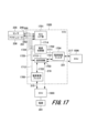
- the power superimposition filter 1404 is connected to the ECU 1304 via a communication line 1311, and exchanges communication signals or communication signals on which power is superimposed. Further, the power superimposing filter 1404 is connected to the power switch 1402 via a power line 1411 and to the transceiver 1403 via a communication line 1421. Further, the power superimposing filter 1404 is connected to a power superimposing filter 1405 and a power superimposing filter 1406 via a power line 1411. In the power superimposition filter 1404, only DC power and power having a frequency near DC pass between the communication line 1311 and the power line 1411, and only high-frequency communication signals pass between the communication line 1311 and the communication line 1421.
- the power switch 1402 receives the power from the power source 201 supplied via the power harness 207 and the power from the power source 202 supplied via the power line 1411.
- the power switch 1402 internally monitors the voltage passing through the power harness 207 and the voltage passing through the power line 1411, determines which voltage should be connected to the output, and switches. Thereby, the power switch 1402 connects to the ECU core unit 1401 via the power line 1413, to the transceiver 1403 via the power line 1412, to the sensor 231 via the power line 241, and to the actuator 232 via the power line 243. supply power to each.
- the power supply switch 1402 supplies power from the power supply harness 207 to the ECU core section 1401, the transceiver 1403, the sensor 231, and the actuator 232.
- the power source switch 1402 transfers the power transmitted through the power line 1411 to the ECU core section 1401, transceiver 1403, sensor 231, and actuator 232.
- the power supply switch 1402 can obtain power failure information about the power supply 201, it can also send the power failure information to the ECU core unit 1401 via the communication line 1424 and share the power failure information with other ECUs. can.
- the ECU core section 1401 controls a transceiver 1403 through a communication line 1425, and exchanges data with the ECU 1304, ECU 1305, and ECU 1306 (FIG. 13) via the transceiver 1403. Further, the ECU core unit 1401 controls the sensor 231 and the actuator 232, sends and receives data, and processes the data.
- the ECU 1503 and the ECU 1504 can supply power to each other via the communication line 216 by superimposing power supplies. If power supply 201 fails, power from power supply 202 is supplied from ECU 1504 to ECU 1503 via communication line 216. Conversely, when power supply 202 fails, power from power supply 201 is supplied from ECU 1503 to ECU 1504 via communication line 216.
- the ECU 1505 and the ECU 1506 can supply power to each other via a communication line 217 by superimposing power supplies. If power supply 201 fails, power from power supply 202 is supplied to ECU 1505 via communication line 217 via ECU 1504 and ECU 1506. Conversely, when power supply 202 fails, power from power supply 201 is supplied to ECU 1506 via communication line 217 via ECU 1503 and ECU 1505.
- ECU 1504 performs redundant communication with ECU 1503 via communication line 216 and communication line 220, performs redundant communication with ECU 1506 via communication line 218 and communication line 222, and exchanges data. Further, the ECU 1504 supplies power to the sensor 233 via a power line 245, and performs control and transfers data via a communication line 246. Further, the ECU 1504 supplies power to the actuator 234 via a power line 247, and performs control and transfers data via a communication line 248.
- ECU 1505 performs redundant communication with ECU 1503 via communication line 215 and communication line 219, performs redundant communication with ECU 1506 via communication line 217 and communication line 221, and sends and receives data. Further, the ECU 1505 supplies power to the sensor 235 via a power line 249, and performs control and transfers data via a communication line 250. Further, the ECU 1505 supplies power to the actuator 236 via a power line 251, and performs control and transfers data via a communication line 252.
- the ECU 1503 includes an ECU core section 1601, a power switch 1602, a transceiver 1603, a power superimposition filter 1604, and a power superimposition filter 1605.
- the basic functions of each processing block are the same as those of the ECU core section 301, power switch 302, transceiver 303, and power superimposition filter 304 shown in FIG.
- the power switch 1602 receives the power from the power source 201 supplied via the power harness 207 and the power from the power source 202 supplied via the power line 1611.
- the power supply switch 1602 internally monitors the voltage passing through the power supply harness 207 and the voltage passing through the power supply line 1611, determines which voltage should be connected to the output, and switches the voltage. Thereby, the power switch 1602 connects to the ECU core section 1601 via the power line 1613, to the transceiver 1603 via the power line 1612, to the sensor 231 via the power line 241, and to the actuator 232 via the power line 243. supply power to each.
- the ECU 1505 includes an ECU core section 1701, a power switch 1702, a transceiver 1703, a power superimposition filter 1704, and a power superimposition filter 1705.
- the basic functions of each processing block are the same as those of the ECU core section 301, power switch 302, transceiver 303, and power superimposition filter 304 shown in FIG.
- ECU 1505 has a slightly different wiring connection from ECU 1503 in that it does not have a power harness connected to it.
- the power superimposition filter 1704 is connected to the ECU 1506 via a communication line 217, and exchanges communication signals or communication signals on which power is superimposed. Further, the power superimposing filter 1704 is connected to a power switch 1702 via a power line 1711 and to a transmitter/receiver 1703 via a communication line 1721. In the power superimposition filter 1704, only DC power and power having a frequency near DC pass between the communication line 217 and the power line 1711, and only high-frequency communication signals pass between the communication line 217 and the communication line 1721.
- the power superimposition filter 1705 is connected to the ECU 1503 via a communication line 215, and exchanges communication signals or communication signals on which power is superimposed. Further, the power superimposing filter 1705 is connected to the power switch 1702 via a power line 1712 and to the transceiver 1703 via a communication line 1722. In the power superimposition filter 1705, only DC power and power having a frequency near DC pass between the communication line 215 and the power line 1712, and only high-frequency communication signals pass between the communication line 215 and the communication line 1722.
- the power switch 1702 receives the power of the power source 201 supplied via the power line 1712 and the power of the power source 202 supplied via the power line 1711.
- the power supply switch 1702 internally monitors the voltage passing through the power line 1712 and the voltage passing through the power line 1711, determines which voltage should be connected to the output, and switches. Thereby, the power switch 1702 connects to the ECU core unit 1701 via the power line 1714, to the transceiver 1703 via the power line 1713, to the sensor 235 via the power line 249, and to the actuator 236 via the power line 251. supply power to each.
- the power supply switch 1702 supplies power from the power line 1712 to the ECU core section 1701, the transceiver 1703, the sensor 235, and the actuator 236.
- the power source switch 1702 transfers the power transmitted through the power line 1711 to the ECU core section 1701, transceiver 1703, sensor 235, and actuator 236.
- the power supply switch 1702 can obtain power failure information about the power supply 201, it can also send the power failure information to the ECU core unit 1701 via the communication line 1724 and share the power failure information with other ECUs. can.
- the transceiver 1703 communicates with the ECU 1506 via the communication line 217 that passes through the communication line 1721 and the power superimposing filter 1704, and the communication line 221. Further, the transceiver 1703 communicates with the ECU 1503 via a communication line 215 and a communication line 219 via a communication line 1722 and a power superimposing filter 1705. The transceiver 1703 then exchanges transmission signals and reception signals for other ECUs with the ECU core section 1701 via the communication line 1725.
- the ECU core section 1701 controls the transmitter/receiver 1703 through the communication line 1725, and exchanges data with the ECU 1503, ECU 1504, and ECU 1506 (FIG. 15) via the transmitter/receiver 1703. Further, the ECU core unit 1701 controls the sensor 235 and the actuator 236, sends and receives data, and processes the data.
- the present invention can also be applied to an architecture that includes an integrated ECU that can receive power supply from the power sources 201 and 202 and that controls multiple ECUs in an integrated manner.
- the present invention is not limited to the embodiments described above, and it goes without saying that various other applications and modifications can be made without departing from the gist of the present invention as set forth in the claims.
- the configurations thereof are explained in detail and specifically in order to explain the present invention in an easy-to-understand manner, and the embodiments are not necessarily limited to those having all the explained components.
- each of the above-mentioned configurations, functions, processing units, etc. may be partially or entirely realized in hardware by, for example, designing an integrated circuit.
- a broadly defined processor device such as an FPGA (Field Programmable Gate Array) or an ASIC (Application Specific Integrated Circuit) may be used.
- control lines and information lines are shown that are considered necessary for explanation, and not all control lines and information lines are necessarily shown in the product. In reality, almost all the components may be considered to be interconnected.
- 200 power supply system, 201,202...power supply, 203-206...ECU, 207,208,211,212...power harness, 301...ECU core section, 302...power supply switching section, 303...transmitter/receiver, 304...power superimposition Filter, 401...own power switch, 402...other load switch, 403...other power switch
Landscapes
- Engineering & Computer Science (AREA)
- Mechanical Engineering (AREA)
- Power Engineering (AREA)
- Business, Economics & Management (AREA)
- Emergency Management (AREA)
- Automation & Control Theory (AREA)
- Direct Current Feeding And Distribution (AREA)
Priority Applications (2)
| Application Number | Priority Date | Filing Date | Title |
|---|---|---|---|
| DE112023000521.4T DE112023000521T5 (de) | 2022-06-22 | 2023-06-07 | Leistungsversorgungssystem und elektronische Steuervorrichtung |
| US18/842,841 US20250178548A1 (en) | 2022-06-22 | 2023-06-07 | Power supply system and electronic control device |
Applications Claiming Priority (2)
| Application Number | Priority Date | Filing Date | Title |
|---|---|---|---|
| JP2022100467A JP7708715B2 (ja) | 2022-06-22 | 2022-06-22 | 電源供給システム及び電子制御装置 |
| JP2022-100467 | 2022-06-22 |
Publications (1)
| Publication Number | Publication Date |
|---|---|
| WO2023248794A1 true WO2023248794A1 (ja) | 2023-12-28 |
Family
ID=89379877
Family Applications (1)
| Application Number | Title | Priority Date | Filing Date |
|---|---|---|---|
| PCT/JP2023/021135 Ceased WO2023248794A1 (ja) | 2022-06-22 | 2023-06-07 | 電源供給システム及び電子制御装置 |
Country Status (4)
| Country | Link |
|---|---|
| US (1) | US20250178548A1 (https=) |
| JP (1) | JP7708715B2 (https=) |
| DE (1) | DE112023000521T5 (https=) |
| WO (1) | WO2023248794A1 (https=) |
Families Citing this family (1)
| Publication number | Priority date | Publication date | Assignee | Title |
|---|---|---|---|---|
| WO2025192007A1 (ja) * | 2024-03-12 | 2025-09-18 | Astemo株式会社 | アクチュエータ制御システム及びステアリング装置 |
Citations (6)
| Publication number | Priority date | Publication date | Assignee | Title |
|---|---|---|---|---|
| JP2004338577A (ja) * | 2003-05-16 | 2004-12-02 | Hitachi Ltd | 車両用電力供給装置及び電力供給方法 |
| WO2018008360A1 (ja) * | 2016-07-07 | 2018-01-11 | 株式会社オートネットワーク技術研究所 | リレー装置 |
| US20200136427A1 (en) * | 2018-10-31 | 2020-04-30 | Aptiv Technologies Limited | Electronic circuit for redundant supply of an electric load |
| WO2020137091A1 (ja) * | 2018-12-26 | 2020-07-02 | 日立オートモティブシステムズ株式会社 | 車載制御システム |
| JP2021125928A (ja) * | 2020-02-03 | 2021-08-30 | トヨタ自動車株式会社 | 車両用制御装置、方法、プログラム、及び車両 |
| WO2021220564A1 (ja) * | 2020-04-28 | 2021-11-04 | 日立Astemo株式会社 | 車載ネットワークシステムおよび電子制御装置 |
Family Cites Families (4)
| Publication number | Priority date | Publication date | Assignee | Title |
|---|---|---|---|---|
| JP4365647B2 (ja) * | 2003-09-05 | 2009-11-18 | 三菱電機株式会社 | 車載電子制御装置の電源回路 |
| JP5734472B1 (ja) * | 2014-01-29 | 2015-06-17 | 三菱電機株式会社 | 車載電子制御装置 |
| JP6900959B2 (ja) | 2018-02-21 | 2021-07-14 | 株式会社デンソーエレクトロニクス | ワイパ駆動回路 |
| CN115742783B (zh) * | 2021-09-03 | 2025-08-05 | 比亚迪股份有限公司 | 配电器、车辆的充配电系统、车辆以及充电桩 |
-
2022
- 2022-06-22 JP JP2022100467A patent/JP7708715B2/ja active Active
-
2023
- 2023-06-07 US US18/842,841 patent/US20250178548A1/en active Pending
- 2023-06-07 DE DE112023000521.4T patent/DE112023000521T5/de active Pending
- 2023-06-07 WO PCT/JP2023/021135 patent/WO2023248794A1/ja not_active Ceased
Patent Citations (6)
| Publication number | Priority date | Publication date | Assignee | Title |
|---|---|---|---|---|
| JP2004338577A (ja) * | 2003-05-16 | 2004-12-02 | Hitachi Ltd | 車両用電力供給装置及び電力供給方法 |
| WO2018008360A1 (ja) * | 2016-07-07 | 2018-01-11 | 株式会社オートネットワーク技術研究所 | リレー装置 |
| US20200136427A1 (en) * | 2018-10-31 | 2020-04-30 | Aptiv Technologies Limited | Electronic circuit for redundant supply of an electric load |
| WO2020137091A1 (ja) * | 2018-12-26 | 2020-07-02 | 日立オートモティブシステムズ株式会社 | 車載制御システム |
| JP2021125928A (ja) * | 2020-02-03 | 2021-08-30 | トヨタ自動車株式会社 | 車両用制御装置、方法、プログラム、及び車両 |
| WO2021220564A1 (ja) * | 2020-04-28 | 2021-11-04 | 日立Astemo株式会社 | 車載ネットワークシステムおよび電子制御装置 |
Also Published As
| Publication number | Publication date |
|---|---|
| DE112023000521T5 (de) | 2024-12-12 |
| US20250178548A1 (en) | 2025-06-05 |
| JP2024001663A (ja) | 2024-01-10 |
| JP7708715B2 (ja) | 2025-07-15 |
Similar Documents
| Publication | Publication Date | Title |
|---|---|---|
| WO2015129311A1 (ja) | モータ制御システムおよびモータ制御方法 | |
| JP2013015987A (ja) | ワイヤハーネス構造体及び電子制御ユニット | |
| WO2023248794A1 (ja) | 電源供給システム及び電子制御装置 | |
| KR101715331B1 (ko) | 복수의 통신 방식을 선택적으로 이용하는 차량용 통신 송수신기 | |
| US10250408B2 (en) | Communication device | |
| US6404326B1 (en) | Redundant power communications circuit | |
| US20040076429A1 (en) | Network component for an optical network comprising an emergency operation function, especially for an optical network in ring topology | |
| WO2021261014A1 (ja) | 信号伝送装置、信号伝送システム | |
| JP5416673B2 (ja) | 信号伝送回路、スイッチング素子駆動回路及び電力変換装置 | |
| EP1359057B1 (en) | Vehicle data transmission system with link redundancy | |
| US6934434B1 (en) | Circuit for switching optical paths | |
| US20030081632A1 (en) | Communications system, in particular for a motor vehicle | |
| US9461883B2 (en) | Coupling device for a data transmission network and data transmission network | |
| JP7535658B2 (ja) | 電子制御装置及び電子制御システム | |
| JP2006333007A (ja) | 車両通信システム及びデータ通信方法 | |
| JP2003244934A (ja) | 電力変換器バルブのための駆動装置 | |
| WO2015104978A1 (ja) | 車両用電気配線装置 | |
| JP2002123344A (ja) | 低電力トランシーバ | |
| CN112440908B (zh) | 网络系统 | |
| JP7568830B2 (ja) | I/oユニット、および通信システム | |
| US12572487B2 (en) | I/O unit, master unit, and communications system | |
| US11407313B2 (en) | Power supply circuit | |
| JP2007134906A (ja) | 監視制御装置 | |
| JPH02305145A (ja) | カレントループ伝送システム | |
| JP2023169933A (ja) | 制御装置、通信制御方法、通信制御プログラム |
Legal Events
| Date | Code | Title | Description |
|---|---|---|---|
| 121 | Ep: the epo has been informed by wipo that ep was designated in this application |
Ref document number: 23826981 Country of ref document: EP Kind code of ref document: A1 |
|
| WWE | Wipo information: entry into national phase |
Ref document number: 18842841 Country of ref document: US |
|
| WWE | Wipo information: entry into national phase |
Ref document number: 112023000521 Country of ref document: DE |
|
| WWP | Wipo information: published in national office |
Ref document number: 18842841 Country of ref document: US |
|
| 122 | Ep: pct application non-entry in european phase |
Ref document number: 23826981 Country of ref document: EP Kind code of ref document: A1 |