WO2023243619A1 - プリント配線板用基板及びプリント配線板 - Google Patents
プリント配線板用基板及びプリント配線板 Download PDFInfo
- Publication number
- WO2023243619A1 WO2023243619A1 PCT/JP2023/021821 JP2023021821W WO2023243619A1 WO 2023243619 A1 WO2023243619 A1 WO 2023243619A1 JP 2023021821 W JP2023021821 W JP 2023021821W WO 2023243619 A1 WO2023243619 A1 WO 2023243619A1
- Authority
- WO
- WIPO (PCT)
- Prior art keywords
- printed wiring
- wiring board
- conductive layer
- main surface
- board substrate
- Prior art date
- Legal status (The legal status is an assumption and is not a legal conclusion. Google has not performed a legal analysis and makes no representation as to the accuracy of the status listed.)
- Ceased
Links
Images


Classifications
-
- H—ELECTRICITY
- H05—ELECTRIC TECHNIQUES NOT OTHERWISE PROVIDED FOR
- H05K—PRINTED CIRCUITS; CASINGS OR CONSTRUCTIONAL DETAILS OF ELECTRIC APPARATUS; MANUFACTURE OF ASSEMBLAGES OF ELECTRICAL COMPONENTS
- H05K3/00—Apparatus or processes for manufacturing printed circuits
- H05K3/38—Improvement of the adhesion between the insulating substrate and the metal
-
- H—ELECTRICITY
- H05—ELECTRIC TECHNIQUES NOT OTHERWISE PROVIDED FOR
- H05K—PRINTED CIRCUITS; CASINGS OR CONSTRUCTIONAL DETAILS OF ELECTRIC APPARATUS; MANUFACTURE OF ASSEMBLAGES OF ELECTRICAL COMPONENTS
- H05K1/00—Printed circuits
- H05K1/02—Details
- H05K1/03—Use of materials for the substrate
-
- H—ELECTRICITY
- H05—ELECTRIC TECHNIQUES NOT OTHERWISE PROVIDED FOR
- H05K—PRINTED CIRCUITS; CASINGS OR CONSTRUCTIONAL DETAILS OF ELECTRIC APPARATUS; MANUFACTURE OF ASSEMBLAGES OF ELECTRICAL COMPONENTS
- H05K1/00—Printed circuits
- H05K1/02—Details
- H05K1/03—Use of materials for the substrate
- H05K1/0313—Organic insulating material
- H05K1/032—Organic insulating material consisting of one material
- H05K1/034—Organic insulating material consisting of one material containing halogen
-
- H—ELECTRICITY
- H05—ELECTRIC TECHNIQUES NOT OTHERWISE PROVIDED FOR
- H05K—PRINTED CIRCUITS; CASINGS OR CONSTRUCTIONAL DETAILS OF ELECTRIC APPARATUS; MANUFACTURE OF ASSEMBLAGES OF ELECTRICAL COMPONENTS
- H05K1/00—Printed circuits
- H05K1/02—Details
- H05K1/03—Use of materials for the substrate
- H05K1/0313—Organic insulating material
- H05K1/0353—Organic insulating material consisting of two or more materials, e.g. two or more polymers, polymer + filler, + reinforcement
- H05K1/0373—Organic insulating material consisting of two or more materials, e.g. two or more polymers, polymer + filler, + reinforcement containing additives, e.g. fillers
-
- H—ELECTRICITY
- H05—ELECTRIC TECHNIQUES NOT OTHERWISE PROVIDED FOR
- H05K—PRINTED CIRCUITS; CASINGS OR CONSTRUCTIONAL DETAILS OF ELECTRIC APPARATUS; MANUFACTURE OF ASSEMBLAGES OF ELECTRICAL COMPONENTS
- H05K1/00—Printed circuits
- H05K1/02—Details
- H05K1/09—Use of materials for the conductive, e.g. metallic pattern
- H05K1/092—Dispersed materials, e.g. conductive pastes or inks
- H05K1/097—Inks comprising nanoparticles and specially adapted for being sintered at low temperature
-
- H—ELECTRICITY
- H05—ELECTRIC TECHNIQUES NOT OTHERWISE PROVIDED FOR
- H05K—PRINTED CIRCUITS; CASINGS OR CONSTRUCTIONAL DETAILS OF ELECTRIC APPARATUS; MANUFACTURE OF ASSEMBLAGES OF ELECTRICAL COMPONENTS
- H05K3/00—Apparatus or processes for manufacturing printed circuits
- H05K3/10—Apparatus or processes for manufacturing printed circuits in which conductive material is applied to the insulating support in such a manner as to form the desired conductive pattern
- H05K3/108—Apparatus or processes for manufacturing printed circuits in which conductive material is applied to the insulating support in such a manner as to form the desired conductive pattern by semi-additive methods; masks therefor
-
- H—ELECTRICITY
- H05—ELECTRIC TECHNIQUES NOT OTHERWISE PROVIDED FOR
- H05K—PRINTED CIRCUITS; CASINGS OR CONSTRUCTIONAL DETAILS OF ELECTRIC APPARATUS; MANUFACTURE OF ASSEMBLAGES OF ELECTRICAL COMPONENTS
- H05K3/00—Apparatus or processes for manufacturing printed circuits
- H05K3/10—Apparatus or processes for manufacturing printed circuits in which conductive material is applied to the insulating support in such a manner as to form the desired conductive pattern
- H05K3/18—Apparatus or processes for manufacturing printed circuits in which conductive material is applied to the insulating support in such a manner as to form the desired conductive pattern using precipitation techniques to apply the conductive material
- H05K3/181—Apparatus or processes for manufacturing printed circuits in which conductive material is applied to the insulating support in such a manner as to form the desired conductive pattern using precipitation techniques to apply the conductive material by electroless plating
-
- H—ELECTRICITY
- H05—ELECTRIC TECHNIQUES NOT OTHERWISE PROVIDED FOR
- H05K—PRINTED CIRCUITS; CASINGS OR CONSTRUCTIONAL DETAILS OF ELECTRIC APPARATUS; MANUFACTURE OF ASSEMBLAGES OF ELECTRICAL COMPONENTS
- H05K3/00—Apparatus or processes for manufacturing printed circuits
- H05K3/22—Secondary treatment of printed circuits
- H05K3/24—Reinforcing of the conductive pattern
- H05K3/245—Reinforcing conductive patterns made by printing techniques or by other techniques for applying conductive pastes, inks or powders; Reinforcing other conductive patterns by such techniques
- H05K3/246—Reinforcing conductive paste, ink or powder patterns by other methods, e.g. by plating
-
- H—ELECTRICITY
- H05—ELECTRIC TECHNIQUES NOT OTHERWISE PROVIDED FOR
- H05K—PRINTED CIRCUITS; CASINGS OR CONSTRUCTIONAL DETAILS OF ELECTRIC APPARATUS; MANUFACTURE OF ASSEMBLAGES OF ELECTRICAL COMPONENTS
- H05K2201/00—Indexing scheme relating to printed circuits covered by H05K1/00
- H05K2201/01—Dielectrics
- H05K2201/0137—Materials
- H05K2201/015—Fluoropolymer, e.g. polytetrafluoroethylene [PTFE]
-
- H—ELECTRICITY
- H05—ELECTRIC TECHNIQUES NOT OTHERWISE PROVIDED FOR
- H05K—PRINTED CIRCUITS; CASINGS OR CONSTRUCTIONAL DETAILS OF ELECTRIC APPARATUS; MANUFACTURE OF ASSEMBLAGES OF ELECTRICAL COMPONENTS
- H05K2201/00—Indexing scheme relating to printed circuits covered by H05K1/00
- H05K2201/02—Fillers; Particles; Fibers; Reinforcement materials
- H05K2201/0203—Fillers and particles
- H05K2201/0206—Materials
- H05K2201/0209—Inorganic, non-metallic particles
-
- H—ELECTRICITY
- H05—ELECTRIC TECHNIQUES NOT OTHERWISE PROVIDED FOR
- H05K—PRINTED CIRCUITS; CASINGS OR CONSTRUCTIONAL DETAILS OF ELECTRIC APPARATUS; MANUFACTURE OF ASSEMBLAGES OF ELECTRICAL COMPONENTS
- H05K2201/00—Indexing scheme relating to printed circuits covered by H05K1/00
- H05K2201/03—Conductive materials
- H05K2201/0332—Structure of the conductor
- H05K2201/0335—Layered conductors or foils
- H05K2201/0344—Electroless sublayer, e.g. Ni, Co, Cd or Ag; Transferred electroless sublayer
Definitions
- the present disclosure relates to a printed wiring board substrate and a printed wiring board.
- This application claims priority based on Japanese Application No. 2022-097564 filed on June 16, 2022, and incorporates all the contents described in the said Japanese application.
- Patent Document 1 A composite film is described in JP-A-2006-69074 (Patent Document 1).
- the composite film described in Patent Document 1 includes a resin film and a metal layer.
- the resin film has a main surface.
- the resin film is made of, for example, fluororesin.
- the metal layer is arranged on the main surface of the resin film.
- the metal layer is formed by sputtering.
- the printed wiring board substrate of the present disclosure includes a base film having a main surface and a conductive layer disposed on the main surface.
- the base film is made of fluororesin.
- a conductive layer is a layer that includes a plurality of conductive particles that are bonded to each other.
- the amount of nitrogen present on the main surface is 0.2 atomic percent or more.
- FIG. 1 is a cross-sectional view of a printed wiring board substrate 100.
- FIG. 2 is a sectional view of a modified example of the printed wiring board substrate 100.
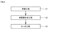
- FIG. 3 is a manufacturing process diagram of the printed wiring board substrate 100.
- FIG. 4 is a sectional view illustrating the preparation step S1.
- FIG. 5 is a cross-sectional view illustrating the conductive layer forming step S2.
- FIG. 6 is a cross-sectional view of printed wiring board 200.
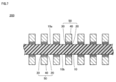
- FIG. 7 is a cross-sectional view of a modified example of printed wiring board 200.
- FIG. 8 is a manufacturing process diagram of the printed wiring board 200.
- FIG. 9 is a cross-sectional view illustrating the resist pattern forming step S4.
- FIG. 10 is a cross-sectional view illustrating the electrolytic plating step S5.
- FIG. 11 is a cross-sectional view illustrating the resist pattern removal step S6.
- FIG. 12 is a SEM image of a cross section of the printed
- the present disclosure has been made in view of the problems of the prior art as described above. More specifically, the present disclosure provides a printed wiring board substrate that can improve the adhesion of wiring.
- the printed wiring board substrate according to the embodiment includes a base film having a main surface and a conductive layer disposed on the main surface.
- the base film is made of fluororesin.
- a conductive layer is a layer that includes a plurality of conductive particles that are bonded to each other.
- the amount of nitrogen present on the main surface is 0.2 atomic percent or more.
- the conductive particles may be particles whose main component is copper or silver.
- the thickness of the conductive layer may be 0.05 ⁇ m or more and 2.0 ⁇ m or less.
- the average particle diameter of the conductive particles may be 1 nm or more and 500 nm or less.
- the printed wiring board substrates of (1) to (4) above may further include a copper plating layer disposed on the conductive layer.
- the copper plating layer may be an electroless copper plating layer or an electrolytic copper plating layer.
- the base film may be formed of a fluororesin containing a filler.
- the filler may be formed of silica.
- the fluororesin is polytetrafluoroethylene.
- the printed wiring board according to the embodiment includes a base film having a main surface and wiring arranged on the main surface.
- the base film is made of fluororesin.
- the wiring has a conductive layer disposed on the main surface.
- a conductive layer is a layer that includes a plurality of conductive particles that are bonded to each other.
- the amount of nitrogen present on the main surface is 0.2 atomic percent or more.
- the printed wiring board substrate according to the embodiment will be referred to as a printed wiring board substrate 100
- the printed wiring board according to the embodiment will be referred to as a printed wiring board 200.
- FIG. 1 is a cross-sectional view of a printed wiring board substrate 100.
- the printed wiring board substrate 100 has a base film 10, a conductive layer 20, and a copper plating layer 30, as shown in FIG.
- the base film 10 has a first main surface 10a and a second main surface 10b.
- the first main surface 10a and the second main surface 10b are end faces of the base film 10 in the thickness direction.
- the second main surface 10b is the opposite surface to the first main surface 10a.
- the base film 10 is made of fluororesin.
- the fluororesin is, for example, PTFE (polytetrafluoroethylene).
- PTFE polytetrafluoroethylene
- the fluororesin used for the base film 10 is not limited to this.
- the fluororesin used for the base film 10 may be PFA (tetrafluoroethylene/perfluoroalkyl vinyl ether copolymer) or FEP (tetrafluoroethylene/hexafluoropropylene copolymer).
- the base film 10 may be formed of a fluororesin containing filler.
- the filler may be silica. However, the filler may be made of other materials.
- the filler may be spherical.
- the filler may have an average particle size of 0.3 ⁇ m or more and 4.0 ⁇ m or less.
- the average particle size of the filler is measured by observing a cross section using a scanning electron microscope (SEM) and averaging the particle sizes of the filler observed in the cross section.
- the particle diameter of the filler may be calculated manually from the above-mentioned SEM image, or may be calculated using image processing.
- the area of the cross section is 20 ⁇ m ⁇ 20 ⁇ m.
- the method for preparing the sample for cross-sectional observation is not particularly limited, but in order to accurately measure the particle size, the sample is prepared using, for example, a Cross Section Polisher (registered trademark) manufactured by JEOL Ltd. .
- the volume ratio of the filler to the fluororesin may be 1.2 or more, or 1.5 or more.
- the filler and the conductive layer 20 may be in contact with each other, or there may be a distance between the filler and the conductive layer 20.
- a fluororesin may be present between the filler and the conductive layer 20. This distance may be 0.01 ⁇ m or more and 0.5 ⁇ m or less, or 0.05 ⁇ m or more and 0.3 ⁇ m or less.
- any cross section perpendicular to the first main surface 10a a line parallel to the first main surface 10a of the fluororesin layer within the above distance (0.01 ⁇ m or more and 0.5 ⁇ m or less) between the filler and the conductive layer 20
- the total length along the direction may be 5% or more, or 10% or more of the entire length of the first main surface 10a in the cross section. In this case, the above-described effect of improving adhesion is sufficiently ensured.
- the conductive layer 20 is arranged on the first main surface 10a.
- T be the thickness of the conductive layer 20.
- T may be 0.05 ⁇ m or more and 2.0 ⁇ m or less. If the thickness of the conductive layer 20 is less than 0.05 ⁇ m, the conductivity will be insufficient, and during the electrolytic plating step (S5) described below, defects may occur in the electrolytic plated layer or variations in the thickness distribution of the electrolytic plated layer may occur. becomes larger. If the thickness of the conductive layer 20 exceeds 2.0 ⁇ m, the amount of etching becomes too large in the etching step (S7) described below, and the variation in circuit width due to the variation in etching becomes large.
- the conductive layer 20 is a layer of multiple conductive particles that are bonded to each other.
- the thickness of the conductive layer 20 can be measured by the following method. The sample is embedded in resin and the machined surface is prefinished by mechanical polishing. This processed surface was cross-sectionally processed using an Ar ion beam (cross-section polisher) and coated with 2 nm of carbon. Measure the thickness of layer 20. The thickness is the average value of the measured values at 10 arbitrary points.
- the conductive layer 20 is a porous body.
- two adjacent conductive particles are bonded to each other.
- the conductive particles that are bonded to each other may be sintered. There may be a portion in the conductive layer 20 where two adjacent conductive particles are not bonded to each other.
- the plurality of conductive particles at the interface with the first main surface 10a are fixed to the first main surface 10a. However, some of the plurality of conductive particles at the interface with the first main surface 10a may not be fixed to the first main surface 10a.
- the conductive particles are made of a conductive material.
- the conductive particles are particles whose main component is, for example, copper (Cu).
- the conductive particles may be particles whose main component is silver (Ag).
- copper being the main component of the conductive particles means that the content of copper in the conductive particles is more than 50% by mass. The same applies when silver is used.
- the conductive layer 20 may contain a plurality of types of conductive particles made of different materials.
- the average particle diameter of the conductive particles is, for example, 1 nm or more and 500 nm or less. When the average particle size of the conductive particles is less than 1 nm, oxidation tends to proceed, resulting in a decrease in conductivity.
- the electrolytic plating step (S5) to be described later defects may occur in the electrolytic plating layer, and variations in the thickness distribution of the electrolytic plating layer may become large.
- the average particle size of the conductive particles exceeds 500 nm, it is difficult to obtain bonding between the particles by firing, resulting in a decrease in conductivity.
- defects may occur in the electrolytic plating layer, and variations in the thickness distribution of the electrolytic plating layer may become large.
- the average particle size of the conductive particles is measured by a particle size distribution device (for example, Microtrac particle size distribution meter UPA-150EX manufactured by Nikkiso Co., Ltd.).
- the amount of nitrogen present on the first main surface 10a is 0.2 atomic percent or more.
- the amount of nitrogen present on the first main surface 10a is measured by XPS (X-ray photoelectron spectroscopy) analysis. More specifically, the conductive layer 20 disposed on the first main surface 10a is removed using an acidic solution, and then an XPS analysis is performed on the first main surface 10a. Based on the peak area of the spectrum indicating the 1s orbit of nitrogen, the amount of nitrogen present per unit area on the first principal surface 10a is obtained.
- the copper plating layer 30 is arranged on the conductive layer 20.
- the copper plating layer 30 is a copper layer formed by plating.
- the copper plating layer 30 is, for example, an electroless copper plating layer, that is, a copper layer formed by electroless plating.
- the copper plating layer 30 may be an electrolytic copper plating layer, that is, a copper layer formed by electrolytic plating. Note that the printed wiring board substrate 100 does not need to have the copper plating layer 30.
- FIG. 2 is a sectional view of a modified example of the printed wiring board substrate 100.
- a conductive layer 20 may also be disposed on the second main surface 10b.
- the copper plating layer 30 may be arranged on the conductive layer 20 on the second main surface 10b.
- Method for manufacturing printed wiring board substrate 100 A method for manufacturing printed wiring board substrate 100 will be described below.
- FIG. 3 is a manufacturing process diagram of the printed wiring board substrate 100.
- the method for manufacturing printed wiring board substrate 100 includes a preparation step S1, a conductive layer forming step S2, and a plating step S3.
- the conductive layer forming step S2 is performed after the preparation step S1.
- the plating step S3 is performed after the conductive layer forming step S2. Note that if the printed wiring board substrate 100 does not have the copper plating layer 30, the plating step S3 is omitted.
- FIG. 4 is a cross-sectional view illustrating the preparation step S1.
- the base film 10 is prepared in the preparation step S1.
- the conductive layer 20 is not formed on the first main surface 10a.
- the base film 10 prepared in the preparation step S1 may be subjected to pretreatment (for example, alkali treatment, plasma treatment) on the first main surface 10a before being subjected to the conductive layer forming step S2. , does not have to be done.
- pretreatment for example, alkali treatment, plasma treatment
- FIG. 5 is a cross-sectional view illustrating the conductive layer forming step S2.
- the conductive layer 20 is formed on the first main surface 10a.
- first, ink in which a plurality of conductive particles are dispersed is applied onto the first main surface 10a.
- the surfaces of the conductive particles contained in the ink are coated with an organic material.
- the organic material contains nitrogen and hydrogen.
- heating and pressure are applied to the ink applied on the first main surface 10a.
- Heating and pressurization are performed under a vacuum environment. Heating and pressurization are performed using, for example, a vacuum press machine. By heating and pressurizing, the solvent in the ink evaporates and the organic material covering the surface of the conductive particles is decomposed, resulting in sintering between the conductive particles and the formation of the conductive particles on the first main surface 10a. Sticking occurs.
- the conductive layer 20 is formed on the first main surface 10a. Note that when pressurization is performed, a plate member made of a metal material such as aluminum is placed between the head of the vacuum press machine and the ink.
- a copper plating layer 30 is formed on the conductive layer 20.
- the copper plating layer 30 is formed, for example, by electroless plating.
- the copper plating layer 30 may be formed by electrolytic plating.
- ink in which conductive particles are dispersed is applied to the first main surface 10a in the conductive layer forming step S2.
- the base film 10 is placed on the applied ink, and then the ink is heated and pressurized. Note that when ink is applied to the surface of a plate member made of a metal material such as aluminum, it is less likely to be repelled compared to when the ink is applied to the surface of base film 10 made of fluororesin.
- FIG. 6 is a cross-sectional view of the printed wiring board 200.
- printed wiring board 200 includes base film 10 and wiring 50.
- the wiring 50 is arranged on the first main surface 10a.
- the wiring 50 includes a conductive layer 20, a copper plating layer 30, and an electrolytic copper plating layer 40.
- Electrolytic copper plating layer 40 is arranged on copper plating layer 30.
- the electrolytic copper plating layer 40 is a copper layer formed by electrolytic plating.
- Printed wiring board 200 does not need to have copper plating layer 30.
- FIG. 7 is a cross-sectional view of a modified example of printed wiring board 200.
- the wiring 50 may also be arranged on the second main surface 10b. Also in this case, printed wiring board 200 does not need to have copper plating layer 30.
- FIG. 8 is a manufacturing process diagram of the printed wiring board 200.
- the method for manufacturing printed wiring board 200 includes a resist pattern forming step S4, an electrolytic plating step S5, a resist pattern removing step S6, and an etching step S7.
- Printed wiring board 200 is formed using printed wiring board substrate 100.
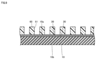
- FIG. 9 is a cross-sectional view illustrating the resist pattern forming step S4.
- a resist pattern 60 is formed on the conductive layer 20.
- the resist pattern 60 has an opening 61.
- the copper plating layer 30 is exposed through the opening 61.
- the resist pattern 60 is formed, for example, by exposing and developing a dry film resist to pattern it. Note that when printed wiring board 200 does not have copper plating layer 30, conductive layer 20 is exposed from opening 61.
- FIG. 10 is a cross-sectional view illustrating the electrolytic plating step S5.
- the electrolytic plating step S5 on the copper plating layer 30 exposed from the opening 61 (if the copper plating layer 30 is not provided, on the conductive layer 20 exposed from the opening 61)
- An electrolytic copper plating layer 40 is formed thereon.
- the electrolytic copper plating layer 40 is formed by applying electricity to the conductive layer 20 and the copper plating layer 30 and performing electrolytic plating on the copper plating layer 30 exposed through the opening 61.
- FIG. 11 is a cross-sectional view illustrating the resist pattern removal step S6. As shown in FIG. 11, in the resist pattern removal step S6, the resist pattern 60 is removed. In the etching step S7, the conductive layer 20 and the copper plating layer 30 between two adjacent electrolytic copper plating layers 40 are removed by wet etching. Through the above steps, printed wiring board 200 having the structure shown in FIG. 6 is formed.
- the organic material covering the surface of the conductive particles reacts with fluorine contained in the fluororesin of the base film 10, whereby a fluorine compound is generated.
- Ru Since the organic material covering the surface of the conductive particles contains hydrogen, this fluorine compound is hydrogen fluoride. Since hydrogen fluoride is a gas, the fluorine compound generated in the conductive layer forming step S2 is discharged to the outside through the conductive layer 20, which is a porous body, and is deposited at the interface between the conductive layer 20 and the first main surface 10a. There's nothing left. In other words, the conductive layer 20 is not corroded like water-soluble fluoride that is formed at the interface between the metal layer and the resin film when sputtering is performed.
- the conductive layer 20 that does not constitute the wiring 50 is removed by wet etching.
- the fluorine compound it is difficult for the fluorine compound to remain at the interface between the conductive layer 20 and the first main surface 10a, so the conductive layer 20 constituting the wiring 50 is difficult to be corroded when this wet etching is performed. . Therefore, according to the printed wiring board substrate 100, it is possible to suppress peeling of the wiring 50.
- the conductive layer forming step S2 nitrogen contained in the organic material coating the surface of the conductive particles at the interface with the first principal surface 10a is combined with carbon contained in the fluororesin of the base film 10.
- the conductive layer 20 is fixed to the first main surface 10a. Therefore, when the amount of nitrogen present on the first main surface 10a is measured by XPS analysis after removing the conductive layer 20 with an acidic solution, it is 0.2 atomic percent or more. Therefore, in the printed wiring board substrate 100 and the printed wiring board 200, the adhesion between the base film 10 and the conductive layer 20 is excellent.
- Quantera SXM manufactured by ULVAC PHI was used as an apparatus for XPS analysis, and the X-ray irradiation conditions were 100 ⁇ m ⁇ , 25 W, and 15 kV.
- the base film 10 is made of a fluororesin containing a filler, the base film 10 will be less likely to deform when pressure is applied in the conductive layer forming step S2, so the pressure will be more uniform with respect to the ink. join. Therefore, in this case, the conductive layer 20 can be formed more uniformly.
- the cost of the base film 10 can be reduced because silica is inexpensive.
- the average particle size of the filler is 0.3 ⁇ m or more and 4.0 ⁇ m or less, while suppressing the increase in unevenness of the first main surface 10a (second main surface 10b) due to pressurization in the conductive layer forming step S2, Deformation of the base film 10 during the pressurization can be suppressed.
- the volume ratio of the filler to the fluororesin is 1.2 or more, the conductive layer 20 can be formed more uniformly.
- FIG. 12 is a SEM image of a cross section of the printed wiring board substrate 100.
- FIG. 12 shows an SEM image of a cross section perpendicular to the first principal surface 10a.
- the cross section in FIG. 12 was processed using a Cross Section Polisher (registered trademark).
- the base film 10 is formed of PTFE containing a silica filler.
- FIG. 12 when there is a fluororesin between the filler and the conductive layer 20, there is a high temperature difference between the fluororesin and the conductive layer 20 when the pressure is applied in the conductive layer forming step S2. The pressure is applied, and the adhesion between the conductive layer 20 and the base film 10 is improved.
- the conductive layer 20 and the filler may come into contact with each other.
- the thickness of the fluororesin is more than 0.5 ⁇ m, the pressure increase effect described above becomes small. Therefore, when the thickness of the fluororesin is 0.01 ⁇ m or more and 0.5 ⁇ m or less, the adhesion between the conductive layer 20 and the base film 10 is particularly improved.
- the filler When the filler is spherical, it is easy to obtain a uniform distance between the filler and the conductive layer 20 along a part of the surface of the filler. Moreover, when the filler is spherical, the filler becomes difficult to break through the conductive layer 20 when pressurization is performed in the conductive layer forming step S2. In any cross section perpendicular to the first main surface 10a, the length of the fluororesin layer between the filler and the conductive layer 20 along the first main surface 10a is 5% or more of the width of the cross section. , the above-mentioned effect of improving adhesion is sufficiently ensured.
- the first main surface 10a of the fluororesin layer within the above distance (0.01 ⁇ m or more and 0.5 ⁇ m or less) between the filler and the conductive layer 20 in an arbitrary cross section perpendicular to the first main surface 10a.
- the total length along the parallel direction may be 5% or more, or 10% or more of the entire length of the first main surface 10a in the cross section. In this case, the above-mentioned effect of improving adhesion is sufficiently ensured.
- Samples 1 to 7 were prepared as examples, and sample 8 was prepared as a comparative example.
- the base film 10 was formed of PTFE containing filler.
- Sample 7 was formed from PTFE containing no filler.
- samples 1 to 4 and samples 6 to 7 copper particles with an average particle diameter of 70 nm were used as conductive particles.
- copper particles having an average particle size of 30 nm were used as conductive particles.
- samples 1 to 8 the pressure applied to the ink in the conductive layer forming step S2 was changed. In sample 8, this pressure is zero. That is, in sample 8, no pressure was applied to the ink during the conductive layer forming step S2.
- the maximum heating temperature (the maximum heating temperature of the hot plate of the press device) in the conductive layer forming step S2 was 350°C. Samples 1 to 8 were heated from room temperature to 350°C at a heating rate of 5°C/min, held at 350°C for 10 minutes, and then cooled to room temperature at a cooling rate of 5°C/min.
- Samples 1 to 5 Samples 7, and Samples 8, ink was applied to the first main surface 10a when the conductive layer forming step S2 was performed.
- sample 6 ink was applied to the surface of the aluminum plate member when the conductive layer forming step S2 was performed.
- samples 1 to 8 no pretreatment was performed on the first main surface 10a. Details of samples 1 to 8 are shown in Table 1.
- the amount of nitrogen present on the first main surface 10a and the adhesion of the conductive layer 20 to the first main surface 10a were measured.
- an electrolytic copper plating layer is formed on the conductive layer 20.
- the average value of the total thickness of the conductive layer 20 and the electrolytic copper plating layer is 20 ⁇ m.
- the base film 10 is fixed to a glass epoxy plate with double-sided tape, and the conductive layer 20 and the electrolytic copper plating layer are peeled off in a 180° direction with respect to the base film 10. It will be done.
- the measuring device used was Autograph AGS-X/500N manufactured by Shimadzu Corporation, the sample width was 5 mm, the peeling speed was 50 mm/min, and the measurement temperature was 25 ⁇ 3°C.
- the peel strength during this peeling is defined as the adhesion force of the conductive layer 20 to the first main surface 10a.
- the amount of nitrogen present was determined by etching and removing the copper layer using a copper etching solution containing 1 mol/L of copper chloride and 0.5 mol/L of hydrochloric acid, and then measuring the amount of nitrogen present in the base film by XPS analysis.
- ULVAC PHI's Quantera SXM was used as an apparatus, and the X-ray irradiation conditions were 100 ⁇ m ⁇ , 25 W, 15 kV). The results of these measurements are shown in Table 2.
- the amount of nitrogen present on the first main surface 10a was 0.2 atomic percent or more.
- the amount of nitrogen present on the first main surface 10a was less than 0.2 atomic percent. From this, it has become clear that by applying pressure in the conductive layer forming step S2, the amount of nitrogen present on the first main surface 10a becomes 0.2 atomic percent or more.
- the adhesion force of the conductive layer 20 to the first main surface 10a in Samples 1 to 7 was greater than the adhesion force of the conductive layer 20 in Sample 8 to the first main surface 10a. From this comparison, it has become clear that the adhesion of the conductive layer 20 and, by extension, the adhesion of the wiring 50 is improved when the amount of nitrogen present on the first principal surface 10a is 0.2 atomic percent or more. .
Landscapes
- Engineering & Computer Science (AREA)
- Microelectronics & Electronic Packaging (AREA)
- Manufacturing & Machinery (AREA)
- Chemical & Material Sciences (AREA)
- Nanotechnology (AREA)
- Dispersion Chemistry (AREA)
- Manufacturing Of Printed Wiring (AREA)
Priority Applications (3)
| Application Number | Priority Date | Filing Date | Title |
|---|---|---|---|
| US18/872,378 US20250365861A1 (en) | 2022-06-16 | 2023-06-13 | Substrate for printed circuit board and printed circuit board |
| JP2024528866A JPWO2023243619A1 (https=) | 2022-06-16 | 2023-06-13 | |
| CN202380046857.4A CN119302042A (zh) | 2022-06-16 | 2023-06-13 | 印刷布线板用基板及印刷布线板 |
Applications Claiming Priority (2)
| Application Number | Priority Date | Filing Date | Title |
|---|---|---|---|
| JP2022097564 | 2022-06-16 | ||
| JP2022-097564 | 2022-06-16 |
Publications (1)
| Publication Number | Publication Date |
|---|---|
| WO2023243619A1 true WO2023243619A1 (ja) | 2023-12-21 |
Family
ID=89191327
Family Applications (1)
| Application Number | Title | Priority Date | Filing Date |
|---|---|---|---|
| PCT/JP2023/021821 Ceased WO2023243619A1 (ja) | 2022-06-16 | 2023-06-13 | プリント配線板用基板及びプリント配線板 |
Country Status (4)
| Country | Link |
|---|---|
| US (1) | US20250365861A1 (https=) |
| JP (1) | JPWO2023243619A1 (https=) |
| CN (1) | CN119302042A (https=) |
| WO (1) | WO2023243619A1 (https=) |
Citations (2)
| Publication number | Priority date | Publication date | Assignee | Title |
|---|---|---|---|---|
| JP2016079346A (ja) * | 2014-10-21 | 2016-05-16 | 住友電工プリントサーキット株式会社 | 樹脂フィルム、プリント配線板用カバーレイ、プリント配線板用基板及びプリント配線板 |
| WO2019031071A1 (ja) * | 2017-08-08 | 2019-02-14 | 住友電気工業株式会社 | 高周波プリント配線板用基材 |
Family Cites Families (2)
| Publication number | Priority date | Publication date | Assignee | Title |
|---|---|---|---|---|
| US4849284A (en) * | 1987-02-17 | 1989-07-18 | Rogers Corporation | Electrical substrate material |
| US5055342A (en) * | 1990-02-16 | 1991-10-08 | International Business Machines Corporation | Fluorinated polymeric composition, fabrication thereof and use thereof |
-
2023
- 2023-06-13 CN CN202380046857.4A patent/CN119302042A/zh active Pending
- 2023-06-13 JP JP2024528866A patent/JPWO2023243619A1/ja active Pending
- 2023-06-13 WO PCT/JP2023/021821 patent/WO2023243619A1/ja not_active Ceased
- 2023-06-13 US US18/872,378 patent/US20250365861A1/en active Pending
Patent Citations (2)
| Publication number | Priority date | Publication date | Assignee | Title |
|---|---|---|---|---|
| JP2016079346A (ja) * | 2014-10-21 | 2016-05-16 | 住友電工プリントサーキット株式会社 | 樹脂フィルム、プリント配線板用カバーレイ、プリント配線板用基板及びプリント配線板 |
| WO2019031071A1 (ja) * | 2017-08-08 | 2019-02-14 | 住友電気工業株式会社 | 高周波プリント配線板用基材 |
Also Published As
| Publication number | Publication date |
|---|---|
| US20250365861A1 (en) | 2025-11-27 |
| CN119302042A (zh) | 2025-01-10 |
| JPWO2023243619A1 (https=) | 2023-12-21 |
Similar Documents
| Publication | Publication Date | Title |
|---|---|---|
| JP6779187B2 (ja) | キャリア付銅箔及びその製造方法、並びに配線層付コアレス支持体及びプリント配線板の製造方法 | |
| JP5387034B2 (ja) | 導電性基板 | |
| CN107637184B (zh) | 印刷线路板用基板和印刷线路板 | |
| CN107113982A (zh) | 印刷配线板用基板、制作印刷配线板用基板的方法、印刷配线板、制作印刷配线板的方法以及树脂基材 | |
| KR20140008300A (ko) | 메탈라이즈드 기판, 금속 페이스트 조성물, 및 메탈라이즈드 기판의 제조 방법 | |
| JP5346054B2 (ja) | プリント配線板用銅箔及びそれを用いた積層板 | |
| CN106688314B (zh) | 印刷线路板用基材、印刷线路板以及印刷线路板用基材的制造方法 | |
| CN107615898B (zh) | 印刷线路板用基板、印刷线路板以及印刷线路板用基板的制造方法 | |
| JP5938824B2 (ja) | 金属化フィルムの製造方法および金属箔の製造方法 | |
| JP2010219075A (ja) | プリント配線板及びその製造方法 | |
| TWI878462B (zh) | 具有空隙之複合銅構件、附載體金屬箔、積層體、印刷佈線板的製造方法、樹脂基材的製造方法及複合銅構件的製造方法 | |
| WO2023243619A1 (ja) | プリント配線板用基板及びプリント配線板 | |
| JP2015145092A (ja) | メタルマスクとその製造方法 | |
| WO2017033713A1 (ja) | プリント配線板用基板、プリント配線板及びプリント配線板用基板の製造方法 | |
| CN111886937A (zh) | 印刷电路板用基板、印刷电路板、制造印刷电路板用基板的方法和铜纳米油墨 | |
| TWI555449B (zh) | Printed circuit board copper foil and its manufacturing method and the use of the copper foil printed circuit board | |
| CN103476198B (zh) | 印刷电路板用铜箔及其制法以及使用该铜箔的印刷电路板 | |
| JP5506497B2 (ja) | 電送特性の優れた回路を形成するプリント配線板用銅箔及びそれを用いた積層体 | |
| TWI839903B (zh) | 具有耐熱性的經表面處理之銅箔、及包括其之包銅層壓體與印刷配線板 | |
| JP7583451B2 (ja) | 回路基板用導電性フィルム、回路基板用導電性フィルムの製造方法 | |
| WO2026058310A1 (ja) | プリント配線板およびプリント配線板の製造方法 | |
| TWI455659B (zh) | Printed wiring board with copper foil and the use of its layered body | |
| WO2023189745A1 (ja) | プリント配線板用基板及びプリント配線板 | |
| WO2026069523A1 (ja) | プリント配線板 | |
| TW202332586A (zh) | 電路基板用導電性薄膜及其製造方法 |
Legal Events
| Date | Code | Title | Description |
|---|---|---|---|
| 121 | Ep: the epo has been informed by wipo that ep was designated in this application |
Ref document number: 23823909 Country of ref document: EP Kind code of ref document: A1 |
|
| WWE | Wipo information: entry into national phase |
Ref document number: 2024528866 Country of ref document: JP |
|
| WWE | Wipo information: entry into national phase |
Ref document number: 18872378 Country of ref document: US |
|
| WWE | Wipo information: entry into national phase |
Ref document number: 202380046857.4 Country of ref document: CN |
|
| WWP | Wipo information: published in national office |
Ref document number: 202380046857.4 Country of ref document: CN |
|
| NENP | Non-entry into the national phase |
Ref country code: DE |
|
| 122 | Ep: pct application non-entry in european phase |
Ref document number: 23823909 Country of ref document: EP Kind code of ref document: A1 |
|
| WWP | Wipo information: published in national office |
Ref document number: 18872378 Country of ref document: US |