WO2023243256A1 - 半導体装置 - Google Patents
半導体装置 Download PDFInfo
- Publication number
- WO2023243256A1 WO2023243256A1 PCT/JP2023/017306 JP2023017306W WO2023243256A1 WO 2023243256 A1 WO2023243256 A1 WO 2023243256A1 JP 2023017306 W JP2023017306 W JP 2023017306W WO 2023243256 A1 WO2023243256 A1 WO 2023243256A1
- Authority
- WO
- WIPO (PCT)
- Prior art keywords
- conductive plate
- solder
- circuit board
- ceramic circuit
- plate
- Prior art date
- Legal status (The legal status is an assumption and is not a legal conclusion. Google has not performed a legal analysis and makes no representation as to the accuracy of the status listed.)
- Ceased
Links
Images







Classifications
-
- H—ELECTRICITY
- H10—SEMICONDUCTOR DEVICES; ELECTRIC SOLID-STATE DEVICES NOT OTHERWISE PROVIDED FOR
- H10W—GENERIC PACKAGES, INTERCONNECTIONS, CONNECTORS OR OTHER CONSTRUCTIONAL DETAILS OF DEVICES COVERED BY CLASS H10
- H10W72/00—Interconnections or connectors in packages
- H10W72/30—Die-attach connectors
-
- H—ELECTRICITY
- H10—SEMICONDUCTOR DEVICES; ELECTRIC SOLID-STATE DEVICES NOT OTHERWISE PROVIDED FOR
- H10W—GENERIC PACKAGES, INTERCONNECTIONS, CONNECTORS OR OTHER CONSTRUCTIONAL DETAILS OF DEVICES COVERED BY CLASS H10
- H10W40/00—Arrangements for thermal protection or thermal control
- H10W40/20—Arrangements for cooling
- H10W40/25—Arrangements for cooling characterised by their materials
- H10W40/255—Arrangements for cooling characterised by their materials having a laminate or multilayered structure, e.g. direct bond copper [DBC] ceramic substrates
-
- H—ELECTRICITY
- H10—SEMICONDUCTOR DEVICES; ELECTRIC SOLID-STATE DEVICES NOT OTHERWISE PROVIDED FOR
- H10W—GENERIC PACKAGES, INTERCONNECTIONS, CONNECTORS OR OTHER CONSTRUCTIONAL DETAILS OF DEVICES COVERED BY CLASS H10
- H10W72/00—Interconnections or connectors in packages
-
- H—ELECTRICITY
- H10—SEMICONDUCTOR DEVICES; ELECTRIC SOLID-STATE DEVICES NOT OTHERWISE PROVIDED FOR
- H10W—GENERIC PACKAGES, INTERCONNECTIONS, CONNECTORS OR OTHER CONSTRUCTIONAL DETAILS OF DEVICES COVERED BY CLASS H10
- H10W72/00—Interconnections or connectors in packages
- H10W72/50—Bond wires
-
- H—ELECTRICITY
- H10—SEMICONDUCTOR DEVICES; ELECTRIC SOLID-STATE DEVICES NOT OTHERWISE PROVIDED FOR
- H10W—GENERIC PACKAGES, INTERCONNECTIONS, CONNECTORS OR OTHER CONSTRUCTIONAL DETAILS OF DEVICES COVERED BY CLASS H10
- H10W72/00—Interconnections or connectors in packages
- H10W72/851—Dispositions of multiple connectors or interconnections
-
- H—ELECTRICITY
- H10—SEMICONDUCTOR DEVICES; ELECTRIC SOLID-STATE DEVICES NOT OTHERWISE PROVIDED FOR
- H10W—GENERIC PACKAGES, INTERCONNECTIONS, CONNECTORS OR OTHER CONSTRUCTIONAL DETAILS OF DEVICES COVERED BY CLASS H10
- H10W76/00—Containers; Fillings or auxiliary members therefor; Seals
- H10W76/10—Containers or parts thereof
- H10W76/12—Containers or parts thereof characterised by their shape
- H10W76/13—Containers comprising a conductive base serving as an interconnection
- H10W76/134—Containers comprising a conductive base serving as an interconnection having other interconnections parallel to the conductive base
-
- H—ELECTRICITY
- H10—SEMICONDUCTOR DEVICES; ELECTRIC SOLID-STATE DEVICES NOT OTHERWISE PROVIDED FOR
- H10W—GENERIC PACKAGES, INTERCONNECTIONS, CONNECTORS OR OTHER CONSTRUCTIONAL DETAILS OF DEVICES COVERED BY CLASS H10
- H10W76/00—Containers; Fillings or auxiliary members therefor; Seals
- H10W76/40—Fillings or auxiliary members in containers, e.g. centering rings
- H10W76/42—Fillings
- H10W76/47—Solid or gel fillings
-
- H—ELECTRICITY
- H10—SEMICONDUCTOR DEVICES; ELECTRIC SOLID-STATE DEVICES NOT OTHERWISE PROVIDED FOR
- H10W—GENERIC PACKAGES, INTERCONNECTIONS, CONNECTORS OR OTHER CONSTRUCTIONAL DETAILS OF DEVICES COVERED BY CLASS H10
- H10W90/00—Package configurations
-
- H—ELECTRICITY
- H10—SEMICONDUCTOR DEVICES; ELECTRIC SOLID-STATE DEVICES NOT OTHERWISE PROVIDED FOR
- H10W—GENERIC PACKAGES, INTERCONNECTIONS, CONNECTORS OR OTHER CONSTRUCTIONAL DETAILS OF DEVICES COVERED BY CLASS H10
- H10W72/00—Interconnections or connectors in packages
- H10W72/851—Dispositions of multiple connectors or interconnections
- H10W72/874—On different surfaces
- H10W72/884—Die-attach connectors and bond wires
-
- H—ELECTRICITY
- H10—SEMICONDUCTOR DEVICES; ELECTRIC SOLID-STATE DEVICES NOT OTHERWISE PROVIDED FOR
- H10W—GENERIC PACKAGES, INTERCONNECTIONS, CONNECTORS OR OTHER CONSTRUCTIONAL DETAILS OF DEVICES COVERED BY CLASS H10
- H10W90/00—Package configurations
- H10W90/701—Package configurations characterised by the relative positions of pads or connectors relative to package parts
- H10W90/731—Package configurations characterised by the relative positions of pads or connectors relative to package parts of die-attach connectors
- H10W90/734—Package configurations characterised by the relative positions of pads or connectors relative to package parts of die-attach connectors between a chip and a stacked insulating package substrate, interposer or RDL
-
- H—ELECTRICITY
- H10—SEMICONDUCTOR DEVICES; ELECTRIC SOLID-STATE DEVICES NOT OTHERWISE PROVIDED FOR
- H10W—GENERIC PACKAGES, INTERCONNECTIONS, CONNECTORS OR OTHER CONSTRUCTIONAL DETAILS OF DEVICES COVERED BY CLASS H10
- H10W90/00—Package configurations
- H10W90/701—Package configurations characterised by the relative positions of pads or connectors relative to package parts
- H10W90/751—Package configurations characterised by the relative positions of pads or connectors relative to package parts of bond wires
- H10W90/754—Package configurations characterised by the relative positions of pads or connectors relative to package parts of bond wires between a chip and a stacked insulating package substrate, interposer or RDL
Definitions
- Semiconductor devices include power devices and are used, for example, as power conversion devices.
- the power device is a semiconductor chip including an IGBT (Insulated Gate Bipolar Transistor), a power MOSFET (Metal Oxide Semiconductor Field Effect Transistor), and the like.
- IGBT Insulated Gate Bipolar Transistor
- MOSFET Metal Oxide Semiconductor Field Effect Transistor
- the ceramic circuit board includes an insulating plate and a plurality of conductive plates formed on the insulating plate.
- terminals of electronic components or lead frames are fixed to conductive plates by melting and solidifying solder.
- the molten solder may flow out of the bonding area of the terminal, it is important to take measures to prevent the solder from flowing out.
- a technique has been proposed in which a plating film on a circuit board is irradiated with a laser to generate a resist portion, which is an oxide film, to repel solder (Patent Document 1). Furthermore, a technique has been proposed in which a solder dam is formed on the surface of a copper circuit pattern to prevent molten solder from flowing out (Patent Document 2). Furthermore, a technique has been proposed in which a protrusion is formed between a soldering area and a wire bonding area on the surface of a copper plate to prevent solder from flowing out (Patent Document 3).
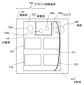
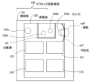
- FIGS. 15 and 16 are diagrams showing an example of a configuration in which an R-shape is provided at the end of the conductive plate.
- the ceramic circuit board 100 includes an insulating plate 110 formed on a metal plate (not shown), and a conductive plate 120 formed on the insulating plate 110. Terminals (not shown) are joined to conductive plate 120 by solders 130a-130d. Furthermore, the solders 130b and 130d are surrounded by a separation groove m0. Component areas 121 to 124 on the conductive plate 120 are areas where semiconductor chips are mounted.
- solder 130a under the terminal when the solder 130a under the terminal is in a molten state, there is a possibility that the solder 130a wets and spreads to the end eg0 of the conductive plate 120. For this reason, it is conceivable to take a measure to provide an R shape at the end eg0 of the conductive plate 120 where there is a high possibility that cracks may occur in the ceramic circuit board 100.
- the conventional measure of reducing stress concentration on the ceramic circuit board by processing the sides of the conductive plate into an R shape may be difficult to implement depending on the semiconductor chip mounting layout. Therefore, there is a need for a technique that effectively alleviates the stress concentration on the ceramic circuit board due to wetting and spreading of solder, without depending on the semiconductor chip mounting layout, and prevents the occurrence of cracks in the ceramic circuit board.
- the semiconductor device includes an insulating plate, a conductive plate provided on the insulating plate, and a terminal bonded to the conductive plate with a bonding material, and the bonding material is prevented from spreading to the end of the conductive plate. Equipped with a structure that allows Further, this structure is provided in a predetermined area near the end where the bonding material should not adhere. Furthermore, another semiconductor device is provided to solve the above problems.
- the semiconductor device includes an insulating plate, a conductive plate provided on the insulating plate, and a terminal bonded to the conductive plate with a bonding material, and the bonding material is prevented from spreading to the end of the conductive plate.
- the material is non-adhesive.
- stress concentration on the ceramic circuit board can be alleviated and cracks can be prevented from occurring in the ceramic circuit board.
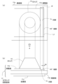
- FIG. 1 is a diagram showing an example of the configuration of a semiconductor device of the present invention.
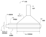
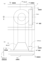
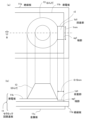
- FIG. 3 is a diagram showing the distance from the end of the conductive plate to the solder attachment area.
- FIG. 3 is a diagram showing the distance from the end of the conductive plate to the solder attachment area.
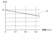
- FIG. 3 is a diagram showing the relationship between stress and the distance from the end of the conductive plate to the solder attachment area. It is a figure showing an example of an analysis result.
- FIG. 3 is a diagram showing an example of a structure for suppressing solder leakage and spread.
- FIG. 3 is a diagram showing an example of a structure for suppressing solder leakage and spread.
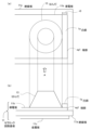
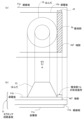
- Figure 7(a) shows a plan view of the ceramic circuit board seen from the front surface with solder below the terminals adhering to the conductive plate, and Figure 7(b) shows a side view of the ceramic circuit board seen from direction A. Show the diagram.
- FIG. 3 is a diagram showing an example of a structure for suppressing solder leakage and spread.
- FIG. 17(a) shows the structure before taking the measures
- FIG. 17(b) shows an example of the structure after taking the measures.
- FIG. 1 is a diagram showing an example of the configuration of a semiconductor device according to the present invention.
- a cross-sectional view of a semiconductor device 10 is shown.
- the semiconductor device 10 includes a ceramic circuit board 11, terminals 12 and 12-1 connected to the front surface of the ceramic circuit board 11, and a semiconductor chip 18.
- a bonding material leakage and spread suppression structure 1 for suppressing the leakage and spread of the molten solder 13 is provided near the end eg1 of the conductive plate 11b (details will be described later). Note that solder, brazing material, or the like is used as the bonding material 13, but in the following description, the bonding material will be described as solder.
- the wires 16-1 and 16-2 are made of a conductive metal such as copper or aluminum or a conductive alloy such as an iron-aluminum alloy, and are formed to have a diameter of 300 to 500 ⁇ m for a high voltage device. Ru.
- the ceramic circuit board 11 to which the semiconductor chip 18 is bonded is housed in a case 17, and a region surrounded by the case 17 and the base plate 15 is filled with a sealing resin 19 and sealed. Note that the case 17 and the base plate 15 are fixed with adhesive or the like.
- the metal plate 11c of the ceramic circuit board 11 is made of a conductive metal such as copper or aluminum and has a thickness of 0.1 to 1 mm, for example, and is provided on the lower surface of the insulating plate 11a.
- Such a semiconductor chip 18 includes, for example, a drain electrode (positive electrode, collector electrode in IGBT) and a source electrode (negative electrode, emitter electrode in IGBT) as main electrodes, and a gate electrode as a control electrode.
- the semiconductor chip 18 includes a diode element.
- the diode element is, for example, an FWD (Free Wheeling Diode) in which an SBD (Schottky Barrier Diode), a PiN (P-intrinsic-N) diode, or the like is provided antiparallel to a switching element.
- FWD Free Wheeling Diode
- SBD Schottky Barrier Diode
- PiN PiN diode
- the electronic components include, for example, a capacitor, a resistor, a thermistor, a current sensor, and a control IC (Integrated Circuit).
- the solder 13 is less likely to generate voids and has high temperature resistance.
- such solder 13 is an alloy whose main components are tin and antimony.
- the sealing resin 19 can be a gel filler.
- FIGS. 2 to 5 are diagrams showing the distance from the end of the conductive plate to the solder attachment area.
- the terminal 12 is bonded to the conductive plate 11b via the solder 13.
- FIG. 4 is a diagram showing the relationship between stress and the distance from the end of the conductive plate to the solder attachment area.
- the vertical axis is the stress applied to the ceramic circuit board 11, and the horizontal axis is the distance (mm) from the end eg1 of the conductive plate 11b to the solder 13 attachment area 12a.
- the line g1 shows the analysis results. As the distance from the end eg1 of the conductive plate 11b to the attachment area 12a of the solder 13 is increased, the stress becomes smaller and the possibility of cracking of the ceramic circuit board 11 is reduced.
- FIG. 5 is a diagram showing an example of the analysis results.
- FIG. 5 shows the analysis results in a table, and the items are the distance (mm) from the end eg1 of the conductive plate 11b to the adhesion area 12a of the solder 13, and the distance of stress generated in the ceramic circuit board 11. Indicates relative value (%) with respect to zero.
- FIG. 6 is a diagram showing an example of a structure for suppressing solder leakage and spread.
- Figure 6(a) shows a plan view of the ceramic circuit board seen from the front surface with solder below the terminals adhering to the conductive plate
- Figure 6(b) shows a side view of the ceramic circuit board seen from direction A. Show the diagram.
- a convex portion 1a is provided in a predetermined region r0 near the end portion eg1 where the solder 13 should not adhere to the conductive plate 11b, resulting in a convex structure.
- the convex portion 1a is made of, for example, a resin with high heat resistance that does not peel or deteriorate at the heating temperature of soldering, and a thermosetting resin can be used.
- the thermosetting resin include epoxy resin, phenol resin, maleimide resin, polyester resin, polyimide resin, silicone resin, and polyamide resin.
- the protrusion 1a is a metal wire.
- a dam wire can also be formed by joining a metal wire to a predetermined region r0 near the end eg1 of the conductive plate 11b.
- the material of the metal wire is, for example, gold, silver, copper, aluminum, or an alloy containing at least one of these. Bonding to the conductive plate 11b can be performed, for example, by ultrasonic bonding.
- FIG. 7 is a diagram showing an example of a structure for suppressing solder leakage and spread.
- Figure 7(a) shows a plan view of the ceramic circuit board seen from the front surface with solder below the terminals adhering to the conductive plate
- Figure 7(b) shows a side view of the ceramic circuit board seen from direction A. Show the diagram.
- a liquid repellent portion (resist) 1b is provided in a predetermined region r0 near the end portion eg1 where the solder 13 should not adhere to the conductive plate 11b.
- the liquid repellent portion 1b is an oxide film formed by oxidizing the conductive plate 11b.
- the oxide film is, for example, a nickel oxide film.
- Such an oxide film is formed by oxidizing the plating film by laser irradiating the plating film on the conductive plate 11b.
- the laser irradiation may be performed using either a CW laser that continuously emits laser light or a pulsed laser that emits laser light intermittently.
- FIG. 8 is a diagram showing an example of a structure for suppressing solder leakage and spread.
- Figure 8(a) shows a plan view of the ceramic circuit board seen from the front surface with solder below the terminals adhering to the conductive plate
- Figure 8(b) shows a side view of the ceramic circuit board seen from direction A. Show the diagram.
- solder leakage spread suppression structure #2> a structure for suppressing the spread of the solder 13 to the end eg1 of the conductive plate 11b will be described with reference to FIGS. 9 to 14.
- the solder leakage spread suppression structure shown in FIGS. 9, 11, and 13 has a structure in which a thinner portion of the conductive plate 11b is provided at the end eg1 of the conductive plate 11b.
- FIG. 9 is a diagram showing an example of a structure for suppressing solder leakage and spread.
- Figure 9(a) shows a plan view of the ceramic circuit board seen from the front surface with solder below the terminals adhering to the conductive plate
- Figure 9(b) shows a cross-sectional view of the ceramic circuit board seen from direction B. Show the front view.
- a step portion 1d is provided in a predetermined region r1 near the end portion eg1 where the solder 13 should not adhere to the conductive plate 11b, thereby forming a thinner portion of the conductive plate 11b.
- a step portion 1d having a step width of 0.15 mm is formed with respect to an end portion eg1 having a width of 5 mm in the conductive plate 11b.
- FIG. 10 is a diagram showing an example of the analysis results.
- FIG. 10 is a table showing the analysis results of the solder leakage spread suppressing structure shown in FIG. Indicates the relative value (%) of the stress generated at , based on the zero distance.
- FIG. 11 is a diagram showing an example of a structure for suppressing solder leakage and spread.
- Figure 11(a) shows a plan view of the ceramic circuit board seen from the front surface with solder below the terminals adhering to the conductive plate
- Figure 11(b) shows a cross-sectional view of the ceramic circuit board seen from direction B. Show the front view.
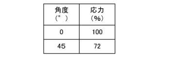
- FIG. 12 is a diagram showing an example of the analysis results.
- FIG. 12 is a table showing the analysis results of the solder leakage spread suppressing structure shown in FIG. 11, and the items are the angle (°) of the slope portion 1e, and the angle of stress generated in the ceramic circuit board 11, with the angle being zero. The relative value (%) is shown.
- FIG. 13 is a diagram showing an example of a structure for suppressing solder leakage and spread.
- Figure 13(a) shows a plan view of the ceramic circuit board seen from the front surface with solder below the terminals adhering to the conductive plate
- Figure 13(b) shows a cross-sectional view of the ceramic circuit board seen from direction B. Show the front view.
- a local stepped portion 1d1 is provided to form a thinner part of the conductive plate 11b.
- a step portion 1d1 having a step width of 0.15 mm is formed with respect to an end portion eg1 having a width of 1 mm of the conductive plate 11b.
- FIG. 14 is a diagram showing an example of the analysis results.
- Figure 14 is a table showing the analysis results of the solder leakage spread suppression structure shown in Figure 13, and the items are the distance (mm) from the end of the conductive plate to the solder attachment area, and the stress generated on the ceramic circuit board. Indicates the relative value (%) based on the zero distance.
- the stress is reduced by 13% compared to the case where the distance from the end eg1 of the conductive plate 11b to the solder 13 attachment area is 0 mm.
- the margin is slightly lower than in the case of FIG. 9, cracks in the ceramic circuit board 11 can be prevented by providing a local stepped portion 1d1 as shown in FIG.
Landscapes
- Structure Of Printed Boards (AREA)
- Chemical & Material Sciences (AREA)
- Engineering & Computer Science (AREA)
- Ceramic Engineering (AREA)
- Electric Connection Of Electric Components To Printed Circuits (AREA)
- Cooling Or The Like Of Semiconductors Or Solid State Devices (AREA)
Abstract
Description
しかし、セラミック回路基板のクラックが発生しうる周辺部における半導体チップ搭載レイアウトに余裕がないと、導電板の端部にR形状を設けるといった対策を施すことが難しいという問題がある。
また、上記課題を解決するために、他の半導体装置が提供される。半導体装置は、絶縁板と、絶縁板上に設けられた導電板と、導電板に接合材によって接合された端子とを備え、導電板の端部に、接合材が端部まで広がることを抑制する構造を備える。また、この構造として導電板の端部に導電板の厚さが薄い部分が設けられ、導電板の厚さが薄い部分の境界まで接合材は付着し、導電板の厚さが薄い部分は接合材が非付着となっている。
本発明の上記および他の目的、特徴および利点は本発明の例として好ましい実施の形態を表す添付の図面と関連した以下の説明により明らかになるであろう。
図1は本発明の半導体装置の構成の一例を示す図である。半導体装置10の横断面図を示している。半導体装置10は、セラミック回路基板11、セラミック回路基板11のおもて面に接続された端子12、12-1および半導体チップ18を有している。
次に図2から図5を用いて、導電板の端部からはんだの付着領域までの距離と応力との関係について説明する。図2、図3は導電板の端部からはんだの付着領域までの距離を示す図である。図2、図3それぞれの状態st1、st2では、はんだ13を介して端子12が導電板11bに接合されている状態が示されている。
次にはんだ13が導電板11bの端部eg1まで広がることを抑制する構造について、図6から図8を用いて説明する。図6ははんだ漏れ広がり抑制構造の一例を示す図である。図6(a)は端子下のはんだが導電板に付着しているセラミック回路基板をおもて面から見た平面図を示し、図6(b)はセラミック回路基板をA方向から見た側面図を示す。
次にはんだ13が導電板11bの端部eg1まで広がることを抑制する構造について、図9から図14を用いて説明する。なお、図9、図11、図13に示すはんだ漏れ広がり抑制構造は、導電板11bの端部eg1に、導電板11bの厚さが薄い部分を設けている構造を有するものである。
上記については単に本発明の原理を示すものである。さらに、多数の変形、変更が当業者にとって可能であり、本発明は上記に示し、説明した正確な構成および応用例に限定されるものではなく、対応するすべての変形例および均等物は、添付の請求項およびその均等物による本発明の範囲とみなされる。
11 セラミック回路基板
11a 絶縁板
11b、11b-1 導電板
11c 金属板
12、12-1 端子
13 接合材(はんだ)
15 ベースプレート
16-1、16-2 ワイヤ(ボンディングワイヤ)
17 ケース
18 半導体チップ
19 封止樹脂
eg1 端部
1 接合材漏れ広がり抑制構造
1a 凸部
1b 撥液部
1c 凹部
1d、1d1 段差部
1e 勾配部
st1、st2 状態
12a 付着領域
12b 非付着領域
g1 線
r0、r1、r2 所定領域
da 所定距離
L1 辺
Sr 応力値
Claims (11)
- 絶縁板と、
前記絶縁板上に設けられた導電板と、
前記導電板に接合材によって接合された端子と、を備え、
前記導電板の端部に、前記接合材が前記端部まで広がることを抑制する構造を備え、
前記構造は前記接合材を非付着とすべき前記端部の近傍の所定領域に設けられる、
半導体装置。 - 前記構造は凸状である、請求項1に記載の半導体装置。
- 前記凸状の構造は樹脂からなる、請求項2に記載の半導体装置。
- 前記凸状の構造は金属ワイヤを接合した部材である、請求項2に記載の半導体装置。
- 前記構造は前記所定領域が酸化された撥液部である、請求項1に記載の半導体装置。
- 前記撥液部は前記所定領域がレーザ照射による酸化膜である、請求項5に記載の半導体装置。
- 前記構造は凹状であり、前記導電板の前記端部から所定距離離れた位置に設けられる、請求項1に記載の半導体装置。
- 前記凹状の構造は前記導電板の前記端部の辺に沿って設けられた長孔である、請求項7に記載の半導体装置。
- 絶縁板と、
前記絶縁板上に設けられた導電板と、
前記導電板に接合材によって接合された端子と、を備え、
前記導電板の端部に、前記接合材が前記端部まで広がることを抑制する構造を備え、
前記構造として前記導電板の端部に前記導電板の厚さが薄い部分が設けられ、前記導電板の厚さが薄い部分の境界まで前記接合材は付着し、前記導電板の厚さが薄い部分は前記接合材が非付着となっている、
半導体装置。 - 前記導電板の厚さが薄い部分は、前記接合材を非付着とすべき前記端部の近傍の所定領域に設けられた段差である、請求項9に記載の半導体装置。
- 前記導電板の厚さが薄い部分は、前記接合材を非付着とすべき前記端部の近傍の所定領域に設けられた勾配である、請求項9に記載の半導体装置。
Priority Applications (3)
| Application Number | Priority Date | Filing Date | Title |
|---|---|---|---|
| JP2024528375A JP7761148B2 (ja) | 2022-06-13 | 2023-05-08 | 半導体装置 |
| CN202380014706.0A CN118318304A (zh) | 2022-06-13 | 2023-05-08 | 半导体装置 |
| US18/678,778 US20240321675A1 (en) | 2022-06-13 | 2024-05-30 | Semiconductor device |
Applications Claiming Priority (2)
| Application Number | Priority Date | Filing Date | Title |
|---|---|---|---|
| JP2022095159 | 2022-06-13 | ||
| JP2022-095159 | 2022-06-13 |
Related Child Applications (1)
| Application Number | Title | Priority Date | Filing Date |
|---|---|---|---|
| US18/678,778 Continuation US20240321675A1 (en) | 2022-06-13 | 2024-05-30 | Semiconductor device |
Publications (1)
| Publication Number | Publication Date |
|---|---|
| WO2023243256A1 true WO2023243256A1 (ja) | 2023-12-21 |
Family
ID=89191005
Family Applications (1)
| Application Number | Title | Priority Date | Filing Date |
|---|---|---|---|
| PCT/JP2023/017306 Ceased WO2023243256A1 (ja) | 2022-06-13 | 2023-05-08 | 半導体装置 |
Country Status (4)
| Country | Link |
|---|---|
| US (1) | US20240321675A1 (ja) |
| JP (1) | JP7761148B2 (ja) |
| CN (1) | CN118318304A (ja) |
| WO (1) | WO2023243256A1 (ja) |
Citations (8)
| Publication number | Priority date | Publication date | Assignee | Title |
|---|---|---|---|---|
| JPH07221265A (ja) * | 1994-01-28 | 1995-08-18 | Hitachi Ltd | パワー半導体モジュール |
| JP2004363216A (ja) * | 2003-06-03 | 2004-12-24 | Fuji Electric Holdings Co Ltd | 半導体装置 |
| WO2015151273A1 (ja) * | 2014-04-04 | 2015-10-08 | 三菱電機株式会社 | 半導体装置 |
| JP2017017204A (ja) * | 2015-07-02 | 2017-01-19 | 三菱電機株式会社 | 半導体装置の製造方法 |
| JP2017188534A (ja) * | 2016-04-04 | 2017-10-12 | 株式会社デンソー | 電子装置及びその製造方法 |
| JP2021002637A (ja) * | 2019-06-21 | 2021-01-07 | 富士電機株式会社 | 半導体装置及び半導体装置の製造方法 |
| JP2021077790A (ja) * | 2019-11-11 | 2021-05-20 | 三菱電機株式会社 | 半導体装置の製造方法 |
| JP2021118350A (ja) * | 2020-01-23 | 2021-08-10 | 富士電機株式会社 | 電子装置及び電子装置の製造方法 |
Family Cites Families (1)
| Publication number | Priority date | Publication date | Assignee | Title |
|---|---|---|---|---|
| JP6952503B2 (ja) * | 2017-06-07 | 2021-10-20 | 三菱電機株式会社 | 半導体装置の製造方法 |
-
2023
- 2023-05-08 JP JP2024528375A patent/JP7761148B2/ja active Active
- 2023-05-08 WO PCT/JP2023/017306 patent/WO2023243256A1/ja not_active Ceased
- 2023-05-08 CN CN202380014706.0A patent/CN118318304A/zh active Pending
-
2024
- 2024-05-30 US US18/678,778 patent/US20240321675A1/en active Pending
Patent Citations (8)
| Publication number | Priority date | Publication date | Assignee | Title |
|---|---|---|---|---|
| JPH07221265A (ja) * | 1994-01-28 | 1995-08-18 | Hitachi Ltd | パワー半導体モジュール |
| JP2004363216A (ja) * | 2003-06-03 | 2004-12-24 | Fuji Electric Holdings Co Ltd | 半導体装置 |
| WO2015151273A1 (ja) * | 2014-04-04 | 2015-10-08 | 三菱電機株式会社 | 半導体装置 |
| JP2017017204A (ja) * | 2015-07-02 | 2017-01-19 | 三菱電機株式会社 | 半導体装置の製造方法 |
| JP2017188534A (ja) * | 2016-04-04 | 2017-10-12 | 株式会社デンソー | 電子装置及びその製造方法 |
| JP2021002637A (ja) * | 2019-06-21 | 2021-01-07 | 富士電機株式会社 | 半導体装置及び半導体装置の製造方法 |
| JP2021077790A (ja) * | 2019-11-11 | 2021-05-20 | 三菱電機株式会社 | 半導体装置の製造方法 |
| JP2021118350A (ja) * | 2020-01-23 | 2021-08-10 | 富士電機株式会社 | 電子装置及び電子装置の製造方法 |
Also Published As
| Publication number | Publication date |
|---|---|
| JP7761148B2 (ja) | 2025-10-28 |
| US20240321675A1 (en) | 2024-09-26 |
| CN118318304A (zh) | 2024-07-09 |
| JPWO2023243256A1 (ja) | 2023-12-21 |
Similar Documents
| Publication | Publication Date | Title |
|---|---|---|
| CN112166506B (zh) | 半导体装置 | |
| US7816784B2 (en) | Power quad flat no-lead semiconductor die packages with isolated heat sink for high-voltage, high-power applications, systems using the same, and methods of making the same | |
| US10943859B2 (en) | Semiconductor device | |
| US8466548B2 (en) | Semiconductor device including excess solder | |
| US12040301B2 (en) | Semiconductor device | |
| CN105917463B (zh) | 半导体装置 | |
| JPWO2019244492A1 (ja) | 半導体装置 | |
| JP2025100870A (ja) | 半導体装置 | |
| JP7729368B2 (ja) | 半導体装置 | |
| JP7540248B2 (ja) | 半導体モジュール | |
| JP2019212808A (ja) | 半導体装置の製造方法 | |
| US12506043B2 (en) | Semiconductor device | |
| JP7365368B2 (ja) | 半導体装置 | |
| US10236244B2 (en) | Semiconductor device and production method therefor | |
| JP7761148B2 (ja) | 半導体装置 | |
| CN116711073A (zh) | 半导体装置以及半导体装置的制造方法 | |
| US11587879B2 (en) | Electronic apparatus and manufacturing method thereof | |
| US20240071898A1 (en) | Semiconductor device and semiconductor device manufacturing method | |
| JP7836715B2 (ja) | 半導体モジュール及び電力変換装置 | |
| US12327808B2 (en) | Semiconductor device | |
| US11996347B2 (en) | Semiconductor device | |
| US11337306B2 (en) | Semiconductor device | |
| US20250385213A1 (en) | Semiconductor device and manufacturing method therefor | |
| JP2025165150A (ja) | 半導体モジュール | |
| JP2025104605A (ja) | 半導体モジュールおよび製造方法 |
Legal Events
| Date | Code | Title | Description |
|---|---|---|---|
| 121 | Ep: the epo has been informed by wipo that ep was designated in this application |
Ref document number: 23823559 Country of ref document: EP Kind code of ref document: A1 |
|
| WWE | Wipo information: entry into national phase |
Ref document number: 202380014706.0 Country of ref document: CN |
|
| WWE | Wipo information: entry into national phase |
Ref document number: 2024528375 Country of ref document: JP |
|
| NENP | Non-entry into the national phase |
Ref country code: DE |
|
| 122 | Ep: pct application non-entry in european phase |
Ref document number: 23823559 Country of ref document: EP Kind code of ref document: A1 |