WO2023238745A1 - 窒化物半導体装置 - Google Patents
窒化物半導体装置 Download PDFInfo
- Publication number
- WO2023238745A1 WO2023238745A1 PCT/JP2023/020198 JP2023020198W WO2023238745A1 WO 2023238745 A1 WO2023238745 A1 WO 2023238745A1 JP 2023020198 W JP2023020198 W JP 2023020198W WO 2023238745 A1 WO2023238745 A1 WO 2023238745A1
- Authority
- WO
- WIPO (PCT)
- Prior art keywords
- gate
- layer
- nitride semiconductor
- gate electrode
- semiconductor device
- Prior art date
- Legal status (The legal status is an assumption and is not a legal conclusion. Google has not performed a legal analysis and makes no representation as to the accuracy of the status listed.)
- Ceased
Links
Images



Classifications
-
- H—ELECTRICITY
- H10—SEMICONDUCTOR DEVICES; ELECTRIC SOLID-STATE DEVICES NOT OTHERWISE PROVIDED FOR
- H10D—INORGANIC ELECTRIC SEMICONDUCTOR DEVICES
- H10D30/00—Field-effect transistors [FET]
- H10D30/01—Manufacture or treatment
- H10D30/061—Manufacture or treatment of FETs having Schottky gates
-
- H—ELECTRICITY
- H10—SEMICONDUCTOR DEVICES; ELECTRIC SOLID-STATE DEVICES NOT OTHERWISE PROVIDED FOR
- H10D—INORGANIC ELECTRIC SEMICONDUCTOR DEVICES
- H10D30/00—Field-effect transistors [FET]
- H10D30/01—Manufacture or treatment
- H10D30/051—Manufacture or treatment of FETs having PN junction gates
-
- H—ELECTRICITY
- H10—SEMICONDUCTOR DEVICES; ELECTRIC SOLID-STATE DEVICES NOT OTHERWISE PROVIDED FOR
- H10D—INORGANIC ELECTRIC SEMICONDUCTOR DEVICES
- H10D30/00—Field-effect transistors [FET]
- H10D30/40—FETs having zero-dimensional [0D], one-dimensional [1D] or two-dimensional [2D] charge carrier gas channels
- H10D30/47—FETs having zero-dimensional [0D], one-dimensional [1D] or two-dimensional [2D] charge carrier gas channels having two-dimensional [2D] charge carrier gas channels, e.g. nanoribbon FETs or high electron mobility transistors [HEMT]
- H10D30/471—High electron mobility transistors [HEMT] or high hole mobility transistors [HHMT]
-
- H—ELECTRICITY
- H10—SEMICONDUCTOR DEVICES; ELECTRIC SOLID-STATE DEVICES NOT OTHERWISE PROVIDED FOR
- H10D—INORGANIC ELECTRIC SEMICONDUCTOR DEVICES
- H10D30/00—Field-effect transistors [FET]
- H10D30/80—FETs having rectifying junction gate electrodes
- H10D30/83—FETs having PN junction gate electrodes
-
- H—ELECTRICITY
- H10—SEMICONDUCTOR DEVICES; ELECTRIC SOLID-STATE DEVICES NOT OTHERWISE PROVIDED FOR
- H10D—INORGANIC ELECTRIC SEMICONDUCTOR DEVICES
- H10D30/00—Field-effect transistors [FET]
- H10D30/80—FETs having rectifying junction gate electrodes
- H10D30/87—FETs having Schottky gate electrodes, e.g. metal-semiconductor FETs [MESFET]
-
- H—ELECTRICITY
- H10—SEMICONDUCTOR DEVICES; ELECTRIC SOLID-STATE DEVICES NOT OTHERWISE PROVIDED FOR
- H10D—INORGANIC ELECTRIC SEMICONDUCTOR DEVICES
- H10D64/00—Electrodes of devices having potential barriers
- H10D64/20—Electrodes characterised by their shapes, relative sizes or dispositions
-
- H—ELECTRICITY
- H10—SEMICONDUCTOR DEVICES; ELECTRIC SOLID-STATE DEVICES NOT OTHERWISE PROVIDED FOR
- H10D—INORGANIC ELECTRIC SEMICONDUCTOR DEVICES
- H10D64/00—Electrodes of devices having potential barriers
- H10D64/20—Electrodes characterised by their shapes, relative sizes or dispositions
- H10D64/27—Electrodes not carrying the current to be rectified, amplified, oscillated or switched, e.g. gates
-
- H—ELECTRICITY
- H10—SEMICONDUCTOR DEVICES; ELECTRIC SOLID-STATE DEVICES NOT OTHERWISE PROVIDED FOR
- H10D—INORGANIC ELECTRIC SEMICONDUCTOR DEVICES
- H10D62/00—Semiconductor bodies, or regions thereof, of devices having potential barriers
- H10D62/80—Semiconductor bodies, or regions thereof, of devices having potential barriers characterised by the materials
- H10D62/83—Semiconductor bodies, or regions thereof, of devices having potential barriers characterised by the materials being Group IV materials, e.g. B-doped Si or undoped Ge
Definitions
- the present disclosure relates to a nitride semiconductor device.
- nitride semiconductor device which is a HEMT, is made of a nitride semiconductor, and includes a gate layer formed on an electron supply layer, a gate electrode formed on the gate layer, Equipped with. Further, the nitride semiconductor device includes a passivation film that covers the gate layer and the gate electrode.
- a nitride semiconductor device includes: an electron supply layer made of a nitride semiconductor; a gate layer formed on a portion of the electron supply layer made of a nitride semiconductor containing acceptor-type impurities; A gate electrode formed on a gate layer and having a width, and a passivation film covering the gate layer and the gate electrode, the gate electrode having a lower gate surface in contact with the gate layer and a side opposite to the lower gate surface. and a gate side surface connecting the gate bottom surface and the gate top surface, the gate side surface having a first side surface that is continuous with the gate top surface, and a gate side surface that is closer to the gate than the first side surface.
- a second side surface portion provided on a lower surface side, and a first angle of the first side surface portion with respect to the width direction of the gate electrode is smaller than a second angle of the second side surface portion with respect to the width direction.
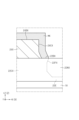
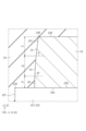
- FIG. 1 is a schematic plan view of an exemplary nitride semiconductor device according to one embodiment.
- FIG. 2 is a schematic cross-sectional view of the nitride semiconductor device taken along line F2-F2 in FIG.
- FIG. 3 is an enlarged view of section F3 in FIG. 2.
- FIG. 4 is an enlarged view of the gate electrode in FIG. 3 and its surroundings.
- FIG. 5 is an enlarged view of a gate electrode and its surroundings in a nitride semiconductor device of a comparative example.
- FIG. 6 is an explanatory diagram illustrating an example of a manufacturing process of a nitride semiconductor device of a comparative example.
- FIG. 1 is a schematic plan view of an exemplary nitride semiconductor device according to one embodiment.
- FIG. 2 is a schematic cross-sectional view of the nitride semiconductor device taken along line F2-F2 in FIG.
- FIG. 3 is an enlarged view of section F3 in FIG. 2.
- FIG. 4 is
- FIG. 7 is an enlarged schematic cross-sectional view of a gate electrode and its surroundings in a modified nitride semiconductor device.
- FIG. 8 is an enlarged schematic cross-sectional view of a gate electrode and its surroundings in a modified nitride semiconductor device.
- FIG. 1 shows a schematic planar structure of a nitride semiconductor device 10 according to this embodiment.
- FIG. 2 shows a schematic cross-sectional structure of the nitride semiconductor device 10 of FIG. 1 taken along line F2-F2 of FIG.
- the term "planar view” used in the present disclosure refers to viewing the nitride semiconductor device 10 in the Z-axis direction of the mutually orthogonal XYZ axes shown in FIGS. 1 and 2.
- the +Z direction is defined as top, the -Z direction as bottom, the +X direction as right, and the -X direction as left.
- planear view refers to viewing nitride semiconductor device 10 from above along the Z-axis.
- the nitride semiconductor device 10 is a high electron mobility transistor (HEMT) using a nitride semiconductor.
- the nitride semiconductor device 10 includes a semiconductor substrate 12, a buffer layer 14 formed on the semiconductor substrate 12, an electron transit layer 16 formed on the buffer layer 14, and an electron supply layer formed on the electron transit layer 16. layer 18.
- a silicon (Si) substrate can be used.
- a silicon carbide (SiC) substrate, a gallium nitride (GaN) substrate, or a sapphire substrate can be used instead of the Si substrate.
- the thickness of the semiconductor substrate 12 can be, for example, 200 ⁇ m or more and 1500 ⁇ m or less. In the following description, unless explicitly stated otherwise, thickness refers to a dimension along the Z-axis direction in FIG. 2.
- the buffer layer 14 may be made of any material that can suppress wafer warping and cracking due to mismatch in thermal expansion coefficients between the semiconductor substrate 12 and the electron transit layer 16. Additionally, buffer layer 14 can include one or more nitride semiconductor layers. Buffer layer 14 may include, for example, at least one of an aluminum nitride (AlN) layer, an aluminum gallium nitride (AlGaN) layer, and a graded AlGaN layer with a different aluminum (Al) composition.
- AlN aluminum nitride
- AlGaN aluminum gallium nitride
- AlGaN graded AlGaN layer with a different aluminum
- the buffer layer 14 is made of a single film of AlN, a single film of AlGaN, a film having an AlGaN/GaN superlattice structure, a film having an AlN/AlGaN superlattice structure, a film having an AlN/GaN superlattice structure, or the like. may have been done.
- the buffer layer 14 includes a first buffer layer that is an AlN layer formed on the semiconductor substrate 12 and a second buffer layer that is an AlGaN layer formed on the AlN layer (first buffer layer). I can do it.
- the first buffer layer may be, for example, an AlN layer with a thickness of 200 nm
- the second buffer layer may be a graded AlGaN layer, for example, with a thickness of 300 nm.
- impurities may be introduced into a portion of the buffer layer 14 to make the buffer layer 14 semi-insulating except for the surface layer region.
- the impurity is, for example, carbon (C) or iron (Fe).
- the impurity concentration can be, for example, 4 ⁇ 10 16 cm ⁇ 3 or higher.
- the electron transit layer 16 is made of a nitride semiconductor.
- the electron transit layer 16 may be, for example, a GaN layer.
- the thickness of the electron transit layer 16 can be, for example, 0.5 ⁇ m or more and 2 ⁇ m or less.
- impurities may be introduced into a part of the electron transit layer 16 to make the region other than the surface layer of the electron transit layer 16 semi-insulating.
- the impurity is, for example, C.
- the concentration of impurities can be, for example, 4 ⁇ 10 16 cm ⁇ 3 or more.
- the electron transit layer 16 can include a plurality of GaN layers having different impurity concentrations, for example, a C-doped GaN layer and a non-doped GaN layer.
- a C-doped GaN layer is formed on the buffer layer 14.
- the C-doped GaN layer can have a thickness of 0.5 ⁇ m or more and 2 ⁇ m or less.
- the C concentration in the C-doped GaN layer can be set to 5 ⁇ 10 17 cm ⁇ 3 or more and 9 ⁇ 10 19 cm ⁇ 3 or less.
- the non-doped GaN layer is formed on the C-doped GaN layer.
- the undoped GaN layer can have a thickness of 0.05 ⁇ m or more and 0.4 ⁇ m or less.
- the non-doped GaN layer is in contact with the electron supply layer 18.
- the electron transit layer 16 includes a C-doped GaN layer with a thickness of 0.4 ⁇ m and a non-doped GaN layer with a thickness of 0.4 ⁇ m.
- the C concentration in the C-doped GaN layer is approximately 2 ⁇ 10 19 cm ⁇ 3 .
- the electron supply layer 18 has a larger band gap than the electron transit layer 16.
- the electron supply layer 18 may be, for example, an AlGaN layer. In a nitride semiconductor, the higher the Al composition, the larger the band gap. Therefore, the electron supply layer 18, which is an AlGaN layer, has a larger band gap than the electron transit layer 16, which is a GaN layer.
- the electron supply layer 18 is composed of Al x Ga 1-x N. In other words, the electron supply layer 18 can be said to be an Al x Ga 1-x N layer. x is 0 ⁇ x ⁇ 0.4, more preferably 0.1 ⁇ x ⁇ 0.3.
- the electron supply layer 18 can have a thickness of, for example, 5 nm or more and 20 nm or less.
- the electron transit layer 16 and the electron supply layer 18 have different lattice constants in the bulk region. Therefore, the electron transit layer 16 and the electron supply layer 18 are a lattice mismatched junction.
- the heterojunction interface between the electron transit layer 16 and the electron supply layer 18 is caused by the spontaneous polarization of the electron transit layer 16 and the electron supply layer 18 and the piezo polarization caused by the compressive stress that the heterojunction of the electron transit layer 16 receives.
- the energy level of the conduction band of the electron transport layer 16 in the vicinity is lower than the Fermi level.
- two-dimensional electron gas (2DEG) 20 spreads within the electron transit layer 16 at a position close to the heterojunction interface between the electron transit layer 16 and the electron supply layer 18 (for example, at a distance of several nm from the interface). There is.
- the nitride semiconductor device 10 includes a gate layer 22 formed on the electron supply layer 18 , a gate electrode 24 formed on the gate layer 22 , and a passivation layer covering the electron supply layer 18 , the gate layer 22 , and the gate electrode 24 .
- a membrane 26 is further included.
- the passivation film 26 has a source opening 26A and a drain opening 26B provided on both sides of the gate layer 22 in the X-axis direction in a plan view.
- the gate layer 22 has a smaller band gap than the electron supply layer 18 and is made of a nitride semiconductor containing acceptor type impurities.
- Gate layer 22 may be comprised of any material having a smaller bandgap than electron supply layer 18, for example an AlGaN layer.
- the gate layer 22 is a GaN layer doped with acceptor type impurities (p-type GaN layer).
- the acceptor type impurity can include at least one of zinc (Zn), magnesium (Mg), and C.
- the maximum concentration of acceptor type impurities in the gate layer 22 is, for example, 1 ⁇ 10 18 cm ⁇ 3 or more and 1 ⁇ 10 20 cm ⁇ 3 or less.
- the energy level of the electron transport layer 16 and the electron supply layer 18 is raised. Therefore, in the region immediately below the gate layer 22, the energy level of the conduction band of the electron transit layer 16 near the heterojunction interface between the electron transit layer 16 and the electron supply layer 18 is approximately the same as the Fermi level, or Or even bigger. Therefore, at zero bias when no voltage is applied to the gate electrode 24, the 2DEG 20 is not formed in the electron transit layer 16 in the region directly under the gate layer 22. On the other hand, a 2DEG 20 is formed in the electron transit layer 16 in a region other than the region immediately below the gate layer 22.
- the presence of the gate layer 22 doped with acceptor type impurities causes the 2DEG 20 to be depleted in the region immediately below the gate layer 22.
- normally-off operation of the nitride semiconductor device 10 is realized.
- an appropriate on-voltage is applied to the gate electrode 24, a channel is formed by the 2DEG 20 in the electron transit layer 16 in the region immediately below the gate electrode 24, so that conduction occurs between the source and the drain.
- the gate layer 22 includes a bottom surface 22A in contact with the electron supply layer 18 and a top surface 22B on the opposite side from the bottom surface 22A.
- the gate electrode 24 is formed on the upper surface 22B of the gate layer 22.
- the gate layer 22 can have a rectangular, trapezoidal, or ridge-shaped cross section in the XZ plane in FIG. 2 .
- the gate layer 22 includes a gate ridge portion 22C including an upper surface 22B on which the gate electrode 24 is formed, and two gate extension portions (a first gate extension portion) extending outside the gate ridge portion 22C in plan view. portion 22D and second gate extension portion 22E). Therefore, the upper surface 22B of the gate layer 22 refers to the upper surface formed in the gate ridge portion 22C.
- the first gate extension portion 22D extends from the gate ridge portion 22C toward the source opening portion 26A in plan view.
- the first gate extension 22D is spaced apart from the source opening 26A.
- the second gate extension portion 22E extends from the gate ridge portion 22C toward the drain opening 26B in plan view.
- the second gate extension 22E is spaced apart from the drain opening 26B.
- the gate ridge portion 22C is located between the first gate extension portion 22D and the second gate extension portion 22E, and is formed integrally with the first gate extension portion 22D and the second gate extension portion 22E.
- the first gate extension portion 22D and the second gate extension portion 22E are formed to sandwich the gate ridge portion 22C in the width direction of the gate ridge portion 22C (in the X-axis direction in FIG. 2).
- the width direction of the gate ridge portion 22C is a direction perpendicular to the direction in which the gate ridge portion 22C extends in plan view.
- the bottom surface 22A of the gate layer 22 has a larger area than the top surface 22B.
- the second gate extension part 22E extends longer toward the outside of the gate ridge part 22C in plan view than the first gate extension part 22D.
- the gate ridge portion 22C corresponds to a relatively thick portion of the gate layer 22.
- the thickness of the gate layer 22, particularly the gate ridge portion 22C can be determined in consideration of parameters including the gate threshold voltage.
- the thickness T1 (see FIG. 3) of the gate layer 22 is greater than or equal to 110 nm and less than or equal to 150 nm.
- the thickness T1 of the gate layer 22 can be defined by the distance between the top surface 22B and bottom surface 22A of the gate ridge portion 22C in the Z-axis direction.
- each of the first gate extension part 22D and the second gate extension part 22E has a thickness smaller than the thickness of the gate ridge part 22C.
- each of the first gate extension part 22D and the second gate extension part 22E has a thickness that is 1/2 or less of the thickness of the gate ridge part 22C.
- each gate extension portion 22D, 22E is a flat portion having a substantially constant thickness.
- substantially constant thickness refers to a thickness within a range of manufacturing variations (for example, 20%).
- the flat portion has a thickness of 5 nm or more and 25 nm or less.
- the gate electrode 24 has a width.
- the width of the gate electrode 24 can be defined by the size in a direction perpendicular to the direction in which the gate electrode 24 extends in plan view. Therefore, the width direction of the gate electrode 24 is a direction perpendicular to the direction in which the gate electrode 24 extends in plan view. In FIG. 2, the width direction of the gate electrode 24 is the X-axis direction.
- the gate electrode 24 includes a gate lower surface 24A in contact with the gate layer 22, a gate upper surface 24B opposite to the gate lower surface 24A, and a gate side surface 24C connecting the gate lower surface 24A and the gate upper surface 24B.
- Gate electrode 24 is composed of one or more metal layers.
- the gate electrode 24 is, for example, a titanium nitride (TiN) layer.
- the gate electrode 24 may include a first metal layer made of a material containing Ti, and a second metal layer laminated on the first metal layer and made of a material containing TiN. .
- the gate electrode 24 can form a Schottky junction with the gate layer 22.
- the thickness T2 see FIG.
- the gate electrode 24 is thicker than the thickness T1 of the gate layer 22, for example.
- the thickness T2 of the gate electrode 24 is greater than or equal to 100 nm and less than or equal to 200 nm.
- the thickness T2 of the gate electrode 24 can be defined by the distance between the gate upper surface 24B and the gate lower surface 24A of the gate electrode 24 in the Z-axis direction.
- the width W2 of the gate electrode 24 is smaller than the width W1 of the gate ridge portion 22C of the gate layer 22. In other words, the width W1 of the gate ridge portion 22C is larger than the width W2 of the gate electrode 24. In one example, the width W1 of the gate ridge portion 22C is smaller than twice the width W2 of the gate electrode 24. In one example, the width W1 of the gate ridge portion 22C is smaller than 1.5 times the width W2 of the gate electrode 24. In this way, it is preferable that the width W1 of the gate ridge portion 22C is as small as possible within a range larger than the width W2 of the gate electrode 24.
- the passivation film 26 is made of, for example, one of silicon nitride (SiN), silicon dioxide (SiO 2 ), silicon oxynitride (SiON), alumina (Al 2 O 3 ), AlN, and aluminum oxynitride (AlON). It can be constructed from materials that include.
- the passivation film 26 is formed of a material containing SiN.
- the portion of the passivation film 26 that covers the gate layer 22 and the gate electrode 24 is formed along the surfaces of the gate layer 22 and the gate electrode 24, and therefore has a non-flat surface.
- the thickness T3 of the passivation film 26 is, for example, 200 nm or less.
- the thickness T3 of the passivation film 26 may be, for example, the thickness of a portion in contact with the electron supply layer 18. Further, the thickness T3 of the passivation film 26 may be, for example, the thickness of a portion of the gate electrode 24 that is in contact with the gate upper surface 24B.
- Each of the source opening 26A and the drain opening 26B is spaced apart from the gate layer 22.
- Gate layer 22 is located between source opening 26A and drain opening 26B.
- source electrode 28 is in contact with electron supply layer 18 exposed by source opening 26A.
- the drain electrode 30 is in contact with the electron supply layer 18 exposed through the drain opening 26B.
- the gate layer 22 is arranged closer to the source opening 26A than the drain opening 26B in the X-axis direction. That is, the distance between the second gate extension 22E and the drain opening 26B in the X-axis direction is longer than the distance between the first gate extension 22D and the source opening 26A in the X-axis direction.
- the source electrode 28 and the drain electrode 30 are composed of one or more metal layers (eg, Ti, Al, AlCu, TiN, etc.). Source electrode 28 and drain electrode 30 are in ohmic contact with 2DEG 20 via source opening 26A and drain opening 26B, respectively.
- metal layers eg, Ti, Al, AlCu, TiN, etc.
- the source electrode 28 includes a source contact portion 28A and a source field plate portion 28B continuous with the source contact portion 28A.
- the source contact portion 28A corresponds to a portion filled in the source opening 26A.
- the source field plate portion 28B is formed integrally with the source contact portion 28A.
- the source field plate portion 28B covers the passivation film 26.
- Source field plate portion 28B includes an end portion 28C located between drain opening 26B and gate layer 22 in plan view. Therefore, the source field plate portion 28B is spaced apart from the drain electrode 30 formed in the drain opening 26B.
- the source field plate portion 28B extends along the surface of the passivation film 26 from the source contact portion 28A to the end portion 28C toward the drain electrode 30.
- the passivation film 26 covers the upper surface of the electron supply layer 18, the side surfaces 22F and upper surface 22B of the gate layer 22 (see FIG. 3), and the gate side surfaces 24C and upper gate surface 24B of the gate electrode 24. Therefore, the source field plate portion 28B extending along the surface of the passivation film 26 has a non-flat surface.
- the source field plate portion 28B plays a role of alleviating electric field concentration near the end of the gate electrode 24 at zero bias when no gate voltage is applied to the gate electrode 24.
- the drain electrode 30 includes a drain contact portion 30A and a drain plate portion 30B continuous to the drain contact portion 30A.
- the drain contact portion 30A corresponds to a portion filled in the drain opening 26B.
- the drain plate portion 30B is formed integrally with the drain contact portion 30A.
- the drain plate portion 30B covers the passivation film 26.
- the drain plate portion 30B is formed at the periphery of the drain opening 26B in the passivation film 26.
- nitride semiconductor device 10 includes an active region 40 that contributes to transistor operation and an inactive region 42 that does not contribute to transistor operation.
- active regions 40 and inactive regions 42 are arranged alternately in the Y-axis direction.
- Drain electrode 30 is formed in active region 40 .
- the active region 40 may extend to approximately the same extent as the drain electrode 30 in the Y-axis direction.
- the inactive region 42 may extend in the Y-axis direction to a range where the drain electrode 30 does not exist. Therefore, the inactive region 42 is adjacent to the active region 40 in the Y-axis direction.
- the source contact portion 28A of the source electrode 28, the gate layer 22 where the gate electrode 24 is located, and the drain electrode 30 are arranged adjacent to each other in the X-axis direction on the electron supply layer 18 (see FIG. 1). has been done.
- a combination of the source electrode 28, gate layer 22, gate electrode 24, and drain electrode 30 that are adjacent to each other in the X-axis direction constitutes one HEMT cell 10HC.
- two HEMT cells 10HC are arranged in each active region 40 in the X-axis direction. Note that, in reality, more HEMT cells 10HC may be arranged in each active region 40.
- the gate layer 22 is formed in a ring shape surrounding the drain electrode 30 in plan view. Therefore, the gate layer 22 is formed across the active region 40 and the inactive region 42 in the Y-axis direction.
- the gate electrode 24 formed on the gate layer 22 is formed in a ring shape surrounding the drain electrode 30 similarly to the gate layer 22 in plan view. Therefore, the gate electrode 24 is formed across the active region 40 and the inactive region 42 in the Y-axis direction.
- the source contact portion 28A of the source electrode 28 extends along the Y-axis direction.
- the length of the source contact portion 28A in the Y-axis direction is longer than the length of the drain electrode 30 in the Y-axis direction. Therefore, the source contact portion 28A is formed across the active region 40 and the inactive region 42 in the Y-axis direction.
- the length of the source contact portion 28A in the Y-axis direction is shorter than the length of the gate electrode 24 in the Y-axis direction.
- the source electrode 28 includes an opening 28D that constitutes an end 28C of the source field plate portion 28B.
- the opening 28D is formed in an annular shape surrounding the drain electrode 30 in plan view. Therefore, the opening 28D is formed over the entire active region 40 and a part of the inactive region 42 adjacent to the active region 40 in the Y-axis direction.
- the source field plate portion 28B is formed to cover both the gate layer 22 and the gate electrode 24 at least in the active region 40.
- the source field plate section 28B does not cover both the gate layer 22 and the gate electrode 24 in a part of the non-active region 42.
- the configuration of the source field plate section 28B can be arbitrarily changed, and in one example, the source field plate section 28B is configured to cover the entirety of both the gate layer 22 and the gate electrode 24 disposed in the inactive region 42. may be configured.
- FIG. 3 shows an enlarged cross-sectional structure of the gate electrode 24 and its surroundings as part F3, which is the region indicated by the dashed line in FIG.
- FIG. 4 shows an enlarged cross-sectional structure of a gate side surface 24C of the gate electrode 24 near the source electrode 28 and a part of the gate layer 22 in FIG.
- the gate side surface 24C of the gate electrode 24 includes a first side surface portion 32 that is continuous with the gate upper surface 24B, and a second side surface portion that is provided closer to the gate lower surface 24A than the first side surface portion 32. 34.
- the gate side surface 24C includes a third side surface section 36 provided between the first side surface section 32 and the second side surface section 34 in the Z-axis direction.
- the third side surface portion 36 connects the first side surface portion 32 and the second side surface portion 34.
- the second side surface portion 34 is the lowest side surface portion that is continuous with the gate lower surface 24A. That is, the second side surface portion 34 is in contact with the upper surface 22B of the gate layer 22.
- the Z-axis direction corresponds to the thickness direction of the gate electrode 24. Therefore, FIGS. 3 and 4 show a cross-sectional structure of the gate electrode 24 taken along a plane along the thickness direction and the width direction of the gate electrode 24.
- each of the first side surface portion 32, the second side surface portion 34, and the third side surface portion 36 is an inclined surface having an angle of less than 90° with respect to the width direction of the gate electrode 24, that is, the X-axis direction. .
- the gate side surface 24C includes a plurality of inclined surfaces.
- the X-axis direction may be used as the width direction of the gate electrode 24.
- the first angle ⁇ 1 of the first side surface portion 32 with respect to the X-axis direction is smaller than the second angle ⁇ 2 of the second side surface portion 34 with respect to the X-axis direction.
- the first angle ⁇ 1 is smaller than the third angle ⁇ 3 at the third side surface portion 36 with respect to the X-axis direction.
- the second angle ⁇ 2 is smaller than the third angle ⁇ 3.
- the third angle ⁇ 3 is larger than the second angle ⁇ 2.
- the first angle ⁇ 1 is, for example, 60° or more and 85° or less.
- the second angle ⁇ 2 is, for example, greater than 85° and less than 90°.
- the third angle ⁇ 3 is, for example, greater than 85° and less than 90°.
- each of the first angle ⁇ 1, the second angle ⁇ 2, and the third angle ⁇ 3 is less than 90°.
- the average value of the angles of the side surfaces 32, 34, and 36 forming the gate side surface 24C including the first side surface 32, the second side surface 34, and the third side surface 36 with respect to the X-axis direction is, for example, 70°.
- the angle is greater than or equal to 90°.
- the average value of the angles with respect to the X-axis direction of the side surfaces 32, 34, and 36 forming the gate side surface 24C including the first side surface 32, the second side surface 34, and the third side surface 36 is It can be calculated using the average value (( ⁇ 1+ ⁇ 2+ ⁇ 3)/3) of the first angle ⁇ 1, the second angle ⁇ 2, and the third angle ⁇ 3.
- the gate electrode 24 includes a corner portion 24R formed by a gate upper surface 24B and a first side surface portion 32. Since the first angle ⁇ 1 is 85° or less, the angle formed by the gate upper surface 24B and the first side surface 32 at the corner portion 24R becomes larger than 90°.
- the third side surface portion 36 is longer than the first side surface portion 32 and the second side surface portion 34.
- the height dimension H3 of the third side surface portion 36 is larger than the height dimension H1 of the first side surface portion 32 and the height dimension H2 of the second side surface portion 34. It can be said that the height dimension H3 of the third side surface portion 36 is larger than 1 ⁇ 3 of the thickness T2 of the gate electrode 24.
- the height dimension H3 of the third side surface portion 36 is 1/2 or less of the thickness T2 of the gate electrode 24.
- the height dimension H3 of the third side surface portion 36 can be changed arbitrarily. In one example, the height dimension H3 of the third side surface portion 36 may be larger than 1/2 of the thickness T2 of the gate electrode 24. Further, in one example, the height dimension H3 of the third side surface portion 36 may be smaller than 2 ⁇ 3 of the thickness T2 of the gate electrode 24.
- the length of the third side surface portion 36 in the third inclination direction that is the third angle ⁇ 3 of the third side surface portion 36 is the first length of the third side surface portion 36 that is the first angle ⁇ 1 of the first side surface portion 32. It is longer than the length of the first side surface portion 32 in the inclination direction. Further, the length of the third side surface portion 36 in the third inclination direction is longer than the length of the second side surface portion 34 in the second inclination direction, which is the second angle ⁇ 2 of the second side surface portion 34. That is, the length of the third side surface section 36 in the third inclination direction is longer than the length of the first side surface section 32 in the first inclination direction and the length of the second side surface section 34 in the second inclination direction.
- the second side surface portion 34 is shorter than the first side surface portion 32 in the Z-axis direction. Specifically, the height dimension H2 of the second side surface portion 34 is smaller than the height dimension H1 of the first side surface portion 32. In the Z-axis direction, the second side surface portion 34 is shorter than the first side surface portion 32 and the third side surface portion 36. Specifically, the height dimension H2 of the second side surface portion 34 is smaller than the height dimension H1 of the first side surface portion 32 and the height dimension H3 of the third side surface portion 36.
- the length of the second side surface portion 34 in the second inclination direction is shorter than the length of the first side surface portion 32 in the first inclination direction.
- the length of the second side surface portion 34 in the second inclination direction is shorter than the length of the third side surface portion 36 in the third inclination direction. That is, the length of the second side surface portion 34 in the second slope direction is shorter than the length of the first side surface portion 32 in the first slope direction and the length of the third side surface portion 36 in the third slope direction.
- the height dimension H2 of the second side surface portion 34 is less than 1 ⁇ 3 of the thickness T2 of the gate electrode 24.
- the height H2 of the second side surface portion 34 may be 1/4 or less of the thickness T2 of the gate electrode 24.
- the height dimension H2 of the second side surface portion 34 may be 1/5 or less of the thickness T2 of the gate electrode 24.
- the gate ridge portion 22C of the gate layer 22 includes a side surface 22F continuous from the top surface 22B, and a corner portion 22R composed of the top surface 22B and the side surface 22F.
- the side surface 22F extends perpendicularly to the top surface 22B. Therefore, the corner portion 22R is formed so that the angle formed by the upper surface 22B and the side surface 22F is a right angle in the cross-sectional view of FIG.
- the side surface 22F may be formed in a tapered shape such that the width of the gate ridge portion 22C increases toward the bottom surface 22A of the gate layer 22.
- Each gate extension portion 22D, 22E (see FIG. 2) includes a tapered portion 22G in a region adjacent to the gate ridge portion 22C, the thickness of which gradually decreases as the distance from the gate ridge portion 22C increases.
- the tapered portion 22G is continuous with the side surface 22F.
- each gate extension portion 22D, 22E includes a flat portion having a substantially constant thickness in a region away from the gate ridge portion 22C by more than a predetermined distance.
- a method for manufacturing the nitride semiconductor device 10 includes sequentially forming a buffer layer 14, an electron transit layer 16, an electron supply layer 18, a nitride semiconductor layer, and a first metal layer on a semiconductor substrate 12, which is a Si substrate, for example.
- the nitride semiconductor layer is a semiconductor layer that constitutes the gate layer 22, and is formed over the entire surface of the electron supply layer 18.
- the first metal layer is a metal layer that constitutes the gate electrode 24, and is formed over the entire surface of the nitride semiconductor layer.
- the buffer layer 14, the electron transit layer 16, the electron supply layer 18, and the nitride semiconductor layer can be epitaxially grown using a metal organic chemical vapor deposition (MOCVD) method.
- MOCVD metal organic chemical vapor deposition
- the buffer layer 14 is a multilayer buffer layer, and after an AlN layer (first buffer layer) is formed on the semiconductor substrate 12, a graded AlGaN layer (first buffer layer) is formed on the AlN layer. 2 buffer layer) is formed.
- the graded AlGaN layer is formed, for example, by stacking three AlGaN layers with Al compositions of 75%, 50%, and 25% in order from the side closest to the AlN layer.
- a GaN layer is formed as an electron transit layer 16 on the buffer layer 14. That is, the electron transit layer 16 is formed on the semiconductor substrate 12 with the buffer layer 14 interposed therebetween. Subsequently, an AlGaN layer is formed as an electron supply layer 18 on the electron transit layer 16. Therefore, the electron supply layer 18 has a larger band gap than the electron transit layer 16.
- a GaN layer containing acceptor type impurities is formed as a nitride semiconductor layer on the electron supply layer 18 . Since the buffer layer 14, the electron transport layer 16, the electron supply layer 18, and the nitride semiconductor layer are made of nitride semiconductors having relatively similar lattice constants, they can be epitaxially grown continuously.
- a first metal layer is formed on the nitride semiconductor layer.
- the first metal layer is a TiN layer formed by sputtering.
- the method for manufacturing nitride semiconductor device 10 includes forming gate electrode 24.
- the gate electrode 24 is formed by selectively removing the first metal layer by lithography and etching.
- first side portion 32 of gate electrode 24 is formed by selectively removing the first metal layer by lithography and etching. Subsequently, the first metal layer is selectively removed again by lithography and etching, thereby forming the second side surface portion 34 and the third side surface portion 36 of the gate electrode 24.
- the method for manufacturing nitride semiconductor device 10 includes forming a gate layer 22.
- the nitride semiconductor layer is patterned by lithography and etching to form the gate ridge portion 22C of the gate layer 22.
- the nitride semiconductor layer is patterned by lithography and etching.
- a first gate extension portion 22D and a second gate extension portion 22E are formed.
- the gate electrode 24 is manufactured before the gate layer 22.
- the method for manufacturing nitride semiconductor device 10 includes forming a passivation film 26.
- a passivation film 26 is formed to cover the entire exposed surfaces of the electron supply layer 18, the gate layer 22, and the gate electrode 24.
- the passivation film 26 is a SiN layer formed by a low-pressure chemical vapor deposition (LPCVD) method.
- LPCVD low-pressure chemical vapor deposition
- the passivation film 26 is selectively removed by lithography and etching, thereby forming a source opening 26A and a drain opening 26B.
- the method for manufacturing nitride semiconductor device 10 includes forming source electrode 28 and drain electrode 30.
- a second metal layer is formed which fills each of the source opening 26A and the drain opening 26B and covers the entire exposed surface of the passivation film 26.
- the second metal layer is formed by a combination of a Ti layer, a TiN layer, an Al layer, an AlSiCu layer, an AlCu layer, and the like.
- the second metal layer is selectively removed by lithography and etching to form source electrode 28 and drain electrode 30. In this way, the nitride semiconductor device 10 shown in FIGS. 1 and 2 can be manufactured.
- FIG. 5 shows a cross-sectional structure of a gate layer 22X, a gate electrode 24X, and their surroundings of a nitride semiconductor device 10X of a comparative example.
- FIG. 6 shows a partially enlarged cross-sectional structure of the gate layer 22X and gate electrode 24X in FIG.
- the lower part of the gate electrode 24X near the gate layer 22X in the thickness direction (Z-axis direction) is formed in a tapered shape whose width increases as it approaches the gate layer 22X.
- an upper corner portion 24RX of the gate electrode 24X including the gate top surface 24BX is formed such that the gate side surface 24CX is perpendicular to the gate top surface 24BX.
- the width of the gate ridge portion 22CX of the gate layer 22X is slightly larger than the width of the gate electrode 24X.
- the gate ridge portion 22CX includes a side surface 22FX that continuously extends from the upper surface 22BX toward the first gate extension portion 22D and the second gate extension portion 22E.
- the upper portion of the side surface 22FX, including the portion that is continuous with the upper surface 22BX of the gate ridge portion 22CX, is formed in an inverted tapered shape whose width decreases as it approaches the first gate extension portion 22D and the second gate extension portion 22E. .
- the gate ridge portion 22CX is formed in the reverse tapered shape as described above. That is, in the method for manufacturing the nitride semiconductor device 10X of the comparative example, similarly to the method for manufacturing the nitride semiconductor device 10 described above, after forming the gate electrode 24X, the gate ridge portion 22CX is formed.
- a mask MK that covers the gate electrode 24X is formed.
- the thickness of the mask MK is thinner in the portion of the mask MK that is in contact with the upper surface 22BX of the nitride semiconductor layer 22NX where the gate ridge portion 22CX is formed.
- the side surface 22FX of the gate ridge portion 22CX formed by etching easily takes over the shape of the mask MK.
- a gate ridge portion 22CX including a reverse tapered shape is likely to be formed.
- the passivation film 26X (see FIG. 5) that covers the gate layer 22X including the gate ridge portion 22CX is susceptible to force from the reversely tapered portion of the gate ridge portion 22CX. As a result, there is a possibility that cracks may occur in the passivation film 26X due to the force from the gate ridge portion 22CX.
- the first angle ⁇ 1 of the first side surface portion 32 of the gate electrode 24 with respect to the X-axis direction is larger than the second angle ⁇ 2 with respect to the X-axis direction. It is designed to be small.
- the second angle ⁇ 2 becomes close to perpendicular to the upper surface 22B of the gate ridge portion 22C.
- the nitride semiconductor device 10 includes an electron supply layer 18 made of a nitride semiconductor, a gate layer 22 formed on a part of the electron supply layer 18 from a nitride semiconductor containing acceptor type impurities, and a gate
- the gate electrode 24 is formed on the layer 22 and includes a gate electrode 24 having a width, and a passivation film 26 covering the gate layer 22 and the gate electrode 24.
- the gate electrode 24 includes a gate lower surface 24A in contact with the gate layer 22, a gate upper surface 24B facing opposite to the gate lower surface 24A, and a gate side surface 24C connecting the gate lower surface 24A and the gate upper surface 24B.
- the gate side surface 24C includes a first side surface portion 32 that is continuous with the gate upper surface 24B, and a second side surface portion 34 that is provided closer to the gate lower surface 24A than the first side surface portion 32.
- the first angle ⁇ 1 in the first side surface portion 32 with respect to the width direction (X-axis direction in FIG. 2) of the gate electrode 24 is the second angle ⁇ 1 with respect to the width direction (X-axis direction in FIG. 2) of the gate electrode 24 in the second side surface portion 34. It is smaller than the angle ⁇ 2.
- the second angle ⁇ 2 is close to perpendicular to the upper surface 22B of the gate layer 22, so that in the step of forming the gate ridge portion 22C, the gate ridge portion 22C is the same as that of the nitride semiconductor device 10X of the comparative example. Formation in a reverse tapered shape like the gate ridge portion 22CX is suppressed. This alleviates the concentration of stress occurring in the passivation film 26 covering the corner portion 22R formed by the upper surface 22B and side surface 22F of the gate ridge portion 22C. Therefore, generation of cracks in the passivation film 26 can be suppressed.
- the passivation film 26 of this embodiment easily covers the corner portion 22R of the gate ridge portion 22C. This makes it difficult for voids to occur between the corner portion 22R and the passivation film 26.
- the corner portion 24R formed by the gate upper surface 24B and the first side surface portion 32 is covered with a passivation film. 26 becomes easier to cover. This makes it difficult for voids to occur between the corner portion 24R and the passivation film 26. Moreover, since the concentration of stress in the passivation film 26 covering the corner portion 24R is alleviated, it is possible to suppress the occurrence of cracks in the passivation film 26.
- the second side surface portion 34 is the lowest side surface portion that is continuous with the gate lower surface 24A. According to this configuration, the second side surface portion 34 is in contact with the upper surface 22B of the gate ridge portion 22C. Therefore, a portion of the gate side surface 24C of the gate electrode 24 that is in contact with the upper surface 22B of the gate ridge portion 22C becomes nearly perpendicular to the upper surface 22B. Thereby, in the step of forming the gate ridge portion 22C, it is possible to suppress the upper portion of the side surface 22F of the gate ridge portion 22C, which is continuous from the upper surface 22B, from being formed in a reverse tapered shape.
- the first angle ⁇ 1 is greater than or equal to 60° and less than or equal to 85°. According to this configuration, as the first angle ⁇ 1 of the first side surface portion 32 becomes smaller, the angle of the corner portion 24R formed by the gate upper surface 24B and the first side surface portion 32 becomes gentler. This makes it difficult for voids to occur between the corner portion 24R and the passivation film 26.
- the width direction of the gate electrode 24 of each side surface portion 32, 34, 36 constituting the gate side surface 24C including the first side surface portion 32, the second side surface portion 34, and the third side surface portion 36 (X axis in FIG.
- the average value of the angles is 70° or more and less than 90°.
- the gate side surface 24C becomes nearly perpendicular to the upper surface 22B of the gate ridge portion 22C. Therefore, in the step of forming the gate ridge portion 22C, it is possible to prevent the upper portion of the side surface 22F of the gate ridge portion 22C, which is continuous with the upper surface 22B, from being formed in a reverse tapered shape. Therefore, it is possible to suppress the occurrence of cracks in the portion of the passivation film 26 that covers the upper surface 22B and side surface 22F of the gate ridge portion 22C.
- the second angle ⁇ 2 is greater than 85° and less than 90°. According to this configuration, the second angle ⁇ 2 becomes close to perpendicular to the upper surface 22B of the gate layer 22. Therefore, in the step of forming the gate ridge portion 22C, formation of the gate ridge portion 22C in a reverse tapered shape like the gate ridge portion 22CX of the nitride semiconductor device 10X of the comparative example is suppressed. This reduces stress concentration in the passivation film 26 covering the corner portion 22R formed by the upper surface 22B and side surface 22F of the gate ridge portion 22C. Therefore, generation of cracks in the passivation film 26 can be suppressed.
- the gate side surface 24C includes a third side surface portion 36 provided between the first side surface portion 32 and the second side surface portion 34 in the thickness direction (Z-axis direction) of the gate electrode 24.
- the first angle ⁇ 1 is smaller than the third angle ⁇ 3 at the third side surface portion 36 with respect to the width direction (X-axis direction) of the gate electrode 24.
- the corner portion 24R formed by the gate upper surface 24B and the first side surface portion 32 angle becomes gentler. This reduces the concentration of stress in the passivation film 26 covering the corner portion 24R, thereby suppressing the occurrence of cracks in the passivation film 26.
- the third angle ⁇ 3 is greater than 85° and less than 90°. According to this configuration, since the third side surface portion 36 is formed to be nearly perpendicular to the upper surface 22B of the gate ridge portion 22C, the second side surface portion 34 is formed near the gate ridge portion when the gate electrode 24 is etched. 22C is likely to be formed close to perpendicular to the upper surface 22B. Therefore, in the step of forming the gate ridge portion 22C, it is possible to prevent the upper portion of the side surface 22F of the gate ridge portion 22C, which is continuous with the upper surface 22B, from being formed in a reverse tapered shape. Therefore, it is possible to suppress the occurrence of cracks in the portion of the passivation film 26 that covers the corner portion 22R formed by the upper surface 22B and side surface 22F of the gate ridge portion 22C.
- the third angle ⁇ 3 is larger than the second angle ⁇ 2.
- the second side surface portion 34 is formed near the gate ridge portion when the gate electrode 24 is etched. 22C is likely to be formed close to perpendicular to the upper surface 22B. Therefore, in the step of forming the gate ridge portion 22C, it is possible to prevent the upper portion of the side surface 22F of the gate ridge portion 22C, which is continuous with the upper surface 22B, from being formed in a reverse tapered shape. Therefore, it is possible to suppress the occurrence of cracks in the portion of the passivation film 26 that covers the corner portion 22R formed by the upper surface 22B and side surface 22F of the gate ridge portion 22C.
- the third side surface portion 36 is longer than both the first side surface portion 32 and the second side surface portion 34.
- the third side surface portion 36 that is closest to the top surface 22B of the gate ridge portion 22C has the longest length.
- the mask covering the gate ridge portion 22C can be easily formed so as to be perpendicular to the upper surface 22B (the upper surface of the nitride semiconductor layer).
- the step of forming the gate ridge portion 22C it is possible to suppress the upper portion of the side surface 22F of the gate ridge portion 22C, which is continuous with the upper surface 22B, from being formed in a reverse tapered shape. Therefore, it is possible to suppress the occurrence of cracks in the portion of the passivation film 26 that covers the corner portion 22R formed by the upper surface 22B and side surface 22F of the gate ridge portion 22C.
- the second side surface portion 34 is shorter than the first side surface portion 32 and the third side surface portion 36.
- the second side surface portion 34 in contact with the upper surface 22B of the gate ridge portion 22C is the shortest, so that the portion of the gate side surface 24C that has a smaller angle with respect to the X-axis direction at the lower part of the gate side surface 24C becomes shorter.
- the portion of the mask covering the gate electrode 24 that has a small angle with respect to the X-axis direction is shortened.
- the gate ridge portion 22C it is possible to suppress the upper portion of the side surface 22F of the gate ridge portion 22C, which is continuous with the upper surface 22B, from being formed in a reverse tapered shape. Therefore, it is possible to suppress the occurrence of cracks in the portion of the passivation film 26 that covers the upper surface 22B and side surface 22F of the gate ridge portion 22C.
- the thickness T2 of the gate electrode 24 is thicker than the thickness T1 of the gate layer 22. According to this configuration, the cross-sectional area of the gate electrode 24 can be increased, so that the resistance of the gate electrode 24 can be reduced. In addition, by increasing the thickness T2 of the gate electrode 24, the length of each side surface portion (first side surface portion 32, second side surface portion 34, and third side surface portion 36) forming a plurality of inclined surfaces can be reduced. Easier to adjust. Therefore, it becomes easier to form the portion of the passivation film 26 that covers the gate electrode 24 so that the shape changes gradually, and therefore it becomes easier to reduce the stress generated in the passivation film 26.
- the thickness T2 of the gate electrode 24 is 100 nm or more and 200 nm or less. According to this configuration, the cross-sectional area of the gate electrode 24 can be increased, so that the resistance of the gate electrode 24 can be reduced. In addition, by increasing the thickness T2 of the gate electrode 24, the length of each side surface portion (first side surface portion 32, second side surface portion 34, and third side surface portion 36) forming a plurality of inclined surfaces can be reduced. Easier to adjust. Therefore, it becomes easier to form the portion of the passivation film 26 that covers the gate electrode 24 so that the shape changes gradually, and therefore it becomes easier to reduce the stress generated in the passivation film 26.
- the thickness T1 of the gate layer 22 is 110 nm or more and 150 nm or less. According to this configuration, by increasing the thickness T1 of the gate layer 22, the gate threshold voltage can be increased.
- the gate layer 22 includes a gate ridge portion 22C where the gate electrode 24 is located and a gate extension portion (first gate extension portion) extending from the gate ridge portion 22C in the width direction (X-axis direction) of the gate ridge portion 22C. 22D and a second gate extension part 22E).
- the width W1 of the gate ridge portion 22C is larger than the width W2 of the gate electrode 24. According to this configuration, leakage current flowing from the gate electrode 24 to the gate layer 22 and the electron supply layer 18 can be reduced.
- the gate electrode 24 forms a Schottky junction with the gate layer 22. According to this configuration, the gate threshold voltage can be improved compared to the case where the gate electrode 24 and the gate layer 22 are in ohmic contact. Therefore, since the gate breakdown voltage can be increased, the reliability of the gate can be improved.
- the passivation film 26 Since the passivation film 26 is configured to cover the gate layer 22 and the gate electrode 24, it has a non-flat shape with steps formed in the gate ridge portion 22C and the gate electrode 24. Therefore, stress is generated in the step portion of the passivation film 26. This stress increases as the thickness T3 of the passivation film 26 increases.
- the thickness T3 of the passivation film 26 is 200 nm or less. According to this configuration, by setting the thickness T3 of the passivation film 26 to 200 nm or less, that is, by reducing the thickness T3 of the passivation film 26, the thickness T3 of the passivation film 26 causes The resulting stress can be reduced. Therefore, generation of cracks in the passivation film 26 can be suppressed.
- the passivation film 26 has a source opening 26A and a drain opening 26B provided on both sides of the gate electrode 24 in the width direction (X-axis direction in FIG. 2) with respect to the gate layer 22 in plan view.
- Nitride semiconductor device 10 further includes a source electrode 28 in contact with electron supply layer 18 exposed through source opening 26A, and a drain electrode 30 in contact with electron supply layer 18 exposed through drain opening 26B.
- the source electrode 28 includes a source contact portion 28A provided in the source opening 26A, and a source field plate portion 28B continuous with the source contact portion 28A and formed on the passivation film 26 so as to cover the gate electrode 24.
- the source field plate portion 28B can alleviate electric field concentration near the end of the gate electrode 24 at zero bias when no gate voltage is applied to the gate electrode 24.
- the first angle ⁇ 1 of the first side surface portion 32 of the gate electrode 24 with respect to the X-axis direction can be arbitrarily changed. In one example, the first angle ⁇ 1 may be less than 60°.
- the second angle ⁇ 2 of the second side surface portion 34 of the gate electrode 24 with respect to the X-axis direction can be arbitrarily changed within a range larger than the first angle ⁇ 1 and within a range where a reverse tapered shape is not formed on the side surface 22F of the gate ridge portion 22C. It is. In one example, the second angle ⁇ 2 of the second side surface portion 34 may be 90°.
- the third angle ⁇ 3 of the third side surface portion 36 of the gate electrode 24 with respect to the X-axis direction can be arbitrarily changed.
- the third angle ⁇ 3 may be smaller than the second angle ⁇ 2.
- the third angle ⁇ 3 of the third side surface portion 36 may be 90°.
- the gate side surface 24C of the gate electrode 24 can be changed arbitrarily.
- the gate side surface 24C may include a first side surface portion 32 and a second side surface portion 34. That is, in the example shown in FIG. 7, the gate side surface 24C does not include the third side surface portion 36 (see FIG. 4).
- the second side surface portion 34 is provided closer to the gate lower surface 24A than the first side surface portion 32 is.
- the second side surface portion 34 is the lowest side surface portion that is continuous with the gate lower surface 24A.
- the first side surface portion 32 has the same configuration as the first side surface portion 32 of the above embodiment.
- the second angle ⁇ 2 of the second side surface portion 34 with respect to the X-axis direction is larger than the first angle ⁇ 1 of the first side surface portion 32 with respect to the X-axis direction.
- the first angle ⁇ 1 is smaller than the second angle ⁇ 2.
- the second angle ⁇ 2 is greater than 85° and less than 90°.
- the average value of the angles of the side surfaces 32 and 34 forming the gate side surface 24C including the first side surface 32 and the second side surface 34 with respect to the X-axis direction is 70° or more and less than 90°.
- the average value of the angles of the side surfaces 32 and 34 forming the gate side surface 24C including the first side surface 32 and the second side surface 34 with respect to the X-axis direction is, for example, the first angle ⁇ 1 and the second angle ⁇ 2. It can be calculated by the average value.
- the second side surface portion 34 is longer than the first side surface portion 32 in the Z-axis direction. That is, the height dimension H2 of the second side surface portion 34 in the Z-axis direction is larger than the height dimension H1 of the first side surface portion 32 in the Z-axis direction.
- the length of the second side surface portion 34 in the second inclination direction is longer than the length of the first side surface portion 32 in the first inclination direction.
- the lengths of each of the first side surface portion 32 and the second side surface portion 34 can be changed arbitrarily.
- the height dimension H2 of the second side surface portion 34 in the Z-axis direction may be equal to the height dimension H1 of the first side surface portion 32 in the Z-axis direction.
- the length of the second side surface portion 34 in the second inclination direction may be equal to the length of the first side surface portion 32 in the first inclination direction.
- the gate side surface 24C of the gate electrode 24 may include a lowermost side surface portion 38 provided closer to the gate lower surface 24A than the second side surface portion 34.
- the second side surface portion 34 is not the lowest side surface portion of the gate side surface 24C, unlike the above embodiment.
- the second side surface portion 34 is connected to the first side surface portion 32. That is, unlike the above embodiment, the gate side surface 24C does not include the third side surface portion 36 (see FIG. 4).
- the lowermost side surface portion 38 extends perpendicularly to the upper surface 22B of the gate layer 22. That is, the angle of the lowermost side surface portion 38 with respect to the X-axis direction is 90°.
- the height HL of the lowest side surface portion 38 in the Z-axis direction is the height H1 of the first side surface portion 32 in the Z-axis direction and the height of the second side surface portion 34 in the Z-axis direction. smaller than dimension H2.
- the second angle ⁇ 2 of the second side surface portion 34 with respect to the X-axis direction is the same as in the above embodiment.
- the height H2 of the second side surface portion 34 in the Z-axis direction is greater than or equal to the height H1 of the first side surface portion 32 in the Z-axis direction.
- each of the height dimension H1 of the first side surface portion 32 in the Z-axis direction and the height dimension H2 of the second side surface portion 34 in the Z-axis direction can be changed arbitrarily.
- the height dimension H2 of the second side surface portion 34 in the Z-axis direction may be less than the height dimension H1 of the first side surface portion 32 in the Z-axis direction.
- the average value of the angle of the gate side surface 24C of the gate electrode 24 with respect to the X-axis direction may be less than 70°.
- the lengths of each of the first side surface portion 32, the second side surface portion 34, and the third side surface portion 36 in the thickness direction (Z-axis direction) of the gate electrode 24 can be changed arbitrarily.
- the length of the second side surface portion 34 in the Z-axis direction may be longer than the length of the first side surface portion 32 in the Z-axis direction.
- the length of the third side surface portion 36 in the Z-axis direction may be shorter than the length of the first side surface portion 32 in the Z-axis direction.
- the first side surface portion 32, the second side surface portion 34, and the third side surface portion 36 in the Z-axis direction may be equal to each other.
- the thickness T2 of the gate electrode 24 may be less than or equal to the thickness T1 of the gate layer 22.
- the thickness T2 of the gate electrode 24 may be less than 100 nm.
- the thickness T1 of the gate layer 22 may be less than 110 nm.
- the width W1 of the gate layer 22 may be equal to the width W2 of the gate electrode 24.
- the tapered portion 22G may be omitted from at least one of the first gate extension portion 22D and the second gate extension portion 22E.
- At least one of the first gate extension part 22D and the second gate extension part 22E may be omitted from the gate layer 22.
- the width of the gate layer 22 may be larger than the width W2 of the gate electrode 24. Further, the width of the gate layer 22 may be equal to the width W2 of the gate electrode 24.
- the gate layer 22 and the gate electrode 24 may form an ohmic contact instead of a Schottky junction.
- the thickness T3 of the passivation film 26 can be changed arbitrarily. In one example, the thickness T3 of the passivation film 26 may be greater than 200 nm.
- the source field plate portion 28B may be omitted from the source electrode 28.
- the term “on” includes the meanings of “on” and “above” unless the context clearly dictates otherwise.
- the phrase “the first layer is formed on the second layer” refers to the fact that in some embodiments the first layer may be directly disposed on the second layer in contact with the second layer, but in other embodiments. It is contemplated that the first layer may be placed above the second layer without contacting the second layer. That is, the term “on” does not exclude structures in which other layers are formed between the first layer and the second layer.
- the above embodiment in which the electron supply layer 18 is formed on the electron transit layer 16 may also have a structure in which an intermediate layer is located between the electron supply layer 18 and the electron transit layer 16 in order to stably form the 2DEG 20. include.
- the Z-axis direction used in the present disclosure does not necessarily need to be a vertical direction, nor does it need to completely coincide with the vertical direction. Accordingly, various structures according to the present disclosure (e.g., the structure shown in FIG. 2) are different from each other in that "upper” and “lower” in the Z-axis direction described herein are “upper” and “lower” in the vertical direction. Not limited to one thing.
- the X-axis direction may be a vertical direction
- the Y-axis direction may be a vertical direction.
- the gate electrode (24) has a gate lower surface (24A) in contact with the gate layer (22), a gate upper surface (24B) facing opposite to the gate lower surface (24A), and a gate lower surface (24A) and the gate A gate side surface (24C) connecting the top surface (24B),
- the gate side surface (24C) includes a first side surface portion (32) that is continuous with the gate top surface (24B), and a first side surface portion (32) that is provided closer to the gate lower surface (24A) than the first side surface portion (32).
- a first angle ( ⁇ 1) at the first side surface portion (32) with respect to the width direction (X-axis direction) of the gate electrode (24) is a first angle ( ⁇ 1) with respect to the width direction (X-axis direction) at the second side surface portion (34).
- the width direction (X-axis direction) of the gate electrode (24) of each side surface portion (32, 34) constituting the gate side surface (24C) including the first side surface portion (32) and the second side surface portion (34) ) is 70° or more and less than 90°.
- the gate side surface (24C) is a third side surface provided between the first side surface portion (32) and the second side surface portion (34) in the thickness direction (Z-axis direction) of the gate electrode (24). including a side portion (36);
- the first angle ( ⁇ 1) is smaller than the third angle ( ⁇ 3) at the third side surface portion (36) with respect to the width direction (X-axis direction) of the gate electrode (24).
- the third side surface portion (36) is longer than both the first side surface portion (32) and the second side surface portion (34).
- the second side surface portion (34) is shorter than the first side surface portion (32) and the third side surface portion (36).
- the gate layer (22) is a gate ridge portion (22C) where the gate electrode (24) is located; a gate extension part (22D, 22E) extending from the gate ridge part (22C) in the width direction (X-axis direction) of the gate ridge part (22C);
- the nitride semiconductor device according to any one of Supplementary Notes 1 to 13.
- the passivation film (26) has a source opening (26A) and a drain opening provided on both sides of the gate electrode (24) in the width direction (X-axis direction) with respect to the gate layer (22) in plan view. (26B), a source electrode (28) in contact with the electron supply layer (18) exposed by the source opening (26A); a drain electrode (30) in contact with the electron supply layer (18) exposed by the drain opening (26B); further including;
- the source electrode (28) is a source contact portion (28A) provided in the source opening (26A); a source field plate portion (28B) continuous with the source contact portion (28A) and formed on the passivation film (26) so as to cover the gate electrode (24);
- the nitride semiconductor device according to any one of Supplementary Notes 1 to 17.
- Thickness of gate electrode T3 Thickness of passivation film W1... Width of gate ridge W2... Width of gate electrode ⁇ 1... First angle ⁇ 2... Second angle ⁇ 3... Third angle H1... First side surface H2... Height dimension of the second side surface section H3... Height dimension of the third side surface section HL... Height dimension of the lowest side surface section
Landscapes
- Junction Field-Effect Transistors (AREA)
Priority Applications (1)
| Application Number | Priority Date | Filing Date | Title |
|---|---|---|---|
| JP2024526395A JPWO2023238745A1 (https=) | 2022-06-06 | 2023-05-31 |
Applications Claiming Priority (2)
| Application Number | Priority Date | Filing Date | Title |
|---|---|---|---|
| JP2022-091655 | 2022-06-06 | ||
| JP2022091655 | 2022-06-06 |
Publications (1)
| Publication Number | Publication Date |
|---|---|
| WO2023238745A1 true WO2023238745A1 (ja) | 2023-12-14 |
Family
ID=89118274
Family Applications (1)
| Application Number | Title | Priority Date | Filing Date |
|---|---|---|---|
| PCT/JP2023/020198 Ceased WO2023238745A1 (ja) | 2022-06-06 | 2023-05-31 | 窒化物半導体装置 |
Country Status (2)
| Country | Link |
|---|---|
| JP (1) | JPWO2023238745A1 (https=) |
| WO (1) | WO2023238745A1 (https=) |
Cited By (1)
| Publication number | Priority date | Publication date | Assignee | Title |
|---|---|---|---|---|
| CN118299415A (zh) * | 2024-03-29 | 2024-07-05 | 厦门市三安集成电路有限公司 | 功率器件和功率器件的制备方法 |
Citations (3)
| Publication number | Priority date | Publication date | Assignee | Title |
|---|---|---|---|---|
| JPH09260672A (ja) * | 1996-03-25 | 1997-10-03 | Toshiba Corp | 薄膜半導体装置及び液晶表示装置 |
| JP2005032919A (ja) * | 2003-07-10 | 2005-02-03 | Seiko Epson Corp | 半導体装置、及び半導体装置の製造方法 |
| WO2022113536A1 (ja) * | 2020-11-26 | 2022-06-02 | ローム株式会社 | 窒化物半導体装置およびその製造方法 |
-
2023
- 2023-05-31 WO PCT/JP2023/020198 patent/WO2023238745A1/ja not_active Ceased
- 2023-05-31 JP JP2024526395A patent/JPWO2023238745A1/ja active Pending
Patent Citations (3)
| Publication number | Priority date | Publication date | Assignee | Title |
|---|---|---|---|---|
| JPH09260672A (ja) * | 1996-03-25 | 1997-10-03 | Toshiba Corp | 薄膜半導体装置及び液晶表示装置 |
| JP2005032919A (ja) * | 2003-07-10 | 2005-02-03 | Seiko Epson Corp | 半導体装置、及び半導体装置の製造方法 |
| WO2022113536A1 (ja) * | 2020-11-26 | 2022-06-02 | ローム株式会社 | 窒化物半導体装置およびその製造方法 |
Cited By (1)
| Publication number | Priority date | Publication date | Assignee | Title |
|---|---|---|---|---|
| CN118299415A (zh) * | 2024-03-29 | 2024-07-05 | 厦门市三安集成电路有限公司 | 功率器件和功率器件的制备方法 |
Also Published As
| Publication number | Publication date |
|---|---|
| JPWO2023238745A1 (https=) | 2023-12-14 |
Similar Documents
| Publication | Publication Date | Title |
|---|---|---|
| US20220416072A1 (en) | Nitride semiconductor device and method of manufacturing the same | |
| JP5749580B2 (ja) | 半導体装置及び半導体装置の製造方法 | |
| US9871130B2 (en) | Nitride semiconductor device and manufacturing method thereof | |
| JP5245305B2 (ja) | 電界効果半導体装置及びその製造方法 | |
| JP5348364B2 (ja) | ヘテロ接合型電界効果半導体装置 | |
| JP5397825B2 (ja) | 電界効果半導体装置 | |
| JP4751150B2 (ja) | 窒化物系半導体装置 | |
| JP5487550B2 (ja) | 電界効果半導体装置及びその製造方法 | |
| US10283632B2 (en) | Nitride semiconductor device and manufacturing method thereof | |
| JP7137947B2 (ja) | 窒化物半導体装置 | |
| KR101365302B1 (ko) | 화합물 반도체 장치 및 그 제조 방법 | |
| JP7317936B2 (ja) | 窒化物半導体装置 | |
| JP2011210750A (ja) | 電界効果トランジスタ、電界効果トランジスタの製造方法、および電子装置 | |
| JP2013062494A (ja) | 窒化物半導体装置 | |
| CN104916679A (zh) | 半导体装置 | |
| WO2023276972A1 (ja) | 窒化物半導体装置 | |
| US12225738B2 (en) | Method for manufacturing nitride semiconductor device and nitride semiconductor device | |
| JP7570900B2 (ja) | 窒化物半導体装置 | |
| WO2023238745A1 (ja) | 窒化物半導体装置 | |
| JP7842041B2 (ja) | 窒化物半導体装置および窒化物半導体装置の製造方法 | |
| JP2024179649A (ja) | 窒化物半導体装置 | |
| CN110875379A (zh) | 一种半导体器件及其制造方法 | |
| CN119521707A (zh) | 氮化物半导体装置及氮化物半导体装置的制造方法 | |
| WO2024024475A1 (ja) | 窒化物半導体装置 | |
| JP2024058901A (ja) | 窒化物半導体装置 |
Legal Events
| Date | Code | Title | Description |
|---|---|---|---|
| 121 | Ep: the epo has been informed by wipo that ep was designated in this application |
Ref document number: 23819725 Country of ref document: EP Kind code of ref document: A1 |
|
| WWE | Wipo information: entry into national phase |
Ref document number: 2024526395 Country of ref document: JP |
|
| NENP | Non-entry into the national phase |
Ref country code: DE |
|
| 122 | Ep: pct application non-entry in european phase |
Ref document number: 23819725 Country of ref document: EP Kind code of ref document: A1 |