WO2023238530A1 - 導電膜の製造方法、タッチパネル、ディスプレイパネル - Google Patents
導電膜の製造方法、タッチパネル、ディスプレイパネル Download PDFInfo
- Publication number
- WO2023238530A1 WO2023238530A1 PCT/JP2023/016108 JP2023016108W WO2023238530A1 WO 2023238530 A1 WO2023238530 A1 WO 2023238530A1 JP 2023016108 W JP2023016108 W JP 2023016108W WO 2023238530 A1 WO2023238530 A1 WO 2023238530A1
- Authority
- WO
- WIPO (PCT)
- Prior art keywords
- dispersant
- conductive film
- organic resin
- resin layer
- manufacturing
- Prior art date
- Legal status (The legal status is an assumption and is not a legal conclusion. Google has not performed a legal analysis and makes no representation as to the accuracy of the status listed.)
- Ceased
Links
Images




Classifications
-
- B—PERFORMING OPERATIONS; TRANSPORTING
- B05—SPRAYING OR ATOMISING IN GENERAL; APPLYING FLUENT MATERIALS TO SURFACES, IN GENERAL
- B05D—PROCESSES FOR APPLYING FLUENT MATERIALS TO SURFACES, IN GENERAL
- B05D1/00—Processes for applying liquids or other fluent materials
- B05D1/36—Successively applying liquids or other fluent materials, e.g. without intermediate treatment
-
- B—PERFORMING OPERATIONS; TRANSPORTING
- B05—SPRAYING OR ATOMISING IN GENERAL; APPLYING FLUENT MATERIALS TO SURFACES, IN GENERAL
- B05D—PROCESSES FOR APPLYING FLUENT MATERIALS TO SURFACES, IN GENERAL
- B05D3/00—Pretreatment of surfaces to which liquids or other fluent materials are to be applied; After-treatment of applied coatings, e.g. intermediate treating of an applied coating preparatory to subsequent applications of liquids or other fluent materials
- B05D3/10—Pretreatment of surfaces to which liquids or other fluent materials are to be applied; After-treatment of applied coatings, e.g. intermediate treating of an applied coating preparatory to subsequent applications of liquids or other fluent materials by other chemical means
-
- B—PERFORMING OPERATIONS; TRANSPORTING
- B05—SPRAYING OR ATOMISING IN GENERAL; APPLYING FLUENT MATERIALS TO SURFACES, IN GENERAL
- B05D—PROCESSES FOR APPLYING FLUENT MATERIALS TO SURFACES, IN GENERAL
- B05D5/00—Processes for applying liquids or other fluent materials to surfaces to obtain special surface effects, finishes or structures
- B05D5/12—Processes for applying liquids or other fluent materials to surfaces to obtain special surface effects, finishes or structures to obtain a coating with specific electrical properties
-
- B—PERFORMING OPERATIONS; TRANSPORTING
- B05—SPRAYING OR ATOMISING IN GENERAL; APPLYING FLUENT MATERIALS TO SURFACES, IN GENERAL
- B05D—PROCESSES FOR APPLYING FLUENT MATERIALS TO SURFACES, IN GENERAL
- B05D7/00—Processes, other than flocking, specially adapted for applying liquids or other fluent materials to particular surfaces or for applying particular liquids or other fluent materials
- B05D7/24—Processes, other than flocking, specially adapted for applying liquids or other fluent materials to particular surfaces or for applying particular liquids or other fluent materials for applying particular liquids or other fluent materials
Definitions
- electrodes and wiring of semiconductor devices have often been formed of metals such as copper and aluminum.
- metals such as copper and aluminum.
- nanocarbon materials particularly carbon nanotubes (hereinafter sometimes abbreviated as "CNT")
- CNT carbon nanotubes
- conductive films made of nanocarbon materials can be formed into films that exhibit high transparency to visible light, there is a movement toward their active use in semiconductor optical devices.
- Patent Document 1 listed below describes a composition in which a solvent and CNTs are used as a composition with improved dispersibility of CNTs.
- Compositions containing the present invention are disclosed.
- the conductive film produced using the above composition has a problem in that it tends to aggregate during the drying process and the like, and its homogeneity tends to be impaired.
- a CNT transparent conductive film exhibits conductivity by forming a circuit through which current flows by folding fibrous CNTs like a nonwoven fabric. For this reason, unlike metal films and metal oxide films, it has been difficult to configure them to have stable characteristics, and it has been difficult to develop stable electrical characteristics.
- a conductive film when used in light emitting devices, touch panels, etc., it is required to form a conductive film as thin as possible in order to increase the transparency of visible light, and it is also required to form a conductive film with high conductivity and uniformity. be done. Even in such a case, a problem arises in that the conductive film is likely to be disconnected, similar to the above-mentioned semiconductor devices such as LSIs. More specifically, for example, when configuring wiring constituting a touch panel, wiring is formed with a width of 50 ⁇ m or less, or when creating a pixel electrode of a display panel, a lead line from a contact hole with a width of 50 ⁇ m or less is created. In some cases, wire breakage is particularly likely to occur.
- the method for manufacturing a conductive film of the present invention includes: a step (A) of applying an organic resin material containing a polymer having a hydrocarbon group onto a base material to form an organic resin layer; After carrying out the step (A), a step (B) of applying a dispersion liquid containing a dispersant and carbon nanotubes on the organic resin layer to form a coating film; After carrying out the step (B), a step (C) of drying the coating film; After carrying out the step (C), the method includes a step (D) of attaching a dispersant extract and removing the dispersant from the coating film.
- the step (D) may be a step of forming the coating film by immersing the base material in a dispersant extract.
- the dispersant is preferably a polymer having a constituent part represented by the following formula (1).
- the step (B) is a step of applying the dispersion liquid in which the content of the dispersant to the carbon material is within the range of 1,000% by mass to 100,000% by mass on the organic resin layer. I don't mind.
- the display panel of the present invention includes: A conductive film manufactured by the above manufacturing method is provided.
- a method for manufacturing a conductive film that has high conductivity and can evenly fix a conductive carbon material over the entire conductive film formation region.
- FIG. 1 is a schematic diagram showing the overall configuration of an embodiment of a display panel.
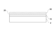
- 3 is a drawing schematically showing a process of forming a conductive film.
- 3 is a drawing schematically showing a process of forming a conductive film.
- 3 is a drawing schematically showing a process of forming a conductive film. This is an AFM photograph of the surface of the substrate. This is an AFM photograph of the surface of the substrate.
- the configuration of the display panel 1 as one embodiment will be explained first, and then the details of one embodiment of the method for manufacturing the conductive film included in the display panel 1 will be explained. Then, a verification and evaluation experiment was conducted to confirm the effects of the present invention using an example of the method for manufacturing a conductive film of the present invention, and finally, the details of the verification and evaluation experiment will be explained.
- FIG. 1 is a schematic diagram showing the overall configuration of one embodiment of a display panel 1. As shown in FIG. The display panel 1 has a base material 2, and one surface of the base material 2 is provided with an element region 2a and a peripheral region 2b.
- the base material 2 is formed of a material having translucency, and specifically includes, for example, a glass substrate, a quartz substrate, or an organic resin substrate.
- the material for the organic resin substrate include polyimide.
- the organic resin substrate can have a thickness ranging from several micrometers to several tens of micrometers, making it possible to realize a flexible sheet display.
- the element area 2a is an area where elements for displaying images are formed.
- a lower layer electrode is provided, and an insulating layer is provided on the lower layer electrode.
- An organic resin layer is provided on the insulating layer, and a conductive film is provided on the organic resin layer.
- the material of the organic resin layer is an organic material containing a polymer having hydrocarbon groups.
- the material of the conductive film is CNT.
- As the type of CNT single-walled carbon nanotubes or multi-walled carbon nanotubes having two or more layers can be employed, and single-walled carbon nanotubes are preferable.
- a conductive film made of carbon nanotubes has a transmittance that varies depending on the film thickness, but is a transparent conductive film that is transparent to visible light.
- the material constituting the organic resin layer is an organic resin material containing a polymer having a hydrocarbon group.
- examples of the material constituting the organic resin layer include polyimide resin, polyamide resin, polyether resin, polyester resin, and the like.
- the material constituting the organic resin layer is preferably a material containing an aromatic hydrocarbon, and more preferably a material containing a polycyclic aromatic hydrocarbon.
- the coating film is formed by applying a dispersion liquid containing carbon nanotubes and a dispersant.
- the dispersant is not particularly limited, it is preferable to use a polyamic acid having a structural moiety represented by formula (1) in terms of improving the dispersibility of carbon nanotubes. Just to be sure, equation (1) is reproduced.
- R 1 is a tetravalent organic group that constitutes a tetracarboxylic acid
- R 2 is a divalent organic group that constitutes a diamine
- n represents a positive integer.
- tetravalent organic group constituting the tetracarboxylic acid represented by R1 include pyromellitic acid, 2,3,6,7-naphthalenetetracarboxylic acid, and 1,2,5,6-naphthalenetetracarboxylic acid.
- Carboxylic acid 1,4,5,8-naphthalenetetracarboxylic acid, 2,3,6,7-anthracenetetracarboxylic acid, 1,2,5,6-anthracenetetracarboxylic acid, 3,3',4,4 '-Biphenyltetracarboxylic acid, 2,3,3',4-biphenyltetracarboxylic acid, bis(3,4-dicarboxyphenyl) ether, 3,3'4,4'-benzophenonetetracarboxylic acid, bis(3 ,4-dicarboxyphenyl) sulfone, bis(3,4-dicarboxyphenyl)methane, 2,2-bis(3,4-dicarboxyphenyl)propane, 1,1,1,3,3,3-hexane Fluoro-2,2-bis(3,4-dicarboxyphenyl)propane, bis(3,4-dicarboxyphenyl)dimethylsilane, bis(3,4-dica
- divalent organic group constituting the diamine represented by R2 include p-phenylenediamine, m-phenylenediamine, 2,5-diaminotoluene, 2,6-diaminotoluene, 4,4'-diamino Biphenyl, 3,3'-dimethyl-4,4'-diaminobiphenyl, 3,3'-dimethoxy-4,4'-diaminobiphenyl, diaminodiphenylmethane, diaminodiphenyl ether, 2,2'-diaminodiphenylpropane, bis(3 ,5-diethyl-4-aminophenyl)methane, diaminodiphenylsulfone, diaminobenzophenone, diaminonaphthalene, 1,4-bis(4-aminophenoxy)benzene, 1,4-bis(4-aminophenyl)benzene, 9, 10-bis(
- R 1 in the above formula (1) is a cyclobutane ring.
- the ring structure decomposes and a structural change of the polyamic acid occurs, thereby making it possible to remove the dispersant. This is preferable in that it can be easily removed.
- the above-mentioned dispersion liquid may contain an organic solvent as a dispersion medium.
- FIGS. 2 to 4. are drawings schematically showing the process of forming a conductive film. Note that in the method for manufacturing a conductive film of this embodiment, a conductive film is manufactured on an insulating layer formed on a substrate.
- a dispersion containing CNTs is applied onto the organic resin layer 20 to form a pattern of a coating film 30 (corresponding to step (B)). Note that in FIG. 3, for convenience, the coating film 30 is illustrated as being formed over the entire surface of the organic resin layer 20.
- a pattern is formed by a coating film of a dispersion containing CNTs on the organic resin layer 20 using printing techniques such as casting, screen printing, and inkjet.
- the solvent contained in the coating film is removed by drying, and the CNTs are fixed on the organic resin layer 20 to form a conductive film 40 (corresponding to step (C)).
- the conductive film 40 is illustrated as being formed over the entire surface of the organic resin layer 20, but the pattern of the conductive film 40 may be adjusted as appropriate.
- a dispersant extract is applied onto the conductive film formed on the substrate, and the dispersant is removed from the pattern formed by the coated film (corresponding to step (D)).
- a dispersion liquid is applied to the entire organic resin layer formed on the substrate, and then dried and washed. After this, it is also possible to separately form a photosensitive resist layer for patterning on the conductive film. In this case, after forming the photosensitive resist layer, the conductive layer is removed by etching, and the remaining photosensitive resist layer is removed.
- the combination of the dispersant and the dispersant extract is arbitrary, but the dispersant is an alkali-soluble polymer having a functional group that improves solubility in an alkaline aqueous solution, and the dispersant extract is an alkaline aqueous solution. is preferred.
- an alkaline aqueous solution as a dispersant extract, it becomes possible to selectively leave CNTs that are difficult to disperse in an alkaline aqueous solution on the organic resin layer.
- the polyamic acid structure of the dispersant may include a site such as cyclobutane that can be decomposed by light or heat to change the entire structure of the polyamic acid.
- the dispersant may contain an acid-dissociable group.
- An acid-dissociable group is a group that generates an acidic group such as a carboxyl group or a phenolic hydroxyl group by the action of an acid.
- the content of the dispersant relative to the CNTs is preferably within the range of 1,000% by mass to 100,000% by mass.
- the content of the dispersant for the CNTs is within this range, non-uniformity of the solvent in the drying process is prevented, and aggregation and localization of the CNTs due to drying is suppressed.
- the slit die coating method or the inkjet method is preferable from the viewpoint of uniformity of the coating film thickness and liquid saving. Further, from the viewpoint that electrode patterning can be performed only by coating, the inkjet method is more preferable.
- the CNTs contained in the coating film exhibit high adhesion to the organic resin layer, localization due to aggregation of the solvent in the drying process is suppressed. Furthermore, even in the solution immersion step for removing the dispersant, peeling and aggregation of CNTs do not occur, and localization of CNTs is suppressed. Therefore, even if a wiring with a very narrow pattern width is formed, locally high resistance parts and disconnections are less likely to occur.
- the organic resin layer can be formed by using the radiation-sensitive composition for forming the organic resin layer through the steps shown below.
- the organic resin layer formed by this formation method exhibits unique electrical properties, has excellent adhesion to CNTs, and has good chemical resistance and flatness. Further, according to the formation method, since heating is performed at 140° C. or lower, thermal deterioration of the substrate and elements provided on the substrate is suppressed. Each step will be explained in detail below.
- the radiation used at this time examples include ultraviolet rays, deep ultraviolet rays, X-rays, and charged particle beams.
- the mask used may be a multi-tone mask such as a halftone mask or a graytone mask.
- Synthesis of polymer [Synthesis example 1: Synthesis of polyamic acid] A polyamic acid having a hydrocarbon group in its side chain (hereinafter referred to as "polymer (paa-1)”) was obtained by the synthesis method described in Patent Document 2 above.
- FIG. 5 and 6 are both photographs taken using AFM of the surface of the substrate.
- FIG. 5 is an example of a photograph of the substrate surface where the unevenness of CNTs is observed
- FIG. This is an example of a photograph of a substrate surface that is not observed by AFM, that is, CNTs are covered with a resin/dispersant. If the dispersant on the surface has been removed and CNTs (carbon nanotubes) are exposed as shown in Figure 5, it is rated as “Good (A)”, and as shown in Figure 6, CNTs are partially exposed. A sample was rated as “fair (B)", and a sample where the surface was covered with resin and no exposed CNTs were observed, or the film formation was poor and could not be determined was graded as "poor (C)".
Landscapes
- Life Sciences & Earth Sciences (AREA)
- Engineering & Computer Science (AREA)
- Wood Science & Technology (AREA)
- Chemical & Material Sciences (AREA)
- Chemical Kinetics & Catalysis (AREA)
- General Chemical & Material Sciences (AREA)
- Carbon And Carbon Compounds (AREA)
- Manufacturing Of Electric Cables (AREA)
- Position Input By Displaying (AREA)
Priority Applications (1)
| Application Number | Priority Date | Filing Date | Title |
|---|---|---|---|
| JP2024526281A JPWO2023238530A1 (https=) | 2022-06-09 | 2023-04-24 |
Applications Claiming Priority (2)
| Application Number | Priority Date | Filing Date | Title |
|---|---|---|---|
| JP2022-093442 | 2022-06-09 | ||
| JP2022093442 | 2022-06-09 |
Publications (1)
| Publication Number | Publication Date |
|---|---|
| WO2023238530A1 true WO2023238530A1 (ja) | 2023-12-14 |
Family
ID=89118047
Family Applications (1)
| Application Number | Title | Priority Date | Filing Date |
|---|---|---|---|
| PCT/JP2023/016108 Ceased WO2023238530A1 (ja) | 2022-06-09 | 2023-04-24 | 導電膜の製造方法、タッチパネル、ディスプレイパネル |
Country Status (3)
| Country | Link |
|---|---|
| JP (1) | JPWO2023238530A1 (https=) |
| TW (1) | TW202348547A (https=) |
| WO (1) | WO2023238530A1 (https=) |
Citations (6)
| Publication number | Priority date | Publication date | Assignee | Title |
|---|---|---|---|---|
| JP2008177143A (ja) * | 2006-03-28 | 2008-07-31 | Toray Ind Inc | 透明導電性フィルム、その製造方法および導電性部材 |
| JP2008200613A (ja) * | 2007-02-20 | 2008-09-04 | Toray Ind Inc | カーボンナノチューブコーティング膜およびその製造方法 |
| JP2010202729A (ja) * | 2009-03-02 | 2010-09-16 | Hitachi Chemical Dupont Microsystems Ltd | フレキシブルデバイス基板用ポリイミド前駆体樹脂組成物及びそれを用いたフレキシブルデバイスの製造方法、フレキシブルデバイス |
| JP2010214837A (ja) * | 2009-03-18 | 2010-09-30 | Toray Ind Inc | 透明導電膜付き基材の製造方法 |
| JP2020090626A (ja) * | 2018-12-06 | 2020-06-11 | 株式会社マルアイ | Rfid用インキ組成物とそれを用いたrfidの導電性パターンの製造方法 |
| WO2021033482A1 (ja) * | 2019-08-19 | 2021-02-25 | Jsr株式会社 | 分散組成物、分散剤、異方性膜及びその製造方法、並びに異方性膜形成装置 |
-
2023
- 2023-04-24 JP JP2024526281A patent/JPWO2023238530A1/ja active Pending
- 2023-04-24 WO PCT/JP2023/016108 patent/WO2023238530A1/ja not_active Ceased
- 2023-05-15 TW TW112117859A patent/TW202348547A/zh unknown
Patent Citations (6)
| Publication number | Priority date | Publication date | Assignee | Title |
|---|---|---|---|---|
| JP2008177143A (ja) * | 2006-03-28 | 2008-07-31 | Toray Ind Inc | 透明導電性フィルム、その製造方法および導電性部材 |
| JP2008200613A (ja) * | 2007-02-20 | 2008-09-04 | Toray Ind Inc | カーボンナノチューブコーティング膜およびその製造方法 |
| JP2010202729A (ja) * | 2009-03-02 | 2010-09-16 | Hitachi Chemical Dupont Microsystems Ltd | フレキシブルデバイス基板用ポリイミド前駆体樹脂組成物及びそれを用いたフレキシブルデバイスの製造方法、フレキシブルデバイス |
| JP2010214837A (ja) * | 2009-03-18 | 2010-09-30 | Toray Ind Inc | 透明導電膜付き基材の製造方法 |
| JP2020090626A (ja) * | 2018-12-06 | 2020-06-11 | 株式会社マルアイ | Rfid用インキ組成物とそれを用いたrfidの導電性パターンの製造方法 |
| WO2021033482A1 (ja) * | 2019-08-19 | 2021-02-25 | Jsr株式会社 | 分散組成物、分散剤、異方性膜及びその製造方法、並びに異方性膜形成装置 |
Also Published As
| Publication number | Publication date |
|---|---|
| JPWO2023238530A1 (https=) | 2023-12-14 |
| TW202348547A (zh) | 2023-12-16 |
Similar Documents
| Publication | Publication Date | Title |
|---|---|---|
| TW574317B (en) | Polyamic acid resin composition | |
| EP2902846B1 (en) | Positive photosensitive resin composition | |
| JP2007183388A (ja) | 感光性樹脂組成物、耐熱性樹脂パターンの製造方法および有機電界発光素子 | |
| JP2023177343A (ja) | 感光性組成物及びその製造方法、硬化物及びその製造方法、表示素子並びにポリイミド | |
| TWI901750B (zh) | 正型感光性樹脂組成物 | |
| WO2024048270A1 (ja) | 導電膜の製造方法、分散液、感放射線性樹脂組成物、発光素子 | |
| CN112180684B (zh) | 正型感光性树脂组合物、固化膜及其图案加工方法 | |
| JP2024082310A (ja) | 導電膜の製造方法、タッチパネル、ディスプレイパネル | |
| JP2006021491A (ja) | 積層構造体、積層構造体を用いた光学素子、表示素子、演算素子及びこれらの製造方法 | |
| WO2023238530A1 (ja) | 導電膜の製造方法、タッチパネル、ディスプレイパネル | |
| JP2009192760A (ja) | ポジ型感光性樹脂組成物 | |
| JP3813060B2 (ja) | ナフトール構造を有するイオン形光酸発生剤及びこれを用いた感光性ポリイミド組成物 | |
| WO2024171805A1 (ja) | ポリイミド樹脂、感光性樹脂組成物、硬化物、有機el表示装置、および電子部品 | |
| WO2025057653A1 (ja) | 導電膜の製造方法、タッチパネル、ディスプレイパネル | |
| KR101113037B1 (ko) | 포지티브형 감광성 수지 조성물 | |
| KR101392167B1 (ko) | 포지티브형 감광성 폴리이미드 바니쉬 조성물, 포지티브형 폴리이미드 및 이를 포함하는 필름 | |
| JP2025522256A (ja) | 縦型有機発光トランジスタ素子の製造方法、表示装置 | |
| JP3319000B2 (ja) | 化学線感応性組成物 | |
| CN100492173C (zh) | 正型感光性的聚酰亚胺的涂料组合物 | |
| JP2002122993A (ja) | 感光性樹脂組成物およびポジ型パターン形成方法 | |
| CN105452383A (zh) | 感光性树脂组合物、其浮雕图案膜、浮雕图案膜的制造方法、包含浮雕图案膜的电子部件或光学制品、和包含感光性树脂组合物的粘接剂 | |
| JP2004020667A (ja) | 感光性樹脂組成物およびポジ型パターン形成方法 | |
| JP2011173429A (ja) | 積層構造体 | |
| JP2006350262A (ja) | ポジ型感光性ポリイミド組成物及びそれを用いたポリイミドパターンの形成方法 | |
| KR101421789B1 (ko) | 패턴의 제조방법 |
Legal Events
| Date | Code | Title | Description |
|---|---|---|---|
| 121 | Ep: the epo has been informed by wipo that ep was designated in this application |
Ref document number: 23819517 Country of ref document: EP Kind code of ref document: A1 |
|
| WWE | Wipo information: entry into national phase |
Ref document number: 2024526281 Country of ref document: JP |
|
| NENP | Non-entry into the national phase |
Ref country code: DE |
|
| 122 | Ep: pct application non-entry in european phase |
Ref document number: 23819517 Country of ref document: EP Kind code of ref document: A1 |