WO2023238530A1 - Method for producing electroconductive film, touch panel, display panel - Google Patents
Method for producing electroconductive film, touch panel, display panel Download PDFInfo
- Publication number
- WO2023238530A1 WO2023238530A1 PCT/JP2023/016108 JP2023016108W WO2023238530A1 WO 2023238530 A1 WO2023238530 A1 WO 2023238530A1 JP 2023016108 W JP2023016108 W JP 2023016108W WO 2023238530 A1 WO2023238530 A1 WO 2023238530A1
- Authority
- WO
- WIPO (PCT)
- Prior art keywords
- dispersant
- conductive film
- organic resin
- resin layer
- manufacturing
- Prior art date
Links
- 238000004519 manufacturing process Methods 0.000 title claims abstract description 38
- 239000012789 electroconductive film Substances 0.000 title abstract 3
- 239000002041 carbon nanotube Substances 0.000 claims abstract description 63
- 239000002270 dispersing agent Substances 0.000 claims abstract description 55
- 239000011347 resin Substances 0.000 claims abstract description 53
- 229920005989 resin Polymers 0.000 claims abstract description 53
- 238000000034 method Methods 0.000 claims abstract description 52
- 238000000576 coating method Methods 0.000 claims abstract description 48
- 239000011248 coating agent Substances 0.000 claims abstract description 44
- 239000006185 dispersion Substances 0.000 claims abstract description 42
- 239000000463 material Substances 0.000 claims abstract description 40
- OKTJSMMVPCPJKN-UHFFFAOYSA-N Carbon Chemical compound [C] OKTJSMMVPCPJKN-UHFFFAOYSA-N 0.000 claims abstract description 32
- 229910021393 carbon nanotube Inorganic materials 0.000 claims abstract description 25
- 229920000642 polymer Polymers 0.000 claims abstract description 25
- 239000007788 liquid Substances 0.000 claims abstract description 12
- 238000001035 drying Methods 0.000 claims abstract description 11
- 125000001183 hydrocarbyl group Chemical group 0.000 claims abstract 2
- 229920005575 poly(amic acid) Polymers 0.000 claims description 11
- 239000007864 aqueous solution Substances 0.000 claims description 9
- 125000002887 hydroxy group Chemical group [H]O* 0.000 claims description 5
- 239000003960 organic solvent Substances 0.000 claims description 4
- 150000004945 aromatic hydrocarbons Chemical class 0.000 claims description 3
- 125000003178 carboxy group Chemical group [H]OC(*)=O 0.000 claims description 3
- 125000000524 functional group Chemical group 0.000 claims description 3
- 238000007654 immersion Methods 0.000 claims description 3
- ISWSIDIOOBJBQZ-UHFFFAOYSA-N phenol group Chemical group C1(=CC=CC=C1)O ISWSIDIOOBJBQZ-UHFFFAOYSA-N 0.000 claims description 3
- 125000005575 polycyclic aromatic hydrocarbon group Chemical group 0.000 claims description 3
- 230000015572 biosynthetic process Effects 0.000 abstract description 24
- 239000003575 carbonaceous material Substances 0.000 abstract description 4
- 239000010408 film Substances 0.000 abstract 3
- 238000000605 extraction Methods 0.000 abstract 1
- 239000000203 mixture Substances 0.000 description 29
- 239000000758 substrate Substances 0.000 description 21
- SECXISVLQFMRJM-UHFFFAOYSA-N N-Methylpyrrolidone Chemical compound CN1CCCC1=O SECXISVLQFMRJM-UHFFFAOYSA-N 0.000 description 18
- 239000002109 single walled nanotube Substances 0.000 description 17
- 238000003786 synthesis reaction Methods 0.000 description 15
- 238000011156 evaluation Methods 0.000 description 14
- 239000002904 solvent Substances 0.000 description 14
- 230000005855 radiation Effects 0.000 description 13
- KWYUFKZDYYNOTN-UHFFFAOYSA-M Potassium hydroxide Chemical compound [OH-].[K+] KWYUFKZDYYNOTN-UHFFFAOYSA-M 0.000 description 9
- HEMHJVSKTPXQMS-UHFFFAOYSA-M Sodium hydroxide Chemical compound [OH-].[Na+] HEMHJVSKTPXQMS-UHFFFAOYSA-M 0.000 description 9
- WGTYBPLFGIVFAS-UHFFFAOYSA-M tetramethylammonium hydroxide Chemical compound [OH-].C[N+](C)(C)C WGTYBPLFGIVFAS-UHFFFAOYSA-M 0.000 description 8
- 239000004065 semiconductor Substances 0.000 description 7
- 238000001132 ultrasonic dispersion Methods 0.000 description 7
- 239000002253 acid Substances 0.000 description 6
- 238000004220 aggregation Methods 0.000 description 6
- 230000002776 aggregation Effects 0.000 description 6
- 150000004985 diamines Chemical class 0.000 description 6
- 238000010438 heat treatment Methods 0.000 description 6
- 150000002430 hydrocarbons Chemical group 0.000 description 6
- 125000000962 organic group Chemical group 0.000 description 6
- 239000000243 solution Substances 0.000 description 6
- -1 aromatic tetracarboxylic acids Chemical class 0.000 description 5
- 238000004528 spin coating Methods 0.000 description 5
- ATUOYWHBWRKTHZ-UHFFFAOYSA-N Propane Chemical compound CCC ATUOYWHBWRKTHZ-UHFFFAOYSA-N 0.000 description 4
- CDBYLPFSWZWCQE-UHFFFAOYSA-L Sodium Carbonate Chemical compound [Na+].[Na+].[O-]C([O-])=O CDBYLPFSWZWCQE-UHFFFAOYSA-L 0.000 description 4
- 150000001875 compounds Chemical class 0.000 description 4
- 125000006159 dianhydride group Chemical group 0.000 description 4
- 238000002474 experimental method Methods 0.000 description 4
- VNWKTOKETHGBQD-UHFFFAOYSA-N methane Chemical compound C VNWKTOKETHGBQD-UHFFFAOYSA-N 0.000 description 4
- 239000011368 organic material Substances 0.000 description 4
- 229920001721 polyimide Polymers 0.000 description 4
- 150000000000 tetracarboxylic acids Chemical class 0.000 description 4
- 238000012795 verification Methods 0.000 description 4
- CSCPPACGZOOCGX-UHFFFAOYSA-N Acetone Chemical compound CC(C)=O CSCPPACGZOOCGX-UHFFFAOYSA-N 0.000 description 3
- LFQSCWFLJHTTHZ-UHFFFAOYSA-N Ethanol Chemical compound CCO LFQSCWFLJHTTHZ-UHFFFAOYSA-N 0.000 description 3
- XEKOWRVHYACXOJ-UHFFFAOYSA-N Ethyl acetate Chemical compound CCOC(C)=O XEKOWRVHYACXOJ-UHFFFAOYSA-N 0.000 description 3
- KFZMGEQAYNKOFK-UHFFFAOYSA-N Isopropanol Chemical compound CC(C)O KFZMGEQAYNKOFK-UHFFFAOYSA-N 0.000 description 3
- 239000004642 Polyimide Substances 0.000 description 3
- 125000001995 cyclobutyl group Chemical group [H]C1([H])C([H])([H])C([H])(*)C1([H])[H] 0.000 description 3
- 238000007607 die coating method Methods 0.000 description 3
- 238000007598 dipping method Methods 0.000 description 3
- 239000011521 glass Substances 0.000 description 3
- 230000004807 localization Effects 0.000 description 3
- 229910052751 metal Inorganic materials 0.000 description 3
- 239000002184 metal Substances 0.000 description 3
- 229910021392 nanocarbon Inorganic materials 0.000 description 3
- 239000012670 alkaline solution Substances 0.000 description 2
- 238000007611 bar coating method Methods 0.000 description 2
- 230000000052 comparative effect Effects 0.000 description 2
- 238000011161 development Methods 0.000 description 2
- 238000010586 diagram Methods 0.000 description 2
- KZTYYGOKRVBIMI-UHFFFAOYSA-N diphenyl sulfone Chemical compound C=1C=CC=CC=1S(=O)(=O)C1=CC=CC=C1 KZTYYGOKRVBIMI-UHFFFAOYSA-N 0.000 description 2
- 230000000694 effects Effects 0.000 description 2
- 229910044991 metal oxide Inorganic materials 0.000 description 2
- 150000004706 metal oxides Chemical class 0.000 description 2
- 150000002739 metals Chemical class 0.000 description 2
- 239000002048 multi walled nanotube Substances 0.000 description 2
- 239000002245 particle Substances 0.000 description 2
- 238000000059 patterning Methods 0.000 description 2
- 230000002093 peripheral effect Effects 0.000 description 2
- 125000001997 phenyl group Chemical group [H]C1=C([H])C([H])=C(*)C([H])=C1[H] 0.000 description 2
- 238000002360 preparation method Methods 0.000 description 2
- 238000007639 printing Methods 0.000 description 2
- 239000001294 propane Substances 0.000 description 2
- CYIDZMCFTVVTJO-UHFFFAOYSA-N pyromellitic acid Chemical compound OC(=O)C1=CC(C(O)=O)=C(C(O)=O)C=C1C(O)=O CYIDZMCFTVVTJO-UHFFFAOYSA-N 0.000 description 2
- 238000004062 sedimentation Methods 0.000 description 2
- 229910000029 sodium carbonate Inorganic materials 0.000 description 2
- 238000005507 spraying Methods 0.000 description 2
- 239000000126 substance Substances 0.000 description 2
- 238000001308 synthesis method Methods 0.000 description 2
- XFNJVJPLKCPIBV-UHFFFAOYSA-N trimethylenediamine Chemical compound NCCCN XFNJVJPLKCPIBV-UHFFFAOYSA-N 0.000 description 2
- FHBXQJDYHHJCIF-UHFFFAOYSA-N (2,3-diaminophenyl)-phenylmethanone Chemical compound NC1=CC=CC(C(=O)C=2C=CC=CC=2)=C1N FHBXQJDYHHJCIF-UHFFFAOYSA-N 0.000 description 1
- WZCQRUWWHSTZEM-UHFFFAOYSA-N 1,3-phenylenediamine Chemical compound NC1=CC=CC(N)=C1 WZCQRUWWHSTZEM-UHFFFAOYSA-N 0.000 description 1
- CBCKQZAAMUWICA-UHFFFAOYSA-N 1,4-phenylenediamine Chemical compound NC1=CC=C(N)C=C1 CBCKQZAAMUWICA-UHFFFAOYSA-N 0.000 description 1
- 229940075142 2,5-diaminotoluene Drugs 0.000 description 1
- RLYCRLGLCUXUPO-UHFFFAOYSA-N 2,6-diaminotoluene Chemical compound CC1=C(N)C=CC=C1N RLYCRLGLCUXUPO-UHFFFAOYSA-N 0.000 description 1
- PAYVNGLXRRKQEG-UHFFFAOYSA-N 2-(1,2,3,4-tetrahydronaphthalen-1-yl)butanedioic acid Chemical compound C1=CC=C2C(C(CC(=O)O)C(O)=O)CCCC2=C1 PAYVNGLXRRKQEG-UHFFFAOYSA-N 0.000 description 1
- RLHGFJMGWQXPBW-UHFFFAOYSA-N 2-hydroxy-3-(1h-imidazol-5-ylmethyl)benzamide Chemical compound NC(=O)C1=CC=CC(CC=2NC=NC=2)=C1O RLHGFJMGWQXPBW-UHFFFAOYSA-N 0.000 description 1
- OBCSAIDCZQSFQH-UHFFFAOYSA-N 2-methyl-1,4-phenylenediamine Chemical compound CC1=CC(N)=CC=C1N OBCSAIDCZQSFQH-UHFFFAOYSA-N 0.000 description 1
- JRBJSXQPQWSCCF-UHFFFAOYSA-N 3,3'-Dimethoxybenzidine Chemical group C1=C(N)C(OC)=CC(C=2C=C(OC)C(N)=CC=2)=C1 JRBJSXQPQWSCCF-UHFFFAOYSA-N 0.000 description 1
- NUIURNJTPRWVAP-UHFFFAOYSA-N 3,3'-Dimethylbenzidine Chemical group C1=C(N)C(C)=CC(C=2C=C(C)C(N)=CC=2)=C1 NUIURNJTPRWVAP-UHFFFAOYSA-N 0.000 description 1
- UENRXLSRMCSUSN-UHFFFAOYSA-M 3,5-diaminobenzoate Chemical compound NC1=CC(N)=CC(C([O-])=O)=C1 UENRXLSRMCSUSN-UHFFFAOYSA-M 0.000 description 1
- RHRNYXVSZLSRRP-UHFFFAOYSA-N 3-(carboxymethyl)cyclopentane-1,2,4-tricarboxylic acid Chemical compound OC(=O)CC1C(C(O)=O)CC(C(O)=O)C1C(O)=O RHRNYXVSZLSRRP-UHFFFAOYSA-N 0.000 description 1
- GPXCORHXFPYJEH-UHFFFAOYSA-N 3-[[3-aminopropyl(dimethyl)silyl]oxy-dimethylsilyl]propan-1-amine Chemical compound NCCC[Si](C)(C)O[Si](C)(C)CCCN GPXCORHXFPYJEH-UHFFFAOYSA-N 0.000 description 1
- AIVVXPSKEVWKMY-UHFFFAOYSA-N 4-(3,4-dicarboxyphenoxy)phthalic acid Chemical compound C1=C(C(O)=O)C(C(=O)O)=CC=C1OC1=CC=C(C(O)=O)C(C(O)=O)=C1 AIVVXPSKEVWKMY-UHFFFAOYSA-N 0.000 description 1
- LFBALUPVVFCEPA-UHFFFAOYSA-N 4-(3,4-dicarboxyphenyl)phthalic acid Chemical compound C1=C(C(O)=O)C(C(=O)O)=CC=C1C1=CC=C(C(O)=O)C(C(O)=O)=C1 LFBALUPVVFCEPA-UHFFFAOYSA-N 0.000 description 1
- AVCOFPOLGHKJQB-UHFFFAOYSA-N 4-(3,4-dicarboxyphenyl)sulfonylphthalic acid Chemical compound C1=C(C(O)=O)C(C(=O)O)=CC=C1S(=O)(=O)C1=CC=C(C(O)=O)C(C(O)=O)=C1 AVCOFPOLGHKJQB-UHFFFAOYSA-N 0.000 description 1
- XDYLWBWPEDSSLU-UHFFFAOYSA-N 4-(3-carboxyphenyl)benzene-1,2,3-tricarboxylic acid Chemical compound OC(=O)C1=CC=CC(C=2C(=C(C(O)=O)C(C(O)=O)=CC=2)C(O)=O)=C1 XDYLWBWPEDSSLU-UHFFFAOYSA-N 0.000 description 1
- HLBLWEWZXPIGSM-UHFFFAOYSA-N 4-Aminophenyl ether Chemical compound C1=CC(N)=CC=C1OC1=CC=C(N)C=C1 HLBLWEWZXPIGSM-UHFFFAOYSA-N 0.000 description 1
- HNHQPIBXQALMMN-UHFFFAOYSA-N 4-[(3,4-dicarboxyphenyl)-dimethylsilyl]phthalic acid Chemical compound C=1C=C(C(O)=O)C(C(O)=O)=CC=1[Si](C)(C)C1=CC=C(C(O)=O)C(C(O)=O)=C1 HNHQPIBXQALMMN-UHFFFAOYSA-N 0.000 description 1
- MOCQGMXEHQTAEN-UHFFFAOYSA-N 4-[(3,4-dicarboxyphenyl)-diphenylsilyl]phthalic acid Chemical compound C1=C(C(O)=O)C(C(=O)O)=CC=C1[Si](C=1C=C(C(C(O)=O)=CC=1)C(O)=O)(C=1C=CC=CC=1)C1=CC=CC=C1 MOCQGMXEHQTAEN-UHFFFAOYSA-N 0.000 description 1
- IWXCYYWDGDDPAC-UHFFFAOYSA-N 4-[(3,4-dicarboxyphenyl)methyl]phthalic acid Chemical compound C1=C(C(O)=O)C(C(=O)O)=CC=C1CC1=CC=C(C(O)=O)C(C(O)=O)=C1 IWXCYYWDGDDPAC-UHFFFAOYSA-N 0.000 description 1
- IGSBHTZEJMPDSZ-UHFFFAOYSA-N 4-[(4-amino-3-methylcyclohexyl)methyl]-2-methylcyclohexan-1-amine Chemical compound C1CC(N)C(C)CC1CC1CC(C)C(N)CC1 IGSBHTZEJMPDSZ-UHFFFAOYSA-N 0.000 description 1
- ASNOFHCTUSIHOM-UHFFFAOYSA-N 4-[10-(4-aminophenyl)anthracen-9-yl]aniline Chemical compound C1=CC(N)=CC=C1C(C1=CC=CC=C11)=C(C=CC=C2)C2=C1C1=CC=C(N)C=C1 ASNOFHCTUSIHOM-UHFFFAOYSA-N 0.000 description 1
- AZSDTRIPJLXNKU-UHFFFAOYSA-N 4-[2-(3,4-dicarboxyphenyl)-1-fluoropropan-2-yl]phthalic acid Chemical compound C(=O)(O)C=1C=C(C=CC=1C(=O)O)C(CF)(C)C1=CC(=C(C=C1)C(=O)O)C(=O)O AZSDTRIPJLXNKU-UHFFFAOYSA-N 0.000 description 1
- GEYAGBVEAJGCFB-UHFFFAOYSA-N 4-[2-(3,4-dicarboxyphenyl)propan-2-yl]phthalic acid Chemical compound C=1C=C(C(O)=O)C(C(O)=O)=CC=1C(C)(C)C1=CC=C(C(O)=O)C(C(O)=O)=C1 GEYAGBVEAJGCFB-UHFFFAOYSA-N 0.000 description 1
- BEKFRNOZJSYWKZ-UHFFFAOYSA-N 4-[2-(4-aminophenyl)-1,1,1,3,3,3-hexafluoropropan-2-yl]aniline Chemical compound C1=CC(N)=CC=C1C(C(F)(F)F)(C(F)(F)F)C1=CC=C(N)C=C1 BEKFRNOZJSYWKZ-UHFFFAOYSA-N 0.000 description 1
- WUPRYUDHUFLKFL-UHFFFAOYSA-N 4-[3-(4-aminophenoxy)phenoxy]aniline Chemical compound C1=CC(N)=CC=C1OC1=CC=CC(OC=2C=CC(N)=CC=2)=C1 WUPRYUDHUFLKFL-UHFFFAOYSA-N 0.000 description 1
- JCRRFJIVUPSNTA-UHFFFAOYSA-N 4-[4-(4-aminophenoxy)phenoxy]aniline Chemical compound C1=CC(N)=CC=C1OC(C=C1)=CC=C1OC1=CC=C(N)C=C1 JCRRFJIVUPSNTA-UHFFFAOYSA-N 0.000 description 1
- QBSMHWVGUPQNJJ-UHFFFAOYSA-N 4-[4-(4-aminophenyl)phenyl]aniline Chemical compound C1=CC(N)=CC=C1C1=CC=C(C=2C=CC(N)=CC=2)C=C1 QBSMHWVGUPQNJJ-UHFFFAOYSA-N 0.000 description 1
- HHLMWQDRYZAENA-UHFFFAOYSA-N 4-[4-[2-[4-(4-aminophenoxy)phenyl]-1,1,1,3,3,3-hexafluoropropan-2-yl]phenoxy]aniline Chemical compound C1=CC(N)=CC=C1OC1=CC=C(C(C=2C=CC(OC=3C=CC(N)=CC=3)=CC=2)(C(F)(F)F)C(F)(F)F)C=C1 HHLMWQDRYZAENA-UHFFFAOYSA-N 0.000 description 1
- UURATDYSEHCBAO-UHFFFAOYSA-N 4-[6-(3,4-dicarboxyphenyl)pyridin-2-yl]phthalic acid Chemical compound C1=C(C(O)=O)C(C(=O)O)=CC=C1C1=CC=CC(C=2C=C(C(C(O)=O)=CC=2)C(O)=O)=N1 UURATDYSEHCBAO-UHFFFAOYSA-N 0.000 description 1
- DKPFZGUDAPQIHT-UHFFFAOYSA-N Butyl acetate Natural products CCCCOC(C)=O DKPFZGUDAPQIHT-UHFFFAOYSA-N 0.000 description 1
- RYGMFSIKBFXOCR-UHFFFAOYSA-N Copper Chemical compound [Cu] RYGMFSIKBFXOCR-UHFFFAOYSA-N 0.000 description 1
- PMPVIKIVABFJJI-UHFFFAOYSA-N Cyclobutane Chemical compound C1CCC1 PMPVIKIVABFJJI-UHFFFAOYSA-N 0.000 description 1
- ZPAKUZKMGJJMAA-UHFFFAOYSA-N Cyclohexane-1,2,4,5-tetracarboxylic acid Chemical compound OC(=O)C1CC(C(O)=O)C(C(O)=O)CC1C(O)=O ZPAKUZKMGJJMAA-UHFFFAOYSA-N 0.000 description 1
- MQJKPEGWNLWLTK-UHFFFAOYSA-N Dapsone Chemical compound C1=CC(N)=CC=C1S(=O)(=O)C1=CC=C(N)C=C1 MQJKPEGWNLWLTK-UHFFFAOYSA-N 0.000 description 1
- PIICEJLVQHRZGT-UHFFFAOYSA-N Ethylenediamine Chemical compound NCCN PIICEJLVQHRZGT-UHFFFAOYSA-N 0.000 description 1
- 101150033824 PAA1 gene Proteins 0.000 description 1
- 239000004721 Polyphenylene oxide Substances 0.000 description 1
- GSEJCLTVZPLZKY-UHFFFAOYSA-N Triethanolamine Chemical compound OCCN(CCO)CCO GSEJCLTVZPLZKY-UHFFFAOYSA-N 0.000 description 1
- 125000004036 acetal group Chemical group 0.000 description 1
- 230000002378 acidificating effect Effects 0.000 description 1
- 125000002723 alicyclic group Chemical group 0.000 description 1
- 229910052782 aluminium Inorganic materials 0.000 description 1
- XAGFODPZIPBFFR-UHFFFAOYSA-N aluminium Chemical compound [Al] XAGFODPZIPBFFR-UHFFFAOYSA-N 0.000 description 1
- BALIDSJNGIOVDT-UHFFFAOYSA-N anthracene-1,2,5,6-tetracarboxylic acid Chemical compound OC(=O)C1=C(C(O)=O)C=CC2=CC3=C(C(O)=O)C(C(=O)O)=CC=C3C=C21 BALIDSJNGIOVDT-UHFFFAOYSA-N 0.000 description 1
- MRSWDOKCESOYBI-UHFFFAOYSA-N anthracene-2,3,6,7-tetracarboxylic acid Chemical compound OC(=O)C1=C(C(O)=O)C=C2C=C(C=C(C(C(=O)O)=C3)C(O)=O)C3=CC2=C1 MRSWDOKCESOYBI-UHFFFAOYSA-N 0.000 description 1
- HFACYLZERDEVSX-UHFFFAOYSA-N benzidine Chemical group C1=CC(N)=CC=C1C1=CC=C(N)C=C1 HFACYLZERDEVSX-UHFFFAOYSA-N 0.000 description 1
- 150000001732 carboxylic acid derivatives Chemical class 0.000 description 1
- 238000005266 casting Methods 0.000 description 1
- 239000003795 chemical substances by application Substances 0.000 description 1
- 239000000470 constituent Substances 0.000 description 1
- 229910052802 copper Inorganic materials 0.000 description 1
- 239000010949 copper Substances 0.000 description 1
- CURBACXRQKTCKZ-UHFFFAOYSA-N cyclobutane-1,2,3,4-tetracarboxylic acid Chemical compound OC(=O)C1C(C(O)=O)C(C(O)=O)C1C(O)=O CURBACXRQKTCKZ-UHFFFAOYSA-N 0.000 description 1
- WOSVXXBNNCUXMT-UHFFFAOYSA-N cyclopentane-1,2,3,4-tetracarboxylic acid Chemical compound OC(=O)C1CC(C(O)=O)C(C(O)=O)C1C(O)=O WOSVXXBNNCUXMT-UHFFFAOYSA-N 0.000 description 1
- 238000000354 decomposition reaction Methods 0.000 description 1
- 230000006866 deterioration Effects 0.000 description 1
- 239000002612 dispersion medium Substances 0.000 description 1
- 238000010894 electron beam technology Methods 0.000 description 1
- 238000005516 engineering process Methods 0.000 description 1
- 238000005530 etching Methods 0.000 description 1
- 230000001747 exhibiting effect Effects 0.000 description 1
- VLKZOEOYAKHREP-UHFFFAOYSA-N hexane Substances CCCCCC VLKZOEOYAKHREP-UHFFFAOYSA-N 0.000 description 1
- NAQMVNRVTILPCV-UHFFFAOYSA-N hexane-1,6-diamine Chemical compound NCCCCCCN NAQMVNRVTILPCV-UHFFFAOYSA-N 0.000 description 1
- FUZZWVXGSFPDMH-UHFFFAOYSA-N hexanoic acid Chemical compound CCCCCC(O)=O FUZZWVXGSFPDMH-UHFFFAOYSA-N 0.000 description 1
- 230000001771 impaired effect Effects 0.000 description 1
- 229940018564 m-phenylenediamine Drugs 0.000 description 1
- OBKARQMATMRWQZ-UHFFFAOYSA-N naphthalene-1,2,5,6-tetracarboxylic acid Chemical compound OC(=O)C1=C(C(O)=O)C=CC2=C(C(O)=O)C(C(=O)O)=CC=C21 OBKARQMATMRWQZ-UHFFFAOYSA-N 0.000 description 1
- NTNWKDHZTDQSST-UHFFFAOYSA-N naphthalene-1,2-diamine Chemical compound C1=CC=CC2=C(N)C(N)=CC=C21 NTNWKDHZTDQSST-UHFFFAOYSA-N 0.000 description 1
- OLAPPGSPBNVTRF-UHFFFAOYSA-N naphthalene-1,4,5,8-tetracarboxylic acid Chemical compound C1=CC(C(O)=O)=C2C(C(=O)O)=CC=C(C(O)=O)C2=C1C(O)=O OLAPPGSPBNVTRF-UHFFFAOYSA-N 0.000 description 1
- DOBFTMLCEYUAQC-UHFFFAOYSA-N naphthalene-2,3,6,7-tetracarboxylic acid Chemical compound OC(=O)C1=C(C(O)=O)C=C2C=C(C(O)=O)C(C(=O)O)=CC2=C1 DOBFTMLCEYUAQC-UHFFFAOYSA-N 0.000 description 1
- 239000004745 nonwoven fabric Substances 0.000 description 1
- 230000003287 optical effect Effects 0.000 description 1
- 229920006122 polyamide resin Polymers 0.000 description 1
- 229920001225 polyester resin Polymers 0.000 description 1
- 239000004645 polyester resin Substances 0.000 description 1
- 229920000570 polyether Polymers 0.000 description 1
- 239000009719 polyimide resin Substances 0.000 description 1
- 229920001296 polysiloxane Polymers 0.000 description 1
- JREWFSHZWRKNBM-UHFFFAOYSA-N pyridine-2,3,4,5-tetracarboxylic acid Chemical compound OC(=O)C1=CN=C(C(O)=O)C(C(O)=O)=C1C(O)=O JREWFSHZWRKNBM-UHFFFAOYSA-N 0.000 description 1
- 239000010453 quartz Substances 0.000 description 1
- 238000007650 screen-printing Methods 0.000 description 1
- VYPSYNLAJGMNEJ-UHFFFAOYSA-N silicon dioxide Inorganic materials O=[Si]=O VYPSYNLAJGMNEJ-UHFFFAOYSA-N 0.000 description 1
- 239000007921 spray Substances 0.000 description 1
- 230000005469 synchrotron radiation Effects 0.000 description 1
- 229940073455 tetraethylammonium hydroxide Drugs 0.000 description 1
- LRGJRHZIDJQFCL-UHFFFAOYSA-M tetraethylazanium;hydroxide Chemical compound [OH-].CC[N+](CC)(CC)CC LRGJRHZIDJQFCL-UHFFFAOYSA-M 0.000 description 1
- 238000002834 transmittance Methods 0.000 description 1
- XLYOFNOQVPJJNP-UHFFFAOYSA-N water Substances O XLYOFNOQVPJJNP-UHFFFAOYSA-N 0.000 description 1
Images


Classifications
-
- B—PERFORMING OPERATIONS; TRANSPORTING
- B05—SPRAYING OR ATOMISING IN GENERAL; APPLYING FLUENT MATERIALS TO SURFACES, IN GENERAL
- B05D—PROCESSES FOR APPLYING FLUENT MATERIALS TO SURFACES, IN GENERAL
- B05D1/00—Processes for applying liquids or other fluent materials
- B05D1/36—Successively applying liquids or other fluent materials, e.g. without intermediate treatment
-
- B—PERFORMING OPERATIONS; TRANSPORTING
- B05—SPRAYING OR ATOMISING IN GENERAL; APPLYING FLUENT MATERIALS TO SURFACES, IN GENERAL
- B05D—PROCESSES FOR APPLYING FLUENT MATERIALS TO SURFACES, IN GENERAL
- B05D3/00—Pretreatment of surfaces to which liquids or other fluent materials are to be applied; After-treatment of applied coatings, e.g. intermediate treating of an applied coating preparatory to subsequent applications of liquids or other fluent materials
- B05D3/10—Pretreatment of surfaces to which liquids or other fluent materials are to be applied; After-treatment of applied coatings, e.g. intermediate treating of an applied coating preparatory to subsequent applications of liquids or other fluent materials by other chemical means
-
- B—PERFORMING OPERATIONS; TRANSPORTING
- B05—SPRAYING OR ATOMISING IN GENERAL; APPLYING FLUENT MATERIALS TO SURFACES, IN GENERAL
- B05D—PROCESSES FOR APPLYING FLUENT MATERIALS TO SURFACES, IN GENERAL
- B05D5/00—Processes for applying liquids or other fluent materials to surfaces to obtain special surface effects, finishes or structures
- B05D5/12—Processes for applying liquids or other fluent materials to surfaces to obtain special surface effects, finishes or structures to obtain a coating with specific electrical properties
-
- B—PERFORMING OPERATIONS; TRANSPORTING
- B05—SPRAYING OR ATOMISING IN GENERAL; APPLYING FLUENT MATERIALS TO SURFACES, IN GENERAL
- B05D—PROCESSES FOR APPLYING FLUENT MATERIALS TO SURFACES, IN GENERAL
- B05D7/00—Processes, other than flocking, specially adapted for applying liquids or other fluent materials to particular surfaces or for applying particular liquids or other fluent materials
- B05D7/24—Processes, other than flocking, specially adapted for applying liquids or other fluent materials to particular surfaces or for applying particular liquids or other fluent materials for applying particular liquids or other fluent materials
Definitions
- electrodes and wiring of semiconductor devices have often been formed of metals such as copper and aluminum.
- metals such as copper and aluminum.
- nanocarbon materials particularly carbon nanotubes (hereinafter sometimes abbreviated as "CNT")
- CNT carbon nanotubes
- conductive films made of nanocarbon materials can be formed into films that exhibit high transparency to visible light, there is a movement toward their active use in semiconductor optical devices.
- Patent Document 1 listed below describes a composition in which a solvent and CNTs are used as a composition with improved dispersibility of CNTs.
- Compositions containing the present invention are disclosed.
- the conductive film produced using the above composition has a problem in that it tends to aggregate during the drying process and the like, and its homogeneity tends to be impaired.
- a CNT transparent conductive film exhibits conductivity by forming a circuit through which current flows by folding fibrous CNTs like a nonwoven fabric. For this reason, unlike metal films and metal oxide films, it has been difficult to configure them to have stable characteristics, and it has been difficult to develop stable electrical characteristics.
- a conductive film when used in light emitting devices, touch panels, etc., it is required to form a conductive film as thin as possible in order to increase the transparency of visible light, and it is also required to form a conductive film with high conductivity and uniformity. be done. Even in such a case, a problem arises in that the conductive film is likely to be disconnected, similar to the above-mentioned semiconductor devices such as LSIs. More specifically, for example, when configuring wiring constituting a touch panel, wiring is formed with a width of 50 ⁇ m or less, or when creating a pixel electrode of a display panel, a lead line from a contact hole with a width of 50 ⁇ m or less is created. In some cases, wire breakage is particularly likely to occur.
- the method for manufacturing a conductive film of the present invention includes: a step (A) of applying an organic resin material containing a polymer having a hydrocarbon group onto a base material to form an organic resin layer; After carrying out the step (A), a step (B) of applying a dispersion liquid containing a dispersant and carbon nanotubes on the organic resin layer to form a coating film; After carrying out the step (B), a step (C) of drying the coating film; After carrying out the step (C), the method includes a step (D) of attaching a dispersant extract and removing the dispersant from the coating film.
- the step (D) may be a step of forming the coating film by immersing the base material in a dispersant extract.
- the dispersant is preferably a polymer having a constituent part represented by the following formula (1).
- the step (B) is a step of applying the dispersion liquid in which the content of the dispersant to the carbon material is within the range of 1,000% by mass to 100,000% by mass on the organic resin layer. I don't mind.
- the display panel of the present invention includes: A conductive film manufactured by the above manufacturing method is provided.
- a method for manufacturing a conductive film that has high conductivity and can evenly fix a conductive carbon material over the entire conductive film formation region.
- FIG. 1 is a schematic diagram showing the overall configuration of an embodiment of a display panel.
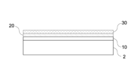
- 3 is a drawing schematically showing a process of forming a conductive film.
- 3 is a drawing schematically showing a process of forming a conductive film.
- 3 is a drawing schematically showing a process of forming a conductive film. This is an AFM photograph of the surface of the substrate. This is an AFM photograph of the surface of the substrate.
- the configuration of the display panel 1 as one embodiment will be explained first, and then the details of one embodiment of the method for manufacturing the conductive film included in the display panel 1 will be explained. Then, a verification and evaluation experiment was conducted to confirm the effects of the present invention using an example of the method for manufacturing a conductive film of the present invention, and finally, the details of the verification and evaluation experiment will be explained.
- FIG. 1 is a schematic diagram showing the overall configuration of one embodiment of a display panel 1. As shown in FIG. The display panel 1 has a base material 2, and one surface of the base material 2 is provided with an element region 2a and a peripheral region 2b.
- the base material 2 is formed of a material having translucency, and specifically includes, for example, a glass substrate, a quartz substrate, or an organic resin substrate.
- the material for the organic resin substrate include polyimide.
- the organic resin substrate can have a thickness ranging from several micrometers to several tens of micrometers, making it possible to realize a flexible sheet display.
- the element area 2a is an area where elements for displaying images are formed.
- a lower layer electrode is provided, and an insulating layer is provided on the lower layer electrode.
- An organic resin layer is provided on the insulating layer, and a conductive film is provided on the organic resin layer.
- the material of the organic resin layer is an organic material containing a polymer having hydrocarbon groups.
- the material of the conductive film is CNT.
- As the type of CNT single-walled carbon nanotubes or multi-walled carbon nanotubes having two or more layers can be employed, and single-walled carbon nanotubes are preferable.
- a conductive film made of carbon nanotubes has a transmittance that varies depending on the film thickness, but is a transparent conductive film that is transparent to visible light.
- the material constituting the organic resin layer is an organic resin material containing a polymer having a hydrocarbon group.
- examples of the material constituting the organic resin layer include polyimide resin, polyamide resin, polyether resin, polyester resin, and the like.
- the material constituting the organic resin layer is preferably a material containing an aromatic hydrocarbon, and more preferably a material containing a polycyclic aromatic hydrocarbon.
- the coating film is formed by applying a dispersion liquid containing carbon nanotubes and a dispersant.
- the dispersant is not particularly limited, it is preferable to use a polyamic acid having a structural moiety represented by formula (1) in terms of improving the dispersibility of carbon nanotubes. Just to be sure, equation (1) is reproduced.
- R 1 is a tetravalent organic group that constitutes a tetracarboxylic acid
- R 2 is a divalent organic group that constitutes a diamine
- n represents a positive integer.
- tetravalent organic group constituting the tetracarboxylic acid represented by R1 include pyromellitic acid, 2,3,6,7-naphthalenetetracarboxylic acid, and 1,2,5,6-naphthalenetetracarboxylic acid.
- Carboxylic acid 1,4,5,8-naphthalenetetracarboxylic acid, 2,3,6,7-anthracenetetracarboxylic acid, 1,2,5,6-anthracenetetracarboxylic acid, 3,3',4,4 '-Biphenyltetracarboxylic acid, 2,3,3',4-biphenyltetracarboxylic acid, bis(3,4-dicarboxyphenyl) ether, 3,3'4,4'-benzophenonetetracarboxylic acid, bis(3 ,4-dicarboxyphenyl) sulfone, bis(3,4-dicarboxyphenyl)methane, 2,2-bis(3,4-dicarboxyphenyl)propane, 1,1,1,3,3,3-hexane Fluoro-2,2-bis(3,4-dicarboxyphenyl)propane, bis(3,4-dicarboxyphenyl)dimethylsilane, bis(3,4-dica
- divalent organic group constituting the diamine represented by R2 include p-phenylenediamine, m-phenylenediamine, 2,5-diaminotoluene, 2,6-diaminotoluene, 4,4'-diamino Biphenyl, 3,3'-dimethyl-4,4'-diaminobiphenyl, 3,3'-dimethoxy-4,4'-diaminobiphenyl, diaminodiphenylmethane, diaminodiphenyl ether, 2,2'-diaminodiphenylpropane, bis(3 ,5-diethyl-4-aminophenyl)methane, diaminodiphenylsulfone, diaminobenzophenone, diaminonaphthalene, 1,4-bis(4-aminophenoxy)benzene, 1,4-bis(4-aminophenyl)benzene, 9, 10-bis(
- R 1 in the above formula (1) is a cyclobutane ring.
- the ring structure decomposes and a structural change of the polyamic acid occurs, thereby making it possible to remove the dispersant. This is preferable in that it can be easily removed.
- the above-mentioned dispersion liquid may contain an organic solvent as a dispersion medium.
- FIGS. 2 to 4. are drawings schematically showing the process of forming a conductive film. Note that in the method for manufacturing a conductive film of this embodiment, a conductive film is manufactured on an insulating layer formed on a substrate.
- a dispersion containing CNTs is applied onto the organic resin layer 20 to form a pattern of a coating film 30 (corresponding to step (B)). Note that in FIG. 3, for convenience, the coating film 30 is illustrated as being formed over the entire surface of the organic resin layer 20.
- a pattern is formed by a coating film of a dispersion containing CNTs on the organic resin layer 20 using printing techniques such as casting, screen printing, and inkjet.
- the solvent contained in the coating film is removed by drying, and the CNTs are fixed on the organic resin layer 20 to form a conductive film 40 (corresponding to step (C)).
- the conductive film 40 is illustrated as being formed over the entire surface of the organic resin layer 20, but the pattern of the conductive film 40 may be adjusted as appropriate.
- a dispersant extract is applied onto the conductive film formed on the substrate, and the dispersant is removed from the pattern formed by the coated film (corresponding to step (D)).
- a dispersion liquid is applied to the entire organic resin layer formed on the substrate, and then dried and washed. After this, it is also possible to separately form a photosensitive resist layer for patterning on the conductive film. In this case, after forming the photosensitive resist layer, the conductive layer is removed by etching, and the remaining photosensitive resist layer is removed.
- the combination of the dispersant and the dispersant extract is arbitrary, but the dispersant is an alkali-soluble polymer having a functional group that improves solubility in an alkaline aqueous solution, and the dispersant extract is an alkaline aqueous solution. is preferred.
- an alkaline aqueous solution as a dispersant extract, it becomes possible to selectively leave CNTs that are difficult to disperse in an alkaline aqueous solution on the organic resin layer.
- the polyamic acid structure of the dispersant may include a site such as cyclobutane that can be decomposed by light or heat to change the entire structure of the polyamic acid.
- the dispersant may contain an acid-dissociable group.
- An acid-dissociable group is a group that generates an acidic group such as a carboxyl group or a phenolic hydroxyl group by the action of an acid.
- the content of the dispersant relative to the CNTs is preferably within the range of 1,000% by mass to 100,000% by mass.
- the content of the dispersant for the CNTs is within this range, non-uniformity of the solvent in the drying process is prevented, and aggregation and localization of the CNTs due to drying is suppressed.
- the slit die coating method or the inkjet method is preferable from the viewpoint of uniformity of the coating film thickness and liquid saving. Further, from the viewpoint that electrode patterning can be performed only by coating, the inkjet method is more preferable.
- the CNTs contained in the coating film exhibit high adhesion to the organic resin layer, localization due to aggregation of the solvent in the drying process is suppressed. Furthermore, even in the solution immersion step for removing the dispersant, peeling and aggregation of CNTs do not occur, and localization of CNTs is suppressed. Therefore, even if a wiring with a very narrow pattern width is formed, locally high resistance parts and disconnections are less likely to occur.
- the organic resin layer can be formed by using the radiation-sensitive composition for forming the organic resin layer through the steps shown below.
- the organic resin layer formed by this formation method exhibits unique electrical properties, has excellent adhesion to CNTs, and has good chemical resistance and flatness. Further, according to the formation method, since heating is performed at 140° C. or lower, thermal deterioration of the substrate and elements provided on the substrate is suppressed. Each step will be explained in detail below.
- the radiation used at this time examples include ultraviolet rays, deep ultraviolet rays, X-rays, and charged particle beams.
- the mask used may be a multi-tone mask such as a halftone mask or a graytone mask.
- Synthesis of polymer [Synthesis example 1: Synthesis of polyamic acid] A polyamic acid having a hydrocarbon group in its side chain (hereinafter referred to as "polymer (paa-1)”) was obtained by the synthesis method described in Patent Document 2 above.
- FIG. 5 and 6 are both photographs taken using AFM of the surface of the substrate.
- FIG. 5 is an example of a photograph of the substrate surface where the unevenness of CNTs is observed
- FIG. This is an example of a photograph of a substrate surface that is not observed by AFM, that is, CNTs are covered with a resin/dispersant. If the dispersant on the surface has been removed and CNTs (carbon nanotubes) are exposed as shown in Figure 5, it is rated as “Good (A)”, and as shown in Figure 6, CNTs are partially exposed. A sample was rated as “fair (B)", and a sample where the surface was covered with resin and no exposed CNTs were observed, or the film formation was poor and could not be determined was graded as "poor (C)".
Abstract
Provided is a method for producing an electroconductive film that has high electroconductivity and is capable of evenly fixing an electroconductive carbon material over the entirety of an electroconductive film formation region. The method includes a step (A) for applying an organic resin material that contains a polymer having a hydrocarbon group to a base material and forming an organic resin layer, a step (B) for applying a liquid dispersion that contains a dispersant and carbon nanotubes to the organic resin layer and forming a coating film after step (A), a step (C) for drying the coating film after step (B), and a step (D) for implementing dispersant extraction to remove the dispersant from the coating film after step (C).
Description
本発明は、導電膜の製造方法に関する。また、本発明は、タッチパネル及びディスプレイパネルに関する。
The present invention relates to a method for manufacturing a conductive film. The present invention also relates to a touch panel and a display panel.
近年、ナノカーボン材料の導電膜による電極や配線が形成された半導体デバイスが開発されている。従来、半導体デバイスの電極や配線は、銅やアルミニウム等の金属で形成することが多かった。しかしながら、ナノカーボン材料、特にカーボンナノチューブ(以下「CNT」と略記させる場合がある。)は、金属や金属酸化膜よりも非常に薄く構成でき、かつ、高い導電性を示すため、半導体デバイスの材料として高い注目を集めている。また、ナノカーボン材料によって形成された導電膜は、可視光に対して高い透過性を示す膜を形成することができるため、半導体光学素子に積極的に採用される動きが見られる。
In recent years, semiconductor devices in which electrodes and wiring are formed using conductive films made of nanocarbon materials have been developed. Conventionally, electrodes and wiring of semiconductor devices have often been formed of metals such as copper and aluminum. However, nanocarbon materials, particularly carbon nanotubes (hereinafter sometimes abbreviated as "CNT"), can be made much thinner than metals or metal oxide films, and exhibit high conductivity, so they can be used as materials for semiconductor devices. is attracting a lot of attention. Furthermore, since conductive films made of nanocarbon materials can be formed into films that exhibit high transparency to visible light, there is a movement toward their active use in semiconductor optical devices.
上述の背景より、特にCNTによる導電膜については、材料や製造方法に関して様々な提案がなされており、例えば、下記特許文献1には、CNTの分散性を高めた組成物として、溶媒及びCNTを含有する組成物が開示されている。
From the above-mentioned background, various proposals have been made regarding materials and manufacturing methods, especially for conductive films made of CNTs. For example, Patent Document 1 listed below describes a composition in which a solvent and CNTs are used as a composition with improved dispersibility of CNTs. Compositions containing the present invention are disclosed.
しかしながら、上記組成物によって作製させる導電膜は、乾燥工程等において凝集が生じやすく、均質性が損なわれやすいという課題があった。CNT透明導電膜は、繊維状のCNTが不織布のように折り重なることによって、電流が流れる回路が形成され導電性を発現する。このため、金属膜や金属酸化膜とは異なり、特性が安定するように構成することが困難であり、安定した電気特性を発現させることが困難であった。
However, the conductive film produced using the above composition has a problem in that it tends to aggregate during the drying process and the like, and its homogeneity tends to be impaired. A CNT transparent conductive film exhibits conductivity by forming a circuit through which current flows by folding fibrous CNTs like a nonwoven fabric. For this reason, unlike metal films and metal oxide films, it has been difficult to configure them to have stable characteristics, and it has been difficult to develop stable electrical characteristics.
特に、微細化が進むLSI等の半導体デバイスにおいては、配線幅が非常に狭小であることから、CNTの導電膜による配線を形成すると、部分的に高抵抗な配線が形成される場合や、断線が発生しやすいという課題があった。
In particular, in semiconductor devices such as LSIs, which are becoming increasingly miniaturized, the wiring width is extremely narrow, so forming wiring with a CNT conductive film may result in partially high-resistance wiring or disconnection. The problem was that it was easy for this to occur.
また、発光素子やタッチパネル等に採用される場合は、可視光に対する透過性を高めるべく、できる限り薄く導電膜を形成することが求められるとともに、高い導電性と、均質な導電膜の形成が要求される。このような場合においても、上述したようなLSI等の半導体デバイスと同様に、導電膜の断線が発生しやすいという課題が発生する。より具体的には、例えば、タッチパネルを構成する配線としては、50μm幅以下で配線を構成する場合や、ディスプレイパネルの画素電極を作成する際に50μm幅以下のコンタクトホールからの引き出し線を作成した場合において、特に断線が発生しやすい。
In addition, when used in light emitting devices, touch panels, etc., it is required to form a conductive film as thin as possible in order to increase the transparency of visible light, and it is also required to form a conductive film with high conductivity and uniformity. be done. Even in such a case, a problem arises in that the conductive film is likely to be disconnected, similar to the above-mentioned semiconductor devices such as LSIs. More specifically, for example, when configuring wiring constituting a touch panel, wiring is formed with a width of 50 μm or less, or when creating a pixel electrode of a display panel, a lead line from a contact hole with a width of 50 μm or less is created. In some cases, wire breakage is particularly likely to occur.
本発明は、上記課題に鑑み、高い導電性を有するとともに、導電性を有する炭素材料を、導電膜形成領域全体にわたって満遍なく定着させることができる導電膜の製造方法を提供することを目的とする。
In view of the above problems, an object of the present invention is to provide a method for manufacturing a conductive film that has high conductivity and can evenly fix a conductive carbon material over the entire conductive film formation area.
本発明の導電膜の製造方法は、
基材上に、炭化水素基を有する 重合体を含む有機樹脂材料を塗布し、有機樹脂層を形成する工程(A)と、
前記工程(A)の実施後、前記有機樹脂層上に分散剤と、カーボンナノチューブとを含む分散液を塗布し、塗布膜を形成する工程(B)と、
前記工程(B)の実施後、前記塗布膜を乾燥させる工程(C)と、
前記工程(C)の実施後、分散剤抽出液を付着させて、前記塗布膜から前記分散剤を除去する工程(D)とを含む。 The method for manufacturing a conductive film of the present invention includes:
a step (A) of applying an organic resin material containing a polymer having a hydrocarbon group onto a base material to form an organic resin layer;
After carrying out the step (A), a step (B) of applying a dispersion liquid containing a dispersant and carbon nanotubes on the organic resin layer to form a coating film;
After carrying out the step (B), a step (C) of drying the coating film;
After carrying out the step (C), the method includes a step (D) of attaching a dispersant extract and removing the dispersant from the coating film.
上記製造方法において、
前記工程(D)は、前記基材を分散剤抽出液に浸漬させることによって前記塗布膜を形成する工程であっても構わない。 In the above manufacturing method,
The step (D) may be a step of forming the coating film by immersing the base material in a dispersant extract.
前記工程(D)は、前記基材を分散剤抽出液に浸漬させることによって前記塗布膜を形成する工程であっても構わない。 In the above manufacturing method,
The step (D) may be a step of forming the coating film by immersing the base material in a dispersant extract.
さらに、上記製造方法において
前記工程(D)は、アルカリ水溶液からなる前記分散剤抽出液に浸漬させる工程であっても構わない。 Furthermore, in the above manufacturing method, the step (D) may be a step of immersing the dispersant extract in the aqueous alkaline solution.
前記工程(D)は、アルカリ水溶液からなる前記分散剤抽出液に浸漬させる工程であっても構わない。 Furthermore, in the above manufacturing method, the step (D) may be a step of immersing the dispersant extract in the aqueous alkaline solution.
上記製造方法において、
前記工程(A)は、前記基材上に芳香族炭化水素を含む前記有機樹脂材料を塗布する工程であってもよく、好ましくは、前記基材上に多環芳香族炭化水素を含む前記有機樹脂材料を塗布する工程である。 In the above manufacturing method,
The step (A) may be a step of applying the organic resin material containing an aromatic hydrocarbon onto the base material, and preferably the organic resin material containing a polycyclic aromatic hydrocarbon is applied onto the base material. This is a process of applying a resin material.
上記製造方法において、
前記工程(B)は、カルボキシル基、水酸基、フェノール性水酸基からなる群から選択された一種の官能基を有するアルカリ可溶性重合体を含む前記分散剤を塗布する工程であっても構わない。 In the above manufacturing method,
The step (B) may be a step of applying the dispersant containing an alkali-soluble polymer having one kind of functional group selected from the group consisting of a carboxyl group, a hydroxyl group, and a phenolic hydroxyl group.
上記製造方法において、
前記工程(B)は、前記有機樹脂層上に、ポリアミック酸構造を有する重合体を含む前記分散剤と、有機溶剤とを含む前記分散液を塗布する工程であっても構わない。 In the above manufacturing method,
The step (B) may be a step of applying the dispersion containing the dispersant containing the polymer having a polyamic acid structure and an organic solvent onto the organic resin layer.
前記工程(B)は、前記有機樹脂層上に、ポリアミック酸構造を有する重合体を含む前記分散剤と、有機溶剤とを含む前記分散液を塗布する工程であっても構わない。 In the above manufacturing method,
The step (B) may be a step of applying the dispersion containing the dispersant containing the polymer having a polyamic acid structure and an organic solvent onto the organic resin layer.
なお分散剤は、下記式(1)で示される構成部位を有する重合体であることが好ましい。
Note that the dispersant is preferably a polymer having a constituent part represented by the following formula (1).

(式(1)中、R1は、テトラカルボン酸を構成する4価の有機基であり、R2は、ジアミンを構成する2価の有機基であり、nは正の整数を示す。)
(In formula (1), R 1 is a tetravalent organic group that constitutes a tetracarboxylic acid, R 2 is a divalent organic group that constitutes a diamine, and n represents a positive integer.)
さらに、分散剤が有する上記式(1)に示される構造部位において、R1がシクロブタン環であることが好ましい。
Further, in the structural moiety represented by the above formula (1) that the dispersant has, R 1 is preferably a cyclobutane ring.
上記製造方法において、
前記工程(B)は、前記有機樹脂層上に、前記炭素材料に対する前記分散剤の含有量が1,000質量%から100,000質量%の範囲内である前記分散液を塗布する工程であっても構わない。 In the above manufacturing method,
The step (B) is a step of applying the dispersion liquid in which the content of the dispersant to the carbon material is within the range of 1,000% by mass to 100,000% by mass on the organic resin layer. I don't mind.
上記製造方法において、
前記工程(B)は、スピンコート法、スリットコート法、バーコート法、スプレーコート法、インクジェット法のいずれかの塗布方法によって、前記有機材料層に前記分散剤を塗布する工程であっても構わない。 In the above manufacturing method,
The step (B) may be a step of applying the dispersant to the organic material layer by any one of a spin coating method, a slit coating method, a bar coating method, a spray coating method, and an inkjet method. do not have.
本発明のタッチパネルは、
上記製造方法により作製された導電膜を備える。 The touch panel of the present invention includes:
A conductive film manufactured by the above manufacturing method is provided.
上記製造方法により作製された導電膜を備える。 The touch panel of the present invention includes:
A conductive film manufactured by the above manufacturing method is provided.
本発明のディスプレイパネルは、
上記製造方法により作製された導電膜を備える。 The display panel of the present invention includes:
A conductive film manufactured by the above manufacturing method is provided.
上記製造方法により作製された導電膜を備える。 The display panel of the present invention includes:
A conductive film manufactured by the above manufacturing method is provided.
本発明によれば、高い導電性を有するとともに、導電性を有する炭素材料を、導電膜形成領域全体にわたって満遍なく定着させることができる導電膜の製造方法が実現される。
According to the present invention, a method for manufacturing a conductive film is realized that has high conductivity and can evenly fix a conductive carbon material over the entire conductive film formation region.
以下では、最初に一実施形態としてのディスプレイパネル1の構成が説明されて、その後に、ディスプレイパネル1が備える導電膜の製造方法の一実施形態の詳細が説明される。そして、本発明の導電膜の製造方法にかかる一実施例によって、本発明の効果を確認する検証評価実験を行ったので、最後に当該検証評価実験の詳細が説明される。
In the following, the configuration of the display panel 1 as one embodiment will be explained first, and then the details of one embodiment of the method for manufacturing the conductive film included in the display panel 1 will be explained. Then, a verification and evaluation experiment was conducted to confirm the effects of the present invention using an example of the method for manufacturing a conductive film of the present invention, and finally, the details of the verification and evaluation experiment will be explained.
[ディスプレイパネル]
ディスプレイパネル1の一実施形態の全体構成を説明する。図1は、ディスプレイパネル1の一実施形態の全体構成を示す概略図である。ディスプレイパネル1は、基材2を有し、基材2の一表面には、素子領域2aと、周辺領域2bとが設けられている。 [Display panel]
The overall configuration of an embodiment of thedisplay panel 1 will be described. FIG. 1 is a schematic diagram showing the overall configuration of one embodiment of a display panel 1. As shown in FIG. The display panel 1 has a base material 2, and one surface of the base material 2 is provided with an element region 2a and a peripheral region 2b.
ディスプレイパネル1の一実施形態の全体構成を説明する。図1は、ディスプレイパネル1の一実施形態の全体構成を示す概略図である。ディスプレイパネル1は、基材2を有し、基材2の一表面には、素子領域2aと、周辺領域2bとが設けられている。 [Display panel]
The overall configuration of an embodiment of the
基材2は、透光性を有する材料で形成されており、具体的には、例えば、ガラス基板、石英基板、又は有機樹脂基板等が挙げられる。有機樹脂基板の材料としては、例えばポリイミド等が挙げられる。有機樹脂基板は、板厚を数マイクロメートルから数十マイクロメートルにすることができ、可撓性を有するシートディスプレイを実現することが可能となる。
The base material 2 is formed of a material having translucency, and specifically includes, for example, a glass substrate, a quartz substrate, or an organic resin substrate. Examples of the material for the organic resin substrate include polyimide. The organic resin substrate can have a thickness ranging from several micrometers to several tens of micrometers, making it possible to realize a flexible sheet display.
素子領域2aは、画像を表示するための素子が形成されている領域である。素子領域2aは、下層電極が設けられ、当該下層電極上には絶縁層が設けられている。当該絶縁層の上には、有機樹脂層が設けられ、当該有機樹脂層上には導電膜が設けられる。
The element area 2a is an area where elements for displaying images are formed. In the element region 2a, a lower layer electrode is provided, and an insulating layer is provided on the lower layer electrode. An organic resin layer is provided on the insulating layer, and a conductive film is provided on the organic resin layer.
有機樹脂層の材料は炭化水素基を有する重合体を含む有機材料である。導電膜の材料は、CNTである。CNTの種類としては、単層カーボンナノチューブ、又は2層以上の多層カーボンナノチューブを採用することができ、好ましくは、単層カーボンナノチューブである。
The material of the organic resin layer is an organic material containing a polymer having hydrocarbon groups. The material of the conductive film is CNT. As the type of CNT, single-walled carbon nanotubes or multi-walled carbon nanotubes having two or more layers can be employed, and single-walled carbon nanotubes are preferable.
カーボンナノチューブを材料とする導電膜は、膜厚に応じて透過率が変動するが、可視光に対して透過性を示す透明導電膜となる。
A conductive film made of carbon nanotubes has a transmittance that varies depending on the film thickness, but is a transparent conductive film that is transparent to visible light.
有機樹脂層を構成する材料は、炭化水素基を有する重合体を含む有機樹脂材料である。特に限定はされないが、有機樹脂層を構成する材料の例としては、ポリイミド樹脂、ポリアミド樹脂、ポリエーテル樹脂、ポリエステル樹脂などを挙げることができる。なお、有機樹脂層を構成する材料は、カーボンナノチューブの密着性の観点から、芳香族炭化水素を含む材料であることが好ましく、多環芳香族炭化水素を含む材料であることがより好ましい。
The material constituting the organic resin layer is an organic resin material containing a polymer having a hydrocarbon group. Although not particularly limited, examples of the material constituting the organic resin layer include polyimide resin, polyamide resin, polyether resin, polyester resin, and the like. Note that, from the viewpoint of adhesion of carbon nanotubes, the material constituting the organic resin layer is preferably a material containing an aromatic hydrocarbon, and more preferably a material containing a polycyclic aromatic hydrocarbon.
塗布膜は、カーボンナノチューブと、分散剤とを含む分散液を塗布することにより、形成される。分散剤は特に限定されないが、式(1)で示される構造部位を有するポリアミック酸を用いることがカーボンナノチューブの分散性を向上させる点において好ましい。念の為に、式(1)を再掲する。
The coating film is formed by applying a dispersion liquid containing carbon nanotubes and a dispersant. Although the dispersant is not particularly limited, it is preferable to use a polyamic acid having a structural moiety represented by formula (1) in terms of improving the dispersibility of carbon nanotubes. Just to be sure, equation (1) is reproduced.

R1で示されるテトラカルボン酸を構成する4価の有機基の具体例としいては、ピロメリット酸、2,3,6,7-ナフタレンテトラカルボン酸、1,2,5,6-ナフタレンテトラカルボン酸、1,4,5,8-ナフタレンテトラカルボン酸、2,3,6,7-アントラセンテトラカルボン酸、1,2,5,6-アントラセンテトラカルボン酸、3,3',4,4'-ビフェニルテトラカルボン酸、2,3,3',4-ビフェニルテトラカルボン酸、ビス(3,4-ジカルボキシフェニル)エーテル、3,3'4,4'-ベンゾフェノンテトラカルボン酸、ビス(3,4-ジカルボキシフェニル)スルホン、ビス(3,4-ジカルボキシフェニル)メタン、2,2-ビス(3,4-ジカルボキシフェニル)プロパン、1,1,1,3,3,3-ヘキサフルオロ-2,2-ビス(3,4-ジカルボキシフェニル)プロパン、ビス(3,4-ジカルボキシフェニル)ジメチルシラン、ビス(3,4-ジカルボキシフェニル)ジフェニルシラン、2,3,4,5-ピリジンテトラカルボン酸、2,6-ビス(3,4-ジカルボキシフェニル)ピリジンなどの芳香族テトラカルボン酸の二無水物、1,2,3,4-シクロブタンテトラカルボン酸、1,2,3,4-シクロペンタンテトラカルボン酸、1,2,4,5-シクロヘキサンテトラカルボン酸、2,3,5-トリカルボキシシクロペンチル酢酸、3,4-ジカルボキシ-1,2,3,4-テトラヒドロ-1-ナフタレンコハク酸などの脂環構造を有するテトラカルボン酸の二無水物、1,2,3,4-ブタンテトラカルボン酸などの脂肪族テトラカルボン酸の二無水物などが挙げられる。これらの酸二無水物は単一の化合物を使用してもよく、複数の化合物を併用することもできる。
Specific examples of the tetravalent organic group constituting the tetracarboxylic acid represented by R1 include pyromellitic acid, 2,3,6,7-naphthalenetetracarboxylic acid, and 1,2,5,6-naphthalenetetracarboxylic acid. Carboxylic acid, 1,4,5,8-naphthalenetetracarboxylic acid, 2,3,6,7-anthracenetetracarboxylic acid, 1,2,5,6-anthracenetetracarboxylic acid, 3,3',4,4 '-Biphenyltetracarboxylic acid, 2,3,3',4-biphenyltetracarboxylic acid, bis(3,4-dicarboxyphenyl) ether, 3,3'4,4'-benzophenonetetracarboxylic acid, bis(3 ,4-dicarboxyphenyl) sulfone, bis(3,4-dicarboxyphenyl)methane, 2,2-bis(3,4-dicarboxyphenyl)propane, 1,1,1,3,3,3-hexane Fluoro-2,2-bis(3,4-dicarboxyphenyl)propane, bis(3,4-dicarboxyphenyl)dimethylsilane, bis(3,4-dicarboxyphenyl)diphenylsilane, 2,3,4, 5-pyridinetetracarboxylic acid, dianhydrides of aromatic tetracarboxylic acids such as 2,6-bis(3,4-dicarboxyphenyl)pyridine, 1,2,3,4-cyclobutanetetracarboxylic acid, 1,2 ,3,4-cyclopentanetetracarboxylic acid, 1,2,4,5-cyclohexanetetracarboxylic acid, 2,3,5-tricarboxycyclopentyl acetic acid, 3,4-dicarboxy-1,2,3,4- Examples include dianhydrides of tetracarboxylic acids having an alicyclic structure such as tetrahydro-1-naphthalenesuccinic acid, and dianhydrides of aliphatic tetracarboxylic acids such as 1,2,3,4-butanetetracarboxylic acid. As these acid dianhydrides, a single compound may be used, or a plurality of compounds may be used in combination.
R2で示されるジアミンを構成する2価の有機基の具体例としては、p-フェニレンジアミン、m-フェニレンジアミン、2,5-ジアミノトルエン、2,6-ジアミノトルエン、4,4'-ジアミノビフェニル、3,3'-ジメチル-4,4'-ジアミノビフェニル、3,3'-ジメトキシ-4,4'-ジアミノビフェニル、ジアミノジフェニルメタン、ジアミノジフェニルエーテル、2,2'-ジアミノジフェニルプロパン、ビス(3,5-ジエチル-4-アミノフェニル)メタン、ジアミノジフェニルスルホン、ジアミノベンゾフェノン、ジアミノナフタレン、1,4-ビス(4-アミノフェノキシ)ベンゼン、1,4-ビス(4-アミノフェニル)ベンゼン、9,10-ビス(4-アミノフェニル)アントラセン、1,3-ビス(4-アミノフェノキシ)ベンゼン、4,4'-ビス(4-アミノフェノキシ)ジフェニルスルホン、2,2-ビス[4-(4-アミノフェノキシ)フェニル]プロパン、2,2-ビス(4-アミノフェニル)ヘキサフルオロプロパン、2,2-ビス[4-(4-アミノフェノキシ)フェニル]ヘキサフルオロプロパンなどの芳香族ジアミン、ビス(4-アミノシクロヘキシル)メタン、ビス(4-アミノ-3-メチルシクロヘキシル)メタン、3,5-ジアミノ安息香酸コレスタニル等の脂環式ジアミンおよび1,2-ジアミノエタン、1,3-ジアミノプロパン、1,4-ジアミノブタン、1,6-ジアミノヘキサンなどの脂肪族ジアミン、1,3-ビス(3-アミノプロピル)-1,1,3,3-テトラメチルジシロキサンなどのシリコンジアミンなどが挙げられる。これらのジアミンは単一の化合物を使用してもよく、複数の化合物を併用することもできる。
Specific examples of the divalent organic group constituting the diamine represented by R2 include p-phenylenediamine, m-phenylenediamine, 2,5-diaminotoluene, 2,6-diaminotoluene, 4,4'-diamino Biphenyl, 3,3'-dimethyl-4,4'-diaminobiphenyl, 3,3'-dimethoxy-4,4'-diaminobiphenyl, diaminodiphenylmethane, diaminodiphenyl ether, 2,2'-diaminodiphenylpropane, bis(3 ,5-diethyl-4-aminophenyl)methane, diaminodiphenylsulfone, diaminobenzophenone, diaminonaphthalene, 1,4-bis(4-aminophenoxy)benzene, 1,4-bis(4-aminophenyl)benzene, 9, 10-bis(4-aminophenyl)anthracene, 1,3-bis(4-aminophenoxy)benzene, 4,4'-bis(4-aminophenoxy)diphenylsulfone, 2,2-bis[4-(4- Aromatic diamines such as aminophenoxy)phenyl]propane, 2,2-bis(4-aminophenyl)hexafluoropropane, 2,2-bis[4-(4-aminophenoxy)phenyl]hexafluoropropane, bis(4-aminophenoxy)phenyl]propane, -aminocyclohexyl)methane, bis(4-amino-3-methylcyclohexyl)methane, cycloaliphatic diamines such as cholestanyl 3,5-diaminobenzoate, and 1,2-diaminoethane, 1,3-diaminopropane, 1, Examples include aliphatic diamines such as 4-diaminobutane and 1,6-diaminohexane, and silicone diamines such as 1,3-bis(3-aminopropyl)-1,1,3,3-tetramethyldisiloxane. A single compound may be used as these diamines, or a plurality of compounds may be used in combination.
さらに、上記式(1)のR1がシクロブタン環であることが好ましい、シクロブタン環は、光照射、又は加熱することにより環構造が分解し、ポリアミック酸の構造変化を生じることで、分散剤を除去しやすくなる点において好ましい。また、上記分散液は、分散媒として有機溶剤を含んでいても構わない。
Further, it is preferable that R 1 in the above formula (1) is a cyclobutane ring. When the cyclobutane ring is irradiated with light or heated, the ring structure decomposes and a structural change of the polyamic acid occurs, thereby making it possible to remove the dispersant. This is preferable in that it can be easily removed. Moreover, the above-mentioned dispersion liquid may contain an organic solvent as a dispersion medium.
[製造方法]
導電膜の製造方法について、図2~図4を参照しながら説明する。図2~図4は、導電膜を形成する工程を模式的に示す図面である。なお、本実施形態の導電膜の製造方法は、基板上に形成された絶縁層上に導電膜が作製される。 [Production method]
A method for manufacturing a conductive film will be described with reference to FIGS. 2 to 4. 2 to 4 are drawings schematically showing the process of forming a conductive film. Note that in the method for manufacturing a conductive film of this embodiment, a conductive film is manufactured on an insulating layer formed on a substrate.
図2に示すように、絶縁層10を形成された状態の基材2上に、炭化水素基を有する重合体を含む有機樹脂材料を塗布し、有機樹脂層20を形成する(工程(A)に対応)。
As shown in FIG. 2, an organic resin material containing a polymer having a hydrocarbon group is applied onto the base material 2 on which the insulating layer 10 has been formed to form an organic resin layer 20 (step (A)). ).
図3に示すように、有機樹脂層20上に、CNTを含む分散液が塗布されて、塗布膜30のパターンが形成される(工程(B)に対応)。なお、図3においては、便宜のために、有機樹脂層20の全面にわたって塗布膜30が形成されているように図示されている。
As shown in FIG. 3, a dispersion containing CNTs is applied onto the organic resin layer 20 to form a pattern of a coating film 30 (corresponding to step (B)). Note that in FIG. 3, for convenience, the coating film 30 is illustrated as being formed over the entire surface of the organic resin layer 20.
この工程では、キャスト、スクリーン印刷、インクジェット等の印刷技術を用いて、有機樹脂層20上にCNTを含む分散液の塗布膜によるパターンが形成される。パターンの形成後、図4に示すように、塗布膜に含まれる溶媒が乾燥によって除去され、有機樹脂層20上にCNTが定着して導電膜40が形成される(工程(C)に対応)。
In this step, a pattern is formed by a coating film of a dispersion containing CNTs on the organic resin layer 20 using printing techniques such as casting, screen printing, and inkjet. After forming the pattern, as shown in FIG. 4, the solvent contained in the coating film is removed by drying, and the CNTs are fixed on the organic resin layer 20 to form a conductive film 40 (corresponding to step (C)). .
図4においては、便宜のために、有機樹脂層20の全面にわたって導電膜40が形成されているように図示されているが、導電膜40のパターンは、適宜調整される。
In FIG. 4, for convenience, the conductive film 40 is illustrated as being formed over the entire surface of the organic resin layer 20, but the pattern of the conductive film 40 may be adjusted as appropriate.
溶媒が乾燥によって除去された後は、基板上に形成されている導電膜上に分散剤抽出液が塗布されて、塗布膜によるパターンから分散剤が除去される(工程(D)に対応)。また、当該工程では、導電膜のパターン形成において、印刷によってパターン形成を行う上記の方法に加えて、一旦基板上に形成されている有機樹脂層上全体に分散液を塗布し、乾燥、洗浄を行った後に、導電膜の上に別途パターニング用の感光性レジスト層を形成する方法をとることもできる。この場合は、感光性レジスト層を形成したのちにエッチングにより導電層を除去し、残存する感光性レジスト層を除去する。
After the solvent is removed by drying, a dispersant extract is applied onto the conductive film formed on the substrate, and the dispersant is removed from the pattern formed by the coated film (corresponding to step (D)). In addition, in this process, in addition to the above-mentioned method of forming a pattern by printing, in forming a pattern of a conductive film, a dispersion liquid is applied to the entire organic resin layer formed on the substrate, and then dried and washed. After this, it is also possible to separately form a photosensitive resist layer for patterning on the conductive film. In this case, after forming the photosensitive resist layer, the conductive layer is removed by etching, and the remaining photosensitive resist layer is removed.
なお、分散剤及び分散剤抽出液の組み合わせは任意であるが、分散剤は、アルカリ水溶液への溶解性を向上させる官能基を有するアルカリ可溶性重合体、分散剤抽出液は、アルカリ水溶液を用いることが好ましい。アルカリ水溶液を分散剤抽出液として用いることで、アルカリ水溶液中には分散しづらいCNTを選択的に有機樹脂層上に残すことが可能となる。
Note that the combination of the dispersant and the dispersant extract is arbitrary, but the dispersant is an alkali-soluble polymer having a functional group that improves solubility in an alkaline aqueous solution, and the dispersant extract is an alkaline aqueous solution. is preferred. By using an alkaline aqueous solution as a dispersant extract, it becomes possible to selectively leave CNTs that are difficult to disperse in an alkaline aqueous solution on the organic resin layer.
また、このようなアルカリ可溶性重合体を用いた工程とすることで、同様に現像にアルカリ水溶液を用いるその他の感光性レジスト層を用いる工程と材料を共用化することができ、生産性が大きく高まる。
Additionally, by using a process that uses such an alkali-soluble polymer, it is possible to share the same materials with other processes that use photosensitive resist layers that also use an alkaline aqueous solution for development, greatly increasing productivity. .
また、アルカリ水溶液としては、例えば、KOH(水酸化カリウム)、NaOH(水酸化ナトリウム)、炭酸ナトリウム、TMAH(テトラメチルアンモニウムヒドロキシド)水溶液等を好適に用いることができる。
Further, as the alkaline aqueous solution, for example, KOH (potassium hydroxide), NaOH (sodium hydroxide), sodium carbonate, TMAH (tetramethylammonium hydroxide) aqueous solution, etc. can be suitably used.
さらに、これらの分散剤は、材料中に、光、又は熱に反応し、分解、又は構造変化を起こすことでアルカリ水溶液に対する溶解性を向上させることのできる分子構造を含んでいてもよい。このような分散剤を用い、導電膜の形成後に光、又は熱を加えることで溶解性を向上させ、その後分散剤抽出液が塗布されることで、更に塗布膜によるパターンから分散剤が除去される効率を向上させることが可能となる。
Furthermore, these dispersants may contain a molecular structure in the material that can react to light or heat and cause decomposition or structural change to improve solubility in an aqueous alkaline solution. Using such a dispersant, the solubility is improved by applying light or heat after forming a conductive film, and then a dispersant extract is applied, which further removes the dispersant from the pattern formed by the coated film. This makes it possible to improve efficiency.
このような機能を示す分子構造としては、例えば、分散剤のポリアミック酸構造にシクロブタン等の光、又は熱で分解し、ポリアミック酸の構造全体を変化させることができる部位を含んでいてもよい。また、分散剤は、酸解離性基を含んでいてもよい。酸解離性基は、酸の作用によりカルボキシル基やフェノール性水酸基等の酸性基を発生する基である。
As a molecular structure exhibiting such a function, for example, the polyamic acid structure of the dispersant may include a site such as cyclobutane that can be decomposed by light or heat to change the entire structure of the polyamic acid. Further, the dispersant may contain an acid-dissociable group. An acid-dissociable group is a group that generates an acidic group such as a carboxyl group or a phenolic hydroxyl group by the action of an acid.
酸解離性基としては、t-ブトキシ構造を有する基、アセタール構造を有する基等が挙げられる。酸解離性基に作用する酸は、光又は熱の作用により酸を発生する酸発生剤から発生する酸による。そのため分散液中に酸解離性基を有する分散剤とともに酸発生剤を含有する。
Examples of the acid-dissociable group include a group having a t-butoxy structure and a group having an acetal structure. The acid that acts on the acid-dissociable group is generated from an acid generator that generates acid under the action of light or heat. Therefore, an acid generator is contained in the dispersion together with a dispersant having an acid-dissociable group.
有機材料層上に形成される導電膜は、以下に示す工程を経て、形成することができる。
The conductive film formed on the organic material layer can be formed through the steps shown below.
CNTを含む組成物の塗布方法としては、例えば、スプレーコート法、ロールコート法、回転塗布法(スピンコート法)、スリットダイ塗布法(スリットコート法)、バー塗布法(バーコート法)、溶液浸漬法、インクジェット法等の適宜の方法を採用することができる。導電膜は、所定の方法により一定の厚みで形成される。
Examples of methods for applying the composition containing CNTs include spray coating, roll coating, spin coating, slit die coating, bar coating, and solution coating. An appropriate method such as a dipping method or an inkjet method can be employed. The conductive film is formed with a constant thickness by a predetermined method.
有機材料層上に塗布されるCNTを含む組成物は、CNTに対する分散剤の含有量が1,000質量%から100,000質量%の範囲内であることが好ましい。CNTに対する分散剤の含有量が当該範囲内にあることにより、乾燥工程での溶媒の不均一が防止され、また乾燥に伴ってCNTが凝集し、局在化してしまうことが抑制される。
In the composition containing CNTs that is coated on the organic material layer, the content of the dispersant relative to the CNTs is preferably within the range of 1,000% by mass to 100,000% by mass. When the content of the dispersant for the CNTs is within this range, non-uniformity of the solvent in the drying process is prevented, and aggregation and localization of the CNTs due to drying is suppressed.
なお、導電膜は、純度を向上させるために、ベーク工程により溶媒を除去する工程や、分散剤除去のための溶液浸漬工程が実施されることが好ましい。上述した塗布方法の中では、塗膜の膜厚均一性及び、省液性の観点からスリットダイ塗布法、又はインクジェット法が好ましい。また、塗布のみによって電極のパターニングを行うことができるという観点からは、インクジェット法がより好ましい。
Note that, in order to improve the purity of the conductive film, it is preferable that a process of removing the solvent by a baking process or a process of dipping in a solution for removing a dispersant is performed. Among the above-mentioned coating methods, the slit die coating method or the inkjet method is preferable from the viewpoint of uniformity of the coating film thickness and liquid saving. Further, from the viewpoint that electrode patterning can be performed only by coating, the inkjet method is more preferable.
上述した導電膜の形成方法を採用することで、有機樹脂層上に形成される導電膜は、特異な電気的特性を示すとともに、有機樹脂層への密着性に優れ、耐薬品性及び平坦性も良好となる。
By adopting the method for forming a conductive film described above, the conductive film formed on the organic resin layer exhibits unique electrical properties, has excellent adhesion to the organic resin layer, and has excellent chemical resistance and flatness. will also be good.
また、塗布膜に含まれるCNTは、有機樹脂層に対して高い密着性を示すことから、乾燥工程において溶媒の凝集に伴って、局在化してしまうことが抑制される。さらに、分散剤除去のための溶液浸漬工程においても、CNTの剥離、凝集などが発生せず、CNTが局在化してしまうことが抑制される。したがって、パターンの幅が非常に細い配線を形成した場合であっても、局所的に高抵抗な部分や断線が発生しにくい。
Furthermore, since the CNTs contained in the coating film exhibit high adhesion to the organic resin layer, localization due to aggregation of the solvent in the drying process is suppressed. Furthermore, even in the solution immersion step for removing the dispersant, peeling and aggregation of CNTs do not occur, and localization of CNTs is suppressed. Therefore, even if a wiring with a very narrow pattern width is formed, locally high resistance parts and disconnections are less likely to occur.
本実施形態の導電膜の製造方法は、基板上に絶縁層を形成し、絶縁層を形成した後に、有機樹脂層を形成し、当該有機樹脂層上に、CNTによる導電膜を形成することを含む。
The method for manufacturing a conductive film of this embodiment includes forming an insulating layer on a substrate, forming an organic resin layer after forming the insulating layer, and forming a conductive film made of CNT on the organic resin layer. include.
また、分散液に含まれるCNTは、単層ナノチューブ、又はマルチウォールナノチューブの少なくとも一方を含むことが好ましい。このような導電膜の製造方法によれば、有機樹脂層と導電膜との密着性が更に良好な半導体デバイスを形成することができる。また、製造歩留まりが更に良好になる。
Furthermore, it is preferable that the CNTs contained in the dispersion liquid include at least one of single-walled nanotubes and multi-walled nanotubes. According to such a method of manufacturing a conductive film, it is possible to form a semiconductor device with even better adhesion between the organic resin layer and the conductive film. Moreover, the manufacturing yield becomes even better.
また、上述の導電膜の製造方法は、ディスプレイパネル1の製造のみならず、タッチパネルに用いられる透明な導電膜の製造においても適用できる。
Furthermore, the method for manufacturing a conductive film described above can be applied not only to the manufacture of the display panel 1 but also to the manufacture of a transparent conductive film used in a touch panel.
なお、有機樹脂層は、有機樹脂層形成用の感放射線性組組成物を以下に示す工程を経て、形成することができる。当該形成方法によって形成される有機樹脂層は、特異な電気的特性を示すとともにCNTとの密着性に優れ、耐薬品性及び平坦性も良好である。また、当該形成方法によれば、140℃以下で加熱を行うため、基板や基板に備わる素子の熱劣化が抑制される。以下、各工程について詳述する。
Note that the organic resin layer can be formed by using the radiation-sensitive composition for forming the organic resin layer through the steps shown below. The organic resin layer formed by this formation method exhibits unique electrical properties, has excellent adhesion to CNTs, and has good chemical resistance and flatness. Further, according to the formation method, since heating is performed at 140° C. or lower, thermal deterioration of the substrate and elements provided on the substrate is suppressed. Each step will be explained in detail below.
[工程(1)]
本工程では、当該感放射線性組成物を用いて、絶縁層上に塗膜が形成される。具体的には、当該感放射線性組成物を絶縁層表面に塗布することで、感放射線性組成物の塗膜が形成される。なお、塗膜に含まれる溶媒を除去するために、ここの工程において、プレベーク処理が行われることが好ましい。 [Step (1)]
In this step, a coating film is formed on the insulating layer using the radiation-sensitive composition. Specifically, a coating film of the radiation-sensitive composition is formed by applying the radiation-sensitive composition to the surface of the insulating layer. In addition, in order to remove the solvent contained in the coating film, it is preferable that a pre-baking treatment is performed in this step.
感放射性組成物の塗布方法としては、例えばスプレー法、ロールコート法、回転塗布法(スピンコート法)、スリットダイ塗布法、バー塗布法、インクジェット法等の適宜の方法を採用することができる。これらの中で、塗布方法としては、インクジェット法が好ましい。プレベークの条件としては、各成分の種類、使用割合等によっても異なるが、例えば60℃~130℃で30秒間~10分間程度とすることができる。形成される塗膜の膜厚は、プレベーク後の値として、0.1μm~5μmが好ましく、0.1μm~1μmがより好ましく、0.2μm~0.4μmがさらに好ましい。
As a method for applying the radiation-sensitive composition, an appropriate method such as a spray method, a roll coating method, a spin coating method, a slit die coating method, a bar coating method, an inkjet method, etc. can be adopted. Among these, the inkjet method is preferred as the coating method. The prebaking conditions may vary depending on the type of each component, the proportion used, etc., but may be, for example, at 60° C. to 130° C. for about 30 seconds to 10 minutes. The thickness of the coating film formed after prebaking is preferably 0.1 μm to 5 μm, more preferably 0.1 μm to 1 μm, and even more preferably 0.2 μm to 0.4 μm.
[工程(2)]
本工程では、塗膜の一部に放射線が照射(露光)される。具体的には、工程(1)で形成した塗膜に所定のパターンを有するマスクを介して放射線が照射される。使用するマスクのパターンによっては、コンタクト孔形成、ラインアンドスペース形成等のパターンを形成することが可能となる。 [Step (2)]
In this step, a portion of the coating film is irradiated (exposed) with radiation. Specifically, the coating film formed in step (1) is irradiated with radiation through a mask having a predetermined pattern. Depending on the pattern of the mask used, it is possible to form patterns such as contact hole formation and line and space formation.
このとき用いられる放射線としては、例えば紫外線、遠紫外線、X線、荷電粒子線等が挙げられる。また、用いられるマスクは、ハーフトーンマスクやグレイトーンマスク等の多階調マスクであってもよい。
Examples of the radiation used at this time include ultraviolet rays, deep ultraviolet rays, X-rays, and charged particle beams. Further, the mask used may be a multi-tone mask such as a halftone mask or a graytone mask.
紫外線としては、例えばg線(波長436nm)、i線(波長365nm)、KrFエキシマレーザー光(波長248nm)等が挙げられる。X線としては、例えばシンクロトロン放射線等が挙げられる。荷電粒子線としては、例えば、電子線等が挙げられる。これらの放射線のうち、紫外線が好ましく、波長200nm以上380nm以下の紫外線がより好ましい。放射線の露光量としては、1,000J/m2~20,000J/m2が好ましい。
Examples of the ultraviolet light include g-line (wavelength: 436 nm), i-line (wavelength: 365 nm), KrF excimer laser light (wavelength: 248 nm), and the like. Examples of the X-ray include synchrotron radiation. Examples of the charged particle beam include an electron beam. Among these radiations, ultraviolet rays are preferable, and ultraviolet rays with a wavelength of 200 nm or more and 380 nm or less are more preferable. The amount of radiation exposure is preferably 1,000 J/m 2 to 20,000 J/m 2 .
また、場合によっては、露光の後、ポストエクスポージャーベーク(PEB)を行うこともできる。
In some cases, post-exposure bake (PEB) can also be performed after exposure.
[工程(3)]
本工程では、放射線が照射された塗膜を現像する。具体的には、工程(2)で放射線が照射された塗膜に対し、現像液により現像を行って放射線の照射部分を除去する。現像液としては、例えば、水酸化カリウム、炭酸ナトリウム、トリエタノールアミン、テトラメチルアンモニウムヒドロキシド(TMAH)、テトラエチルアンモニウムヒドロキシド等が水に溶解したアルカリ水溶液、エタノール、イソプロピルアルコール、アセトン、酢酸エチル、酢酸ブチル等の有機溶剤を使用することができる。 [Step (3)]
In this step, the coating film irradiated with radiation is developed. Specifically, the coating film irradiated with radiation in step (2) is developed with a developer to remove the radiation irradiated portion. Examples of the developer include an alkaline aqueous solution in which potassium hydroxide, sodium carbonate, triethanolamine, tetramethylammonium hydroxide (TMAH), tetraethylammonium hydroxide, etc. are dissolved in water, ethanol, isopropyl alcohol, acetone, ethyl acetate, Organic solvents such as butyl acetate can be used.
現像方法としては、例えば、液盛り法、ディッピング法、揺動浸漬法、シャワー法等の適宜の方法を採用することができる。現像時間としては、当該感放射線性組成物の組成によって異なるが、例えば30秒~120秒とすることができる。
As a developing method, an appropriate method such as a liquid piling method, a dipping method, a rocking immersion method, a shower method, etc. can be adopted, for example. The development time varies depending on the composition of the radiation-sensitive composition, but can be, for example, 30 seconds to 120 seconds.
[工程(4)]
本工程では、上記工程(3)後の塗膜を加熱することができる。当該塗膜は、ホットプレート、オーブン等の加熱装置によって、加熱処理(ポストベーク)されて硬化する。 [Step (4)]
In this step, the coating film after the above step (3) can be heated. The coating film is cured by heat treatment (post-baking) using a heating device such as a hot plate or an oven.
本工程では、上記工程(3)後の塗膜を加熱することができる。当該塗膜は、ホットプレート、オーブン等の加熱装置によって、加熱処理(ポストベーク)されて硬化する。 [Step (4)]
In this step, the coating film after the above step (3) can be heated. The coating film is cured by heat treatment (post-baking) using a heating device such as a hot plate or an oven.
本工程における加熱温度の上限は140℃であり、加熱温度は、130℃であってもよく、125℃であってもよく、115℃であってもよい。当該形成方法によれば、このように比較的低温の加熱によっても塗膜を良好な形状とすることができる。
The upper limit of the heating temperature in this step is 140°C, and the heating temperature may be 130°C, 125°C, or 115°C. According to the formation method, the coating film can be formed into a good shape even by heating at a relatively low temperature.
[検証評価実験]
最後に、基板上に塗布される分散液に含まれるCNTの分散性について、本発明の製造方法によってどの程度の効果が得られるかを確認する検証評価実験を行ったので、以下で説明する。 [Verification evaluation experiment]
Finally, a verification and evaluation experiment was conducted to confirm the degree of effect obtained by the manufacturing method of the present invention regarding the dispersibility of CNTs contained in the dispersion liquid applied onto the substrate, which will be described below.
1.重合体の合成
[合成例1:ポリアミック酸の合成]
上記特許文献2に記載の合成方法により、炭化水素基を側鎖に有するポリアミック酸(以下「重合体(paa―1)」とする)を得た。 1. Synthesis of polymer [Synthesis example 1: Synthesis of polyamic acid]
A polyamic acid having a hydrocarbon group in its side chain (hereinafter referred to as "polymer (paa-1)") was obtained by the synthesis method described inPatent Document 2 above.
[合成例1:ポリアミック酸の合成]
上記特許文献2に記載の合成方法により、炭化水素基を側鎖に有するポリアミック酸(以下「重合体(paa―1)」とする)を得た。 1. Synthesis of polymer [Synthesis example 1: Synthesis of polyamic acid]
A polyamic acid having a hydrocarbon group in its side chain (hereinafter referred to as "polymer (paa-1)") was obtained by the synthesis method described in
[合成例2:ポリアミック酸の合成]
上記特許文献3に記載の合成方法により、炭化水素基を側鎖に有する光分解性ポリアミック酸(以下「重合体(paa―2)」とする)を得た。 [Synthesis Example 2: Synthesis of polyamic acid]
A photodegradable polyamic acid having a hydrocarbon group in its side chain (hereinafter referred to as "polymer (paa-2)") was obtained by the synthesis method described in Patent Document 3 above.
[比較合成例1:ポリイミド合成]
上記合成例1と同様に得られたポリアミック酸溶液にN-メチル-2-ピロリドン(NMP)を加えた。所定のイミド化剤を上記溶液に加え、110℃で加熱し所定時間反応させることで、ポリイミド(以下「重合体(PI-1)」とする)を得た。得られた重合体(PI-1)のイミド化率は50%であった。 [Comparative synthesis example 1: polyimide synthesis]
N-methyl-2-pyrrolidone (NMP) was added to a polyamic acid solution obtained in the same manner as in Synthesis Example 1 above. A predetermined imidizing agent was added to the above solution, heated at 110° C., and reacted for a predetermined time to obtain a polyimide (hereinafter referred to as "polymer (PI-1)"). The imidization rate of the obtained polymer (PI-1) was 50%.
2.CNT含有分散組成物の作製及び評価
(1)分散組成物の調製
シングルウォールカーボンナノチューブ(SWNT)10質量部、及び分散剤として合成例1で得た重合体(paa-1)50質量部が入った容器に、溶媒としてNMP100,000質量部を加えた。次いで、60分間、超音波分散を行い、分散組成物(S-1)を調製した。 2. Preparation and evaluation of CNT-containing dispersion composition (1) Preparation ofdispersion composition 10 parts by mass of single wall carbon nanotubes (SWNT) and 50 parts by mass of the polymer (PAA-1) obtained in Synthesis Example 1 as a dispersant were contained. 100,000 parts by mass of NMP was added as a solvent to the container. Next, ultrasonic dispersion was performed for 60 minutes to prepare a dispersion composition (S-1).
(1)分散組成物の調製
シングルウォールカーボンナノチューブ(SWNT)10質量部、及び分散剤として合成例1で得た重合体(paa-1)50質量部が入った容器に、溶媒としてNMP100,000質量部を加えた。次いで、60分間、超音波分散を行い、分散組成物(S-1)を調製した。 2. Preparation and evaluation of CNT-containing dispersion composition (1) Preparation of
次に、シングルウォールカーボンナノチューブ(SWNT)10質量部、及び分散剤として合成例1で得た重合体(paa-1)100質量部が入った容器に、溶媒としてNMP100,000質量部を加えた。次いで、60分間、超音波分散を行い、分散組成物(S-2)を調製した。
Next, 100,000 parts by mass of NMP was added as a solvent to a container containing 10 parts by mass of single-wall carbon nanotubes (SWNT) and 100 parts by mass of the polymer (PAA-1) obtained in Synthesis Example 1 as a dispersant. . Next, ultrasonic dispersion was performed for 60 minutes to prepare a dispersion composition (S-2).
次に、シングルウォールカーボンナノチューブ(SWNT)10質量部、及び分散剤として合成例1で得た重合体(paa-1)500質量部が入った容器に、溶媒としてNMP100,000質量部を加えた。次いで、60分間、超音波分散を行い、分散組成物(S-3)を調製した。
Next, 100,000 parts by mass of NMP was added as a solvent to a container containing 10 parts by mass of single-wall carbon nanotubes (SWNT) and 500 parts by mass of the polymer (PAA-1) obtained in Synthesis Example 1 as a dispersant. . Next, ultrasonic dispersion was performed for 60 minutes to prepare a dispersion composition (S-3).
次に、シングルウォールカーボンナノチューブ(SWNT)10質量部、及び分散剤として合成例1で得た重合体(paa-1)1,000質量部が入った容器に、溶媒としてNMP100,000質量部を加えた。次いで、60分間、超音波分散を行い、分散組成物(S-4)を調製した。
Next, 100,000 parts by mass of NMP was added as a solvent into a container containing 10 parts by mass of single-wall carbon nanotubes (SWNT) and 1,000 parts by mass of the polymer (PAA-1) obtained in Synthesis Example 1 as a dispersant. added. Next, ultrasonic dispersion was performed for 60 minutes to prepare a dispersion composition (S-4).
次に、シングルウォールカーボンナノチューブ(SWNT)10質量部、及び分散剤として合成例1で得た重合体(paa-1)5,000質量部が入った容器に、溶媒としてNMP100,000質量部を加えた。次いで、60分間、超音波分散を行い、分散組成物(S-5)を調製した。
Next, 100,000 parts by mass of NMP was added as a solvent into a container containing 10 parts by mass of single-wall carbon nanotubes (SWNT) and 5,000 parts by mass of the polymer (PAA-1) obtained in Synthesis Example 1 as a dispersant. added. Next, ultrasonic dispersion was performed for 60 minutes to prepare a dispersion composition (S-5).
次に、シングルウォールカーボンナノチューブ(SWNT)10質量部、及び分散剤として合成例2で得た重合体(paa-2)500質量部が入った容器に、溶媒としてNMP100,000質量部を加えた。次いで、60分間、超音波分散を行い、分散組成物(S-6)を調製した。
Next, 100,000 parts by mass of NMP was added as a solvent to a container containing 10 parts by mass of single-wall carbon nanotubes (SWNT) and 500 parts by mass of the polymer (PAA-2) obtained in Synthesis Example 2 as a dispersant. . Next, ultrasonic dispersion was performed for 60 minutes to prepare a dispersion composition (S-6).
次に、シングルウォールカーボンナノチューブ(SWNT)10質量部、及び分散剤として比較合成例1で得た重合体(PI-1)500質量部が入った容器に、溶媒としてNMP100,000質量部を加えた。次いで、60分間、超音波分散を行い、分散組成物(C-1)を調製した。
Next, 100,000 parts by mass of NMP was added as a solvent to a container containing 10 parts by mass of single-wall carbon nanotubes (SWNT) and 500 parts by mass of the polymer (PI-1) obtained in Comparative Synthesis Example 1 as a dispersant. Ta. Next, ultrasonic dispersion was performed for 60 minutes to prepare a dispersion composition (C-1).
(2)CNT分散性の評価
上記(1)で得た分散組成物(S-1)から(C-1)を25℃の環境下において、平坦な場所に静置させた。評価は、1週間後にCNTが沈降することなく初期の分散状態を保っていれば「最優良(A)」、3日後まではCNTが沈降することなく初期の分散状態を保っていれば「優良(B)」、1日後まではCNTが沈降することなく初期の分散状態を保っていれば「良好(C)」、3時間後まではCNTが沈降することなく初期の分散状態を保っていれば「可(D)」、3時間以内にCNTの沈降や凝集が見られた場合には「不良(E)」とした。その結果、この分散組成物(S-1)から(S-6)及び(C-1)のCNT分散性は「最優良(A)」であった。 (2) Evaluation of CNT dispersibility The dispersion compositions (S-1) to (C-1) obtained in (1) above were allowed to stand on a flat place in an environment of 25°C. The evaluation is "Excellent (A)" if the CNTs maintain their initial dispersion state without settling after one week, and "Excellent (A)" if the CNTs maintain their initial dispersion state without settling after three days. (B)", "Good (C)" if the CNTs maintain their initial dispersion state without settling for up to 1 day; "Good (C)" indicates that the CNTs maintain their initial dispersion state without settling until 3 hours later. If sedimentation or aggregation of CNTs was observed within 3 hours, it was rated as "Poor (E)." As a result, the CNT dispersibility of the dispersion compositions (S-1) to (S-6) and (C-1) was "excellent (A)".
上記(1)で得た分散組成物(S-1)から(C-1)を25℃の環境下において、平坦な場所に静置させた。評価は、1週間後にCNTが沈降することなく初期の分散状態を保っていれば「最優良(A)」、3日後まではCNTが沈降することなく初期の分散状態を保っていれば「優良(B)」、1日後まではCNTが沈降することなく初期の分散状態を保っていれば「良好(C)」、3時間後まではCNTが沈降することなく初期の分散状態を保っていれば「可(D)」、3時間以内にCNTの沈降や凝集が見られた場合には「不良(E)」とした。その結果、この分散組成物(S-1)から(S-6)及び(C-1)のCNT分散性は「最優良(A)」であった。 (2) Evaluation of CNT dispersibility The dispersion compositions (S-1) to (C-1) obtained in (1) above were allowed to stand on a flat place in an environment of 25°C. The evaluation is "Excellent (A)" if the CNTs maintain their initial dispersion state without settling after one week, and "Excellent (A)" if the CNTs maintain their initial dispersion state without settling after three days. (B)", "Good (C)" if the CNTs maintain their initial dispersion state without settling for up to 1 day; "Good (C)" indicates that the CNTs maintain their initial dispersion state without settling until 3 hours later. If sedimentation or aggregation of CNTs was observed within 3 hours, it was rated as "Poor (E)." As a result, the CNT dispersibility of the dispersion compositions (S-1) to (S-6) and (C-1) was "excellent (A)".
(3)CNT分散安定性(耐久性)の評価
上記(1)と同様にして分散組成物を調製した。得られた分散組成物を40℃の環境下、平坦な場所に静置し、時間経過に伴う分散状態を観察した。評価は、1週間後にCNTが沈降することなく、初期の分散状態を保っていれば「最優良(A)」、3日後まではCNTが沈降することなく、初期の分散状態を保っていれば「優良(B)」、1日後まではCNTが沈降することなく、初期の分散状態を保っていれば「良好(C)」、3時間後まではCNTが沈降することなく、初期の分散状態を保っていれば「可(D)」、3時間後に沈降や凝集が見られた場合は「不良(E)」とした。その結果、この分散組成物(S-1)から(S-6)及び(C-1)のCNT分散安定性は「最優良(A)」であった。 (3) Evaluation of CNT dispersion stability (durability) A dispersion composition was prepared in the same manner as in (1) above. The obtained dispersion composition was left standing on a flat place in an environment of 40°C, and the state of dispersion over time was observed. The evaluation is "Excellent (A)" if the CNTs do not settle and maintain the initial dispersion state after one week, and if the CNTs do not settle and maintain the initial dispersion state after 3 days. "Excellent (B)", if the CNTs do not settle and maintain the initial dispersion state until 1 day later, "Good (C)", if the CNTs do not settle and maintain the initial dispersion state until 3 hours later. If the temperature was maintained, it was rated as "fair (D)", and if sedimentation or aggregation was observed after 3 hours, it was rated as "poor (E)". As a result, the CNT dispersion stability of the dispersion compositions (S-1) to (S-6) and (C-1) was "excellent (A)".
上記(1)と同様にして分散組成物を調製した。得られた分散組成物を40℃の環境下、平坦な場所に静置し、時間経過に伴う分散状態を観察した。評価は、1週間後にCNTが沈降することなく、初期の分散状態を保っていれば「最優良(A)」、3日後まではCNTが沈降することなく、初期の分散状態を保っていれば「優良(B)」、1日後まではCNTが沈降することなく、初期の分散状態を保っていれば「良好(C)」、3時間後まではCNTが沈降することなく、初期の分散状態を保っていれば「可(D)」、3時間後に沈降や凝集が見られた場合は「不良(E)」とした。その結果、この分散組成物(S-1)から(S-6)及び(C-1)のCNT分散安定性は「最優良(A)」であった。 (3) Evaluation of CNT dispersion stability (durability) A dispersion composition was prepared in the same manner as in (1) above. The obtained dispersion composition was left standing on a flat place in an environment of 40°C, and the state of dispersion over time was observed. The evaluation is "Excellent (A)" if the CNTs do not settle and maintain the initial dispersion state after one week, and if the CNTs do not settle and maintain the initial dispersion state after 3 days. "Excellent (B)", if the CNTs do not settle and maintain the initial dispersion state until 1 day later, "Good (C)", if the CNTs do not settle and maintain the initial dispersion state until 3 hours later. If the temperature was maintained, it was rated as "fair (D)", and if sedimentation or aggregation was observed after 3 hours, it was rated as "poor (E)". As a result, the CNT dispersion stability of the dispersion compositions (S-1) to (S-6) and (C-1) was "excellent (A)".
(4)CNT(カーボンナノチューブ)塗布性の評価
上記(1)で得た分散組成物(S-1)から(C-1)を、有機樹脂層が形成されたガラス基板上にスピンコートにより塗布し、80℃のホットプレートで10分間乾燥することにより、基板中央の膜厚が0.1μmの塗膜を形成した。この塗膜を倍率50倍の顕微鏡で観察し、塗膜の膜厚ムラ及びピンホールの有無を調べた。評価は、膜厚ムラ及びピンホールの双方とも観察されなかった場合を塗布性「最優良(A)」、膜厚ムラ及びピンホールの少なくとも一方がわずかに観察された場合を塗布性「良好(B)」とした。膜厚ムラ及びピンホールの少なくとも一方が明確に観察された場合を塗布性「不良(C)」とした。その結果、(S-3)から(S-5)及び(C-1)では膜厚ムラ及びピンホールの双方とも観察されず、塗布性は「最優良(A)」であった。(S-1)及び(S-2)では膜厚ムラがわずかに観察され、塗布性は「良好(B)」であった。 (4) Evaluation of CNT (carbon nanotube) applicability The dispersion compositions (S-1) to (C-1) obtained in (1) above were applied by spin coating onto a glass substrate on which an organic resin layer was formed. Then, by drying on a hot plate at 80° C. for 10 minutes, a coating film having a thickness of 0.1 μm at the center of the substrate was formed. This coating film was observed under a microscope with a magnification of 50 times to check for uneven thickness of the coating film and the presence or absence of pinholes. In the evaluation, the coating property was rated "Excellent (A)" when neither film thickness unevenness nor pinholes were observed, and the coating property was rated "Good (A)" when at least one of film thickness unevenness and pinholes was slightly observed. B). When at least one of film thickness unevenness and pinholes was clearly observed, the coating property was evaluated as "poor (C)". As a result, in (S-3) to (S-5) and (C-1), neither film thickness unevenness nor pinholes were observed, and the coating properties were "excellent (A)". In (S-1) and (S-2), slight unevenness in film thickness was observed, and the coating properties were "good (B)".
上記(1)で得た分散組成物(S-1)から(C-1)を、有機樹脂層が形成されたガラス基板上にスピンコートにより塗布し、80℃のホットプレートで10分間乾燥することにより、基板中央の膜厚が0.1μmの塗膜を形成した。この塗膜を倍率50倍の顕微鏡で観察し、塗膜の膜厚ムラ及びピンホールの有無を調べた。評価は、膜厚ムラ及びピンホールの双方とも観察されなかった場合を塗布性「最優良(A)」、膜厚ムラ及びピンホールの少なくとも一方がわずかに観察された場合を塗布性「良好(B)」とした。膜厚ムラ及びピンホールの少なくとも一方が明確に観察された場合を塗布性「不良(C)」とした。その結果、(S-3)から(S-5)及び(C-1)では膜厚ムラ及びピンホールの双方とも観察されず、塗布性は「最優良(A)」であった。(S-1)及び(S-2)では膜厚ムラがわずかに観察され、塗布性は「良好(B)」であった。 (4) Evaluation of CNT (carbon nanotube) applicability The dispersion compositions (S-1) to (C-1) obtained in (1) above were applied by spin coating onto a glass substrate on which an organic resin layer was formed. Then, by drying on a hot plate at 80° C. for 10 minutes, a coating film having a thickness of 0.1 μm at the center of the substrate was formed. This coating film was observed under a microscope with a magnification of 50 times to check for uneven thickness of the coating film and the presence or absence of pinholes. In the evaluation, the coating property was rated "Excellent (A)" when neither film thickness unevenness nor pinholes were observed, and the coating property was rated "Good (A)" when at least one of film thickness unevenness and pinholes was slightly observed. B). When at least one of film thickness unevenness and pinholes was clearly observed, the coating property was evaluated as "poor (C)". As a result, in (S-3) to (S-5) and (C-1), neither film thickness unevenness nor pinholes were observed, and the coating properties were "excellent (A)". In (S-1) and (S-2), slight unevenness in film thickness was observed, and the coating properties were "good (B)".
(5)分散剤除去性の評価
上記(1)で得た分散組成物(S-1)から(C-1)を、有機樹脂層が形成されたガラス基板上にスピンコートにより塗布し、80℃のホットプレートで10分間乾燥することにより、基板中央の膜厚が0.1μmの塗膜を形成した。また、(S-6)についてはUVランプを用いて波長260nmを含む紫外線を塗膜に対して1J照射した。この塗膜を水酸化ナトリウム水溶液に1分間浸漬し、表面をAFM(原子間力顕微鏡、日立ハイテク社製)にて観察した。 (5) Evaluation of dispersant removability The dispersion compositions (S-1) to (C-1) obtained in (1) above were applied by spin coating onto a glass substrate on which an organic resin layer was formed. By drying for 10 minutes on a hot plate at .degree. C., a coating film having a thickness of 0.1 .mu.m at the center of the substrate was formed. Regarding (S-6), the coating film was irradiated with 1 J of ultraviolet light having a wavelength of 260 nm using a UV lamp. This coating film was immersed in an aqueous sodium hydroxide solution for 1 minute, and the surface was observed using an AFM (atomic force microscope, manufactured by Hitachi High-Technology).
上記(1)で得た分散組成物(S-1)から(C-1)を、有機樹脂層が形成されたガラス基板上にスピンコートにより塗布し、80℃のホットプレートで10分間乾燥することにより、基板中央の膜厚が0.1μmの塗膜を形成した。また、(S-6)についてはUVランプを用いて波長260nmを含む紫外線を塗膜に対して1J照射した。この塗膜を水酸化ナトリウム水溶液に1分間浸漬し、表面をAFM(原子間力顕微鏡、日立ハイテク社製)にて観察した。 (5) Evaluation of dispersant removability The dispersion compositions (S-1) to (C-1) obtained in (1) above were applied by spin coating onto a glass substrate on which an organic resin layer was formed. By drying for 10 minutes on a hot plate at .degree. C., a coating film having a thickness of 0.1 .mu.m at the center of the substrate was formed. Regarding (S-6), the coating film was irradiated with 1 J of ultraviolet light having a wavelength of 260 nm using a UV lamp. This coating film was immersed in an aqueous sodium hydroxide solution for 1 minute, and the surface was observed using an AFM (atomic force microscope, manufactured by Hitachi High-Technology).
図5及び図6は、いずれも基板の表面をAFMで撮影した写真であって、図5は、CNTの凹凸が観察される基板表面の写真の一例であり、図6は、CNTの凹凸がAFMで観察されない、すなわち、CNTが樹脂・分散剤に覆われている基板表面の写真の一例である。表面の分散剤が除去され、図5に示すように、CNT(カーボンナノチューブ)の露出が見られるものを「良(A)」とし、図6に示すように、CNTが一部露出しているものを「可(B)」とし、表面が樹脂に覆われておりCNTの露出が見られない、又は膜形成が不良で判別できないものを「不良(C)」とした。
5 and 6 are both photographs taken using AFM of the surface of the substrate. FIG. 5 is an example of a photograph of the substrate surface where the unevenness of CNTs is observed, and FIG. This is an example of a photograph of a substrate surface that is not observed by AFM, that is, CNTs are covered with a resin/dispersant. If the dispersant on the surface has been removed and CNTs (carbon nanotubes) are exposed as shown in Figure 5, it is rated as "Good (A)", and as shown in Figure 6, CNTs are partially exposed. A sample was rated as "fair (B)", and a sample where the surface was covered with resin and no exposed CNTs were observed, or the film formation was poor and could not be determined was graded as "poor (C)".
その結果、(S-2)から(S-4)及び(S-6)では表面の分散剤が除去され、CNT(カーボンナノチューブ)の露出が見られるため、判定を「良(A)」とした。(S-1)では、CNTが露出しているものの、CNTの凝集が見られるため、判定は「可(B)」であった。(S-5)では、CNTが露出しているものの一部のCNT表面が樹脂に覆われており、判定は「可(B)」であった。(C-1)では、表面が分散剤に覆われておりCNTの露出が見られず「不良(C)」とした。
As a result, in (S-2) to (S-4) and (S-6), the dispersant on the surface was removed and CNTs (carbon nanotubes) were exposed, so the judgment was "Good (A)". did. In (S-1), although CNTs were exposed, aggregation of CNTs was observed, so the evaluation was "fair (B)". In (S-5), although the CNTs were exposed, some of the CNT surfaces were covered with resin, and the evaluation was "fair (B)". In (C-1), the surface was covered with the dispersant and no exposed CNTs were observed, so it was rated as "Poor (C)".
以上の結果をまとめると、下記表1のとおりとなる。
The above results are summarized as shown in Table 1 below.

1:ディスプレイパネル
2:基材
2a:素子領域
2b:周辺領域
10:絶縁層
20:有機樹脂層
30:塗布膜
40:導電膜 1: Display panel 2:Base material 2a: Element region 2b: Peripheral region 10: Insulating layer 20: Organic resin layer 30: Coating film 40: Conductive film
2:基材
2a:素子領域
2b:周辺領域
10:絶縁層
20:有機樹脂層
30:塗布膜
40:導電膜 1: Display panel 2:
Claims (10)
- 基材上に、炭化水素基を有する重合体を含む有機樹脂材料を塗布し、有機樹脂層を形成する工程(A)と、
前記工程(A)の実施後、前記有機樹脂層上に分散剤と、カーボンナノチューブとを含む分散液を塗布し、塗布膜を形成する工程(B)と、
前記工程(B)の実施後、前記塗布膜を乾燥させる工程(C)と、
前記工程(C)の実施後、分散剤抽出液を付着させて、前記塗布膜から前記分散剤を除去する工程(D)とを含む導電膜の製造方法。 A step (A) of applying an organic resin material containing a polymer having a hydrocarbon group onto the base material to form an organic resin layer;
After carrying out the step (A), a step (B) of applying a dispersion liquid containing a dispersant and carbon nanotubes on the organic resin layer to form a coating film;
After carrying out the step (B), a step (C) of drying the coating film;
A method for manufacturing a conductive film, which includes a step (D) of attaching a dispersant extract and removing the dispersant from the coated film after carrying out the step (C). - 前記工程(D)は、前記基材を分散剤抽出液に浸漬させることによって前記塗布膜を形成する請求項1に記載の導電膜の製造方法。 The method for manufacturing a conductive film according to claim 1, wherein in the step (D), the coating film is formed by immersing the base material in a dispersant extract.
- 前記工程(D)は、アルカリ水溶液からなる前記分散剤抽出液に浸漬させる請求項2に記載の導電膜の製造方法。 The method for producing a conductive film according to claim 2, wherein the step (D) includes immersion in the dispersant extract consisting of an alkaline aqueous solution.
- 前記工程(A)は、前記基材上に芳香族炭化水素を含む前記有機樹脂材料を塗布する請求項1~3のいずれか一項に記載の導電膜の製造方法。 The method for producing a conductive film according to any one of claims 1 to 3, wherein in the step (A), the organic resin material containing an aromatic hydrocarbon is applied onto the base material.
- 前記工程(A)は、前記基材上に多環芳香族炭化水素を含む前記有機樹脂材料を塗布する請求項4に記載の導電膜の製造方法。 The method for manufacturing a conductive film according to claim 4, wherein in the step (A), the organic resin material containing a polycyclic aromatic hydrocarbon is applied onto the base material.
- 前記工程(B)は、カルボキシル基、水酸基、フェノール性水酸基からなる群から選択された一種の官能基を有するアルカリ可溶性重合体を含む前記分散剤を塗布する請求項1~5のいずれか一項に記載の導電膜の製造方法。 6. The step (B) comprises applying the dispersant containing an alkali-soluble polymer having one type of functional group selected from the group consisting of a carboxyl group, a hydroxyl group, and a phenolic hydroxyl group. A method for producing a conductive film according to.
- 前記工程(B)は、前記有機樹脂層上に、ポリアミック酸構造を有する重合体を含む前記分散剤と、有機溶剤とを含む前記分散液を塗布する請求項1~6のいずれか一項に記載の導電膜の製造方法。 According to any one of claims 1 to 6, in the step (B), the dispersion containing the dispersant containing a polymer having a polyamic acid structure and an organic solvent is applied onto the organic resin layer. The method for manufacturing the conductive film described above.
- 前記工程(B)は、前記有機樹脂層上に、前記カーボンナノチューブに対する前記分散剤の含有量が1,000質量%から100,000質量%の範囲内である前記分散液を塗布する請求項1~7のいずれか一項に記載の導電膜の製造方法。 1. The step (B) comprises applying the dispersion liquid on the organic resin layer in which the content of the dispersant relative to the carbon nanotubes is within the range of 1,000% by mass to 100,000% by mass. 8. The method for producing a conductive film according to any one of items 7 to 7.
- 請求項1~8のいずれかに記載の製造方法により作製された導電膜を備えるタッチパネル。 A touch panel comprising a conductive film manufactured by the manufacturing method according to any one of claims 1 to 8.
- 請求項1~8のいずれかに記載の製造方法により作製された導電膜を備えるディスプレイパネル。 A display panel comprising a conductive film manufactured by the manufacturing method according to any one of claims 1 to 8.
Applications Claiming Priority (2)
| Application Number | Priority Date | Filing Date | Title |
|---|---|---|---|
| JP2022-093442 | 2022-06-09 | ||
| JP2022093442 | 2022-06-09 |
Publications (1)
| Publication Number | Publication Date |
|---|---|
| WO2023238530A1 true WO2023238530A1 (en) | 2023-12-14 |
Family
ID=89118047
Family Applications (1)
| Application Number | Title | Priority Date | Filing Date |
|---|---|---|---|
| PCT/JP2023/016108 WO2023238530A1 (en) | 2022-06-09 | 2023-04-24 | Method for producing electroconductive film, touch panel, display panel |
Country Status (2)
| Country | Link |
|---|---|
| TW (1) | TW202348547A (en) |
| WO (1) | WO2023238530A1 (en) |
Citations (6)
| Publication number | Priority date | Publication date | Assignee | Title |
|---|---|---|---|---|
| JP2008177143A (en) * | 2006-03-28 | 2008-07-31 | Toray Ind Inc | Transparent conductive film, its manufacturing method and conductive member |
| JP2008200613A (en) * | 2007-02-20 | 2008-09-04 | Toray Ind Inc | Carbon nanotube coating film and method of manufacturing the same |
| JP2010202729A (en) * | 2009-03-02 | 2010-09-16 | Hitachi Chemical Dupont Microsystems Ltd | Polyimide precursor resin composition for flexible device substrates and method for producing flexible device using the same, and flexible device |
| JP2010214837A (en) * | 2009-03-18 | 2010-09-30 | Toray Ind Inc | Method of manufacturing base material including transparent conductive film |
| JP2020090626A (en) * | 2018-12-06 | 2020-06-11 | 株式会社マルアイ | Ink composition for rfid and method for manufacturing conductive pattern of rfid using the same |
| WO2021033482A1 (en) * | 2019-08-19 | 2021-02-25 | Jsr株式会社 | Dispersion composition, dispersant, anisotropic film and method for producing same, and apparatus for forming anisotropic film |
-
2023
- 2023-04-24 WO PCT/JP2023/016108 patent/WO2023238530A1/en unknown
- 2023-05-15 TW TW112117859A patent/TW202348547A/en unknown
Patent Citations (6)
| Publication number | Priority date | Publication date | Assignee | Title |
|---|---|---|---|---|
| JP2008177143A (en) * | 2006-03-28 | 2008-07-31 | Toray Ind Inc | Transparent conductive film, its manufacturing method and conductive member |
| JP2008200613A (en) * | 2007-02-20 | 2008-09-04 | Toray Ind Inc | Carbon nanotube coating film and method of manufacturing the same |
| JP2010202729A (en) * | 2009-03-02 | 2010-09-16 | Hitachi Chemical Dupont Microsystems Ltd | Polyimide precursor resin composition for flexible device substrates and method for producing flexible device using the same, and flexible device |
| JP2010214837A (en) * | 2009-03-18 | 2010-09-30 | Toray Ind Inc | Method of manufacturing base material including transparent conductive film |
| JP2020090626A (en) * | 2018-12-06 | 2020-06-11 | 株式会社マルアイ | Ink composition for rfid and method for manufacturing conductive pattern of rfid using the same |
| WO2021033482A1 (en) * | 2019-08-19 | 2021-02-25 | Jsr株式会社 | Dispersion composition, dispersant, anisotropic film and method for producing same, and apparatus for forming anisotropic film |
Also Published As
| Publication number | Publication date |
|---|---|
| TW202348547A (en) | 2023-12-16 |
Similar Documents
| Publication | Publication Date | Title |
|---|---|---|
| TW574317B (en) | Polyamic acid resin composition | |
| JP2007183388A (en) | Photosensitive resin composition, method for producing heat resistant resin pattern, and organic electroluminescent device | |
| EP2902846B1 (en) | Positive photosensitive resin composition | |
| EP1199604B1 (en) | Method for forming polyimide pattern using photosensitive polyimide and composition for use therein | |
| KR20100020014A (en) | Diamine compound, polyamic acid, soluble polyimide, composition, wettability changing film, electrode, and method of manufacturing a wettability changing film | |
| WO2023238530A1 (en) | Method for producing electroconductive film, touch panel, display panel | |
| JP6810024B2 (en) | Positive photosensitive resin composition, dry film, cured product and printed wiring board | |
| JP2009192760A (en) | Positive photosensitive resin composition | |
| JP2006021491A (en) | Laminated structure, optics using laminated structure, display element, arithmetic element and method for manufacturing these elements | |
| JP3813060B2 (en) | Ionic photoacid generator having naphthol structure and photosensitive polyimide composition using the same | |
| JP2003207894A (en) | Photosensitive resin composition and positive pattern forming method | |
| JPWO2016148176A1 (en) | Positive photosensitive resin composition, cured film, TFT substrate, interlayer insulating film, display device, and manufacturing method thereof | |
| WO2024048270A1 (en) | Manufacturing method for conductive film, liquid dispersion, radiation-sensitive resin composition, and light emitting element | |
| KR101113037B1 (en) | Positive type photosensitive resin composition | |
| TW202412021A (en) | Manufacturing method of conductive film, dispersion liquid, radiation-sensitive resin composition, light-emitting element | |
| WO2023238765A1 (en) | Method for producing vertical organic light-emitting transistor device, display | |
| JP3319000B2 (en) | Actinic radiation sensitive composition | |
| JP2006350262A (en) | Positive photosensitive polyimide composition and method for forming polyimide pattern using the same | |
| EP4184246A1 (en) | Positive photosensitive resin composition | |
| JP2002122993A (en) | Photosensitive resin composition and positive type pattern forming method | |
| JP2011173429A (en) | Laminated structure | |
| JP2004020667A (en) | Photosensitive resin composition and forming method of positive type pattern | |
| JP2009088209A (en) | Electronic circuit component and suspension for hard disk drive | |
| JP2023177343A (en) | Photosensitive composition and method for producing the same, cured product and manufacturing method thereof, display element and polyimide | |
| KR101421789B1 (en) | Method for preparing pattern |
Legal Events
| Date | Code | Title | Description |
|---|---|---|---|
| 121 | Ep: the epo has been informed by wipo that ep was designated in this application |
Ref document number: 23819517 Country of ref document: EP Kind code of ref document: A1 |