WO2023238201A1 - Dc/dcコンバータ - Google Patents
Dc/dcコンバータ Download PDFInfo
- Publication number
- WO2023238201A1 WO2023238201A1 PCT/JP2022/022828 JP2022022828W WO2023238201A1 WO 2023238201 A1 WO2023238201 A1 WO 2023238201A1 JP 2022022828 W JP2022022828 W JP 2022022828W WO 2023238201 A1 WO2023238201 A1 WO 2023238201A1
- Authority
- WO
- WIPO (PCT)
- Prior art keywords
- converter
- circuit
- control
- control signal
- switching elements
- Prior art date
- Legal status (The legal status is an assumption and is not a legal conclusion. Google has not performed a legal analysis and makes no representation as to the accuracy of the status listed.)
- Ceased
Links
Images


Classifications
-
- H—ELECTRICITY
- H02—GENERATION; CONVERSION OR DISTRIBUTION OF ELECTRIC POWER
- H02M—APPARATUS FOR CONVERSION BETWEEN AC AND AC, BETWEEN AC AND DC, OR BETWEEN DC AND DC, AND FOR USE WITH MAINS OR SIMILAR POWER SUPPLY SYSTEMS; CONVERSION OF DC OR AC INPUT POWER INTO SURGE OUTPUT POWER; CONTROL OR REGULATION THEREOF
- H02M1/00—Details of apparatus for conversion
- H02M1/36—Means for starting or stopping converters
-
- H—ELECTRICITY
- H02—GENERATION; CONVERSION OR DISTRIBUTION OF ELECTRIC POWER
- H02M—APPARATUS FOR CONVERSION BETWEEN AC AND AC, BETWEEN AC AND DC, OR BETWEEN DC AND DC, AND FOR USE WITH MAINS OR SIMILAR POWER SUPPLY SYSTEMS; CONVERSION OF DC OR AC INPUT POWER INTO SURGE OUTPUT POWER; CONTROL OR REGULATION THEREOF
- H02M1/00—Details of apparatus for conversion
- H02M1/32—Means for protecting converters other than automatic disconnection
-
- H—ELECTRICITY
- H02—GENERATION; CONVERSION OR DISTRIBUTION OF ELECTRIC POWER
- H02M—APPARATUS FOR CONVERSION BETWEEN AC AND AC, BETWEEN AC AND DC, OR BETWEEN DC AND DC, AND FOR USE WITH MAINS OR SIMILAR POWER SUPPLY SYSTEMS; CONVERSION OF DC OR AC INPUT POWER INTO SURGE OUTPUT POWER; CONTROL OR REGULATION THEREOF
- H02M3/00—Conversion of DC power input into DC power output
- H02M3/02—Conversion of DC power input into DC power output without intermediate conversion into AC
- H02M3/04—Conversion of DC power input into DC power output without intermediate conversion into AC by static converters
- H02M3/10—Conversion of DC power input into DC power output without intermediate conversion into AC by static converters using discharge tubes with control electrode or semiconductor devices with control electrode
- H02M3/145—Conversion of DC power input into DC power output without intermediate conversion into AC by static converters using discharge tubes with control electrode or semiconductor devices with control electrode using devices of a triode or transistor type requiring continuous application of a control signal
- H02M3/155—Conversion of DC power input into DC power output without intermediate conversion into AC by static converters using discharge tubes with control electrode or semiconductor devices with control electrode using devices of a triode or transistor type requiring continuous application of a control signal using semiconductor devices only
- H02M3/156—Conversion of DC power input into DC power output without intermediate conversion into AC by static converters using discharge tubes with control electrode or semiconductor devices with control electrode using devices of a triode or transistor type requiring continuous application of a control signal using semiconductor devices only with automatic control of output voltage or current, e.g. switching regulators
- H02M3/157—Conversion of DC power input into DC power output without intermediate conversion into AC by static converters using discharge tubes with control electrode or semiconductor devices with control electrode using devices of a triode or transistor type requiring continuous application of a control signal using semiconductor devices only with automatic control of output voltage or current, e.g. switching regulators with digital control
-
- H—ELECTRICITY
- H02—GENERATION; CONVERSION OR DISTRIBUTION OF ELECTRIC POWER
- H02M—APPARATUS FOR CONVERSION BETWEEN AC AND AC, BETWEEN AC AND DC, OR BETWEEN DC AND DC, AND FOR USE WITH MAINS OR SIMILAR POWER SUPPLY SYSTEMS; CONVERSION OF DC OR AC INPUT POWER INTO SURGE OUTPUT POWER; CONTROL OR REGULATION THEREOF
- H02M3/00—Conversion of DC power input into DC power output
- H02M3/02—Conversion of DC power input into DC power output without intermediate conversion into AC
- H02M3/04—Conversion of DC power input into DC power output without intermediate conversion into AC by static converters
- H02M3/10—Conversion of DC power input into DC power output without intermediate conversion into AC by static converters using discharge tubes with control electrode or semiconductor devices with control electrode
- H02M3/145—Conversion of DC power input into DC power output without intermediate conversion into AC by static converters using discharge tubes with control electrode or semiconductor devices with control electrode using devices of a triode or transistor type requiring continuous application of a control signal
- H02M3/155—Conversion of DC power input into DC power output without intermediate conversion into AC by static converters using discharge tubes with control electrode or semiconductor devices with control electrode using devices of a triode or transistor type requiring continuous application of a control signal using semiconductor devices only
- H02M3/156—Conversion of DC power input into DC power output without intermediate conversion into AC by static converters using discharge tubes with control electrode or semiconductor devices with control electrode using devices of a triode or transistor type requiring continuous application of a control signal using semiconductor devices only with automatic control of output voltage or current, e.g. switching regulators
- H02M3/158—Conversion of DC power input into DC power output without intermediate conversion into AC by static converters using discharge tubes with control electrode or semiconductor devices with control electrode using devices of a triode or transistor type requiring continuous application of a control signal using semiconductor devices only with automatic control of output voltage or current, e.g. switching regulators including plural semiconductor devices as final control devices for a single load
Definitions
- the present disclosure relates to a DC/DC converter and its control circuit.
- Patent Document 1 discloses controlling a DC/DC converter so as to operate to keep the magnitude or frequency of the ripple component of the output voltage constant, thereby suppressing fluctuations in the output voltage.
- Constant on-time control is known as a type of hysteresis control for DC/DC converters.
- constant on-time control of a buck converter when the output voltage drops below a threshold value in each switching period of the switching element, the high-side switching element is turned on for a predetermined length of time, and then , the high-side switching element is turned off.
- a buck converter when the high-side switching element is turned on and the low-side switching element is turned off, energy is stored in the inductor, and when the high-side switching element is turned off and the low-side switching element is turned on, energy is stored in the inductor. The stored energy is released.
- a time period in which energy is stored in the inductor is referred to as an "on period”
- a time period in which energy stored in the inductor is released is referred to as a "rectification period”.
- the switching frequency of the switching element may change when the input voltage, output voltage, output current, etc. of the DC/DC converter changes. Therefore, the conditions for ending the on period may be changed to prevent fluctuations in the switching frequency.
- constant on-time control is performed without changing the switching frequency. It is difficult to do so. Therefore, even when the operation of the switching element deviates from its steady state, constant on-time control is preferably performed at a constant switching frequency by reducing fluctuations in the switching frequency compared to the conventional method. is required.
- An object of the present disclosure is to provide a DC/DC converter so as to perform constant on-time control with less variation in switching frequency than before even when the operation of a switching element deviates from its steady state.
- a control circuit may be provided that can control.
- an object of the present disclosure is to provide a DC/DC converter equipped with such a control circuit.
- a control circuit for controlling a DC/DC converter including an inductor and first and second switching elements that store and release energy with respect to the inductor
- the control circuit includes: a driver circuit that operates the first and second switching elements under constant on-time control; a monitoring circuit that generates a first control signal indicating whether the DC/DC converter is in a steady state or in an abnormal state; a second control for terminating a section in which energy is accumulated in the inductor, which is a partial section within each switching cycle of the first and second switching elements, based on the first control signal; an on-timer circuit that generates a signal and sends it to the driver circuit,
- the on-timer circuit is When the DC/DC converter is in a steady state, generating the second control signal using a first reference voltage that changes depending on the duty ratio of the first and second switching elements; When the DC/DC converter is in an abnormal state, a fixed second reference voltage is used to generate the second control signal
- the DC/ A DC converter can be controlled even when the operation of a switching element deviates from its steady state.
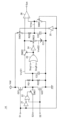
- FIG. 1 is a block diagram showing the configuration of a DC/DC converter 1 according to an embodiment.
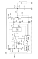
- 2 is a circuit diagram showing a configuration of an on-timer circuit 14 in FIG. 1.
- FIG. 3 is a timing chart showing changes in each signal in the on-timer circuit 14 of FIG. 2.
- FIG. It is a block diagram showing the composition of DC/DC converter 1A concerning the 1st modification of an embodiment.
- It is a block diagram showing the composition of DC/DC converter 1C concerning the 3rd modification of an embodiment.
- It is a block diagram showing the composition of DC/DC converter 1D concerning the 4th modification of an embodiment.
- FIG. 16 is a circuit diagram showing the configuration of an on-timer circuit 14I in FIG. 15.
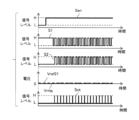
- FIG. 16 is a timing chart showing changes in each signal of the on-timer circuit 14I when the duty ratio of the switching elements Q1 and Q2 in FIG. 15 is 25%.
- 16 is a timing chart showing changes in each signal of the on-timer circuit 14I when the duty ratio of the switching elements Q1 and Q2 of FIG. 15 is 50%.
- 16 is a timing chart showing changes in each signal of the on-timer circuit 14I when the duty ratio of the switching elements Q1 and Q2 of FIG. 15 is 75%.
- 16 is a timing chart showing changes in each signal of the on-timer circuit 14I immediately after the DC/DC converter 1I of FIG. 15 is activated.
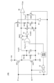
- FIG. 1 is a block diagram showing the configuration of a DC/DC converter 1 according to an embodiment.
- the DC/DC converter 1 includes switching elements Q1 and Q2, an inductor L1, a capacitor C1, and a control circuit 10.
- Switching elements Q1 and Q2 are connected in series with each other between input voltage source Vdd and ground. Switching elements Q1 and Q2 are provided on the high side and low side, respectively.
- the switching element Q1 is, for example, a P-channel field effect transistor, and the switching element Q2 is, for example, an N-channel field effect transistor.
- Inductor L1 is connected between the node between switching elements Q1 and Q2 and the output terminal Nout of DC/DC converter 1.
- Capacitor C1 is connected between the output terminal Nout of DC/DC converter 1 and ground.
- the control circuit 10 generates drive signals S1 and S2 that control on/off of each switching element Q1 and Q2, and applies the drive signals S1 and S2 to control electrodes (gates) of each switching element Q1 and Q2. Thereby, the control circuit 10 controls the switching elements Q1 and Q2 to store and release energy to the inductor L1.
- the DC/DC converter 1 receives an input voltage Vin from an input voltage source Vdd, generates an output voltage Vout at its output terminal Nout, and supplies the output voltage Vout to the load device 2.
- the DC/DC converter 1 is an example of a step-down converter that generates an output voltage Vout lower than the input voltage Vin.
- the control circuit 10 includes resistors R11 and R12, a reference voltage source E11, a comparator 11, a latch circuit 12, a driver circuit 13, an on-timer circuit 14, and a soft start circuit 31.
- Control circuit 10 may be configured as an integrated circuit having terminals N0 to N4.
- the resistors R11 and R12 are voltage dividing resistors connected in series with each other. Resistors R11 and R12 divide the output voltage Vout applied via the terminal N0 at a predetermined voltage division ratio, and input the divided voltage Vdiv to the inverting input terminal of the comparator 11.
- the reference voltage source E11 generates a variable reference voltage Vref11 in response to a signal Sss (described later) output from the soft start circuit 31, and inputs it to the non-inverting input terminal of the comparator 11.
- the reference voltage Vref11 When the signal Sss is at a low level, the reference voltage Vref11 is set to a first value corresponding to the desired voltage to be supplied from the DC/DC converter 1 to the load device 2.
- the reference voltage Vref11 is set to slowly increase from a second value (for example, 0V) lower than the first value to the first value.
- a second value for example, 0V
- the comparator 11 compares the voltage Vdiv with the reference voltage Vref11 and inputs a signal Scmp indicating the comparison result to the S terminal of the latch circuit 12.
- a signal Sot (described later) output from the on-timer circuit 14 is input to the R terminal of the latch circuit 12.
- the latch circuit 12 generates a signal having a high level or low level value expressed by a predetermined truth table according to the signals Scmp and Sot input from the comparator 11 and the on-timer circuit 14, respectively, and supplies the signal to the driver circuit 13. send.
- the driver circuit 13 generates drive signals S1 and S2, and applies the drive signals S1 and S2 to the control electrodes of the switching elements Q1 and Q2 via terminals N1 and N2, respectively.
- the driver circuit 13 operates the switching elements Q1 and Q2 under constant on-time control. In each switching cycle of switching elements Q1 and Q2, when voltage Vdiv falls below reference voltage Vref11, driver circuit 13 turns on switching element Q1 and turns off switching element Q2 for a predetermined time length, As a result, energy is accumulated in the inductor L1 (on section). After the on period has elapsed, the driver circuit 13 turns off the switching element Q1 and turns on the switching element Q2, thereby releasing the energy stored in the inductor L1 (rectification period). Furthermore, since the latch circuit 12 operates according to the signal Sot (described later) output from the on-timer circuit 14, the driver circuit 13 operates the switching elements Q1 and Q2 so as to end the on period according to the signal Sot.
- the drive signals S1 and S2 are input to the on-timer circuit 14, and a signal S3 indicating the voltage at the node between the switching elements Q1 and Q2 is input via the terminal N3. Further, the on-timer circuit 14 receives a signal generated by some kind of monitoring circuit, which indicates whether the DC/DC converter 1 is in a steady state or in an abnormal state.
- the steady state of the DC/DC converter 1 means that parameters such as the input voltage Vin, the output voltage Vout, and the output current Iout are within desired ranges during operation of the DC/DC converter 1.
- the abnormal state of the DC/DC converter 1 means that at least one of the parameters, such as the input voltage Vin, the output voltage Vout, and the output current Iout, is outside a desired range during operation of the DC/DC converter 1.
- the soft start circuit 31 is a monitoring circuit, and the signal Sss generated by the soft start circuit 31 is used as a signal indicating whether the DC/DC converter 1 is in a steady state or in an abnormal state.
- the signal is input to the on-timer circuit 14.
- the soft start circuit 31 controls the reference voltage source E11 so that the DC/DC converter 1 performs a soft start at startup in response to a signal Sen input from the outside of the DC/DC converter 1 via the terminal N4.
- the soft start of the DC/DC converter 1 is performed by slowly increasing the output voltage Vout from 0V to the desired voltage of the load device 2 after starting the DC/DC converter 1 in order to prevent input current rush and output voltage overshoot. It means to increase.
- the time period during which the output voltage Vout slowly increases from 0V and reaches the desired voltage of the load device 2 after the DC/DC converter 1 is started is referred to as a "soft start period.”
- the soft start circuit 31 generates a signal Sss indicating whether or not the DC/DC converter 1 is in a soft start period, and sends it to the reference voltage source E11. For example, when the signal Sss is at a high level, the DC/DC converter 1 is in a soft start period, and when the signal Sss is at a low level, the DC/DC converter 1 is not in a soft start period.
- the soft start circuit 31 When the DC/DC converter 1 is in the soft start period, the output voltage Vout is less than the desired voltage of the load device 2, so the DC/DC converter 1 is in an abnormal state. On the other hand, after the soft start period has elapsed, it is considered that the output voltage Vout reaches the desired voltage of the load device 2, and the DC/DC converter 1 is likely to be in a steady state. In other words, the signal Sss indicates whether the DC/DC converter 1 is in a steady state or in an abnormal state. Further, as described above, the soft start circuit 31 also sends the signal Sss to the on-timer circuit 14.
- the on-timer circuit 14 generates a signal Sot that ends the on-period of each switching period of the switching elements Q1 and Q2 based on the signals S1, S2, S3, and Sss, and outputs the signal Sot to the driver circuit 13 via the latch circuit 12. send to The on-timer circuit 14 generates the signal Sot using different reference voltages depending on the signal Sss, as explained below.
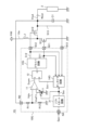
- FIG. 2 is a circuit diagram showing the configuration of the on-timer circuit 14 of FIG. 1.
- the on-timer circuit 14 includes inverters 21, 24, 25, NOR circuits 22, 23, a comparator 26, capacitors C21, C22, a reference voltage source E21, switching elements Q21, Q22, resistors R21 to R23, and It includes switches SW21 to SW25.
- Drive signals S1 and S2 are input to the on-timer circuit 14, and a signal S3 indicating the voltage at the node between the switching elements Q1 and Q2 is also input. Further, the signal Sss output from the soft start circuit 31 is input to the on-timer circuit 14, and the signal Sss is treated as one of the signals Strg1 to StrgK.
- the switching elements Q21 and Q22 are connected in series with each other between the input voltage source Vdd and ground. Switching elements Q21 and Q22 are provided on the high side and low side, respectively.
- the switching element Q21 is, for example, a P-channel field effect transistor, and the switching element Q22 is, for example, an N-channel field effect transistor.
- Drive signals S1 and S2 are applied to control electrodes (gates) of each switching element Q21 and Q22, respectively.
- Switching elements Q21 and Q22 are configured similarly to switching elements Q1 and Q2, and operate similarly to switching elements Q1 and Q2. Therefore, switching elements Q21 and Q22 generate a voltage that changes at the node between switching elements Q21 and Q22 in the same way as the voltage at the node between switching elements Q1 and Q2.
- the signal S3 is applied to the node between the switching elements Q21 and Q22 via the switch SW21.
- the inverter 21 and the NOR circuit 22 turn off the switch SW21 when one of the switching elements Q21 and Q22 is turned on, and turn on the switch SW21 when both of the switching elements Q21 and Q22 are turned off.
- the resistors R21 and R22 are voltage dividing resistors connected in series with each other. Resistors R21 and R22 divide the node between switching elements Q21 and Q22 at a predetermined voltage division ratio, and capacitor C21 is charged with the divided voltage. When switching elements Q1 and Q2 operate at a predetermined switching frequency, switching elements Q21 and Q22 also operate at the same switching frequency, and capacitor C21 is charged by the voltage generated by switching elements Q21 and Q22. On the other hand, when both switching elements Q1 and Q2 are turned off (for example, when pulse frequency modulation is used), both switching elements Q21 and Q22 are also turned off, and capacitor C21 is charged by the voltage of signal S3.
- the voltage of capacitor C21 changes depending on the duty ratio of switching elements Q1 and Q2.
- the voltage of capacitor C21 is used as a variable reference voltage Vref21.
- the reference voltage Vref21 is input to the inverting input terminal of the comparator 26.
- the switch SW24, the resistor R23, and the capacitor C22 are connected in series with each other between the input voltage source Vdd and ground.
- the switch SW24 is turned on/off according to the inverted signal of the signal S1 inverted by the inverter 25. Both ends of the capacitor C22 are short-circuited by a switch SW25 that is turned on/off according to the signal S1.
- the voltage Vrmp of the capacitor C22 gradually increases when the switching element Q1 is turned on, and becomes zero when the switching element Q1 is turned off. Voltage Vrmp is input to the non-inverting input terminal of comparator 26.
- the NOR circuit 23, the inverter 24, the reference voltage source E21, and the switches SW22 and SW23 use a fixed reference voltage Vref22 as a comparator instead of the variable reference voltage Vref21.
- Reference voltage source E21 generates a fixed reference voltage Vref22.
- the NOR circuit 23 receives as input signals Strg1 to StrgK indicating whether the DC/DC converter 1 is in a steady state or in an abnormal state from one or more monitoring circuits.
- the soft start circuit 31 is the monitoring circuit, but alternatively or additionally, the NOR circuit 23 can receive signals Strg1 to StrgK as inputs from other monitoring circuits as described with reference to FIGS. 4 to 9.
- the NOR circuit 23 and the inverter 24 switch SW22 and SW23 so as to send the reference voltage Vref21 to the comparator 26 when all of the signals Strg1 to StrgK are at a low level (that is, when no abnormal condition has occurred). control.
- the NOR circuit 23 and the inverter 24 are switched to send the reference voltage Vref22 to the comparator 26 when at least one of the signals Strg1 to StrgK is at a high level (that is, when some abnormal state has occurred). Controls SW22 and SW23.
- the comparator 26 generates a signal Sot by comparing the voltage Vrmp with the reference voltage Vref21 or Vref22 and sends it to the latch circuit 12.
- the on-timer circuit 14 generates the second control signal Sot that ends the on-period of each switching period of the switching elements Q1 and Q2 based on the first control signal Sss, and sends the second control signal Sot to the driver circuit 13. send.
- the on-timer circuit 14 When the DC/DC converter 1 is in a steady state, the on-timer circuit 14 generates a control signal Sot using a first reference voltage Vref21 that changes depending on the duty ratio of the switching elements Q1 and Q2.
- the on-timer circuit 14 generates the control signal Sot using the fixed second reference voltage Vref22 when the DC/DC converter 1 is in an abnormal state.
- control circuit 10 of the DC/DC converter 1 by including the on-timer circuit 14 of FIG. 2, even when the operation of the switching elements Q1 and Q2 deviates from its steady state, The DC/DC converter 1 can be controlled to perform constant on-time control with less variation in switching frequency than before.
- control circuit 10 of the DC/DC converter 1 according to the embodiment will be described in more detail with reference to a DC/DC converter according to a comparative example.
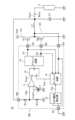
- FIG. 15 is a block diagram showing the configuration of a DC/DC converter 1I according to a comparative example.
- the DC/DC converter 1I includes an on-timer circuit 14I in place of the on-timer circuit 14 in FIG.
- the signal Sss generated by the soft start circuit 31 is not input to the on-timer circuit 14I.
- FIG. 16 is a circuit diagram showing the configuration of the on-timer circuit 14I of FIG. 15.
- the on-timer circuit 14I has a configuration in which the NOR circuit 23, the inverter 24, the reference voltage source E21, and the switches SW22 and SW23 are removed from the on-timer circuit 14 in FIG.
- the on-timer circuit 14I generates the signal Sot using only the variable reference voltage Vref21.
- FIG. 17 is a timing chart showing changes in each signal of the on-timer circuit 14I when the duty ratio of switching elements Q1 and Q2 in FIG. 15 is 25%.
- FIG. 18 is a timing chart showing changes in each signal of the on-timer circuit 14I when the duty ratio of the switching elements Q1 and Q2 of FIG. 15 is 50%.
- FIG. 19 is a timing chart showing changes in each signal of the on-timer circuit 14I when the duty ratio of the switching elements Q1 and Q2 of FIG. 15 is 75%.
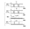
- Signals S1, S2, and Sot transition between high level (H) and low level (L). Voltage Vrmp gradually increases when switching element Q1 is turned on, and becomes zero when switching element Q1 is turned off.
- Reference voltage Vref21 changes according to the duty ratio of switching elements Q1 and Q2.
- voltage Vrmp reaches reference voltage Vref21
- signal Sot transitions from low level to high level.
- FIGS. 17 to 19 when the DC/DC converter 1 is in a steady state, the on period is ended by comparing the voltage Vrmp with the variable reference voltage Vref21, and the switching elements Q1 and Q2 are switched at a constant switching frequency. It can be operated with.
- FIG. 20 is a timing chart showing changes in each signal of the on-timer circuit 14I immediately after the DC/DC converter 1I of FIG. 15 is started.
- FIG. 20 shows a case where, immediately after the DC/DC converter 1I is started, the output voltage Vout is close to 0V, the reference voltage Vref21 becomes significantly low, and as a result, the period at which the on period ends becomes very short.
- the reference voltage Vref21 changes depending on the duty ratio of the switching elements Q1 and Q2. Therefore, if the operation of the switching elements Q1, Q2 deviates from its steady state, for example, immediately after the startup of the DC/DC converter 1I or when the ground fault protection circuit is activated, the switching elements Q1, Q2 can be adjusted to the desired state. Unable to operate at switching frequency.
- FIG. 3 is a timing chart showing changes in each signal in the on-timer circuit 14 of FIG.
- the variable reference voltage Vref21 and the fixed reference voltage Vref22 are selectively used.
- the DC/DC converter 1 is in the soft start period, that is, when the signal Sss is at a high level, the fixed reference voltage Vref22 is used, and when the signal Sss is at a low level, the variable reference voltage Vref21 is used.
- Ru When voltage Vrmp reaches reference voltage Vref21 or Vref22, signal Sot transitions from low level to high level.
- the switching elements Q1 and Q2 operate at a desired switching frequency.
- the control circuit 10 of the DC/DC converter 1 according to the embodiment even when the operation of the switching elements Q1 and Q2 deviates from its steady state, fluctuations in the switching frequency can be reduced compared to the conventional one.
- DC/DC converter 1 can be controlled to perform constant on-time control.
- the control circuit 10 of the DC/DC converter 1 according to the embodiment even if the operation of the switching elements Q1 and Q2 deviates from its steady state, it is preferable to maintain constant on-time at a constant switching frequency.
- the DC/DC converter 1 can be controlled to implement the control.
- the soft-start circuit 31 is the monitoring circuit, but alternatively or additionally, the NOR circuit 23 of FIG. 2 may be any other monitoring circuit as described with reference to FIGS.
- the signals Strg1 to StrgK may be obtained as inputs from the following.
- FIG. 4 is a block diagram showing the configuration of a DC/DC converter 1A according to a first modification of the embodiment.
- the DC/DC converter 1A includes a control circuit 10A instead of the control circuit 10 in FIG.
- the control circuit 10A includes a voltage drop detector 32 and a delay circuit 33 in addition to the components shown in FIG. In FIGS. 4 to 9, illustration of the soft start circuit 31 is omitted.
- Voltage drop detector 32 is an example of a monitoring circuit. The voltage drop detector 32 acquires the input voltage Vin of the DC/DC converter 1A via the terminal N5, and detects the magnitude of the input voltage Vin.
- the voltage drop detector 32 generates a signal Suvin indicating whether the input voltage Vin is in a steady state equal to or higher than a threshold value or in an abnormal state lower than the threshold value, and outputs a signal Suvin via a delay circuit 33. is sent to the on-timer circuit 14. For example, when the input voltage Vin is greater than or equal to the threshold value, the signal Suvin is set to a low level, and when the input voltage Vin is less than the threshold value, the signal Suvin is set to a high level.
- the signal Suvin is treated as one of the signals Strg1 to StrgK input to the NOR circuit 23.
- FIG. 5 is a block diagram showing the configuration of a DC/DC converter 1B according to a second modification of the embodiment.
- the DC/DC converter 1B includes a control circuit 10B in place of the control circuit 10 in FIG.
- the control circuit 10B includes a voltage drop detector 34 in addition to the components shown in FIG.
- Voltage drop detector 34 is an example of a monitoring circuit.
- the voltage drop detector 34 generates a signal Suvout indicating whether the output voltage Vout is in a steady state equal to or higher than the threshold value or in an abnormal state lower than the threshold value, and sends it to the on-timer circuit 14.
- the signal Suvout when the output voltage Vout is greater than or equal to the threshold value, the signal Suvout is set to a low level, and when the output voltage Vout is less than the threshold value, the signal Suvout is set to a high level.
- the signal Suvout is treated as one of the signals Strg1 to StrgK input to the NOR circuit 23.
- FIG. 6 is a block diagram showing the configuration of a DC/DC converter 1C according to a third modification of the embodiment.
- the DC/DC converter 1C includes a control circuit 10C in place of the control circuit 10 in FIG.
- the control circuit 10C includes a transient response detector 35 in addition to the components shown in FIG.
- Transient response detector 35 is an example of a monitoring circuit.
- Transient response detector 35 detects whether or not DC/DC converter 1 is in a transient response state due to load device 2 based on output voltage Vout.
- the transient response state means that the output voltage Vout fluctuates significantly during a predetermined time period due to a transient response of the load device 2 connected to the output terminal Nout of the DC/DC converter 1C.
- the transient response detector 35 generates a signal Sus indicating whether the DC/DC converter 1 is in a transient response state, that is, in an abnormal state, or in a steady state, and sends it to the on-timer circuit 14. For example, when the DC/DC converter 1 is in a transient response state, the signal Sus is set to a high level; otherwise, the signal Sus is set to a low level. The signal Sus is treated as one of the signals Strg1 to StrgK input to the NOR circuit 23.
- FIG. 7 is a block diagram showing the configuration of a DC/DC converter 1D according to a fourth modification of the embodiment.
- the DC/DC converter 1D includes a control circuit 10D instead of the control circuit 10 in FIG.
- the control circuit 10D includes a peak current detector 36 in addition to the components shown in FIG. Peak current detector 36 is an example of a monitoring circuit. Peak current detector 36 is connected to input voltage source Vdd via terminal N6 and to a node between switching elements Q1 and Q2 via terminal N3.
- the peak current detector 36 obtains the output current Iout (or the current flowing through the inductor L1) of the DC/DC converter 1D by monitoring the voltage across the switching element Q1 when the switching element Q1 is turned on, and outputs the output current Iout (or the current flowing through the inductor L1). The magnitude of the peak of current Iout is detected.
- the peak current detector 36 generates a signal Spc and sends it to the on-timer circuit 14, indicating whether the output current Iout is in a steady state where the peak is equal to or greater than the threshold value or in an abnormal state where the peak value is less than the threshold value.
- the signal Spc when the peak of the output current Iout is greater than or equal to the threshold value, the signal Spc is set to a low level, and when the peak of the output current Iout is less than the threshold value, the signal Spc is set to a high level.
- the signal Spc is treated as one of the signals Strg1 to StrgK input to the NOR circuit 23.
- FIG. 8 is a block diagram showing the configuration of a DC/DC converter 1E according to a fifth modification of the embodiment.
- the DC/DC converter 1E includes a control circuit 10E instead of the control circuit 10 in FIG.
- the control circuit 10E includes a zero current detector 37 in addition to the components shown in FIG.
- Zero current detector 37 is an example of a monitoring circuit.
- Zero current detector 37 is connected to a node between switching elements Q1 and Q2 via terminal N3, and grounded via terminal N7.
- the zero current detector 37 obtains the output current Iout of the DC/DC converter 1E by monitoring the voltage across the switching element Q2 when the switching element Q2 is turned on, and detects the direction in which the output current Iout flows. .
- the zero current detector 37 generates a signal Szc indicating whether the output current Iout is in a steady state flowing from the switching element Q2 toward the output terminal Nout or in an abnormal state flowing in the opposite direction, and outputs the signal Szc to the on-timer circuit 14. send. For example, when the output current Iout is flowing from the switching element Q2 toward the output terminal Nout, the signal Szc is set to a low level, and when the output current Iout is flowing in the opposite direction, the signal Szc is set to a high level. Ru. The signal Szc is treated as one of the signals Strg1 to StrgK input to the NOR circuit 23.
- FIG. 9 is a block diagram showing the configuration of a DC/DC converter 1F according to a sixth modification of the embodiment.
- the DC/DC converter 1F includes a control circuit 10F in place of the control circuit 10 in FIG.
- the control circuit 10F includes a reverse current detector 38 in addition to the components shown in FIG.
- Reverse current detector 38 is an example of a monitoring circuit.
- Reverse current detector 38 is connected to a node between switching elements Q1 and Q2 via terminal N3, and grounded via terminal N7.
- the reverse current detector 38 obtains the output current Iout of the DC/DC converter 1F by monitoring the voltage across the switching element Q2 when the switching element Q2 is turned on, and determines the flow direction and magnitude of the output current Iout. Detect.
- the reverse current detector 38 generates a signal Src indicating whether the output current Iout is in a steady state flowing from the switching element Q2 toward the output terminal Nout or in an abnormal state where it flows in the opposite direction and is larger than a threshold value. and sends it to the on-timer circuit 14. For example, when the output current Iout is flowing from the switching element Q2 toward the output terminal Nout, the signal Src is set to a low level, and when the output current Iout is flowing in the opposite direction and is larger than the threshold value, the signal Src is set to a high level. set to the level. The signal Src is treated as one of the signals Strg1 to StrgK input to the NOR circuit 23.
- control circuits 10A to 10F of the DC/DC converters 1A to 1F similarly to the control circuit 10 of FIG. 1, the variable reference voltage Vref21 and the fixed reference voltage Vref22 are selectively used, A control signal Sot can be generated to end the on period. As a result, even if the operation of switching elements Q1 and Q2 deviates from their steady state, the DC/DC converter 1A can reduce fluctuations in switching frequency more than before and perform constant on-time control. ⁇ 1F can be controlled.
- the configurations described with reference to FIGS. 1 and 4 to 9 may be combined.
- the NOR circuit 23 in FIG. 2 may receive signals Strg1 to StrgK from a plurality of monitoring circuits as input. This makes it possible to detect a plurality of events that each indicate whether the DC/DC converter is in a steady state or in an abnormal state.
- FIG. 10 is a block diagram showing a partial configuration of an on-timer circuit 14A according to a seventh modification of the embodiment.
- the on-timer circuit 14A may include reference voltage sources E21-1 to E21-K and switches SW23-1 to SW23-K in FIG. 10 instead of the inverter 24, reference voltage source E21, and switch SW23 in FIG. good.
- the reference voltage sources E21-1 to E21-K generate a plurality of mutually different reference voltages Vref22-1 to Vref22-K.
- the on-timer circuit 14A can generate a control signal Sot using a plurality of reference voltages Vref22-1 to Vref22-K that correspond to a plurality of events and are different from each other. Thereby, when detecting a plurality of events each indicating whether the DC/DC converter is in a steady state or in an abnormal state, an appropriate reference voltage can be used depending on the event.
- FIG. 11 is a block diagram showing the configuration of an on-timer circuit 14B according to an eighth modification of the embodiment.
- the on-timer circuit 14B includes a delay circuit 27 in place of the switch S21 in FIG.
- the output signal of the NOR circuit 22 is input to the NOR circuit 22 via the delay circuit 27.
- the on-timer circuit 14B uses the fixed reference voltage Vref22 to generate a control signal for a certain period of time after starting the switching operation. Sot can be generated.
- FIG. 12 is a block diagram showing the configuration of an on-timer circuit 14C according to a ninth modification of the embodiment.
- the on-timer circuit 14C has a configuration in which the inverter 21, NOR circuit 22, switching elements Q21, Q22, and switch SW21 of FIG. 2 are removed. Thereby, the on-timer circuit 14C has a simpler circuit configuration than the on-timer circuit 14 of FIG. 2, and can reduce size and cost.
- [Modified example of DC/DC converter] 1 to 12 show examples of DC/DC converters that are step-down converters.
- the control of the DC/DC converter according to the embodiment is also applicable to a boost converter or a buck-boost converter.
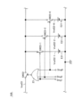
- FIG. 13 is a block diagram showing the configuration of a DC/DC converter 1G according to a tenth modification of the embodiment.
- the DC/DC converter 1G includes switching elements Q11, Q12, an inductor L1, a capacitor C1, and a control circuit 10G.
- Inductor L1 and switching element Q11 are connected in series with each other between input voltage source Vdd and ground.
- Switching element Q12 is connected between the node between inductor L1 and switching element Q11 and the output terminal Nout of DC/DC converter 1G.
- Switching elements Q11 and Q12 are provided on the low side and high side, respectively.
- the switching element Q11 is, for example, an N-channel field effect transistor, and the switching element Q12 is, for example, a P-channel field effect transistor.
- Capacitor C1 is connected between the output terminal Nout of DC/DC converter 1G and ground.
- the control circuit 10G generates drive signals S11 and S12 that control on/off of each switching element Q11 and Q12, and applies the drive signals S11 and S12 to the control electrodes (gates) of each switching element Q11 and Q12. Thereby, the control circuit 10G controls the switching elements Q11 and Q12 to store and release energy to the inductor L1.
- the DC/DC converter 1G is an example of a step-up converter that generates an output voltage Vout higher than the input voltage Vin.
- the control circuit 10G includes a driver circuit 13G and an on-timer circuit 14G in place of the driver circuit 13 and on-timer circuit 14 in FIG.
- the driver circuit 13G generates drive signals S11 and S12, and applies the drive signals S11 and S12 to the control electrodes of the switching elements Q11 and Q12 via terminals N11 and N12, respectively.
- the driver circuit 13G operates the switching elements Q11 and Q12 under constant on-time control. In each switching cycle of switching elements Q11 and Q12, when voltage Vdiv falls below reference voltage Vref11, driver circuit 13G turns on switching element Q11 and turns off switching element Q12 for a predetermined time length, As a result, energy is accumulated in the inductor L1 (on section).
- the driver circuit 13G After the on period has elapsed, the driver circuit 13G turns off the switching element Q11 and turns on the switching element Q12, thereby releasing the energy accumulated in the inductor L1 (rectification period). Further, since the latch circuit 12 operates according to the signal Sot, the driver circuit 13G operates the switching elements Q11 and Q12 so as to end the on period according to the signal Sot.
- Drive signals S11 and S12 are input to the on-timer circuit 14G, and a signal S13 indicating the output voltage Vout is input via the terminal N13. Further, the signal Sss generated by the soft start circuit 31 is input to the on-timer circuit 14G.
- the on-timer circuit 14G generates a signal Sot based on the signals S11, S12, S13, and Sss, and sends the signal Sot to the driver circuit 13G via the latch circuit 12.
- the on-timer circuit 14G like the on-timer circuit 14 in FIG. 1, generates the signal Sot by selectively using different reference voltages, that is, a variable reference voltage and a fixed reference voltage, depending on the signal Sss.
- signals S11, S12, and S13 generally correspond to signals S1, S2, and S3 in FIG. 2, respectively.
- the on-timer circuit 14G may include two switching elements that respectively operate according to the signals S11 and S12, similar to the on-timer circuit 14 in FIG. 2, and the on-timer circuit 14G in FIG. Similarly to 14C, signal S3 may be used.
- control circuit 10G of FIG. 13 similarly to the control circuit 10 of FIG. 1, it is possible to selectively use the variable reference voltage and the fixed reference voltage to generate the control signal Sot that ends the on period. can. As a result, even when the operation of switching elements Q11 and Q12 deviates from their steady state, the DC/DC converter 1G reduces fluctuations in switching frequency more than before and performs constant on-time control. can be controlled.
- the soft start circuit 31 is a monitoring circuit, but the DC/DC converter 1G, which is a step-up converter, may alternatively or additionally use other monitoring circuits as described with reference to FIGS. 4 to 9. You may prepare.
- FIG. 14 is a block diagram showing the configuration of a DC/DC converter 1H according to an eleventh modification of the embodiment.
- the DC/DC converter 1H includes switching elements Q1, Q2, Q11, Q12, an inductor L1, a capacitor C1, and a control circuit 10H.
- Switching elements Q1, Q2 and inductor L1 in FIG. 14 operate as part of a step-down converter, similar to the corresponding components in FIG.
- Switching elements Q11, Q12 and inductor L1 in FIG. 14 operate as part of a boost converter, similar to the corresponding components in FIG. 13.
- the control circuit 10H has the functions of both the control circuit 10 in FIG. 1 and the control circuit 10G in FIG. 13.
- the DC/DC converter 1H is an example of a buck-boost converter that generates both an output voltage Vout lower than the input voltage Vin and an output voltage Vout higher than the input voltage Vin. According to the control circuit 10H in FIG. 14, similarly to the control circuit 10 in FIG. 1 and the control circuit 10G in FIG. However, the DC/DC converter 1H can be controlled so as to perform constant on-time control with less variation in switching frequency than before.
- the switching elements Q1 and Q2 are provided outside the integrated circuit having the terminals N0 to N8, etc.
- the switching elements Q1 and Q2 may be integrated inside the control circuit 10. good.
- the resistor R21 may be configured to have an adjustable resistance value.
- the reference voltage source E21 may be configured to have an adjustable voltage value.
- the signal S3 indicating the voltage at the node between the switching elements Q1 and Q2 is used to generate the reference voltage Vref21 that changes according to the duty ratio of the switching elements Q1 and Q2, but the signal S3 The output voltage Vout may be used instead.
- a control circuit 10 for a DC/DC converter 1 includes an inductor L1 and first and second switching elements Q1 and Q2 that store and release energy with respect to the inductor L1. Controls the DC/DC converter 1.
- the control circuit 10 includes a driver circuit 13, a monitoring circuit, and an on-timer circuit 14.
- the driver circuit 13 operates the first and second switching elements Q1 and Q2 under constant on-time control.
- the monitoring circuit generates a first control signal indicating whether the DC/DC converter 1 is in a steady state or in an abnormal state.
- the on-timer circuit 14 determines a section in which energy is stored in the inductor L1, which is a section within each switching period of the first and second switching elements Q1 and Q2. A second control signal for termination is generated and sent to the driver circuit 13.
- the on-timer circuit 14 When the DC/DC converter 1 is in a steady state, the on-timer circuit 14 generates a second control signal using a first reference voltage that changes depending on the duty ratio of the first and second switching elements Q1 and Q2. Occur.
- the on-timer circuit 14 generates a second control signal using a fixed second reference voltage when the DC/DC converter 1 is in an abnormal state.
- control circuit 10 of the DC/DC converter 1 may be configured as follows.
- the monitoring circuit generates a first control signal indicating that the DC/DC converter 1 is in an abnormal state when the DC/DC converter 1 is in the soft start period.
- control circuit 10 of the DC/DC converter 1 may be configured as follows.
- the monitoring circuit generates a first control signal indicating that the DC/DC converter 1 is in an abnormal state when the input voltage of the DC/DC converter 1 is lower than a first threshold.
- control circuit 10 of the DC/DC converter 1 may be configured as follows.
- the monitoring circuit generates a first control signal indicating that the DC/DC converter 1 is in an abnormal state when the output voltage of the DC/DC converter 1 is lower than a second threshold.
- control circuit 10 of the DC/DC converter 1 may be configured as follows.
- the monitoring circuit generates a first control signal indicating that the DC/DC converter 1 is in an abnormal state when the DC/DC converter 1 is in a transient response state due to a load.
- control circuit 10 of the DC/DC converter 1 may be configured as follows.
- the monitoring circuit generates a first control signal indicating that the DC/DC converter 1 is in an abnormal state when the peak of the output current of the DC/DC converter 1 is smaller than a third threshold.
- control circuit 10 of the DC/DC converter 1 may be configured as follows.
- the monitoring circuit detects a reverse flow of the output current of the DC/DC converter 1, it generates a first control signal indicating that the DC/DC converter 1 is in an abnormal state.
- control circuit 10 of the DC/DC converter 1 may be configured as follows.
- the monitoring circuit generates a first control signal indicating that the DC/DC converter 1 is in an abnormal state when the output current of the DC/DC converter 1 flows backward and is greater than a fourth threshold.
- control circuit 10 of the DC/DC converter 1 may be configured as follows.
- the monitoring circuit detects a plurality of events each indicating that the DC/DC converter 1 is in an abnormal state.
- the on-timer circuit 14 generates control signals using a plurality of different second reference voltages, each corresponding to a plurality of events.
- control circuit 10 of the DC/DC converter 1 may be configured as follows.
- the on-timer circuit 14 uses a fixed second reference voltage for a certain period of time after starting the switching operation.
- a control signal is generated using
- a DC/DC converter 1 according to an eleventh aspect of the present disclosure includes first and second switching elements Q1 and Q2 provided on the high side and low side, respectively, and a DC/DC converter 1 according to one of the first to tenth aspects.
- a control circuit 10 is provided.
Landscapes
- Engineering & Computer Science (AREA)
- Power Engineering (AREA)
- Dc-Dc Converters (AREA)
Priority Applications (4)
| Application Number | Priority Date | Filing Date | Title |
|---|---|---|---|
| US18/865,030 US20250317059A1 (en) | 2022-06-06 | 2022-06-06 | Dc/dc converter capable of performing constant on-time control with reduced variations of switching frequency |
| PCT/JP2022/022828 WO2023238201A1 (ja) | 2022-06-06 | 2022-06-06 | Dc/dcコンバータ |
| JP2024526049A JPWO2023238201A1 (https=) | 2022-06-06 | 2022-06-06 | |
| CN202280096796.8A CN119318106A (zh) | 2022-06-06 | 2022-06-06 | Dc/dc转换器 |
Applications Claiming Priority (1)
| Application Number | Priority Date | Filing Date | Title |
|---|---|---|---|
| PCT/JP2022/022828 WO2023238201A1 (ja) | 2022-06-06 | 2022-06-06 | Dc/dcコンバータ |
Publications (1)
| Publication Number | Publication Date |
|---|---|
| WO2023238201A1 true WO2023238201A1 (ja) | 2023-12-14 |
Family
ID=89117991
Family Applications (1)
| Application Number | Title | Priority Date | Filing Date |
|---|---|---|---|
| PCT/JP2022/022828 Ceased WO2023238201A1 (ja) | 2022-06-06 | 2022-06-06 | Dc/dcコンバータ |
Country Status (4)
| Country | Link |
|---|---|
| US (1) | US20250317059A1 (https=) |
| JP (1) | JPWO2023238201A1 (https=) |
| CN (1) | CN119318106A (https=) |
| WO (1) | WO2023238201A1 (https=) |
Citations (5)
| Publication number | Priority date | Publication date | Assignee | Title |
|---|---|---|---|---|
| US7541795B1 (en) * | 2006-02-09 | 2009-06-02 | National Semiconductor Corporation | Apparatus and method for start-up and over-current protection for a regulator |
| US20150042299A1 (en) * | 2013-08-12 | 2015-02-12 | Chengdu Monolithic Power Systems Co., Ltd. | Soft start switching power supply system |
| US20180131379A1 (en) * | 2016-11-08 | 2018-05-10 | Chengdu Monolithic Power Systems Co., Ltd. | Cot control circuit and associated dc-dc converter |
| JP2020120546A (ja) * | 2019-01-28 | 2020-08-06 | ローム株式会社 | 電源装置 |
| US20210028701A1 (en) * | 2019-01-04 | 2021-01-28 | Silanna Asia Pte Ltd | Constant On-Time Converter with Frequency Control |
-
2022
- 2022-06-06 WO PCT/JP2022/022828 patent/WO2023238201A1/ja not_active Ceased
- 2022-06-06 US US18/865,030 patent/US20250317059A1/en active Pending
- 2022-06-06 CN CN202280096796.8A patent/CN119318106A/zh active Pending
- 2022-06-06 JP JP2024526049A patent/JPWO2023238201A1/ja active Pending
Patent Citations (5)
| Publication number | Priority date | Publication date | Assignee | Title |
|---|---|---|---|---|
| US7541795B1 (en) * | 2006-02-09 | 2009-06-02 | National Semiconductor Corporation | Apparatus and method for start-up and over-current protection for a regulator |
| US20150042299A1 (en) * | 2013-08-12 | 2015-02-12 | Chengdu Monolithic Power Systems Co., Ltd. | Soft start switching power supply system |
| US20180131379A1 (en) * | 2016-11-08 | 2018-05-10 | Chengdu Monolithic Power Systems Co., Ltd. | Cot control circuit and associated dc-dc converter |
| US20210028701A1 (en) * | 2019-01-04 | 2021-01-28 | Silanna Asia Pte Ltd | Constant On-Time Converter with Frequency Control |
| JP2020120546A (ja) * | 2019-01-28 | 2020-08-06 | ローム株式会社 | 電源装置 |
Also Published As
| Publication number | Publication date |
|---|---|
| CN119318106A (zh) | 2025-01-14 |
| JPWO2023238201A1 (https=) | 2023-12-14 |
| US20250317059A1 (en) | 2025-10-09 |
Similar Documents
| Publication | Publication Date | Title |
|---|---|---|
| CN110504834B (zh) | 开关频率控制设备及其控制方法 | |
| US9172300B2 (en) | Charge-pump voltage divider and associated control method | |
| EP2994986B1 (en) | Buck-boost switching converter with buck-boost transition switching control and corresponding method | |
| JP5768475B2 (ja) | スイッチング電源装置 | |
| US7843186B2 (en) | Switching regulator having high speed response | |
| JP6783776B2 (ja) | スイッチングレギュレータ及びその制御方法 | |
| US9013165B2 (en) | Switching regulator including a configurable multi-mode PWM controller implementing multiple control schemes | |
| JP5458686B2 (ja) | 降圧型コンバータ | |
| KR20170120605A (ko) | 유한 상태 기계 제어를 사용하는 다중-레벨 스위칭 조절기 회로들 및 방법들 | |
| US8030909B2 (en) | Method and apparatus for switching a synchronous DC/DC converter between a PWM mode of operation and a light-load mode of operation | |
| JP4998094B2 (ja) | Dc−dcコンバータ | |
| CN212572391U (zh) | 电子电路 | |
| US9455632B1 (en) | Voltage converter | |
| JP2020089043A (ja) | スイッチング電源用回路 | |
| US8502508B2 (en) | Switching regulator circuit configured to perform step up and step down operations and operation method therefor | |
| TWI710202B (zh) | 開關調節器 | |
| CN114726209A (zh) | 用于升压转换器的具有可调环路增益的反馈电路 | |
| WO2023238201A1 (ja) | Dc/dcコンバータ | |
| JP6710104B2 (ja) | 電源装置および電源制御方法 | |
| JP5168082B2 (ja) | 昇降圧dc−dcコンバータ制御回路、および昇降圧dc−dcコンバータ制御方法 | |
| JP3623934B2 (ja) | 昇降圧コンバータ | |
| WO2023238241A1 (ja) | スイッチングレギュレータ | |
| US20160352123A1 (en) | Power supply apparatus | |
| JP2022165745A (ja) | Dc/dcコンバータおよびその制御回路、ならびに電子機器 | |
| JP7855070B2 (ja) | スイッチングレギュレータ |
Legal Events
| Date | Code | Title | Description |
|---|---|---|---|
| 121 | Ep: the epo has been informed by wipo that ep was designated in this application |
Ref document number: 22945711 Country of ref document: EP Kind code of ref document: A1 |
|
| WWE | Wipo information: entry into national phase |
Ref document number: 2024526049 Country of ref document: JP |
|
| WWE | Wipo information: entry into national phase |
Ref document number: 202280096796.8 Country of ref document: CN |
|
| NENP | Non-entry into the national phase |
Ref country code: DE |
|
| WWP | Wipo information: published in national office |
Ref document number: 202280096796.8 Country of ref document: CN |
|
| 122 | Ep: pct application non-entry in european phase |
Ref document number: 22945711 Country of ref document: EP Kind code of ref document: A1 |
|
| WWP | Wipo information: published in national office |
Ref document number: 18865030 Country of ref document: US |