WO2023234383A1 - 弾性波装置および通信装置 - Google Patents
弾性波装置および通信装置 Download PDFInfo
- Publication number
- WO2023234383A1 WO2023234383A1 PCT/JP2023/020400 JP2023020400W WO2023234383A1 WO 2023234383 A1 WO2023234383 A1 WO 2023234383A1 JP 2023020400 W JP2023020400 W JP 2023020400W WO 2023234383 A1 WO2023234383 A1 WO 2023234383A1
- Authority
- WO
- WIPO (PCT)
- Prior art keywords
- less
- thickness
- electrode
- wave device
- elastic wave
- Prior art date
Links
- 239000000758 substrate Substances 0.000 claims abstract description 23
- WSMQKESQZFQMFW-UHFFFAOYSA-N 5-methyl-pyrazole-3-carboxylic acid Chemical compound CC1=CC(C(O)=O)=NN1 WSMQKESQZFQMFW-UHFFFAOYSA-N 0.000 claims description 140
- 239000000463 material Substances 0.000 claims description 71
- 239000000470 constituent Substances 0.000 claims description 62
- 229910052751 metal Inorganic materials 0.000 claims description 19
- 239000002184 metal Substances 0.000 claims description 19
- GQYHUHYESMUTHG-UHFFFAOYSA-N lithium niobate Chemical compound [Li+].[O-][Nb](=O)=O GQYHUHYESMUTHG-UHFFFAOYSA-N 0.000 claims description 11
- 235000019687 Lamb Nutrition 0.000 abstract description 5
- 238000004088 simulation Methods 0.000 description 237
- 239000010410 layer Substances 0.000 description 124
- 239000013256 coordination polymer Substances 0.000 description 102
- BASFCYQUMIYNBI-UHFFFAOYSA-N platinum Substances [Pt] BASFCYQUMIYNBI-UHFFFAOYSA-N 0.000 description 58
- 239000010949 copper Substances 0.000 description 57
- 239000007772 electrode material Substances 0.000 description 30
- 238000010897 surface acoustic wave method Methods 0.000 description 18
- 230000005540 biological transmission Effects 0.000 description 10
- 239000000654 additive Substances 0.000 description 8
- 230000000996 additive effect Effects 0.000 description 8
- 239000012535 impurity Substances 0.000 description 8
- 239000000956 alloy Substances 0.000 description 6
- 229910045601 alloy Inorganic materials 0.000 description 6
- 229910052782 aluminium Inorganic materials 0.000 description 6
- 238000010586 diagram Methods 0.000 description 6
- 229920006395 saturated elastomer Polymers 0.000 description 6
- 229910052802 copper Inorganic materials 0.000 description 5
- 238000004519 manufacturing process Methods 0.000 description 5
- 229910004298 SiO 2 Inorganic materials 0.000 description 4
- 238000012886 linear function Methods 0.000 description 4
- 239000007769 metal material Substances 0.000 description 4
- 229910052697 platinum Inorganic materials 0.000 description 4
- VYPSYNLAJGMNEJ-UHFFFAOYSA-N Silicium dioxide Chemical compound O=[Si]=O VYPSYNLAJGMNEJ-UHFFFAOYSA-N 0.000 description 3
- ATJFFYVFTNAWJD-UHFFFAOYSA-N Tin Chemical group [Sn] ATJFFYVFTNAWJD-UHFFFAOYSA-N 0.000 description 3
- 230000004048 modification Effects 0.000 description 3
- 238000012986 modification Methods 0.000 description 3
- 229910013641 LiNbO 3 Inorganic materials 0.000 description 2
- XAGFODPZIPBFFR-UHFFFAOYSA-N aluminium Chemical compound [Al] XAGFODPZIPBFFR-UHFFFAOYSA-N 0.000 description 2
- 239000013078 crystal Substances 0.000 description 2
- 238000002149 energy-dispersive X-ray emission spectroscopy Methods 0.000 description 2
- 239000000395 magnesium oxide Substances 0.000 description 2
- CPLXHLVBOLITMK-UHFFFAOYSA-N magnesium oxide Inorganic materials [Mg]=O CPLXHLVBOLITMK-UHFFFAOYSA-N 0.000 description 2
- AXZKOIWUVFPNLO-UHFFFAOYSA-N magnesium;oxygen(2-) Chemical compound [O-2].[Mg+2] AXZKOIWUVFPNLO-UHFFFAOYSA-N 0.000 description 2
- 239000000203 mixture Substances 0.000 description 2
- 230000001902 propagating effect Effects 0.000 description 2
- 239000011241 protective layer Substances 0.000 description 2
- 230000005236 sound signal Effects 0.000 description 2
- 238000000177 wavelength dispersive X-ray spectroscopy Methods 0.000 description 2
- RYGMFSIKBFXOCR-UHFFFAOYSA-N Copper Chemical compound [Cu] RYGMFSIKBFXOCR-UHFFFAOYSA-N 0.000 description 1
- WHXSMMKQMYFTQS-UHFFFAOYSA-N Lithium Chemical group [Li] WHXSMMKQMYFTQS-UHFFFAOYSA-N 0.000 description 1
- GWEVSGVZZGPLCZ-UHFFFAOYSA-N Titan oxide Chemical compound O=[Ti]=O GWEVSGVZZGPLCZ-UHFFFAOYSA-N 0.000 description 1
- MCMNRKCIXSYSNV-UHFFFAOYSA-N ZrO2 Inorganic materials O=[Zr]=O MCMNRKCIXSYSNV-UHFFFAOYSA-N 0.000 description 1
- 239000002253 acid Substances 0.000 description 1
- 230000002411 adverse Effects 0.000 description 1
- 239000012141 concentrate Substances 0.000 description 1
- 230000007423 decrease Effects 0.000 description 1
- 230000005284 excitation Effects 0.000 description 1
- CJNBYAVZURUTKZ-UHFFFAOYSA-N hafnium(iv) oxide Chemical compound O=[Hf]=O CJNBYAVZURUTKZ-UHFFFAOYSA-N 0.000 description 1
- 230000012447 hatching Effects 0.000 description 1
- 239000011810 insulating material Substances 0.000 description 1
- 229910052744 lithium Inorganic materials 0.000 description 1
- 238000000034 method Methods 0.000 description 1
- BPUBBGLMJRNUCC-UHFFFAOYSA-N oxygen(2-);tantalum(5+) Chemical compound [O-2].[O-2].[O-2].[O-2].[O-2].[Ta+5].[Ta+5] BPUBBGLMJRNUCC-UHFFFAOYSA-N 0.000 description 1
- RVTZCBVAJQQJTK-UHFFFAOYSA-N oxygen(2-);zirconium(4+) Chemical compound [O-2].[O-2].[Zr+4] RVTZCBVAJQQJTK-UHFFFAOYSA-N 0.000 description 1
- 230000001681 protective effect Effects 0.000 description 1
- 235000012239 silicon dioxide Nutrition 0.000 description 1
- 239000000377 silicon dioxide Substances 0.000 description 1
- LIVNPJMFVYWSIS-UHFFFAOYSA-N silicon monoxide Chemical compound [Si-]#[O+] LIVNPJMFVYWSIS-UHFFFAOYSA-N 0.000 description 1
- 229910052814 silicon oxide Inorganic materials 0.000 description 1
- 229910052715 tantalum Inorganic materials 0.000 description 1
- GUVRBAGPIYLISA-UHFFFAOYSA-N tantalum atom Chemical compound [Ta] GUVRBAGPIYLISA-UHFFFAOYSA-N 0.000 description 1
- PBCFLUZVCVVTBY-UHFFFAOYSA-N tantalum pentoxide Inorganic materials O=[Ta](=O)O[Ta](=O)=O PBCFLUZVCVVTBY-UHFFFAOYSA-N 0.000 description 1
Images


Classifications
-
- H—ELECTRICITY
- H03—ELECTRONIC CIRCUITRY
- H03H—IMPEDANCE NETWORKS, e.g. RESONANT CIRCUITS; RESONATORS
- H03H9/00—Networks comprising electromechanical or electro-acoustic devices; Electromechanical resonators
- H03H9/02—Details
- H03H9/125—Driving means, e.g. electrodes, coils
- H03H9/145—Driving means, e.g. electrodes, coils for networks using surface acoustic waves
-
- H—ELECTRICITY
- H03—ELECTRONIC CIRCUITRY
- H03H—IMPEDANCE NETWORKS, e.g. RESONANT CIRCUITS; RESONATORS
- H03H9/00—Networks comprising electromechanical or electro-acoustic devices; Electromechanical resonators
- H03H9/25—Constructional features of resonators using surface acoustic waves
Definitions
- the present disclosure relates to an elastic wave device and a communication device.
- acoustic wave elements that have a structure in which an IDT (Interdigital Transducer) electrode is formed on a piezoelectric crystal.
- Acoustic wave elements can be used, for example, as filters (SAW filters) that excite surface acoustic waves (SAW) near a specific frequency and receive electrical signals near a specific frequency, and are used in communication equipment. It is used in bandpass filters and the like (see, for example, Patent Document 1).
- An acoustic wave device includes a support substrate, a piezoelectric layer in direct or indirect contact with the support substrate, and an IDT electrode located on the piezoelectric layer, and has an asymmetrical zero Excite the next mode ram wave.
- FIG. 1 is a perspective view showing a configuration example of an elastic wave device according to an embodiment of the present disclosure.
- FIG. 1 is a cross-sectional view showing a configuration example of an elastic wave device according to an embodiment of the present disclosure.
- FIG. 2 is a diagram showing an outline of an FEM simulation model of an elastic wave device. It is a table showing FEM simulation conditions.
- 3 is a table showing FEM simulation conditions regarding Al electrode thickness in study example 1.
- 7 is a graph showing FEM simulation results regarding the relationship between Al electrode thickness and fractional bandwidth ⁇ f in Study Example 1.
- FIG. 3 is a graph showing FEM simulation results regarding the relationship between Al electrode thickness and sound velocity V in study example 1.
- 3 is a table showing FEM simulation conditions regarding LT thickness in study example 1.
- FIG. 7 is a graph showing FEM simulation results regarding the relationship between LT thickness and fractional bandwidth ⁇ f in Study Example 1.
- FIG. 7 is a graph showing FEM simulation results regarding the relationship between LT thickness and sound velocity V in study example 1.
- 3 is a table showing FEM simulation conditions regarding the LT cut angle in study example 1.
- 7 is a graph showing FEM simulation results regarding the relationship between the LT cut angle and the fractional bandwidth ⁇ f in study example 1.
- FIG. 5 is a graph showing FEM simulation results regarding the relationship between the LT cut angle and the sound velocity V in study example 1.
- 3 is a table showing FEM simulation conditions regarding the LT propagation angle in study example 1.
- 7 is a graph showing FEM simulation results regarding the relationship between the LT propagation angle and the fractional bandwidth ⁇ f in study example 1.
- 7 is a graph showing FEM simulation results regarding the relationship between the LT propagation angle and the sound speed V in study example 1.
- 12 is a table showing FEM simulation conditions regarding Cu electrode thickness in Study Example 2.
- 7 is a graph showing FEM simulation results regarding the relationship between Cu electrode thickness and fractional bandwidth ⁇ f in study example 2.
- 7 is a graph showing FEM simulation results regarding the relationship between Cu electrode thickness and sound velocity V in study example 2.
- 12 is a table showing FEM simulation conditions regarding LT thickness in study example 2.
- 7 is a graph showing FEM simulation results regarding the relationship between LT thickness and fractional bandwidth ⁇ f in study example 2.
- 7 is a graph showing FEM simulation results regarding the relationship between LT thickness and sound velocity V in study example 2.
- 12 is a table showing FEM simulation conditions regarding the LT cut angle in study example 2.
- FIG. 7 is a graph showing FEM simulation results regarding the relationship between the LT cut angle and the fractional bandwidth ⁇ f in study example 2.
- FIG. 12 is a graph showing FEM simulation results regarding the relationship between the LT cut angle and the sound velocity V in study example 2.
- 12 is a table showing FEM simulation conditions regarding the LT propagation angle in study example 2.
- 7 is a graph showing FEM simulation results regarding the relationship between the LT propagation angle and the fractional bandwidth ⁇ f in study example 2.
- 7 is a graph showing FEM simulation results regarding the relationship between the LT propagation angle and the sound speed V in study example 2.
- 12 is a table showing FEM simulation conditions regarding Pt electrode thickness in Study Example 3.
- 7 is a graph showing FEM simulation results regarding the relationship between the Pt electrode thickness and the fractional bandwidth ⁇ f in study example 3.
- 7 is a graph showing FEM simulation results regarding the relationship between Pt electrode thickness and sound velocity V in study example 3.
- 12 is a table showing FEM simulation conditions regarding LT thickness in study example 3.
- 12 is a graph showing FEM simulation results regarding the relationship between LT thickness and fractional bandwidth ⁇ f in study example 3.
- 12 is a graph showing FEM simulation results regarding the relationship between LT thickness and sound velocity V in study example 3.
- 12 is a table showing FEM simulation conditions regarding the LT cut angle in study example 3.
- 12 is a graph showing FEM simulation results regarding the relationship between the LT cut angle and the fractional bandwidth ⁇ f in study example 3.
- FIG. 7 is a graph showing FEM simulation results regarding the relationship between the LT cut angle and the sound velocity V in study example 3.
- 12 is a table showing FEM simulation conditions regarding the LT propagation angle in study example 3.
- 12 is a graph showing FEM simulation results regarding the relationship between the LT propagation angle and the fractional bandwidth ⁇ f in study example 3.
- 12 is a graph showing FEM simulation results regarding the relationship between the LT propagation angle and the sound speed V in study example 3. It is a table showing transverse wave sound speeds of major metal materials.
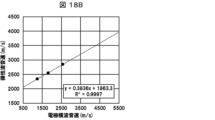
- FIG. 3 is a diagram showing a formula for calculating transverse wave sound speed. 3 is a graph showing the relationship between the transverse sound velocity of the electrode material and the center point CP of the electrode thickness in the results of Study Examples 1 to 3.
- 2 is a graph showing the relationship between the transverse wave sound velocity and the sound velocity (acoustic wave sound velocity) V of the electrode material in the results of Study Examples 1 to 3.
- 2 is a graph showing the relationship between the transverse sound velocity of the electrode material and the fractional bandwidth ⁇ f in the results of Study Examples 1 to 3.
- 12 is a table showing FEM simulation conditions regarding Al electrode thickness in study example 5.
- 12 is a graph showing FEM simulation results regarding the relationship between Al electrode thickness and fractional bandwidth ⁇ f in study example 5.
- 12 is a graph showing FEM simulation results regarding the relationship between Al electrode thickness and sound velocity V in study example 5.
- 12 is a table showing FEM simulation conditions regarding LN thickness in study example 5.
- 12 is a graph showing FEM simulation results regarding the relationship between LN thickness and fractional bandwidth ⁇ f in study example 5.
- 12 is a graph showing FEM simulation results regarding the relationship between LN thickness and sound velocity V in study example 5.
- 12 is a table showing FEM simulation conditions regarding LN cut angles in study example 5.
- 12 is a graph showing FEM simulation results regarding the relationship between the LN cut angle and the fractional bandwidth ⁇ f in Study Example 5.
- 12 is a graph showing FEM simulation results regarding the relationship between the LN cut angle and the sound velocity V in study example 5.
- 12 is a table showing FEM simulation conditions regarding LN propagation angle in study example 5.
- 12 is a graph showing FEM simulation results regarding the relationship between LN propagation angle and fractional bandwidth ⁇ f in study example 5.
- 12 is a graph showing FEM simulation results regarding the relationship between LN propagation angle and sound speed V in study example 5.
- 12 is a table showing FEM simulation conditions regarding Cu electrode thickness in Study Example 6.
- 12 is a graph showing FEM simulation results regarding the relationship between Cu electrode thickness and fractional bandwidth ⁇ f in Study Example 6.
- 12 is a graph showing FEM simulation results regarding the relationship between Cu electrode thickness and sound velocity V in study example 6.
- 12 is a table showing FEM simulation conditions regarding LN thickness in Study Example 6.
- 12 is a graph showing FEM simulation results regarding the relationship between LN thickness and fractional bandwidth ⁇ f in study example 6.
- 12 is a graph showing FEM simulation results regarding the relationship between LN thickness and sound velocity V in study example 6.
- 12 is a table showing FEM simulation conditions regarding LN cut angles in study example 6.
- 12 is a graph showing FEM simulation results regarding the relationship between the LN cut angle and the fractional bandwidth ⁇ f in study example 6.
- 12 is a graph showing FEM simulation results regarding the relationship between the LN cut angle and the sound velocity V in study example 6.
- 12 is a table showing FEM simulation conditions regarding LN propagation angle in study example 6.
- 12 is a graph showing FEM simulation results regarding the relationship between LN propagation angle and fractional bandwidth ⁇ f in study example 6.
- 12 is a graph showing FEM simulation results regarding the relationship between LN propagation angle and sound speed V in study example 6.
- 12 is a table showing FEM simulation conditions regarding Pt electrode thickness in Study Example 7.
- 12 is a graph showing FEM simulation results regarding the relationship between Pt electrode thickness and fractional bandwidth ⁇ f in Study Example 7.
- 12 is a graph showing FEM simulation results regarding the relationship between Pt electrode thickness and sound velocity V in study example 7.
- 12 is a table showing FEM simulation conditions regarding LN thickness in Study Example 7.
- 12 is a graph showing FEM simulation results regarding the relationship between LN thickness and fractional bandwidth ⁇ f in study example 7.
- 12 is a graph showing FEM simulation results regarding the relationship between LN thickness and sound velocity V in study example 7.
- 12 is a table showing FEM simulation conditions regarding LN cut angle in study example 7.
- 12 is a graph showing FEM simulation results regarding the relationship between the LN cut angle and the fractional bandwidth ⁇ f in study example 7.
- 12 is a graph showing FEM simulation results regarding the relationship between the LN cut angle and the sound velocity V in study example 7.
- 12 is a table showing FEM simulation conditions regarding LN propagation angle in study example 7.
- 12 is a graph showing FEM simulation results regarding the relationship between LN propagation angle and fractional bandwidth ⁇ f in study example 7.
- 12 is a graph showing FEM simulation results regarding the relationship between LN propagation angle and sound speed V in study example 7.
- 7 is a graph showing the relationship between the transverse sound velocity of the electrode material and the center point CP of the electrode thickness in the results of Study Examples 5 to 7.
- 7 is a graph showing the relationship between the transverse wave sound velocity and the sound velocity (elastic wave sound velocity) V of the electrode material in the results of Study Examples 5 to 7.
- 7 is a graph showing the relationship between the transverse sound velocity of the electrode material and the fractional bandwidth ⁇ f in the results of Study Examples 5 to 7.
- FIG. 3 is a perspective view showing another structural example of the elastic wave device according to an embodiment of the present disclosure.
- FIG. 3 is a cross-sectional view showing another configuration example of an elastic wave device according to an embodiment of the present disclosure.
- FIG. 3 is a cross-sectional view showing another configuration example of an elastic wave device according to an embodiment of the present disclosure.
- 1 is a diagram illustrating a schematic configuration of a communication device.
- the elastic wave device in this embodiment may optionally include known constituent members that are not shown in the respective figures referred to. Furthermore, the dimensions of the members in each figure do not faithfully represent the dimensions of the actual constituent members and the dimensional ratios of each member.
- FIG. 1 is a perspective view showing a configuration example of an elastic wave device 100 in this embodiment.
- FIG. 2 is a sectional view showing a configuration example of the elastic wave device 100 in this embodiment.
- the specific shape of the IDT electrode 3 included in the acoustic wave device 100 in this embodiment is not particularly limited, and the electrode fingers 32 of the IDT electrode 3 may be formed in various known shapes. Therefore, in FIG. 1, the electrode fingers 32 of the IDT electrode 3 are simply shown by diagonal hatching. Further, in FIG. 2 and the cross-sectional views referred to in the following description, for clarity of illustration, illustrations (cut-away cross-sectional views) are shown in which members on the back side of the cross-section are omitted.
- an elastic wave device 100 may include at least one resonator 1.
- the input terminal Tin and the output terminal Tout may be connected to the resonator 1.
- the resonator 1 may be configured as a frequency filter (SAW filter) that filters an electrical signal input to an input terminal Tin and outputs the filtered electrical signal to an output terminal Tout.
- SAW filter frequency filter
- the elastic wave device 100 may include a support substrate 5 , a piezoelectric layer 2 in direct or indirect contact with the support substrate 5 , and an IDT electrode 3 located on the piezoelectric layer 2 .
- the IDT electrode 3 is also called an excitation electrode.
- the elastic wave device 100 in this embodiment is configured to effectively excite an asymmetric zero-order moderam wave. This will be described in detail later.
- each of the plurality of resonators 1 may share the support substrate 5 and the piezoelectric layer 2.
- Each of the plurality of resonators 1 may have an individual IDT electrode 3.
- the support substrate 5 supports each part of the acoustic wave device 100.
- the specific material of the support substrate 5 is not particularly limited, and may be, for example, a Si substrate.
- the piezoelectric layer 2 may be made of a single crystal material having piezoelectricity.
- the material of the piezoelectric layer 2 may be lithium tantalate (also referred to as LiTaO 3 :LT) or lithium niobate (also referred to as LiNbO 3 :LN).
- the acoustic wave device 100 may include an intermediate layer 6 located between the support substrate 5 and the piezoelectric layer 2.
- the support substrate 5 and the piezoelectric layer 2 may be bonded to each other via an intermediate layer 6.
- the constituent material of the intermediate layer 6 may typically be silicon oxide (SiO x ).
- the intermediate layer 6 may be a SiO 2 film.
- the elastic wave device 100 does not need to have the intermediate layer 6.
- Acoustic wave device 100 with intermediate layer 6 may be easier to manufacture than acoustic wave device 100 without intermediate layer 6.
- the bonding layer formed between the support substrate 5 and the piezoelectric layer 2 by bonding them in the manufacturing process of the acoustic wave device 100 is The filter characteristics of device 100 may be adversely affected. This is because the distance between the bonding layer and the surface of the piezoelectric layer 2 on the side far from the support substrate 5 becomes relatively short.
- the IDT electrode 3 is typically an interdigitated electrode in which an electrode pair consisting of a first electrode finger 32a of a positive electrode and a second electrode finger 32b of a negative electrode is arranged periodically.
- the propagation direction of the SAW excited by the IDT electrode 3 is a direction perpendicular to the direction in which the first electrode finger 32a and the second electrode finger 32b extend.
- the propagation direction of the SAW propagating on the surface of the piezoelectric layer 2 is the x direction
- the thickness direction of each member of the acoustic wave device 100 is the z direction, which is orthogonal to the x direction and the z direction.
- the direction be the y direction.
- the positive direction in the z direction may be referred to as an upward direction
- the negative direction in the z direction may be referred to as a downward direction.
- the orthogonal coordinate system (xyz coordinate system) shown in FIG. 1 is appropriately shown in each drawing referred to in the following description.
- the IDT electrode 3 may have two bus bars 31 (a first bus bar 31a and a second bus bar 31b) facing each other in the y direction.
- the IDT electrode 3 may have a plurality of first electrode fingers 32a connected to the first bus bar 31a and a plurality of second electrode fingers 32b connected to the second bus bar 31b.
- the first electrode finger 32a may extend in the y direction from the first bus bar 31a toward the second bus bar 31b.
- the second electrode finger 32b may extend in the y direction from the second bus bar 31b toward the first bus bar 31a.
- the first electrode fingers 32a and the second electrode fingers 32b may be alternately and repeatedly positioned on the piezoelectric layer 2 at approximately constant intervals in the x direction.
- the first electrode finger 32a and the second electrode finger 32b may be collectively referred to as the electrode finger 32.
- the electrode finger pitch (pitch of electrode fingers) p in the IDT electrode 3 may be the distance between the centers of two adjacent electrode fingers 32 (in other words, the repetition interval of the electrode fingers 32) in the x direction.
- the length of one of the electrode fingers 32 (the first electrode finger 32a or the second electrode finger 32b) in the x direction is referred to as the width w.
- the first electrode finger 32a and the second electrode finger 32b may have the same or substantially the same width w.
- substantially the same means substantially the same, and means allowing for a difference (error) in dimensions of about ⁇ 5%. This also applies to the following description, and repeated explanation will be omitted.
- the width w may be set as appropriate, for example, depending on the electrical characteristics required of the elastic wave device 100.
- the width w may be set corresponding to the electrode finger pitch p.
- the ratio (w/p) of the width w to the electrode finger pitch p is referred to as duty.
- the width w and the electrode finger pitch p may be constant (that is, the duty is constant) over the entire electrode finger 32.
- constant is not limited to strictly no change, but is used in the sense of allowing an error of approximately ⁇ 5 degrees.
- the electrode finger 32 may have a thin flat plate shape extending in the y direction and made of a metal material, for example.
- the metal may be aluminum (Al), copper (Cu), or platinum (Pt).
- the structure (material and thickness) of the electrode finger 32 will be described in more detail later.
- the IDT electrode 3 may further include a protective layer covering the electrode fingers 32.
- the material of the protective layer may be, for example, SiO 2 , and any insulating material commonly used as a protective film may be used as appropriate.
- the elastic wave device 100 may include a pair of reflectors 4a and 4b corresponding to the IDT electrode 3.
- the reflectors 4a and 4b are also generically referred to as reflectors 4.
- the reflector 4 may be positioned to sandwich the IDT electrode 3 in the x direction.
- a relatively low frequency band for example, a frequency band of 700 MHz to 900 MHz (hereinafter, for convenience of explanation, may be referred to as a "target frequency band") is used for communication.
- the value calculated by dividing the bandwidth (pass band width) by the center frequency (resonant frequency) is called the fractional bandwidth (herein sometimes referred to as "fractional bandwidth ⁇ f").
- the fractional bandwidth ⁇ f the fractional bandwidth
- the minimum value is 1.1% in the downstream communication of Band 6. Therefore, the present inventors set the conditions required for the filter characteristics of the elastic wave device 100 to have a bandwidth in the target frequency band and have a fractional bandwidth ⁇ f of 1.1% or more.
- Lamb waves having a vibration plane perpendicular to the surface of the piezoelectric layer 2 are one type of various propagation modes in SAW, and are known to have multimodality.
- an asymmetric zero-order mode Lamb wave also referred to as an "A0 mode Lamb wave”
- “sonic velocity” is the propagation velocity of the elastic wave used in the elastic wave device 100, and can also be said to be the phase velocity.
- the present inventors came up with the idea of reducing the size of the elastic wave device 100 by lowering the sound velocity V using the A0 mode ram wave.
- the sound velocity V of the A0 mode ram wave decreases as the thickness of the piezoelectric layer 2 becomes thinner.
- the present inventors used finite element method (FEM) simulation to evaluate the relationship between the specific structure and filter characteristics of the elastic wave device 100 having the basic structure (bonded structure) described above. Then, the inventors discovered the conditions stipulated regarding the structure of the elastic wave device 100, and came up with the present invention.
- FEM finite element method
- FIG. 3 is a diagram showing an outline of an FEM simulation model of an elastic wave device.
- FIG. 4 is a table showing FEM simulation conditions.
- a piezoelectric layer 2 is bonded above a support substrate 5 via an intermediate layer 6, and a first It has an electrode finger 32a and a second electrode finger 32b.
- the material of the electrode fingers 32 was Al, Cu, or Pt.
- the material of the piezoelectric layer 2 was LT (LiTaO 3 ) or LN (LiNbO 3 ).
- the thickness of the electrode fingers 32, the thickness of the piezoelectric layer 2, the cut angle, and the propagation angle were used as variables. Further, in the FEM simulation, the electrode finger pitch p was fixed at 1.0 ⁇ m and the duty was fixed at 0.5.
- the wavelength ⁇ of the asymmetric zero-order mode ram wave is 2.0 ⁇ m, which is twice the electrode finger pitch p.
- the thickness of the intermediate layer 6 did not significantly affect the filter characteristics. Therefore, in the FEM simulation described below, the material of the intermediate layer 6 was SiO 2 and the thickness was fixed at 0.5 ⁇ as a general value.
- the Euler angles of the piezoelectric layer 2 can generally be expressed as ( ⁇ , ⁇ , ⁇ ). In the FEM simulation described below, ⁇ was fixed at 0°, and ⁇ and ⁇ were made variables. The meanings of ⁇ , ⁇ , and ⁇ in the Euler angle of the piezoelectric layer 2 can be understood based on common technical knowledge. For the sake of brevity, a detailed description of the Euler angle of the piezoelectric layer 2 will be omitted.
- the condition range required for each variable and the center point CP within that range were specified.
- the "center point CP" is not the median value of the range, but is a value selected in consideration of the balance of the characteristics of both the fractional bandwidth ⁇ f and the speed of sound V, and the reason for its selection is as follows. The individual FEM simulation results will be described later.
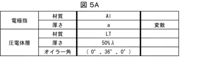
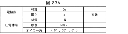
- FIG. 5A is a table showing FEM simulation conditions regarding the Al electrode thickness in Examination Example 1.
- FIG. 5B is a graph showing the FEM simulation results regarding the relationship between the Al electrode thickness and the fractional bandwidth ⁇ f in Examination Example 1.
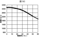
- FIG. 5C is a graph showing the FEM simulation results regarding the relationship between the Al electrode thickness and the sound velocity V in Study Example 1.
- the Euler angles of the piezoelectric layer 2 were fixed to common values (0°, 36°, 0°). Further, the LT thickness was fixed at 50% ⁇ .
- the fractional bandwidth ⁇ f is 1.1% fr or more when the Al electrode thickness is within the range of 0.6% ⁇ to 50.0% ⁇ .
- the maximum point in the fitting curve of the plot of the fractional bandwidth ⁇ f shown in FIG. 5B was selected as the center point CP. That is, the center point CP of the Al electrode thickness in Examination Example 1 was set to 30% ⁇ .
- the unit of the fractional bandwidth ⁇ f may be expressed as "%fr". This means that it is expressed as a percentage of the value calculated by dividing the passband width by the resonance frequency (fr).
- FIG. 6A is a table showing FEM simulation conditions regarding LT thickness in Study Example 1.
- FIG. 6B is a graph showing the FEM simulation results regarding the relationship between the LT thickness and the fractional bandwidth ⁇ f in Study Example 1.
- FIG. 6C is a graph showing the FEM simulation results regarding the relationship between the LT thickness and the sound velocity V in Study Example 1.
- the Euler angle of the piezoelectric layer 2 was fixed at the general values (0°, 36°, 0°)
- the Al electrode thickness was set using the above-mentioned FEM simulation. It was fixed at 30% ⁇ , which is the center point CP in the simulation results.
- the fractional bandwidth ⁇ f is 1.1%fr or more.
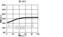
- the sound velocity V increases as the LT thickness increases, and the value of the sound velocity V becomes saturated when the LT thickness is 87.5% ⁇ .
- a point where the fractional bandwidth ⁇ f is relatively large and the speed of sound B is relatively slow was selected as the center point CP. That is, the center point CP of the LT thickness in Study Example 1 was set to 32.5% ⁇ .
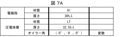
- FIG. 7A is a table showing FEM simulation conditions regarding the LT cut angle in Study Example 1.
- FIG. 7B is a graph showing the FEM simulation results regarding the relationship between the LT cut angle and the fractional bandwidth ⁇ f in Study Example 1.
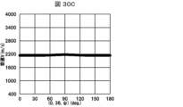
- FIG. 7C is a graph showing the FEM simulation results regarding the relationship between the LT cut angle and the sound speed V in Study Example 1.
- the Al electrode thickness was fixed at 30% ⁇ , which is the center point CP in the above FEM simulation results, and the LT thickness was fixed at the center point CP in the above FEM simulation results. It was fixed at a certain 32.5% ⁇ .
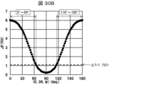
- the fractional bandwidth ⁇ f is 1.1% fr or more when the LT cut angle is in the range of 8° or more and 74° or less.
- the center point CP of the LT cut angle was set to 36°.
- FIG. 7B it can be seen that the center point CP of the LT cut angle is located near the maximum point in the fitting curve of the plot of the fractional bandwidth ⁇ f.
- FIG. 8A is a table showing FEM simulation conditions regarding the LT propagation angle in study example 1.
- FIG. 8B is a graph showing the FEM simulation results regarding the relationship between the LT propagation angle and the fractional bandwidth ⁇ f in Study Example 1.
- FIG. 8C is a graph showing the FEM simulation results regarding the relationship between the LT propagation angle and the sound speed V in Study Example 1.
- the Al electrode thickness was fixed at 30% ⁇ , which is the center point CP in the above-mentioned FEM simulation results.
- the LT thickness was fixed at 32.5% ⁇ , which is the center point CP in the above-mentioned FEM simulation results, and the LT cut angle was fixed at 36°.
- the fractional bandwidth is It can be seen that ⁇ f is 1.1%fr or more.
- the fitting curve of the plot of the fractional bandwidth ⁇ f shown in FIG. 8B actually has an upwardly convex peak because the LT propagation angles of 0° and 180° are equivalent.
- the maximum point of the fitting curve was selected as the center point CP. That is, the center point CP of the LT propagation angle was set to 0°.
- the main component of the constituent material of the piezoelectric layer 2 is lithium tantalate (LT), and the thickness is 20 mm. .0% ⁇ or more and 87.5% ⁇ or less. Furthermore, assuming the Euler angles of the piezoelectric layer 2 as ( ⁇ , ⁇ , ⁇ ), ⁇ is ⁇ 5° or more and 5° or less, ⁇ is 8° or more and 74° or less, and ⁇ is ⁇ 26° or more and 26° or less.
- the main component of the constituent material of the IDT electrode 3 is Al, and the thickness is 0.6% ⁇ or more and 50.0% ⁇ or less.
- the above ⁇ is the wavelength ⁇ of the A0 mode ram wave, and is defined as twice the length of the pitch p of the plurality of electrode fingers 32 included in the IDT electrode 3.
- the above definition of ⁇ is the same in the following description of this specification, and repeated description will be omitted.
- the Euler angle ⁇ of the piezoelectric layer 2 is defined in the range of ⁇ 5° or more and 5° or less from the viewpoint of allowing errors in the manufacturing process.
- the characteristics of the elastic wave device 100 hardly change in the range where ⁇ is ⁇ 5° or more and 5° or less.
- the resonator 1 can effectively excite or receive the A0 moderam wave.
- the elastic wave device 100 in configuration example 1 functions as a SAW filter that utilizes the A0 mode ram wave, and has frequency characteristics in which the fractional bandwidth ⁇ f is 1.1% fr or more.
- the sound velocity V of the conventional SAW is about 4000 m/s
- the sound velocity V of the A0 moderam wave is slower than that of the conventional SAW.
- the elastic wave device 100 having a certain resonant frequency with an elastic wave device (conventional elastic wave device) that uses a conventional SAW and has the same resonant frequency
- the resonator 1 can be downsized by using the A0 mode ram wave that propagates at a speed of sound V that is slower than that of the conventional SAW.
- the elastic wave device 100 can be effectively miniaturized while having frequency characteristics with a fractional bandwidth ⁇ f of 1.1% fr or more.
- the main component of the constituent material is component A
- the proportion of the component A to the entire constituent material is greater than 50% by mass. This also applies to the following description in this specification, and repeated description will be omitted.
- the piezoelectric layer 2 may be made of LT, or may be made substantially of LT.
- the IDT electrode 3 may be made of Al, or may be made substantially of Al.
- substantially consisting of component B means that the proportion of component B to the entire constituent material is 90% by mass or more. This also applies to the following description in this specification, and repeated description will be omitted.
- the piezoelectric layer 2 may contain LT in an amount of 70% by mass or more, or may contain LT in an amount of 80% by mass or more.
- the remainder of the constituent material of the piezoelectric layer 2 other than LT may consist of arbitrary additive components and unavoidable impurities.
- the IDT electrode 3 may contain Al at 70% by mass or more, or may contain Al at 80% by mass or more.
- the remainder of the constituent material of the IDT electrode 3 other than Al may consist of arbitrary additive components and unavoidable impurities.
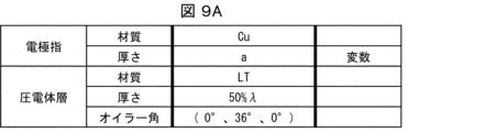
- FIG. 9A is a table showing FEM simulation conditions regarding the Cu electrode thickness in Examination Example 2.
- FIG. 9B is a graph showing the FEM simulation results regarding the relationship between the Cu electrode thickness and the fractional bandwidth ⁇ f in Examination Example 2.
- FIG. 9C is a graph showing the FEM simulation results regarding the relationship between the Cu electrode thickness and the sound velocity V in Examination Example 2.
- the Euler angles of the piezoelectric layer 2 were fixed to common values (0°, 36°, 0°).
- the fractional bandwidth ⁇ f is 1.1% fr or more when the Cu electrode thickness is in the range of 0.2% ⁇ to 50.0% ⁇ .
- the maximum point in the fitting curve of the plot of the fractional bandwidth ⁇ f shown in FIG. 9B was selected as the center point CP. That is, the center point CP of the Cu electrode thickness in Examination Example 2 was set to 20% ⁇ .
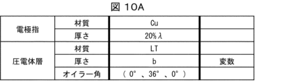
- FIG. 10A is a table showing FEM simulation conditions regarding LT thickness in Study Example 2.
- FIG. 10B is a graph showing the FEM simulation results regarding the relationship between the LT thickness and the fractional bandwidth ⁇ f in Study Example 2.
- FIG. 10C is a graph showing the FEM simulation results regarding the relationship between the LT thickness and the sound velocity V in Study Example 2.
- the Euler angle of the piezoelectric layer 2 was fixed at the common values (0°, 36°, 0°), and the Cu electrode thickness was It was fixed at 20% ⁇ , which is the center point CP in the simulation results.
- the fractional bandwidth ⁇ f is 1.1%fr or more.
- the sound velocity V increases as the LT thickness increases, and the value of the sound velocity V becomes saturated when the LT thickness is 90.0% ⁇ .
- a point where the fractional bandwidth ⁇ f is relatively large and the speed of sound B is relatively slow was selected as the center point CP. That is, the center point CP of the LT thickness in Examination Example 2 was set to 37.5% ⁇ .
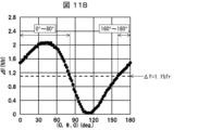
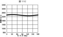
- FIG. 11A is a table showing FEM simulation conditions regarding the LT cut angle in study example 2.
- FIG. 11B is a graph showing the FEM simulation results regarding the relationship between the LT cut angle and the fractional bandwidth ⁇ f in study example 2.
- FIG. 11C is a graph showing the FEM simulation results regarding the relationship between the LT cut angle and the sound velocity V in study example 2.
- the Cu electrode thickness was fixed at 20% ⁇ , which is the center point CP in the above FEM simulation results, and the LT thickness was fixed at the center point CP in the above FEM simulation results. It was fixed at a certain 37.5% ⁇ .
- the fractional bandwidth is It can be seen that ⁇ f is 1.1%fr or more.
- the center point CP of the LT cut angle was set to 36°.
- FIG. 11B it can be seen that the center point CP of the LT cut angle is located near the maximum point in the fitting curve of the plot of the fractional bandwidth ⁇ f.
- FIG. 12A is a table showing FEM simulation conditions regarding the LT propagation angle in study example 2.
- FIG. 12B is a graph showing the FEM simulation results regarding the relationship between the LT propagation angle and the fractional bandwidth ⁇ f in study example 2.
- FIG. 12C is a graph showing the FEM simulation results regarding the relationship between the LT propagation angle and the sound speed V in study example 2.
- the Cu electrode thickness was fixed at 20% ⁇ , which is the center point CP in the above-mentioned FEM simulation results.
- the LT thickness was fixed at 37.5% ⁇ , which is the center point CP in the above-mentioned FEM simulation results, and the LT cut angle was fixed at 36°.
- the fractional bandwidth is It can be seen that ⁇ f is 1.1%fr or more.
- the fitting curve of the plot of the fractional bandwidth ⁇ f shown in FIG. 12B actually has an upwardly convex peak because the LT propagation angles of 0° and 180° are equivalent.
- the maximum point of the fitting curve was selected as the center point CP. That is, the center point CP of the LT propagation angle was set to 0°.
- the main component of the constituent material of the piezoelectric layer 2 is lithium tantalate (LT), and the thickness is 17 mm. .5% ⁇ or more and 90.0% ⁇ or less. Further, assuming the Euler angles of the piezoelectric layer 2 as ( ⁇ , ⁇ , ⁇ ), ⁇ is -5° or more and 5° or less, ⁇ is -20° or more and 80° or less, and ⁇ is -40° or more and 40° or less. .
- the main component of the constituent material of the IDT electrode 3 is Cu, and the thickness is 0.2% ⁇ or more and 58.0% ⁇ or less.
- the Euler angle ⁇ of the piezoelectric layer 2 is defined in the range of ⁇ 5° or more and 5° or less from the viewpoint of allowing errors in the manufacturing process.
- the piezoelectric layer 2 may be the same as in the first configuration example.
- the IDT electrode 3 may be made of Cu or may be made substantially of Cu.
- the IDT electrode 3 may contain 70% by mass or more of Cu, or may contain 80% by mass or more of Cu.
- the remainder of the constituent material of the IDT electrode 3 other than Cu may consist of arbitrary additive components and unavoidable impurities.
- the resonator 1 can effectively excite or receive the A0 mode ram wave.
- the resonator 1 can be downsized by using the A0 mode ram wave that propagates at a speed of sound V that is slower than that of the conventional SAW.
- the elastic wave device 100 can be effectively miniaturized while having frequency characteristics with a fractional bandwidth ⁇ f of 1.1% fr or more. This is the same in the following configuration examples 3 to 8, although a repeated explanation will be omitted.
- FIG. 13A is a table showing FEM simulation conditions regarding the Pt electrode thickness in Study Example 3.
- FIG. 13B is a graph showing the FEM simulation results regarding the relationship between the Pt electrode thickness and the fractional bandwidth ⁇ f in Study Example 3.
- FIG. 13C is a graph showing the FEM simulation results regarding the relationship between the Pt electrode thickness and the sound velocity V in Study Example 3.
- the Euler angles of the piezoelectric layer 2 were fixed to common values (0°, 36°, 0°).
- the fractional bandwidth ⁇ f is 1.1% fr or more when the Pt electrode thickness is within the range of 0.3% ⁇ to 74.0% ⁇ .
- the maximum point in the fitting curve of the plot of the fractional bandwidth ⁇ f shown in FIG. 13B was selected as the center point CP. That is, the center point CP of the Pt electrode thickness in Study Example 3 was set to 13% ⁇ .
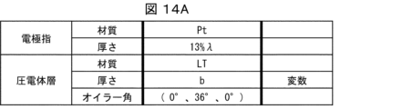
- FIG. 14A is a table showing FEM simulation conditions regarding LT thickness in Study Example 3.
- FIG. 14B is a graph showing the FEM simulation results regarding the relationship between the LT thickness and the fractional bandwidth ⁇ f in Study Example 3.
- FIG. 14C is a graph showing the FEM simulation results regarding the relationship between the LT thickness and the sound velocity V in Study Example 3.
- the Euler angle of the piezoelectric layer 2 was fixed at the general values (0°, 36°, 0°), and the Pt electrode thickness was It was fixed at 13% ⁇ , which is the center point CP in the simulation results.
- the fractional bandwidth ⁇ f is 1.1%fr or more.
- the sound velocity V increases as the LT thickness increases, and the value of the sound velocity V becomes saturated when the LT thickness is 85.0% ⁇ .
- a point where the fractional bandwidth ⁇ f is relatively large and the speed of sound B is relatively slow was selected as the center point CP. That is, the center point CP of the LT thickness in Study Example 3 was set to 40.0% ⁇ .
- FIG. 15A is a table showing FEM simulation conditions regarding the LT cut angle in study example 3.
- FIG. 15B is a graph showing the FEM simulation results regarding the relationship between the LT cut angle and the fractional bandwidth ⁇ f in Study Example 3.
- FIG. 15C is a graph showing the FEM simulation results regarding the relationship between the LT cut angle and the sound velocity V in Study Example 3.
- the Pt electrode thickness was fixed at 13% ⁇ , which is the center point CP in the above-mentioned FEM simulation results.
- the LT thickness was fixed at 40.0% ⁇ , which is the center point CP in the above-mentioned FEM simulation results.
- the fractional bandwidth is It can be seen that ⁇ f is 1.1%fr or more.
- the center point CP of the LT cut angle was set to 36°.
- FIG. 15B it can be seen that the center point CP of the LT cut angle is located near the maximum point in the fitting curve of the plot of the fractional bandwidth ⁇ f.
- FIG. 16A is a table showing FEM simulation conditions regarding the LT propagation angle in study example 3.
- FIG. 16B is a graph showing the FEM simulation results regarding the relationship between the LT propagation angle and the fractional bandwidth ⁇ f in Study Example 3.
- FIG. 16C is a graph showing the FEM simulation results regarding the relationship between the LT propagation angle and the sound speed V in Study Example 3.
- the Pt electrode thickness was fixed at 13% ⁇ , which is the center point CP in the above-mentioned FEM simulation results.
- the LT thickness was fixed at 40.0% ⁇ , which is the center point CP in the above-mentioned FEM simulation results, and the LT cut angle was fixed at 36°.
- the fractional bandwidth is It can be seen that ⁇ f is 1.1%fr or more.
- the fitting curve of the plot of the fractional bandwidth ⁇ f shown in FIG. 16B actually has an upwardly convex peak because the LT propagation angles of 0° and 180° are equivalent.
- the maximum point of the fitting curve was selected as the center point CP. That is, the center point CP of the LT propagation angle was set to 0°.
- the main component of the constituent material of the piezoelectric layer 2 is lithium tantalate (LT), and the thickness is 1.5 mm. .0% ⁇ or more and 85.0% ⁇ or less. Further, assuming the Euler angles of the piezoelectric layer 2 as ( ⁇ , ⁇ , ⁇ ), ⁇ is -5° or more and 5° or less, ⁇ is -40° or more and 86° or less, and ⁇ is -50° or more and 50° or less. .
- the main component of the constituent material of the IDT electrode 3 is Pt, and the thickness is 0.3% ⁇ or more and 74.0% ⁇ or less.
- the Euler angle ⁇ of the piezoelectric layer 2 is defined in the range of ⁇ 5° or more and 5° or less from the viewpoint of allowing errors in the manufacturing process.
- the piezoelectric layer 2 may be the same as in the configuration example 1 above.
- the IDT electrode 3 may be made of Pt or may be made substantially of Pt.
- the IDT electrode 3 may contain 70% by mass or more of Pt, or may contain 80% by mass or more of Pt.
- the remainder of the constituent material of the IDT electrode 3 other than Pt may consist of arbitrary additive components and unavoidable impurities.
- FIG. 17A is a table showing transverse sound speeds of major metal materials.
- FIG. 17B is a diagram showing a formula for calculating transverse wave sound speed.
- V is the transverse sound velocity (m/s)
- E is Young's modulus (Pa)
- ⁇ is the density (kg/m 3 )
- ⁇ is Poisson's ratio.
- the transverse sound velocities of Al, Cu, and Pt used in Study Examples 1 to 3 above are 2571 m/s, 1804 m/s, and 1244 m/s, respectively.
- the center point CP of the Al electrode thickness is 30% ⁇
- the sound velocity (acoustic wave sound speed) V at the center point CP is about 3000 m/s
- the fractional bandwidth at the center point CP is ⁇ f was approximately 1.6 (see Figures 5A-5C).
- the center point CP of the Cu electrode thickness is 20% ⁇
- the sound velocity (acoustic wave sound speed) V at the center point CP is about 2500 m/s
- the ratio at the center point CP is The bandwidth ⁇ f was approximately 2.1 (see FIGS. 9A-9C).
- the center point CP of the Pt electrode thickness is 13% ⁇
- the sound velocity (acoustic wave sound velocity) V at the center point CP is about 2300 m/s
- the fractional bandwidth at the center point CP is ⁇ f was approximately 2.5 (see FIGS. 13A-13C).
- FIG. 18A is a graph showing the relationship between the transverse sound velocity of the electrode material and the center point CP of the electrode thickness in the results of Study Examples 1 to 3.
- FIG. 18B is a graph showing the relationship between the transverse wave sonic velocity and the sonic velocity (acoustic wave sonic velocity) V of the electrode material in the results of Study Examples 1 to 3.
- FIG. 18C is a graph showing the relationship between the transverse sound velocity of the electrode material and the fractional bandwidth ⁇ f in the results of Study Examples 1 to 3.
- 18A to 18C show straight lines and determination coefficients calculated by approximating the plots corresponding to the results of Study Examples 1 to 3 using linear functions. As shown in FIGS. 18A to 18C, it can be seen that the transverse wave sonic velocity of the electrode material, the sonic velocity (acoustic wave sonic velocity) V, and the fractional bandwidth ⁇ f have a linear function relationship with each other.
- the fractional bandwidth ⁇ f is 1.1% fr or more.
- energy tends to concentrate around the electrode, and as a result, the fractional bandwidth ⁇ f tends to increase.
- Au had the lowest transverse wave sound velocity, which was 658 m/s. Based on this, the lower limit of the transverse sound velocity of the electrode material was set to 500 m/s.
- the main component of the constituent material of the piezoelectric layer 2 is lithium tantalate, and the thickness is The length is 15.0% ⁇ or more and 90.0% ⁇ or less. Further, assuming the Euler angles of the piezoelectric layer 2 as ( ⁇ , ⁇ , ⁇ ), ⁇ is -5° or more and 5° or less, ⁇ is -40° or more and 86° or less, and ⁇ is -50° or more and 50° or less. .
- the main component of the constituent material of the IDT electrode 3 is a metal having a transverse sound velocity of 500 m/s or more and 3473 m/s or less, and the thickness is 0.2% ⁇ or more and 74.0% ⁇ or less.
- the main component of the constituent material of the piezoelectric layer 2 is tantalum acid. It is lithium and has a thickness of 20.0% ⁇ or more and 85.0% ⁇ or less. Furthermore, assuming the Euler angles of the piezoelectric layer 2 as ( ⁇ , ⁇ , ⁇ ), ⁇ is ⁇ 5° or more and 5° or less, ⁇ is 8° or more and 74° or less, and ⁇ is ⁇ 26° or more and 26° or less.
- the main component of the constituent material of the IDT electrode 3 is a metal having a transverse sound velocity of 500 m/s or more and 3473 m/s or less, and the thickness is 0.6% ⁇ or more and 50.0% ⁇ or less.
- the piezoelectric layer 2 may be the same as in the first configuration example.
- the IDT electrode 3 may be made of a metal having a transverse sound velocity of 500 m/s or more and 3473 m/s or less (hereinafter referred to as "specific metal M1"), or may be substantially made of the specific metal M1.
- the main component of the constituent material may be the specific metal M1.
- the main component of the constituent material of the IDT electrode 3 may be specified depending on the electrode structure of the IDT electrode 3.
- the thickest layer among the plurality of layers constituting the laminated structure can have the material with the highest concentration as the main component.
- the average value of the transverse sound velocity of each material of the plurality of layers constituting the laminated structure may be regarded as the transverse sound velocity of the constituent material of the IDT electrode 3.
- the average value is, for example, 500 m/s or more and 3473 m/s. / May be within the following range. If the electrode has a laminated structure, the sound velocity can also be calculated, for example, based on a volume average.
- the electrode in the IDT electrode 3 may be made of an alloy.
- the material with the highest concentration in the alloy composition may be the main component.
- the concentration in the alloy composition can be measured using, for example, EDX (Energy Dispersive X-ray Spectroscopy) or WDX (Wavelength-Dispersive X-ray Spectroscopy).
- the transverse sound velocity of the constituent material of the IDT electrode 3 calculated based on the density, Young's modulus, and Poisson's ratio of the alloy may be within a range of, for example, 500 m/s or more and 3473 m/s or less. Poisson's ratio is, for example, 0.3 in various alloys.
- FIG. 19A is a table showing FEM simulation conditions regarding Al electrode thickness in Study Example 5.
- FIG. 19B is a graph showing the FEM simulation results regarding the relationship between the Al electrode thickness and the fractional bandwidth ⁇ f in Study Example 5.
- FIG. 19C is a graph showing the FEM simulation results regarding the relationship between the Al electrode thickness and the sound velocity V in Study Example 5.
- the Euler angles of the piezoelectric layer 2 were fixed to common values (0°, 36°, 0°).
- the fractional bandwidth ⁇ f is 1.1% fr or more within the range where the Al electrode thickness is 100% ⁇ or less.
- An Al electrode thickness exceeding 100% ⁇ is not realistic, and an Al electrode thickness that is too thin is also not realistic. Therefore, the range of the Al electrode thickness can be defined as 0.05% ⁇ or more and 100.0% ⁇ or less.
- the range of the Al electrode thickness is defined as 0.05% ⁇ or more and 50.0% ⁇ or less You may.
- the part of the maximum point in the fitting curve of the plot of the fractional bandwidth ⁇ f shown in FIG. 19B was selected as the center point CP. That is, the center point CP of the Al electrode thickness in Study Example 5 was set to 24% ⁇ .
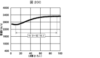
- FIG. 20A is a table showing FEM simulation conditions regarding LN thickness in Study Example 5.
- FIG. 20B is a graph showing FEM simulation results regarding the relationship between LN thickness and fractional bandwidth ⁇ f in Study Example 5.
- FIG. 20C is a graph showing the FEM simulation results regarding the relationship between LN thickness and sound velocity V in Study Example 5.
- the Euler angle of the piezoelectric layer 2 was fixed to the common values (0°, 36°, 0°)
- the Al electrode thickness was It was fixed at 24% ⁇ , which is the center point CP in the simulation results.
- the fractional bandwidth ⁇ f is 1.1%fr or more.
- the sound velocity V increases as the LN thickness increases, and the value of the sound velocity V becomes saturated when the LN thickness is 92.5% ⁇ .
- a point where the fractional bandwidth ⁇ f is relatively large and the speed of sound B is relatively slow was selected as the center point CP. That is, the center point CP of the LN thickness in Study Example 5 was set to 35.0% ⁇ .
- FIG. 21A is a table showing FEM simulation conditions regarding the LN cut angle in study example 5.
- FIG. 21B is a graph showing the FEM simulation results regarding the relationship between the LN cut angle and the fractional bandwidth ⁇ f in Study Example 5.
- FIG. 21C is a graph showing the FEM simulation results regarding the relationship between the LN cut angle and the sound speed V in Study Example 5.
- the Al electrode thickness was fixed at 24% ⁇ , which is the center point CP in the above FEM simulation results, and the LN thickness was fixed at the center point CP in the above FEM simulation results. It was fixed at a certain 35.0% ⁇ .
- the center point CP of the LN cut angle was set to 36°.
- FIG. 21B it can be seen that the center point CP of the LN cut angle is located near the maximum point in the fitting curve of the plot of the fractional bandwidth ⁇ f.
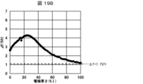
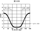
- FIG. 22A is a table showing FEM simulation conditions regarding the LN propagation angle in study example 5.
- FIG. 22B is a graph showing the FEM simulation results regarding the relationship between the LN propagation angle and the fractional bandwidth ⁇ f in Study Example 5.
- FIG. 22C is a graph showing the FEM simulation results regarding the relationship between the LN propagation angle and the sound speed V in Study Example 5.
- the Al electrode thickness was fixed at 24% ⁇ , which is the center point CP in the above-mentioned FEM simulation results.
- the LN thickness was fixed at 35.0% ⁇ , which is the center point CP in the above-mentioned FEM simulation results, and the LN cut angle was fixed at 36°.
- the fractional bandwidth is It can be seen that ⁇ f is 1.1%fr or more.
- the fitting curve of the plot of the fractional bandwidth ⁇ f shown in FIG. 22B actually has an upwardly convex peak because the LN propagation angles of 0° and 180° are equivalent.
- the maximum point of the fitting curve was selected as the center point CP. That is, the center point CP of the LN propagation angle was set to 0°.
- the main component of the constituent material of the piezoelectric layer 2 is lithium niobate, and the thickness is 10.0%. ⁇ or more and 92.5% ⁇ or less. Further, assuming the Euler angles of the piezoelectric layer 2 as ( ⁇ , ⁇ , ⁇ ), ⁇ is -5° or more and 5° or less, ⁇ is -38° or more and 90° or less, and ⁇ is -50° or more and 50° or less. .
- the main component of the constituent material of the IDT electrode 3 is Al, and the thickness is 0.05% ⁇ or more and 100.0% ⁇ or less.
- the piezoelectric layer 2 may be made of LN, or may be made substantially of LN.
- the piezoelectric layer 2 may contain 70% by mass or more of LN, or may contain 80% by mass or more of LN.
- the remainder of the constituent material of the piezoelectric layer 2 other than LN may consist of arbitrary additive components and unavoidable impurities.
- the IDT electrode 3 may be made of Al, or may be made substantially of Al.
- the IDT electrode 3 may contain 70% by mass or more of Al, or may contain 80% by mass or more of Al.
- the remainder of the constituent material of the IDT electrode 3 other than Al may consist of arbitrary additive components and unavoidable impurities.
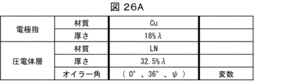
- FIG. 23A is a table showing FEM simulation conditions regarding Cu electrode thickness in Study Example 6.
- FIG. 23B is a graph showing the FEM simulation results regarding the relationship between the Cu electrode thickness and the fractional bandwidth ⁇ f in Study Example 6.
- FIG. 23C is a graph showing the FEM simulation results regarding the relationship between the Cu electrode thickness and the sound velocity V in Study Example 6.
- the Euler angles of the piezoelectric layer 2 were fixed to common values (0°, 36°, 0°).
- the range of the Cu electrode thickness can be defined as 0.05% ⁇ or more and 100.0% ⁇ or less.
- the range of the Cu electrode thickness is defined as 0.05% ⁇ or more and 66.0% ⁇ or less. You may.
- the part of the maximum point in the fitting curve of the plot of the fractional bandwidth ⁇ f shown in FIG. 23B was selected as the center point CP. That is, the center point CP of the Cu electrode thickness in Study Example 6 was set to 18% ⁇ .
- FIG. 24A is a table showing FEM simulation conditions regarding LN thickness in Study Example 6.
- FIG. 24B is a graph showing the FEM simulation results regarding the relationship between LN thickness and fractional bandwidth ⁇ f in Study Example 6.
- FIG. 24C is a graph showing the FEM simulation results regarding the relationship between LN thickness and sound velocity V in Study Example 6.
- the Euler angle of the piezoelectric layer 2 was fixed at the common values (0°, 36°, 0°), and the Cu electrode thickness was set using the above-mentioned FEM simulation. It was fixed at 18% ⁇ , which is the center point CP in the simulation results.
- the fractional bandwidth ⁇ f is 1.1%fr or more.
- the sound velocity V increases as the LN thickness increases, and the value of the sound velocity V becomes saturated when the LN thickness is 85.0% ⁇ .
- a point where the fractional bandwidth ⁇ f is relatively large and the speed of sound B is relatively slow was selected as the center point CP. That is, the center point CP of the LN thickness in Study Example 6 was set to 32.5% ⁇ .
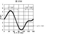
- FIG. 25A is a table showing FEM simulation conditions regarding the LN cut angle in study example 6.
- FIG. 25B is a graph showing the FEM simulation results regarding the relationship between the LN cut angle and the fractional bandwidth ⁇ f in Study Example 6.
- FIG. 25C is a graph showing the FEM simulation results regarding the relationship between the LN cut angle and the sound speed V in Study Example 6.
- the Cu electrode thickness was fixed at 18% ⁇ , which is the center point CP in the above FEM simulation results, and the LN thickness was fixed at the center point CP in the above FEM simulation results. It was fixed at a certain 32.5% ⁇ .
- the center point CP of the LN cut angle was set to 36°.
- FIG. 25B it can be seen that the center point CP of the LN cut angle is located near the maximum point in the fitting curve of the plot of the fractional bandwidth ⁇ f.
- FIG. 26A is a table showing FEM simulation conditions regarding the LN propagation angle in study example 6.
- FIG. 26B is a graph showing the FEM simulation results regarding the relationship between the LN propagation angle and the fractional bandwidth ⁇ f in Study Example 6.
- FIG. 26C is a graph showing the FEM simulation results regarding the relationship between the LN propagation angle and the sound speed V in Study Example 6.
- the Cu electrode thickness was fixed at 18% ⁇ , which is the center point CP in the above-mentioned FEM simulation results.
- the LN thickness was fixed at 32.5% ⁇ , which is the center point CP in the above-mentioned FEM simulation results, and the LN cut angle was fixed at 36°.
- the fractional bandwidth is It can be seen that ⁇ f is 1.1%fr or more.
- the fitting curve of the plot of the fractional bandwidth ⁇ f shown in FIG. 26B actually has an upwardly convex peak because the LN propagation angles of 0° and 180° are equivalent.
- the maximum point of the fitting curve was selected as the center point CP. That is, the center point CP of the LN propagation angle was set to 0°.
- the main component of the constituent material of the piezoelectric layer 2 is lithium niobate, and the thickness is 7.5% ⁇ or more 85. It is 0% ⁇ or less. Further, assuming the Euler angles of the piezoelectric layer 2 as ( ⁇ , ⁇ , ⁇ ), ⁇ is -5° or more and 5° or less, ⁇ is -52° or more and 84° or less, and ⁇ is -58° or more and 58° or less. .
- the main component of the constituent material of the IDT electrode 3 is Cu, and the thickness is 0.05% ⁇ or more and 100.0% ⁇ or less.
- the piezoelectric layer 2 may be the same as in configuration example 5 above.
- the IDT electrode 3 may be made of Cu or may be made substantially of Cu.
- the IDT electrode 3 may contain 70% by mass or more of Cu, or may contain 80% by mass or more of Cu.
- the remainder of the constituent material of the IDT electrode 3 other than Cu may consist of arbitrary additive components and unavoidable impurities.
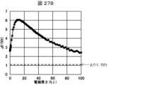
- FIG. 27A is a table showing FEM simulation conditions regarding Pt electrode thickness in Study Example 7.
- FIG. 27B is a graph showing the FEM simulation results regarding the relationship between the Pt electrode thickness and the fractional bandwidth ⁇ f in Study Example 7.
- FIG. 27C is a graph showing the FEM simulation results regarding the relationship between the Pt electrode thickness and the sound velocity V in Study Example 7.
- the Euler angles of the piezoelectric layer 2 were fixed to common values (0°, 36°, 0°).
- the fractional bandwidth ⁇ f is 1.1% fr or more within the range where the Pt electrode thickness is 100% ⁇ or less.
- a Pt electrode thickness exceeding 100% ⁇ is not realistic, and a Pt electrode thickness that is too thin is also not realistic. Therefore, the range of the Pt electrode thickness can be defined as 0.05% ⁇ or more and 100.0% ⁇ or less.
- the range of Pt electrode thickness is defined as 0.05% ⁇ or more and 86.0% ⁇ or less as the range in which the value of fractional bandwidth ⁇ f is equal to or greater than the value when the Pt electrode thickness is 0.05% ⁇ . You may.
- the part of the maximum point in the fitting curve of the plot of the fractional bandwidth ⁇ f shown in FIG. 27B was selected as the center point CP. That is, the center point CP of the Pt electrode thickness in Study Example 7 was set to 12% ⁇ .
- FIG. 28A is a table showing FEM simulation conditions regarding LN thickness in Study Example 7.
- FIG. 28B is a graph showing the FEM simulation results regarding the relationship between the LN thickness and the fractional bandwidth ⁇ f in Study Example 7.
- FIG. 28C is a graph showing the FEM simulation results regarding the relationship between LN thickness and sound velocity V in Study Example 7.
- the Euler angle of the piezoelectric layer 2 was fixed at the common values (0°, 36°, 0°)
- the Pt electrode thickness was It was fixed at 12% ⁇ , which is the center point CP in the simulation results.
- the fractional bandwidth ⁇ f is 1.1%fr or more.
- the sound velocity V increases as the LN thickness increases, and the value of the sound velocity V becomes saturated when the LN thickness is 82.5% ⁇ .
- a point where the fractional bandwidth ⁇ f is relatively large and the speed of sound B is relatively slow was selected as the center point CP. That is, the center point CP of the LN thickness in Study Example 7 was set to 32.5% ⁇ .
- FIG. 29A is a table showing FEM simulation conditions regarding the LN cut angle in Study Example 7.
- FIG. 29B is a graph showing the FEM simulation results regarding the relationship between the LN cut angle and the fractional bandwidth ⁇ f in Study Example 7.
- FIG. 29C is a graph showing the FEM simulation results regarding the relationship between the LN cut angle and the sound velocity V in Study Example 7.
- the Pt electrode thickness was fixed at 12% ⁇ , which is the center point CP in the above-mentioned FEM simulation results.
- the LN thickness was fixed at 32.5% ⁇ , which is the center point CP in the above-mentioned FEM simulation results.
- the center point CP of the LN cut angle was set to 36°.
- FIG. 29B it can be seen that the center point CP of the LN cut angle is located near the maximum point in the fitting curve of the plot of the fractional bandwidth ⁇ f.
- FIG. 30A is a table showing FEM simulation conditions regarding the LN propagation angle in study example 7.
- FIG. 30B is a graph showing the FEM simulation results regarding the relationship between the LN propagation angle and the fractional bandwidth ⁇ f in Study Example 7.
- FIG. 30C is a graph showing the FEM simulation results regarding the relationship between the LN propagation angle and the sound speed V in Study Example 7.
- the Pt electrode thickness was fixed at 12% ⁇ , which is the center point CP in the above-mentioned FEM simulation results.
- the LN thickness was fixed at 32.5% ⁇ , which is the center point CP in the above-mentioned FEM simulation results, and the LN cut angle was fixed at 36°.
- the fractional bandwidth is It can be seen that ⁇ f is 1.1%fr or more.
- the fitting curve of the plot of the fractional bandwidth ⁇ f shown in FIG. 30B actually has an upwardly convex peak because the LN propagation angles of 0° and 180° are equivalent.
- the maximum point of the fitting curve was selected as the center point CP. That is, the center point CP of the LN propagation angle was set to 0°.
- the main component of the constituent material of the piezoelectric layer 2 is lithium niobate, and the thickness is 7.5% ⁇ or more82. 5% ⁇ . Further, assuming the Euler angles of the piezoelectric layer 2 as ( ⁇ , ⁇ , ⁇ ), ⁇ is -5° or more and 5° or less, ⁇ is -58° or more and 86° or less, and ⁇ is -64° or more and 64° or less. .
- the main component of the constituent material of the IDT electrode 3 is Pt, and the thickness is 0.05% ⁇ or more and 100.0% ⁇ or less.
- the piezoelectric layer 2 may be the same as in the fifth configuration example.
- the IDT electrode 3 may be made of Pt or may be made substantially of Pt.
- the IDT electrode 3 may contain 70% by mass or more of Pt, or may contain 80% by mass or more of Pt.
- the remainder of the constituent material of the IDT electrode 3 other than Pt may consist of arbitrary additive components and unavoidable impurities.
- the center point CP of the Al electrode thickness is 24% ⁇
- the sound velocity (acoustic wave sound speed) V at the center point CP is about 3100 m/s
- the fractional bandwidth ⁇ f at the center point CP. was approximately 4.2 (see Figures 19A-19C).
- the center point CP of the Cu electrode thickness is 18% ⁇
- the sound velocity (acoustic wave sound speed) V at the center point CP is about 2600 m/s
- the specific band at the center point CP The width ⁇ f was approximately 5.3 (see FIGS. 23A-23C).
- the center point CP of the Pt electrode thickness is 12% ⁇
- the sound velocity (acoustic wave sound speed) V at the center point CP is about 2300 m/s
- the fractional bandwidth ⁇ f at the center point CP. was approximately 6.0 (see Figures 27A-27C).
- FIG. 31A is a graph showing the relationship between the transverse sound velocity of the electrode material and the center point CP of the electrode thickness in the results of Study Examples 5 to 7.
- FIG. 31B is a graph showing the relationship between the transverse wave sonic velocity and the sonic velocity (acoustic wave sonic velocity) V of the electrode material in the results of Study Examples 5 to 7.
- FIG. 31C is a graph showing the relationship between the transverse sound velocity of the electrode material and the fractional bandwidth ⁇ f in the results of Study Examples 5 to 7.
- 31A to 31C show straight lines and determination coefficients calculated by approximating the plots corresponding to the results of Study Examples 5 to 7 using linear functions. As shown in FIGS. 31A to 31C, it can be seen that the transverse wave sonic velocity of the electrode material, the sonic velocity (acoustic wave sonic velocity) V, and the fractional bandwidth ⁇ f have a linear function relationship with each other.
- the transverse sound velocity of the electrode material is about 5000 m/s or less, the fractional bandwidth ⁇ f becomes 1.1% fr or more.
- the sound speed of the conventional SAW is about 4000 m/s.
- Conventional SAW includes Rayleigh waves and leaky waves.
- the sound speed of leaky waves propagating through the LT film is approximately 4000 m/s. Therefore, as shown in FIG. 31B, the upper limit of the transverse wave sound speed of the electrode material was set to 4005 m/s as a range in which the sound speed (acoustic wave sound speed) V is slower than that of the conventional SAW. Further, as in Study Example 4 described above, the lower limit of the transverse sound velocity of the electrode material was set to 500 m/s.
- the main component of the constituent material of the piezoelectric layer 2 is lithium niobate, and the thickness is The value is 7.5% ⁇ or more and 92.5% ⁇ or less. Furthermore, assuming the Euler angles of the piezoelectric layer 2 as ( ⁇ , ⁇ , ⁇ ), ⁇ is -5° or more and 5° or less, ⁇ is -58° or more and 90° or less, and ⁇ is -64° or more and 64° or less. .
- the main component of the constituent material of the IDT electrode 3 is a metal having a transverse sound velocity of 500 m/s or more and 4005 m/s or less, and the thickness is 0.05% ⁇ or more and 100.0% ⁇ or less.
- the main component of the constituent material of the piezoelectric layer 2 is lithium niobate.
- the thickness is 10.0% ⁇ or more and 82.5% ⁇ or less.
- the Euler angles of the piezoelectric layer 2 as ( ⁇ , ⁇ , ⁇ ), ⁇ is -5° or more and 5° or less, ⁇ is -38° or more and 84° or less, and ⁇ is -50° or more and 50° or less.
- the main component of the constituent material of the IDT electrode 3 is a metal having a transverse sound velocity of 500 m/s or more and 4005 m/s or less, and the thickness is 0.05% ⁇ or more and 100.0% ⁇ or less.
- the piezoelectric layer 2 may be the same as the above structural example 5.
- the IDT electrode 3 may be made of a metal (hereinafter referred to as "specific metal M2") having a transverse sound velocity of 500 m/s or more and 4005 m/s or less, or may be substantially made of the specific metal M2.
- the main component of the constituent material may be the specific metal M2.
- the relationship between the constituent material of the IDT electrode 3 and the range of the transverse wave sound velocity is the same as that explained in connection with the above-mentioned configuration example 4, and therefore a repeated explanation will be omitted.
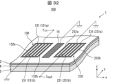
- FIG. 32 is a perspective view showing another structural example of the elastic wave device 100 in this embodiment.
- the elastic wave device 100 in this embodiment may be configured to excite an A0 mode ram wave, and the specific shape of the IDT electrode 3 is not particularly limited.
- the elastic wave device 100 may include a transversal type resonator 1.
- the resonator 1 includes a first IDT electrode 130 (input side IDT electrode) and a second IDT electrode 230 (output side IDT electrode) arranged in the X direction. It's fine.
- the first IDT electrode 130 may have two bus bars 131 (a first bus bar 131a and a second bus bar 131b) facing each other in the y direction.
- the second IDT electrode 230 may include two bus bars 231 (a first bus bar 231a and a second bus bar 231b) facing each other in the y direction.
- the input terminal Tin may be connected to the first bus bar 131a of the first IDT electrode 130
- the output terminal Tout may be connected to the second bus bar 231b of the second IDT electrode 230.
- the second bus bar 131b of the first IDT electrode 130 and the first bus bar 231a of the second IDT electrode 230 may each be connected to a ground terminal.
- the elastic wave device 100 may include the third electrode 14 in the propagation path between the first IDT electrode 130 and the second IDT electrode 230.
- the third electrode 14 may be, for example, an aluminum electrode film, and has a function of improving the propagation efficiency of the signal (A0 mode ram wave) from the first IDT electrode 130 to the second IDT electrode 230.
- the third electrode 14 may or may not be connected to the ground terminal. In the acoustic wave device 100, the third electrode 14 may not be provided.
- each of the first IDT electrode 130 and the second IDT electrode 230 only needs to have the same shape and component ratio as the above-described IDT electrode 3.
- the third electrode 14 a known configuration can be adopted.
- FIG. 33 is a sectional view showing another example of the configuration of the elastic wave device 100 in this embodiment.
- the resonator 1 included in the elastic wave device 100 may have an acoustic reflection film between the support substrate 5 and the piezoelectric layer 2.
- the specific structure of the acoustic reflective film is not particularly limited, for example, the acoustic wave device 100 may have a reflective multilayer film 60 between the support substrate 5 and the piezoelectric layer 2.
- the reflective multilayer film 60 may include a first layer 61 and a second layer 62 which are alternately laminated.
- the constituent material of the first layer 61 may have a lower acoustic impedance than the constituent material of the second layer 62.
- the main component of the first layer 61 may be silicon dioxide (SiO 2 ).
- the main component of the second layer 62 may be hafnium oxide (HfO 2 ).
- the main component of the second layer 62 is tantalum pentoxide (Ta 2 O 5 ), zirconium dioxide (ZrO 2 ), titanium oxide (TiO 2 ), or magnesium oxide (MgO). Good too.
- the reflective multilayer film 60 may include at least one first layer 61 and at least one second layer 62.
- the layer in the reflective multilayer film 60 that is in contact with the piezoelectric layer 2 is the first layer 61 .
- the layer closest to the support substrate 5 in the reflective multilayer film 60 may be either the first layer 61 or the second layer 62.
- the reflective multilayer film 60 may include a total of 3 or more and 12 or less layers, including the first layer 61 and the second layer 62.
- FIG. 34 is a sectional view showing another modification of the elastic wave device 100 in this embodiment.
- the resonator 1 included in the acoustic wave device 100 at least a portion of the IDT electrode 3 may be embedded in the piezoelectric layer 2.
- the upper surface of the electrode finger 32 and the upper surface of the piezoelectric layer 2 are aligned (flush), but the present invention is not limited thereto.
- the IDT electrode 3 may be embedded in the piezoelectric layer 2 such that the upper surface of the electrode finger 32 is convex or concave with respect to the upper surface of the piezoelectric layer 2. Thereby, spurious components can be effectively reduced.
- the resonance frequency of the elastic wave device 100 may be, for example, 700 MHz or more and 900 MHz or less.
- the resonance frequency can be adjusted by changing ⁇ (in other words, the electrode finger pitch p).
- ⁇ is set so that the desired resonance frequency is obtained, and the cross-sectional thicknesses (expressed in % ⁇ ) of the piezoelectric layer 2 and the IDT electrode 3 are calculated based on the set ⁇ .
- the resonator 1 having the piezoelectric layer 2 and the IDT electrode 3 having the calculated thickness may be manufactured.
- FIG. 35 is a diagram illustrating a schematic configuration of the communication device 151.
- the communication device 151 is an application example of the elastic wave device 100 according to one aspect of the present disclosure, and performs wireless communication using radio waves.
- the communication device 151 may include one duplexer 101 as a transmission filter 109 and another duplexer 101 as a reception filter 111.
- Each of the two duplexers 101 may include the elastic wave device 100 according to one aspect of the present disclosure. In this way, the communication device 151 may include the elastic wave device 100 according to one aspect of the present disclosure.
- a transmission information signal TIS containing information to be transmitted is modulated and frequency-increased (converted to a high-frequency signal having a carrier frequency) by an RF-IC (Radio Frequency-Integrated Circuit) 153, and the transmission information signal TIS is converted into a transmission signal. It may be converted to TS.
- the bandpass filter 155 may remove unnecessary components other than the transmission passband for the TS.
- the TS after removing unnecessary components may be amplified by the amplifier 157 and input to the transmission filter 109.
- the transmission filter 109 may remove unnecessary components outside the transmission passband from the input transmission signal TS.
- the transmission filter 109 may output the TS from which unnecessary components have been removed to the antenna 159 via the antenna terminal.
- the antenna 159 may convert the TS, which is an electrical signal input to itself, into a radio wave as a wireless signal, and transmit the radio wave to the outside of the communication device 151.
- the antenna 159 may convert the received radio waves from the outside into a reception signal RS, which is an electrical signal, and input the RS to the reception filter 111 via the antenna terminal.
- the reception filter 111 may remove unnecessary components other than the reception passband from the input RS.
- the reception filter 111 may output the reception signal RS from which unnecessary components have been removed to the amplifier 161.
- the output RS may be amplified by the amplifier 161.
- the bandpass filter 163 may remove unnecessary components other than the receiving passband from the amplified RS.
- the frequency of the RS after unnecessary component removal is lowered and demodulated by the RF-IC 153, and may be converted into a received information signal RIS.
- the TIS and RIS may be low frequency signals (baseband signals) containing appropriate information.
- TIS and RIS may be analog audio signals or digitized audio signals.
- the passband of the wireless signal may be set as appropriate and may conform to various known standards.
Abstract
弾性波装置を小型化する。弾性波装置は、支持基板と、支持基板に直接的又は間接的に接する圧電体層と、圧電体層上に位置するIDT電極と、を有し、非対称0次モードラム波を励振する。
Description
本開示は、弾性波装置および通信装置に関する。
従来、圧電結晶上にIDT(Interdigital Transducer)電極を形成した構造を有する弾性波素子が知られている。弾性波素子は、例えば、特定の周波数近傍の弾性表面波(SAW:Surface Acoustic Wave)の励振および特定の周波数近傍の電気信号の受信を行うフィルタ(SAWフィルタ)として用いることができ、通信機器におけるバンドパスフィルタ等に使用されている(例えば、特許文献1を参照)。
本開示の一態様に係る弾性波装置は、支持基板と、前記支持基板に直接的又は間接的に接する圧電体層と、前記圧電体層上に位置するIDT電極と、を有し、非対称0次モードラム波を励振する。
以下、本開示の一例である実施形態の弾性波装置について、図面を参照して詳細に説明する。但し、以下の記載は発明の趣旨をより良く理解させるためのものであり、特に指定のない限り、本開示を限定するものではない。本明細書において特記しない限り、数値範囲を表す「A~B」は、「A以上B以下」を意味する。また、以下の説明において参照する各図は、説明の便宜上、実施形態を説明する上で必要な主要部材のみを簡略化して示したものであり、公知の技術的事項については、簡潔化のために説明を適宜省略する。よって、本実施形態における弾性波装置は、参照する各図に示されていない公知の構成部材を任意に備えていてよい。また、各図中の部材の寸法は、実際の構成部材の寸法および各部材の寸法比率等を忠実に表したものではない。
<弾性波装置の構成の概略>
図1は、本実施形態における弾性波装置100の構成例を示す斜視図である。図2は本実施形態における弾性波装置100の構成例を示す断面図である。本実施形態における弾性波装置100の有するIDT電極3の具体的な形状は特に限定されず、IDT電極3の電極指32は、公知の各種形状に形成されていてよい。それゆえ、図1においてIDT電極3の電極指32を単に斜線ハッチングにて図示している。また、図2および以下の説明で参照する断面図においては、図示の平明化のために、断面よりも奥側の部材の図示を省略した図(切断部断面図)を示している。
図1は、本実施形態における弾性波装置100の構成例を示す斜視図である。図2は本実施形態における弾性波装置100の構成例を示す断面図である。本実施形態における弾性波装置100の有するIDT電極3の具体的な形状は特に限定されず、IDT電極3の電極指32は、公知の各種形状に形成されていてよい。それゆえ、図1においてIDT電極3の電極指32を単に斜線ハッチングにて図示している。また、図2および以下の説明で参照する断面図においては、図示の平明化のために、断面よりも奥側の部材の図示を省略した図(切断部断面図)を示している。
図1および図2に示すように、本開示の一態様における弾性波装置100は、少なくとも1つの共振子1を有していてよい。一例における弾性波装置100では、入力端子Tinおよび出力端子Toutが共振子1に接続されていてよい。共振子1は、入力端子Tinに入力された電気信号をフィルタリングし、フィルタリング後の電気信号を出力端子Toutに出力する周波数フィルタ(SAWフィルタ)として構成されてよい。
弾性波装置100は、支持基板5と、支持基板5に直接的又は間接的に接する圧電体層2と、圧電体層2上に位置するIDT電極3と、を有していてよい。IDT電極3は、励振電極とも称される。そして、本実施形態における弾性波装置100は、非対称0次モードラム波を効果的に励振するように構成されている。このことについて、詳しくは後述する。
弾性波装置100に複数の共振子1が含まれる場合、複数の共振子1のそれぞれは、支持基板5と圧電体層2とを共有していてよい。複数の共振子1のそれぞれは、個別のIDT電極3を有していてよい。
支持基板5は、弾性波装置100の各部を支持する。支持基板5は、その具体的な材質は特に限定されず、例えば、Si基板であってよい。
圧電体層2は、圧電性を有する単結晶材料によって構成されてよい。例えば、圧電体層2の材料は、タンタル酸リチウム(LiTaO3:LTとも称される)またはニオブ酸リチウム(LiNbO3:LNとも称される)であってよい。
弾性波装置100は、支持基板5と圧電体層2との間に位置する中間層6を有していてよい。支持基板5と圧電体層2とは、中間層6を介して接合されていてよい。中間層6の構成材料は、典型的には酸化シリコン(SiOx)であってよい。一例として、中間層6は、SiO2膜であってよい。弾性波装置100は、中間層6を有していなくてもよい。中間層6を有する弾性波装置100は、中間層6を有しない弾性波装置100よりも製造が容易であり得る。また、弾性波装置100が中間層6を有しない場合、弾性波装置100の製造過程において支持基板5と圧電体層2とを接合することによりそれらの間に形成される接合層が、弾性波装置100のフィルタ特性に悪影響を及ぼし得る。これは、当該接合層と、圧電体層2における支持基板5から遠い側の表面と、の距離が比較的近くなるためである。
IDT電極3は、典型的には、正極の第1電極指32aと、負極の第2電極指32bとからなる電極対を周期的に配置した、交差指状電極である。圧電体層2の表面において、IDT電極3によって励振されるSAWの伝搬方向は、第1電極指32aおよび第2電極指32bがそれぞれ延びる方向に直交する方向である。
図1では、弾性波装置100における、圧電体層2の表面を伝搬するSAWの伝搬方向をx方向、弾性波装置100の各部材の厚さ方向をz方向、x方向およびz方向に直交する方向をy方向とする。以下では、z方向の正の向きを上方向、z方向の負の向きを下方向と称することがある。また、以下の説明において参照する各図面に、図1に示されている直交座標系(xyz座標系)を適宜示している。
IDT電極3は、y方向において互いに対向している2本のバスバー31(第1バスバー31aおよび第2バスバー31b)を有していてよい。IDT電極3は、第1バスバー31aに接続された複数の第1電極指32aと、第2バスバー31bに接続された複数の第2電極指32bと、を有していてよい。第1電極指32aは、第1バスバー31aから第2バスバー31bに向かってy方向に延びていてよい。第2電極指32bは、第2バスバー31bから第1バスバー31aに向かってy方向に延びていてよい。
図2を参照して、第1電極指32aおよび第2電極指32bは、圧電体層2上において、x方向に概ね一定の間隔を有するように、交互に繰り返して位置していてよい。本明細書では、第1電極指32aおよび第2電極指32bを、電極指32と総称することがある。IDT電極3における電極指ピッチ(電極指のピッチ)pは、x方向において、隣り合う2つの電極指32の中心間の距離(換言すれば電極指32の繰り返し間隔)であってよい。一般に、IDT電極3によって励振されるSAWの波長λは、電極指ピッチpの2倍の長さとして規定されてよい。以下では、λ=2pと規定する。
また、本明細書において、電極指32(第1電極指32aまたは第2電極指32b)のうちの1本のx方向における長さを幅wと称する。第1電極指32aおよび第2電極指32bは、互いに同一または略同一の幅wを有していてよい。本明細書において、「略同一」とは、実質的に同一であることを意味し、±5%程度の寸法の相違(誤差)を許容することを意味する。このことは、以下の記載においても同じであり、繰り返して説明することは省略する。
幅wは、例えば、弾性波装置100に要求される電気特性に応じて適宜設定されてよい。一例として、幅wは、電極指ピッチpに対応して設定されてよい。本明細書では、電極指ピッチpに対する幅wの比率(w/p)を、Duty(デューティ)と称する。共振子1は、電極指32の全体において幅wおよび電極指ピッチpが一定(すなわちデューティが一定)であってよい。本明細書において、「一定である」とは、厳密に変化が無いことに限るものでなく、±5度程度の誤差を許容する意味で用いる。
電極指32は、例えば、金属材料により形成された、y方向に延びる薄厚の平板状であってよい。一例として、当該金属は、アルミニウム(Al)、銅(Cu)、または白金(Pt)であってよい。電極指32の構成(材質および厚さ)について、より詳しくは後述する。
IDT電極3は、電極指32を覆う保護層をさらに含んでいてもよい。当該保護層の材料は、例えばSiO2であってよく、一般的に保護膜として用いられる絶縁材料が適宜用いられてよい。
弾性波装置100は、IDT電極3に対応する一対の反射器4a・4bを有していてもよい。本明細書では、反射器4a・4bを、総称的に反射器4とも称する。反射器4は、x方向においてIDT電極3を挟むように位置してよい。
<本開示の知見の概要>
通信機器等において、比較的低い周波数の帯域であって、例えば700MHz~900MHzの周波数帯(以下、説明の便宜上、「目的周波数帯」と称することがある)が通信に用いられる。帯域幅(通過帯域幅)を中心周波数(共振周波数)で割ることにより算出される値は、比帯域幅(本明細書において、「比帯域幅Δf」と称することがある)と呼ばれる。目的周波数帯を利用する現行の各種の通信バンドのそれぞれの比帯域幅Δfのうち、最小の値は、Band6の下り方向通信における1.1%である。そこで、本発明者らは、弾性波装置100のフィルタ特性に要求される条件として、目的周波数帯に帯域幅を有し、かつ比帯域幅Δfが1.1%以上であることを設定した。
通信機器等において、比較的低い周波数の帯域であって、例えば700MHz~900MHzの周波数帯(以下、説明の便宜上、「目的周波数帯」と称することがある)が通信に用いられる。帯域幅(通過帯域幅)を中心周波数(共振周波数)で割ることにより算出される値は、比帯域幅(本明細書において、「比帯域幅Δf」と称することがある)と呼ばれる。目的周波数帯を利用する現行の各種の通信バンドのそれぞれの比帯域幅Δfのうち、最小の値は、Band6の下り方向通信における1.1%である。そこで、本発明者らは、弾性波装置100のフィルタ特性に要求される条件として、目的周波数帯に帯域幅を有し、かつ比帯域幅Δfが1.1%以上であることを設定した。
また、上記の目的周波数帯を利用する通信機器等に搭載される弾性波装置100について、更なる小型化が要求される。ここで、一般に、圧電体層2の表面に対して垂直な振動面を有するラム波は、SAWにおける各種の伝搬モードのうちの1種であり、多モード性を有することが知られている。ラム波のうち、非対称0次モードラム波(「A0モードラム波」とも称される)は、一般的な各種のSAWよりも音速が低い。本明細書において、「音速」は、弾性波装置100において利用する弾性波の伝搬速度であり、位相速度とも言える。
本発明者らは、A0モードラム波を利用して音速Vを低下させることにより、弾性波装置100の小型化を実現することを着想した。A0モードラム波は、圧電体層2の厚さを薄くするにつれて音速Vが低くなる。しかし、A0モードラム波を利用して、目的周波数帯における比帯域幅Δfが1.1%以上の条件を満たす弾性波装置100については知られておらず、弾性波装置100に要求される具体的な条件は明らかでない。
本発明者らは、上述した基本構造(貼り合わせ構造)を有する弾性波装置100について、有限要素法(FEM)シミュレーションを用いて、具体的な構造とフィルタ特性との関係を評価した。そして、弾性波装置100の構造に関して規定される条件を見出し、本願発明を想到した。以下、FEMシミュレーションを用いて本発明者らが探索した結果、すなわち、比帯域幅Δfおよび音速Vの特性が所定の条件を満たす、弾性波装置100における共振子1の構造について説明する。
<FEMシミュレーションの基本構造>
図3は、弾性波装置のFEMシミュレーションモデルの概要を示す図である。図4は、FEMシミュレーション条件について示す表である。図3に示すように、弾性波装置のFEMシミュレーションモデルSMは、支持基板5の上方に中間層6を介して圧電体層2が接合されており、圧電体層2の表面に位置する第1電極指32aおよび第2電極指32bを有している。
図3は、弾性波装置のFEMシミュレーションモデルの概要を示す図である。図4は、FEMシミュレーション条件について示す表である。図3に示すように、弾性波装置のFEMシミュレーションモデルSMは、支持基板5の上方に中間層6を介して圧電体層2が接合されており、圧電体層2の表面に位置する第1電極指32aおよび第2電極指32bを有している。
図4に示すような条件にてFEMシミュレーションを行った。電極指32の材質は、Al、Cu、またはPtとした。圧電体層2の材質は、LT(LiTaO3)またはLN(LiNbO3)とした。電極指32の厚さ、並びに、圧電体層2の厚さ、カット角、および伝搬角を変数とした。また、FEMシミュレーションにおいて、電極指ピッチpは1.0μm、デューティは0.5に固定した。非対称0次モードラム波の波長λは、電極指ピッチpの2倍の2.0μmとなる。
ここで、予備的なFEMシミュレーションにおいて、中間層6の厚さは、フィルタ特性に大きく影響しなかった。そのため、以下に説明するFEMシミュレーションにおいて、中間層6の材質はSiO2とし、厚さは一般的な値として0.5λに固定した。
圧電体層2のオイラー角は、一般に(φ、θ、ψ)と表すことができる。以下に説明するFEMシミュレーションでは、φは0°に固定し、θおよびψを変数とした。圧電体層2のオイラー角におけるφ、θ、およびψのそれぞれの意味は、技術常識に基づいて理解することができる。簡潔化のために、圧電体層2のオイラー角について詳細に説明することは省略する。
以下に説明する複数のFEMシミュレーション結果のそれぞれにおいて、各変数について求められる条件範囲、および、その範囲内における中心点CPを特定した。本明細書において、「中心点CP」とは、範囲の中央値ではなく、比帯域幅Δfおよび音速Vの両方の特性のバランスを考慮して選択された値であり、その選択理由については、個々のFEMシミュレーション結果にて後述する。
<検討例1:LT膜・Al電極>
検討例1では、電極材料をAlとし、圧電体層2をLT膜としてFEMシミュレーションを行った。
検討例1では、電極材料をAlとし、圧電体層2をLT膜としてFEMシミュレーションを行った。
(Al電極厚さ)
図5Aは、検討例1における、Al電極厚さに関するFEMシミュレーション条件について示す表である。図5Bは、検討例1における、Al電極厚さと比帯域幅Δfとの関係についてのFEMシミュレーション結果を示すグラフである。図5Cは、検討例1における、Al電極厚さと音速Vとの関係についてのFEMシミュレーション結果を示すグラフである。検討例1における、Al電極厚さに関するFEMシミュレーションでは、圧電体層2のオイラー角を、一般的な値である(0°、36°、0°)に固定した。また、LT厚さを50%λに固定した。
図5Aは、検討例1における、Al電極厚さに関するFEMシミュレーション条件について示す表である。図5Bは、検討例1における、Al電極厚さと比帯域幅Δfとの関係についてのFEMシミュレーション結果を示すグラフである。図5Cは、検討例1における、Al電極厚さと音速Vとの関係についてのFEMシミュレーション結果を示すグラフである。検討例1における、Al電極厚さに関するFEMシミュレーションでは、圧電体層2のオイラー角を、一般的な値である(0°、36°、0°)に固定した。また、LT厚さを50%λに固定した。
図5A~5Cに示すように、Al電極厚さが0.6%λ以上50.0%λ以下の範囲内において、比帯域幅Δfが1.1%fr以上となることがわかる。音速VとAl電極厚さとの関係については、概して、Al電極厚さが大きいほど音速Vが小さくなる傾向にあることがわかる。図5Bに示す比帯域幅Δfのプロットのフィッティングカーブにおける極大点の部分を中心点CPとして選択した。すなわち、検討例1におけるAl電極厚さの中心点CPは、30%λとした。
本明細書において、比帯域幅Δfの単位を「%fr」と示すことがある。これは、通過帯域幅を共振周波数(fr)で割って算出された値の百分率表記であることを意味する。
(LT厚さ)
図6Aは、検討例1における、LT厚さに関するFEMシミュレーション条件について示す表である。図6Bは、検討例1における、LT厚さと比帯域幅Δfとの関係についてのFEMシミュレーション結果を示すグラフである。図6Cは、検討例1における、LT厚さと音速Vとの関係についてのFEMシミュレーション結果を示すグラフである。検討例1における、LT厚さに関するFEMシミュレーションでは、圧電体層2のオイラー角を、一般的な値である(0°、36°、0°)に固定し、Al電極厚さを上述のFEMシミュレーション結果における中心点CPである30%λに固定した。
図6Aは、検討例1における、LT厚さに関するFEMシミュレーション条件について示す表である。図6Bは、検討例1における、LT厚さと比帯域幅Δfとの関係についてのFEMシミュレーション結果を示すグラフである。図6Cは、検討例1における、LT厚さと音速Vとの関係についてのFEMシミュレーション結果を示すグラフである。検討例1における、LT厚さに関するFEMシミュレーションでは、圧電体層2のオイラー角を、一般的な値である(0°、36°、0°)に固定し、Al電極厚さを上述のFEMシミュレーション結果における中心点CPである30%λに固定した。
図6A~6Cに示すように、LT厚さが20.0%λ以上の範囲において、比帯域幅Δfが1.1%fr以上となることがわかる。また、LT厚さが20.0%λ以上の範囲において、LT厚さを大きくするにつれて音速Vが大きくなり、LT厚さが87.5%λで音速Vの値が飽和した。この結果に基づいて、比帯域幅Δfが比較的大きく、音速Bが比較的遅い点を中心点CPとして選択した。すなわち、検討例1におけるLT厚さの中心点CPは、32.5%λとした。
(LTカット角)
図7Aは、検討例1における、LTカット角に関するFEMシミュレーション条件について示す表である。図7Bは、検討例1における、LTカット角と比帯域幅Δfとの関係についてのFEMシミュレーション結果を示すグラフである。図7Cは、検討例1における、LTカット角と音速Vとの関係についてのFEMシミュレーション結果を示すグラフである。検討例1における、LTカット角に関するFEMシミュレーションでは、Al電極厚さを上述のFEMシミュレーション結果における中心点CPである30%λに固定し、LT厚さを上述のFEMシミュレーション結果における中心点CPである32.5%λに固定した。
図7Aは、検討例1における、LTカット角に関するFEMシミュレーション条件について示す表である。図7Bは、検討例1における、LTカット角と比帯域幅Δfとの関係についてのFEMシミュレーション結果を示すグラフである。図7Cは、検討例1における、LTカット角と音速Vとの関係についてのFEMシミュレーション結果を示すグラフである。検討例1における、LTカット角に関するFEMシミュレーションでは、Al電極厚さを上述のFEMシミュレーション結果における中心点CPである30%λに固定し、LT厚さを上述のFEMシミュレーション結果における中心点CPである32.5%λに固定した。
図7A~7Cに示すように、LTカット角が8°以上74°以下の範囲において、比帯域幅Δfが1.1%fr以上となることがわかる。他のFEMシミュレーションにおける探索との統一のために、LTカット角の中心点CPは、36°とした。図7Bに示すように、上記LTカット角の中心点CPは、比帯域幅Δfのプロットのフィッティングカーブにおける極大点の近傍に位置することがわかる。
(LT伝搬角)
図8Aは、検討例1における、LT伝搬角に関するFEMシミュレーション条件について示す表である。図8Bは、検討例1における、LT伝搬角と比帯域幅Δfとの関係についてのFEMシミュレーション結果を示すグラフである。図8Cは、検討例1における、LT伝搬角と音速Vとの関係についてのFEMシミュレーション結果を示すグラフである。検討例1における、LT伝搬角に関するFEMシミュレーションでは、Al電極厚さを上述のFEMシミュレーション結果における中心点CPである30%λに固定した。また、LT厚さを上述のFEMシミュレーション結果における中心点CPである32.5%λに固定し、LTカット角を36°に固定した。
図8Aは、検討例1における、LT伝搬角に関するFEMシミュレーション条件について示す表である。図8Bは、検討例1における、LT伝搬角と比帯域幅Δfとの関係についてのFEMシミュレーション結果を示すグラフである。図8Cは、検討例1における、LT伝搬角と音速Vとの関係についてのFEMシミュレーション結果を示すグラフである。検討例1における、LT伝搬角に関するFEMシミュレーションでは、Al電極厚さを上述のFEMシミュレーション結果における中心点CPである30%λに固定した。また、LT厚さを上述のFEMシミュレーション結果における中心点CPである32.5%λに固定し、LTカット角を36°に固定した。
図8A~8Cに示すように、LT伝搬角が0°以上26°以下および154°以上180°以下の範囲、換言すればLT伝搬角が-26°以上26°以下の範囲において、比帯域幅Δfが1.1%fr以上となることがわかる。図8Bに示す比帯域幅Δfのプロットのフィッティングカーブには、LT伝搬角の0°と180°とは等価であるために、実際上、上に凸のピークが存在する。当該フィッティングカーブの極大点の部分を中心点CPとして選択した。すなわち、LT伝搬角の中心点CPは、0°とした。
<構成例1>
上述の検討例1のFEMシミュレーション結果に基づく、本実施形態の構成例1における弾性波装置100では、圧電体層2の構成材料の主成分がタンタル酸リチウム(LT)であり、厚さが20.0%λ以上87.5%λ以下である。また、圧電体層2のオイラー角を(φ、θ、ψ)として、φが-5°以上5°以下、θが8°以上74°以下、ψが-26°以上26°以下である。IDT電極3の構成材料の主成分がAlであり、厚さが0.6%λ以上50.0%λ以下である。上記λは、A0モードラム波の波長λであり、IDT電極3に含まれる複数の電極指32のピッチpの2倍の長さとして規定される。上記λの定義については、本明細書における以下の説明においても同じであり、繰り返して記載することは省略する。
上述の検討例1のFEMシミュレーション結果に基づく、本実施形態の構成例1における弾性波装置100では、圧電体層2の構成材料の主成分がタンタル酸リチウム(LT)であり、厚さが20.0%λ以上87.5%λ以下である。また、圧電体層2のオイラー角を(φ、θ、ψ)として、φが-5°以上5°以下、θが8°以上74°以下、ψが-26°以上26°以下である。IDT電極3の構成材料の主成分がAlであり、厚さが0.6%λ以上50.0%λ以下である。上記λは、A0モードラム波の波長λであり、IDT電極3に含まれる複数の電極指32のピッチpの2倍の長さとして規定される。上記λの定義については、本明細書における以下の説明においても同じであり、繰り返して記載することは省略する。
圧電体層2のオイラー角におけるφは、製造過程における誤差を許容する観点から、-5°以上5°以下の範囲に規定している。φが-5°以上5°以下の範囲において、弾性波装置100の特性は、ほとんど変動しない。
構成例1における弾性波装置100では、共振子1によってA0モードラム波を効果的に励振または受信することができる。構成例1における弾性波装置100は、当該A0モードラム波を利用するSAWフィルタとして機能し、比帯域幅Δfが1.1%fr以上の周波数特性を有する。
ここで、従来SAWの音速Vは約4000m/s程度であり、A0モードラム波の音速Vは、従来SAWよりも遅い。例えば、或る共振周波数を有する弾性波装置100と、従来SAWを利用する同一の共振周波数を有する弾性波装置(従来の弾性波装置)とを比較すると、以下のことが言える。すなわち、従来SAWよりもA0モードラム波の音速Vが小さいため、V=fλ(f:一定とする)およびλ=2pより、弾性波装置100は、従来の弾性波装置よりも電極指ピッチpを小さくすることができる。例えば、共振周波数frを1000MHzとすると、V=4000m/sの場合には電極指ピッチpは2μmであり、V=2000m/sの場合には電極指ピッチpは1μmとなる。電極指32の総数が同一とすると、電極指ピッチpが小さくなるほど、IDT電極3の大きさをコンパクトにすることができる。
構成例1における弾性波装置100によれば、従来SAWよりも遅い音速Vにて伝搬するA0モードラム波を利用することにより、共振子1を小型化することができる。その結果、比帯域幅Δfが1.1%fr以上の周波数特性を有しつつ、弾性波装置100を効果的に小型化することができる。
(補記事項)
本実施形態において、「構成材料の主成分が成分Aである」とは、構成材料の全体に対する上記成分Aの割合が50質量%よりも大きいことを意味する。このことは、本明細書における以下の説明においても同じであり、繰り返して記載することは省略する。
本実施形態において、「構成材料の主成分が成分Aである」とは、構成材料の全体に対する上記成分Aの割合が50質量%よりも大きいことを意味する。このことは、本明細書における以下の説明においても同じであり、繰り返して記載することは省略する。
本実施形態の構成例1における弾性波装置100では、圧電体層2は、LTからなっていてもよく、実質的にLTからなっていてもよい。また、IDT電極3は、Alからなっていてもよく、実質的にAlからなっていてもよい。本実施形態において、「実質的に成分Bからなる」とは、構成材料の全体に対する上記成分Bの割合が90質量%以上であることを意味する。このことは、本明細書における以下の説明においても同じであり、繰り返して記載することは省略する。
上記の例に限定されず、本実施形態の構成例1における弾性波装置100では、圧電体層2は、LTを70質量%以上含んでいてもよく、80質量%以上含んでいてもよい。圧電体層2の構成材料におけるLT以外の残部は、任意の添加成分および不可避的不純物からなっていてよい。
また、本実施形態の構成例1における弾性波装置100では、IDT電極3は、Alを70質量%以上含んでいてもよく、80質量%以上含んでいてもよい。IDT電極3の構成材料におけるAl以外の残部は、任意の添加成分および不可避的不純物からなっていてよい。
<検討例2:LT膜・Cu電極>
検討例2では、電極材料をCuとし、圧電体層2をLT膜としてFEMシミュレーションを行った。
検討例2では、電極材料をCuとし、圧電体層2をLT膜としてFEMシミュレーションを行った。
(Cu電極厚さ)
図9Aは、検討例2における、Cu電極厚さに関するFEMシミュレーション条件について示す表である。図9Bは、検討例2における、Cu電極厚さと比帯域幅Δfとの関係についてのFEMシミュレーション結果を示すグラフである。図9Cは、検討例2における、Cu電極厚さと音速Vとの関係についてのFEMシミュレーション結果を示すグラフである。検討例2における、Cu電極厚さに関するFEMシミュレーションでは、圧電体層2のオイラー角を、一般的な値である(0°、36°、0°)に固定した。
図9Aは、検討例2における、Cu電極厚さに関するFEMシミュレーション条件について示す表である。図9Bは、検討例2における、Cu電極厚さと比帯域幅Δfとの関係についてのFEMシミュレーション結果を示すグラフである。図9Cは、検討例2における、Cu電極厚さと音速Vとの関係についてのFEMシミュレーション結果を示すグラフである。検討例2における、Cu電極厚さに関するFEMシミュレーションでは、圧電体層2のオイラー角を、一般的な値である(0°、36°、0°)に固定した。
図9A~9Cに示すように、Cu電極厚さが0.2%λ以上50.0%λ以下の範囲内において、比帯域幅Δfが1.1%fr以上となることがわかる。音速VとCu電極厚さとの関係については、概して、Cu電極厚さが大きいほど音速Vが小さくなる傾向にあることがわかる。図9Bに示す比帯域幅Δfのプロットのフィッティングカーブにおける極大点の部分を中心点CPとして選択した。すなわち、検討例2におけるCu電極厚さの中心点CPは、20%λとした。
(LT厚さ)
図10Aは、検討例2における、LT厚さに関するFEMシミュレーション条件について示す表である。図10Bは、検討例2における、LT厚さと比帯域幅Δfとの関係についてのFEMシミュレーション結果を示すグラフである。図10Cは、検討例2における、LT厚さと音速Vとの関係についてのFEMシミュレーション結果を示すグラフである。検討例2における、LT厚さに関するFEMシミュレーションでは、圧電体層2のオイラー角を、一般的な値である(0°、36°、0°)に固定し、Cu電極厚さを上述のFEMシミュレーション結果における中心点CPである20%λに固定した。
図10Aは、検討例2における、LT厚さに関するFEMシミュレーション条件について示す表である。図10Bは、検討例2における、LT厚さと比帯域幅Δfとの関係についてのFEMシミュレーション結果を示すグラフである。図10Cは、検討例2における、LT厚さと音速Vとの関係についてのFEMシミュレーション結果を示すグラフである。検討例2における、LT厚さに関するFEMシミュレーションでは、圧電体層2のオイラー角を、一般的な値である(0°、36°、0°)に固定し、Cu電極厚さを上述のFEMシミュレーション結果における中心点CPである20%λに固定した。
図10A~10Cに示すように、LT厚さが17.5%λ以上の範囲において、比帯域幅Δfが1.1%fr以上となることがわかる。また、LT厚さが17.5%λ以上の範囲において、LT厚さを大きくするにつれて音速Vが大きくなり、LT厚さが90.0%λで音速Vの値が飽和した。この結果に基づいて、比帯域幅Δfが比較的大きく、音速Bが比較的遅い点を中心点CPとして選択した。すなわち、検討例2におけるLT厚さの中心点CPは、37.5%λとした。
(LTカット角)
図11Aは、検討例2における、LTカット角に関するFEMシミュレーション条件について示す表である。図11Bは、検討例2における、LTカット角と比帯域幅Δfとの関係についてのFEMシミュレーション結果を示すグラフである。図11Cは、検討例2における、LTカット角と音速Vとの関係についてのFEMシミュレーション結果を示すグラフである。検討例2における、LTカット角に関するFEMシミュレーションでは、Cu電極厚さを上述のFEMシミュレーション結果における中心点CPである20%λに固定し、LT厚さを上述のFEMシミュレーション結果における中心点CPである37.5%λに固定した。
図11Aは、検討例2における、LTカット角に関するFEMシミュレーション条件について示す表である。図11Bは、検討例2における、LTカット角と比帯域幅Δfとの関係についてのFEMシミュレーション結果を示すグラフである。図11Cは、検討例2における、LTカット角と音速Vとの関係についてのFEMシミュレーション結果を示すグラフである。検討例2における、LTカット角に関するFEMシミュレーションでは、Cu電極厚さを上述のFEMシミュレーション結果における中心点CPである20%λに固定し、LT厚さを上述のFEMシミュレーション結果における中心点CPである37.5%λに固定した。
図11A~11Cに示すように、LTカット角が0°以上80°以下および160°以上180°以下の範囲、換言すればLTカット角が-20°以上80°以下の範囲において、比帯域幅Δfが1.1%fr以上となることがわかる。他のFEMシミュレーションにおける探索との統一のために、LTカット角の中心点CPは、36°とした。図11Bに示すように、上記LTカット角の中心点CPは、比帯域幅Δfのプロットのフィッティングカーブにおける極大点の近傍に位置することがわかる。
(LT伝搬角)
図12Aは、検討例2における、LT伝搬角に関するFEMシミュレーション条件について示す表である。図12Bは、検討例2における、LT伝搬角と比帯域幅Δfとの関係についてのFEMシミュレーション結果を示すグラフである。図12Cは、検討例2における、LT伝搬角と音速Vとの関係についてのFEMシミュレーション結果を示すグラフである。検討例2における、LT伝搬角に関するFEMシミュレーションでは、Cu電極厚さを上述のFEMシミュレーション結果における中心点CPである20%λに固定した。また、LT厚さを上述のFEMシミュレーション結果における中心点CPである37.5%λに固定し、LTカット角を36°に固定した。
図12Aは、検討例2における、LT伝搬角に関するFEMシミュレーション条件について示す表である。図12Bは、検討例2における、LT伝搬角と比帯域幅Δfとの関係についてのFEMシミュレーション結果を示すグラフである。図12Cは、検討例2における、LT伝搬角と音速Vとの関係についてのFEMシミュレーション結果を示すグラフである。検討例2における、LT伝搬角に関するFEMシミュレーションでは、Cu電極厚さを上述のFEMシミュレーション結果における中心点CPである20%λに固定した。また、LT厚さを上述のFEMシミュレーション結果における中心点CPである37.5%λに固定し、LTカット角を36°に固定した。
図12A~12Cに示すように、LT伝搬角が0°以上40°以下および140°以上180°以下の範囲、換言すればLT伝搬角が-40°以上40°以下の範囲において、比帯域幅Δfが1.1%fr以上となることがわかる。図12Bに示す比帯域幅Δfのプロットのフィッティングカーブには、LT伝搬角の0°と180°とは等価であるために、実際上、上に凸のピークが存在する。当該フィッティングカーブの極大点の部分を中心点CPとして選択した。すなわち、LT伝搬角の中心点CPは、0°とした。
<構成例2>
上述の検討例2のFEMシミュレーション結果に基づく、本実施形態の構成例2における弾性波装置100では、圧電体層2の構成材料の主成分がタンタル酸リチウム(LT)であり、厚さが17.5%λ以上90.0%λ以下である。また、圧電体層2のオイラー角を(φ、θ、ψ)として、φが-5°以上5°以下、θが-20°以上80°以下、ψが-40°以上40°以下である。IDT電極3の構成材料の主成分がCuであり、厚さが0.2%λ以上58.0%λ以下である。圧電体層2のオイラー角におけるφは、製造過程における誤差を許容する観点から、-5°以上5°以下の範囲に規定している。
上述の検討例2のFEMシミュレーション結果に基づく、本実施形態の構成例2における弾性波装置100では、圧電体層2の構成材料の主成分がタンタル酸リチウム(LT)であり、厚さが17.5%λ以上90.0%λ以下である。また、圧電体層2のオイラー角を(φ、θ、ψ)として、φが-5°以上5°以下、θが-20°以上80°以下、ψが-40°以上40°以下である。IDT電極3の構成材料の主成分がCuであり、厚さが0.2%λ以上58.0%λ以下である。圧電体層2のオイラー角におけるφは、製造過程における誤差を許容する観点から、-5°以上5°以下の範囲に規定している。
本実施形態の構成例2における弾性波装置100では、圧電体層2は、上記構成例1と同じであってよい。また、IDT電極3は、Cuからなっていてもよく、実質的にCuからなっていてもよい。IDT電極3は、Cuを70質量%以上含んでいてもよく、80質量%以上含んでいてもよい。IDT電極3の構成材料におけるCu以外の残部は、任意の添加成分および不可避的不純物からなっていてよい。
構成例2における弾性波装置100においても、共振子1によってA0モードラム波を効果的に励振または受信することができる。従来SAWよりも遅い音速Vにて伝搬するA0モードラム波を利用することにより、共振子1を小型化することができる。その結果、比帯域幅Δfが1.1%fr以上の周波数特性を有しつつ、弾性波装置100を効果的に小型化することができる。このことは、繰り返して説明することは省略するが、以下の構成例3~8においても同じである。
<検討例3:LT膜・Pt電極>
検討例3では、電極材料をPtとし、圧電体層2をLT膜としてFEMシミュレーションを行った。
検討例3では、電極材料をPtとし、圧電体層2をLT膜としてFEMシミュレーションを行った。
(Pt電極厚さ)
図13Aは、検討例3における、Pt電極厚さに関するFEMシミュレーション条件について示す表である。図13Bは、検討例3における、Pt電極厚さと比帯域幅Δfとの関係についてのFEMシミュレーション結果を示すグラフである。図13Cは、検討例3における、Pt電極厚さと音速Vとの関係についてのFEMシミュレーション結果を示すグラフである。検討例3における、Pt電極厚さに関するFEMシミュレーションでは、圧電体層2のオイラー角を、一般的な値である(0°、36°、0°)に固定した。
図13Aは、検討例3における、Pt電極厚さに関するFEMシミュレーション条件について示す表である。図13Bは、検討例3における、Pt電極厚さと比帯域幅Δfとの関係についてのFEMシミュレーション結果を示すグラフである。図13Cは、検討例3における、Pt電極厚さと音速Vとの関係についてのFEMシミュレーション結果を示すグラフである。検討例3における、Pt電極厚さに関するFEMシミュレーションでは、圧電体層2のオイラー角を、一般的な値である(0°、36°、0°)に固定した。
図13A~13Cに示すように、Pt電極厚さが0.3%λ以上74.0%λ以下の範囲内において、比帯域幅Δfが1.1%fr以上となることがわかる。音速VとPt電極厚さとの関係については、概して、Pt電極厚さが大きいほど音速Vが小さくなる傾向にあることがわかる。図13Bに示す比帯域幅Δfのプロットのフィッティングカーブにおける極大点の部分を中心点CPとして選択した。すなわち、検討例3におけるPt電極厚さの中心点CPは、13%λとした。
(LT厚さ)
図14Aは、検討例3における、LT厚さに関するFEMシミュレーション条件について示す表である。図14Bは、検討例3における、LT厚さと比帯域幅Δfとの関係についてのFEMシミュレーション結果を示すグラフである。図14Cは、検討例3における、LT厚さと音速Vとの関係についてのFEMシミュレーション結果を示すグラフである。検討例3における、LT厚さに関するFEMシミュレーションでは、圧電体層2のオイラー角を、一般的な値である(0°、36°、0°)に固定し、Pt電極厚さを上述のFEMシミュレーション結果における中心点CPである13%λに固定した。
図14Aは、検討例3における、LT厚さに関するFEMシミュレーション条件について示す表である。図14Bは、検討例3における、LT厚さと比帯域幅Δfとの関係についてのFEMシミュレーション結果を示すグラフである。図14Cは、検討例3における、LT厚さと音速Vとの関係についてのFEMシミュレーション結果を示すグラフである。検討例3における、LT厚さに関するFEMシミュレーションでは、圧電体層2のオイラー角を、一般的な値である(0°、36°、0°)に固定し、Pt電極厚さを上述のFEMシミュレーション結果における中心点CPである13%λに固定した。
図14A~14Cに示すように、LT厚さが15.0%λ以上の範囲において、比帯域幅Δfが1.1%fr以上となることがわかる。また、LT厚さが15.0%λ以上の範囲において、LT厚さを大きくするにつれて音速Vが大きくなり、LT厚さが85.0%λで音速Vの値が飽和した。この結果に基づいて、比帯域幅Δfが比較的大きく、音速Bが比較的遅い点を中心点CPとして選択した。すなわち、検討例3におけるLT厚さの中心点CPは、40.0%λとした。
(LTカット角)
図15Aは、検討例3における、LTカット角に関するFEMシミュレーション条件について示す表である。図15Bは、検討例3における、LTカット角と比帯域幅Δfとの関係についてのFEMシミュレーション結果を示すグラフである。図15Cは、検討例3における、LTカット角と音速Vとの関係についてのFEMシミュレーション結果を示すグラフである。検討例3における、LTカット角に関するFEMシミュレーションでは、Pt電極厚さを上述のFEMシミュレーション結果における中心点CPである13%λに固定した。また、LT厚さを上述のFEMシミュレーション結果における中心点CPである40.0%λに固定した。
図15Aは、検討例3における、LTカット角に関するFEMシミュレーション条件について示す表である。図15Bは、検討例3における、LTカット角と比帯域幅Δfとの関係についてのFEMシミュレーション結果を示すグラフである。図15Cは、検討例3における、LTカット角と音速Vとの関係についてのFEMシミュレーション結果を示すグラフである。検討例3における、LTカット角に関するFEMシミュレーションでは、Pt電極厚さを上述のFEMシミュレーション結果における中心点CPである13%λに固定した。また、LT厚さを上述のFEMシミュレーション結果における中心点CPである40.0%λに固定した。
図15A~15Cに示すように、LTカット角が0°以上86°以下および140°以上180°以下の範囲、換言すればLTカット角が-40°以上86°以下の範囲において、比帯域幅Δfが1.1%fr以上となることがわかる。他のFEMシミュレーションにおける探索との統一のために、LTカット角の中心点CPは、36°とした。図15Bに示すように、上記LTカット角の中心点CPは、比帯域幅Δfのプロットのフィッティングカーブにおける極大点の近傍に位置することがわかる。
(LT伝搬角)
図16Aは、検討例3における、LT伝搬角に関するFEMシミュレーション条件について示す表である。図16Bは、検討例3における、LT伝搬角と比帯域幅Δfとの関係についてのFEMシミュレーション結果を示すグラフである。図16Cは、検討例3における、LT伝搬角と音速Vとの関係についてのFEMシミュレーション結果を示すグラフである。検討例3における、LT伝搬角に関するFEMシミュレーションでは、Pt電極厚さを上述のFEMシミュレーション結果における中心点CPである13%λに固定した。また、LT厚さを上述のFEMシミュレーション結果における中心点CPである40.0%λに固定し、LTカット角を36°に固定した。
図16Aは、検討例3における、LT伝搬角に関するFEMシミュレーション条件について示す表である。図16Bは、検討例3における、LT伝搬角と比帯域幅Δfとの関係についてのFEMシミュレーション結果を示すグラフである。図16Cは、検討例3における、LT伝搬角と音速Vとの関係についてのFEMシミュレーション結果を示すグラフである。検討例3における、LT伝搬角に関するFEMシミュレーションでは、Pt電極厚さを上述のFEMシミュレーション結果における中心点CPである13%λに固定した。また、LT厚さを上述のFEMシミュレーション結果における中心点CPである40.0%λに固定し、LTカット角を36°に固定した。
図16A~16Cに示すように、LT伝搬角が0°以上50°以下および130°以上180°以下の範囲、換言すればLT伝搬角が-50°以上50°以下の範囲において、比帯域幅Δfが1.1%fr以上となることがわかる。図16Bに示す比帯域幅Δfのプロットのフィッティングカーブには、LT伝搬角の0°と180°とは等価であるために、実際上、上に凸のピークが存在する。当該フィッティングカーブの極大点の部分を中心点CPとして選択した。すなわち、LT伝搬角の中心点CPは、0°とした。
<構成例3>
上述の検討例3のFEMシミュレーション結果に基づく、本実施形態の構成例3における弾性波装置100では、圧電体層2の構成材料の主成分がタンタル酸リチウム(LT)であり、厚さが15.0%λ以上85.0%λ以下である。また、圧電体層2のオイラー角を(φ、θ、ψ)として、φが-5°以上5°以下、θが-40°以上86°以下、ψが-50°以上50°以下である。IDT電極3の構成材料の主成分がPtであり、厚さが0.3%λ以上74.0%λ以下である。圧電体層2のオイラー角におけるφは、製造過程における誤差を許容する観点から、-5°以上5°以下の範囲に規定している。
上述の検討例3のFEMシミュレーション結果に基づく、本実施形態の構成例3における弾性波装置100では、圧電体層2の構成材料の主成分がタンタル酸リチウム(LT)であり、厚さが15.0%λ以上85.0%λ以下である。また、圧電体層2のオイラー角を(φ、θ、ψ)として、φが-5°以上5°以下、θが-40°以上86°以下、ψが-50°以上50°以下である。IDT電極3の構成材料の主成分がPtであり、厚さが0.3%λ以上74.0%λ以下である。圧電体層2のオイラー角におけるφは、製造過程における誤差を許容する観点から、-5°以上5°以下の範囲に規定している。
本実施形態の構成例3における弾性波装置100では、圧電体層2は、上記構成例1と同じであってよい。また、IDT電極3は、Ptからなっていてもよく、実質的にPtからなっていてもよい。IDT電極3は、Ptを70質量%以上含んでいてもよく、80質量%以上含んでいてもよい。IDT電極3の構成材料におけるPt以外の残部は、任意の添加成分および不可避的不純物からなっていてよい。
<検討例4:LT膜・金属電極>
上記検討例1~3では、電極材料をそれぞれAl,Cu,Ptとし、圧電体層2をLT膜として検討を行った。これに対し、検討例4では、上記検討例1~3の結果に基づいて、圧電体層2をLT膜とする場合における、IDT電極3を構成する電極材料について更に検討した。
上記検討例1~3では、電極材料をそれぞれAl,Cu,Ptとし、圧電体層2をLT膜として検討を行った。これに対し、検討例4では、上記検討例1~3の結果に基づいて、圧電体層2をLT膜とする場合における、IDT電極3を構成する電極材料について更に検討した。
図17Aは、主要な金属材料の横波音速を示す表である。図17Bは、横波音速の算出式を示す図である。図17Bに記載の式において、Vは横波音速(m/s)、Eはヤング率(Pa)、ρは密度(kg/m3)、γはポアソン比である。
図17Aに示すように、上記検討例1~3に用いたAl,Cu,Ptの横波音速は、それぞれ2571m/s、1804m/s、1244m/sであることがわかる。
前述の検討例1では、Al電極厚さの中心点CPは30%λであり、当該中心点CPにおける音速(弾性波音速)Vは約3000m/sであり、当該中心点CPにおける比帯域幅Δfは約1.6であった(図5A~図5Cを参照)。また、前述の検討例2では、Cu電極厚さの中心点CPは20%λであり、当該中心点CPにおける音速(弾性波音速)Vは約2500m/sであり、当該中心点CPにおける比帯域幅Δfは約2.1であった(図9A~図9Cを参照)。前述の検討例3では、Pt電極厚さの中心点CPは13%λであり、当該中心点CPにおける音速(弾性波音速)Vは約2300m/sであり、当該中心点CPにおける比帯域幅Δfは約2.5であった(図13A~図13Cを参照)。
図18Aは、検討例1~3の結果における、電極材料の横波音速と電極厚さの中心点CPとの関係を示すグラフである。図18Bは、検討例1~3の結果における、電極材料の横波音速と音速(弾性波音速)Vとの関係を示すグラフである。図18Cは、検討例1~3の結果における、電極材料の横波音速と比帯域幅Δfとの関係を示すグラフである。図18A~図18Cには、検討例1~3の結果に対応するプロットを一次関数で近似して算出された直線および決定係数を示している。図18A~図18Cに示すように、電極材料の横波音速と、音速(弾性波音速)Vおよび比帯域幅Δfとは、互いに一次関数の関係を有すると言えることがわかる。
図18Cに示すように、電極材料の横波音速が3473m/s以下において、比帯域幅Δfが1.1%fr以上となることがわかる。横波音速の低い電極材料を用いた電極では、電極周辺にエネルギーが集中し易くなり、その結果、比帯域幅Δfが大きくなり易い。また、図17Aに示すように、主要な金属材料において、Auの横波音速が最も遅く、その値は658m/sであった。このことに基づき、電極材料の横波音速の下限は500m/sとした。
<構成例4>
上記検討例1~3のFEMシミュレーション結果および上述の検討結果に基づく、本実施形態の構成例4における弾性波装置100では、圧電体層2の構成材料の主成分がタンタル酸リチウムであり、厚さが15.0%λ以上90.0%λ以下である。また、圧電体層2のオイラー角を(φ、θ、ψ)として、φが-5°以上5°以下、θが-40°以上86°以下、ψが-50°以上50°以下である。IDT電極3の構成材料の主成分が、500m/s以上3473m/s以下の横波音速を有する金属であり、厚さが0.2%λ以上74.0%λ以下である。
上記検討例1~3のFEMシミュレーション結果および上述の検討結果に基づく、本実施形態の構成例4における弾性波装置100では、圧電体層2の構成材料の主成分がタンタル酸リチウムであり、厚さが15.0%λ以上90.0%λ以下である。また、圧電体層2のオイラー角を(φ、θ、ψ)として、φが-5°以上5°以下、θが-40°以上86°以下、ψが-50°以上50°以下である。IDT電極3の構成材料の主成分が、500m/s以上3473m/s以下の横波音速を有する金属であり、厚さが0.2%λ以上74.0%λ以下である。
また、上記検討例1~3のFEMシミュレーション結果および上述の検討結果に基づく、本実施形態の構成例4の別例における弾性波装置100では、圧電体層2の構成材料の主成分がタンタル酸リチウムであり、厚さが20.0%λ以上85.0%λ以下である。また、圧電体層2のオイラー角を(φ、θ、ψ)として、φが-5°以上5°以下、θが8°以上74°以下、ψが-26°以上26°以下である。IDT電極3の構成材料の主成分が、500m/s以上3473m/s以下の横波音速を有する金属であり、厚さが0.6%λ以上50.0%λ以下である。
本実施形態の構成例4またはその別例における弾性波装置100では、圧電体層2は、上記構成例1と同じであってよい。また、IDT電極3は、500m/s以上3473m/以下の横波音速を有する金属(以下、「特定金属M1」と称する)からなっていてもよく、実質的に特定金属M1からなっていてもよく、構成材料の主成分が特定金属M1であってもよい。
IDT電極3の構成材料の主成分は、IDT電極3の電極構造に応じて特定されてよい。例えば、電極が積層構造である場合、積層構造を構成する複数の層のうち最も厚い層において、最も濃度が高い材料を主成分とすることができる。或いは、積層構造を構成する複数の層のそれぞれの材質の横波音速の平均値を、IDT電極3の構成材料の横波音速としてみなしてもよく、この場合、当該平均値が例えば500m/s以上3473m/以下の範囲内であってもよい。電極が積層構造である場合、音速は、例えば体積平均に基づいて計算することもできる。
或いは、IDT電極3における電極は合金であってもよい。電極が合金である場合、合金の成分組成における、最も濃度が高い材料が主成分であってよい。合金の成分組成における濃度は、例えばEDX(Energy Dispersive X-ray Spectroscopy)又はWDX(wavelength-dispersive X-ray spectroscopy)を用いて測定することができる。或いは、合金の密度、ヤング率、ポアソン比に基づいて算出されるIDT電極3の構成材料の横波音速が、例えば500m/s以上3473m/以下の範囲内であってもよい。ポアソン比は、種々の合金において、例えば0.3である。
<検討例5:LN膜・Al電極>
次に、検討例5では、電極材料をAlとし、圧電体層2をLN膜としてFEMシミュレーションを行った。
次に、検討例5では、電極材料をAlとし、圧電体層2をLN膜としてFEMシミュレーションを行った。
(Al電極厚さ)
図19Aは、検討例5における、Al電極厚さに関するFEMシミュレーション条件について示す表である。図19Bは、検討例5における、Al電極厚さと比帯域幅Δfとの関係についてのFEMシミュレーション結果を示すグラフである。図19Cは、検討例5における、Al電極厚さと音速Vとの関係についてのFEMシミュレーション結果を示すグラフである。検討例5における、Al電極厚さに関するFEMシミュレーションでは、圧電体層2のオイラー角を、一般的な値である(0°、36°、0°)に固定した。
図19Aは、検討例5における、Al電極厚さに関するFEMシミュレーション条件について示す表である。図19Bは、検討例5における、Al電極厚さと比帯域幅Δfとの関係についてのFEMシミュレーション結果を示すグラフである。図19Cは、検討例5における、Al電極厚さと音速Vとの関係についてのFEMシミュレーション結果を示すグラフである。検討例5における、Al電極厚さに関するFEMシミュレーションでは、圧電体層2のオイラー角を、一般的な値である(0°、36°、0°)に固定した。
図19A~19Cに示すように、Al電極厚さが100%λ以下の範囲内において、比帯域幅Δfが1.1%fr以上となることがわかる。100%λを超えるAl電極厚さは現実的でなく、また、薄すぎるAl電極厚さも現実的ではない。そこで、Al電極厚さの範囲は、0.05%λ以上100.0%λ以下として規定できる。比帯域幅Δfの値が、Al電極厚さが0.05%λの場合の値以上になる範囲として、Al電極厚さの範囲を、0.05%λ以上50.0%λ以下と規定してもよい。
図19Bに示す比帯域幅Δfのプロットのフィッティングカーブにおける極大点の部分を中心点CPとして選択した。すなわち、検討例5におけるAl電極厚さの中心点CPは、24%λとした。
(LN厚さ)
図20Aは、検討例5における、LN厚さに関するFEMシミュレーション条件について示す表である。図20Bは、検討例5における、LN厚さと比帯域幅Δfとの関係についてのFEMシミュレーション結果を示すグラフである。図20Cは、検討例5における、LN厚さと音速Vとの関係についてのFEMシミュレーション結果を示すグラフである。検討例5における、LN厚さに関するFEMシミュレーションでは、圧電体層2のオイラー角を、一般的な値である(0°、36°、0°)に固定し、Al電極厚さを上述のFEMシミュレーション結果における中心点CPである24%λに固定した。
図20Aは、検討例5における、LN厚さに関するFEMシミュレーション条件について示す表である。図20Bは、検討例5における、LN厚さと比帯域幅Δfとの関係についてのFEMシミュレーション結果を示すグラフである。図20Cは、検討例5における、LN厚さと音速Vとの関係についてのFEMシミュレーション結果を示すグラフである。検討例5における、LN厚さに関するFEMシミュレーションでは、圧電体層2のオイラー角を、一般的な値である(0°、36°、0°)に固定し、Al電極厚さを上述のFEMシミュレーション結果における中心点CPである24%λに固定した。
図20A~20Cに示すように、LN厚さが10.0%λ以上の範囲において、比帯域幅Δfが1.1%fr以上となることがわかる。また、LN厚さが10.0%λ以上の範囲において、LN厚さを大きくするにつれて音速Vが大きくなり、LN厚さが92.5%λで音速Vの値が飽和した。この結果に基づいて、比帯域幅Δfが比較的大きく、音速Bが比較的遅い点を中心点CPとして選択した。すなわち、検討例5におけるLN厚さの中心点CPは、35.0%λとした。
(LNカット角)
図21Aは、検討例5における、LNカット角に関するFEMシミュレーション条件について示す表である。図21Bは、検討例5における、LNカット角と比帯域幅Δfとの関係についてのFEMシミュレーション結果を示すグラフである。図21Cは、検討例5における、LNカット角と音速Vとの関係についてのFEMシミュレーション結果を示すグラフである。検討例5における、LNカット角に関するFEMシミュレーションでは、Al電極厚さを上述のFEMシミュレーション結果における中心点CPである24%λに固定し、LN厚さを上述のFEMシミュレーション結果における中心点CPである35.0%λに固定した。
図21Aは、検討例5における、LNカット角に関するFEMシミュレーション条件について示す表である。図21Bは、検討例5における、LNカット角と比帯域幅Δfとの関係についてのFEMシミュレーション結果を示すグラフである。図21Cは、検討例5における、LNカット角と音速Vとの関係についてのFEMシミュレーション結果を示すグラフである。検討例5における、LNカット角に関するFEMシミュレーションでは、Al電極厚さを上述のFEMシミュレーション結果における中心点CPである24%λに固定し、LN厚さを上述のFEMシミュレーション結果における中心点CPである35.0%λに固定した。
図21A~21Cに示すように、LNカット角が0°以上90°以下および142°以上180°以下の範囲、換言すればLNカット角が-38°以上90°以下の範囲において、比帯域幅Δfが1.1%fr以上となることがわかる。他のFEMシミュレーションにおける探索との統一のために、LNカット角の中心点CPは、36°とした。図21Bに示すように、上記LNカット角の中心点CPは、比帯域幅Δfのプロットのフィッティングカーブにおける極大点の近傍に位置することがわかる。
(LN伝搬角)
図22Aは、検討例5における、LN伝搬角に関するFEMシミュレーション条件について示す表である。図22Bは、検討例5における、LN伝搬角と比帯域幅Δfとの関係についてのFEMシミュレーション結果を示すグラフである。図22Cは、検討例5における、LN伝搬角と音速Vとの関係についてのFEMシミュレーション結果を示すグラフである。検討例5における、LN伝搬角に関するFEMシミュレーションでは、Al電極厚さを上述のFEMシミュレーション結果における中心点CPである24%λに固定した。また、LN厚さを上述のFEMシミュレーション結果における中心点CPである35.0%λに固定し、LNカット角を36°に固定した。
図22Aは、検討例5における、LN伝搬角に関するFEMシミュレーション条件について示す表である。図22Bは、検討例5における、LN伝搬角と比帯域幅Δfとの関係についてのFEMシミュレーション結果を示すグラフである。図22Cは、検討例5における、LN伝搬角と音速Vとの関係についてのFEMシミュレーション結果を示すグラフである。検討例5における、LN伝搬角に関するFEMシミュレーションでは、Al電極厚さを上述のFEMシミュレーション結果における中心点CPである24%λに固定した。また、LN厚さを上述のFEMシミュレーション結果における中心点CPである35.0%λに固定し、LNカット角を36°に固定した。
図22A~22Cに示すように、LN伝搬角が0°以上50°以下および130°以上180°以下の範囲、換言すればLN伝搬角が-50°以上50°以下の範囲において、比帯域幅Δfが1.1%fr以上となることがわかる。図22Bに示す比帯域幅Δfのプロットのフィッティングカーブには、LN伝搬角の0°と180°とは等価であるために、実際上、上に凸のピークが存在する。当該フィッティングカーブの極大点の部分を中心点CPとして選択した。すなわち、LN伝搬角の中心点CPは、0°とした。
<構成例5>
上述の検討例5のFEMシミュレーション結果に基づく、本実施形態の構成例5における弾性波装置100では、圧電体層2の構成材料の主成分がニオブ酸リチウムであり、厚さが10.0%λ以上92.5%λ以下である。また、圧電体層2のオイラー角を(φ、θ、ψ)として、φが-5°以上5°以下、θが-38°以上90°以下、ψが-50°以上50°以下である。IDT電極3の構成材料の主成分がAlであり、厚さが0.05%λ以上100.0%λ以下である。
上述の検討例5のFEMシミュレーション結果に基づく、本実施形態の構成例5における弾性波装置100では、圧電体層2の構成材料の主成分がニオブ酸リチウムであり、厚さが10.0%λ以上92.5%λ以下である。また、圧電体層2のオイラー角を(φ、θ、ψ)として、φが-5°以上5°以下、θが-38°以上90°以下、ψが-50°以上50°以下である。IDT電極3の構成材料の主成分がAlであり、厚さが0.05%λ以上100.0%λ以下である。
本実施形態の構成例5における弾性波装置100では、圧電体層2は、LNからなっていてもよく、実質的にLNからなっていてもよい。圧電体層2は、LNを70質量%以上含んでいてもよく、80質量%以上含んでいてもよい。圧電体層2の構成材料におけるLN以外の残部は、任意の添加成分および不可避的不純物からなっていてよい。
また、IDT電極3は、Alからなっていてもよく、実質的にAlからなっていてもよい。IDT電極3は、Alを70質量%以上含んでいてもよく、80質量%以上含んでいてもよい。IDT電極3の構成材料におけるAl以外の残部は、任意の添加成分および不可避的不純物からなっていてよい。
<検討例6:LN膜・Cu電極>
検討例6では、電極材料をCuとし、圧電体層2をLN膜としてFEMシミュレーションを行った。
検討例6では、電極材料をCuとし、圧電体層2をLN膜としてFEMシミュレーションを行った。
(Cu電極厚さ)
図23Aは、検討例6における、Cu電極厚さに関するFEMシミュレーション条件について示す表である。図23Bは、検討例6における、Cu電極厚さと比帯域幅Δfとの関係についてのFEMシミュレーション結果を示すグラフである。図23Cは、検討例6における、Cu電極厚さと音速Vとの関係についてのFEMシミュレーション結果を示すグラフである。検討例6における、Cu電極厚さに関するFEMシミュレーションでは、圧電体層2のオイラー角を、一般的な値である(0°、36°、0°)に固定した。
図23Aは、検討例6における、Cu電極厚さに関するFEMシミュレーション条件について示す表である。図23Bは、検討例6における、Cu電極厚さと比帯域幅Δfとの関係についてのFEMシミュレーション結果を示すグラフである。図23Cは、検討例6における、Cu電極厚さと音速Vとの関係についてのFEMシミュレーション結果を示すグラフである。検討例6における、Cu電極厚さに関するFEMシミュレーションでは、圧電体層2のオイラー角を、一般的な値である(0°、36°、0°)に固定した。
図23A~23Cに示すように、Cu電極厚さが100%λ以下の範囲内において、比帯域幅Δfが1.1%fr以上となることがわかる。100%λを超えるCu電極厚さは現実的でなく、また、薄すぎるCu電極厚さも現実的ではない。そこで、Cu電極厚さの範囲は、0.05%λ以上100.0%λ以下として規定できる。比帯域幅Δfの値が、Cu電極厚さが0.05%λの場合の値以上になる範囲として、Cu電極厚さの範囲を、0.05%λ以上66.0%λ以下と規定してもよい。
図23Bに示す比帯域幅Δfのプロットのフィッティングカーブにおける極大点の部分を中心点CPとして選択した。すなわち、検討例6におけるCu電極厚さの中心点CPは、18%λとした。
(LN厚さ)
図24Aは、検討例6における、LN厚さに関するFEMシミュレーション条件について示す表である。図24Bは、検討例6における、LN厚さと比帯域幅Δfとの関係についてのFEMシミュレーション結果を示すグラフである。図24Cは、検討例6における、LN厚さと音速Vとの関係についてのFEMシミュレーション結果を示すグラフである。検討例6における、LN厚さに関するFEMシミュレーションでは、圧電体層2のオイラー角を、一般的な値である(0°、36°、0°)に固定し、Cu電極厚さを上述のFEMシミュレーション結果における中心点CPである18%λに固定した。
図24Aは、検討例6における、LN厚さに関するFEMシミュレーション条件について示す表である。図24Bは、検討例6における、LN厚さと比帯域幅Δfとの関係についてのFEMシミュレーション結果を示すグラフである。図24Cは、検討例6における、LN厚さと音速Vとの関係についてのFEMシミュレーション結果を示すグラフである。検討例6における、LN厚さに関するFEMシミュレーションでは、圧電体層2のオイラー角を、一般的な値である(0°、36°、0°)に固定し、Cu電極厚さを上述のFEMシミュレーション結果における中心点CPである18%λに固定した。
図24A~24Cに示すように、LN厚さが7.5%λ以上の範囲において、比帯域幅Δfが1.1%fr以上となることがわかる。また、LN厚さが7.5%λ以上の範囲において、LN厚さを大きくするにつれて音速Vが大きくなり、LN厚さが85.0%λで音速Vの値が飽和した。この結果に基づいて、比帯域幅Δfが比較的大きく、音速Bが比較的遅い点を中心点CPとして選択した。すなわち、検討例6におけるLN厚さの中心点CPは、32.5%λとした。
(LNカット角)
図25Aは、検討例6における、LNカット角に関するFEMシミュレーション条件について示す表である。図25Bは、検討例6における、LNカット角と比帯域幅Δfとの関係についてのFEMシミュレーション結果を示すグラフである。図25Cは、検討例6における、LNカット角と音速Vとの関係についてのFEMシミュレーション結果を示すグラフである。検討例6における、LNカット角に関するFEMシミュレーションでは、Cu電極厚さを上述のFEMシミュレーション結果における中心点CPである18%λに固定し、LN厚さを上述のFEMシミュレーション結果における中心点CPである32.5%λに固定した。
図25Aは、検討例6における、LNカット角に関するFEMシミュレーション条件について示す表である。図25Bは、検討例6における、LNカット角と比帯域幅Δfとの関係についてのFEMシミュレーション結果を示すグラフである。図25Cは、検討例6における、LNカット角と音速Vとの関係についてのFEMシミュレーション結果を示すグラフである。検討例6における、LNカット角に関するFEMシミュレーションでは、Cu電極厚さを上述のFEMシミュレーション結果における中心点CPである18%λに固定し、LN厚さを上述のFEMシミュレーション結果における中心点CPである32.5%λに固定した。
図25A~25Cに示すように、LNカット角が0°以上84°以下および128°以上180°以下の範囲、換言すればLNカット角が-52°以上84°以下の範囲において、比帯域幅Δfが1.1%fr以上となることがわかる。他のFEMシミュレーションにおける探索との統一のために、LNカット角の中心点CPは、36°とした。図25Bに示すように、上記LNカット角の中心点CPは、比帯域幅Δfのプロットのフィッティングカーブにおける極大点の近傍に位置することがわかる。
(LN伝搬角)
図26Aは、検討例6における、LN伝搬角に関するFEMシミュレーション条件について示す表である。図26Bは、検討例6における、LN伝搬角と比帯域幅Δfとの関係についてのFEMシミュレーション結果を示すグラフである。図26Cは、検討例6における、LN伝搬角と音速Vとの関係についてのFEMシミュレーション結果を示すグラフである。検討例6における、LN伝搬角に関するFEMシミュレーションでは、Cu電極厚さを上述のFEMシミュレーション結果における中心点CPである18%λに固定した。また、LN厚さを上述のFEMシミュレーション結果における中心点CPである32.5%λに固定し、LNカット角を36°に固定した。
図26Aは、検討例6における、LN伝搬角に関するFEMシミュレーション条件について示す表である。図26Bは、検討例6における、LN伝搬角と比帯域幅Δfとの関係についてのFEMシミュレーション結果を示すグラフである。図26Cは、検討例6における、LN伝搬角と音速Vとの関係についてのFEMシミュレーション結果を示すグラフである。検討例6における、LN伝搬角に関するFEMシミュレーションでは、Cu電極厚さを上述のFEMシミュレーション結果における中心点CPである18%λに固定した。また、LN厚さを上述のFEMシミュレーション結果における中心点CPである32.5%λに固定し、LNカット角を36°に固定した。
図26A~26Cに示すように、LN伝搬角が0°以上58°以下および122°以上180°以下の範囲、換言すればLN伝搬角が-58°以上58°以下の範囲において、比帯域幅Δfが1.1%fr以上となることがわかる。図26Bに示す比帯域幅Δfのプロットのフィッティングカーブには、LN伝搬角の0°と180°とは等価であるために、実際上、上に凸のピークが存在する。当該フィッティングカーブの極大点の部分を中心点CPとして選択した。すなわち、LN伝搬角の中心点CPは、0°とした。
<構成例6>
上述のFEMシミュレーション結果に基づく、本実施形態の構成例6における弾性波装置100では、圧電体層2の構成材料の主成分がニオブ酸リチウムであり、厚さが7.5%λ以上85.0%λ以下である。また、圧電体層2のオイラー角を(φ、θ、ψ)として、φが-5°以上5°以下、θが-52°以上84°以下、ψが-58°以上58°以下である。IDT電極3の構成材料の主成分がCuであり、厚さが0.05%λ以上100.0%λ以下である。
上述のFEMシミュレーション結果に基づく、本実施形態の構成例6における弾性波装置100では、圧電体層2の構成材料の主成分がニオブ酸リチウムであり、厚さが7.5%λ以上85.0%λ以下である。また、圧電体層2のオイラー角を(φ、θ、ψ)として、φが-5°以上5°以下、θが-52°以上84°以下、ψが-58°以上58°以下である。IDT電極3の構成材料の主成分がCuであり、厚さが0.05%λ以上100.0%λ以下である。
本実施形態の構成例6における弾性波装置100では、圧電体層2は、上記構成例5と同じであってよい。また、IDT電極3は、Cuからなっていてもよく、実質的にCuからなっていてもよい。IDT電極3は、Cuを70質量%以上含んでいてもよく、80質量%以上含んでいてもよい。IDT電極3の構成材料におけるCu以外の残部は、任意の添加成分および不可避的不純物からなっていてよい。
<検討例7:LN膜・Pt電極>
検討例7では、電極材料をPtとし、圧電体層2をLN膜としてFEMシミュレーションを行った。
検討例7では、電極材料をPtとし、圧電体層2をLN膜としてFEMシミュレーションを行った。
(Pt電極厚さ)
図27Aは、検討例7における、Pt電極厚さに関するFEMシミュレーション条件について示す表である。図27Bは、検討例7における、Pt電極厚さと比帯域幅Δfとの関係についてのFEMシミュレーション結果を示すグラフである。図27Cは、検討例7における、Pt電極厚さと音速Vとの関係についてのFEMシミュレーション結果を示すグラフである。検討例7における、Pt電極厚さに関するFEMシミュレーションでは、圧電体層2のオイラー角を、一般的な値である(0°、36°、0°)に固定した。
図27Aは、検討例7における、Pt電極厚さに関するFEMシミュレーション条件について示す表である。図27Bは、検討例7における、Pt電極厚さと比帯域幅Δfとの関係についてのFEMシミュレーション結果を示すグラフである。図27Cは、検討例7における、Pt電極厚さと音速Vとの関係についてのFEMシミュレーション結果を示すグラフである。検討例7における、Pt電極厚さに関するFEMシミュレーションでは、圧電体層2のオイラー角を、一般的な値である(0°、36°、0°)に固定した。
図27A~27Cに示すように、Pt電極厚さが100%λ以下の範囲内において、比帯域幅Δfが1.1%fr以上となることがわかる。100%λを超えるPt電極厚さは現実的でなく、また、薄すぎるPt電極厚さも現実的ではない。そこで、Pt電極厚さの範囲は、0.05%λ以上100.0%λ以下として規定できる。比帯域幅Δfの値が、Pt電極厚さが0.05%λの場合の値以上になる範囲として、Pt電極厚さの範囲を、0.05%λ以上86.0%λ以下と規定してもよい。
図27Bに示す比帯域幅Δfのプロットのフィッティングカーブにおける極大点の部分を中心点CPとして選択した。すなわち、検討例7におけるPt電極厚さの中心点CPは、12%λとした。
(LN厚さ)
図28Aは、検討例7における、LN厚さに関するFEMシミュレーション条件について示す表である。図28Bは、検討例7における、LN厚さと比帯域幅Δfとの関係についてのFEMシミュレーション結果を示すグラフである。図28Cは、検討例7における、LN厚さと音速Vとの関係についてのFEMシミュレーション結果を示すグラフである。検討例7における、LN厚さに関するFEMシミュレーションでは、圧電体層2のオイラー角を、一般的な値である(0°、36°、0°)に固定し、Pt電極厚さを上述のFEMシミュレーション結果における中心点CPである12%λに固定した。
図28Aは、検討例7における、LN厚さに関するFEMシミュレーション条件について示す表である。図28Bは、検討例7における、LN厚さと比帯域幅Δfとの関係についてのFEMシミュレーション結果を示すグラフである。図28Cは、検討例7における、LN厚さと音速Vとの関係についてのFEMシミュレーション結果を示すグラフである。検討例7における、LN厚さに関するFEMシミュレーションでは、圧電体層2のオイラー角を、一般的な値である(0°、36°、0°)に固定し、Pt電極厚さを上述のFEMシミュレーション結果における中心点CPである12%λに固定した。
図28A~28Cに示すように、LN厚さが7.5%λ以上の範囲において、比帯域幅Δfが1.1%fr以上となることがわかる。また、LN厚さが7.5%λ以上の範囲において、LN厚さを大きくするにつれて音速Vが大きくなり、LN厚さが82.5%λで音速Vの値が飽和した。この結果に基づいて、比帯域幅Δfが比較的大きく、音速Bが比較的遅い点を中心点CPとして選択した。すなわち、検討例7におけるLN厚さの中心点CPは、32.5%λとした。
(LNカット角)
図29Aは、検討例7における、LNカット角に関するFEMシミュレーション条件について示す表である。図29Bは、検討例7における、LNカット角と比帯域幅Δfとの関係についてのFEMシミュレーション結果を示すグラフである。図29Cは、検討例7における、LNカット角と音速Vとの関係についてのFEMシミュレーション結果を示すグラフである。検討例7における、LNカット角に関するFEMシミュレーションでは、Pt電極厚さを上述のFEMシミュレーション結果における中心点CPである12%λに固定した。また、LN厚さを上述のFEMシミュレーション結果における中心点CPである32.5%λに固定した。
図29Aは、検討例7における、LNカット角に関するFEMシミュレーション条件について示す表である。図29Bは、検討例7における、LNカット角と比帯域幅Δfとの関係についてのFEMシミュレーション結果を示すグラフである。図29Cは、検討例7における、LNカット角と音速Vとの関係についてのFEMシミュレーション結果を示すグラフである。検討例7における、LNカット角に関するFEMシミュレーションでは、Pt電極厚さを上述のFEMシミュレーション結果における中心点CPである12%λに固定した。また、LN厚さを上述のFEMシミュレーション結果における中心点CPである32.5%λに固定した。
図29A~29Cに示すように、LNカット角が0°以上86°以下および122°以上180°以下の範囲、換言すればLNカット角が-58°以上86°以下の範囲において、比帯域幅Δfが1.1%fr以上となることがわかる。他のFEMシミュレーションにおける探索との統一のために、LNカット角の中心点CPは、36°とした。図29Bに示すように、上記LNカット角の中心点CPは、比帯域幅Δfのプロットのフィッティングカーブにおける極大点の近傍に位置することがわかる。
(LN伝搬角)
図30Aは、検討例7における、LN伝搬角に関するFEMシミュレーション条件について示す表である。図30Bは、検討例7における、LN伝搬角と比帯域幅Δfとの関係についてのFEMシミュレーション結果を示すグラフである。図30Cは、検討例7における、LN伝搬角と音速Vとの関係についてのFEMシミュレーション結果を示すグラフである。検討例7における、LN伝搬角に関するFEMシミュレーションでは、Pt電極厚さを上述のFEMシミュレーション結果における中心点CPである12%λに固定した。また、LN厚さを上述のFEMシミュレーション結果における中心点CPである32.5%λに固定し、LNカット角を36°に固定した。
図30Aは、検討例7における、LN伝搬角に関するFEMシミュレーション条件について示す表である。図30Bは、検討例7における、LN伝搬角と比帯域幅Δfとの関係についてのFEMシミュレーション結果を示すグラフである。図30Cは、検討例7における、LN伝搬角と音速Vとの関係についてのFEMシミュレーション結果を示すグラフである。検討例7における、LN伝搬角に関するFEMシミュレーションでは、Pt電極厚さを上述のFEMシミュレーション結果における中心点CPである12%λに固定した。また、LN厚さを上述のFEMシミュレーション結果における中心点CPである32.5%λに固定し、LNカット角を36°に固定した。
図30A~30Cに示すように、LN伝搬角が0°以上64°以下および116°以上180°以下の範囲、換言すればLN伝搬角が-64°以上64°以下の範囲において、比帯域幅Δfが1.1%fr以上となることがわかる。図30Bに示す比帯域幅Δfのプロットのフィッティングカーブには、LN伝搬角の0°と180°とは等価であるために、実際上、上に凸のピークが存在する。当該フィッティングカーブの極大点の部分を中心点CPとして選択した。すなわち、LN伝搬角の中心点CPは、0°とした。
<構成例7>
上述のFEMシミュレーション結果に基づく、本実施形態の構成例7における弾性波装置100では、圧電体層2の構成材料の主成分がニオブ酸リチウムであり、厚さが7.5%λ以上82.5%λである。また、圧電体層2のオイラー角を(φ、θ、ψ)として、φが-5°以上5°以下、θが-58°以上86°以下、ψが-64°以上64°以下である。IDT電極3の構成材料の主成分がPtであり、厚さが0.05%λ以上100.0%λ以下である。
上述のFEMシミュレーション結果に基づく、本実施形態の構成例7における弾性波装置100では、圧電体層2の構成材料の主成分がニオブ酸リチウムであり、厚さが7.5%λ以上82.5%λである。また、圧電体層2のオイラー角を(φ、θ、ψ)として、φが-5°以上5°以下、θが-58°以上86°以下、ψが-64°以上64°以下である。IDT電極3の構成材料の主成分がPtであり、厚さが0.05%λ以上100.0%λ以下である。
本実施形態の構成例7における弾性波装置100では、圧電体層2は、上記構成例5と同じであってよい。また、IDT電極3は、Ptからなっていてもよく、実質的にPtからなっていてもよい。IDT電極3は、Ptを70質量%以上含んでいてもよく、80質量%以上含んでいてもよい。IDT電極3の構成材料におけるPt以外の残部は、任意の添加成分および不可避的不純物からなっていてよい。
<検討例8:LN膜・金属電極>
上記検討例5~7では、電極材料をそれぞれAl,Cu,Ptとし、圧電体層2をLN膜として検討を行った。これに対し、検討例8では、上記検討例5~7の結果に基づいて、圧電体層2をLN膜とする場合における、IDT電極3を構成する電極材料について更に検討した。
上記検討例5~7では、電極材料をそれぞれAl,Cu,Ptとし、圧電体層2をLN膜として検討を行った。これに対し、検討例8では、上記検討例5~7の結果に基づいて、圧電体層2をLN膜とする場合における、IDT電極3を構成する電極材料について更に検討した。
上記検討例4について、図17Aおよび図17Bを用いて説明したことは、本検討例8においても同じであり、繰り返して説明することは省略する。
上記検討例5において、Al電極厚さの中心点CPは24%λであり、当該中心点CPにおける音速(弾性波音速)Vは約3100m/sであり、当該中心点CPにおける比帯域幅Δfは約4.2であった(図19A~図19Cを参照)。また、上記検討例6において、Cu電極厚さの中心点CPは18%λであり、当該中心点CPにおける音速(弾性波音速)Vは約2600m/sであり、当該中心点CPにおける比帯域幅Δfは約5.3であった(図23A~図23Cを参照)。上記検討例7において、Pt電極厚さの中心点CPは12%λであり、当該中心点CPにおける音速(弾性波音速)Vは約2300m/sであり、当該中心点CPにおける比帯域幅Δfは約6.0であった(図27A~図27Cを参照)。
図31Aは、検討例5~7の結果における、電極材料の横波音速と電極厚さの中心点CPとの関係を示すグラフである。図31Bは、検討例5~7の結果における、電極材料の横波音速と音速(弾性波音速)Vとの関係を示すグラフである。図31Cは、検討例5~7の結果における、電極材料の横波音速と比帯域幅Δfとの関係を示すグラフである。図31A~図31Cには、検討例5~7の結果に対応するプロットを一次関数で近似して算出された直線および決定係数を示している。図31A~図31Cに示すように、電極材料の横波音速と、音速(弾性波音速)Vおよび比帯域幅Δfとは、互いに一次関数の関係を有すると言えることがわかる。
図31Cに示すように、電極材料の横波音速が約5000m/s以下において、比帯域幅Δfが1.1%fr以上となることがわかる。ここで、従来SAWの音速は、約4000m/sである。従来SAWは、レイリー波、リーキー波が含まれる。LT膜を伝搬するリーキー波の音速は、約4000m/sである。そのため、図31Bに示すように、音速(弾性波音速)Vが従来SAWよりも遅くなる範囲として、電極材料の横波音速の上限は4005m/sとした。また、前述の検討例4と同じく、電極材料の横波音速の下限は500m/sとした。
<構成例8>
上記検討例5~7のFEMシミュレーション結果および上述の検討結果に基づく、本実施形態の構成例8における弾性波装置100では、圧電体層2の構成材料の主成分がニオブ酸リチウムであり、厚さが7.5%λ以上92.5%λ以下である。また、圧電体層2のオイラー角を(φ、θ、ψ)として、φが-5°以上5°以下、θが-58°以上90°以下、ψが-64°以上64°以下である。IDT電極3の構成材料の主成分が、500m/s以上4005m/以下の横波音速を有する金属であり、厚さが0.05%λ以上100.0%λ以下である。
上記検討例5~7のFEMシミュレーション結果および上述の検討結果に基づく、本実施形態の構成例8における弾性波装置100では、圧電体層2の構成材料の主成分がニオブ酸リチウムであり、厚さが7.5%λ以上92.5%λ以下である。また、圧電体層2のオイラー角を(φ、θ、ψ)として、φが-5°以上5°以下、θが-58°以上90°以下、ψが-64°以上64°以下である。IDT電極3の構成材料の主成分が、500m/s以上4005m/以下の横波音速を有する金属であり、厚さが0.05%λ以上100.0%λ以下である。
上記検討例5~7のFEMシミュレーション結果および上述の検討結果に基づく、本実施形態の構成例8の別例における弾性波装置100では、圧電体層2の構成材料の主成分がニオブ酸リチウムであり、厚さが10.0%λ以上82.5%λ以下である。また、圧電体層2のオイラー角を(φ、θ、ψ)として、φが-5°以上5°以下、θが-38°以上84°以下、ψが-50°以上50°以下である。IDT電極3の構成材料の主成分が、500m/s以上4005m/以下の横波音速を有する金属であり、厚さが0.05%λ以上100.0%λ以下である。
本実施形態の構成例8またはその別例における弾性波装置100では、圧電体層2は、上記構成例5と同じであってよい。また、IDT電極3は、500m/s以上4005m/以下の横波音速を有する金属(以下、「特定金属M2」と称する)からなっていてもよく、実質的に特定金属M2からなっていてもよく、構成材料の主成分が特定金属M2であってもよい。IDT電極3の構成材料と横波音速の範囲との関係については、前述の構成例4に関して説明したことと同じであるため、繰り返して説明することを省略する。
<その他の構造例>
図32は、本実施形態における弾性波装置100の他の構造例を示す斜視図である。本実施形態における弾性波装置100は、前述のように、A0モードラム波を励振するように構成されていればよく、IDT電極3の具体的な形状は特に限定されるものではない。例えば、図32に示すように、弾性波装置100は、トランスバーサル型の共振子1を有していてもよい。
図32は、本実施形態における弾性波装置100の他の構造例を示す斜視図である。本実施形態における弾性波装置100は、前述のように、A0モードラム波を励振するように構成されていればよく、IDT電極3の具体的な形状は特に限定されるものではない。例えば、図32に示すように、弾性波装置100は、トランスバーサル型の共振子1を有していてもよい。
図32に示す例では、共振子1は、X方向に配された第1のIDT電極130(入力側のIDT電極)と第2のIDT電極230(出力側のIDT電極)とを有していてよい。第1のIDT電極130は、y方向において互いに対向している2本のバスバー131(第1バスバー131aおよび第2バスバー131b)を有していてよい。また、第2のIDT電極230は、y方向において互いに対向している2本のバスバー231(第1バスバー231aおよび第2バスバー231b)を有していてよい。
例えば、入力端子Tinが第1のIDT電極130における第1バスバー131aに接続され、出力端子Toutが第2のIDT電極230における第2バスバー231bに接続されていてよい。第1のIDT電極130における第2バスバー131bおよび第2のIDT電極230における第1バスバー231aはそれぞれ、グランド端子に接続されていてよい。
図32に示す例では、弾性波装置100は、第1のIDT電極130と第2のIDT電極230との間の伝搬路に、第3電極14を有していてもよい。第3電極14は、例えば、アルミニウム電極膜であってよく、第1のIDT電極130から第2のIDT電極230への信号(A0モードラム波)の伝搬効率を向上させる機能を有する。第3電極14は、グランド端子に接続されていてよく、接続されていなくてもよい。弾性波装置100において、第3電極14は設けられていなくてもよい。
弾性波装置100は、第1のIDT電極130および第2のIDT電極230のそれぞれについて、前述のIDT電極3と同様の形状および成分比を有していればよい。第3電極14としては、公知の構成を採用することができる。
<その他の構成1>
図33は、本実施形態における弾性波装置100の他の一構成例を示す断面図である。図33に示す例では、弾性波装置100が備える共振子1は、支持基板5と圧電体層2との間に、音響反射膜を有していてよい。音響反射膜の具体的な構造は特に限定されないが、例えば、弾性波装置100は、支持基板5と圧電体層2との間に反射多層膜60を有していてよい。
図33は、本実施形態における弾性波装置100の他の一構成例を示す断面図である。図33に示す例では、弾性波装置100が備える共振子1は、支持基板5と圧電体層2との間に、音響反射膜を有していてよい。音響反射膜の具体的な構造は特に限定されないが、例えば、弾性波装置100は、支持基板5と圧電体層2との間に反射多層膜60を有していてよい。
反射多層膜60は、第1層61と第2層62とを、それぞれ交互に積層して含んでいてよい。第1層61の構成材料は、第2層62の構成材料よりも音響インピーダンスが低いものであってよい。例えば、第1層61は、構成材料の主成分が二酸化ケイ素(SiO2)であってよい。例えば、第2層62は、構成材料の主成分が酸化ハフニウム(HfO2)であってよい。また、第2層62は、構成材料の主成分が五酸化タンタル(Ta2O5)、二酸化ジルコニウム(ZrO2)、酸化チタン(TiO2)、および酸化マグネシウム(MgO)の何れかとなっていてもよい。反射多層膜60は、第1層61および第2層62をそれぞれ少なくとも一層含んでいてよい。反射多層膜60における、圧電体層2に接する層は第1層61である。一方で、反射多層膜60における、支持基板5に最も近い位置の層は、第1層61および第2層62のどちらであってもよい。例えば、反射多層膜60は、第1層61および第2層62を、合計して3層以上12層以下含んでいてもよい。
<その他の構成2>
図34は、本実施形態における弾性波装置100の他の一変形例を示す断面図である。図34に示す例では、弾性波装置100が備える共振子1は、IDT電極3の少なくとも一部が、圧電体層2に埋め込まれていてよい。
図34は、本実施形態における弾性波装置100の他の一変形例を示す断面図である。図34に示す例では、弾性波装置100が備える共振子1は、IDT電極3の少なくとも一部が、圧電体層2に埋め込まれていてよい。
図34に示す例では、電極指32の上面と、圧電体層2の上面とが揃っている(面一である)が、これに限定されない。例えば、電極指32の上面が圧電体層2の上面に対して凸又は凹になるように、IDT電極3が圧電体層2に埋め込まれていてもよい。これにより、スプリアスを効果的に低減することができる。
<その他の構成3>
弾性波装置100の共振周波数は、例えば、700MHz以上900MHz以下であってよい。ここで、圧電体層2およびIDT電極3の断面厚さ(%λ表記)が一定の場合、A0モードラム波の音速Vも一定となる。この場合、V=fλ(V:一定)より、λ(換言すれば電極指ピッチp)を変化させることによって共振周波数を調整することができる。逆に言えば、所望の共振周波数となるように、λを設定し、設定したλに基づいて圧電体層2およびIDT電極3の断面厚さ(%λ表記)を算出する。算出した厚さの圧電体層2およびIDT電極3を有する共振子1を作製すればよい。
弾性波装置100の共振周波数は、例えば、700MHz以上900MHz以下であってよい。ここで、圧電体層2およびIDT電極3の断面厚さ(%λ表記)が一定の場合、A0モードラム波の音速Vも一定となる。この場合、V=fλ(V:一定)より、λ(換言すれば電極指ピッチp)を変化させることによって共振周波数を調整することができる。逆に言えば、所望の共振周波数となるように、λを設定し、設定したλに基づいて圧電体層2およびIDT電極3の断面厚さ(%λ表記)を算出する。算出した厚さの圧電体層2およびIDT電極3を有する共振子1を作製すればよい。
<通信装置>
図35は、通信装置151の概略的な構成を例示する図である。通信装置151は、本開示の一態様に係る弾性波装置100の一適用例であり、電波を利用した無線通信を行う。通信装置151は、送信フィルタ109としての1つの分波器101と、受信フィルタ111としての別の1つの分波器101とを含んでいてよい。2つの分波器101のそれぞれは、本開示の一態様に係る弾性波装置100を含んでいてよい。このように、通信装置151は、本開示の一態様に係る弾性波装置100を含んでいてよい。
図35は、通信装置151の概略的な構成を例示する図である。通信装置151は、本開示の一態様に係る弾性波装置100の一適用例であり、電波を利用した無線通信を行う。通信装置151は、送信フィルタ109としての1つの分波器101と、受信フィルタ111としての別の1つの分波器101とを含んでいてよい。2つの分波器101のそれぞれは、本開示の一態様に係る弾性波装置100を含んでいてよい。このように、通信装置151は、本開示の一態様に係る弾性波装置100を含んでいてよい。
通信装置151において、送信すべき情報を含む送信情報信号TISは、RF-IC(Radio Frequency-Integrated Circuit)153によって変調および周波数の引き上げ(搬送波周波数を有する高周波信号への変換)がなされ、送信信号TSへと変換されてよい。バンドパスフィルタ155は、TSについて、送信用の通過帯以外の不要成分を除去してよい。次いで、不要成分除去後のTSは、増幅器157によって増幅されて、送信フィルタ109に入力されてよい。
送信フィルタ109は、入力された送信信号TSから送信用の通過帯以外の不要成分を除去してよい。送信フィルタ109は、アンテナ端子を介して、不要成分除去後のTSをアンテナ159に出力してよい。アンテナ159は、自身に入力された電気信号であるTSを、無線信号としての電波に変換し、当該電波を通信装置151の外部に送信してよい。
また、アンテナ159は、受信した外部からの電波を、電気信号である受信信号RSに変換し、アンテナ端子を介して当該RSを受信フィルタ111に入力してよい。受信フィルタ111は、入力されたRSから受信用の通過帯以外の不要成分を除去してよい。受信フィルタ111は、不要成分除去後の受信信号RSを増幅器161へ出力してよい。出力されたRSは、増幅器161によって増幅されてよい。バンドパスフィルタ163は、増幅後のRSについて、受信用の通過帯以外の不要成分を除去してよい。不要成分除去後のRSは、RF-IC153によって周波数の引き下げおよび復調がなされ、受信情報信号RISへと変換されてよい。
TISおよびRISは、適宜な情報を含む低周波信号(ベースバンド信号)であってよい。例えば、TISおよびRISは、アナログ音声信号であってもよいし、あるいはデジタル化された音声信号であってよい。無線信号の通過帯は、適宜に設定されてよく、公知の各種の規格に準拠してよい。
〔附記事項〕
以上、本開示に係る発明について、諸図面および実施例に基づいて説明してきた。しかし、本開示に係る発明は上述した各実施形態および実施例に限定されるものではない。すなわち、本開示に係る発明は本開示で示した範囲で種々の変更が可能であり、異なる実施形態および実施例にそれぞれ開示された技術的手段を適宜組み合わせて得られる実施形態についても本開示に係る発明の技術的範囲に含まれる。つまり、当業者であれば本開示に基づき種々の変形または修正を行うことが容易であることに注意されたい。また、これらの変形または修正は本開示の範囲に含まれることに留意されたい。
以上、本開示に係る発明について、諸図面および実施例に基づいて説明してきた。しかし、本開示に係る発明は上述した各実施形態および実施例に限定されるものではない。すなわち、本開示に係る発明は本開示で示した範囲で種々の変更が可能であり、異なる実施形態および実施例にそれぞれ開示された技術的手段を適宜組み合わせて得られる実施形態についても本開示に係る発明の技術的範囲に含まれる。つまり、当業者であれば本開示に基づき種々の変形または修正を行うことが容易であることに注意されたい。また、これらの変形または修正は本開示の範囲に含まれることに留意されたい。
1 共振子
2 圧電体層
3 IDT電極
31 バスバー
32 電極指
4 反射器
5 支持基板
6 中間層
100 弾性波装置
2 圧電体層
3 IDT電極
31 バスバー
32 電極指
4 反射器
5 支持基板
6 中間層
100 弾性波装置
Claims (16)
- 支持基板と、
前記支持基板に直接的又は間接的に接する圧電体層と、
前記圧電体層上に位置するIDT電極と、を有し、
非対称0次モードラム波を励振する、弾性波装置。 - 前記IDT電極に含まれる複数の電極指のピッチの2倍の長さを前記非対称0次モードラム波の波長λと規定して、
前記圧電体層は、
構成材料の主成分がタンタル酸リチウムであり、
厚さが20.0%λ以上87.5%λ以下であり、
オイラー角を(φ、θ、ψ)として、φが-5°以上5°以下、θが8°以上74°以下、ψが-26°以上26°以下であり、
前記IDT電極は、
構成材料の主成分がAlであり、
厚さが0.6%λ以上50.0%λ以下である、請求項1に記載の弾性波装置。 - 前記IDT電極に含まれる複数の電極指のピッチの2倍の長さを前記非対称0次モードラム波の波長λと規定して、
前記圧電体層は、
構成材料の主成分がタンタル酸リチウムであり、
厚さが17.5%λ以上90.0%λ以下であり、
オイラー角を(φ、θ、ψ)として、φが-5°以上5°以下、θが-20°以上80°以下、ψが-40°以上40°以下であり、
前記IDT電極は、
構成材料の主成分がCuであり、
厚さが0.2%λ以上58.0%λ以下である、請求項1に記載の弾性波装置。 - 前記IDT電極に含まれる複数の電極指のピッチの2倍の長さを前記非対称0次モードラム波の波長λと規定して、
前記圧電体層は、
構成材料の主成分がタンタル酸リチウムであり、
厚さが15.0%λ以上85.0%λ以下であり、
オイラー角を(φ、θ、ψ)として、φが-5°以上5°以下、θが-40°以上86°以下、ψが-50°以上50°以下であり、
前記IDT電極は、
構成材料の主成分がPtであり、
厚さが0.3%λ以上74.0%λ以下である、請求項1に記載の弾性波装置。 - 前記IDT電極に含まれる複数の電極指のピッチの2倍の長さを前記非対称0次モードラム波の波長λと規定して、
前記圧電体層は、
構成材料の主成分がタンタル酸リチウムであり、
厚さが15.0%λ以上90.0%λ以下であり、
オイラー角を(φ、θ、ψ)として、φが-5°以上5°以下、θが-40°以上86°以下、ψが-50°以上50°以下であり、
前記IDT電極は、
構成材料の主成分が、500m/s以上3473m/s以下の横波音速を有する金属であり、
厚さが0.2%λ以上74.0%λ以下である、請求項1に記載の弾性波装置。 - 前記IDT電極に含まれる複数の電極指のピッチの2倍の長さを前記非対称0次モードラム波の波長λと規定して、
前記圧電体層は、
構成材料の主成分がタンタル酸リチウムであり、
厚さが20.0%λ以上85.0%λ以下であり、
オイラー角を(φ、θ、ψ)として、φが-5°以上5°以下、θが8°以上74°以下、ψが-26°以上26°以下であり、
前記IDT電極は、
構成材料の主成分が、500m/s以上3473m/s以下の横波音速を有する金属であり、
厚さが0.6%λ以上50.0%λ以下である、請求項1に記載の弾性波装置。 - 前記IDT電極に含まれる複数の電極指のピッチの2倍の長さを前記非対称0次モードラム波の波長λと規定して、
前記圧電体層は、
構成材料の主成分がニオブ酸リチウムであり、
厚さが10.0%λ以上92.5%λ以下であり、
オイラー角を(φ、θ、ψ)として、φが-5°以上5°以下、θが-38°以上90°以下、ψが-50°以上50°以下であり、
前記IDT電極は、
構成材料の主成分がAlであり、
厚さが0.05%λ以上100.0%λ以下である、請求項1に記載の弾性波装置。 - 前記IDT電極に含まれる複数の電極指のピッチの2倍の長さを前記非対称0次モードラム波の波長λと規定して、
前記圧電体層は、
構成材料の主成分がニオブ酸リチウムであり、
厚さが7.5%λ以上85.0%λ以下であり、
オイラー角を(φ、θ、ψ)として、φが-5°以上5°以下、θが-52°以上84°以下、ψが-58°以上58°以下であり、
前記IDT電極は、
構成材料の主成分がCuであり、
厚さが0.05%λ以上100.0%λ以下である、請求項1に記載の弾性波装置。 - 前記IDT電極に含まれる複数の電極指のピッチの2倍の長さを前記非対称0次モードラム波の波長λと規定して、
前記圧電体層は、
構成材料の主成分がニオブ酸リチウムであり、
厚さが7.5%λ以上82.5%λ以下であり、
オイラー角を(φ、θ、ψ)として、φが-5°以上5°以下、θが-58°以上86°以下、ψが-64°以上64°以下であり、
前記IDT電極は、
構成材料の主成分がPtであり、
厚さが0.05%λ以上100.0%λ以下である、請求項1に記載の弾性波装置。 - 前記IDT電極に含まれる複数の電極指のピッチの2倍の長さを前記非対称0次モードラム波の波長λと規定して、
前記圧電体層は、
構成材料の主成分がニオブ酸リチウムであり、
厚さが7.5%λ以上92.5%λ以下であり、
オイラー角を(φ、θ、ψ)として、φが-5°以上5°以下、θが-58°以上90°以下、ψが-64°以上64°以下であり、
前記IDT電極は、
構成材料の主成分が、500m/s以上4005m/s以下の横波音速を有する金属であり、
厚さが0.05%λ以上100.0%λ以下である、請求項1に記載の弾性波装置。 - 前記IDT電極に含まれる複数の電極指のピッチの2倍の長さを前記非対称0次モードラム波の波長λと規定して、
前記圧電体層は、
構成材料の主成分がニオブ酸リチウムであり、
厚さが10.0%λ以上82.5%λ以下であり、
オイラー角を(φ、θ、ψ)として、φが-5°以上5°以下、θが-38°以上84°以下、ψが-50°以上50°以下であり、
前記IDT電極は、
構成材料の主成分が、500m/s以上4005m/s以下の横波音速を有する金属であり、
厚さが0.05%λ以上100.0%λ以下である、請求項1に記載の弾性波装置。 - 前記支持基板と前記圧電体層との間に中間層を有する、請求項1から11のいずれか1項に記載の弾性波装置。
- 前記支持基板と前記圧電体層との間に音響反射膜を有する、請求項1から11のいずれか1項に記載の弾性波装置。
- 比帯域幅が1.1%以上である、請求項1から13のいずれか1項に記載の弾性波装置。
- 前記IDT電極の少なくとも一部が、前記圧電体層に埋め込まれている、請求項1から14のいずれか1項に記載の弾性波装置。
- 請求項1から15のいずれか1項に記載の弾性波装置を備える通信装置。
Applications Claiming Priority (2)
| Application Number | Priority Date | Filing Date | Title |
|---|---|---|---|
| JP2022-089625 | 2022-06-01 | ||
| JP2022089625 | 2022-06-01 |
Publications (1)
| Publication Number | Publication Date |
|---|---|
| WO2023234383A1 true WO2023234383A1 (ja) | 2023-12-07 |
Family
ID=89024965
Family Applications (1)
| Application Number | Title | Priority Date | Filing Date |
|---|---|---|---|
| PCT/JP2023/020400 WO2023234383A1 (ja) | 2022-06-01 | 2023-06-01 | 弾性波装置および通信装置 |
Country Status (1)
| Country | Link |
|---|---|
| WO (1) | WO2023234383A1 (ja) |
Citations (5)
| Publication number | Priority date | Publication date | Assignee | Title |
|---|---|---|---|---|
| WO2007046236A1 (ja) * | 2005-10-19 | 2007-04-26 | Murata Manufacturing Co., Ltd. | ラム波デバイス |
| WO2012086441A1 (ja) * | 2010-12-24 | 2012-06-28 | 株式会社村田製作所 | 弾性波装置及びその製造方法 |
| JP2012257019A (ja) * | 2011-06-08 | 2012-12-27 | Murata Mfg Co Ltd | 弾性波装置 |
| WO2013118532A1 (ja) * | 2012-02-06 | 2013-08-15 | 株式会社村田製作所 | フィルタ装置 |
| US20210021255A1 (en) * | 2018-03-29 | 2021-01-21 | Frec'n'sys | Surface acoustic wave device on device on composite substrate |
-
2023
- 2023-06-01 WO PCT/JP2023/020400 patent/WO2023234383A1/ja unknown
Patent Citations (5)
| Publication number | Priority date | Publication date | Assignee | Title |
|---|---|---|---|---|
| WO2007046236A1 (ja) * | 2005-10-19 | 2007-04-26 | Murata Manufacturing Co., Ltd. | ラム波デバイス |
| WO2012086441A1 (ja) * | 2010-12-24 | 2012-06-28 | 株式会社村田製作所 | 弾性波装置及びその製造方法 |
| JP2012257019A (ja) * | 2011-06-08 | 2012-12-27 | Murata Mfg Co Ltd | 弾性波装置 |
| WO2013118532A1 (ja) * | 2012-02-06 | 2013-08-15 | 株式会社村田製作所 | フィルタ装置 |
| US20210021255A1 (en) * | 2018-03-29 | 2021-01-21 | Frec'n'sys | Surface acoustic wave device on device on composite substrate |
Similar Documents
| Publication | Publication Date | Title |
|---|---|---|
| JP5163746B2 (ja) | 弾性表面波共振子、弾性表面波発振器および弾性表面波モジュール装置 | |
| US9124240B2 (en) | Acoustic wave device and antenna duplexer employing the same | |
| EP1732216B1 (en) | Surface acoustic device | |
| CN111587535A (zh) | 弹性波装置、多工器、高频前端电路以及通信装置 | |
| WO2013080461A1 (ja) | ラダー型弾性波フィルタと、これを用いたアンテナ共用器 | |
| WO2012176455A1 (ja) | ラダー型弾性波フィルタ及びこれを用いたアンテナ共用器 | |
| JP5828032B2 (ja) | 弾性波素子とこれを用いたアンテナ共用器 | |
| JP2012156741A (ja) | アンテナ共用器 | |
| JP6870684B2 (ja) | マルチプレクサ | |
| JP2003289234A (ja) | 弾性表面波装置、通信装置 | |
| WO2005125005A1 (ja) | Sawデバイスとこれを用いた装置 | |
| JP7278305B2 (ja) | 弾性波装置、分波器および通信装置 | |
| JP2010011440A (ja) | 弾性波装置及びそれを用いた高周波フィルタ | |
| WO2019022236A1 (ja) | 弾性波装置、分波器および通信装置 | |
| CN110710106A (zh) | 弹性波装置、分波器及通信装置 | |
| CN115398801A (zh) | 弹性波谐振器、弹性波滤波器、分波器、通信装置 | |
| JP5163747B2 (ja) | 弾性表面波共振子、弾性表面波発振器および弾性表面波モジュール装置 | |
| US8289107B2 (en) | Acoustic wave device having narrower-pitch electrodes, normally-shaped electrodes and apodized electrodes | |
| WO2023234383A1 (ja) | 弾性波装置および通信装置 | |
| CN112655150A (zh) | 弹性波装置、高频前端电路以及通信装置 | |
| US10483944B2 (en) | Multiplexer | |
| US10998880B2 (en) | Acoustic wave element and communication apparatus | |
| JP5158104B2 (ja) | 弾性表面波共振子、弾性表面波発振器および弾性表面波モジュール装置 | |
| CN110086445B (zh) | 声波器件、滤波器以及复用器 | |
| WO2022025147A1 (ja) | 弾性波共振子、弾性波フィルタ、分波器、通信装置 |
Legal Events
| Date | Code | Title | Description |
|---|---|---|---|
| 121 | Ep: the epo has been informed by wipo that ep was designated in this application |
Ref document number: 23816140 Country of ref document: EP Kind code of ref document: A1 |