WO2023234383A1 - Dispositif à ondes élastiques, et dispositif de communication - Google Patents
Dispositif à ondes élastiques, et dispositif de communication Download PDFInfo
- Publication number
- WO2023234383A1 WO2023234383A1 PCT/JP2023/020400 JP2023020400W WO2023234383A1 WO 2023234383 A1 WO2023234383 A1 WO 2023234383A1 JP 2023020400 W JP2023020400 W JP 2023020400W WO 2023234383 A1 WO2023234383 A1 WO 2023234383A1
- Authority
- WO
- WIPO (PCT)
- Prior art keywords
- less
- thickness
- electrode
- wave device
- elastic wave
- Prior art date
Links
- 239000000758 substrate Substances 0.000 claims abstract description 23
- WSMQKESQZFQMFW-UHFFFAOYSA-N 5-methyl-pyrazole-3-carboxylic acid Chemical compound CC1=CC(C(O)=O)=NN1 WSMQKESQZFQMFW-UHFFFAOYSA-N 0.000 claims description 140
- 239000000463 material Substances 0.000 claims description 71
- 239000000470 constituent Substances 0.000 claims description 62
- 229910052751 metal Inorganic materials 0.000 claims description 19
- 239000002184 metal Substances 0.000 claims description 19
- GQYHUHYESMUTHG-UHFFFAOYSA-N lithium niobate Chemical compound [Li+].[O-][Nb](=O)=O GQYHUHYESMUTHG-UHFFFAOYSA-N 0.000 claims description 11
- 235000019687 Lamb Nutrition 0.000 abstract description 5
- 238000004088 simulation Methods 0.000 description 237
- 239000010410 layer Substances 0.000 description 124
- 239000013256 coordination polymer Substances 0.000 description 102
- BASFCYQUMIYNBI-UHFFFAOYSA-N platinum Substances [Pt] BASFCYQUMIYNBI-UHFFFAOYSA-N 0.000 description 58
- 239000010949 copper Substances 0.000 description 57
- 239000007772 electrode material Substances 0.000 description 30
- 238000010897 surface acoustic wave method Methods 0.000 description 18
- 230000005540 biological transmission Effects 0.000 description 10
- 239000000654 additive Substances 0.000 description 8
- 230000000996 additive effect Effects 0.000 description 8
- 239000012535 impurity Substances 0.000 description 8
- 239000000956 alloy Substances 0.000 description 6
- 229910045601 alloy Inorganic materials 0.000 description 6
- 229910052782 aluminium Inorganic materials 0.000 description 6
- 238000010586 diagram Methods 0.000 description 6
- 229920006395 saturated elastomer Polymers 0.000 description 6
- 229910052802 copper Inorganic materials 0.000 description 5
- 238000004519 manufacturing process Methods 0.000 description 5
- 229910004298 SiO 2 Inorganic materials 0.000 description 4
- 238000012886 linear function Methods 0.000 description 4
- 239000007769 metal material Substances 0.000 description 4
- 229910052697 platinum Inorganic materials 0.000 description 4
- VYPSYNLAJGMNEJ-UHFFFAOYSA-N Silicium dioxide Chemical compound O=[Si]=O VYPSYNLAJGMNEJ-UHFFFAOYSA-N 0.000 description 3
- ATJFFYVFTNAWJD-UHFFFAOYSA-N Tin Chemical group [Sn] ATJFFYVFTNAWJD-UHFFFAOYSA-N 0.000 description 3
- 230000004048 modification Effects 0.000 description 3
- 238000012986 modification Methods 0.000 description 3
- 229910013641 LiNbO 3 Inorganic materials 0.000 description 2
- XAGFODPZIPBFFR-UHFFFAOYSA-N aluminium Chemical compound [Al] XAGFODPZIPBFFR-UHFFFAOYSA-N 0.000 description 2
- 239000013078 crystal Substances 0.000 description 2
- 238000002149 energy-dispersive X-ray emission spectroscopy Methods 0.000 description 2
- 239000000395 magnesium oxide Substances 0.000 description 2
- CPLXHLVBOLITMK-UHFFFAOYSA-N magnesium oxide Inorganic materials [Mg]=O CPLXHLVBOLITMK-UHFFFAOYSA-N 0.000 description 2
- AXZKOIWUVFPNLO-UHFFFAOYSA-N magnesium;oxygen(2-) Chemical compound [O-2].[Mg+2] AXZKOIWUVFPNLO-UHFFFAOYSA-N 0.000 description 2
- 239000000203 mixture Substances 0.000 description 2
- 230000001902 propagating effect Effects 0.000 description 2
- 239000011241 protective layer Substances 0.000 description 2
- 230000005236 sound signal Effects 0.000 description 2
- 238000000177 wavelength dispersive X-ray spectroscopy Methods 0.000 description 2
- RYGMFSIKBFXOCR-UHFFFAOYSA-N Copper Chemical compound [Cu] RYGMFSIKBFXOCR-UHFFFAOYSA-N 0.000 description 1
- WHXSMMKQMYFTQS-UHFFFAOYSA-N Lithium Chemical group [Li] WHXSMMKQMYFTQS-UHFFFAOYSA-N 0.000 description 1
- GWEVSGVZZGPLCZ-UHFFFAOYSA-N Titan oxide Chemical compound O=[Ti]=O GWEVSGVZZGPLCZ-UHFFFAOYSA-N 0.000 description 1
- MCMNRKCIXSYSNV-UHFFFAOYSA-N ZrO2 Inorganic materials O=[Zr]=O MCMNRKCIXSYSNV-UHFFFAOYSA-N 0.000 description 1
- 239000002253 acid Substances 0.000 description 1
- 230000002411 adverse Effects 0.000 description 1
- 239000012141 concentrate Substances 0.000 description 1
- 230000007423 decrease Effects 0.000 description 1
- 230000005284 excitation Effects 0.000 description 1
- CJNBYAVZURUTKZ-UHFFFAOYSA-N hafnium(iv) oxide Chemical compound O=[Hf]=O CJNBYAVZURUTKZ-UHFFFAOYSA-N 0.000 description 1
- 230000012447 hatching Effects 0.000 description 1
- 239000011810 insulating material Substances 0.000 description 1
- 229910052744 lithium Inorganic materials 0.000 description 1
- 238000000034 method Methods 0.000 description 1
- BPUBBGLMJRNUCC-UHFFFAOYSA-N oxygen(2-);tantalum(5+) Chemical compound [O-2].[O-2].[O-2].[O-2].[O-2].[Ta+5].[Ta+5] BPUBBGLMJRNUCC-UHFFFAOYSA-N 0.000 description 1
- RVTZCBVAJQQJTK-UHFFFAOYSA-N oxygen(2-);zirconium(4+) Chemical compound [O-2].[O-2].[Zr+4] RVTZCBVAJQQJTK-UHFFFAOYSA-N 0.000 description 1
- 230000001681 protective effect Effects 0.000 description 1
- 235000012239 silicon dioxide Nutrition 0.000 description 1
- 239000000377 silicon dioxide Substances 0.000 description 1
- LIVNPJMFVYWSIS-UHFFFAOYSA-N silicon monoxide Chemical compound [Si-]#[O+] LIVNPJMFVYWSIS-UHFFFAOYSA-N 0.000 description 1
- 229910052814 silicon oxide Inorganic materials 0.000 description 1
- 229910052715 tantalum Inorganic materials 0.000 description 1
- GUVRBAGPIYLISA-UHFFFAOYSA-N tantalum atom Chemical compound [Ta] GUVRBAGPIYLISA-UHFFFAOYSA-N 0.000 description 1
- PBCFLUZVCVVTBY-UHFFFAOYSA-N tantalum pentoxide Inorganic materials O=[Ta](=O)O[Ta](=O)=O PBCFLUZVCVVTBY-UHFFFAOYSA-N 0.000 description 1
Images


Classifications
-
- H—ELECTRICITY
- H03—ELECTRONIC CIRCUITRY
- H03H—IMPEDANCE NETWORKS, e.g. RESONANT CIRCUITS; RESONATORS
- H03H9/00—Networks comprising electromechanical or electro-acoustic devices; Electromechanical resonators
- H03H9/02—Details
- H03H9/125—Driving means, e.g. electrodes, coils
- H03H9/145—Driving means, e.g. electrodes, coils for networks using surface acoustic waves
-
- H—ELECTRICITY
- H03—ELECTRONIC CIRCUITRY
- H03H—IMPEDANCE NETWORKS, e.g. RESONANT CIRCUITS; RESONATORS
- H03H9/00—Networks comprising electromechanical or electro-acoustic devices; Electromechanical resonators
- H03H9/25—Constructional features of resonators using surface acoustic waves
Definitions
- the present disclosure relates to an elastic wave device and a communication device.
- acoustic wave elements that have a structure in which an IDT (Interdigital Transducer) electrode is formed on a piezoelectric crystal.
- Acoustic wave elements can be used, for example, as filters (SAW filters) that excite surface acoustic waves (SAW) near a specific frequency and receive electrical signals near a specific frequency, and are used in communication equipment. It is used in bandpass filters and the like (see, for example, Patent Document 1).
- An acoustic wave device includes a support substrate, a piezoelectric layer in direct or indirect contact with the support substrate, and an IDT electrode located on the piezoelectric layer, and has an asymmetrical zero Excite the next mode ram wave.
- FIG. 1 is a perspective view showing a configuration example of an elastic wave device according to an embodiment of the present disclosure.
- FIG. 1 is a cross-sectional view showing a configuration example of an elastic wave device according to an embodiment of the present disclosure.
- FIG. 2 is a diagram showing an outline of an FEM simulation model of an elastic wave device. It is a table showing FEM simulation conditions.
- 3 is a table showing FEM simulation conditions regarding Al electrode thickness in study example 1.
- 7 is a graph showing FEM simulation results regarding the relationship between Al electrode thickness and fractional bandwidth ⁇ f in Study Example 1.
- FIG. 3 is a graph showing FEM simulation results regarding the relationship between Al electrode thickness and sound velocity V in study example 1.
- 3 is a table showing FEM simulation conditions regarding LT thickness in study example 1.
- FIG. 7 is a graph showing FEM simulation results regarding the relationship between LT thickness and fractional bandwidth ⁇ f in Study Example 1.
- FIG. 7 is a graph showing FEM simulation results regarding the relationship between LT thickness and sound velocity V in study example 1.
- 3 is a table showing FEM simulation conditions regarding the LT cut angle in study example 1.
- 7 is a graph showing FEM simulation results regarding the relationship between the LT cut angle and the fractional bandwidth ⁇ f in study example 1.
- FIG. 5 is a graph showing FEM simulation results regarding the relationship between the LT cut angle and the sound velocity V in study example 1.
- 3 is a table showing FEM simulation conditions regarding the LT propagation angle in study example 1.
- 7 is a graph showing FEM simulation results regarding the relationship between the LT propagation angle and the fractional bandwidth ⁇ f in study example 1.
- 7 is a graph showing FEM simulation results regarding the relationship between the LT propagation angle and the sound speed V in study example 1.
- 12 is a table showing FEM simulation conditions regarding Cu electrode thickness in Study Example 2.
- 7 is a graph showing FEM simulation results regarding the relationship between Cu electrode thickness and fractional bandwidth ⁇ f in study example 2.
- 7 is a graph showing FEM simulation results regarding the relationship between Cu electrode thickness and sound velocity V in study example 2.
- 12 is a table showing FEM simulation conditions regarding LT thickness in study example 2.
- 7 is a graph showing FEM simulation results regarding the relationship between LT thickness and fractional bandwidth ⁇ f in study example 2.
- 7 is a graph showing FEM simulation results regarding the relationship between LT thickness and sound velocity V in study example 2.
- 12 is a table showing FEM simulation conditions regarding the LT cut angle in study example 2.
- FIG. 7 is a graph showing FEM simulation results regarding the relationship between the LT cut angle and the fractional bandwidth ⁇ f in study example 2.
- FIG. 12 is a graph showing FEM simulation results regarding the relationship between the LT cut angle and the sound velocity V in study example 2.
- 12 is a table showing FEM simulation conditions regarding the LT propagation angle in study example 2.
- 7 is a graph showing FEM simulation results regarding the relationship between the LT propagation angle and the fractional bandwidth ⁇ f in study example 2.
- 7 is a graph showing FEM simulation results regarding the relationship between the LT propagation angle and the sound speed V in study example 2.
- 12 is a table showing FEM simulation conditions regarding Pt electrode thickness in Study Example 3.
- 7 is a graph showing FEM simulation results regarding the relationship between the Pt electrode thickness and the fractional bandwidth ⁇ f in study example 3.
- 7 is a graph showing FEM simulation results regarding the relationship between Pt electrode thickness and sound velocity V in study example 3.
- 12 is a table showing FEM simulation conditions regarding LT thickness in study example 3.
- 12 is a graph showing FEM simulation results regarding the relationship between LT thickness and fractional bandwidth ⁇ f in study example 3.
- 12 is a graph showing FEM simulation results regarding the relationship between LT thickness and sound velocity V in study example 3.
- 12 is a table showing FEM simulation conditions regarding the LT cut angle in study example 3.
- 12 is a graph showing FEM simulation results regarding the relationship between the LT cut angle and the fractional bandwidth ⁇ f in study example 3.
- FIG. 7 is a graph showing FEM simulation results regarding the relationship between the LT cut angle and the sound velocity V in study example 3.
- 12 is a table showing FEM simulation conditions regarding the LT propagation angle in study example 3.
- 12 is a graph showing FEM simulation results regarding the relationship between the LT propagation angle and the fractional bandwidth ⁇ f in study example 3.
- 12 is a graph showing FEM simulation results regarding the relationship between the LT propagation angle and the sound speed V in study example 3. It is a table showing transverse wave sound speeds of major metal materials.
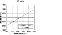
- FIG. 3 is a diagram showing a formula for calculating transverse wave sound speed. 3 is a graph showing the relationship between the transverse sound velocity of the electrode material and the center point CP of the electrode thickness in the results of Study Examples 1 to 3.
- 2 is a graph showing the relationship between the transverse wave sound velocity and the sound velocity (acoustic wave sound velocity) V of the electrode material in the results of Study Examples 1 to 3.
- 2 is a graph showing the relationship between the transverse sound velocity of the electrode material and the fractional bandwidth ⁇ f in the results of Study Examples 1 to 3.
- 12 is a table showing FEM simulation conditions regarding Al electrode thickness in study example 5.
- 12 is a graph showing FEM simulation results regarding the relationship between Al electrode thickness and fractional bandwidth ⁇ f in study example 5.
- 12 is a graph showing FEM simulation results regarding the relationship between Al electrode thickness and sound velocity V in study example 5.
- 12 is a table showing FEM simulation conditions regarding LN thickness in study example 5.
- 12 is a graph showing FEM simulation results regarding the relationship between LN thickness and fractional bandwidth ⁇ f in study example 5.
- 12 is a graph showing FEM simulation results regarding the relationship between LN thickness and sound velocity V in study example 5.
- 12 is a table showing FEM simulation conditions regarding LN cut angles in study example 5.
- 12 is a graph showing FEM simulation results regarding the relationship between the LN cut angle and the fractional bandwidth ⁇ f in Study Example 5.
- 12 is a graph showing FEM simulation results regarding the relationship between the LN cut angle and the sound velocity V in study example 5.
- 12 is a table showing FEM simulation conditions regarding LN propagation angle in study example 5.
- 12 is a graph showing FEM simulation results regarding the relationship between LN propagation angle and fractional bandwidth ⁇ f in study example 5.
- 12 is a graph showing FEM simulation results regarding the relationship between LN propagation angle and sound speed V in study example 5.
- 12 is a table showing FEM simulation conditions regarding Cu electrode thickness in Study Example 6.
- 12 is a graph showing FEM simulation results regarding the relationship between Cu electrode thickness and fractional bandwidth ⁇ f in Study Example 6.
- 12 is a graph showing FEM simulation results regarding the relationship between Cu electrode thickness and sound velocity V in study example 6.
- 12 is a table showing FEM simulation conditions regarding LN thickness in Study Example 6.
- 12 is a graph showing FEM simulation results regarding the relationship between LN thickness and fractional bandwidth ⁇ f in study example 6.
- 12 is a graph showing FEM simulation results regarding the relationship between LN thickness and sound velocity V in study example 6.
- 12 is a table showing FEM simulation conditions regarding LN cut angles in study example 6.
- 12 is a graph showing FEM simulation results regarding the relationship between the LN cut angle and the fractional bandwidth ⁇ f in study example 6.
- 12 is a graph showing FEM simulation results regarding the relationship between the LN cut angle and the sound velocity V in study example 6.
- 12 is a table showing FEM simulation conditions regarding LN propagation angle in study example 6.
- 12 is a graph showing FEM simulation results regarding the relationship between LN propagation angle and fractional bandwidth ⁇ f in study example 6.
- 12 is a graph showing FEM simulation results regarding the relationship between LN propagation angle and sound speed V in study example 6.
- 12 is a table showing FEM simulation conditions regarding Pt electrode thickness in Study Example 7.
- 12 is a graph showing FEM simulation results regarding the relationship between Pt electrode thickness and fractional bandwidth ⁇ f in Study Example 7.
- 12 is a graph showing FEM simulation results regarding the relationship between Pt electrode thickness and sound velocity V in study example 7.
- 12 is a table showing FEM simulation conditions regarding LN thickness in Study Example 7.
- 12 is a graph showing FEM simulation results regarding the relationship between LN thickness and fractional bandwidth ⁇ f in study example 7.
- 12 is a graph showing FEM simulation results regarding the relationship between LN thickness and sound velocity V in study example 7.
- 12 is a table showing FEM simulation conditions regarding LN cut angle in study example 7.
- 12 is a graph showing FEM simulation results regarding the relationship between the LN cut angle and the fractional bandwidth ⁇ f in study example 7.
- 12 is a graph showing FEM simulation results regarding the relationship between the LN cut angle and the sound velocity V in study example 7.
- 12 is a table showing FEM simulation conditions regarding LN propagation angle in study example 7.
- 12 is a graph showing FEM simulation results regarding the relationship between LN propagation angle and fractional bandwidth ⁇ f in study example 7.
- 12 is a graph showing FEM simulation results regarding the relationship between LN propagation angle and sound speed V in study example 7.
- 7 is a graph showing the relationship between the transverse sound velocity of the electrode material and the center point CP of the electrode thickness in the results of Study Examples 5 to 7.
- 7 is a graph showing the relationship between the transverse wave sound velocity and the sound velocity (elastic wave sound velocity) V of the electrode material in the results of Study Examples 5 to 7.
- 7 is a graph showing the relationship between the transverse sound velocity of the electrode material and the fractional bandwidth ⁇ f in the results of Study Examples 5 to 7.
- FIG. 3 is a perspective view showing another structural example of the elastic wave device according to an embodiment of the present disclosure.
- FIG. 3 is a cross-sectional view showing another configuration example of an elastic wave device according to an embodiment of the present disclosure.
- FIG. 3 is a cross-sectional view showing another configuration example of an elastic wave device according to an embodiment of the present disclosure.
- 1 is a diagram illustrating a schematic configuration of a communication device.
- the elastic wave device in this embodiment may optionally include known constituent members that are not shown in the respective figures referred to. Furthermore, the dimensions of the members in each figure do not faithfully represent the dimensions of the actual constituent members and the dimensional ratios of each member.
- FIG. 1 is a perspective view showing a configuration example of an elastic wave device 100 in this embodiment.
- FIG. 2 is a sectional view showing a configuration example of the elastic wave device 100 in this embodiment.
- the specific shape of the IDT electrode 3 included in the acoustic wave device 100 in this embodiment is not particularly limited, and the electrode fingers 32 of the IDT electrode 3 may be formed in various known shapes. Therefore, in FIG. 1, the electrode fingers 32 of the IDT electrode 3 are simply shown by diagonal hatching. Further, in FIG. 2 and the cross-sectional views referred to in the following description, for clarity of illustration, illustrations (cut-away cross-sectional views) are shown in which members on the back side of the cross-section are omitted.
- an elastic wave device 100 may include at least one resonator 1.
- the input terminal Tin and the output terminal Tout may be connected to the resonator 1.
- the resonator 1 may be configured as a frequency filter (SAW filter) that filters an electrical signal input to an input terminal Tin and outputs the filtered electrical signal to an output terminal Tout.
- SAW filter frequency filter
- the elastic wave device 100 may include a support substrate 5 , a piezoelectric layer 2 in direct or indirect contact with the support substrate 5 , and an IDT electrode 3 located on the piezoelectric layer 2 .
- the IDT electrode 3 is also called an excitation electrode.
- the elastic wave device 100 in this embodiment is configured to effectively excite an asymmetric zero-order moderam wave. This will be described in detail later.
- each of the plurality of resonators 1 may share the support substrate 5 and the piezoelectric layer 2.
- Each of the plurality of resonators 1 may have an individual IDT electrode 3.
- the support substrate 5 supports each part of the acoustic wave device 100.
- the specific material of the support substrate 5 is not particularly limited, and may be, for example, a Si substrate.
- the piezoelectric layer 2 may be made of a single crystal material having piezoelectricity.
- the material of the piezoelectric layer 2 may be lithium tantalate (also referred to as LiTaO 3 :LT) or lithium niobate (also referred to as LiNbO 3 :LN).
- the acoustic wave device 100 may include an intermediate layer 6 located between the support substrate 5 and the piezoelectric layer 2.
- the support substrate 5 and the piezoelectric layer 2 may be bonded to each other via an intermediate layer 6.
- the constituent material of the intermediate layer 6 may typically be silicon oxide (SiO x ).
- the intermediate layer 6 may be a SiO 2 film.
- the elastic wave device 100 does not need to have the intermediate layer 6.
- Acoustic wave device 100 with intermediate layer 6 may be easier to manufacture than acoustic wave device 100 without intermediate layer 6.
- the bonding layer formed between the support substrate 5 and the piezoelectric layer 2 by bonding them in the manufacturing process of the acoustic wave device 100 is The filter characteristics of device 100 may be adversely affected. This is because the distance between the bonding layer and the surface of the piezoelectric layer 2 on the side far from the support substrate 5 becomes relatively short.
- the IDT electrode 3 is typically an interdigitated electrode in which an electrode pair consisting of a first electrode finger 32a of a positive electrode and a second electrode finger 32b of a negative electrode is arranged periodically.
- the propagation direction of the SAW excited by the IDT electrode 3 is a direction perpendicular to the direction in which the first electrode finger 32a and the second electrode finger 32b extend.
- the propagation direction of the SAW propagating on the surface of the piezoelectric layer 2 is the x direction
- the thickness direction of each member of the acoustic wave device 100 is the z direction, which is orthogonal to the x direction and the z direction.
- the direction be the y direction.
- the positive direction in the z direction may be referred to as an upward direction
- the negative direction in the z direction may be referred to as a downward direction.
- the orthogonal coordinate system (xyz coordinate system) shown in FIG. 1 is appropriately shown in each drawing referred to in the following description.
- the IDT electrode 3 may have two bus bars 31 (a first bus bar 31a and a second bus bar 31b) facing each other in the y direction.
- the IDT electrode 3 may have a plurality of first electrode fingers 32a connected to the first bus bar 31a and a plurality of second electrode fingers 32b connected to the second bus bar 31b.
- the first electrode finger 32a may extend in the y direction from the first bus bar 31a toward the second bus bar 31b.
- the second electrode finger 32b may extend in the y direction from the second bus bar 31b toward the first bus bar 31a.
- the first electrode fingers 32a and the second electrode fingers 32b may be alternately and repeatedly positioned on the piezoelectric layer 2 at approximately constant intervals in the x direction.
- the first electrode finger 32a and the second electrode finger 32b may be collectively referred to as the electrode finger 32.
- the electrode finger pitch (pitch of electrode fingers) p in the IDT electrode 3 may be the distance between the centers of two adjacent electrode fingers 32 (in other words, the repetition interval of the electrode fingers 32) in the x direction.
- the length of one of the electrode fingers 32 (the first electrode finger 32a or the second electrode finger 32b) in the x direction is referred to as the width w.
- the first electrode finger 32a and the second electrode finger 32b may have the same or substantially the same width w.
- substantially the same means substantially the same, and means allowing for a difference (error) in dimensions of about ⁇ 5%. This also applies to the following description, and repeated explanation will be omitted.
- the width w may be set as appropriate, for example, depending on the electrical characteristics required of the elastic wave device 100.
- the width w may be set corresponding to the electrode finger pitch p.
- the ratio (w/p) of the width w to the electrode finger pitch p is referred to as duty.
- the width w and the electrode finger pitch p may be constant (that is, the duty is constant) over the entire electrode finger 32.
- constant is not limited to strictly no change, but is used in the sense of allowing an error of approximately ⁇ 5 degrees.
- the electrode finger 32 may have a thin flat plate shape extending in the y direction and made of a metal material, for example.
- the metal may be aluminum (Al), copper (Cu), or platinum (Pt).
- the structure (material and thickness) of the electrode finger 32 will be described in more detail later.
- the IDT electrode 3 may further include a protective layer covering the electrode fingers 32.
- the material of the protective layer may be, for example, SiO 2 , and any insulating material commonly used as a protective film may be used as appropriate.
- the elastic wave device 100 may include a pair of reflectors 4a and 4b corresponding to the IDT electrode 3.
- the reflectors 4a and 4b are also generically referred to as reflectors 4.
- the reflector 4 may be positioned to sandwich the IDT electrode 3 in the x direction.
- a relatively low frequency band for example, a frequency band of 700 MHz to 900 MHz (hereinafter, for convenience of explanation, may be referred to as a "target frequency band") is used for communication.
- the value calculated by dividing the bandwidth (pass band width) by the center frequency (resonant frequency) is called the fractional bandwidth (herein sometimes referred to as "fractional bandwidth ⁇ f").
- the fractional bandwidth ⁇ f the fractional bandwidth
- the minimum value is 1.1% in the downstream communication of Band 6. Therefore, the present inventors set the conditions required for the filter characteristics of the elastic wave device 100 to have a bandwidth in the target frequency band and have a fractional bandwidth ⁇ f of 1.1% or more.
- Lamb waves having a vibration plane perpendicular to the surface of the piezoelectric layer 2 are one type of various propagation modes in SAW, and are known to have multimodality.
- an asymmetric zero-order mode Lamb wave also referred to as an "A0 mode Lamb wave”
- “sonic velocity” is the propagation velocity of the elastic wave used in the elastic wave device 100, and can also be said to be the phase velocity.
- the present inventors came up with the idea of reducing the size of the elastic wave device 100 by lowering the sound velocity V using the A0 mode ram wave.
- the sound velocity V of the A0 mode ram wave decreases as the thickness of the piezoelectric layer 2 becomes thinner.
- the present inventors used finite element method (FEM) simulation to evaluate the relationship between the specific structure and filter characteristics of the elastic wave device 100 having the basic structure (bonded structure) described above. Then, the inventors discovered the conditions stipulated regarding the structure of the elastic wave device 100, and came up with the present invention.
- FEM finite element method
- FIG. 3 is a diagram showing an outline of an FEM simulation model of an elastic wave device.
- FIG. 4 is a table showing FEM simulation conditions.
- a piezoelectric layer 2 is bonded above a support substrate 5 via an intermediate layer 6, and a first It has an electrode finger 32a and a second electrode finger 32b.
- the material of the electrode fingers 32 was Al, Cu, or Pt.
- the material of the piezoelectric layer 2 was LT (LiTaO 3 ) or LN (LiNbO 3 ).
- the thickness of the electrode fingers 32, the thickness of the piezoelectric layer 2, the cut angle, and the propagation angle were used as variables. Further, in the FEM simulation, the electrode finger pitch p was fixed at 1.0 ⁇ m and the duty was fixed at 0.5.
- the wavelength ⁇ of the asymmetric zero-order mode ram wave is 2.0 ⁇ m, which is twice the electrode finger pitch p.
- the thickness of the intermediate layer 6 did not significantly affect the filter characteristics. Therefore, in the FEM simulation described below, the material of the intermediate layer 6 was SiO 2 and the thickness was fixed at 0.5 ⁇ as a general value.
- the Euler angles of the piezoelectric layer 2 can generally be expressed as ( ⁇ , ⁇ , ⁇ ). In the FEM simulation described below, ⁇ was fixed at 0°, and ⁇ and ⁇ were made variables. The meanings of ⁇ , ⁇ , and ⁇ in the Euler angle of the piezoelectric layer 2 can be understood based on common technical knowledge. For the sake of brevity, a detailed description of the Euler angle of the piezoelectric layer 2 will be omitted.
- the condition range required for each variable and the center point CP within that range were specified.
- the "center point CP" is not the median value of the range, but is a value selected in consideration of the balance of the characteristics of both the fractional bandwidth ⁇ f and the speed of sound V, and the reason for its selection is as follows. The individual FEM simulation results will be described later.
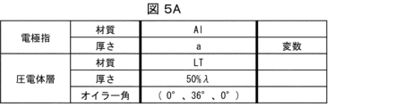
- FIG. 5A is a table showing FEM simulation conditions regarding the Al electrode thickness in Examination Example 1.
- FIG. 5B is a graph showing the FEM simulation results regarding the relationship between the Al electrode thickness and the fractional bandwidth ⁇ f in Examination Example 1.
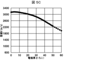
- FIG. 5C is a graph showing the FEM simulation results regarding the relationship between the Al electrode thickness and the sound velocity V in Study Example 1.
- the Euler angles of the piezoelectric layer 2 were fixed to common values (0°, 36°, 0°). Further, the LT thickness was fixed at 50% ⁇ .
- the fractional bandwidth ⁇ f is 1.1% fr or more when the Al electrode thickness is within the range of 0.6% ⁇ to 50.0% ⁇ .
- the maximum point in the fitting curve of the plot of the fractional bandwidth ⁇ f shown in FIG. 5B was selected as the center point CP. That is, the center point CP of the Al electrode thickness in Examination Example 1 was set to 30% ⁇ .
- the unit of the fractional bandwidth ⁇ f may be expressed as "%fr". This means that it is expressed as a percentage of the value calculated by dividing the passband width by the resonance frequency (fr).
- FIG. 6A is a table showing FEM simulation conditions regarding LT thickness in Study Example 1.
- FIG. 6B is a graph showing the FEM simulation results regarding the relationship between the LT thickness and the fractional bandwidth ⁇ f in Study Example 1.
- FIG. 6C is a graph showing the FEM simulation results regarding the relationship between the LT thickness and the sound velocity V in Study Example 1.
- the Euler angle of the piezoelectric layer 2 was fixed at the general values (0°, 36°, 0°)
- the Al electrode thickness was set using the above-mentioned FEM simulation. It was fixed at 30% ⁇ , which is the center point CP in the simulation results.
- the fractional bandwidth ⁇ f is 1.1%fr or more.
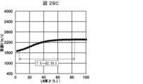
- the sound velocity V increases as the LT thickness increases, and the value of the sound velocity V becomes saturated when the LT thickness is 87.5% ⁇ .
- a point where the fractional bandwidth ⁇ f is relatively large and the speed of sound B is relatively slow was selected as the center point CP. That is, the center point CP of the LT thickness in Study Example 1 was set to 32.5% ⁇ .
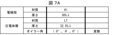
- FIG. 7A is a table showing FEM simulation conditions regarding the LT cut angle in Study Example 1.
- FIG. 7B is a graph showing the FEM simulation results regarding the relationship between the LT cut angle and the fractional bandwidth ⁇ f in Study Example 1.
- FIG. 7C is a graph showing the FEM simulation results regarding the relationship between the LT cut angle and the sound speed V in Study Example 1.
- the Al electrode thickness was fixed at 30% ⁇ , which is the center point CP in the above FEM simulation results, and the LT thickness was fixed at the center point CP in the above FEM simulation results. It was fixed at a certain 32.5% ⁇ .
- the fractional bandwidth ⁇ f is 1.1% fr or more when the LT cut angle is in the range of 8° or more and 74° or less.
- the center point CP of the LT cut angle was set to 36°.
- FIG. 7B it can be seen that the center point CP of the LT cut angle is located near the maximum point in the fitting curve of the plot of the fractional bandwidth ⁇ f.
- FIG. 8A is a table showing FEM simulation conditions regarding the LT propagation angle in study example 1.
- FIG. 8B is a graph showing the FEM simulation results regarding the relationship between the LT propagation angle and the fractional bandwidth ⁇ f in Study Example 1.
- FIG. 8C is a graph showing the FEM simulation results regarding the relationship between the LT propagation angle and the sound speed V in Study Example 1.
- the Al electrode thickness was fixed at 30% ⁇ , which is the center point CP in the above-mentioned FEM simulation results.
- the LT thickness was fixed at 32.5% ⁇ , which is the center point CP in the above-mentioned FEM simulation results, and the LT cut angle was fixed at 36°.
- the fractional bandwidth is It can be seen that ⁇ f is 1.1%fr or more.
- the fitting curve of the plot of the fractional bandwidth ⁇ f shown in FIG. 8B actually has an upwardly convex peak because the LT propagation angles of 0° and 180° are equivalent.
- the maximum point of the fitting curve was selected as the center point CP. That is, the center point CP of the LT propagation angle was set to 0°.
- the main component of the constituent material of the piezoelectric layer 2 is lithium tantalate (LT), and the thickness is 20 mm. .0% ⁇ or more and 87.5% ⁇ or less. Furthermore, assuming the Euler angles of the piezoelectric layer 2 as ( ⁇ , ⁇ , ⁇ ), ⁇ is ⁇ 5° or more and 5° or less, ⁇ is 8° or more and 74° or less, and ⁇ is ⁇ 26° or more and 26° or less.
- the main component of the constituent material of the IDT electrode 3 is Al, and the thickness is 0.6% ⁇ or more and 50.0% ⁇ or less.
- the above ⁇ is the wavelength ⁇ of the A0 mode ram wave, and is defined as twice the length of the pitch p of the plurality of electrode fingers 32 included in the IDT electrode 3.
- the above definition of ⁇ is the same in the following description of this specification, and repeated description will be omitted.
- the Euler angle ⁇ of the piezoelectric layer 2 is defined in the range of ⁇ 5° or more and 5° or less from the viewpoint of allowing errors in the manufacturing process.
- the characteristics of the elastic wave device 100 hardly change in the range where ⁇ is ⁇ 5° or more and 5° or less.
- the resonator 1 can effectively excite or receive the A0 moderam wave.
- the elastic wave device 100 in configuration example 1 functions as a SAW filter that utilizes the A0 mode ram wave, and has frequency characteristics in which the fractional bandwidth ⁇ f is 1.1% fr or more.
- the sound velocity V of the conventional SAW is about 4000 m/s
- the sound velocity V of the A0 moderam wave is slower than that of the conventional SAW.
- the elastic wave device 100 having a certain resonant frequency with an elastic wave device (conventional elastic wave device) that uses a conventional SAW and has the same resonant frequency
- the resonator 1 can be downsized by using the A0 mode ram wave that propagates at a speed of sound V that is slower than that of the conventional SAW.
- the elastic wave device 100 can be effectively miniaturized while having frequency characteristics with a fractional bandwidth ⁇ f of 1.1% fr or more.
- the main component of the constituent material is component A
- the proportion of the component A to the entire constituent material is greater than 50% by mass. This also applies to the following description in this specification, and repeated description will be omitted.
- the piezoelectric layer 2 may be made of LT, or may be made substantially of LT.
- the IDT electrode 3 may be made of Al, or may be made substantially of Al.
- substantially consisting of component B means that the proportion of component B to the entire constituent material is 90% by mass or more. This also applies to the following description in this specification, and repeated description will be omitted.
- the piezoelectric layer 2 may contain LT in an amount of 70% by mass or more, or may contain LT in an amount of 80% by mass or more.
- the remainder of the constituent material of the piezoelectric layer 2 other than LT may consist of arbitrary additive components and unavoidable impurities.
- the IDT electrode 3 may contain Al at 70% by mass or more, or may contain Al at 80% by mass or more.
- the remainder of the constituent material of the IDT electrode 3 other than Al may consist of arbitrary additive components and unavoidable impurities.
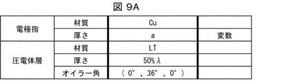
- FIG. 9A is a table showing FEM simulation conditions regarding the Cu electrode thickness in Examination Example 2.
- FIG. 9B is a graph showing the FEM simulation results regarding the relationship between the Cu electrode thickness and the fractional bandwidth ⁇ f in Examination Example 2.
- FIG. 9C is a graph showing the FEM simulation results regarding the relationship between the Cu electrode thickness and the sound velocity V in Examination Example 2.
- the Euler angles of the piezoelectric layer 2 were fixed to common values (0°, 36°, 0°).
- the fractional bandwidth ⁇ f is 1.1% fr or more when the Cu electrode thickness is in the range of 0.2% ⁇ to 50.0% ⁇ .
- the maximum point in the fitting curve of the plot of the fractional bandwidth ⁇ f shown in FIG. 9B was selected as the center point CP. That is, the center point CP of the Cu electrode thickness in Examination Example 2 was set to 20% ⁇ .
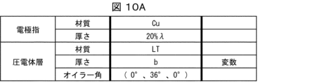
- FIG. 10A is a table showing FEM simulation conditions regarding LT thickness in Study Example 2.
- FIG. 10B is a graph showing the FEM simulation results regarding the relationship between the LT thickness and the fractional bandwidth ⁇ f in Study Example 2.
- FIG. 10C is a graph showing the FEM simulation results regarding the relationship between the LT thickness and the sound velocity V in Study Example 2.
- the Euler angle of the piezoelectric layer 2 was fixed at the common values (0°, 36°, 0°), and the Cu electrode thickness was It was fixed at 20% ⁇ , which is the center point CP in the simulation results.
- the fractional bandwidth ⁇ f is 1.1%fr or more.
- the sound velocity V increases as the LT thickness increases, and the value of the sound velocity V becomes saturated when the LT thickness is 90.0% ⁇ .
- a point where the fractional bandwidth ⁇ f is relatively large and the speed of sound B is relatively slow was selected as the center point CP. That is, the center point CP of the LT thickness in Examination Example 2 was set to 37.5% ⁇ .
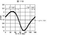
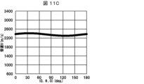
- FIG. 11A is a table showing FEM simulation conditions regarding the LT cut angle in study example 2.
- FIG. 11B is a graph showing the FEM simulation results regarding the relationship between the LT cut angle and the fractional bandwidth ⁇ f in study example 2.
- FIG. 11C is a graph showing the FEM simulation results regarding the relationship between the LT cut angle and the sound velocity V in study example 2.
- the Cu electrode thickness was fixed at 20% ⁇ , which is the center point CP in the above FEM simulation results, and the LT thickness was fixed at the center point CP in the above FEM simulation results. It was fixed at a certain 37.5% ⁇ .
- the fractional bandwidth is It can be seen that ⁇ f is 1.1%fr or more.
- the center point CP of the LT cut angle was set to 36°.
- FIG. 11B it can be seen that the center point CP of the LT cut angle is located near the maximum point in the fitting curve of the plot of the fractional bandwidth ⁇ f.
- FIG. 12A is a table showing FEM simulation conditions regarding the LT propagation angle in study example 2.
- FIG. 12B is a graph showing the FEM simulation results regarding the relationship between the LT propagation angle and the fractional bandwidth ⁇ f in study example 2.
- FIG. 12C is a graph showing the FEM simulation results regarding the relationship between the LT propagation angle and the sound speed V in study example 2.
- the Cu electrode thickness was fixed at 20% ⁇ , which is the center point CP in the above-mentioned FEM simulation results.
- the LT thickness was fixed at 37.5% ⁇ , which is the center point CP in the above-mentioned FEM simulation results, and the LT cut angle was fixed at 36°.
- the fractional bandwidth is It can be seen that ⁇ f is 1.1%fr or more.
- the fitting curve of the plot of the fractional bandwidth ⁇ f shown in FIG. 12B actually has an upwardly convex peak because the LT propagation angles of 0° and 180° are equivalent.
- the maximum point of the fitting curve was selected as the center point CP. That is, the center point CP of the LT propagation angle was set to 0°.
- the main component of the constituent material of the piezoelectric layer 2 is lithium tantalate (LT), and the thickness is 17 mm. .5% ⁇ or more and 90.0% ⁇ or less. Further, assuming the Euler angles of the piezoelectric layer 2 as ( ⁇ , ⁇ , ⁇ ), ⁇ is -5° or more and 5° or less, ⁇ is -20° or more and 80° or less, and ⁇ is -40° or more and 40° or less. .
- the main component of the constituent material of the IDT electrode 3 is Cu, and the thickness is 0.2% ⁇ or more and 58.0% ⁇ or less.
- the Euler angle ⁇ of the piezoelectric layer 2 is defined in the range of ⁇ 5° or more and 5° or less from the viewpoint of allowing errors in the manufacturing process.
- the piezoelectric layer 2 may be the same as in the first configuration example.
- the IDT electrode 3 may be made of Cu or may be made substantially of Cu.
- the IDT electrode 3 may contain 70% by mass or more of Cu, or may contain 80% by mass or more of Cu.
- the remainder of the constituent material of the IDT electrode 3 other than Cu may consist of arbitrary additive components and unavoidable impurities.
- the resonator 1 can effectively excite or receive the A0 mode ram wave.
- the resonator 1 can be downsized by using the A0 mode ram wave that propagates at a speed of sound V that is slower than that of the conventional SAW.
- the elastic wave device 100 can be effectively miniaturized while having frequency characteristics with a fractional bandwidth ⁇ f of 1.1% fr or more. This is the same in the following configuration examples 3 to 8, although a repeated explanation will be omitted.
- FIG. 13A is a table showing FEM simulation conditions regarding the Pt electrode thickness in Study Example 3.
- FIG. 13B is a graph showing the FEM simulation results regarding the relationship between the Pt electrode thickness and the fractional bandwidth ⁇ f in Study Example 3.
- FIG. 13C is a graph showing the FEM simulation results regarding the relationship between the Pt electrode thickness and the sound velocity V in Study Example 3.
- the Euler angles of the piezoelectric layer 2 were fixed to common values (0°, 36°, 0°).
- the fractional bandwidth ⁇ f is 1.1% fr or more when the Pt electrode thickness is within the range of 0.3% ⁇ to 74.0% ⁇ .
- the maximum point in the fitting curve of the plot of the fractional bandwidth ⁇ f shown in FIG. 13B was selected as the center point CP. That is, the center point CP of the Pt electrode thickness in Study Example 3 was set to 13% ⁇ .
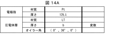
- FIG. 14A is a table showing FEM simulation conditions regarding LT thickness in Study Example 3.
- FIG. 14B is a graph showing the FEM simulation results regarding the relationship between the LT thickness and the fractional bandwidth ⁇ f in Study Example 3.
- FIG. 14C is a graph showing the FEM simulation results regarding the relationship between the LT thickness and the sound velocity V in Study Example 3.
- the Euler angle of the piezoelectric layer 2 was fixed at the general values (0°, 36°, 0°), and the Pt electrode thickness was It was fixed at 13% ⁇ , which is the center point CP in the simulation results.
- the fractional bandwidth ⁇ f is 1.1%fr or more.
- the sound velocity V increases as the LT thickness increases, and the value of the sound velocity V becomes saturated when the LT thickness is 85.0% ⁇ .
- a point where the fractional bandwidth ⁇ f is relatively large and the speed of sound B is relatively slow was selected as the center point CP. That is, the center point CP of the LT thickness in Study Example 3 was set to 40.0% ⁇ .
- FIG. 15A is a table showing FEM simulation conditions regarding the LT cut angle in study example 3.
- FIG. 15B is a graph showing the FEM simulation results regarding the relationship between the LT cut angle and the fractional bandwidth ⁇ f in Study Example 3.
- FIG. 15C is a graph showing the FEM simulation results regarding the relationship between the LT cut angle and the sound velocity V in Study Example 3.
- the Pt electrode thickness was fixed at 13% ⁇ , which is the center point CP in the above-mentioned FEM simulation results.
- the LT thickness was fixed at 40.0% ⁇ , which is the center point CP in the above-mentioned FEM simulation results.
- the fractional bandwidth is It can be seen that ⁇ f is 1.1%fr or more.
- the center point CP of the LT cut angle was set to 36°.
- FIG. 15B it can be seen that the center point CP of the LT cut angle is located near the maximum point in the fitting curve of the plot of the fractional bandwidth ⁇ f.
- FIG. 16A is a table showing FEM simulation conditions regarding the LT propagation angle in study example 3.
- FIG. 16B is a graph showing the FEM simulation results regarding the relationship between the LT propagation angle and the fractional bandwidth ⁇ f in Study Example 3.
- FIG. 16C is a graph showing the FEM simulation results regarding the relationship between the LT propagation angle and the sound speed V in Study Example 3.
- the Pt electrode thickness was fixed at 13% ⁇ , which is the center point CP in the above-mentioned FEM simulation results.
- the LT thickness was fixed at 40.0% ⁇ , which is the center point CP in the above-mentioned FEM simulation results, and the LT cut angle was fixed at 36°.
- the fractional bandwidth is It can be seen that ⁇ f is 1.1%fr or more.
- the fitting curve of the plot of the fractional bandwidth ⁇ f shown in FIG. 16B actually has an upwardly convex peak because the LT propagation angles of 0° and 180° are equivalent.
- the maximum point of the fitting curve was selected as the center point CP. That is, the center point CP of the LT propagation angle was set to 0°.
- the main component of the constituent material of the piezoelectric layer 2 is lithium tantalate (LT), and the thickness is 1.5 mm. .0% ⁇ or more and 85.0% ⁇ or less. Further, assuming the Euler angles of the piezoelectric layer 2 as ( ⁇ , ⁇ , ⁇ ), ⁇ is -5° or more and 5° or less, ⁇ is -40° or more and 86° or less, and ⁇ is -50° or more and 50° or less. .
- the main component of the constituent material of the IDT electrode 3 is Pt, and the thickness is 0.3% ⁇ or more and 74.0% ⁇ or less.
- the Euler angle ⁇ of the piezoelectric layer 2 is defined in the range of ⁇ 5° or more and 5° or less from the viewpoint of allowing errors in the manufacturing process.
- the piezoelectric layer 2 may be the same as in the configuration example 1 above.
- the IDT electrode 3 may be made of Pt or may be made substantially of Pt.
- the IDT electrode 3 may contain 70% by mass or more of Pt, or may contain 80% by mass or more of Pt.
- the remainder of the constituent material of the IDT electrode 3 other than Pt may consist of arbitrary additive components and unavoidable impurities.
- FIG. 17A is a table showing transverse sound speeds of major metal materials.
- FIG. 17B is a diagram showing a formula for calculating transverse wave sound speed.
- V is the transverse sound velocity (m/s)
- E is Young's modulus (Pa)
- ⁇ is the density (kg/m 3 )
- ⁇ is Poisson's ratio.
- the transverse sound velocities of Al, Cu, and Pt used in Study Examples 1 to 3 above are 2571 m/s, 1804 m/s, and 1244 m/s, respectively.
- the center point CP of the Al electrode thickness is 30% ⁇
- the sound velocity (acoustic wave sound speed) V at the center point CP is about 3000 m/s
- the fractional bandwidth at the center point CP is ⁇ f was approximately 1.6 (see Figures 5A-5C).
- the center point CP of the Cu electrode thickness is 20% ⁇
- the sound velocity (acoustic wave sound speed) V at the center point CP is about 2500 m/s
- the ratio at the center point CP is The bandwidth ⁇ f was approximately 2.1 (see FIGS. 9A-9C).
- the center point CP of the Pt electrode thickness is 13% ⁇
- the sound velocity (acoustic wave sound velocity) V at the center point CP is about 2300 m/s
- the fractional bandwidth at the center point CP is ⁇ f was approximately 2.5 (see FIGS. 13A-13C).
- FIG. 18A is a graph showing the relationship between the transverse sound velocity of the electrode material and the center point CP of the electrode thickness in the results of Study Examples 1 to 3.
- FIG. 18B is a graph showing the relationship between the transverse wave sonic velocity and the sonic velocity (acoustic wave sonic velocity) V of the electrode material in the results of Study Examples 1 to 3.
- FIG. 18C is a graph showing the relationship between the transverse sound velocity of the electrode material and the fractional bandwidth ⁇ f in the results of Study Examples 1 to 3.
- 18A to 18C show straight lines and determination coefficients calculated by approximating the plots corresponding to the results of Study Examples 1 to 3 using linear functions. As shown in FIGS. 18A to 18C, it can be seen that the transverse wave sonic velocity of the electrode material, the sonic velocity (acoustic wave sonic velocity) V, and the fractional bandwidth ⁇ f have a linear function relationship with each other.
- the fractional bandwidth ⁇ f is 1.1% fr or more.
- energy tends to concentrate around the electrode, and as a result, the fractional bandwidth ⁇ f tends to increase.
- Au had the lowest transverse wave sound velocity, which was 658 m/s. Based on this, the lower limit of the transverse sound velocity of the electrode material was set to 500 m/s.
- the main component of the constituent material of the piezoelectric layer 2 is lithium tantalate, and the thickness is The length is 15.0% ⁇ or more and 90.0% ⁇ or less. Further, assuming the Euler angles of the piezoelectric layer 2 as ( ⁇ , ⁇ , ⁇ ), ⁇ is -5° or more and 5° or less, ⁇ is -40° or more and 86° or less, and ⁇ is -50° or more and 50° or less. .
- the main component of the constituent material of the IDT electrode 3 is a metal having a transverse sound velocity of 500 m/s or more and 3473 m/s or less, and the thickness is 0.2% ⁇ or more and 74.0% ⁇ or less.
- the main component of the constituent material of the piezoelectric layer 2 is tantalum acid. It is lithium and has a thickness of 20.0% ⁇ or more and 85.0% ⁇ or less. Furthermore, assuming the Euler angles of the piezoelectric layer 2 as ( ⁇ , ⁇ , ⁇ ), ⁇ is ⁇ 5° or more and 5° or less, ⁇ is 8° or more and 74° or less, and ⁇ is ⁇ 26° or more and 26° or less.
- the main component of the constituent material of the IDT electrode 3 is a metal having a transverse sound velocity of 500 m/s or more and 3473 m/s or less, and the thickness is 0.6% ⁇ or more and 50.0% ⁇ or less.
- the piezoelectric layer 2 may be the same as in the first configuration example.
- the IDT electrode 3 may be made of a metal having a transverse sound velocity of 500 m/s or more and 3473 m/s or less (hereinafter referred to as "specific metal M1"), or may be substantially made of the specific metal M1.
- the main component of the constituent material may be the specific metal M1.
- the main component of the constituent material of the IDT electrode 3 may be specified depending on the electrode structure of the IDT electrode 3.
- the thickest layer among the plurality of layers constituting the laminated structure can have the material with the highest concentration as the main component.
- the average value of the transverse sound velocity of each material of the plurality of layers constituting the laminated structure may be regarded as the transverse sound velocity of the constituent material of the IDT electrode 3.
- the average value is, for example, 500 m/s or more and 3473 m/s. / May be within the following range. If the electrode has a laminated structure, the sound velocity can also be calculated, for example, based on a volume average.
- the electrode in the IDT electrode 3 may be made of an alloy.
- the material with the highest concentration in the alloy composition may be the main component.
- the concentration in the alloy composition can be measured using, for example, EDX (Energy Dispersive X-ray Spectroscopy) or WDX (Wavelength-Dispersive X-ray Spectroscopy).
- the transverse sound velocity of the constituent material of the IDT electrode 3 calculated based on the density, Young's modulus, and Poisson's ratio of the alloy may be within a range of, for example, 500 m/s or more and 3473 m/s or less. Poisson's ratio is, for example, 0.3 in various alloys.
- FIG. 19A is a table showing FEM simulation conditions regarding Al electrode thickness in Study Example 5.
- FIG. 19B is a graph showing the FEM simulation results regarding the relationship between the Al electrode thickness and the fractional bandwidth ⁇ f in Study Example 5.
- FIG. 19C is a graph showing the FEM simulation results regarding the relationship between the Al electrode thickness and the sound velocity V in Study Example 5.
- the Euler angles of the piezoelectric layer 2 were fixed to common values (0°, 36°, 0°).
- the fractional bandwidth ⁇ f is 1.1% fr or more within the range where the Al electrode thickness is 100% ⁇ or less.
- An Al electrode thickness exceeding 100% ⁇ is not realistic, and an Al electrode thickness that is too thin is also not realistic. Therefore, the range of the Al electrode thickness can be defined as 0.05% ⁇ or more and 100.0% ⁇ or less.
- the range of the Al electrode thickness is defined as 0.05% ⁇ or more and 50.0% ⁇ or less You may.
- the part of the maximum point in the fitting curve of the plot of the fractional bandwidth ⁇ f shown in FIG. 19B was selected as the center point CP. That is, the center point CP of the Al electrode thickness in Study Example 5 was set to 24% ⁇ .
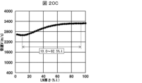
- FIG. 20A is a table showing FEM simulation conditions regarding LN thickness in Study Example 5.
- FIG. 20B is a graph showing FEM simulation results regarding the relationship between LN thickness and fractional bandwidth ⁇ f in Study Example 5.
- FIG. 20C is a graph showing the FEM simulation results regarding the relationship between LN thickness and sound velocity V in Study Example 5.
- the Euler angle of the piezoelectric layer 2 was fixed to the common values (0°, 36°, 0°)
- the Al electrode thickness was It was fixed at 24% ⁇ , which is the center point CP in the simulation results.
- the fractional bandwidth ⁇ f is 1.1%fr or more.
- the sound velocity V increases as the LN thickness increases, and the value of the sound velocity V becomes saturated when the LN thickness is 92.5% ⁇ .
- a point where the fractional bandwidth ⁇ f is relatively large and the speed of sound B is relatively slow was selected as the center point CP. That is, the center point CP of the LN thickness in Study Example 5 was set to 35.0% ⁇ .
- FIG. 21A is a table showing FEM simulation conditions regarding the LN cut angle in study example 5.
- FIG. 21B is a graph showing the FEM simulation results regarding the relationship between the LN cut angle and the fractional bandwidth ⁇ f in Study Example 5.
- FIG. 21C is a graph showing the FEM simulation results regarding the relationship between the LN cut angle and the sound speed V in Study Example 5.
- the Al electrode thickness was fixed at 24% ⁇ , which is the center point CP in the above FEM simulation results, and the LN thickness was fixed at the center point CP in the above FEM simulation results. It was fixed at a certain 35.0% ⁇ .
- the center point CP of the LN cut angle was set to 36°.
- FIG. 21B it can be seen that the center point CP of the LN cut angle is located near the maximum point in the fitting curve of the plot of the fractional bandwidth ⁇ f.
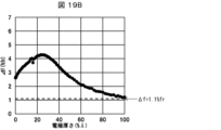
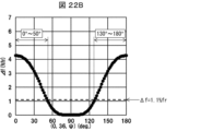
- FIG. 22A is a table showing FEM simulation conditions regarding the LN propagation angle in study example 5.
- FIG. 22B is a graph showing the FEM simulation results regarding the relationship between the LN propagation angle and the fractional bandwidth ⁇ f in Study Example 5.
- FIG. 22C is a graph showing the FEM simulation results regarding the relationship between the LN propagation angle and the sound speed V in Study Example 5.
- the Al electrode thickness was fixed at 24% ⁇ , which is the center point CP in the above-mentioned FEM simulation results.
- the LN thickness was fixed at 35.0% ⁇ , which is the center point CP in the above-mentioned FEM simulation results, and the LN cut angle was fixed at 36°.
- the fractional bandwidth is It can be seen that ⁇ f is 1.1%fr or more.
- the fitting curve of the plot of the fractional bandwidth ⁇ f shown in FIG. 22B actually has an upwardly convex peak because the LN propagation angles of 0° and 180° are equivalent.
- the maximum point of the fitting curve was selected as the center point CP. That is, the center point CP of the LN propagation angle was set to 0°.
- the main component of the constituent material of the piezoelectric layer 2 is lithium niobate, and the thickness is 10.0%. ⁇ or more and 92.5% ⁇ or less. Further, assuming the Euler angles of the piezoelectric layer 2 as ( ⁇ , ⁇ , ⁇ ), ⁇ is -5° or more and 5° or less, ⁇ is -38° or more and 90° or less, and ⁇ is -50° or more and 50° or less. .
- the main component of the constituent material of the IDT electrode 3 is Al, and the thickness is 0.05% ⁇ or more and 100.0% ⁇ or less.
- the piezoelectric layer 2 may be made of LN, or may be made substantially of LN.
- the piezoelectric layer 2 may contain 70% by mass or more of LN, or may contain 80% by mass or more of LN.
- the remainder of the constituent material of the piezoelectric layer 2 other than LN may consist of arbitrary additive components and unavoidable impurities.
- the IDT electrode 3 may be made of Al, or may be made substantially of Al.
- the IDT electrode 3 may contain 70% by mass or more of Al, or may contain 80% by mass or more of Al.
- the remainder of the constituent material of the IDT electrode 3 other than Al may consist of arbitrary additive components and unavoidable impurities.
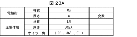
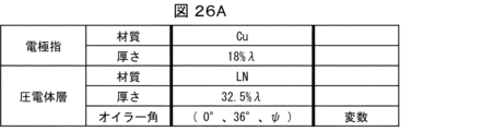
- FIG. 23A is a table showing FEM simulation conditions regarding Cu electrode thickness in Study Example 6.
- FIG. 23B is a graph showing the FEM simulation results regarding the relationship between the Cu electrode thickness and the fractional bandwidth ⁇ f in Study Example 6.
- FIG. 23C is a graph showing the FEM simulation results regarding the relationship between the Cu electrode thickness and the sound velocity V in Study Example 6.
- the Euler angles of the piezoelectric layer 2 were fixed to common values (0°, 36°, 0°).
- the range of the Cu electrode thickness can be defined as 0.05% ⁇ or more and 100.0% ⁇ or less.
- the range of the Cu electrode thickness is defined as 0.05% ⁇ or more and 66.0% ⁇ or less. You may.
- the part of the maximum point in the fitting curve of the plot of the fractional bandwidth ⁇ f shown in FIG. 23B was selected as the center point CP. That is, the center point CP of the Cu electrode thickness in Study Example 6 was set to 18% ⁇ .
- FIG. 24A is a table showing FEM simulation conditions regarding LN thickness in Study Example 6.
- FIG. 24B is a graph showing the FEM simulation results regarding the relationship between LN thickness and fractional bandwidth ⁇ f in Study Example 6.
- FIG. 24C is a graph showing the FEM simulation results regarding the relationship between LN thickness and sound velocity V in Study Example 6.
- the Euler angle of the piezoelectric layer 2 was fixed at the common values (0°, 36°, 0°), and the Cu electrode thickness was set using the above-mentioned FEM simulation. It was fixed at 18% ⁇ , which is the center point CP in the simulation results.
- the fractional bandwidth ⁇ f is 1.1%fr or more.
- the sound velocity V increases as the LN thickness increases, and the value of the sound velocity V becomes saturated when the LN thickness is 85.0% ⁇ .
- a point where the fractional bandwidth ⁇ f is relatively large and the speed of sound B is relatively slow was selected as the center point CP. That is, the center point CP of the LN thickness in Study Example 6 was set to 32.5% ⁇ .
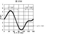
- FIG. 25A is a table showing FEM simulation conditions regarding the LN cut angle in study example 6.
- FIG. 25B is a graph showing the FEM simulation results regarding the relationship between the LN cut angle and the fractional bandwidth ⁇ f in Study Example 6.
- FIG. 25C is a graph showing the FEM simulation results regarding the relationship between the LN cut angle and the sound speed V in Study Example 6.
- the Cu electrode thickness was fixed at 18% ⁇ , which is the center point CP in the above FEM simulation results, and the LN thickness was fixed at the center point CP in the above FEM simulation results. It was fixed at a certain 32.5% ⁇ .
- the center point CP of the LN cut angle was set to 36°.
- FIG. 25B it can be seen that the center point CP of the LN cut angle is located near the maximum point in the fitting curve of the plot of the fractional bandwidth ⁇ f.
- FIG. 26A is a table showing FEM simulation conditions regarding the LN propagation angle in study example 6.
- FIG. 26B is a graph showing the FEM simulation results regarding the relationship between the LN propagation angle and the fractional bandwidth ⁇ f in Study Example 6.
- FIG. 26C is a graph showing the FEM simulation results regarding the relationship between the LN propagation angle and the sound speed V in Study Example 6.
- the Cu electrode thickness was fixed at 18% ⁇ , which is the center point CP in the above-mentioned FEM simulation results.
- the LN thickness was fixed at 32.5% ⁇ , which is the center point CP in the above-mentioned FEM simulation results, and the LN cut angle was fixed at 36°.
- the fractional bandwidth is It can be seen that ⁇ f is 1.1%fr or more.
- the fitting curve of the plot of the fractional bandwidth ⁇ f shown in FIG. 26B actually has an upwardly convex peak because the LN propagation angles of 0° and 180° are equivalent.
- the maximum point of the fitting curve was selected as the center point CP. That is, the center point CP of the LN propagation angle was set to 0°.
- the main component of the constituent material of the piezoelectric layer 2 is lithium niobate, and the thickness is 7.5% ⁇ or more 85. It is 0% ⁇ or less. Further, assuming the Euler angles of the piezoelectric layer 2 as ( ⁇ , ⁇ , ⁇ ), ⁇ is -5° or more and 5° or less, ⁇ is -52° or more and 84° or less, and ⁇ is -58° or more and 58° or less. .
- the main component of the constituent material of the IDT electrode 3 is Cu, and the thickness is 0.05% ⁇ or more and 100.0% ⁇ or less.
- the piezoelectric layer 2 may be the same as in configuration example 5 above.
- the IDT electrode 3 may be made of Cu or may be made substantially of Cu.
- the IDT electrode 3 may contain 70% by mass or more of Cu, or may contain 80% by mass or more of Cu.
- the remainder of the constituent material of the IDT electrode 3 other than Cu may consist of arbitrary additive components and unavoidable impurities.
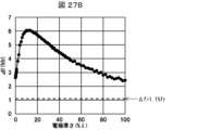
- FIG. 27A is a table showing FEM simulation conditions regarding Pt electrode thickness in Study Example 7.
- FIG. 27B is a graph showing the FEM simulation results regarding the relationship between the Pt electrode thickness and the fractional bandwidth ⁇ f in Study Example 7.
- FIG. 27C is a graph showing the FEM simulation results regarding the relationship between the Pt electrode thickness and the sound velocity V in Study Example 7.
- the Euler angles of the piezoelectric layer 2 were fixed to common values (0°, 36°, 0°).
- the fractional bandwidth ⁇ f is 1.1% fr or more within the range where the Pt electrode thickness is 100% ⁇ or less.
- a Pt electrode thickness exceeding 100% ⁇ is not realistic, and a Pt electrode thickness that is too thin is also not realistic. Therefore, the range of the Pt electrode thickness can be defined as 0.05% ⁇ or more and 100.0% ⁇ or less.
- the range of Pt electrode thickness is defined as 0.05% ⁇ or more and 86.0% ⁇ or less as the range in which the value of fractional bandwidth ⁇ f is equal to or greater than the value when the Pt electrode thickness is 0.05% ⁇ . You may.
- the part of the maximum point in the fitting curve of the plot of the fractional bandwidth ⁇ f shown in FIG. 27B was selected as the center point CP. That is, the center point CP of the Pt electrode thickness in Study Example 7 was set to 12% ⁇ .
- FIG. 28A is a table showing FEM simulation conditions regarding LN thickness in Study Example 7.
- FIG. 28B is a graph showing the FEM simulation results regarding the relationship between the LN thickness and the fractional bandwidth ⁇ f in Study Example 7.
- FIG. 28C is a graph showing the FEM simulation results regarding the relationship between LN thickness and sound velocity V in Study Example 7.
- the Euler angle of the piezoelectric layer 2 was fixed at the common values (0°, 36°, 0°)
- the Pt electrode thickness was It was fixed at 12% ⁇ , which is the center point CP in the simulation results.
- the fractional bandwidth ⁇ f is 1.1%fr or more.
- the sound velocity V increases as the LN thickness increases, and the value of the sound velocity V becomes saturated when the LN thickness is 82.5% ⁇ .
- a point where the fractional bandwidth ⁇ f is relatively large and the speed of sound B is relatively slow was selected as the center point CP. That is, the center point CP of the LN thickness in Study Example 7 was set to 32.5% ⁇ .
- FIG. 29A is a table showing FEM simulation conditions regarding the LN cut angle in Study Example 7.
- FIG. 29B is a graph showing the FEM simulation results regarding the relationship between the LN cut angle and the fractional bandwidth ⁇ f in Study Example 7.
- FIG. 29C is a graph showing the FEM simulation results regarding the relationship between the LN cut angle and the sound velocity V in Study Example 7.
- the Pt electrode thickness was fixed at 12% ⁇ , which is the center point CP in the above-mentioned FEM simulation results.
- the LN thickness was fixed at 32.5% ⁇ , which is the center point CP in the above-mentioned FEM simulation results.
- the center point CP of the LN cut angle was set to 36°.
- FIG. 29B it can be seen that the center point CP of the LN cut angle is located near the maximum point in the fitting curve of the plot of the fractional bandwidth ⁇ f.
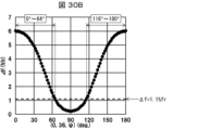
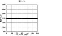
- FIG. 30A is a table showing FEM simulation conditions regarding the LN propagation angle in study example 7.
- FIG. 30B is a graph showing the FEM simulation results regarding the relationship between the LN propagation angle and the fractional bandwidth ⁇ f in Study Example 7.
- FIG. 30C is a graph showing the FEM simulation results regarding the relationship between the LN propagation angle and the sound speed V in Study Example 7.
- the Pt electrode thickness was fixed at 12% ⁇ , which is the center point CP in the above-mentioned FEM simulation results.
- the LN thickness was fixed at 32.5% ⁇ , which is the center point CP in the above-mentioned FEM simulation results, and the LN cut angle was fixed at 36°.
- the fractional bandwidth is It can be seen that ⁇ f is 1.1%fr or more.
- the fitting curve of the plot of the fractional bandwidth ⁇ f shown in FIG. 30B actually has an upwardly convex peak because the LN propagation angles of 0° and 180° are equivalent.
- the maximum point of the fitting curve was selected as the center point CP. That is, the center point CP of the LN propagation angle was set to 0°.
- the main component of the constituent material of the piezoelectric layer 2 is lithium niobate, and the thickness is 7.5% ⁇ or more82. 5% ⁇ . Further, assuming the Euler angles of the piezoelectric layer 2 as ( ⁇ , ⁇ , ⁇ ), ⁇ is -5° or more and 5° or less, ⁇ is -58° or more and 86° or less, and ⁇ is -64° or more and 64° or less. .
- the main component of the constituent material of the IDT electrode 3 is Pt, and the thickness is 0.05% ⁇ or more and 100.0% ⁇ or less.
- the piezoelectric layer 2 may be the same as in the fifth configuration example.
- the IDT electrode 3 may be made of Pt or may be made substantially of Pt.
- the IDT electrode 3 may contain 70% by mass or more of Pt, or may contain 80% by mass or more of Pt.
- the remainder of the constituent material of the IDT electrode 3 other than Pt may consist of arbitrary additive components and unavoidable impurities.
- the center point CP of the Al electrode thickness is 24% ⁇
- the sound velocity (acoustic wave sound speed) V at the center point CP is about 3100 m/s
- the fractional bandwidth ⁇ f at the center point CP. was approximately 4.2 (see Figures 19A-19C).
- the center point CP of the Cu electrode thickness is 18% ⁇
- the sound velocity (acoustic wave sound speed) V at the center point CP is about 2600 m/s
- the specific band at the center point CP The width ⁇ f was approximately 5.3 (see FIGS. 23A-23C).
- the center point CP of the Pt electrode thickness is 12% ⁇
- the sound velocity (acoustic wave sound speed) V at the center point CP is about 2300 m/s
- the fractional bandwidth ⁇ f at the center point CP. was approximately 6.0 (see Figures 27A-27C).
- FIG. 31A is a graph showing the relationship between the transverse sound velocity of the electrode material and the center point CP of the electrode thickness in the results of Study Examples 5 to 7.
- FIG. 31B is a graph showing the relationship between the transverse wave sonic velocity and the sonic velocity (acoustic wave sonic velocity) V of the electrode material in the results of Study Examples 5 to 7.
- FIG. 31C is a graph showing the relationship between the transverse sound velocity of the electrode material and the fractional bandwidth ⁇ f in the results of Study Examples 5 to 7.
- 31A to 31C show straight lines and determination coefficients calculated by approximating the plots corresponding to the results of Study Examples 5 to 7 using linear functions. As shown in FIGS. 31A to 31C, it can be seen that the transverse wave sonic velocity of the electrode material, the sonic velocity (acoustic wave sonic velocity) V, and the fractional bandwidth ⁇ f have a linear function relationship with each other.
- the transverse sound velocity of the electrode material is about 5000 m/s or less, the fractional bandwidth ⁇ f becomes 1.1% fr or more.
- the sound speed of the conventional SAW is about 4000 m/s.
- Conventional SAW includes Rayleigh waves and leaky waves.
- the sound speed of leaky waves propagating through the LT film is approximately 4000 m/s. Therefore, as shown in FIG. 31B, the upper limit of the transverse wave sound speed of the electrode material was set to 4005 m/s as a range in which the sound speed (acoustic wave sound speed) V is slower than that of the conventional SAW. Further, as in Study Example 4 described above, the lower limit of the transverse sound velocity of the electrode material was set to 500 m/s.
- the main component of the constituent material of the piezoelectric layer 2 is lithium niobate, and the thickness is The value is 7.5% ⁇ or more and 92.5% ⁇ or less. Furthermore, assuming the Euler angles of the piezoelectric layer 2 as ( ⁇ , ⁇ , ⁇ ), ⁇ is -5° or more and 5° or less, ⁇ is -58° or more and 90° or less, and ⁇ is -64° or more and 64° or less. .
- the main component of the constituent material of the IDT electrode 3 is a metal having a transverse sound velocity of 500 m/s or more and 4005 m/s or less, and the thickness is 0.05% ⁇ or more and 100.0% ⁇ or less.
- the main component of the constituent material of the piezoelectric layer 2 is lithium niobate.
- the thickness is 10.0% ⁇ or more and 82.5% ⁇ or less.
- the Euler angles of the piezoelectric layer 2 as ( ⁇ , ⁇ , ⁇ ), ⁇ is -5° or more and 5° or less, ⁇ is -38° or more and 84° or less, and ⁇ is -50° or more and 50° or less.
- the main component of the constituent material of the IDT electrode 3 is a metal having a transverse sound velocity of 500 m/s or more and 4005 m/s or less, and the thickness is 0.05% ⁇ or more and 100.0% ⁇ or less.
- the piezoelectric layer 2 may be the same as the above structural example 5.
- the IDT electrode 3 may be made of a metal (hereinafter referred to as "specific metal M2") having a transverse sound velocity of 500 m/s or more and 4005 m/s or less, or may be substantially made of the specific metal M2.
- the main component of the constituent material may be the specific metal M2.
- the relationship between the constituent material of the IDT electrode 3 and the range of the transverse wave sound velocity is the same as that explained in connection with the above-mentioned configuration example 4, and therefore a repeated explanation will be omitted.
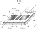
- FIG. 32 is a perspective view showing another structural example of the elastic wave device 100 in this embodiment.
- the elastic wave device 100 in this embodiment may be configured to excite an A0 mode ram wave, and the specific shape of the IDT electrode 3 is not particularly limited.
- the elastic wave device 100 may include a transversal type resonator 1.
- the resonator 1 includes a first IDT electrode 130 (input side IDT electrode) and a second IDT electrode 230 (output side IDT electrode) arranged in the X direction. It's fine.
- the first IDT electrode 130 may have two bus bars 131 (a first bus bar 131a and a second bus bar 131b) facing each other in the y direction.
- the second IDT electrode 230 may include two bus bars 231 (a first bus bar 231a and a second bus bar 231b) facing each other in the y direction.
- the input terminal Tin may be connected to the first bus bar 131a of the first IDT electrode 130
- the output terminal Tout may be connected to the second bus bar 231b of the second IDT electrode 230.
- the second bus bar 131b of the first IDT electrode 130 and the first bus bar 231a of the second IDT electrode 230 may each be connected to a ground terminal.
- the elastic wave device 100 may include the third electrode 14 in the propagation path between the first IDT electrode 130 and the second IDT electrode 230.
- the third electrode 14 may be, for example, an aluminum electrode film, and has a function of improving the propagation efficiency of the signal (A0 mode ram wave) from the first IDT electrode 130 to the second IDT electrode 230.
- the third electrode 14 may or may not be connected to the ground terminal. In the acoustic wave device 100, the third electrode 14 may not be provided.
- each of the first IDT electrode 130 and the second IDT electrode 230 only needs to have the same shape and component ratio as the above-described IDT electrode 3.
- the third electrode 14 a known configuration can be adopted.
- FIG. 33 is a sectional view showing another example of the configuration of the elastic wave device 100 in this embodiment.
- the resonator 1 included in the elastic wave device 100 may have an acoustic reflection film between the support substrate 5 and the piezoelectric layer 2.
- the specific structure of the acoustic reflective film is not particularly limited, for example, the acoustic wave device 100 may have a reflective multilayer film 60 between the support substrate 5 and the piezoelectric layer 2.
- the reflective multilayer film 60 may include a first layer 61 and a second layer 62 which are alternately laminated.
- the constituent material of the first layer 61 may have a lower acoustic impedance than the constituent material of the second layer 62.
- the main component of the first layer 61 may be silicon dioxide (SiO 2 ).
- the main component of the second layer 62 may be hafnium oxide (HfO 2 ).
- the main component of the second layer 62 is tantalum pentoxide (Ta 2 O 5 ), zirconium dioxide (ZrO 2 ), titanium oxide (TiO 2 ), or magnesium oxide (MgO). Good too.
- the reflective multilayer film 60 may include at least one first layer 61 and at least one second layer 62.
- the layer in the reflective multilayer film 60 that is in contact with the piezoelectric layer 2 is the first layer 61 .
- the layer closest to the support substrate 5 in the reflective multilayer film 60 may be either the first layer 61 or the second layer 62.
- the reflective multilayer film 60 may include a total of 3 or more and 12 or less layers, including the first layer 61 and the second layer 62.
- FIG. 34 is a sectional view showing another modification of the elastic wave device 100 in this embodiment.
- the resonator 1 included in the acoustic wave device 100 at least a portion of the IDT electrode 3 may be embedded in the piezoelectric layer 2.
- the upper surface of the electrode finger 32 and the upper surface of the piezoelectric layer 2 are aligned (flush), but the present invention is not limited thereto.
- the IDT electrode 3 may be embedded in the piezoelectric layer 2 such that the upper surface of the electrode finger 32 is convex or concave with respect to the upper surface of the piezoelectric layer 2. Thereby, spurious components can be effectively reduced.
- the resonance frequency of the elastic wave device 100 may be, for example, 700 MHz or more and 900 MHz or less.
- the resonance frequency can be adjusted by changing ⁇ (in other words, the electrode finger pitch p).
- ⁇ is set so that the desired resonance frequency is obtained, and the cross-sectional thicknesses (expressed in % ⁇ ) of the piezoelectric layer 2 and the IDT electrode 3 are calculated based on the set ⁇ .
- the resonator 1 having the piezoelectric layer 2 and the IDT electrode 3 having the calculated thickness may be manufactured.
- FIG. 35 is a diagram illustrating a schematic configuration of the communication device 151.
- the communication device 151 is an application example of the elastic wave device 100 according to one aspect of the present disclosure, and performs wireless communication using radio waves.
- the communication device 151 may include one duplexer 101 as a transmission filter 109 and another duplexer 101 as a reception filter 111.
- Each of the two duplexers 101 may include the elastic wave device 100 according to one aspect of the present disclosure. In this way, the communication device 151 may include the elastic wave device 100 according to one aspect of the present disclosure.
- a transmission information signal TIS containing information to be transmitted is modulated and frequency-increased (converted to a high-frequency signal having a carrier frequency) by an RF-IC (Radio Frequency-Integrated Circuit) 153, and the transmission information signal TIS is converted into a transmission signal. It may be converted to TS.
- the bandpass filter 155 may remove unnecessary components other than the transmission passband for the TS.
- the TS after removing unnecessary components may be amplified by the amplifier 157 and input to the transmission filter 109.
- the transmission filter 109 may remove unnecessary components outside the transmission passband from the input transmission signal TS.
- the transmission filter 109 may output the TS from which unnecessary components have been removed to the antenna 159 via the antenna terminal.
- the antenna 159 may convert the TS, which is an electrical signal input to itself, into a radio wave as a wireless signal, and transmit the radio wave to the outside of the communication device 151.
- the antenna 159 may convert the received radio waves from the outside into a reception signal RS, which is an electrical signal, and input the RS to the reception filter 111 via the antenna terminal.
- the reception filter 111 may remove unnecessary components other than the reception passband from the input RS.
- the reception filter 111 may output the reception signal RS from which unnecessary components have been removed to the amplifier 161.
- the output RS may be amplified by the amplifier 161.
- the bandpass filter 163 may remove unnecessary components other than the receiving passband from the amplified RS.
- the frequency of the RS after unnecessary component removal is lowered and demodulated by the RF-IC 153, and may be converted into a received information signal RIS.
- the TIS and RIS may be low frequency signals (baseband signals) containing appropriate information.
- TIS and RIS may be analog audio signals or digitized audio signals.
- the passband of the wireless signal may be set as appropriate and may conform to various known standards.
Landscapes
- Physics & Mathematics (AREA)
- Acoustics & Sound (AREA)
- Surface Acoustic Wave Elements And Circuit Networks Thereof (AREA)
Abstract
Selon l'invention, un dispositif à ondes élastiques est miniaturisé. Le dispositif à ondes élastiques de l'invention possède : un substrat de support ; une couche piézoélectrique se trouvant en contact direct ou indirect avec le substrat de support ; et une électrode de transducteur interdigital positionnée sur la couche piézoélectrique. En outre, ce dispositif à ondes élastiques excite une onde de Lamb en mode d'ordre zéro asymétrique.
Applications Claiming Priority (2)
| Application Number | Priority Date | Filing Date | Title |
|---|---|---|---|
| JP2022089625 | 2022-06-01 | ||
| JP2022-089625 | 2022-06-01 |
Publications (1)
| Publication Number | Publication Date |
|---|---|
| WO2023234383A1 true WO2023234383A1 (fr) | 2023-12-07 |
Family
ID=89024965
Family Applications (1)
| Application Number | Title | Priority Date | Filing Date |
|---|---|---|---|
| PCT/JP2023/020400 WO2023234383A1 (fr) | 2022-06-01 | 2023-06-01 | Dispositif à ondes élastiques, et dispositif de communication |
Country Status (1)
| Country | Link |
|---|---|
| WO (1) | WO2023234383A1 (fr) |
Citations (5)
| Publication number | Priority date | Publication date | Assignee | Title |
|---|---|---|---|---|
| WO2007046236A1 (fr) * | 2005-10-19 | 2007-04-26 | Murata Manufacturing Co., Ltd. | Dispositif à onde de lamb |
| WO2012086441A1 (fr) * | 2010-12-24 | 2012-06-28 | 株式会社村田製作所 | Dispositif à ondes élastiques et procédé de fabrication correspondant |
| JP2012257019A (ja) * | 2011-06-08 | 2012-12-27 | Murata Mfg Co Ltd | 弾性波装置 |
| WO2013118532A1 (fr) * | 2012-02-06 | 2013-08-15 | 株式会社村田製作所 | Dispositif de filtrage |
| US20210021255A1 (en) * | 2018-03-29 | 2021-01-21 | Frec'n'sys | Surface acoustic wave device on device on composite substrate |
-
2023
- 2023-06-01 WO PCT/JP2023/020400 patent/WO2023234383A1/fr unknown
Patent Citations (5)
| Publication number | Priority date | Publication date | Assignee | Title |
|---|---|---|---|---|
| WO2007046236A1 (fr) * | 2005-10-19 | 2007-04-26 | Murata Manufacturing Co., Ltd. | Dispositif à onde de lamb |
| WO2012086441A1 (fr) * | 2010-12-24 | 2012-06-28 | 株式会社村田製作所 | Dispositif à ondes élastiques et procédé de fabrication correspondant |
| JP2012257019A (ja) * | 2011-06-08 | 2012-12-27 | Murata Mfg Co Ltd | 弾性波装置 |
| WO2013118532A1 (fr) * | 2012-02-06 | 2013-08-15 | 株式会社村田製作所 | Dispositif de filtrage |
| US20210021255A1 (en) * | 2018-03-29 | 2021-01-21 | Frec'n'sys | Surface acoustic wave device on device on composite substrate |
Similar Documents
| Publication | Publication Date | Title |
|---|---|---|
| JP5163746B2 (ja) | 弾性表面波共振子、弾性表面波発振器および弾性表面波モジュール装置 | |
| US9124240B2 (en) | Acoustic wave device and antenna duplexer employing the same | |
| EP1732216B1 (fr) | Dispositif acoustique de surface | |
| CN111587535A (zh) | 弹性波装置、多工器、高频前端电路以及通信装置 | |
| WO2013080461A1 (fr) | Filtre d'onde élastique de type échelle et duplexeur d'antenne utilisant celui-ci | |
| WO2012176455A1 (fr) | Filtre de type itératif à onde élastique et duplexeur d'antenne utilisant celui-ci | |
| US9048813B2 (en) | Acoustic wave device and antenna duplexer using the same | |
| JP2012156741A (ja) | アンテナ共用器 | |
| JP6870684B2 (ja) | マルチプレクサ | |
| JP2003289234A (ja) | 弾性表面波装置、通信装置 | |
| WO2005125005A1 (fr) | Dispositif saw et appareil employant celui-ci | |
| JP7278305B2 (ja) | 弾性波装置、分波器および通信装置 | |
| JP2010011440A (ja) | 弾性波装置及びそれを用いた高周波フィルタ | |
| WO2019022236A1 (fr) | Dispositif à ondes élastiques, duplexeur, et dispositif de communication | |
| CN110710106A (zh) | 弹性波装置、分波器及通信装置 | |
| CN115398801A (zh) | 弹性波谐振器、弹性波滤波器、分波器、通信装置 | |
| JP5163747B2 (ja) | 弾性表面波共振子、弾性表面波発振器および弾性表面波モジュール装置 | |
| US8289107B2 (en) | Acoustic wave device having narrower-pitch electrodes, normally-shaped electrodes and apodized electrodes | |
| WO2023234383A1 (fr) | Dispositif à ondes élastiques, et dispositif de communication | |
| CN112655150A (zh) | 弹性波装置、高频前端电路以及通信装置 | |
| US10483944B2 (en) | Multiplexer | |
| US10998880B2 (en) | Acoustic wave element and communication apparatus | |
| JP5158104B2 (ja) | 弾性表面波共振子、弾性表面波発振器および弾性表面波モジュール装置 | |
| CN110086445B (zh) | 声波器件、滤波器以及复用器 | |
| WO2022025147A1 (fr) | Résonateur à ondes élastiques, filtre à ondes élastiques, démultiplexeur et dispositif de communication |
Legal Events
| Date | Code | Title | Description |
|---|---|---|---|
| 121 | Ep: the epo has been informed by wipo that ep was designated in this application |
Ref document number: 23816140 Country of ref document: EP Kind code of ref document: A1 |