WO2023233651A1 - 直流配電システム及び制御電源生成装置 - Google Patents
直流配電システム及び制御電源生成装置 Download PDFInfo
- Publication number
- WO2023233651A1 WO2023233651A1 PCT/JP2022/022608 JP2022022608W WO2023233651A1 WO 2023233651 A1 WO2023233651 A1 WO 2023233651A1 JP 2022022608 W JP2022022608 W JP 2022022608W WO 2023233651 A1 WO2023233651 A1 WO 2023233651A1
- Authority
- WO
- WIPO (PCT)
- Prior art keywords
- power
- power supply
- voltage
- control
- supplies
- Prior art date
- Legal status (The legal status is an assumption and is not a legal conclusion. Google has not performed a legal analysis and makes no representation as to the accuracy of the status listed.)
- Ceased
Links
Images


Classifications
-
- H—ELECTRICITY
- H02—GENERATION; CONVERSION OR DISTRIBUTION OF ELECTRIC POWER
- H02J—ELECTRIC POWER NETWORKS; CIRCUIT ARRANGEMENTS OR SYSTEMS FOR SUPPLYING OR DISTRIBUTING ELECTRIC POWER; SYSTEMS FOR STORING ELECTRIC ENERGY
- H02J1/00—Circuit arrangements for DC mains or DC distribution networks
- H02J1/10—Parallel operation of DC sources
- H02J1/12—Parallel operation of DC sources having power converters with further DC sources without power converters
-
- H—ELECTRICITY
- H02—GENERATION; CONVERSION OR DISTRIBUTION OF ELECTRIC POWER
- H02J—ELECTRIC POWER NETWORKS; CIRCUIT ARRANGEMENTS OR SYSTEMS FOR SUPPLYING OR DISTRIBUTING ELECTRIC POWER; SYSTEMS FOR STORING ELECTRIC ENERGY
- H02J1/00—Circuit arrangements for DC mains or DC distribution networks
-
- H—ELECTRICITY
- H02—GENERATION; CONVERSION OR DISTRIBUTION OF ELECTRIC POWER
- H02J—ELECTRIC POWER NETWORKS; CIRCUIT ARRANGEMENTS OR SYSTEMS FOR SUPPLYING OR DISTRIBUTING ELECTRIC POWER; SYSTEMS FOR STORING ELECTRIC ENERGY
- H02J1/00—Circuit arrangements for DC mains or DC distribution networks
- H02J1/08—Three-wire DC power distribution systems; Systems having more than three wires
- H02J1/082—DC supplies with two or more different DC voltage levels
-
- H—ELECTRICITY
- H02—GENERATION; CONVERSION OR DISTRIBUTION OF ELECTRIC POWER
- H02J—ELECTRIC POWER NETWORKS; CIRCUIT ARRANGEMENTS OR SYSTEMS FOR SUPPLYING OR DISTRIBUTING ELECTRIC POWER; SYSTEMS FOR STORING ELECTRIC ENERGY
- H02J3/00—Circuit arrangements for AC mains or AC distribution networks
- H02J3/38—Arrangements for feeding a single network from two or more generators or sources in parallel; Arrangements for feeding already energised networks from additional generators or sources in parallel
- H02J3/381—Dispersed generators
-
- H—ELECTRICITY
- H02—GENERATION; CONVERSION OR DISTRIBUTION OF ELECTRIC POWER
- H02J—ELECTRIC POWER NETWORKS; CIRCUIT ARRANGEMENTS OR SYSTEMS FOR SUPPLYING OR DISTRIBUTING ELECTRIC POWER; SYSTEMS FOR STORING ELECTRIC ENERGY
- H02J7/00—Circuit arrangements for charging or discharging batteries or for supplying loads from batteries
- H02J7/34—Parallel operation in networks using both storage and other DC sources, e.g. providing buffering
- H02J7/35—Parallel operation in networks using both storage and other DC sources, e.g. providing buffering with light sensitive cells
-
- H—ELECTRICITY
- H02—GENERATION; CONVERSION OR DISTRIBUTION OF ELECTRIC POWER
- H02M—APPARATUS FOR CONVERSION BETWEEN AC AND AC, BETWEEN AC AND DC, OR BETWEEN DC AND DC, AND FOR USE WITH MAINS OR SIMILAR POWER SUPPLY SYSTEMS; CONVERSION OF DC OR AC INPUT POWER INTO SURGE OUTPUT POWER; CONTROL OR REGULATION THEREOF
- H02M1/00—Details of apparatus for conversion
- H02M1/0003—Details of control, feedback or regulation circuits
- H02M1/0006—Arrangements for supplying an adequate voltage to the control circuit of converters
-
- H—ELECTRICITY
- H02—GENERATION; CONVERSION OR DISTRIBUTION OF ELECTRIC POWER
- H02M—APPARATUS FOR CONVERSION BETWEEN AC AND AC, BETWEEN AC AND DC, OR BETWEEN DC AND DC, AND FOR USE WITH MAINS OR SIMILAR POWER SUPPLY SYSTEMS; CONVERSION OF DC OR AC INPUT POWER INTO SURGE OUTPUT POWER; CONTROL OR REGULATION THEREOF
- H02M3/00—Conversion of DC power input into DC power output
- H02M3/02—Conversion of DC power input into DC power output without intermediate conversion into AC
- H02M3/04—Conversion of DC power input into DC power output without intermediate conversion into AC by static converters
- H02M3/10—Conversion of DC power input into DC power output without intermediate conversion into AC by static converters using discharge tubes with control electrode or semiconductor devices with control electrode
- H02M3/145—Conversion of DC power input into DC power output without intermediate conversion into AC by static converters using discharge tubes with control electrode or semiconductor devices with control electrode using devices of a triode or transistor type requiring continuous application of a control signal
- H02M3/155—Conversion of DC power input into DC power output without intermediate conversion into AC by static converters using discharge tubes with control electrode or semiconductor devices with control electrode using devices of a triode or transistor type requiring continuous application of a control signal using semiconductor devices only
- H02M3/156—Conversion of DC power input into DC power output without intermediate conversion into AC by static converters using discharge tubes with control electrode or semiconductor devices with control electrode using devices of a triode or transistor type requiring continuous application of a control signal using semiconductor devices only with automatic control of output voltage or current, e.g. switching regulators
- H02M3/158—Conversion of DC power input into DC power output without intermediate conversion into AC by static converters using discharge tubes with control electrode or semiconductor devices with control electrode using devices of a triode or transistor type requiring continuous application of a control signal using semiconductor devices only with automatic control of output voltage or current, e.g. switching regulators including plural semiconductor devices as final control devices for a single load
-
- H—ELECTRICITY
- H02—GENERATION; CONVERSION OR DISTRIBUTION OF ELECTRIC POWER
- H02J—ELECTRIC POWER NETWORKS; CIRCUIT ARRANGEMENTS OR SYSTEMS FOR SUPPLYING OR DISTRIBUTING ELECTRIC POWER; SYSTEMS FOR STORING ELECTRIC ENERGY
- H02J2101/00—Supply or distribution of decentralised, dispersed or local electric power generation
- H02J2101/20—Dispersed power generation using renewable energy sources
- H02J2101/22—Solar energy
- H02J2101/24—Photovoltaics
Definitions
- the present application relates to a DC power distribution system and a controlled power generation device.
- a DC/DC converter is used as a control power source for a voltage type inverter, and its input power is supplied from both an AC power source and a DC voltage of the inverter or an external DC power source.
- the power supply circuit shown in Patent Document 1 provides a separate capacitor for the DC/DC converter input, and charges this capacitor from an AC power supply via a relay contact and a rectifier, or charges this capacitor from the DC voltage of an inverter. It is configured so that it can be charged either by That is, the DC voltage of the inverter is detected by charging from the DC voltage of the inverter while the inverter is in operation, and by charging from the AC power source when the inverter is stopped.
- the present invention provides a DC power distribution system and a control power generation device that enable the system to continue operating even in the event of an abnormality due to equipment failure or power outage, and that suppress power consumption of the control power source in response to voltage fluctuations of the power supply source.
- the DC power distribution system disclosed in this application is one in which a power distribution network is formed that supplies power from multiple power supply sources to multiple electrical loads, and is connected between the multiple power supply sources and the multiple electrical loads.
- the control power generation unit detects each power supply source and includes a power conversion circuit that is connected to the power conversion circuit and supplies power according to the electric load, and a control power generation unit that supplies control power for controlling the power conversion circuit.
- a control device that inputs the detected voltage and sets a voltage command value according to the detected voltage when the input detected voltage is larger than a predetermined value is connected to each power supply source and outputs the voltage command.
- a control device comprising: a plurality of power supply circuits that output a DC voltage converted according to a value; and a control power supply circuit that supplies a control power supply to a power conversion circuit based on one of the outputs of the plurality of power supply circuits; is characterized in that the voltage command value corresponding to the lowest voltage among the detected voltages larger than a predetermined value is set to the largest value.
- voltage command values are set according to voltage fluctuations of a plurality of power supply sources, and outputs of a plurality of power supply circuits output DC voltages converted according to the voltage command values.
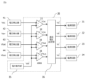
- FIG. 1 is an overall configuration diagram of a DC power distribution system according to Embodiment 1.
- FIG. 1 is a diagram showing an outline of a DC/DC converter circuit of a power conversion device according to a first embodiment
- FIG. 1 is a functional block diagram of a control device according to Embodiment 1.
- FIG. 2 is a diagram showing a magnitude relationship of power supply voltages of the power supply source in FIG. 1
- FIG. 3 is a diagram illustrating selection of a maximum voltage according to the first embodiment.
- 3 is a circuit diagram showing an example of a power supply circuit in Embodiment 1.
- FIG. 7 is a circuit diagram showing an example of a power supply circuit in Embodiment 2.
- FIG. FIG. 3 is an overall configuration diagram of a DC power distribution system according to a third embodiment.
- FIG. 3 is a functional block diagram of a control device according to Embodiment 3.
- FIG. 7 is a time chart showing the magnitude relationship of the power supply voltage and the operation of the open/close switch in Embodiment 3.
- FIG. 3 is a diagram showing an example of the hardware configuration of a DC voltage setting section and a control section.
- FIG. 1 is an overall configuration diagram of a DC power distribution system according to a first embodiment.
- the DC power distribution system includes a power converter 10 connected between a plurality of power supply sources such as a grid power supply 1, a solar cell 2, and a storage battery 3 and a plurality of electric loads 4 to 6;
- the power conversion device 10 is connected between the grid power supply 1 and the DC bus circuit 17, and is equipped with a control power generation unit 20 that supplies a control power supply.
- a bidirectional AC/DC converter circuit 11 that performs bidirectional conversion, a DC/DC converter circuit 12 that is connected between the solar cell 2 of the plurality of power sources and the DC bus circuit 17 and converts DC power, and a plurality of DC/DC converter circuits 12 that convert DC power.
- a charging/discharging circuit 13 is connected between the storage battery 3 and the DC bus circuit 17 and charges and discharges the storage battery 3
- a charging/discharging circuit 13 is connected between the DC bus circuit 17 and the plurality of electrical loads 4 to 6, It has DC/DC converter circuits 14 to 16 that convert the DC power of the DC bus line 17.
- FIG. 2 specifically shows an outline of each DC/DC converter circuit of the power conversion device 10. Note that the connection between the controlled power generation unit 20 and the power conversion device 10 is omitted. Note that the circuit configuration of the power conversion device 10 in the second and third embodiments is the same as that in FIG. 2.
- the control power generation unit 20 receives as input the voltage Vac obtained from the grid power supply 1, the voltage Vpv obtained from the solar cell 2, the voltage Vbat obtained from the storage battery 3, and the voltage Vbus obtained from the DC bus circuit 17. , power supply circuits 21 to 24 that convert each input voltage into a desired DC voltage according to the voltage command value calculated by the control device 30. The respective outputs of the power supply circuits 21 to 24 are matched by diodes and then inputted to a control power supply circuit 25 which outputs the control power supply Vdc.
- FIG. 3 is a functional block diagram of the control device 30 in FIG. 1.
- the control device 30 detects the voltage Vac obtained from the system power supply 1 by the voltage detector 41, the voltage Vpv obtained from the solar cell 2 by the voltage detector 42, the voltage Vbat obtained from the storage battery 3 by the voltage detector 43, and the voltage Subtractors 31 to 34 which input the voltage Vbus obtained from the DC bus circuit 17 by the detector 44 and subtract the voltage command value Vdc* output from the voltage command unit 35 from the respective inputs;
- the DC voltage setting unit 36 outputs voltage command values Va* to Vd* to the power supply circuits 21 to 24 in accordance with the output of the DC voltage setting unit 36.
- FIG. 4 is a diagram showing the magnitude relationship of the power supply voltages of the power supply sources of FIG. 1.
- the peak voltage of the voltage Vac is approximately 565V.
- the operation will be described when the voltage Vpv obtained from the solar cell 2 is 230V DC, the DC voltage Vbat of the storage battery 3 is 266V DC, and the DC voltage Vbus of the DC bus circuit 17 is 690V DC.
- FIG. 5 is a diagram illustrating selection of the maximum voltage.
- FIG. 5A is a flowchart for selecting the maximum voltage
- FIGS. 5B and 5C are conceptual diagrams showing a procedure for arranging input values.
- the control device 30 shown in FIG. Vbat and the voltage Vbus obtained from the DC bus circuit 17 by the voltage detector 44 are respectively input, and the voltage command value Vdc* output from the voltage command section 35 is subtracted by the subtractors 31 to 34.
- each voltage has the following relationship.
- V'ac Vac-Vdc*
- V'pv Vpv-Vdc*
- V'bat Vbat-Vdc*
- V'bus Vbus-Vdc*
- the DC voltage setting unit 36 counts input values that are positive numbers among the voltages V'ac, V'pv, V'bat, and V'bus (step S100). As shown in FIG. 4A, since the voltages Vac, Vpv, Vbat, and Vbus are all larger than the voltage command value Vdc*, the voltages V'ac, V'pv, V'bat, and V' are obtained by subtracting the voltage command value Vdc*. All buses are counted as positive values.
- step S110 one maximum value is selected from the unsorted positive input values (step S110), and the positive input values are sorted in descending order (step S120).
- V'bus since the voltage V'bus is the maximum value, V'ac and V'bus are exchanged to make this value the first value.
- the exchanged V'ac and V'pv are compared, and if V'ac is larger, V'ac and V'pv are exchanged. In this way, comparison calculations are performed until all the counted positive input values are aligned (step S130).
- the DC voltage setting unit 36 sends the voltage command value Va* to the power supply circuit 21, the voltage command value Vb* to the power supply circuit 22, the voltage command value Vc* to the power supply circuit 23, The voltage command value Vd* is outputted to the power supply circuit 24, respectively.
- the voltage command value is set to have a magnitude relationship as shown by (Equation 2) below. That is, the voltage command value Vb* is set so that the difference V[4] (see FIG. 4A) between the selected V'pv and the voltage command value Vb* is the smallest.
- each voltage command value is set so that the difference V[i] between the aligned input values and the voltage command value is small (step S140), and (Formula 2) is obtained. .
- the outputs of the power supply circuits 21 to 24 are matched by diodes, and the output voltage Vb of the power supply circuit 22 is input to the control power supply circuit 25 from the relationship of (Equation 2).
- FIG. 4B the operation will be described when the voltage Vpv obtained from the solar cell 2 is set to DC175V due to changes in the weather environment such as the amount of solar radiation.
- the DC voltage setting unit 36 counts positive input values among V'ac, V'pv, V'bat, and V'bus (step S100). In this case, since V'pv is a negative value, it is excluded from the alignment targets.
- V'ac is the maximum value
- V'ac and V'bus are exchanged to make this value the first value.
- the replaced V'ac and V'bat are compared, and if V'ac is larger, V'ac and V'bat are replaced. In this way, comparison calculations are performed until all the counted input values are aligned (step S130).
- the DC voltage setting unit 36 sends a voltage command value Va* to the power supply circuit 21, a stop command to the power supply circuit 22, a voltage command value Vc* to the power supply circuit 23, and a voltage command value Va* to the power supply circuit 22.
- the voltage command value Vd* is outputted to 24, respectively.
- the voltage command value is set to have a magnitude relationship as shown by the following equation (4). That is, the voltage command value Vc* is set so that the difference V[3] (see FIG. 4B) between the selected V'bat and the voltage command value Vc* is the smallest.
- the outputs of the power supply circuits 21 to 24 are matched by diodes, and the output voltage Vc of the power supply circuit 22 is inputted to the control power supply circuit 25 from the relationship of (Equation 4).
- the magnitude relationship of the voltage values is arranged in descending order so that the control device 30 can recognize it, and the control device 30 maintains the magnitude relationship of the voltage values, so that Vpv Even if Vac disappears, another power supply source can be immediately selected, and it is possible to suppress power consumption of the control power source without stopping the system due to voltage fluctuations of the power supply source.
- FIG. 6 is a circuit diagram showing an example of the power supply circuits 21 and 22 provided in the control power generation section 20.
- the power supply circuit 21 receives the voltage Vac obtained from the system power supply 1
- the power supply circuit 22 receives the voltage Vpv obtained from the solar cell 2, respectively, and constitutes a DC/DC converter circuit that can be electrically isolated from the output voltage. There is.
- the output voltage Va can be adjusted by receiving the voltage command value Va* output from the DC voltage setting unit 36 and making the resistance value of the resistor R11 shown in (Equation 5) variable.
- the power supply circuit 22 shown in FIG. 6 similarly has an output voltage setting section 221. Furthermore, although not shown in FIG. 6, the power supply circuit 23 and the power supply circuit 24 are similarly configured, and the output voltage according to the voltage command value can be adjusted by the voltage setting section each has.
- Embodiment 1 by generating the control power for the DC power distribution system from multiple power supply sources, the system can continue to operate even in the event of an abnormality due to equipment failure or power outage, and the power supply circuit Since a power supply source with a small input-output difference is selected, power consumption of the control power source can be suppressed against voltage fluctuations of the power supply source.
- this embodiment shows a configuration in which three electrical loads are connected to the DC power distribution system, it goes without saying that the same effect can be obtained even if the number of electrical loads is further increased.
- FIG. 7 shows another example of the power supply circuit provided in the control power generation section 20.
- the power supply circuit 21a and the power supply circuit 22a respectively input the voltage Vac obtained from the system power supply 1 and the voltage Vpv obtained from the solar cell 2, and constitute a DC/DC converter circuit that can be electrically isolated from the output voltage. There is.
- the output stage of the power supply circuit 21a has an output voltage setting section 211a consisting of a shunt regulator IC1, a plurality of resistors R11, R12, R13, and an on/off switch S1. Switch between conductive state and open state.
- the power supply circuit 22a shown in FIG. 7 similarly has an output voltage setting section 221a.
- other power supply circuits that is, a power supply circuit whose input is the voltage Vbat obtained from the storage battery 3, and a power supply circuit whose input is Vbus obtained from the DC bus circuit 17, are configured in the same manner. You can leave it there.
- the output voltage of each power supply circuit changes according to (Equation 6) or (Equation 7) by switching the open/close switch between the conductive state and the open state.
- control power for a DC power distribution system is generated from a plurality of power supply sources, and a shunt regulator and a plurality of resistors are connected to the output of each power supply circuit provided in the control power generation section 20.
- the output voltage setting sections 211a and 221a each of which includes an open/close switch, the output voltages of the plurality of power supply circuits can be switched. Therefore, the system can continue to operate even in the event of an abnormality due to equipment failure or power outage, and the power required for the control power source can be selected from a desired power supply source.
- the open/close switches S1 and S2 are illustrated as switches that move mechanically, but the same effect can be obtained even if an electrical semiconductor switch is used to switch between a conductive state and an open state. Needless to say, it can be done. Note that by increasing the number of resistors to be switched, switching similar to that of the variable resistor shown in Embodiment 1 can be achieved.
- FIG. 8 is an overall configuration diagram of a DC power distribution system according to Embodiment 3.
- the DC power distribution system includes a power converter 10 connected between a plurality of power supply sources such as a grid power supply 1, a solar cell 2, and a storage battery 3, and a plurality of electric loads 4 to 6. It has a control power generation section 20A that supplies control power to a plurality of circuits built into the controller.
- the controlled power generation unit 20A receives as input the voltage Vac obtained from the system power supply 1, the voltage Vpv obtained from the solar cell 2, the voltage Vbat obtained from the storage battery 3, and the voltage Vbus obtained from the DC bus circuit 17, and generates a voltage Vac obtained from the power supply system 1, which is set in advance.
- the outputs of the power supply circuits 21 to 24 include a plurality of DC/DC converter circuits 12, 14 to 16 built into the power conversion device 10, and a bidirectional AC/DC converter circuit. 11, and open/close switches 26 to 29 for switching the electrical circuit that supplies control power to the charging/discharging circuit 13 between a conductive state and an open state.
- FIG. 9 is a functional block diagram of a control device 30A according to the third embodiment.
- the control device 30A detects the voltage Vac obtained from the system power supply 1 by the voltage detector 41, the voltage Vpv obtained from the solar cell 2 by the voltage detector 42, the voltage Vbat obtained from the storage battery 3 by the voltage detector 43, and the voltage Subtractors 31a to 34a that receive the voltage Vbus obtained from the DC bus circuit 17 by the detector 44 and subtract the voltage command value Vdc* output from the voltage command unit 35 from the respective inputs; and the on/off switches 26 to 29.
- the control section 37 outputs a signal for switching between a conductive state and an open state.
- FIG. 10 is a time chart showing the magnitude relationship of the power supply voltage and the operation of the open/close switch according to the third embodiment.
- the on-off switch 27 is opened and the on-off switch 28 is made conductive.
- the control power source Vdc can be obtained from the voltage Vbat obtained from the storage battery 3 which is larger than the voltage command value Vdc* and has the smallest voltage difference.
- the control power supply for the system is generated from a plurality of power supply sources, and the output of the power supply circuit outputs a preset control power supply Vdc.
- the system can continue to operate even in the event of an abnormality due to equipment failure or power outage, while also reducing the input/output difference in the power supply circuit. Since a power supply source with a small value is selected, power consumption of the control power source can be suppressed against voltage fluctuations of the power supply source.
- the opening/closing switch is illustrated as a switch that moves mechanically, but the same effect can be obtained even if an electrical semiconductor switch is used to switch between the conductive state and the open state. Needless to say.
- the DC voltage setting section 36 of the first embodiment and the control section 37 of the third embodiment may be configured of a processor 100 and a storage device 101, as an example of hardware shown in FIG.
- the storage device 101 includes a volatile storage device such as a random access memory, and a nonvolatile auxiliary storage device such as a flash memory. Further, an auxiliary storage device such as a hard disk may be provided instead of the flash memory.
- a processor 100 a CPU (Central Processing Unit), an ASIC (Application Specific Integrated Circuit), an IC (Integrated Circuit), an FPGA ( Field Programmable Gate Array), various logic circuits, and various signal processing circuits, etc. good.
- a plurality of processors of the same type or different types may be provided as the processor 100, and each process may be shared and executed.
Landscapes
- Engineering & Computer Science (AREA)
- Power Engineering (AREA)
- Charge And Discharge Circuits For Batteries Or The Like (AREA)
- Direct Current Feeding And Distribution (AREA)
Priority Applications (3)
| Application Number | Priority Date | Filing Date | Title |
|---|---|---|---|
| JP2024524130A JP7706656B2 (ja) | 2022-06-03 | 2022-06-03 | 直流配電システム及び制御電源生成装置 |
| US18/863,489 US20250300456A1 (en) | 2022-06-03 | 2022-06-03 | Dc power distribution system and control power generation device |
| PCT/JP2022/022608 WO2023233651A1 (ja) | 2022-06-03 | 2022-06-03 | 直流配電システム及び制御電源生成装置 |
Applications Claiming Priority (1)
| Application Number | Priority Date | Filing Date | Title |
|---|---|---|---|
| PCT/JP2022/022608 WO2023233651A1 (ja) | 2022-06-03 | 2022-06-03 | 直流配電システム及び制御電源生成装置 |
Publications (1)
| Publication Number | Publication Date |
|---|---|
| WO2023233651A1 true WO2023233651A1 (ja) | 2023-12-07 |
Family
ID=89026171
Family Applications (1)
| Application Number | Title | Priority Date | Filing Date |
|---|---|---|---|
| PCT/JP2022/022608 Ceased WO2023233651A1 (ja) | 2022-06-03 | 2022-06-03 | 直流配電システム及び制御電源生成装置 |
Country Status (3)
| Country | Link |
|---|---|
| US (1) | US20250300456A1 (https=) |
| JP (1) | JP7706656B2 (https=) |
| WO (1) | WO2023233651A1 (https=) |
Citations (4)
| Publication number | Priority date | Publication date | Assignee | Title |
|---|---|---|---|---|
| JPS62239863A (ja) * | 1986-04-10 | 1987-10-20 | Nec Corp | 電源多重化冗長運転方式 |
| JP2011097818A (ja) * | 2009-10-02 | 2011-05-12 | Panasonic Electric Works Co Ltd | 配電システム |
| JP2017085780A (ja) * | 2015-10-28 | 2017-05-18 | 三菱電機株式会社 | 直流給電システム |
| WO2019130375A1 (ja) * | 2017-12-25 | 2019-07-04 | 三菱電機株式会社 | 電力変換装置 |
Family Cites Families (7)
| Publication number | Priority date | Publication date | Assignee | Title |
|---|---|---|---|---|
| JP4515573B2 (ja) * | 1999-12-20 | 2010-08-04 | 澤藤電機株式会社 | 振動型圧縮機の駆動装置 |
| US20140077608A1 (en) * | 2012-09-18 | 2014-03-20 | Panasonic Corporation | Power generation control device, photovoltaic power generation system and power generation control method |
| CN108883787B (zh) * | 2016-04-08 | 2021-03-26 | 三菱电机株式会社 | 电动助力转向装置 |
| JP6774312B2 (ja) * | 2016-11-21 | 2020-10-21 | 株式会社東芝 | 電源装置、電源システム、センサシステムおよび方法 |
| US11557796B2 (en) * | 2019-07-23 | 2023-01-17 | Cummins Inc. | DC-DC-converter-based active voltage-balancing system and method for parallel battery packs |
| JP2021100297A (ja) * | 2019-12-20 | 2021-07-01 | キヤノン株式会社 | 電源装置及びシステム |
| US11764679B2 (en) * | 2020-01-15 | 2023-09-19 | Solaredge Technologies Ltd. | Power device |
-
2022
- 2022-06-03 JP JP2024524130A patent/JP7706656B2/ja active Active
- 2022-06-03 WO PCT/JP2022/022608 patent/WO2023233651A1/ja not_active Ceased
- 2022-06-03 US US18/863,489 patent/US20250300456A1/en active Pending
Patent Citations (4)
| Publication number | Priority date | Publication date | Assignee | Title |
|---|---|---|---|---|
| JPS62239863A (ja) * | 1986-04-10 | 1987-10-20 | Nec Corp | 電源多重化冗長運転方式 |
| JP2011097818A (ja) * | 2009-10-02 | 2011-05-12 | Panasonic Electric Works Co Ltd | 配電システム |
| JP2017085780A (ja) * | 2015-10-28 | 2017-05-18 | 三菱電機株式会社 | 直流給電システム |
| WO2019130375A1 (ja) * | 2017-12-25 | 2019-07-04 | 三菱電機株式会社 | 電力変換装置 |
Also Published As
| Publication number | Publication date |
|---|---|
| JP7706656B2 (ja) | 2025-07-11 |
| JPWO2023233651A1 (https=) | 2023-12-07 |
| US20250300456A1 (en) | 2025-09-25 |
Similar Documents
| Publication | Publication Date | Title |
|---|---|---|
| US9240685B2 (en) | Reconfigurable matrix-based power distribution architecture | |
| JP4819762B2 (ja) | 給電システムおよび給電システムの制御方法 | |
| US9641005B2 (en) | Electric power supply system | |
| US10784713B2 (en) | Uninterruptible power supply device | |
| US9876438B2 (en) | Converter unit system having inrush-current suppression circuit | |
| JP7228949B2 (ja) | 電力変換装置 | |
| TWI593213B (zh) | 不斷電電源裝置 | |
| US10177586B2 (en) | Electric energy storage apparatus | |
| JP4586204B2 (ja) | 太陽光発電システム | |
| US20100013314A1 (en) | Extending backup times of uninterruptible power supplies | |
| JP7618660B2 (ja) | エネルギー生成システムを動作させるための方法、および前記方法を含むエネルギー生成システム | |
| JP2017085780A (ja) | 直流給電システム | |
| JP6316152B2 (ja) | パワーコンディショナ | |
| CN107820670A (zh) | 电力转换装置的控制装置 | |
| JP7126243B2 (ja) | 電力供給システム | |
| JP2017118598A (ja) | 電力供給システム | |
| JP7299095B2 (ja) | 無停電電源装置 | |
| WO2023233651A1 (ja) | 直流配電システム及び制御電源生成装置 | |
| JP6141227B2 (ja) | パワーコンディショナ | |
| EP1513240A2 (en) | Apparatus for supplying standby power | |
| JP5890341B2 (ja) | 蓄電装置 | |
| WO2017038787A1 (ja) | 電源装置 | |
| US12266921B2 (en) | Installation including a stored energy source and an electric motor which can be fed by an inverter, and method for operating an installation | |
| JP7835107B2 (ja) | 電力変換装置、電力供給システム及び制御方法 | |
| JP6552973B2 (ja) | 切替回路及び電源システム |
Legal Events
| Date | Code | Title | Description |
|---|---|---|---|
| 121 | Ep: the epo has been informed by wipo that ep was designated in this application |
Ref document number: 22944931 Country of ref document: EP Kind code of ref document: A1 |
|
| WWE | Wipo information: entry into national phase |
Ref document number: 18863489 Country of ref document: US |
|
| WWE | Wipo information: entry into national phase |
Ref document number: 2024524130 Country of ref document: JP |
|
| NENP | Non-entry into the national phase |
Ref country code: DE |
|
| 122 | Ep: pct application non-entry in european phase |
Ref document number: 22944931 Country of ref document: EP Kind code of ref document: A1 |
|
| WWP | Wipo information: published in national office |
Ref document number: 18863489 Country of ref document: US |