WO2023233651A1 - Dc power distribution system and control power supply generation device - Google Patents
Dc power distribution system and control power supply generation device Download PDFInfo
- Publication number
- WO2023233651A1 WO2023233651A1 PCT/JP2022/022608 JP2022022608W WO2023233651A1 WO 2023233651 A1 WO2023233651 A1 WO 2023233651A1 JP 2022022608 W JP2022022608 W JP 2022022608W WO 2023233651 A1 WO2023233651 A1 WO 2023233651A1
- Authority
- WO
- WIPO (PCT)
- Prior art keywords
- power
- power supply
- voltage
- control
- supplies
- Prior art date
Links
- 238000006243 chemical reaction Methods 0.000 claims abstract description 24
- 238000010248 power generation Methods 0.000 claims description 23
- 230000004044 response Effects 0.000 claims description 3
- 238000001514 detection method Methods 0.000 claims 3
- 230000002159 abnormal effect Effects 0.000 abstract 1
- 238000010586 diagram Methods 0.000 description 18
- 230000005856 abnormality Effects 0.000 description 5
- 230000002457 bidirectional effect Effects 0.000 description 5
- 239000003990 capacitor Substances 0.000 description 4
- 238000007599 discharging Methods 0.000 description 4
- 230000000694 effects Effects 0.000 description 4
- 230000005855 radiation Effects 0.000 description 3
- 238000000034 method Methods 0.000 description 2
- 239000004065 semiconductor Substances 0.000 description 2
- 238000005516 engineering process Methods 0.000 description 1
- 230000006870 function Effects 0.000 description 1
Images


Classifications
-
- H—ELECTRICITY
- H02—GENERATION; CONVERSION OR DISTRIBUTION OF ELECTRIC POWER
- H02J—CIRCUIT ARRANGEMENTS OR SYSTEMS FOR SUPPLYING OR DISTRIBUTING ELECTRIC POWER; SYSTEMS FOR STORING ELECTRIC ENERGY
- H02J1/00—Circuit arrangements for dc mains or dc distribution networks
Definitions
- the present application relates to a DC power distribution system and a controlled power generation device.
- a DC/DC converter is used as a control power source for a voltage type inverter, and its input power is supplied from both an AC power source and a DC voltage of the inverter or an external DC power source.
- the power supply circuit shown in Patent Document 1 provides a separate capacitor for the DC/DC converter input, and charges this capacitor from an AC power supply via a relay contact and a rectifier, or charges this capacitor from the DC voltage of an inverter. It is configured so that it can be charged either by That is, the DC voltage of the inverter is detected by charging from the DC voltage of the inverter while the inverter is in operation, and by charging from the AC power source when the inverter is stopped.
- the present invention provides a DC power distribution system and a control power generation device that enable the system to continue operating even in the event of an abnormality due to equipment failure or power outage, and that suppress power consumption of the control power source in response to voltage fluctuations of the power supply source.
- the DC power distribution system disclosed in this application is one in which a power distribution network is formed that supplies power from multiple power supply sources to multiple electrical loads, and is connected between the multiple power supply sources and the multiple electrical loads.
- the control power generation unit detects each power supply source and includes a power conversion circuit that is connected to the power conversion circuit and supplies power according to the electric load, and a control power generation unit that supplies control power for controlling the power conversion circuit.
- a control device that inputs the detected voltage and sets a voltage command value according to the detected voltage when the input detected voltage is larger than a predetermined value is connected to each power supply source and outputs the voltage command.
- a control device comprising: a plurality of power supply circuits that output a DC voltage converted according to a value; and a control power supply circuit that supplies a control power supply to a power conversion circuit based on one of the outputs of the plurality of power supply circuits; is characterized in that the voltage command value corresponding to the lowest voltage among the detected voltages larger than a predetermined value is set to the largest value.
- voltage command values are set according to voltage fluctuations of a plurality of power supply sources, and outputs of a plurality of power supply circuits output DC voltages converted according to the voltage command values.
- FIG. 1 is an overall configuration diagram of a DC power distribution system according to Embodiment 1.
- FIG. 1 is a diagram showing an outline of a DC/DC converter circuit of a power conversion device according to a first embodiment
- FIG. 1 is a functional block diagram of a control device according to Embodiment 1.
- FIG. 2 is a diagram showing a magnitude relationship of power supply voltages of the power supply source in FIG. 1
- FIG. 3 is a diagram illustrating selection of a maximum voltage according to the first embodiment.
- 3 is a circuit diagram showing an example of a power supply circuit in Embodiment 1.
- FIG. 7 is a circuit diagram showing an example of a power supply circuit in Embodiment 2.
- FIG. FIG. 3 is an overall configuration diagram of a DC power distribution system according to a third embodiment.
- FIG. 3 is a functional block diagram of a control device according to Embodiment 3.
- FIG. 7 is a time chart showing the magnitude relationship of the power supply voltage and the operation of the open/close switch in Embodiment 3.
- FIG. 3 is a diagram showing an example of the hardware configuration of a DC voltage setting section and a control section.
- FIG. 1 is an overall configuration diagram of a DC power distribution system according to a first embodiment.
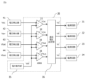
- the DC power distribution system includes a power converter 10 connected between a plurality of power supply sources such as a grid power supply 1, a solar cell 2, and a storage battery 3 and a plurality of electric loads 4 to 6;
- the power conversion device 10 is connected between the grid power supply 1 and the DC bus circuit 17, and is equipped with a control power generation unit 20 that supplies a control power supply.
- a bidirectional AC/DC converter circuit 11 that performs bidirectional conversion, a DC/DC converter circuit 12 that is connected between the solar cell 2 of the plurality of power sources and the DC bus circuit 17 and converts DC power, and a plurality of DC/DC converter circuits 12 that convert DC power.
- a charging/discharging circuit 13 is connected between the storage battery 3 and the DC bus circuit 17 and charges and discharges the storage battery 3
- a charging/discharging circuit 13 is connected between the DC bus circuit 17 and the plurality of electrical loads 4 to 6, It has DC/DC converter circuits 14 to 16 that convert the DC power of the DC bus line 17.
- FIG. 2 specifically shows an outline of each DC/DC converter circuit of the power conversion device 10. Note that the connection between the controlled power generation unit 20 and the power conversion device 10 is omitted. Note that the circuit configuration of the power conversion device 10 in the second and third embodiments is the same as that in FIG. 2.
- the control power generation unit 20 receives as input the voltage Vac obtained from the grid power supply 1, the voltage Vpv obtained from the solar cell 2, the voltage Vbat obtained from the storage battery 3, and the voltage Vbus obtained from the DC bus circuit 17. , power supply circuits 21 to 24 that convert each input voltage into a desired DC voltage according to the voltage command value calculated by the control device 30. The respective outputs of the power supply circuits 21 to 24 are matched by diodes and then inputted to a control power supply circuit 25 which outputs the control power supply Vdc.
- FIG. 3 is a functional block diagram of the control device 30 in FIG. 1.
- the control device 30 detects the voltage Vac obtained from the system power supply 1 by the voltage detector 41, the voltage Vpv obtained from the solar cell 2 by the voltage detector 42, the voltage Vbat obtained from the storage battery 3 by the voltage detector 43, and the voltage Subtractors 31 to 34 which input the voltage Vbus obtained from the DC bus circuit 17 by the detector 44 and subtract the voltage command value Vdc* output from the voltage command unit 35 from the respective inputs;
- the DC voltage setting unit 36 outputs voltage command values Va* to Vd* to the power supply circuits 21 to 24 in accordance with the output of the DC voltage setting unit 36.
- FIG. 4 is a diagram showing the magnitude relationship of the power supply voltages of the power supply sources of FIG. 1.
- the peak voltage of the voltage Vac is approximately 565V.
- the operation will be described when the voltage Vpv obtained from the solar cell 2 is 230V DC, the DC voltage Vbat of the storage battery 3 is 266V DC, and the DC voltage Vbus of the DC bus circuit 17 is 690V DC.
- FIG. 5 is a diagram illustrating selection of the maximum voltage.
- FIG. 5A is a flowchart for selecting the maximum voltage
- FIGS. 5B and 5C are conceptual diagrams showing a procedure for arranging input values.
- the control device 30 shown in FIG. Vbat and the voltage Vbus obtained from the DC bus circuit 17 by the voltage detector 44 are respectively input, and the voltage command value Vdc* output from the voltage command section 35 is subtracted by the subtractors 31 to 34.
- each voltage has the following relationship.
- V'ac Vac-Vdc*
- V'pv Vpv-Vdc*
- V'bat Vbat-Vdc*
- V'bus Vbus-Vdc*
- the DC voltage setting unit 36 counts input values that are positive numbers among the voltages V'ac, V'pv, V'bat, and V'bus (step S100). As shown in FIG. 4A, since the voltages Vac, Vpv, Vbat, and Vbus are all larger than the voltage command value Vdc*, the voltages V'ac, V'pv, V'bat, and V' are obtained by subtracting the voltage command value Vdc*. All buses are counted as positive values.
- step S110 one maximum value is selected from the unsorted positive input values (step S110), and the positive input values are sorted in descending order (step S120).
- V'bus since the voltage V'bus is the maximum value, V'ac and V'bus are exchanged to make this value the first value.
- the exchanged V'ac and V'pv are compared, and if V'ac is larger, V'ac and V'pv are exchanged. In this way, comparison calculations are performed until all the counted positive input values are aligned (step S130).
- the DC voltage setting unit 36 sends the voltage command value Va* to the power supply circuit 21, the voltage command value Vb* to the power supply circuit 22, the voltage command value Vc* to the power supply circuit 23, The voltage command value Vd* is outputted to the power supply circuit 24, respectively.
- the voltage command value is set to have a magnitude relationship as shown by (Equation 2) below. That is, the voltage command value Vb* is set so that the difference V[4] (see FIG. 4A) between the selected V'pv and the voltage command value Vb* is the smallest.
- each voltage command value is set so that the difference V[i] between the aligned input values and the voltage command value is small (step S140), and (Formula 2) is obtained. .
- the outputs of the power supply circuits 21 to 24 are matched by diodes, and the output voltage Vb of the power supply circuit 22 is input to the control power supply circuit 25 from the relationship of (Equation 2).
- FIG. 4B the operation will be described when the voltage Vpv obtained from the solar cell 2 is set to DC175V due to changes in the weather environment such as the amount of solar radiation.
- the DC voltage setting unit 36 counts positive input values among V'ac, V'pv, V'bat, and V'bus (step S100). In this case, since V'pv is a negative value, it is excluded from the alignment targets.
- V'ac is the maximum value
- V'ac and V'bus are exchanged to make this value the first value.
- the replaced V'ac and V'bat are compared, and if V'ac is larger, V'ac and V'bat are replaced. In this way, comparison calculations are performed until all the counted input values are aligned (step S130).
- the DC voltage setting unit 36 sends a voltage command value Va* to the power supply circuit 21, a stop command to the power supply circuit 22, a voltage command value Vc* to the power supply circuit 23, and a voltage command value Va* to the power supply circuit 22.
- the voltage command value Vd* is outputted to 24, respectively.
- the voltage command value is set to have a magnitude relationship as shown by the following equation (4). That is, the voltage command value Vc* is set so that the difference V[3] (see FIG. 4B) between the selected V'bat and the voltage command value Vc* is the smallest.
- the outputs of the power supply circuits 21 to 24 are matched by diodes, and the output voltage Vc of the power supply circuit 22 is inputted to the control power supply circuit 25 from the relationship of (Equation 4).
- the magnitude relationship of the voltage values is arranged in descending order so that the control device 30 can recognize it, and the control device 30 maintains the magnitude relationship of the voltage values, so that Vpv Even if Vac disappears, another power supply source can be immediately selected, and it is possible to suppress power consumption of the control power source without stopping the system due to voltage fluctuations of the power supply source.
- FIG. 6 is a circuit diagram showing an example of the power supply circuits 21 and 22 provided in the control power generation section 20.
- the power supply circuit 21 receives the voltage Vac obtained from the system power supply 1
- the power supply circuit 22 receives the voltage Vpv obtained from the solar cell 2, respectively, and constitutes a DC/DC converter circuit that can be electrically isolated from the output voltage. There is.
- the output voltage Va can be adjusted by receiving the voltage command value Va* output from the DC voltage setting unit 36 and making the resistance value of the resistor R11 shown in (Equation 5) variable.
- the power supply circuit 22 shown in FIG. 6 similarly has an output voltage setting section 221. Furthermore, although not shown in FIG. 6, the power supply circuit 23 and the power supply circuit 24 are similarly configured, and the output voltage according to the voltage command value can be adjusted by the voltage setting section each has.
- Embodiment 1 by generating the control power for the DC power distribution system from multiple power supply sources, the system can continue to operate even in the event of an abnormality due to equipment failure or power outage, and the power supply circuit Since a power supply source with a small input-output difference is selected, power consumption of the control power source can be suppressed against voltage fluctuations of the power supply source.
- this embodiment shows a configuration in which three electrical loads are connected to the DC power distribution system, it goes without saying that the same effect can be obtained even if the number of electrical loads is further increased.
- FIG. 7 shows another example of the power supply circuit provided in the control power generation section 20.
- the power supply circuit 21a and the power supply circuit 22a respectively input the voltage Vac obtained from the system power supply 1 and the voltage Vpv obtained from the solar cell 2, and constitute a DC/DC converter circuit that can be electrically isolated from the output voltage. There is.
- the output stage of the power supply circuit 21a has an output voltage setting section 211a consisting of a shunt regulator IC1, a plurality of resistors R11, R12, R13, and an on/off switch S1. Switch between conductive state and open state.
- the power supply circuit 22a shown in FIG. 7 similarly has an output voltage setting section 221a.
- other power supply circuits that is, a power supply circuit whose input is the voltage Vbat obtained from the storage battery 3, and a power supply circuit whose input is Vbus obtained from the DC bus circuit 17, are configured in the same manner. You can leave it there.
- the output voltage of each power supply circuit changes according to (Equation 6) or (Equation 7) by switching the open/close switch between the conductive state and the open state.
- control power for a DC power distribution system is generated from a plurality of power supply sources, and a shunt regulator and a plurality of resistors are connected to the output of each power supply circuit provided in the control power generation section 20.
- the output voltage setting sections 211a and 221a each of which includes an open/close switch, the output voltages of the plurality of power supply circuits can be switched. Therefore, the system can continue to operate even in the event of an abnormality due to equipment failure or power outage, and the power required for the control power source can be selected from a desired power supply source.
- the open/close switches S1 and S2 are illustrated as switches that move mechanically, but the same effect can be obtained even if an electrical semiconductor switch is used to switch between a conductive state and an open state. Needless to say, it can be done. Note that by increasing the number of resistors to be switched, switching similar to that of the variable resistor shown in Embodiment 1 can be achieved.
- FIG. 8 is an overall configuration diagram of a DC power distribution system according to Embodiment 3.
- the DC power distribution system includes a power converter 10 connected between a plurality of power supply sources such as a grid power supply 1, a solar cell 2, and a storage battery 3, and a plurality of electric loads 4 to 6. It has a control power generation section 20A that supplies control power to a plurality of circuits built into the controller.
- the controlled power generation unit 20A receives as input the voltage Vac obtained from the system power supply 1, the voltage Vpv obtained from the solar cell 2, the voltage Vbat obtained from the storage battery 3, and the voltage Vbus obtained from the DC bus circuit 17, and generates a voltage Vac obtained from the power supply system 1, which is set in advance.
- the outputs of the power supply circuits 21 to 24 include a plurality of DC/DC converter circuits 12, 14 to 16 built into the power conversion device 10, and a bidirectional AC/DC converter circuit. 11, and open/close switches 26 to 29 for switching the electrical circuit that supplies control power to the charging/discharging circuit 13 between a conductive state and an open state.
- FIG. 9 is a functional block diagram of a control device 30A according to the third embodiment.
- the control device 30A detects the voltage Vac obtained from the system power supply 1 by the voltage detector 41, the voltage Vpv obtained from the solar cell 2 by the voltage detector 42, the voltage Vbat obtained from the storage battery 3 by the voltage detector 43, and the voltage Subtractors 31a to 34a that receive the voltage Vbus obtained from the DC bus circuit 17 by the detector 44 and subtract the voltage command value Vdc* output from the voltage command unit 35 from the respective inputs; and the on/off switches 26 to 29.
- the control section 37 outputs a signal for switching between a conductive state and an open state.
- FIG. 10 is a time chart showing the magnitude relationship of the power supply voltage and the operation of the open/close switch according to the third embodiment.
- the on-off switch 27 is opened and the on-off switch 28 is made conductive.
- the control power source Vdc can be obtained from the voltage Vbat obtained from the storage battery 3 which is larger than the voltage command value Vdc* and has the smallest voltage difference.
- the control power supply for the system is generated from a plurality of power supply sources, and the output of the power supply circuit outputs a preset control power supply Vdc.
- the system can continue to operate even in the event of an abnormality due to equipment failure or power outage, while also reducing the input/output difference in the power supply circuit. Since a power supply source with a small value is selected, power consumption of the control power source can be suppressed against voltage fluctuations of the power supply source.
- the opening/closing switch is illustrated as a switch that moves mechanically, but the same effect can be obtained even if an electrical semiconductor switch is used to switch between the conductive state and the open state. Needless to say.
- the DC voltage setting section 36 of the first embodiment and the control section 37 of the third embodiment may be configured of a processor 100 and a storage device 101, as an example of hardware shown in FIG.
- the storage device 101 includes a volatile storage device such as a random access memory, and a nonvolatile auxiliary storage device such as a flash memory. Further, an auxiliary storage device such as a hard disk may be provided instead of the flash memory.
- a processor 100 a CPU (Central Processing Unit), an ASIC (Application Specific Integrated Circuit), an IC (Integrated Circuit), an FPGA ( Field Programmable Gate Array), various logic circuits, and various signal processing circuits, etc. good.
- a plurality of processors of the same type or different types may be provided as the processor 100, and each process may be shared and executed.
Landscapes
- Engineering & Computer Science (AREA)
- Power Engineering (AREA)
- Direct Current Feeding And Distribution (AREA)
Abstract
Voltage command values are set in accordance with the voltage variations of a plurality of power supply sources (1, 2, 3), and one of the outputs of a plurality of power supply circuits (21, 22, 23, 24) that output DC voltages converted in accordance with the voltage command values is supplied to a power conversion circuit (10) as a control power supply. This enables system operation to continue even at an abnormal time due to a device failure and a power outage and enables the power consumption of the control power supply to be suppressed with respect to the voltage variations of the power supply sources (1, 2, 3).
Description
本願は、直流配電システム及び制御電源生成装置に関する。
The present application relates to a DC power distribution system and a controlled power generation device.
従来、電圧型インバータの制御用電源としてDC/DCコンバータを採用し、その入力電源を交流電源と、インバータの直流電圧または外部直流電源との両方から供給するものが知られている。
Conventionally, it is known that a DC/DC converter is used as a control power source for a voltage type inverter, and its input power is supplied from both an AC power source and a DC voltage of the inverter or an external DC power source.
例えば、特許文献1に示す電源回路は、DC/DCコンバータ入力用に別にコンデンサを設け、リレー接点と整流器を介して交流電源からこのコンデンサを充電するか、インバータの直流電圧からこのコンデンサを充電するか、のいずれかにより充電できるよう構成している。すなわち、インバータ運転中はインバータの直流電圧から充電し、インバータ停止中は交流電源から充電することにより、インバータの直流電圧検出を実現している。
For example, the power supply circuit shown in Patent Document 1 provides a separate capacitor for the DC/DC converter input, and charges this capacitor from an AC power supply via a relay contact and a rectifier, or charges this capacitor from the DC voltage of an inverter. It is configured so that it can be charged either by That is, the DC voltage of the inverter is detected by charging from the DC voltage of the inverter while the inverter is in operation, and by charging from the AC power source when the inverter is stopped.
特許文献2に示す電力システムでは、電気自動車と電力系統との間で電力の授受を行っており、電力系統と自動車用バッテリとの間に充放電回路と双方向インバータ回路、およびそれらの制御回路を有している。自動車の直流電源から供給される直流電圧に基づく電圧を制御回路の動作電圧として選択することで、電力消費を抑制し安定した電圧を生成することを図っている。
In the power system shown in Patent Document 2, power is exchanged between the electric vehicle and the power grid, and a charging/discharging circuit, a bidirectional inverter circuit, and their control circuit are provided between the power grid and the vehicle battery. have. By selecting a voltage based on the DC voltage supplied from the vehicle's DC power supply as the operating voltage of the control circuit, the aim is to suppress power consumption and generate a stable voltage.
制御回路の電圧を生成する手段において、DC/DCコンバータなどの電源回路は入出力の電圧差が小さい電力変換を実施することで、電力消費を抑制できることが知られている。しかし、特許文献1に記載された装置では、直流電圧の高い方を優先してDC/DCコンバータ用のコンデンサを充電するよう構成している。このため、インバータ運転中は常に主回路の直流電圧から制御回路へ電力を供給するため、電力損失が発生しシステム全体の効率を悪化させる要因となる。また、交流電源停電時には制御電源が喪失するといった課題がある。
It is known that in means for generating voltage for a control circuit, power consumption can be suppressed by performing power conversion in which a power supply circuit such as a DC/DC converter has a small voltage difference between input and output. However, the device described in Patent Document 1 is configured to charge the capacitor for the DC/DC converter with priority given to the one with a higher DC voltage. For this reason, while the inverter is operating, power is always supplied to the control circuit from the DC voltage of the main circuit, which causes power loss and becomes a factor that deteriorates the efficiency of the entire system. Additionally, there is the problem that control power is lost in the event of an AC power outage.
また、特許文献2に記載された装置では、電力系統または発電システムから電力が供給されている場合、常にそれら電力源に接続された電源回路から制御回路の動作電圧を選択している。このため、電気自動車内の直流電源から供給される直流電圧に基づいて制御回路の動作電圧を生成する条件は限られており、電力消費を抑制するといった効果が十分に得られないという課題がある。
Furthermore, in the device described in Patent Document 2, when power is supplied from the power grid or power generation system, the operating voltage of the control circuit is always selected from the power supply circuits connected to those power sources. For this reason, the conditions for generating the operating voltage of the control circuit based on the DC voltage supplied from the DC power supply in the electric vehicle are limited, and there is a problem that the effect of suppressing power consumption cannot be sufficiently obtained. .
本願は上述のような課題を解決するためなされたもので、電力供給源の電圧変動に応じて電圧値を設定することにより、システムの制御電源を複数の電力供給源のいずれかから生成することで、機器故障および停電による異常時でもシステムの運転を継続可能にするとともに、電力供給源の電圧変動に対し、制御電源の電力消費を抑制する直流配電システム及び制御電源生成装置を提供する。
This application was made to solve the above-mentioned problems, and it is possible to generate control power for a system from one of a plurality of power supply sources by setting a voltage value according to voltage fluctuations of the power supply source. The present invention provides a DC power distribution system and a control power generation device that enable the system to continue operating even in the event of an abnormality due to equipment failure or power outage, and that suppress power consumption of the control power source in response to voltage fluctuations of the power supply source.
本願に開示された直流配電システムは、複数の電力供給源から複数の電気負荷に電力を供給する配電網が形成されたものであって、複数の電力供給源と複数の電気負荷との間に接続され、電気負荷に応じた電力を供給する電力変換回路、電力変換回路を制御するための制御電源を供給する制御電源生成部、を備え、制御電源生成部は、それぞれの電力供給源の検出された電圧を入力し、入力された検出電圧があらかじめ定められた値よりも大きい場合に、検出電圧に応じた電圧指令値を設定する制御装置と、それぞれの電力供給源と接続され、電圧指令値に応じて変換された直流電圧を出力する複数の電源回路と、複数の電源回路の出力の1つに基づいた制御電源を電力変換回路に供給する制御電源回路と、を有し、制御装置は、あらかじめ定められた値よりも大きい検出電圧のうち、最も低い電圧に対応した電圧指令値を最も大きい値に設定することを特徴とする。
The DC power distribution system disclosed in this application is one in which a power distribution network is formed that supplies power from multiple power supply sources to multiple electrical loads, and is connected between the multiple power supply sources and the multiple electrical loads. The control power generation unit detects each power supply source and includes a power conversion circuit that is connected to the power conversion circuit and supplies power according to the electric load, and a control power generation unit that supplies control power for controlling the power conversion circuit. A control device that inputs the detected voltage and sets a voltage command value according to the detected voltage when the input detected voltage is larger than a predetermined value is connected to each power supply source and outputs the voltage command. A control device comprising: a plurality of power supply circuits that output a DC voltage converted according to a value; and a control power supply circuit that supplies a control power supply to a power conversion circuit based on one of the outputs of the plurality of power supply circuits; is characterized in that the voltage command value corresponding to the lowest voltage among the detected voltages larger than a predetermined value is set to the largest value.
本願に開示された直流配電システムによれば、複数の電力供給源の電圧変動に応じて電圧指令値を設定し、電圧指令値に応じて変換された直流電圧を出力する複数の電源回路の出力の1つを制御電源として電力変換回路に供給することにより、機器故障および停電による異常時でもシステムの運転を継続可能にするとともに、電力供給源の電圧変動に対し、制御電源の電力消費を抑制することができる。
According to the DC power distribution system disclosed in the present application, voltage command values are set according to voltage fluctuations of a plurality of power supply sources, and outputs of a plurality of power supply circuits output DC voltages converted according to the voltage command values. By supplying one of these as a control power source to the power conversion circuit, it is possible to continue operating the system even in the event of an abnormality due to equipment failure or power outage, and the power consumption of the control power source is suppressed in response to voltage fluctuations in the power supply source. can do.
以下、本願に係る直流配電システムの好適な実施の形態について、図面を参照して説明する。なお、同一内容および相当部については同一符号を配し、その詳しい説明は省略する。以降の実施形態も同様に、同一符号を付した構成について重複した説明は省略する。
Hereinafter, preferred embodiments of the DC power distribution system according to the present application will be described with reference to the drawings. Note that the same content and corresponding parts are designated by the same reference numerals, and detailed explanation thereof will be omitted. Similarly, in the embodiments that follow, redundant explanations will be omitted for the components denoted by the same reference numerals.
実施の形態1.
図1は、実施の形態1に係る直流配電システムの全体構成図である。直流配電システムには、系統電源1、太陽電池2、および蓄電池3といった複数の電力供給源と、複数の電気負荷4~6との間に接続された電力変換装置10と、電力変換装置10に制御電源を供給する制御電源生成部20とを備え、電力変換装置10は、例えば本実施の形態の場合、系統電源1と直流バス電路17との間に接続され、交流電力と直流電力との双方向の変換を行う双方向AC/DCコンバータ回路11と、複数の電源のうち太陽電池2と直流バス電路17との間に接続され、直流電力を変換するDC/DCコンバータ回路12と、複数の電源のうち蓄電池3と直流バス電路17との間に接続され、蓄電池3の充放電を行う充放電回路13と、直流バス電路17と複数の電気負荷4~6との間に接続され、直流バス電路17の直流電力を変換するDC/DCコンバータ回路14~16を有している。図2は、電力変換装置10の各DC/DCコンバータ回路の概要を具体的に示している。なお、制御電源生成部20と電力変換装置10との接続は省略している。なお、実施の形態2および3においても電力変換装置10の回路構成は図2と同様である。Embodiment 1.
FIG. 1 is an overall configuration diagram of a DC power distribution system according to a first embodiment. The DC power distribution system includes apower converter 10 connected between a plurality of power supply sources such as a grid power supply 1, a solar cell 2, and a storage battery 3 and a plurality of electric loads 4 to 6; For example, in the case of the present embodiment, the power conversion device 10 is connected between the grid power supply 1 and the DC bus circuit 17, and is equipped with a control power generation unit 20 that supplies a control power supply. A bidirectional AC/DC converter circuit 11 that performs bidirectional conversion, a DC/DC converter circuit 12 that is connected between the solar cell 2 of the plurality of power sources and the DC bus circuit 17 and converts DC power, and a plurality of DC/DC converter circuits 12 that convert DC power. Among the power sources, a charging/discharging circuit 13 is connected between the storage battery 3 and the DC bus circuit 17 and charges and discharges the storage battery 3, and a charging/discharging circuit 13 is connected between the DC bus circuit 17 and the plurality of electrical loads 4 to 6, It has DC/DC converter circuits 14 to 16 that convert the DC power of the DC bus line 17. FIG. 2 specifically shows an outline of each DC/DC converter circuit of the power conversion device 10. Note that the connection between the controlled power generation unit 20 and the power conversion device 10 is omitted. Note that the circuit configuration of the power conversion device 10 in the second and third embodiments is the same as that in FIG. 2.
図1は、実施の形態1に係る直流配電システムの全体構成図である。直流配電システムには、系統電源1、太陽電池2、および蓄電池3といった複数の電力供給源と、複数の電気負荷4~6との間に接続された電力変換装置10と、電力変換装置10に制御電源を供給する制御電源生成部20とを備え、電力変換装置10は、例えば本実施の形態の場合、系統電源1と直流バス電路17との間に接続され、交流電力と直流電力との双方向の変換を行う双方向AC/DCコンバータ回路11と、複数の電源のうち太陽電池2と直流バス電路17との間に接続され、直流電力を変換するDC/DCコンバータ回路12と、複数の電源のうち蓄電池3と直流バス電路17との間に接続され、蓄電池3の充放電を行う充放電回路13と、直流バス電路17と複数の電気負荷4~6との間に接続され、直流バス電路17の直流電力を変換するDC/DCコンバータ回路14~16を有している。図2は、電力変換装置10の各DC/DCコンバータ回路の概要を具体的に示している。なお、制御電源生成部20と電力変換装置10との接続は省略している。なお、実施の形態2および3においても電力変換装置10の回路構成は図2と同様である。
FIG. 1 is an overall configuration diagram of a DC power distribution system according to a first embodiment. The DC power distribution system includes a
図1において、制御電源生成部20は、系統電源1から得られる電圧Vac、太陽電池2から得られる電圧Vpv、蓄電池3から得られる電圧Vbat、直流バス電路17から得られる電圧Vbus、を入力とし、制御装置30で演算された電圧指令値に従って各入力電圧を所望の直流電圧へ変換する電源回路21~24をそれぞれ備えている。電源回路21~24の各出力はダイオードで突き合わされたのち、制御電源Vdcを出力とする制御電源回路25へと入力される。
In FIG. 1, the control power generation unit 20 receives as input the voltage Vac obtained from the grid power supply 1, the voltage Vpv obtained from the solar cell 2, the voltage Vbat obtained from the storage battery 3, and the voltage Vbus obtained from the DC bus circuit 17. , power supply circuits 21 to 24 that convert each input voltage into a desired DC voltage according to the voltage command value calculated by the control device 30. The respective outputs of the power supply circuits 21 to 24 are matched by diodes and then inputted to a control power supply circuit 25 which outputs the control power supply Vdc.
図3は、図1の制御装置30の機能ブロック図である。制御装置30は、電圧検出器41によって系統電源1から得られる電圧Vacと、電圧検出器42によって太陽電池2から得られる電圧Vpvと、電圧検出器43によって蓄電池3から得られる電圧Vbatと、電圧検出器44によって直流バス電路17から得られる電圧Vbusとを入力とし、電圧指令部35から出力される電圧指令値Vdc*をそれぞれの入力から減算する減算器31~34と、減算器31~34の出力に応じて電圧指令値Va*~Vd*を電源回路21~24へ出力する直流電圧設定部36で構成されている。
FIG. 3 is a functional block diagram of the control device 30 in FIG. 1. The control device 30 detects the voltage Vac obtained from the system power supply 1 by the voltage detector 41, the voltage Vpv obtained from the solar cell 2 by the voltage detector 42, the voltage Vbat obtained from the storage battery 3 by the voltage detector 43, and the voltage Subtractors 31 to 34 which input the voltage Vbus obtained from the DC bus circuit 17 by the detector 44 and subtract the voltage command value Vdc* output from the voltage command unit 35 from the respective inputs; The DC voltage setting unit 36 outputs voltage command values Va* to Vd* to the power supply circuits 21 to 24 in accordance with the output of the DC voltage setting unit 36.
次に、このように構成された制御電源生成部20の動作を説明する。図4は、図1の電力供給源の電源電圧の大小関係を示す図である。図4Aにおいて、例えば、系統電源1の交流電圧VacがAC400Vの場合、電圧Vacのピーク電圧はおよそ565Vとなる。さらに、太陽電池2から得られる電圧VpvがDC230V、蓄電池3の直流電圧VbatがDC266V、直流バス電路17の直流電圧VbusがDC690Vとした場合の動作について説明する。
Next, the operation of the control power generation section 20 configured as described above will be explained. FIG. 4 is a diagram showing the magnitude relationship of the power supply voltages of the power supply sources of FIG. 1. In FIG. In FIG. 4A, for example, when the AC voltage Vac of the system power supply 1 is AC400V, the peak voltage of the voltage Vac is approximately 565V. Furthermore, the operation will be described when the voltage Vpv obtained from the solar cell 2 is 230V DC, the DC voltage Vbat of the storage battery 3 is 266V DC, and the DC voltage Vbus of the DC bus circuit 17 is 690V DC.
図5は、最大電圧の選出を説明する図である。図5Aは最大電圧選出のためのフローチャートであり、図5B、図5Cは入力値を整列させる手順を示す概念図である。図3に示す制御装置30は、電圧検出器41によって系統電源1から得られる電圧Vacと、電圧検出器42によって太陽電池2から得られる電圧Vpvと、電圧検出器43によって蓄電池3から得られる電圧Vbatと、電圧検出器44によって直流バス電路17から得られる電圧Vbusをそれぞれ入力とし、電圧指令部35から出力される電圧指令値Vdc*を減算器31~34により減算する。ここで、それぞれの電圧には以下の関係がある。
V’ac=Vac-Vdc*
V’pv=Vpv-Vdc*
V’bat=Vbat-Vdc*
V’bus=Vbus-Vdc* FIG. 5 is a diagram illustrating selection of the maximum voltage. FIG. 5A is a flowchart for selecting the maximum voltage, and FIGS. 5B and 5C are conceptual diagrams showing a procedure for arranging input values. Thecontrol device 30 shown in FIG. Vbat and the voltage Vbus obtained from the DC bus circuit 17 by the voltage detector 44 are respectively input, and the voltage command value Vdc* output from the voltage command section 35 is subtracted by the subtractors 31 to 34. Here, each voltage has the following relationship.
V'ac=Vac-Vdc*
V'pv=Vpv-Vdc*
V'bat=Vbat-Vdc*
V'bus=Vbus-Vdc*
V’ac=Vac-Vdc*
V’pv=Vpv-Vdc*
V’bat=Vbat-Vdc*
V’bus=Vbus-Vdc* FIG. 5 is a diagram illustrating selection of the maximum voltage. FIG. 5A is a flowchart for selecting the maximum voltage, and FIGS. 5B and 5C are conceptual diagrams showing a procedure for arranging input values. The
V'ac=Vac-Vdc*
V'pv=Vpv-Vdc*
V'bat=Vbat-Vdc*
V'bus=Vbus-Vdc*
直流電圧設定部36は、各電圧V’ac、V’pv、V’bat、V’busのうち正の数をとる入力値をカウントする(ステップS100)。図4Aに示すように、電圧Vac、Vpv、Vbat、Vbusは全て電圧指令値Vdc*よりも大きいため、電圧指令値Vdc*を減算した電圧V’ac、V’pv、V’bat、V’busは全て正の値としてカウントされる。
The DC voltage setting unit 36 counts input values that are positive numbers among the voltages V'ac, V'pv, V'bat, and V'bus (step S100). As shown in FIG. 4A, since the voltages Vac, Vpv, Vbat, and Vbus are all larger than the voltage command value Vdc*, the voltages V'ac, V'pv, V'bat, and V' are obtained by subtracting the voltage command value Vdc*. All buses are counted as positive values.
つぎに、未整列の正の値の入力値から最大値を1つ選択し(ステップS110)、正の値の入力値を降順に整列する(ステップS120)。図5Bにおいて、電圧V’busが最大値であるので、この値を先頭とするため、V’acとV’busを入れ替える。入れ替えたV’acとV’pvを比較し、V’acが大きければ、V’acとV’pvを入れ替える。このように、カウントされた全ての正の値の入力値が整列するまで比較演算を行う(ステップS130)。
Next, one maximum value is selected from the unsorted positive input values (step S110), and the positive input values are sorted in descending order (step S120). In FIG. 5B, since the voltage V'bus is the maximum value, V'ac and V'bus are exchanged to make this value the first value. The exchanged V'ac and V'pv are compared, and if V'ac is larger, V'ac and V'pv are exchanged. In this way, comparison calculations are performed until all the counted positive input values are aligned (step S130).
図5Bでは、以下に示す(式1)の条件が成立し、太陽電池2から得られる直流電圧V’pvを最も低い電圧として選択する。
V’bus>V’ac>V’bat>V’pv>0 ・・・(式1) In FIG. 5B, the condition of (Formula 1) shown below is satisfied, and the DC voltage V'pv obtained from thesolar cell 2 is selected as the lowest voltage.
V'bus>V'ac>V'bat>V'pv>0...(Formula 1)
V’bus>V’ac>V’bat>V’pv>0 ・・・(式1) In FIG. 5B, the condition of (Formula 1) shown below is satisfied, and the DC voltage V'pv obtained from the
V'bus>V'ac>V'bat>V'pv>0...(Formula 1)
(式1)の演算結果から、直流電圧設定部36からは、電源回路21に電圧指令値Va*を、電源回路22に電圧指令値Vb*を、電源回路23に電圧指令値Vc*を、電源回路24に電圧指令値Vd*を、それぞれ出力する。ここで、電圧指令値には、以下の(式2)で示されるような大小関係を設定する。すなわち、選択されたV’pvと電圧指令値Vb*との差V[4](図4A参照)が一番小さくなるように電圧指令値Vb*を設定する。(式1)の条件から、整列された入力値と電圧指令値との差V[i]が小さくなるようにそれぞれの電圧指令値を設定する(ステップS140)と(式2)のようになる。
Vb*>Vc*>Va*>Vd* ・・・(式2) From the calculation result of (Formula 1), the DCvoltage setting unit 36 sends the voltage command value Va* to the power supply circuit 21, the voltage command value Vb* to the power supply circuit 22, the voltage command value Vc* to the power supply circuit 23, The voltage command value Vd* is outputted to the power supply circuit 24, respectively. Here, the voltage command value is set to have a magnitude relationship as shown by (Equation 2) below. That is, the voltage command value Vb* is set so that the difference V[4] (see FIG. 4A) between the selected V'pv and the voltage command value Vb* is the smallest. From the condition of (Formula 1), each voltage command value is set so that the difference V[i] between the aligned input values and the voltage command value is small (step S140), and (Formula 2) is obtained. .
Vb*>Vc*>Va*>Vd* (Formula 2)
Vb*>Vc*>Va*>Vd* ・・・(式2) From the calculation result of (Formula 1), the DC
Vb*>Vc*>Va*>Vd* (Formula 2)
前述したように、電源回路21~24の出力はダイオードで突合せており、(式2)の関係から制御電源回路25には電源回路22の出力電圧Vbが入力される。
As described above, the outputs of the power supply circuits 21 to 24 are matched by diodes, and the output voltage Vb of the power supply circuit 22 is input to the control power supply circuit 25 from the relationship of (Equation 2).
一方、図4Bでは、日射量など気象環境の変化により太陽電池2から得られる電圧VpvがDC175Vとした場合の動作について説明する。直流電圧設定部36は、V’ac、V’pv、V’bat、V’busのうち正の数をとる入力値をカウントする(ステップS100)。この場合、V’pvは負の値となるため、整列の対象から除かれる。
On the other hand, in FIG. 4B, the operation will be described when the voltage Vpv obtained from the solar cell 2 is set to DC175V due to changes in the weather environment such as the amount of solar radiation. The DC voltage setting unit 36 counts positive input values among V'ac, V'pv, V'bat, and V'bus (step S100). In this case, since V'pv is a negative value, it is excluded from the alignment targets.
未整列の値から最大値を1つ選択し(ステップS110)、正の値をとる入力値として電圧V’ac、V’bat、V’busを降順に整列する(ステップS120)。図5Cにおいて、V’busが最大値であるので、この値を先頭とするため、V’acとV’busを入れ替える。入れ替えたV’acとV’batを比較し、V’acが大きければ、V’acとV’batを入れ替える。このように、カウントされた全ての入力値が整列するまで比較演算を行う(ステップS130)。
One maximum value is selected from the unsorted values (step S110), and the voltages V'ac, V'bat, and V'bus are arranged in descending order as positive input values (step S120). In FIG. 5C, since V'bus is the maximum value, V'ac and V'bus are exchanged to make this value the first value. The replaced V'ac and V'bat are compared, and if V'ac is larger, V'ac and V'bat are replaced. In this way, comparison calculations are performed until all the counted input values are aligned (step S130).
図5Cでは、以下に示す(式3)の条件が成立し、蓄電池3から得られる直流電圧V’batを最も低い電圧として選択する。
V’bus>V’ac>V’bat>0 ・・・(式3) In FIG. 5C, the condition of (Formula 3) shown below is satisfied, and the DC voltage V'bat obtained from thestorage battery 3 is selected as the lowest voltage.
V'bus>V'ac>V'bat>0...(Formula 3)
V’bus>V’ac>V’bat>0 ・・・(式3) In FIG. 5C, the condition of (Formula 3) shown below is satisfied, and the DC voltage V'bat obtained from the
V'bus>V'ac>V'bat>0...(Formula 3)
(式3)の演算結果から、直流電圧設定部36からは、電源回路21に電圧指令値Va*を、電源回路22には停止指令を、電源回路23に電圧指令値Vc*を、電源回路24に電圧指令値Vd*を、それぞれ出力する。ここで、電圧指令値には、以下の式(4)で示されるような大小関係を設定する。すなわち、選択されたV’batと電圧指令値Vc*との差V[3](図4B参照)が一番小さくなるように電圧指令値Vc*を設定する。(式3)の条件から、整列された入力値と電圧指令値との間の差V[i]が小さくなるように電圧指令値を設定すると(式4)のようになる。
Vc*>Va*>Vd* ・・・(式4) From the calculation result of (Formula 3), the DCvoltage setting unit 36 sends a voltage command value Va* to the power supply circuit 21, a stop command to the power supply circuit 22, a voltage command value Vc* to the power supply circuit 23, and a voltage command value Va* to the power supply circuit 22. The voltage command value Vd* is outputted to 24, respectively. Here, the voltage command value is set to have a magnitude relationship as shown by the following equation (4). That is, the voltage command value Vc* is set so that the difference V[3] (see FIG. 4B) between the selected V'bat and the voltage command value Vc* is the smallest. From the condition of (Formula 3), if the voltage command value is set so that the difference V[i] between the aligned input values and the voltage command value becomes small, then (Formula 4) is obtained.
Vc*>Va*>Vd*...(Formula 4)
Vc*>Va*>Vd* ・・・(式4) From the calculation result of (Formula 3), the DC
Vc*>Va*>Vd*...(Formula 4)
前述した通り、電源回路21~24の出力はダイオードで突合せており、(式4)の関係から制御電源回路25には電源回路22の出力電圧Vcが入力される。このように、電圧値の大小関係を、制御装置30に認識させるために降順に整列させ、制御装置30が電圧値の大小関係を保持することにより、日射量の変化および交流系統の停電でVpvおよびVacが消失しても別の電力供給源を即座に選択することができ、電力供給源の電圧変動に対しシステムを停止させることなく制御電源の電力消費を抑制することが可能となる。
As mentioned above, the outputs of the power supply circuits 21 to 24 are matched by diodes, and the output voltage Vc of the power supply circuit 22 is inputted to the control power supply circuit 25 from the relationship of (Equation 4). In this way, the magnitude relationship of the voltage values is arranged in descending order so that the control device 30 can recognize it, and the control device 30 maintains the magnitude relationship of the voltage values, so that Vpv Even if Vac disappears, another power supply source can be immediately selected, and it is possible to suppress power consumption of the control power source without stopping the system due to voltage fluctuations of the power supply source.
図6は、制御電源生成部20に備えた電源回路21、22の一例を示す回路図である。電源回路21は、系統電源1から得られる電圧Vac、電源回路22は、太陽電池2から得られる電圧Vpvをそれぞれ入力とし出力電圧との電気的絶縁が可能なDC/DCコンバータ回路を構成している。
FIG. 6 is a circuit diagram showing an example of the power supply circuits 21 and 22 provided in the control power generation section 20. The power supply circuit 21 receives the voltage Vac obtained from the system power supply 1, and the power supply circuit 22 receives the voltage Vpv obtained from the solar cell 2, respectively, and constitutes a DC/DC converter circuit that can be electrically isolated from the output voltage. There is.
電源回路21の出力段にはシャントレギュレータIC1と複数の抵抗R11、R12からなる出力電圧設定部211を有しており、出力電圧Vaには以下に示す(式5)の関係が成り立つ。
Va=Vref×(R11+R12)/R12 ・・・(式5) The output stage of thepower supply circuit 21 includes an output voltage setting section 211 consisting of a shunt regulator IC1 and a plurality of resistors R11 and R12, and the following relationship (Equation 5) holds true for the output voltage Va.
Va=Vref×(R11+R12)/R12 (Formula 5)
Va=Vref×(R11+R12)/R12 ・・・(式5) The output stage of the
Va=Vref×(R11+R12)/R12 (Formula 5)
直流電圧設定部36から出力される電圧指令値Va*を受け、(式5)に示す抵抗R11の抵抗値を可変とすることにより出力電圧Vaを調整することができる。図6で示された電源回路22にも同様に出力電圧設定部221を有している。さらに、図6では示されていないが、電源回路23および電源回路24も同様に構成され、それぞれが有する電圧設定部により、電圧指令値に応じた出力電圧を調整することができる。
The output voltage Va can be adjusted by receiving the voltage command value Va* output from the DC voltage setting unit 36 and making the resistance value of the resistor R11 shown in (Equation 5) variable. The power supply circuit 22 shown in FIG. 6 similarly has an output voltage setting section 221. Furthermore, although not shown in FIG. 6, the power supply circuit 23 and the power supply circuit 24 are similarly configured, and the output voltage according to the voltage command value can be adjusted by the voltage setting section each has.
以上のように、実施の形態1においては、直流配電システムの制御電源を複数の電力供給源から生成することで、機器故障および停電による異常時でもシステムの運転を継続可能にしつつ、電源回路における入出力差の小さい電力供給源が選択されるため、電力供給源の電圧変動に対して制御電源の電力消費を抑制することができる。なお、本実施の形態では、直流配電システムに、電気負荷が3台接続された構成を示したが、さらに電気負荷を増加させても同様の効果が得られることは言うまでもない。
As described above, in Embodiment 1, by generating the control power for the DC power distribution system from multiple power supply sources, the system can continue to operate even in the event of an abnormality due to equipment failure or power outage, and the power supply circuit Since a power supply source with a small input-output difference is selected, power consumption of the control power source can be suppressed against voltage fluctuations of the power supply source. Although this embodiment shows a configuration in which three electrical loads are connected to the DC power distribution system, it goes without saying that the same effect can be obtained even if the number of electrical loads is further increased.
実施の形態2.
図7は、制御電源生成部20に備えた電源回路の別の一例である。電源回路21aは、系統電源1から得られる電圧Vac、電源回路22aは、太陽電池2から得られる電圧Vpvをそれぞれ入力とし出力電圧との電気的絶縁が可能なDC/DCコンバータ回路を構成している。Embodiment 2.
FIG. 7 shows another example of the power supply circuit provided in the controlpower generation section 20. The power supply circuit 21a and the power supply circuit 22a respectively input the voltage Vac obtained from the system power supply 1 and the voltage Vpv obtained from the solar cell 2, and constitute a DC/DC converter circuit that can be electrically isolated from the output voltage. There is.
図7は、制御電源生成部20に備えた電源回路の別の一例である。電源回路21aは、系統電源1から得られる電圧Vac、電源回路22aは、太陽電池2から得られる電圧Vpvをそれぞれ入力とし出力電圧との電気的絶縁が可能なDC/DCコンバータ回路を構成している。
FIG. 7 shows another example of the power supply circuit provided in the control
電源回路21aの出力段にはシャントレギュレータIC1と複数の抵抗R11、R12、R13と、開閉スイッチS1からなる出力電圧設定部211aを有しており、開閉スイッチS1は制御装置30の出力信号によって、導通状態と開放状態とを切り替える。図7で示された電源回路22aにも同様に出力電圧設定部221aを有している。さらに、図7では示されていないが、他の電源回路、すなわち蓄電池3から得られる電圧Vbatを入力とする電源回路、直流バス電路17から得られるVbusを入力とする電源回路も同様に構成されていてもよい。
The output stage of the power supply circuit 21a has an output voltage setting section 211a consisting of a shunt regulator IC1, a plurality of resistors R11, R12, R13, and an on/off switch S1. Switch between conductive state and open state. The power supply circuit 22a shown in FIG. 7 similarly has an output voltage setting section 221a. Furthermore, although not shown in FIG. 7, other power supply circuits, that is, a power supply circuit whose input is the voltage Vbat obtained from the storage battery 3, and a power supply circuit whose input is Vbus obtained from the DC bus circuit 17, are configured in the same manner. You can leave it there.
以下、電源回路21aにより動作を説明するが、同様な構成を有する他の電源回路も同様な動作を行う。開閉スイッチS1が導通状態の場合、出力電圧Vaには以下に示す(式6)の関係が成り立つ。
Va=Vref×(R11×R13/(R11+R13)+R12)/R12・・・(式6) The operation of thepower supply circuit 21a will be described below, but other power supply circuits having a similar configuration also perform similar operations. When the open/close switch S1 is in a conductive state, the following relationship (Equation 6) holds true for the output voltage Va.
Va=Vref×(R11×R13/(R11+R13)+R12)/R12...(Formula 6)
Va=Vref×(R11×R13/(R11+R13)+R12)/R12・・・(式6) The operation of the
Va=Vref×(R11×R13/(R11+R13)+R12)/R12...(Formula 6)
一方、開閉スイッチS1が開放状態の場合、出力電圧Vaには以下に示す(式7)の関係が成り立つ。
Va=Vref×(R11+R12)/R12 ・・・(式7) On the other hand, when the on-off switch S1 is in the open state, the following relationship (Equation 7) holds true for the output voltage Va.
Va=Vref×(R11+R12)/R12 (Formula 7)
Va=Vref×(R11+R12)/R12 ・・・(式7) On the other hand, when the on-off switch S1 is in the open state, the following relationship (Equation 7) holds true for the output voltage Va.
Va=Vref×(R11+R12)/R12 (Formula 7)
制御装置30の演算結果から、開閉スイッチの導通状態と開放状態とを切り替えることにより、各電源回路の出力電圧は(式6)または(式7)にしたがって、変化する。
Based on the calculation result of the control device 30, the output voltage of each power supply circuit changes according to (Equation 6) or (Equation 7) by switching the open/close switch between the conductive state and the open state.
以上のように、実施の形態2においては、直流配電システムの制御電源を複数の電力供給源から生成し、制御電源生成部20に備えた各電源回路の出力にシャントレギュレータと複数の抵抗と、開閉スイッチと、からなる出力電圧設定部211a、221aを設けることにより、複数の電源回路の出力電圧を切り替えることができる。このため、機器故障および停電による異常時でもシステムの運転を継続可能にしつつ、制御電源に必要な電力を所望の電力供給源から選択することができる。なお、本実施の形態では、開閉スイッチS1、S2を機械的な動きをする開閉器で図示したが、電気的な半導体スイッチを用いて導通状態と開放状態とを切り替えても同様の効果が得られることは言うまでもない。なお、切替える抵抗を増やすことにより、実施の形態1で示す可変抵抗と同様な切替えができる。
As described above, in the second embodiment, control power for a DC power distribution system is generated from a plurality of power supply sources, and a shunt regulator and a plurality of resistors are connected to the output of each power supply circuit provided in the control power generation section 20. By providing the output voltage setting sections 211a and 221a, each of which includes an open/close switch, the output voltages of the plurality of power supply circuits can be switched. Therefore, the system can continue to operate even in the event of an abnormality due to equipment failure or power outage, and the power required for the control power source can be selected from a desired power supply source. In this embodiment, the open/close switches S1 and S2 are illustrated as switches that move mechanically, but the same effect can be obtained even if an electrical semiconductor switch is used to switch between a conductive state and an open state. Needless to say, it can be done. Note that by increasing the number of resistors to be switched, switching similar to that of the variable resistor shown in Embodiment 1 can be achieved.
実施の形態3.
以下、実施の形態3による直流配電システムの構成について説明する。図8は、実施の形態3に係る直流配電システムの全体構成図である。直流配電システムには、系統電源1、太陽電池2、および蓄電池3といった複数の電力供給源と、複数の電気負荷4~6との間に接続された電力変換装置10を備え、電力変換装置10に内蔵した複数の回路に制御電源を供給する制御電源生成部20Aを有している。Embodiment 3.
The configuration of a DC power distribution system according toEmbodiment 3 will be described below. FIG. 8 is an overall configuration diagram of a DC power distribution system according to Embodiment 3. The DC power distribution system includes a power converter 10 connected between a plurality of power supply sources such as a grid power supply 1, a solar cell 2, and a storage battery 3, and a plurality of electric loads 4 to 6. It has a control power generation section 20A that supplies control power to a plurality of circuits built into the controller.
以下、実施の形態3による直流配電システムの構成について説明する。図8は、実施の形態3に係る直流配電システムの全体構成図である。直流配電システムには、系統電源1、太陽電池2、および蓄電池3といった複数の電力供給源と、複数の電気負荷4~6との間に接続された電力変換装置10を備え、電力変換装置10に内蔵した複数の回路に制御電源を供給する制御電源生成部20Aを有している。
The configuration of a DC power distribution system according to
制御電源生成部20Aは、系統電源1から得られる電圧Vac、太陽電池2から得られる電圧Vpv、蓄電池3から得られる電圧Vbat、直流バス電路17から得られる電圧Vbus、を入力とし、あらかじめ設定された制御電源Vdcを出力する電源回路21~24と、電源回路21~24の出力には電力変換装置10に内蔵した複数のDC/DCコンバータ回路12、14~16、双方向AC/DCコンバータ回路11、および充放電回路13に制御電源を供給する電路を、導通状態と開放状態とに切り替える開閉スイッチ26~29とを備えている
The controlled power generation unit 20A receives as input the voltage Vac obtained from the system power supply 1, the voltage Vpv obtained from the solar cell 2, the voltage Vbat obtained from the storage battery 3, and the voltage Vbus obtained from the DC bus circuit 17, and generates a voltage Vac obtained from the power supply system 1, which is set in advance. The outputs of the power supply circuits 21 to 24 include a plurality of DC/ DC converter circuits 12, 14 to 16 built into the power conversion device 10, and a bidirectional AC/DC converter circuit. 11, and open/close switches 26 to 29 for switching the electrical circuit that supplies control power to the charging/discharging circuit 13 between a conductive state and an open state.
図9は、実施の形態3にかかる制御装置30Aの機能ブロック図である。制御装置30Aは、電圧検出器41によって系統電源1から得られる電圧Vacと、電圧検出器42によって太陽電池2から得られる電圧Vpvと、電圧検出器43によって蓄電池3から得られる電圧Vbatと、電圧検出器44によって直流バス電路17から得られる電圧Vbusとを入力とし、電圧指令部35から出力される電圧指令値Vdc*をそれぞれの入力から減算する減算器31a~34aと、開閉スイッチ26~29の導通状態と開放状態とを切り替える信号を出力する制御部37で構成されている。
FIG. 9 is a functional block diagram of a control device 30A according to the third embodiment. The control device 30A detects the voltage Vac obtained from the system power supply 1 by the voltage detector 41, the voltage Vpv obtained from the solar cell 2 by the voltage detector 42, the voltage Vbat obtained from the storage battery 3 by the voltage detector 43, and the voltage Subtractors 31a to 34a that receive the voltage Vbus obtained from the DC bus circuit 17 by the detector 44 and subtract the voltage command value Vdc* output from the voltage command unit 35 from the respective inputs; and the on/off switches 26 to 29. The control section 37 outputs a signal for switching between a conductive state and an open state.
図10は、実施の形態3にかかる電源電圧の大小関係と開閉スイッチの動作を示すタイムチャートである。はじめに、時刻t0において太陽電池2から得られる電圧Vpvが電圧指令値Vdc*よりも大きくかつ電圧差が最も小さいため、図9に示す開閉スイッチ27を導通状態とし、その他の開閉スイッチ26、28、29は開放状態とする。
FIG. 10 is a time chart showing the magnitude relationship of the power supply voltage and the operation of the open/close switch according to the third embodiment. First, since the voltage Vpv obtained from the solar cell 2 at time t0 is larger than the voltage command value Vdc* and the voltage difference is the smallest, the open/close switch 27 shown in FIG. 9 is made conductive, and the other open/ close switches 26, 28, 29 is in an open state.
次に、時刻t1において、太陽電池2から得られる電圧Vpvが日射量の変化などによって電圧指令値Vdc*を下回ったとき、開閉スイッチ27を開放状態とし開閉スイッチ28を導通状態とする。本動作により、電圧指令値Vdc*よりも大きくかつ電圧差が最も小さい蓄電池3から得られる電圧Vbatから制御電源Vdcを得ることができる。
Next, at time t1, when the voltage Vpv obtained from the solar cell 2 falls below the voltage command value Vdc* due to changes in solar radiation, etc., the on-off switch 27 is opened and the on-off switch 28 is made conductive. With this operation, the control power source Vdc can be obtained from the voltage Vbat obtained from the storage battery 3 which is larger than the voltage command value Vdc* and has the smallest voltage difference.
さらに、時刻t2において、系統電源1から得られる電圧Vacが停電などの影響により消失した場合であっても、蓄電池3から得られる電圧Vbatから制御電源Vdcを継続して得ている。最後に、時刻t3において太陽電池2から得られる電圧Vpvが日射量の変化などによって電圧指令値Vdc*を上回ったとき、開閉スイッチ28を開放状態とし開閉スイッチ27を導通状態とする。
Further, at time t2, even if the voltage Vac obtained from the system power supply 1 disappears due to a power outage or the like, the control power supply Vdc is continuously obtained from the voltage Vbat obtained from the storage battery 3. Finally, at time t3, when the voltage Vpv obtained from the solar cell 2 exceeds the voltage command value Vdc* due to a change in the amount of solar radiation, etc., the on/off switch 28 is opened and the on/off switch 27 is made conductive.
以上のように、本実施の形態3による直流配電システムとその制御電源装置においては、システムの制御電源を複数の電力供給源から生成し、あらかじめ設定された制御電源Vdcを出力する電源回路の出力に、制御電源を供給する電路を導通状態と開放状態とに切り替わる開閉スイッチ26~29を設けることにより、機器故障および停電による異常時でもシステムの運転を継続可能にしつつ、電源回路における入出力差の小さい電力供給源が選択されるため、電力供給源の電圧変動に対して制御電源の電力消費を抑制することができる。
なお、本実施の形態では、開閉スイッチを機械的な動きをする開閉器で図示したが、電気的な半導体スイッチを用いて導通状態と開放状態とを切り替えても同様の効果が得られることは言うまでもない。 As described above, in the DC power distribution system and its control power supply device according to the third embodiment, the control power supply for the system is generated from a plurality of power supply sources, and the output of the power supply circuit outputs a preset control power supply Vdc. By providing on/off switches 26 to 29 that switch the electrical circuit that supplies control power between a conductive state and an open state, the system can continue to operate even in the event of an abnormality due to equipment failure or power outage, while also reducing the input/output difference in the power supply circuit. Since a power supply source with a small value is selected, power consumption of the control power source can be suppressed against voltage fluctuations of the power supply source.
In this embodiment, the opening/closing switch is illustrated as a switch that moves mechanically, but the same effect can be obtained even if an electrical semiconductor switch is used to switch between the conductive state and the open state. Needless to say.
実施の形態1の直流電圧設定部36および実施の形態3の制御部37は、ハードウエアの一例を図11に示すように、プロセッサ100と記憶装置101から構成してもよい。記憶装置101は図示していないが、ランダムアクセスメモリ等の揮発性記憶装置と、フラッシュメモリ等の不揮発性の補助記憶装置とを具備する。また、フラッシュメモリの代わりにハードディスクの補助記憶装置を具備してもよい。プロセッサ100として、CPU(Central Processing Unit)、ASIC(Application Specific Integrated Circuit)、IC(Integrated Circuit)、FPGA(Field Programmable Gate Array)、各種の論理回路、及び各種の信号処理回路等が備えられてもよい。また、プロセッサ100として、同じ種類のもの又は異なる種類のものが複数備えられ、各処理が分担して実行されてもよい。
The DC voltage setting section 36 of the first embodiment and the control section 37 of the third embodiment may be configured of a processor 100 and a storage device 101, as an example of hardware shown in FIG. Although not shown, the storage device 101 includes a volatile storage device such as a random access memory, and a nonvolatile auxiliary storage device such as a flash memory. Further, an auxiliary storage device such as a hard disk may be provided instead of the flash memory. As the processor 100, a CPU (Central Processing Unit), an ASIC (Application Specific Integrated Circuit), an IC (Integrated Circuit), an FPGA ( Field Programmable Gate Array), various logic circuits, and various signal processing circuits, etc. good. Furthermore, a plurality of processors of the same type or different types may be provided as the processor 100, and each process may be shared and executed.
本願は、様々な例示的な実施の形態及び実施例が記載されているが、1つ、または複数の実施の形態に記載された様々な特徴、態様、及び機能は特定の実施の形態の適用に限られるのではなく、単独で、または様々な組み合わせで実施の形態に適用可能である。
従って、例示されていない無数の変形例が、本願明細書に開示される技術の範囲内において想定される。例えば、少なくとも1つの構成要素を変形する場合、追加する場合または省略する場合、さらには、少なくとも1つの構成要素を抽出し、他の実施の形態の構成要素と組み合わせる場合が含まれるものとする。 Although this application describes various exemplary embodiments and examples, various features, aspects, and functions described in one or more embodiments may be applicable to a particular embodiment. The present invention is not limited to, and can be applied to the embodiments alone or in various combinations.
Accordingly, countless variations not illustrated are envisioned within the scope of the technology disclosed herein. For example, this includes cases where at least one component is modified, added, or omitted, and cases where at least one component is extracted and combined with components of other embodiments.
1:系統電源、2:太陽電池、3:蓄電池、4,5,6:電気負荷、10:電力変換装置、11:双方向AC/DCコンバータ回路、12,14,15,16:DC/DCコンバータ回路、13:充放電回路、17:直流バス電路、20、20A:制御電源生成部、21、21a、22、22a、23、24:電源回路、25:制御電源回路、26、27、28、29:開閉スイッチ、30、30A:制御装置、35:電圧指令部、36:直流電圧設定部、37:制御部、41、42、43、44:電圧検出器。
1: System power supply, 2: Solar battery, 3: Storage battery, 4, 5, 6: Electric load, 10: Power converter, 11: Bidirectional AC/DC converter circuit, 12, 14, 15, 16: DC/DC Converter circuit, 13: Charge/discharge circuit, 17: DC bus circuit, 20, 20A: Control power generation section, 21, 21a, 22, 22a, 23, 24: Power supply circuit, 25: Control power supply circuit, 26, 27, 28 , 29: Open/close switch, 30, 30A: Control device, 35: Voltage command section, 36: DC voltage setting section, 37: Control section, 41, 42, 43, 44: Voltage detector.
Claims (7)
- 複数の電力供給源から複数の電気負荷に電力を供給する配電網が形成された直流配電システムにおいて、前記複数の電力供給源と前記複数の電気負荷との間に接続され、電気負荷に応じた電力を供給する電力変換回路、前記電力変換回路を制御するための制御電源を供給する制御電源生成部、を備え、前記制御電源生成部は、それぞれの電力供給源の検出された電圧を入力し、入力された検出電圧があらかじめ定められた値よりも大きい場合に、検出電圧に応じた電圧指令値を設定する制御装置と、それぞれの電力供給源と接続され、前記電圧指令値に応じて変換された直流電圧を出力する複数の電源回路と、前記複数の電源回路の出力の1つに基づいた制御電源を前記電力変換回路に供給する制御電源回路と、を有し、前記制御装置は、前記あらかじめ定められた値よりも大きい検出電圧のうち、最も低い電圧に対応した電圧指令値を最も大きい値に設定することを特徴とする直流配電システム。 In a DC power distribution system in which a power distribution network is formed that supplies power from a plurality of power supply sources to a plurality of electric loads, a DC power distribution system that is connected between the plurality of power supply sources and the plurality of electric loads, and that A power conversion circuit that supplies electric power, and a control power generation unit that supplies control power for controlling the power conversion circuit, and the control power generation unit receives detected voltages of the respective power supply sources. , a control device that sets a voltage command value according to the detected voltage when the input detected voltage is larger than a predetermined value, and a control device that is connected to each power supply source and converts according to the voltage command value. The control device includes a plurality of power supply circuits that output DC voltages, and a control power supply circuit that supplies the power conversion circuit with a controlled power supply based on one of the outputs of the plurality of power supply circuits, and the control device includes: A DC power distribution system characterized in that a voltage command value corresponding to the lowest voltage among the detected voltages larger than the predetermined value is set to the largest value.
- 前記複数の電源回路は、前記電力供給源からの電圧と出力電圧との電気的絶縁が可能なDC/DCコンバータ回路が構成され、出力段にはシャントレギュレータと、複数の抵抗と、開閉スイッチからなる出力電圧設定部を有し、前記開閉スイッチは、前記制御装置の出力信号によって、導通状態と開放状態とを切り替えることを特徴とする請求項1に記載の直流配電システム。 The plurality of power supply circuits are constituted by a DC/DC converter circuit capable of electrically insulating the voltage from the power supply source and the output voltage, and the output stage includes a shunt regulator, a plurality of resistors, and an on/off switch. The DC power distribution system according to claim 1, further comprising an output voltage setting section, wherein the on-off switch switches between a conductive state and an open state in response to an output signal from the control device.
- 複数の電力供給源から複数の電気負荷に電力を供給する配電網が形成された直流配電システムにおいて、前記複数の電力供給源と前記複数の電気負荷との間に接続され、電気負荷に応じた電力を供給する電力変換回路、前記電力変換回路を制御するための制御電源を供給する制御電源生成部、を備え、前記制御電源生成部は、それぞれの電力供給源と接続され、直流電圧を出力する複数の電源回路と、それぞれの電力供給源の検出された電圧を入力し、入力された検出電圧があらかじめ定められた値よりも大きい検出電圧のうち、最も低い電圧に応じた前記電源回路の直流電圧出力を制御電源として前記電力変換回路に供給する制御装置と、を備えたことを特徴とする直流配電システム。 In a DC power distribution system in which a power distribution network is formed that supplies power from a plurality of power supply sources to a plurality of electric loads, a DC power distribution system that is connected between the plurality of power supply sources and the plurality of electric loads, and that A power conversion circuit that supplies electric power, and a control power generation section that supplies control power for controlling the power conversion circuit, the control power generation section being connected to each power supply source and outputting a DC voltage. A plurality of power supply circuits are input, and the detected voltages of the respective power supply sources are input, and among the detected voltages whose input detection voltages are larger than a predetermined value, the power supply circuit is selected according to the lowest voltage. A DC power distribution system comprising: a control device that supplies a DC voltage output as a control power source to the power conversion circuit.
- 前記複数の電力供給源と前記複数の電気負荷とは直流バス電路で接続されていることを特徴とする請求項1から3のいずれか1項に記載の直流配電システム。 The DC power distribution system according to any one of claims 1 to 3, wherein the plurality of power supply sources and the plurality of electric loads are connected by a DC bus circuit.
- 前記複数の電力供給源は、系統電源、蓄電池、太陽電池のうち、少なくとも2つを備えることを特徴とする請求項1から4のいずれか1項に記載の直流配電システム。 The DC power distribution system according to any one of claims 1 to 4, wherein the plurality of power supply sources include at least two of a system power supply, a storage battery, and a solar battery.
- 複数の電力供給源から複数の電気負荷に電力を供給する配電網が形成され、前記複数の電力供給源と前記複数の電気負荷との間に接続され、電気負荷に応じた電力を供給する電力変換回路を制御するための制御電源を供給する制御電源生成装置であって、それぞれの電力供給源の検出された電圧を入力し、入力された検出電圧があらかじめ定められた値よりも大きい場合に、検出電圧に応じた電圧指令値を設定する制御装置と、それぞれの電力供給源と接続され、前記電圧指令値に応じて変換された直流電圧を出力する複数の電源回路と、前記複数の電源回路の出力の1つに基づいた制御電源を前記電力変換回路に供給する制御電源回路と、を備え、前記制御装置は、前記あらかじめ定められた値よりも大きい検出電圧のうち、最も低い電圧に対応した電圧指令値を最も大きい値に設定することを特徴とする制御電源生成装置。 A power distribution network that supplies power from a plurality of power supply sources to a plurality of electrical loads is formed, and is connected between the plurality of power supply sources and the plurality of electrical loads, and supplies power according to the electrical loads. A control power generation device that supplies control power for controlling a conversion circuit, which inputs the detected voltage of each power supply source, and when the input detected voltage is larger than a predetermined value. , a control device that sets a voltage command value according to the detected voltage, a plurality of power supply circuits that are connected to the respective power supply sources and output a DC voltage converted according to the voltage command value, and the plurality of power supplies. a control power supply circuit that supplies the power conversion circuit with a control power supply based on one of the outputs of the circuit, the control device detecting the lowest voltage among the detected voltages higher than the predetermined value; A control power generation device characterized in that a corresponding voltage command value is set to the largest value.
- 複数の電力供給源から複数の電気負荷に電力を供給する配電網が形成され、前記複数の電力供給源と前記複数の電気負荷との間に接続され、電気負荷に応じた電力を供給する電力変換回路を制御するための制御電源を供給する制御電源生成装置であって、それぞれの電力供給源と接続され、直流電圧を出力する複数の電源回路と、それぞれの電力供給源の検出された電圧を入力し、入力された検出電圧があらかじめ定められた値よりも大きい検出電圧のうち、最も低い電圧に応じた前記電源回路の直流電圧出力を制御電源として前記電力変換回路に供給する制御装置と、を備えたことを特徴とする制御電源生成装置。
A power distribution network that supplies power from a plurality of power supply sources to a plurality of electrical loads is formed, and is connected between the plurality of power supply sources and the plurality of electrical loads, and supplies power according to the electrical loads. A control power generation device that supplies control power for controlling a conversion circuit, which includes a plurality of power supply circuits that are connected to each power supply source and output a DC voltage, and a detected voltage of each power supply source. a control device that supplies the power conversion circuit with a DC voltage output of the power supply circuit as a control power source according to the lowest voltage among the detection voltages whose input detection voltage is higher than a predetermined value; A controlled power generation device comprising:
Priority Applications (1)
| Application Number | Priority Date | Filing Date | Title |
|---|---|---|---|
| PCT/JP2022/022608 WO2023233651A1 (en) | 2022-06-03 | 2022-06-03 | Dc power distribution system and control power supply generation device |
Applications Claiming Priority (1)
| Application Number | Priority Date | Filing Date | Title |
|---|---|---|---|
| PCT/JP2022/022608 WO2023233651A1 (en) | 2022-06-03 | 2022-06-03 | Dc power distribution system and control power supply generation device |
Publications (1)
| Publication Number | Publication Date |
|---|---|
| WO2023233651A1 true WO2023233651A1 (en) | 2023-12-07 |
Family
ID=89026171
Family Applications (1)
| Application Number | Title | Priority Date | Filing Date |
|---|---|---|---|
| PCT/JP2022/022608 WO2023233651A1 (en) | 2022-06-03 | 2022-06-03 | Dc power distribution system and control power supply generation device |
Country Status (1)
| Country | Link |
|---|---|
| WO (1) | WO2023233651A1 (en) |
Citations (4)
| Publication number | Priority date | Publication date | Assignee | Title |
|---|---|---|---|---|
| JPS62239863A (en) * | 1986-04-10 | 1987-10-20 | Nec Corp | Multiple power source reduntant operation system |
| JP2011097818A (en) * | 2009-10-02 | 2011-05-12 | Panasonic Electric Works Co Ltd | Power distribution system |
| JP2017085780A (en) * | 2015-10-28 | 2017-05-18 | 三菱電機株式会社 | Dc power feeding system |
| WO2019130375A1 (en) * | 2017-12-25 | 2019-07-04 | 三菱電機株式会社 | Electrical power conversion device |
-
2022
- 2022-06-03 WO PCT/JP2022/022608 patent/WO2023233651A1/en unknown
Patent Citations (4)
| Publication number | Priority date | Publication date | Assignee | Title |
|---|---|---|---|---|
| JPS62239863A (en) * | 1986-04-10 | 1987-10-20 | Nec Corp | Multiple power source reduntant operation system |
| JP2011097818A (en) * | 2009-10-02 | 2011-05-12 | Panasonic Electric Works Co Ltd | Power distribution system |
| JP2017085780A (en) * | 2015-10-28 | 2017-05-18 | 三菱電機株式会社 | Dc power feeding system |
| WO2019130375A1 (en) * | 2017-12-25 | 2019-07-04 | 三菱電機株式会社 | Electrical power conversion device |
Similar Documents
| Publication | Publication Date | Title |
|---|---|---|
| CN106816884B (en) | Energy storage system | |
| US9240685B2 (en) | Reconfigurable matrix-based power distribution architecture | |
| US9641005B2 (en) | Electric power supply system | |
| JP4819762B2 (en) | Power feeding system and method for controlling power feeding system | |
| US10784713B2 (en) | Uninterruptible power supply device | |
| US20120169124A1 (en) | Output circuit for power supply system | |
| JP6000742B2 (en) | Power conditioner and power supply system | |
| JP4586204B2 (en) | Solar power system | |
| US10177586B2 (en) | Electric energy storage apparatus | |
| US20100013314A1 (en) | Extending backup times of uninterruptible power supplies | |
| JP7228949B2 (en) | power converter | |
| US20170070158A1 (en) | Converter unit system and converter unit | |
| JP6439866B2 (en) | Power storage device and connection control method | |
| JP6099719B1 (en) | DC power supply system | |
| JP7126243B2 (en) | power supply system | |
| JP2013169083A (en) | Power supply system | |
| TW201620232A (en) | Uninterruptable power device | |
| JP6316152B2 (en) | Inverter | |
| JP2017118598A (en) | Power supply system | |
| JP2017028822A (en) | Solar power generation system | |
| WO2023233651A1 (en) | Dc power distribution system and control power supply generation device | |
| WO2017038787A1 (en) | Power supply device | |
| US20050045225A1 (en) | Apparatus for supplying standby power | |
| JP5890341B2 (en) | Power storage device | |
| JP7299095B2 (en) | Uninterruptible power system |
Legal Events
| Date | Code | Title | Description |
|---|---|---|---|
| 121 | Ep: the epo has been informed by wipo that ep was designated in this application |
Ref document number: 22944931 Country of ref document: EP Kind code of ref document: A1 |