WO2023228896A1 - Module de cellules solaires - Google Patents
Module de cellules solaires Download PDFInfo
- Publication number
- WO2023228896A1 WO2023228896A1 PCT/JP2023/018912 JP2023018912W WO2023228896A1 WO 2023228896 A1 WO2023228896 A1 WO 2023228896A1 JP 2023018912 W JP2023018912 W JP 2023018912W WO 2023228896 A1 WO2023228896 A1 WO 2023228896A1
- Authority
- WO
- WIPO (PCT)
- Prior art keywords
- solar cell
- protective layer
- cell module
- electrode
- along
- Prior art date
Links
- 239000011241 protective layer Substances 0.000 claims abstract description 180
- 229920005989 resin Polymers 0.000 claims abstract description 50
- 239000011347 resin Substances 0.000 claims abstract description 50
- 239000000945 filler Substances 0.000 claims description 80
- 239000000463 material Substances 0.000 abstract description 77
- 238000011049 filling Methods 0.000 abstract description 3
- 239000004065 semiconductor Substances 0.000 description 80
- 239000010408 film Substances 0.000 description 66
- 239000000758 substrate Substances 0.000 description 59
- 238000000034 method Methods 0.000 description 46
- 238000004519 manufacturing process Methods 0.000 description 40
- 229910052709 silver Inorganic materials 0.000 description 34
- 239000004332 silver Substances 0.000 description 34
- BQCADISMDOOEFD-UHFFFAOYSA-N Silver Chemical compound [Ag] BQCADISMDOOEFD-UHFFFAOYSA-N 0.000 description 33
- 238000010586 diagram Methods 0.000 description 30
- 238000010248 power generation Methods 0.000 description 27
- 238000002161 passivation Methods 0.000 description 26
- 229910052782 aluminium Inorganic materials 0.000 description 25
- XAGFODPZIPBFFR-UHFFFAOYSA-N aluminium Chemical compound [Al] XAGFODPZIPBFFR-UHFFFAOYSA-N 0.000 description 25
- 230000001681 protective effect Effects 0.000 description 20
- 230000015572 biosynthetic process Effects 0.000 description 14
- 238000003475 lamination Methods 0.000 description 14
- 229910052751 metal Inorganic materials 0.000 description 13
- 239000002184 metal Substances 0.000 description 13
- 239000011521 glass Substances 0.000 description 11
- 239000005038 ethylene vinyl acetate Substances 0.000 description 10
- 229920001200 poly(ethylene-vinyl acetate) Polymers 0.000 description 10
- 239000010409 thin film Substances 0.000 description 10
- YCKRFDGAMUMZLT-UHFFFAOYSA-N Fluorine atom Chemical compound [F] YCKRFDGAMUMZLT-UHFFFAOYSA-N 0.000 description 9
- 150000001875 compounds Chemical class 0.000 description 9
- 239000000428 dust Substances 0.000 description 9
- 239000007772 electrode material Substances 0.000 description 9
- 238000010304 firing Methods 0.000 description 9
- 229910052731 fluorine Inorganic materials 0.000 description 9
- 239000011737 fluorine Substances 0.000 description 9
- 230000008569 process Effects 0.000 description 9
- 239000000243 solution Substances 0.000 description 9
- 238000009792 diffusion process Methods 0.000 description 8
- TWNQGVIAIRXVLR-UHFFFAOYSA-N oxo(oxoalumanyloxy)alumane Chemical compound O=[Al]O[Al]=O TWNQGVIAIRXVLR-UHFFFAOYSA-N 0.000 description 8
- 239000012783 reinforcing fiber Substances 0.000 description 8
- 238000007650 screen-printing Methods 0.000 description 8
- 239000002253 acid Substances 0.000 description 7
- 238000001035 drying Methods 0.000 description 7
- 239000010410 layer Substances 0.000 description 7
- IJGRMHOSHXDMSA-UHFFFAOYSA-N Atomic nitrogen Chemical compound N#N IJGRMHOSHXDMSA-UHFFFAOYSA-N 0.000 description 6
- HEMHJVSKTPXQMS-UHFFFAOYSA-M Sodium hydroxide Chemical compound [OH-].[Na+] HEMHJVSKTPXQMS-UHFFFAOYSA-M 0.000 description 6
- 229910001873 dinitrogen Inorganic materials 0.000 description 6
- 239000007789 gas Substances 0.000 description 6
- 238000010438 heat treatment Methods 0.000 description 6
- 239000002994 raw material Substances 0.000 description 6
- 229920001780 ECTFE Polymers 0.000 description 5
- 238000010030 laminating Methods 0.000 description 5
- 239000007800 oxidant agent Substances 0.000 description 5
- 238000003825 pressing Methods 0.000 description 5
- 239000004812 Fluorinated ethylene propylene Substances 0.000 description 4
- XUIMIQQOPSSXEZ-UHFFFAOYSA-N Silicon Chemical compound [Si] XUIMIQQOPSSXEZ-UHFFFAOYSA-N 0.000 description 4
- 239000007864 aqueous solution Substances 0.000 description 4
- 238000000231 atomic layer deposition Methods 0.000 description 4
- 238000006243 chemical reaction Methods 0.000 description 4
- 239000010949 copper Substances 0.000 description 4
- 229920000840 ethylene tetrafluoroethylene copolymer Polymers 0.000 description 4
- 230000006872 improvement Effects 0.000 description 4
- 238000002844 melting Methods 0.000 description 4
- 230000008018 melting Effects 0.000 description 4
- 229920009441 perflouroethylene propylene Polymers 0.000 description 4
- 238000000623 plasma-assisted chemical vapour deposition Methods 0.000 description 4
- 239000011669 selenium Substances 0.000 description 4
- 229910052710 silicon Inorganic materials 0.000 description 4
- 239000010703 silicon Substances 0.000 description 4
- 229910000679 solder Inorganic materials 0.000 description 4
- 239000002344 surface layer Substances 0.000 description 4
- JLTRXTDYQLMHGR-UHFFFAOYSA-N trimethylaluminium Chemical compound C[Al](C)C JLTRXTDYQLMHGR-UHFFFAOYSA-N 0.000 description 4
- XLYOFNOQVPJJNP-UHFFFAOYSA-N water Substances O XLYOFNOQVPJJNP-UHFFFAOYSA-N 0.000 description 4
- QTBSBXVTEAMEQO-UHFFFAOYSA-N Acetic acid Chemical compound CC(O)=O QTBSBXVTEAMEQO-UHFFFAOYSA-N 0.000 description 3
- QGZKDVFQNNGYKY-UHFFFAOYSA-N Ammonia Chemical compound N QGZKDVFQNNGYKY-UHFFFAOYSA-N 0.000 description 3
- RYGMFSIKBFXOCR-UHFFFAOYSA-N Copper Chemical compound [Cu] RYGMFSIKBFXOCR-UHFFFAOYSA-N 0.000 description 3
- -1 EVA and PVB Chemical class 0.000 description 3
- KWYUFKZDYYNOTN-UHFFFAOYSA-M Potassium hydroxide Chemical compound [OH-].[K+] KWYUFKZDYYNOTN-UHFFFAOYSA-M 0.000 description 3
- 229910052802 copper Inorganic materials 0.000 description 3
- KPUWHANPEXNPJT-UHFFFAOYSA-N disiloxane Chemical class [SiH3]O[SiH3] KPUWHANPEXNPJT-UHFFFAOYSA-N 0.000 description 3
- 238000005530 etching Methods 0.000 description 3
- 125000002887 hydroxy group Chemical group [H]O* 0.000 description 3
- 229910052738 indium Inorganic materials 0.000 description 3
- 229920002037 poly(vinyl butyral) polymer Polymers 0.000 description 3
- 239000000126 substance Substances 0.000 description 3
- 239000012808 vapor phase Substances 0.000 description 3
- CHJAYYWUZLWNSQ-UHFFFAOYSA-N 1-chloro-1,2,2-trifluoroethene;ethene Chemical group C=C.FC(F)=C(F)Cl CHJAYYWUZLWNSQ-UHFFFAOYSA-N 0.000 description 2
- MARUHZGHZWCEQU-UHFFFAOYSA-N 5-phenyl-2h-tetrazole Chemical compound C1=CC=CC=C1C1=NNN=N1 MARUHZGHZWCEQU-UHFFFAOYSA-N 0.000 description 2
- KRHYYFGTRYWZRS-UHFFFAOYSA-N Fluorane Chemical compound F KRHYYFGTRYWZRS-UHFFFAOYSA-N 0.000 description 2
- VZCYOOQTPOCHFL-OWOJBTEDSA-N Fumaric acid Chemical compound OC(=O)\C=C\C(O)=O VZCYOOQTPOCHFL-OWOJBTEDSA-N 0.000 description 2
- GYHNNYVSQQEPJS-UHFFFAOYSA-N Gallium Chemical compound [Ga] GYHNNYVSQQEPJS-UHFFFAOYSA-N 0.000 description 2
- OAICVXFJPJFONN-UHFFFAOYSA-N Phosphorus Chemical compound [P] OAICVXFJPJFONN-UHFFFAOYSA-N 0.000 description 2
- BUGBHKTXTAQXES-UHFFFAOYSA-N Selenium Chemical compound [Se] BUGBHKTXTAQXES-UHFFFAOYSA-N 0.000 description 2
- 229910052581 Si3N4 Inorganic materials 0.000 description 2
- BLRPTPMANUNPDV-UHFFFAOYSA-N Silane Chemical compound [SiH4] BLRPTPMANUNPDV-UHFFFAOYSA-N 0.000 description 2
- DHKHKXVYLBGOIT-UHFFFAOYSA-N acetaldehyde Diethyl Acetal Natural products CCOC(C)OCC DHKHKXVYLBGOIT-UHFFFAOYSA-N 0.000 description 2
- 125000002777 acetyl group Chemical class [H]C([H])([H])C(*)=O 0.000 description 2
- 229910021417 amorphous silicon Inorganic materials 0.000 description 2
- 238000003491 array Methods 0.000 description 2
- 238000005266 casting Methods 0.000 description 2
- 239000011248 coating agent Substances 0.000 description 2
- 238000000576 coating method Methods 0.000 description 2
- 238000001816 cooling Methods 0.000 description 2
- 229910021419 crystalline silicon Inorganic materials 0.000 description 2
- 238000001312 dry etching Methods 0.000 description 2
- 239000000835 fiber Substances 0.000 description 2
- 229910052733 gallium Inorganic materials 0.000 description 2
- 238000000227 grinding Methods 0.000 description 2
- APFVFJFRJDLVQX-UHFFFAOYSA-N indium atom Chemical compound [In] APFVFJFRJDLVQX-UHFFFAOYSA-N 0.000 description 2
- 230000004048 modification Effects 0.000 description 2
- 238000012986 modification Methods 0.000 description 2
- 150000004767 nitrides Chemical class 0.000 description 2
- 229910052698 phosphorus Inorganic materials 0.000 description 2
- 239000011574 phosphorus Substances 0.000 description 2
- XHXFXVLFKHQFAL-UHFFFAOYSA-N phosphoryl trichloride Chemical compound ClP(Cl)(Cl)=O XHXFXVLFKHQFAL-UHFFFAOYSA-N 0.000 description 2
- 239000000049 pigment Substances 0.000 description 2
- 238000001020 plasma etching Methods 0.000 description 2
- 238000005498 polishing Methods 0.000 description 2
- 229910021420 polycrystalline silicon Inorganic materials 0.000 description 2
- 239000000843 powder Substances 0.000 description 2
- 238000002360 preparation method Methods 0.000 description 2
- 238000003672 processing method Methods 0.000 description 2
- 229910052711 selenium Inorganic materials 0.000 description 2
- 229910000077 silane Inorganic materials 0.000 description 2
- HQVNEWCFYHHQES-UHFFFAOYSA-N silicon nitride Chemical compound N12[Si]34N5[Si]62N3[Si]51N64 HQVNEWCFYHHQES-UHFFFAOYSA-N 0.000 description 2
- 239000002904 solvent Substances 0.000 description 2
- VZCYOOQTPOCHFL-UHFFFAOYSA-N trans-butenedioic acid Natural products OC(=O)C=CC(O)=O VZCYOOQTPOCHFL-UHFFFAOYSA-N 0.000 description 2
- 229920002554 vinyl polymer Polymers 0.000 description 2
- 239000013585 weight reducing agent Substances 0.000 description 2
- 238000001039 wet etching Methods 0.000 description 2
- SMZOUWXMTYCWNB-UHFFFAOYSA-N 2-(2-methoxy-5-methylphenyl)ethanamine Chemical compound COC1=CC=C(C)C=C1CCN SMZOUWXMTYCWNB-UHFFFAOYSA-N 0.000 description 1
- JAHNSTQSQJOJLO-UHFFFAOYSA-N 2-(3-fluorophenyl)-1h-imidazole Chemical compound FC1=CC=CC(C=2NC=CN=2)=C1 JAHNSTQSQJOJLO-UHFFFAOYSA-N 0.000 description 1
- NIXOWILDQLNWCW-UHFFFAOYSA-N 2-Propenoic acid Natural products OC(=O)C=C NIXOWILDQLNWCW-UHFFFAOYSA-N 0.000 description 1
- AYKYXWQEBUNJCN-UHFFFAOYSA-N 3-methylfuran-2,5-dione Chemical compound CC1=CC(=O)OC1=O AYKYXWQEBUNJCN-UHFFFAOYSA-N 0.000 description 1
- OFNISBHGPNMTMS-UHFFFAOYSA-N 3-methylideneoxolane-2,5-dione Chemical compound C=C1CC(=O)OC1=O OFNISBHGPNMTMS-UHFFFAOYSA-N 0.000 description 1
- 239000004925 Acrylic resin Substances 0.000 description 1
- 229920000178 Acrylic resin Polymers 0.000 description 1
- 229920000049 Carbon (fiber) Polymers 0.000 description 1
- UFHFLCQGNIYNRP-UHFFFAOYSA-N Hydrogen Chemical compound [H][H] UFHFLCQGNIYNRP-UHFFFAOYSA-N 0.000 description 1
- 229920000271 Kevlar® Polymers 0.000 description 1
- CERQOIWHTDAKMF-UHFFFAOYSA-N Methacrylic acid Chemical compound CC(=C)C(O)=O CERQOIWHTDAKMF-UHFFFAOYSA-N 0.000 description 1
- CBENFWSGALASAD-UHFFFAOYSA-N Ozone Chemical compound [O-][O+]=O CBENFWSGALASAD-UHFFFAOYSA-N 0.000 description 1
- OFOBLEOULBTSOW-UHFFFAOYSA-N Propanedioic acid Natural products OC(=O)CC(O)=O OFOBLEOULBTSOW-UHFFFAOYSA-N 0.000 description 1
- VYPSYNLAJGMNEJ-UHFFFAOYSA-N Silicium dioxide Chemical compound O=[Si]=O VYPSYNLAJGMNEJ-UHFFFAOYSA-N 0.000 description 1
- 238000009825 accumulation Methods 0.000 description 1
- 230000002378 acidificating effect Effects 0.000 description 1
- 150000007513 acids Chemical class 0.000 description 1
- 230000003213 activating effect Effects 0.000 description 1
- 239000000853 adhesive Substances 0.000 description 1
- 230000001070 adhesive effect Effects 0.000 description 1
- 125000000217 alkyl group Chemical group 0.000 description 1
- 229910045601 alloy Inorganic materials 0.000 description 1
- 239000000956 alloy Substances 0.000 description 1
- 230000004075 alteration Effects 0.000 description 1
- 229910021529 ammonia Inorganic materials 0.000 description 1
- 150000008064 anhydrides Chemical class 0.000 description 1
- 229920006231 aramid fiber Polymers 0.000 description 1
- 239000004566 building material Substances 0.000 description 1
- 229910052793 cadmium Inorganic materials 0.000 description 1
- BDOSMKKIYDKNTQ-UHFFFAOYSA-N cadmium atom Chemical compound [Cd] BDOSMKKIYDKNTQ-UHFFFAOYSA-N 0.000 description 1
- 239000004917 carbon fiber Substances 0.000 description 1
- 239000012159 carrier gas Substances 0.000 description 1
- DVRDHUBQLOKMHZ-UHFFFAOYSA-N chalcopyrite Chemical group [S-2].[S-2].[Fe+2].[Cu+2] DVRDHUBQLOKMHZ-UHFFFAOYSA-N 0.000 description 1
- 238000004140 cleaning Methods 0.000 description 1
- 230000008602 contraction Effects 0.000 description 1
- 239000011889 copper foil Substances 0.000 description 1
- 238000003851 corona treatment Methods 0.000 description 1
- 238000000354 decomposition reaction Methods 0.000 description 1
- 230000007547 defect Effects 0.000 description 1
- 230000006866 deterioration Effects 0.000 description 1
- 238000002845 discoloration Methods 0.000 description 1
- 239000002019 doping agent Substances 0.000 description 1
- 238000005516 engineering process Methods 0.000 description 1
- HQQADJVZYDDRJT-UHFFFAOYSA-N ethene;prop-1-ene Chemical group C=C.CC=C HQQADJVZYDDRJT-UHFFFAOYSA-N 0.000 description 1
- 239000001530 fumaric acid Substances 0.000 description 1
- 229910052739 hydrogen Inorganic materials 0.000 description 1
- 239000001257 hydrogen Substances 0.000 description 1
- 125000004435 hydrogen atom Chemical group [H]* 0.000 description 1
- 230000003301 hydrolyzing effect Effects 0.000 description 1
- 230000008595 infiltration Effects 0.000 description 1
- 238000001764 infiltration Methods 0.000 description 1
- 239000004761 kevlar Substances 0.000 description 1
- VZCYOOQTPOCHFL-UPHRSURJSA-N maleic acid Chemical compound OC(=O)\C=C/C(O)=O VZCYOOQTPOCHFL-UPHRSURJSA-N 0.000 description 1
- 239000011976 maleic acid Substances 0.000 description 1
- FPYJFEHAWHCUMM-UHFFFAOYSA-N maleic anhydride Chemical compound O=C1OC(=O)C=C1 FPYJFEHAWHCUMM-UHFFFAOYSA-N 0.000 description 1
- VNWKTOKETHGBQD-UHFFFAOYSA-N methane Chemical compound C VNWKTOKETHGBQD-UHFFFAOYSA-N 0.000 description 1
- LVHBHZANLOWSRM-UHFFFAOYSA-N methylenebutanedioic acid Natural products OC(=O)CC(=C)C(O)=O LVHBHZANLOWSRM-UHFFFAOYSA-N 0.000 description 1
- 239000003960 organic solvent Substances 0.000 description 1
- 230000035515 penetration Effects 0.000 description 1
- RLOWWWKZYUNIDI-UHFFFAOYSA-N phosphinic chloride Chemical compound ClP=O RLOWWWKZYUNIDI-UHFFFAOYSA-N 0.000 description 1
- 238000002294 plasma sputter deposition Methods 0.000 description 1
- 238000009832 plasma treatment Methods 0.000 description 1
- 229920000515 polycarbonate Polymers 0.000 description 1
- 239000004417 polycarbonate Substances 0.000 description 1
- 238000012643 polycondensation polymerization Methods 0.000 description 1
- 229920000098 polyolefin Polymers 0.000 description 1
- 229920005672 polyolefin resin Polymers 0.000 description 1
- 229910052814 silicon oxide Inorganic materials 0.000 description 1
- 150000003378 silver Chemical class 0.000 description 1
- 238000005476 soldering Methods 0.000 description 1
- 238000004544 sputter deposition Methods 0.000 description 1
- 239000010935 stainless steel Substances 0.000 description 1
- 229910001220 stainless steel Inorganic materials 0.000 description 1
- 229910052714 tellurium Inorganic materials 0.000 description 1
- PORWMNRCUJJQNO-UHFFFAOYSA-N tellurium atom Chemical compound [Te] PORWMNRCUJJQNO-UHFFFAOYSA-N 0.000 description 1
- DLYUQMMRRRQYAE-UHFFFAOYSA-N tetraphosphorus decaoxide Chemical compound O1P(O2)(=O)OP3(=O)OP1(=O)OP2(=O)O3 DLYUQMMRRRQYAE-UHFFFAOYSA-N 0.000 description 1
- 238000002834 transmittance Methods 0.000 description 1
- 239000012463 white pigment Substances 0.000 description 1
Images


Classifications
-
- H—ELECTRICITY
- H01—ELECTRIC ELEMENTS
- H01L—SEMICONDUCTOR DEVICES NOT COVERED BY CLASS H10
- H01L31/00—Semiconductor devices sensitive to infrared radiation, light, electromagnetic radiation of shorter wavelength or corpuscular radiation and specially adapted either for the conversion of the energy of such radiation into electrical energy or for the control of electrical energy by such radiation; Processes or apparatus specially adapted for the manufacture or treatment thereof or of parts thereof; Details thereof
- H01L31/04—Semiconductor devices sensitive to infrared radiation, light, electromagnetic radiation of shorter wavelength or corpuscular radiation and specially adapted either for the conversion of the energy of such radiation into electrical energy or for the control of electrical energy by such radiation; Processes or apparatus specially adapted for the manufacture or treatment thereof or of parts thereof; Details thereof adapted as photovoltaic [PV] conversion devices
- H01L31/042—PV modules or arrays of single PV cells
- H01L31/048—Encapsulation of modules
Definitions
- the present disclosure relates to a solar cell module.
- a solar cell module in which a plurality of solar cell elements are located between a protective layer on the front side and a protective layer on the back side (see, for example, the description in Patent Document 1).
- a plurality of solar cell elements are arranged in a plane and electrically connected to each other. Further, the plurality of solar cell elements are covered with a filler whose main component is ethylene vinyl acetate copolymer (EVA).
- EVA ethylene vinyl acetate copolymer
- a solar cell module is disclosed.
- the solar cell module includes a first protective layer, a plurality of solar cell elements, and a filler.
- the first protective layer is made of a translucent resin and has a first surface and a second surface opposite to the first surface.
- the plurality of solar cell elements are located facing the second surface and are lined up along the second surface.
- the filler is located in contact with the second surface and covering the plurality of solar cell elements.
- the plurality of solar cell elements include two solar cell elements lined up in the first direction.
- the first surface has a first region located above the plurality of solar cell elements, and a second region different from the first region.
- the first surface has one or more linear recesses located in the second region.
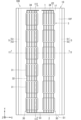
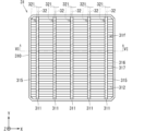
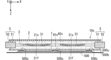
- FIG. 1 is a plan view showing an example of the external appearance of the solar cell module according to the first embodiment when viewed from above.
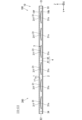
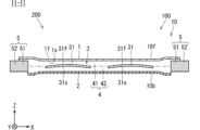
- FIG. 2 is a diagram illustrating an example of a virtual cross section of the solar cell module in FIG. 1 taken along line II-II.
- FIG. 3 is a diagram illustrating an example of a virtual cross section of the solar cell module in FIG. 1 taken along line III-III.
- FIG. 4 is a diagram illustrating an example of the structure of the solar cell element when viewed from above on the first element surface.
- FIG. 5 is a diagram illustrating an example of a structure when the second element surface of the solar cell element is viewed from above.
- FIG. 6 is a diagram illustrating an example of a virtual cross section of the solar cell element of FIGS.
- FIG. 7 is a diagram showing an example of a bent state of the solar cell module according to the first embodiment.
- FIG. 8 is a diagram illustrating an example of a state of a virtual cut surface during manufacturing in a specific example of a method for manufacturing a solar cell element.
- FIG. 9 is a diagram illustrating an example of a state of a virtual cut surface during manufacturing in a specific example of a method for manufacturing a solar cell element.
- FIG. 10 is a diagram illustrating an example of a state of a virtual cut surface during manufacture in a specific example of a method for manufacturing a solar cell element.
- FIG. 11 is a diagram illustrating an example of a state of a virtual cut surface during manufacture in a specific example of a method for manufacturing a solar cell element.
- FIG. 12 is a diagram illustrating an example of a state of a virtual cut surface during manufacturing in a specific example of a method for manufacturing a solar cell element.
- FIG. 13 is a diagram illustrating an example of the state of a virtual cut surface during manufacture in a specific example of the method for manufacturing a solar cell module according to the first embodiment.
- FIG. 14 is a diagram illustrating an example of the state of a virtual cut surface during manufacture in a specific example of the method for manufacturing a solar cell module according to the first embodiment.
- FIG. 12 is a diagram illustrating an example of a state of a virtual cut surface during manufacturing in a specific example of a method for manufacturing a solar cell element.
- FIG. 13 is a diagram illustrating an example of the state of a virtual cut surface during manufacture in a specific example of the method for manufacturing a solar cell module according
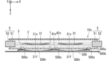
- FIG. 15 is a diagram showing an example of a virtual cut surface at a position corresponding to the virtual cut surface in FIG. 2 of the solar cell module according to the second embodiment.
- FIG. 16 is a diagram illustrating an example of a virtual cut plane at a position corresponding to the virtual cut plane in FIG. 3 of the solar cell module according to the second embodiment.
- FIG. 17 is a diagram illustrating an example of the state of a virtual cut surface during manufacture in a specific example of the method for manufacturing a solar cell module according to the second embodiment.
- FIG. 18 is a diagram illustrating an example of the state of a virtual cut surface during manufacture in a specific example of the method for manufacturing a solar cell module according to the second embodiment.
- FIG. 16 is a diagram illustrating an example of a virtual cut plane at a position corresponding to the virtual cut plane in FIG. 3 of the solar cell module according to the second embodiment.
- FIG. 17 is a diagram illustrating an example of the state of a virtual cut surface during manufacture in a specific example of the method
- FIG. 19 is a plan view showing an example of the external appearance of the solar cell module according to the third embodiment when viewed from above.
- FIG. 20 is a diagram illustrating an example of a virtual cut surface of the solar cell module of FIG. 19 along line XX-XX.
- FIG. 21 is a diagram illustrating an example of a virtual cut surface of the solar cell module of FIG. 19 along line XXI-XXI.
- FIG. 22 is a diagram schematically showing an example of a path through which rainwater flows on the first protective layer of the solar cell module according to the third embodiment.
- FIG. 23 is a diagram illustrating an example of the state of a virtual cut surface during manufacture in a specific example of the method for manufacturing a solar cell module according to the third embodiment.
- FIG. 20 is a diagram illustrating an example of a virtual cut surface of the solar cell module of FIG. 19 along line XX-XX.
- FIG. 21 is a diagram illustrating an example of a virtual cut surface of the solar cell module of FIG
- FIG. 24 is a diagram illustrating an example of the state of a virtual cut surface during manufacture in a specific example of the method for manufacturing a solar cell module according to the third embodiment.
- FIG. 25 is a diagram illustrating an example of a virtual cut plane at a position corresponding to the virtual cut plane in FIG. 20 of the solar cell module according to the fourth embodiment.
- FIG. 26 is a diagram showing an example of a virtual cut surface at a position corresponding to the virtual cut surface in FIG. 21 of the solar cell module according to the fourth embodiment.
- FIG. 27 is a diagram illustrating an example of the state of a virtual cut surface during manufacture in a specific example of the method for manufacturing a solar cell module according to the fourth embodiment.
- FIG. 28 is a diagram illustrating an example of the state of a virtual cut surface during manufacture in a specific example of the method for manufacturing a solar cell module according to the fourth embodiment.
- FIG. 29 is a diagram showing an example of a virtual cut surface at a position corresponding to the virtual cut surface in FIG. 21 of the solar cell module according to another embodiment.
- FIG. 30 is a diagram showing an example of a virtual cut surface at a position corresponding to the virtual cut surface in FIG. 21 of the solar cell module according to another embodiment.
- FIG. 31 is a diagram schematically showing an example of a path through which rainwater flows on the first protective layer of a solar cell module according to another embodiment.
- FIG. 32 is a diagram showing an example of a virtual cut surface at a position corresponding to the virtual cut surface in FIG.
- FIG. 33 is a plan view showing an example of the external appearance of a solar cell module according to another embodiment when viewed from above.
- FIG. 34 is a plan view showing an example of the external appearance of a solar cell module according to another embodiment when viewed from above.
- a solar cell module in which a plurality of solar cell elements are located between a protective layer on the front side and a protective layer on the back side.
- a plurality of solar cell elements are arranged in a plane and electrically connected to each other. Further, the plurality of solar cell elements are covered with a filler containing ethylene vinyl acetate copolymer (EVA) as a main component between the protective layer on the front side and the protective layer on the back side.
- EVA ethylene vinyl acetate copolymer
- FIGS. 1 to 34 A right-handed XYZ coordinate system is shown in FIGS. 1 to 34.
- the longitudinal direction of the front surface 10f of the solar cell panel 10 is set as the ⁇ Y direction as the first direction.
- the lateral direction of the front surface 10f of the solar cell panel 10 is the +X direction as the second direction.
- the direction opposite to the +Z direction is the third direction, which is the -Z direction.
- the direction opposite to the +X direction as the second direction is the -X direction as the fourth direction.
- the direction opposite to the -Y direction as the first direction is the +Y direction as the fifth direction.
- the solar cell module 100 includes, for example, a solar cell panel 10.
- the solar cell panel 10 has, for example, a light-receiving surface (also referred to as a front surface) 10f through which light mainly enters, and a back surface 10b located on the opposite side of the front surface 10f.
- the front surface 10f is in a state facing the +Z direction.
- the back surface 10b is in a state facing the -Z direction.
- the +Z direction is set, for example, in a direction facing the sun, which is in the south.
- the front surface 10f has a rectangular shape.
- Solar cell module 100 may further include a terminal box (not shown) for extracting the power generated by solar cell panel 10 to the outside.
- the solar cell panel 10 includes, for example, a first protective layer 1, a second protective layer 2, a solar cell part 3, a filler 4, and a support member 5.
- a first protective layer 1 As shown in FIGS. 1 to 3, the solar cell panel 10 includes, for example, a first protective layer 1, a second protective layer 2, a solar cell part 3, a filler 4, and a support member 5.
- a second protective layer 2 As shown in FIGS. 1 to 3, the solar cell panel 10 includes, for example, a first protective layer 1, a second protective layer 2, a solar cell part 3, a filler 4, and a support member 5.
- a support member 5 we are prepared.
- the first protective layer 1 has, for example, a first surface 1f and a second surface 1s.
- the first surface 1f constitutes, for example, the front surface 10f of the solar cell panel 10. That is, the first protective layer 1 has a rectangular shape.
- the first surface 1f is exposed to a space (also referred to as external space) 200 outside the solar cell module 100.
- the second surface 1s is a surface of the first protective layer 1 that is opposite to the first surface 1f.
- the first protective layer 1 has, for example, light-transmitting properties. Specifically, the first protective layer 1 has, for example, transparency to light having a wavelength in a specific range.
- the specific range of wavelengths includes, for example, the wavelength of light that can be photoelectrically converted by the solar cell unit 3. If the wavelengths in the specific range include wavelengths of sunlight with high irradiation intensity, the photoelectric conversion efficiency of the solar cell module 100 can be improved.
- the first protective layer 1 As the material of the first protective layer 1, for example, a translucent resin is applied.
- the first protective layer 1 is made of a translucent resin.
- This light-transmitting resin may have weather resistance.
- weather resistance refers to a property that does not easily cause alterations such as deformation, discoloration, and deterioration when used outdoors, for example.
- the light-transmitting resin applied to the material of the first protective layer 1 may have flexibility.
- flexibility means, for example, soft and supple properties.
- the first protective layer 1 may be composed of, for example, one layer of resin.
- the first protective layer 1 has, for example, moisture permeable and waterproof properties.
- Moisture-permeable and waterproof properties for example, reduce the infiltration of water such as water droplets from the external space 200 of the solar cell module 100 toward the solar cell section 3, and also facilitate the passage of moisture from the filler 4 toward the external space 200.
- the resin having translucency and weather resistance includes, for example, a fluorine-based resin.
- Fluorine-based resins include, for example, fluorinated ethylene propylene copolymer (FEP), ethylene tetrafluoroethylene copolymer (ETFE), and ethylene chlorotrifluoroethylene copolymer (Ethylene Chlorotrifluoroethylene). :ECTFE) etc.
- the first protective layer 1 may be composed of two or more layers of resin.
- the fluorine-based resin applied to the first protective layer 1 may be, for example, two or more types of resin. Therefore, for example, a mode is conceivable in which the fluororesin applied to the first protective layer 1 includes one or more resins among FEP, ETFE, and ECTFE.
- the thickness of the first protective layer 1 is, for example, about 0.05 millimeter (mm) to 0.5 mm.
- the first protective layer 1 may be made of a moisture-permeable resin with a relatively low density. Moreover, the thickness of the first protective layer 1 may be thin. In this case, the first protective layer 1 is light. Therefore, the solar cell module 100 can be made lighter and thinner than, for example, a structure in which a high-density glass having a thickness of about 1 mm or more is used instead of the first protective layer 1.
- the material of the first protective layer 1 a resin different from the fluorine-based resin may be used instead of the fluorine-based resin, or together with the fluorine-based resin.
- a resin different from the fluorine-based resin for example, acrylic resin or polycarbonate is used as the resin different from the fluorine-based resin.
- the thickness of the resin is, for example, about 0.03 mm to 0.6 mm.
- the first protective layer 1 may have a structure in which a plurality of types of resins are laminated.
- the solar cell section 3 is located, for example, between the first protective layer 1 and the second protective layer 2. In other words, the solar cell section 3 is in a state of facing the first protective layer 1 and also facing the second protective layer 2 in the Z direction.
- the solar cell section 3 includes, for example, a plurality of solar cell elements 31.
- the plurality of solar cell elements 31 are located between the second surface 1s of the first protective layer 1 and the second protective layer 2. From another perspective, the plurality of solar cell elements 31 are located facing the second surface 1s of the first protective layer 1. Moreover, the plurality of solar cell elements 31 are lined up along the second surface 1s of the first protective layer 1. In other words, the plurality of solar cell elements 31 are arranged in a plane along the second surface 1s of the first protective layer 1. In the examples shown in FIGS. 1 to 3, the plurality of solar cell elements 31 are two-dimensionally lined up.
- the solar cell section 3 further includes, for example, a plurality of first wiring members 32, a second wiring member 33, and a third wiring member 34.
- the solar cell section 3 includes, for example, a plurality of solar cell strings 30.
- the solar cell section 3 includes two solar cell strings 30 as the plurality of solar cell strings 30.
- the plurality of solar cell strings 30 are lined up in the X direction.
- Each of the plurality of solar cell strings 30 includes, for example, two or more solar cell elements 31 and a plurality of first wiring members 32.
- each solar cell string 30 in each solar cell string 30, two or more solar cell elements 31 are lined up in, for example, the ⁇ Y direction as the first direction.
- each solar cell string 30 includes six solar cell elements 31 as the two or more solar cell elements 31.
- each solar cell string 30 may include two solar cell elements 31 as the two or more solar cell elements 31, or may include an arbitrary number of three or more solar cell elements 31. good.
- the plurality of solar cell elements 31 include two solar cell elements 31 lined up in the ⁇ Y direction as the first direction.
- the plurality of first wiring members 32 are in a state of electrically connecting two mutually adjacent solar cell elements 31 among the two or more solar cell elements 31.
- the second wiring member 33 is in a state of electrically connecting two adjacent solar cell strings 30 of the two or more solar cell strings 30 .
- One third wiring member 34 is connected to each of the two solar cell strings 30.
- the solar cell section 3 is connected to the third wiring member 34 connected to the solar cell string 30 located at the end in the -X direction and the third wiring member 34 located at the end in the +X direction. and a third wiring member 34 connected to the solar cell string 30 that is connected to the solar cell string 30.
- Each of the two third wiring members 34 has a portion drawn out to the outside of the solar cell panel 10.
- Each of the plurality of solar cell elements 31 can convert light energy into electrical energy.
- Each of the plurality of solar cell elements 31 has, for example, a plate-like shape.
- Each of the plurality of solar cell elements 31 has a first element surface 31f and a second element surface 31s.
- the first element surface 31f is a surface facing the second surface 1s of the first protective layer 1.
- the second element surface 31s is a surface of the solar cell element 31 on the opposite side to the first element surface 31f. In other words, the second element surface 31s faces the second protective layer 2.
- the first element surface 31f is in a state facing the +Z direction
- the second element surface 31s is in a state facing the ⁇ Z direction.
- the first element surface 31f primarily serves as a surface on which light is incident (also referred to as a light-receiving surface), and the second element surface 31s primarily serves as a surface on which light is not incident (non-light-receiving surface). It has a role as a surface (also called a surface).
- Each of the first element surface 31f and the second element surface 31s has a rectangular shape such as a substantially square shape, for example.
- Each of the first element surface 31f and the second element surface 31s may have a shape in which corners are cut.
- Each of the first element surface 31f and the second element surface 31s has, for example, a substantially square shape with a side length of about 100 mm to 250 mm.
- Each of the first element surface 31f and the second element surface 31s may have a substantially rectangular shape, for example.
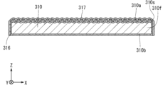
- each of the plurality of solar cell elements 31 includes a semiconductor substrate 310, a first electrode 311, a second electrode 312, a third electrode 313, a fourth electrode 314.
- the semiconductor substrate 310 includes, for example, a crystalline semiconductor such as crystalline silicon, an amorphous semiconductor such as amorphous silicon, four types of elements such as copper, indium, gallium, and selenium, or two types of elements such as cadmium and tellurium. Compound semiconductors using Here, it is assumed that crystalline silicon is applied to the semiconductor substrate 310.
- the semiconductor substrate 310 mainly includes a semiconductor region 310f having a first conductivity type (also referred to as a first conductivity type region) and a second conductivity type region 310f opposite to the first conductivity type. It has a semiconductor region (also referred to as a second conductivity type region) 310s having a conductivity type.
- the first conductivity type region 310f is located, for example, on the second element surface 31s side of the semiconductor substrate 310 in the ⁇ Z direction.
- the second conductivity type region 310s is located, for example, in a surface layer portion of the semiconductor substrate 310 on the first element surface 31f side in the +Z direction.
- the semiconductor substrate 310 has a pn junction located at the interface between the first conductivity type region 310f and the second conductivity type region 310s.
- the thickness of the semiconductor substrate 310 is, for example, about 0.15 mm to 0.5 mm.
- each solar cell element 31 has a plurality of first electrodes 311 and a plurality of second electrodes 312.
- a plurality of substantially parallel first electrodes 311 and a large number of substantially parallel second electrodes 312 are located on the first element surface 31f side of the semiconductor substrate 310.
- first electrodes 311 as a plurality of substantially parallel first electrodes 311 and a large number of second electrodes 312 as a plurality of substantially parallel second electrodes 312 are substantially perpendicular to each other. It is located in a state of being.
- each of the plurality of first electrodes 311 has a long shape elongated in the -Y direction as the first direction
- each of the plurality of second electrodes 312 has a long shape in the -Y direction as the first direction. It has a linear shape that is long in the +X direction.
- each solar cell element 31 has a fifth electrode 315 located along the outer edge in the -X direction and a fifth electrode 315 located along the outer edge in the +X direction on the first element surface 31f side, for example. and a fifth electrode 315 located along the line.
- Each fifth electrode 315 interconnects, for example, a large number of substantially parallel second electrodes 312 .
- an antireflection film 317 may be located on the second conductivity type region 310s of the semiconductor substrate 310 in a region where the first electrode 311 and the second electrode 312 are not formed.
- an insulating film made of silicon nitride or the like is applied to the antireflection film 317.
- a passivation film 316 may be present between the second conductivity type region 310s of the semiconductor substrate 310 and the antireflection film 317.
- a thin film made of an oxide such as aluminum oxide or a nitride is applied to the passivation film 316.
- the main component of the first electrode 311 when the main component of the first electrode 311 is silver, the silver paste is applied in a desired shape by a screen printing method or the like, and then the silver paste is fired, thereby forming the first electrode 311. 311 may be formed.
- the term "main component” refers to a component that has the largest (highest) ratio (also referred to as content rate) of the components constituting a substance.
- a metal paste containing a metal powder containing silver as a main component, an organic vehicle, and a glass frit is applied to the silver paste.
- the main component of the second electrode 312 when the main component of the second electrode 312 is silver, the second electrode 312 is formed by applying a silver paste into a desired shape using a screen printing method or the like and then firing the silver paste.
- the fifth electrode 315 is formed by applying a silver paste into a desired shape using a screen printing method or the like, and then firing the silver paste. can be done.
- the first electrode 311, the second electrode 312, and the fifth electrode 315 may be formed in separate steps, or may be formed in the same step.
- the third electrode 313 and the fourth electrode 314 are located on the second element surface 31s side of the semiconductor substrate 310, for example.
- a busbar electrode is applied to the third electrode 313.
- a plurality of substantially parallel third electrodes 313 are located on the second element surface 31s side of the semiconductor substrate 310. More specifically, five rows of third electrodes 313 that are substantially parallel to each other are located on the second element surface 31s side of the semiconductor substrate 310.
- Each of the five rows of third electrodes 313 is located along the -Y direction, which is the first direction. More specifically, each of the five rows of third electrodes 313 includes, for example, a plurality of electrode parts lined up in a row.
- the plurality of electrode parts is composed of, for example, six electrode parts.
- the fourth electrode 314 is located on the second element surface 31s side of the semiconductor substrate 310, except for a portion where the third electrode 313 and the fourth electrode 314 overlap and are connected to each other. It is located on almost the entire surface of the area where it is not located. Note that the fourth electrode 314 does not need to be located on substantially the entire surface, and may be located in a grid pattern, for example.
- a passivation film 316 may be present between the first conductivity type region 310f of the semiconductor substrate 310 and the third electrode 313 and the fourth electrode 314. .
- a thin film made of an oxide such as aluminum oxide or a nitride is applied to the passivation film 316.
- the passivation film 316 has a desired pattern between the first conductivity type region 310f and the third electrode 313 and the fourth electrode 314.
- a film (also referred to as a protective film) 318 for protecting the passivation film 316 may be present between the passivation film 316 and the fourth electrode 314.
- the protective film 318 For example, a thin film made of an oxide such as silicon oxide is used as the protective film 318.
- the protective film 318 has a desired pattern between the passivation film 316 and the fourth electrode 314.
- the protective film 318 does not need to be present between the passivation film 316 and the third electrode 313 as shown in FIG.
- the protective film 318 has a plurality of holes in which the third electrode 313 is located.
- the protective film 318 may be present between the passivation film 316 and the third electrode 313.
- the passivation film 316 and the protective film 318 have, for example, a large number of through holes for bringing a part of the fourth electrode 314 into contact with the first conductivity type region 310f.
- the first conductivity type region 310f is a region in which the concentration of a dopant element of the first conductivity type is higher than other regions of the first conductivity type region 310f (also referred to as a high concentration region) in a portion of the surface layer that is in contact with the fourth electrode 314. It has a BSF (Back Surface Field) area) of 310t.
- the main component of the third electrode 313 is silver
- the silver paste is applied in a desired shape by a screen printing method or the like, and then the silver paste is fired, thereby forming the third electrode 313.
- 313 may be formed.
- the main component of the fourth electrode 314 is aluminum
- the fourth electrode 314 is formed by applying aluminum paste into a desired shape using a screen printing method or the like, and then firing the aluminum paste. can be done.
- a metal paste containing a metal powder containing aluminum as a main component, an organic vehicle, and a glass frit is applied to the aluminum paste.
- the first wiring material 32 electrically connects, for example, the first electrode 311 of one solar cell element 31 and the third electrode 313 of another solar cell element 31 adjacent to this one solar cell element 31. It is in a connected state.
- the outer edges of the plurality of first wiring members 32 attached to each of the solar cell elements 31 are virtually drawn with thin two-dot chain lines.
- the first wiring member 32 has an elongated shape that is elongated in the ⁇ Y direction as the first direction.
- the first wiring material 32 is in a state of being joined to the first electrode 311 and the third electrode 313, for example.
- first wiring material 32 and the first electrode 311 there is a part (also referred to as a first joint part) 321 where the first wiring material 32 and the first electrode 311 are joined. exists. Therefore, for example, the first wiring material 32 is in a state of being bonded to the first electrode 311 of one solar cell element 31 via the first bonding portion 321. Further, for example, between the first wiring material 32 and the third electrode 313, there is a part 322 that joins the first wiring material 32 and the third electrode 313 (also referred to as a second joint part). There is. Therefore, for example, the first wiring material 32 is in a state of being joined to the third electrode 313 of another solar cell element 31 adjacent to one solar cell element 31 via the second joint portion 322. .
- the material for the first joint portion 321 and the second joint portion 322 may be, for example, a low melting point alloy such as solder or a low melting point single metal. More specifically, for example, a copper foil having a thickness of about 0.1 mm to 0.2 mm and a width of about 1 mm to 2 mm is applied to the first wiring material 32. In this case, the entire surface of the first wiring material 32 may be coated with solder.
- the first wiring material 32 is in a state of being electrically connected to the first electrode 311 and the third electrode 313, for example, by soldering.
- the solder located between the first wiring material 32 and the first electrode 311 constitutes the first joint portion 321.
- the solder located between the first wiring material 32 and the third electrode 313 constitutes the second joint portion 322 .
- the filler 4 is in contact with the second surface 1s. Further, the filler 4 is positioned so as to cover the plurality of solar cell elements 31. In the first embodiment, the filler 4 is in a state covering the plurality of solar cell elements 31 between the first protective layer 1 and the second protective layer 2. In other words, the filler 4 covers the solar cell part 3 in the area between the first protective layer 1 and the second protective layer 2 (also referred to as the gap area), and is filled in this gap area. It is in. From another perspective, the filler 4 has a surface on the first protective layer 1 side that is in contact with the second surface 1s of the first protective layer 1 and a surface that is in contact with the second protective layer 2. It has a certain second protective layer 2 side surface.
- the filler 4 includes, for example, a filler (also referred to as a first filler) 41 located on the front surface 10f side and a filler (also referred to as a second filler) 42 located on the back surface 10b side.
- a filler 41 is in a state of covering the entire surface of the solar cell section 3 on the first protective layer 1 side.
- the first filler 41 is in a state of covering the plurality of solar cell elements 31, for example, between the first protective layer 1 and the plurality of solar cell elements 31.
- the second filler 42 is in a state, for example, covering the entire surface of the solar cell section 3 on the second protective layer 2 side.
- the second filler 42 is in a state of covering the plurality of solar cell elements 31, for example, between the second protective layer 2 and the plurality of solar cell elements 31. Therefore, in the first embodiment, the solar cell section 3 is sandwiched and surrounded by, for example, the first filler 41 and the second filler 42 . Thereby, for example, the attitude of the solar cell section 3 can be maintained by the filler 4.
- the filler 4 has, for example, translucency.
- the filler 4 has, for example, translucency to light having a wavelength in the above-mentioned specific range. For example, if at least the first filler 41 out of the first filler 41 and the second filler 42 constituting the filler 4 has translucency, the incident light from the front surface 10f side It can reach up to the solar cell section 3.
- the material of the first filler 41 for example, polyvinyl acetal such as ethylene-vinyl acetate copolymer (EVA), polyvinyl butyral (PVB), or acid-modified resin is used.
- EVA ethylene-vinyl acetate copolymer
- PVB polyvinyl butyral
- acid-modified resin includes, for example, a modified polyolefin resin that can be formed by graft modification of a resin such as polyolefin with an acid.
- acids that can be used for graft modification of acid-modified resins include acrylic acid, methacrylic acid, maleic acid, fumaric acid, itaconic acid, maleic anhydride, hymic anhydride, itaconic anhydride, and citraconic anhydride.
- Ru As the material for the second filler 42, for example, like the first filler 41, polyvinyl acetal such as EVA and PVB, acid-modified resin, etc. are used.
- Each of the first filler 41 and the second filler 42 may be made of two or more types of materials, for example.
- the second filler 42 may contain, for example, a pigment.
- a pigment for example, if the second filler 42 contains a white pigment, the light that has passed through the solar cell section 3 can be reflected by the second filler 42 and made to enter the solar cell section 3 again. . Thereby, the power generation efficiency of the solar cell module 100 can be improved.
- the filler 4 may not include the second filler 42 but may include the first filler 41.
- the first filler 41 is in a state covering the solar cell section 3 between the first protective layer 1 and the second protective layer 2.
- the first filler 41 is in a state covering the plurality of solar cell elements 31 between the first protective layer 1 and the second protective layer 2.
- the thickness of the filler 4 may be smaller in the portion covering the solar cell portion 3 and greater in the portion between the solar cell portion 3 and the support member 5.
- the maximum value of the thickness of the filler 4 between the solar cell section 3 and the support member 5 is the same as that between two adjacent solar cell elements 31 among the plurality of solar cell elements 31. It is larger than the maximum thickness of the filler 4.
- the distance between the first protective layer 1 and the second protective layer 2 is small in the area where the solar cell part 3 is sandwiched, and the distance between the first protective layer 1 and the second protective layer 2 is small in the area where the solar cell part 3 and the support member 5 are sandwiched. It may be large in the part where it is.
- the maximum value of the distance between the first protective layer 1 and the second protective layer 2 in the area sandwiching the area between the solar cell part 3 and the support member 5 is the part where the solar cell part 3 is sandwiched. It may be larger than the maximum value of the distance between the first protective layer 1 and the second protective layer 2 in .
- the thickness of the filler 4 increases as it goes from the solar cell section 3 toward the support member 5. Gradually increasing portions may also be present. In other words, for example, in at least a part of the region between the support member 5 and the solar cell section 3, the thickness of the filler 4 monotonically increases from the solar cell section 3 toward the support member 5. may exist.
- the filler 4 has a shape that is line symmetrical to each other with respect to the XY plane, but the drawing is only schematically shown and is not necessarily limited to this.
- the second protective layer 2 is in a state of forming the back surface 10b of the solar cell panel 10, for example.
- the second protective layer 2 is in contact with, for example, the surface of the filler 4 on the side opposite to the first protective layer 1 .
- the second protective layer 2 is in contact with the filler 4 on the opposite side of the filler 4 from the first protective layer 1 .
- the second protective layer 2 is in contact with the filler 4 at a surface of the filler 4 that is opposite to the surface of the filler 4 that is in contact with the first protective layer 1 .
- the second protective layer 2 is located facing the solar cell section 3 and the first portion 51 of the support member 5 in the Z direction.
- the first portion 51 is a portion of the support member 5 that is located closer to the solar cell unit 3 than the second portion 52 in the X direction.
- the second protective layer 2 can, for example, protect the solar cell section 3 from the back surface 10b side.
- a back sheet forming the back surface 10b is applied to the second protective layer 2.
- the thickness of the back sheet is, for example, about 0.15 mm to 0.5 mm.
- resin is used as the material for the back sheet.
- the same material as the first protective layer 1 can be applied to this resin.
- the second protective layer 2 has the same or substantially the same shape as the first protective layer 1 when viewed from the rear surface 10b side. For example, a configuration is adopted in which both the first protective layer 1 and the second protective layer 2 have a rectangular outer shape when viewed from the rear surface 10b side.
- the support member 5 is a member for improving the rigidity of the solar cell panel 10.
- the support member 5 has higher rigidity than all of the first protective layer 1, second protective layer 2, and filler 4.
- the support member 5 is, for example, a rigid body having high rigidity.
- metal may be used as the material of the support member 5. This metal may be, for example, aluminum or stainless steel.
- the support member 5 is located adjacent to the solar cell section 3 with a space therebetween. More specifically, the support member 5 is located adjacent to the solar cell section 3 with a space therebetween in a plan view.
- Support member 5 includes a first portion 51 and a second portion 52.
- Planar view means a planar view of each part as viewed in the ⁇ Z direction as the third direction, unless specific conditions are stated. From another point of view, when viewed from above toward the first surface 1f of the first protective layer 1, the support member 5 is adjacent to the solar cell section 3 with an interval in the +X direction as the second direction. It is located in a state of being.
- the first portion 51 is located between the first protective layer 1 and the second protective layer 2 and covered with the filler 4. In other words, the first portion 51 is located facing the second surface 1s of the first protective layer 1. Further, the first portion 51 is located facing the second protective layer 2 . In the example of FIG. 2, the first portion 51 is in a state facing the second surface 1s of the first protective layer 1 in the Z direction. The first portion 51 also faces the second protective layer 2 in the Z direction.
- the filler 4 includes a portion located between the second surface 1s of the first protective layer 1 and the first portion 51. More specifically, the first filler 41 includes a portion located between the second surface 1s of the first protective layer 1 and the first portion 51 in the ⁇ Z direction as the third direction. Further, the filler 4 includes a portion located between the second protective layer 2 and the first portion 51. More specifically, the second filler 42 includes a portion located between the first portion 51 and the second protective layer 2 in the -Z direction as the third direction.
- the second portion 52 is a portion of the support member 5 located on the opposite side to the solar cell section 3 side.
- the support member 5 includes a first portion 51 located on the solar cell section 3 side, and a second portion 52 located on the opposite side of the solar cell section 3 with respect to the first section 51. ,including.
- the second portion 52 may be considered to be a portion of the support member 5 other than the first portion 51 .
- the second portion 52 is in a state of protruding from the first portion 51 from the filler 4 covering the first portion 51 in a direction opposite to the solar cell portion 3 . More specifically, the second portion 52 is located on the opposite side (also referred to as the outside) of the solar cell section 3 with respect to the first portion 51 in plan view.
- the second portion 52 is located not facing the second surface 1s of the first protective layer 1, and is not covered with the filler 4.
- the second portion 52 is in a state of protruding from the first portion 51 to the outside of the first protective layer 1 and the second protective layer 2 in plan view.
- the second portion 52 is not facing the first protective layer 1 in the Z direction.
- the second portion 52 is in a state where it does not also face the second protective layer 2 in the Z direction.
- the first portion 51 is located on the solar cell section 3 side (also referred to as inside) with respect to the second portion 52 in plan view.
- the support member 5 has a plate-like shape. More specifically, the support member 5 has a rectangular shape in plan view. In the example of FIG. 2, the XZ cross section of the support member 5 also has a rectangular shape. The corners of the support member 5 may be chamfered as appropriate.
- the longitudinal direction of the support member 5 is located along one side of the first protective layer 1, for example.
- the longitudinal direction of the support member 5 is the Y direction.
- the longitudinal direction of the support member 5 is located, for example, along the direction in which two or more solar cell elements 31 are arranged in one solar cell string 30 (also referred to as the arrangement direction).
- the arrangement direction of the plurality of solar cell elements 31 in one solar cell string 30 is the Y direction.
- the longitudinal direction of the support member 5 is located along the longitudinal direction of the first wiring member 32, for example.
- the longitudinal direction of the first wiring member 32 is the Y direction.
- the solar cell panel 10 includes two support members 5.
- the two support members 5 include a first support member 5 and a second support member 5.
- the first support member 5 is located at the end of the solar cell panel 10 in the ⁇ X direction, which is the fourth direction.
- the second support member 5 is located at the end of the solar cell panel 10 in the +X direction as the second direction.
- the second portion 52 is located on the side of the first portion 51 in the ⁇ X direction, which is the fourth direction.
- the second portion 52 is located on the side of the first portion 51 in the +X direction as the second direction.
- the first support member 5 is located along the first side of the first protective layer 1.
- the first side is one side of the first protective layer 1 located at the end in the ⁇ X direction as the fourth direction.
- the second support member 5 is located along the second side of the first protective layer 1 .
- the second side is one side of the first protective layer 1 located at the end in the +X direction as the second direction.
- each of the first side and the second side is located extending along the Y direction.
- Each of the two support members 5 has a rectangular front and back surface whose longitudinal direction is the Y direction and whose transversal direction is the X direction.
- the length of each support member 5 in the longitudinal direction is, for example, the same or approximately the same as the length of the first protective layer 1.
- each support member 5 in the lateral direction is set to, for example, several tens of mm or more.
- the length (width) of the first portion 51 in the transverse direction is set to, for example, about 20% to 80% of the width of the support member 5.
- the thickness of each support member 5 is larger than the thickness of the solar cell section 3, for example.
- the thickness of each support member 5 is set, for example, to about 1 mm to 5 mm.
- the second portion 52 of the support member 5 is attached, for example, to a portion to which a building material or the like is to be attached (also referred to as an attachment target portion).
- the second portion 52 may have a mounting hole (not shown).
- This attachment hole is a hole (also referred to as a through hole) that penetrates the second portion 52 in the Z direction.
- a mounting part also referred to as a mounting part
- the solar panel 10 can be attached to the attachment target part.
- the support members 5 are located at each end of the solar cell panel 10 in the -X direction as the fourth direction and the end in the +X direction as the second direction. Therefore, the two support members 5 located at both ends of the solar cell panel 10 in the X direction can be fixed to the attachment target part. Thereby, the solar cell panel 10 can be firmly attached to the attachment target part. Therefore, the support member 5 has a role as a member (also referred to as an attachment member) for attaching the solar cell panel 10 to an object to be attached. Therefore, by providing the support member 5, the solar cell module 100 can easily and stably fix the solar cell module 100 to the attachment target part.
- the support members 5 are not mainly located on both sides of the solar cell panel 10 in the Y direction. More specifically, the support member 5 supports each of the -Y direction end (also referred to as a first end) E1 and the +Y direction end (also referred to as a second end) E2 of the solar cell panel 10. is not actually located.
- the first end E1 and the second end E2 are ends along the X direction. Therefore, as shown in FIG. 7, by applying the external force F1 to the support member 5, the solar cell panel 10 can be bent in an arc shape when viewed in the direction along the +Y direction.
- the solar cell panel 10 can bend to a state along an arc with a radius of about several hundred mm.
- a case can be considered in which a circular arc of approximately several hundred mm is a circular arc of approximately 500 mm. Thereby, the solar cell panel 10 can be easily attached to the curved attachment target part.
- a configuration is adopted in which one of the YZ cross section and the XZ cross section of the solar cell element 31 is curved in a convex shape protruding toward the second surface 1s.
- the YZ cross section of the solar cell element 31 is a virtual cross section along each of the -Y direction as the first direction and the -Z direction as the third direction of the solar cell element 31.
- the XZ cross section of the solar cell element 31 is a virtual cross section along each of the +X direction as the second direction and the -Z direction as the third direction of the solar cell element 31.
- the XZ cross section of the first element surface 31f is curved in a convex shape protruding toward the second surface 1s, and the XZ cross section of the second element surface 31s is curved toward the second surface 1s.
- a curved shape that is concave in the direction toward the surface 1s is adopted.
- the XZ cross section of the first element surface 31f is a virtual cross section along the +X direction as the second direction and the ⁇ Z direction as the third direction with respect to the first element surface 31f.
- the XZ cross section of the second element surface 31s is a virtual cross section along the +X direction as the second direction and the ⁇ Z direction as the third direction with respect to the second element surface 31s.
- the first element surface 31f is curved in a convex shape along the first virtual arc surface.
- the first virtual arc surface is a circular arc that is curved in a convex shape protruding toward the +Z direction, which is opposite to the -Z direction as the third direction, in the -Y direction as the first direction on the XZ plane. It is a virtual curved surface formed by The XZ plane is a virtual plane along the +X direction as the second direction and the -Z direction as the third direction.
- the second element surface 31s is curved concavely along the second virtual arc surface.
- the second virtual arc surface is a circular arc that is curved in a convex shape protruding toward the +Z direction, which is opposite to the -Z direction as the third direction, in the -Y direction as the first direction on the XZ plane. It is a virtual curved surface formed by For example, the second virtual arc surface is located along the first virtual arc surface.
- the YZ cross section of the first element surface 31f is curved in a convex shape protruding toward the second surface 1s
- the YZ cross section of the second element surface 31s is curved toward the second surface 1s.
- a curved shape that is concave in the direction toward the surface 1s may be adopted.
- the first element surface 31f is curved in a convex shape along the third virtual arc surface.
- the third virtual arc surface is a circular arc that is curved in a convex shape protruding toward the +Z direction, which is opposite to the -Z direction as the third direction, in the YZ plane, and extends in the +X direction as the second direction.
- the YZ plane is a virtual plane along each of the -Y direction as the first direction and the -Z direction as the third direction.
- the second element surface 31s is curved concavely along the fourth virtual arc surface.
- the fourth virtual arc surface is a circular arc that is curved in a convex shape protruding toward the +Z direction, which is opposite to the -Z direction as the third direction, in the +X direction as the second direction on the YZ plane. It is a virtual curved surface formed by For example, the fourth virtual arc surface is located along the third virtual arc surface.
- the solar cell element 31 may be curved along a virtual spherical surface.
- the first element surface 31f may have a convexly curved shape along a part of the first virtual spherical surface
- the second element surface 31s may have a shape that is curved in a convex manner along a part of the first virtual spherical surface. , it may have a shape that is concavely curved along a part of the second virtual spherical surface.
- the second virtual spherical surface is located along the first virtual spherical surface.
- the radius of each of the first virtual spherical surface and the second virtual spherical surface is set, for example, to approximately several hundred mm to several thousand mm.
- the first protective layer 1 is made of a transparent resin. Therefore, for example, by making the first protective layer 1 thinner, the weight of the solar cell module 100 can be reduced.
- the first element surface 31f facing the second surface 1s of the first protective layer 1 has a convex shape. It is curved to. Further, for example, in each of the plurality of solar cell elements 31 of the solar cell section 3, the second element surface 31s on the opposite side to the first element surface 31f is curved in a concave shape. From another point of view, the plate-shaped solar cell element 31 has a curved convex shape protruding toward the second surface 1s of the first protective layer 1.
- the solar cell element 31 is curved in a convex shape protruding toward the first protective layer 1, various objects such as falling objects and flying objects collide with the first protective layer 1.
- the impact on the solar cell element 31 can be alleviated.
- the solar cell element 31 becomes difficult to break.
- the impact resistance of the solar cell element 31 can be improved.
- the power generation efficiency of the solar cell module 100 is less likely to decrease. Therefore, for example, it is possible to achieve both weight reduction and improvement in power generation efficiency in the solar cell module 100. That is, it is possible to reduce the weight of the solar cell module 100 and improve the power generation efficiency.
- the solar cell element 31 is curved in a convex shape protruding toward the first protective layer 1, the impact resistance of the solar cell element 31 can be improved. Therefore, by making the first protective layer 1 thinner, it is possible to reduce the weight of the solar cell module 100. As a result, for example, it is possible to achieve both weight reduction and improvement in power generation efficiency in the solar cell module 100.
- a semiconductor substrate 310 is prepared.
- Semiconductor substrate 310 has a first surface 310a and a second surface 310b opposite to first surface 310a.
- the semiconductor substrate 310 may be formed using, for example, the existing Czochralski (CZ) method or casting method.
- CZ Czochralski
- an example using an ingot of p-type polycrystalline silicon as the first conductivity type produced by a casting method will be described.
- the semiconductor substrate 310 is manufactured by slicing this ingot to a desired thickness of, for example, 250 ⁇ m or less.
- etching the surface of the semiconductor substrate 310 in a small amount with an aqueous solution such as sodium hydroxide, potassium hydroxide, or fluoronitric acid
- an aqueous solution such as sodium hydroxide, potassium hydroxide, or fluoronitric acid
- Textured structures can be formed by wet or dry etching.
- Wet etching may be performed using, for example, an alkaline aqueous solution such as sodium hydroxide or an acidic aqueous solution such as fluoronitric acid.
- Dry etching may be performed using, for example, a reactive ion etching (RIE) method.
- RIE reactive ion etching
- a second conductivity type region 310s which is an n-type semiconductor region as a second conductivity type, is formed on a first surface 310a of the semiconductor substrate 310 having a textured structure. More specifically, a second conductivity type region 310s, which is a region of an n-type semiconductor as a second conductivity type, is formed in a surface layer portion of the semiconductor substrate 310 on the first surface 310a side having a textured structure.
- the second conductivity type region 310s may be formed using, for example, a coating thermal diffusion method or a vapor phase thermal diffusion method.
- the coating thermal diffusion method includes, for example, applying diphosphorus pentoxide (P 2 O 5 ) in the form of a paste onto the surface of the semiconductor substrate 310 to thermally diffuse phosphorus.
- the vapor phase thermal diffusion method uses, for example, gaseous phosphorus oxychloride (POCl 3 ) as a diffusion source.
- POCl 3 gaseous phosphorus oxychloride
- the second conductivity type region 310s formed on the second surface 310b side is treated with an aqueous solution of fluoronitric acid. Remove by etching.
- the phosphorus glass attached to the first surface 310a side of the semiconductor substrate 310 when forming the second conductivity type region 310s is removed by etching.
- a diffusion mask may be formed in advance on the second surface 310b side of the semiconductor substrate 310, the second conductivity type region 310s may be formed by a vapor phase thermal diffusion method, and then the diffusion mask may be removed. good.
- a passivation film 316 is formed at least on the second surface 310b of the semiconductor substrate 310.
- a passivation film 316 is formed on each of the second surface 310b and the first surface 310a of the semiconductor substrate 310.
- the passivation film 316 may be composed of, for example, a film mainly containing aluminum oxide.
- the passivation film 316 may be formed by, for example, an atomic layer deposition (ALD) method.
- ALD atomic layer deposition
- the passivation film 316 can be formed all around the semiconductor substrate 310 including the end surface.
- the step of forming the passivation film 316 by the ALD method first, the semiconductor substrate 310, on which the second conductivity type region 310s has been formed, is placed in a chamber of a film forming apparatus. Then, the following steps A to D are repeated multiple times while the semiconductor substrate 310 is heated to a temperature range of about 100 degrees Celsius (100 degrees Celsius) to 250 degrees Celsius (250 degrees Celsius), thereby removing aluminum oxide mainly.
- a passivation film 316 containing As a result, a passivation film 316 having a desired thickness is formed.
- Step A An aluminum raw material such as trimethylaluminum (TMA) for forming aluminum oxide is supplied onto the semiconductor substrate 310 together with a carrier gas such as Ar gas or nitrogen gas. As a result, the aluminum raw material is adsorbed all around the semiconductor substrate 310.
- the time for which TMA is supplied is set, for example, to about 15 milliseconds to 3000 milliseconds.
- the surface of the semiconductor substrate 310 is terminated with hydroxyl groups (OH groups).
- the surface of the semiconductor substrate 310 has a Si--O--H structure. This structure can be formed, for example, by treating the semiconductor substrate 310 with dilute hydrofluoric acid and cleaning with pure water in the order described.
- Step B The inside of the chamber of the film forming apparatus is cleaned using nitrogen gas.
- the aluminum raw material in the chamber is removed, and the aluminum raw materials other than the component chemically adsorbed at the atomic layer level among the aluminum raw materials physically adsorbed and chemically adsorbed on the semiconductor substrate 310 are removed.
- the time for purifying the inside of the chamber with nitrogen gas is set, for example, from about 1 second to several tens of seconds.
- Step C An oxidizing agent such as water or ozone gas is supplied into the chamber of the film forming apparatus. As a result, the alkyl group contained in TMA is removed and replaced with an OH group. As a result, an atomic layer of aluminum oxide is formed on the semiconductor substrate 310.
- the time for supplying the oxidizing agent into the chamber is set, for example, to about 750 milliseconds to 1100 milliseconds.
- hydrogen may be supplied into the chamber together with an oxidizing agent to cause the aluminum oxide to contain hydrogen atoms.
- Step D Purify the chamber of the film forming apparatus with nitrogen gas. This removes the oxidizing agent in the chamber.
- the oxidizing agent that did not contribute to the reaction during the formation of aluminum oxide at the atomic layer level on the semiconductor substrate 310 is removed.
- the time for purifying the inside of the chamber with nitrogen gas is set, for example, from about 1 second to several tens of seconds.
- an antireflection film 317 is formed on the passivation film 316.
- the antireflection film 317 may be made of, for example, a silicon nitride film.
- the antireflection film 317 may be formed using, for example, a plasma-enhanced chemical vapor deposition (PECVD) method or a sputtering method.
- PECVD plasma-enhanced chemical vapor deposition
- the semiconductor substrate 310 is heated in advance to a temperature higher than the temperature during the formation of the antireflection film 317.
- the reaction pressure is set to about 50 Pascals (Pa) to 200 Pa, and a mixed gas of silane and ammonia diluted with nitrogen gas is turned into plasma by glow discharge decomposition and deposited on the heated semiconductor substrate 310. let As a result, an antireflection film 317 is formed on the semiconductor substrate 310.
- the film-forming temperature is set to about 350° C.
- the pre-heating temperature of the semiconductor substrate 310 is set to be about 50° C. higher than the film-forming temperature.
- a frequency of approximately 10 kilohertz (kHz) to 500 kHz is adopted.
- the flow rate of the gas is appropriately determined depending on the size of the reaction chamber and the like.
- the gas flow rate is set in a range of about 150 ml/min to 6000 ml/min.
- the value (B/A) obtained by dividing the flow rate B of ammonia gas by the flow rate A of silane gas is set in a range of 0.5 to 1.5.
- a protective film 318 having a desired pattern is formed on the passivation film 316 at least on the second surface 310b side of the semiconductor substrate 310.
- the desired pattern includes a large number of through holes and the like.
- the protective film 318 can be formed, for example, by a wet or dry process. For example, a process using solution application is applied to the wet process. For example, a process using PECVD or sputtering is applied to the dry process.
- a protective film 318 is formed by drying this solution.
- the desired pattern includes a large number of through holes.
- an insulating paste is used as the solution.
- an insulating paste for example, an insulating paste containing a siloxane resin that is a raw material for the protective film 318, an organic solvent, and a plurality of fillers is used.
- a siloxane resin is a siloxane compound having a siloxane bond (Si--O--Si bond).
- siloxane resin a low molecular weight resin having a molecular weight of 15,000 or less, which is produced by hydrolyzing alkoxysilane or silazane and subjecting the resin to condensation polymerization, is used.
- Application of the solution can be performed using, for example, a screen printing method. Drying of the solution after application can be performed using, for example, a hot plate or a drying oven.
- electrodes including a first electrode 311, a second electrode 312, a third electrode 313, and a fourth electrode 314 are formed.
- a material for forming the first electrode 311 and the second electrode 312 (also referred to as a first electrode material) is arranged in a desired pattern on the first surface 310a side of the semiconductor substrate 310. More specifically, for example, the first electrode material is arranged in a desired pattern on the antireflection film 317 formed on the first surface 310a. Then, by heating this first electrode material, the first electrode 311 and the second electrode 312 are formed. A fifth electrode 315 may be formed together with the second electrode 312.
- silver paste is employed as the material for the first electrode.
- the arrangement of the first electrode material is performed, for example, by applying silver paste.
- Application of the silver paste can be achieved, for example, by a screen printing method.
- the solvent in this silver paste may be evaporated by drying the applied silver paste at a predetermined temperature.
- the silver paste is fired, for example, in a firing furnace under conditions such that the maximum temperature is about 600° C. to 850° C. and the heating time is about several tens of seconds to several tens of minutes.
- the first electrode 311 and the second electrode 312 can be formed.
- a material for forming the third electrode 313 and the fourth electrode 314 (also referred to as a second electrode material) is arranged in a desired pattern on the second surface 310b side of the semiconductor substrate 310. More specifically, for example, for forming the third electrode 313 and the fourth electrode 314 on the protective film 318, in the many through holes of the protective film 318, and in the plurality of holes of the protective film 318, etc. A material (also referred to as a second electrode material) is placed. Then, by heating this second electrode material, a third electrode 313 and a fourth electrode 314 are formed.
- silver paste and aluminum paste are employed as the second electrode material.
- the arrangement of the second electrode material is performed by, for example, applying silver paste and aluminum paste.
- Each of the silver paste application and the aluminum paste application can be realized by, for example, a screen printing method or the like.
- silver paste is applied to the second surface 310b side of the semiconductor substrate 310 in a desired pattern. More specifically, for example, a silver paste is applied onto the passivation film 316 exposed from the plurality of holes in the protective film 318. Further, for example, aluminum paste is applied to the second surface 310b side of the semiconductor substrate 310 in a desired pattern so as to be in contact with a portion of the applied silver paste.
- the solvent in the silver paste and aluminum paste may be evaporated by drying the applied silver paste and aluminum paste at a predetermined temperature. Thereafter, the silver paste and aluminum paste are fired, for example, in a firing furnace under conditions such that the maximum temperature is about 600° C. to 850° C. and the heating time is about several tens of seconds to several tens of minutes. Thereby, the third electrode 313 and the fourth electrode 314 can be formed.
- the aluminum paste placed in the many through holes of the protective film 318 causes firing penetration (also called fire through) of the passivation film 316, and the surface layer of the first conductivity type region 310f.
- a BSF region 310t is formed in the area.
- the third electrode 313 and the fourth electrode 314 may be formed at the same time, the fourth electrode 314 may be formed after the third electrode 313 is formed, or the fourth electrode 314 may be formed after the fourth electrode 314 is formed.
- a third electrode 313 may also be formed.
- the first electrode 311, the second electrode 312, the third electrode 313, and the fourth electrode 314 may be formed by applying each metal paste and then firing them at the same time.
- the linear expansion coefficient of silicon as the main component of the semiconductor substrate 310 is 2.60 ⁇ 10 ⁇ 6 [1/° C.].
- the linear expansion coefficient of silver as the main component of the first electrode 311, second electrode 312, third electrode 313, and fifth electrode 315 is 1.89 ⁇ 10 ⁇ 5 [1/° C.].
- the linear expansion coefficient of aluminum as the main component of the fourth electrode 314 is 2.31 ⁇ 10 ⁇ 5 [1/° C.].
- the linear expansion coefficients of silver and aluminum are larger than that of silicon, and there is no large difference between the linear expansion coefficients of aluminum and silver.
- the step of forming the first electrode 311, second electrode 312, third electrode 313, fourth electrode 314, and fifth electrode 315 by firing silver paste and aluminum paste also referred to as electrode forming step
- the shrinkage rate of the first electrode 311 , second electrode 312 , third electrode 313 , fourth electrode 314 , and fifth electrode 315 is greater than that of the semiconductor substrate 310 .
- the area occupied by the third electrode 313 and the fourth electrode 314 when the second element surface 31s is viewed from above is the same when the first element surface 31f is viewed from above. This is significantly larger than the area occupied by the first electrode 311, second electrode 312, and fifth electrode 315 in .
- the area occupied by the fourth electrode 314 when the second element surface 31s is viewed in plan is the area occupied by the first electrode 311, the second electrode 312, and the fifth electrode 315 when the first element surface 31f is viewed in plan. significantly larger than the area it occupies.
- the first element surface 31f of the solar cell element 31 is curved into a convex shape, and the second element surface 31s is curved into a concave shape. This causes a curved warp. Therefore, it is possible to manufacture a solar cell element 31 in which the first element surface 31f is curved in a convex shape and the second element surface 31s is curved in a concave shape.
- the first protective layer 1 is prepared.
- a resin film having rectangular front and back surfaces, light transmittance, and weather resistance is prepared.
- a fluorine-based resin is used as the resin having transparency and weather resistance.
- the fluorine-based resin for example, FEP, ETFE, or ECTFE is used.
- the second surface 1s, which is one surface of the first protective layer 1 is subjected to a treatment for activating the surface, such as corona treatment or plasma treatment. Thereby, the adhesion between the first protective layer 1 and the filler 4 can be improved in the lamination process described below.
- the first protective layer 1, the first sheet material 41s, the solar cell section 3 and the support member 5, the second sheet material 42s, and the second protective layer 1, 10 s of laminated bodies are formed by laminating
- the solar cell section 3 is located between the two support members 5. More specifically, in the stacked body 10s, the first support member 5, the solar cell section 3, and the second support member 5 are arranged at intervals in the X direction. In the laminate 10s, for example, a portion of the third wiring material 34 of the solar cell section 3 to be connected to a terminal box or the like outside the solar cell panel 10 is arranged in a state where it is drawn out to the outside of the laminate 10s. be done.
- the first sheet material 41s is a resin sheet material that becomes the base material of the first filler 41.
- EVA or the like is used as the material for this resin sheet material.
- the first sheet material 41s is located between the first protective layer 1 and the solar cell section 3 and between the first protective layer 1 and the support member 5.
- the first sheet material 41s is located on the first protective layer 1, and the solar cell section 3 and the support member 5 are located on the first sheet material 41s. .
- the first sheet material 41s has a rectangular shape in plan view.
- the first sheet material 41s includes, for example, a thin portion located between the first protective layer 1 and the support member 5 (also referred to as the first sheet portion), and two support members.
- the first sheet material 41s may be composed of one sheet, or may have a structure in which two or more sheets are laminated.
- a configuration may be adopted in which the first sheet portion is a portion made up of one sheet, and the second sheet portion is a portion made up of two or more laminated sheets.
- the second sheet material 42s is a resin sheet material that becomes the base material of the second filler 42.
- EVA or the like is used as the material for this resin sheet material.
- the second sheet material 42s may contain a pigment.
- the second sheet material 42s is located between the second protective layer 2 and the solar cell section 3 and between the second protective layer 2 and the support member 5. In other words, in the laminate 10s, both ends of the second sheet material 42s are located facing the support member 5.
- the second sheet material 42s has a rectangular shape in plan view.
- the second sheet material 42s includes, for example, a thin portion located between the second protective layer 2 and the support member 5 (also referred to as a third sheet portion), and two support members.
- the second sheet material 42s may be composed of one sheet, or may have a structure in which two or more sheets are laminated.
- a configuration may be adopted in which the third sheet portion is a portion made up of one sheet, and the fourth sheet portion is a portion made up of two or more sheets laminated.
- the second protective layer 2 is located on the second sheet material 42s.
- a lamination process is performed on the laminate 10s.
- a laminating device also referred to as a laminator
- the laminate 10s is placed on a heater board in a chamber, and the laminate 10s is heated from 100°C to about 200°C while reducing the atmospheric pressure in the chamber from 50 Pascals (Pa) to about 150Pa.
- the first sheet material 41s and the second sheet material 42s become fluidized to some extent by heating.
- the laminate 10s can be integrated by pressing the laminate 10s in the +Z direction with a pressing body such as a diaphragm sheet in the chamber. Thereby, the solar cell panel 10 can be manufactured.
- a terminal box or the like may be attached to the solar cell panel 10 as appropriate.
- a part of the third wiring material 34 drawn out from the solar cell section 3 to the outside of the solar cell panel 10 is appropriately connected to a terminal in the terminal box.
- the solar cell panel 10 including the support member 5 can be produced by lamination processing. Therefore, compared to a structure in which an external frame (not shown) is attached to the solar cell panel 10 with screws or the like instead of the support member 5, the solar cell panel 10 and the solar cell module 100 can be manufactured more easily.
- the first protective layer 1 is made of a translucent resin, for example. Therefore, for example, by making the first protective layer 1 thinner, the weight of the solar cell module 100 can be reduced. Further, for example, in each of the plurality of solar cell elements 31 of the solar cell section 3, the first element surface 31f is curved in a convex shape, and the second element surface 31s is curved in a concave shape. For this reason, for example, since the solar cell element 31 is curved in a convex shape protruding toward the first protective layer 1, various objects such as falling objects and flying objects collide with the first protective layer 1. At this time, the impact on the solar cell element 31 can be alleviated. Thereby, for example, the solar cell element 31 becomes difficult to break. As a result, the power generation efficiency of the solar cell module 100 is less likely to decrease. Therefore, it is possible to reduce the weight of the solar cell module 100 and improve the power generation efficiency.
- the number of solar cell elements 31 arranged along the X direction (also referred to as the number of arrangements) is 2, which is an even number.
- the number of solar cell elements 31 arranged in the direction orthogonal to the longitudinal direction of the support member 5 is an even number.
- the widths of the solar cell elements 31 in the X direction are the same or approximately the same. Therefore, no solar cell element 31 is present at the center of the solar cell panel 10 in the X direction. In other words, the center of the solar cell panel 10 in the X direction corresponds to a portion between two adjacent solar cell elements 31 in the X direction.
- the first surface 1f is the first It may be curved in a convex shape along the element surface 31f.
- the expression "the first surface 1f is convexly curved along the first element surface 31f” means that the curvature of the first surface 1f and the curvature of the first element surface 31f are the same. It is not limited to a certain form, but also includes a form in which the curvature of the first surface 1f and the curvature of the first element surface 31f are slightly different.
- the solar cell module 100 when using the solar cell module 100 outdoors for power generation, the solar cell module 100 is installed with the first surface 1f facing upward or diagonally upward.
- the first surface 1f is curved in a convex shape along the solar cell element 31. Therefore, for example, rainwater easily flows along the convex first surface 1f, and rainwater is difficult to accumulate on the region of the first surface 1f located above the solar cell element 31. Thereby, for example, the amount of rainwater that dries on the area located above the solar cell element 31 of the first surface 1f can be reduced. As a result, for example, dust, mud, and the like contained in rainwater are difficult to adhere to the region of the first surface 1f located above the solar cell element 31.
- a region of the first surface 1f located above the solar cell element 31 is difficult to get dirty. Therefore, for example, the incidence of sunlight on the solar cell element 31 is unlikely to be inhibited by dirt on the first surface 1f. Therefore, for example, the power generation efficiency of the solar cell module 100 can be improved.
- a portion of the first surface 1f along the first element surface 31f is curved in an arc shape along a virtual arc with a radius of approximately several hundred mm to several thousand mm.
- the form in which there is one will be adopted.
- the direction away from the first element surface 31f may be, for example, the direction from the first element surface 31f toward the second surface 1s, or the +Z direction opposite to the -Z direction as the third direction.
- the YZ cross section in the portion of the first surface 1f along the first element surface 31f is the -Y direction as the first direction and the -Y direction as the third direction in the portion of the first surface 1f along the first element surface 31f.
- the XZ cross section of the portion of the first surface 1f along the first element surface 31f is the +X direction as the second direction and the -Z direction as the third direction of the portion of the first surface 1f along the first element surface 31f. It is a virtual cross section along each direction.
- the XZ cross section of the first surface 1f along the first element surface 31f is curved in a convex shape protruding in the direction away from the first element surface 31f.
- the form is adopted.
- a portion of the first surface 1f along the first element surface 31f is curved convexly along the fifth virtual arc surface.
- the fifth virtual arc surface is a circular arc that is curved in a convex shape protruding toward the +Z direction, which is opposite to the -Z direction as the third direction, in the -Y direction as the first direction on the XZ plane. It is a virtual curved surface formed by
- the YZ cross section of the first surface 1f along the first element surface 31f is curved in a convex shape protruding in the direction away from the first element surface 31f. form may be adopted.
- a portion of the first surface 1f along the first element surface 31f is curved convexly along the sixth virtual arc surface.
- the sixth virtual arc surface is a circular arc that is curved in a convex shape protruding toward the +Z direction, which is opposite to the -Z direction as the third direction, in the +X direction as the second direction on the YZ plane. It is a virtual curved surface formed by
- both the YZ cross section and the XZ cross section of the portion of the first surface 1f along the first element surface 31f are curved in a convex shape protruding in the direction away from the first element surface 31f.
- a format may also be adopted.
- a portion of the first surface 1f along the first element surface 31f may be curved along a virtual spherical surface. More specifically, for example, a portion of the first surface 1f along the first element surface 31f has a shape that is convexly curved along a part of the third virtual spherical surface. You can leave it there.
- the radius of the third virtual spherical surface is set, for example, to approximately several hundred mm to several thousand mm.
- the first protective layer 1 and the first 10 s of laminated bodies are formed by laminating
- the base member 400 is a member that plays the role of a mold for realizing a desired convex shape on the first surface 1f when performing lamination processing on the laminate 10s.
- the base member 400 is, for example, a plate-shaped member having a flat lower surface 400b and an upper surface 400u having a desired pattern of unevenness.
- the upper surface 400u has, for example, a recess 400r. In the example of FIGS. 17 and 18, the upper surface 400u has a plurality of recesses 400r.
- the recessed portion 400r has a concave shape corresponding to the convex shape of the first surface 1f formed by lamination processing.
- the base member 400 is made of, for example, glass or metal.
- the base member 400 can be manufactured by various processing methods, such as melting a glass plate using a chemical solution, or grinding or polishing a glass plate or a metal plate.
- a base member 400 on which the laminate 10s is placed is placed on a heater board in the chamber of the laminator, as shown in FIG.
- the laminate 10s is heated while reducing the air pressure in the chamber of the laminator, and the laminate 10s is pressed in the +Z direction with a pressing body such as a diaphragm sheet.
- the laminate 10s is integrated.
- the first protective layer 1 deforms depending on the unevenness of the upper surface 400u of the base member 400, and the first sheet material 41s and the second sheet material 42s flow.
- the first protective layer 1 has a first surface 1f that is curved in a convex manner along the first element surface 31f of each of the plurality of solar cell elements 31.
- the solar cell panel 10 according to the second embodiment can be manufactured.
- the solar cell module 100 according to the second embodiment can be manufactured by attaching the terminal box to the solar cell panel 10 and connecting a part of the third wiring material 34 to the terminal in the terminal box. can.
- the first surface 1f when the first surface 1f is viewed from above, the first surface 1f has a first area A1 and a second area A2. In addition, it may have one or more linear recesses it located in this second area A2.
- the first region A1 is a region located above the plurality of solar cell elements 31 of the first surface 1f when the first surface 1f is viewed from above. In other words, the first region A1 is a region that overlaps with a plurality of solar cell elements 31 on the first surface 1f when the solar cell module 100 is viewed in plan from the first surface 1f side.
- the second area A2 is a different area from the first area A1 when the first surface 1f is viewed from above.
- the second region A2 is a region that is not located above the plurality of solar cell elements 31 on the first surface 1f when the first surface 1f is viewed in plan.
- the second region A2 is a region that does not overlap with the plurality of solar cell elements 31 on the first surface 1f when the solar cell module 100 is viewed in plan from the first surface 1f side.
- the linear recess it is, for example, an elongated linear recess.
- the elongated linear recess is not limited to a straight recess, and may be curved. This linear recess is recessed toward the filler 4 side with respect to the first region A1.
- the linear recess it is recessed toward the ⁇ Z direction, which is the third direction, with the first region A1 as a reference, for example.
- the depth of the linear recess it with respect to the first region A1 is set, for example, to about 0.1 mm to 2 mm. 19 and 21, as an example of the solar cell module 100 according to the third embodiment, an example in which one or more linear recesses 1t are added to the solar cell module 100 according to the first embodiment is shown. There is.
- the solar cell module 100 when using the solar cell module 100 outdoors for power generation, the solar cell module 100 may be installed with the first surface 1f facing diagonally upward. Specifically, for example, the solar cell module 100 may be installed with the first end E1 being located diagonally downward and the second end E2 being located diagonally upward.
- the first surface 1f has one or more linear recesses it located above the plurality of solar cell elements 31. For this reason, for example, rainwater easily flows in one or more linear recesses 1t of the first surface 1f, and on the first region A1 located above the solar cell element 31 of the first surface 1f. Rainwater is difficult to accumulate.
- the amount of rainwater that dries on the first region A1 of the first surface 1f can be reduced.
- dust and mud contained in rainwater are difficult to adhere to the first area A1 of the first surface 1f.
- the first surface 1f of the solar cell module 100 is not easily soiled. Therefore, for example, the incidence of sunlight on the solar cell element 31 is unlikely to be inhibited by dirt on the first surface 1f. Therefore, for example, the power generation efficiency of the solar cell module 100 can be improved.
- the first surface 1f when the first surface 1f is viewed in plan, a configuration may be adopted in which one or more linear recesses it are located along the gaps between the plurality of solar cell elements 31.
- one or more linear recesses may be formed along the outer circumference of the solar cell elements 31, avoiding the first region A1 above the plurality of solar cell elements 31.
- a configuration in which it exists may be adopted.
- the one or more linear recesses it includes a first linear recess itt1 and a second linear recess itt2 connected to the first linear recess itt1.
- the first linear recess itt1 is an elongated linear recess located above the first gap G1 along the +X direction as the second direction.
- the first gap G1 is a gap between two solar cell elements 31 that are lined up in the ⁇ Y direction as the first direction. More specifically, when viewed in plan, the gap (first gap) G1 between two solar cell elements 31 that are lined up next to each other in the -Y direction as the first direction is +X as the second direction. Located along the direction. In other words, the first gap G1 has a longitudinal direction along the +X direction as the second direction.
- the first linear recess itt1 is located above the first gap G1 along the longitudinal direction of the first gap G1 when the first protective layer 1 is viewed from above.
- the first linear recess itt1 is located above the first gap G1 along the +X direction as the second direction when the first protective layer 1 is viewed from above.
- This first linear recess itt1 constitutes a groove located along the +X direction as the second direction on the first surface 1f.
- the depth of the first linear recess it1t1 with respect to the first region A1 is set, for example, to about 0.1 mm to 2 mm.
- each of the two solar cell elements 31 arranged next to each other in the ⁇ Y direction as the first direction A first gap G1 is located at. More specifically, for the six solar cell elements 31 in each solar cell string 30, there are five first gaps G1. For each solar cell string 30, there are five first linear recesses it1. In addition, in the examples of FIGS. 19 to 21, the two first linear recesses 1t1 located above the two first gaps G1 that are lined up in the +X direction as the second direction are connected. .
- the two first linear recesses 1t1 located above the two first gaps G1 that are lined up in the +X direction as the second direction are located along the +X direction as the second direction. It is in a state that it forms a single linear recess.
- each of the five linear recesses is located along the +X direction as the second direction, and the five linear recesses are located along the +X direction as the second direction. They are lined up in the -Y direction, which is one direction.
- the second linear recess itt2 is an elongated linear recess located along the -Y direction as the first direction.
- the second linear recess itt2 is located above the second gap G2 along the -Y direction as the first direction.
- the second gap G2 is a gap between two solar cell elements 31 that are lined up in the +X direction as the second direction. More specifically, when viewed in plan, a gap (second gap) G2 between two solar cell elements 31 that are lined up next to each other in the +X direction as the second direction is - It is located along the Y direction. In other words, the second gap G2 has a longitudinal direction along the -Y direction as the first direction.
- the second linear recess itt2 is located above the second gap G2 along the longitudinal direction of the second gap G2 when the first protective layer 1 is viewed from above.
- the second linear recess itt2 is located above the second gap G2 along the ⁇ Y direction as the first direction when the first protective layer 1 is viewed from above.
- This second linear recess itt2 constitutes a groove located along the -Y direction as the first direction on the first surface 1f.
- the depth of the second linear recess itt2 with respect to the first region A1 is set, for example, to about 0.1 mm to 2 mm.
- the second gap G2 may be, for example, a gap between two solar cell strings 30 that are lined up next to each other in the +X direction as the second direction. In the examples of FIGS. 19 to 21, one second gap G2 exists between the two solar cell strings 30. One second linear recess itt2 exists for two adjacent solar cell strings 30.
- the second linear recess itt2 is located above the third gap G3 along the -Y direction as the first direction.
- the third gap G3 is a gap between the support member 5 and the solar cell section 3 that are lined up in the +X direction as the second direction. More specifically, when viewed in plan, the gap (third gap) G3 between the support member 5 and the solar cell section 3 that are lined up in the +X direction as the second direction is - It is located along the Y direction. In other words, the third gap G3 has a longitudinal direction along the -Y direction as the first direction.
- the second linear recess itt2 is located above the third gap G3 along the longitudinal direction of the third gap G3 when the first protective layer 1 is viewed from above.
- the second linear recess itt2 is located above the third gap G3 along the -Y direction as the first direction when the first protective layer 1 is viewed from above.
- This second linear recess itt2 constitutes a groove located along the -Y direction as the first direction on the first surface 1f.
- one third gap G3 between the first support member 5 and the solar cell section 3, which are lined up in the +X direction as the second direction, is A two-line recess itt2 exists.
- one second linear recess 1t2 exists above the second third gap G3 between the solar cell section 3 and the second support member 5, which are lined up in the +X direction as the second direction. are doing. Therefore, in the examples shown in FIGS. 19 to 21, the three second linear recesses itt2 are lined up in the +X direction as the second direction.
- the second linear recess itt2 is connected to two or more first linear recesses itt1.
- the second linear recesses itt2 are respectively connected to five first linear recesses itt1 lined up in the -Y direction as the first direction.
- each of the three second linear recesses itt2 is connected to five first linear recesses itt1 lined up in the -Y direction as the first direction.
- the plurality of first linear recesses 1t1 and the plurality of second linear recesses 1t2 are connected in an intersecting manner to form an integrated lattice-shaped groove. be.
- the five first linear recesses 1t1 and the three second linear recesses 1t2 are connected in an intersecting manner to form an integral lattice groove. is in a state of being.
- the solar cell module 100 when using the solar cell module 100 outdoors for power generation, the solar cell module 100 may be installed with the first surface 1f facing diagonally upward. Specifically, for example, the solar cell module 100 may be installed with the first end E1 being located diagonally downward and the second end E2 being located diagonally upward.
- the linear recess 1t on the first surface 1f includes the first linear recess 1t1 and the second linear recess 1t2 connected to the first linear recess 1t1. If so, on the first surface 1f, rainwater flowing from above the solar cell element 31 onto the first linear recess itt1 easily flows along the first linear recess itt1 and the second linear recess itt2.
- the flow of rainwater along one or more linear recesses 1t makes it difficult for rainwater to reach the first area A1 of the first surface 1f, and the drainage of rainwater from above the first surface 1f can be promoted.
- the amount of rainwater that dries on the first area A1 of the first surface 1f is further reduced, and dust, mud, etc. contained in the rainwater are less likely to adhere to the first area A1 of the first surface 1f. . Therefore, for example, the power generation efficiency in the solar cell module 100 can be further improved.
- the second linear recess 1t2 extends to the edge 1e of the first surface 1f in the -Y direction as the first direction, then the second linear recess 1t2 extends along the second linear recess 1t2. Drainage of rainwater from above the first surface 1f can be further promoted by the flow of rainwater. As a result, for example, the amount of rainwater that dries on the first area A1 of the first surface 1f is further reduced, and dust, mud, etc. contained in the rainwater are difficult to adhere to the first area A1 of the first surface 1f. . Therefore, for example, the power generation efficiency of the solar cell module 100 can be further improved.
- the corner formed by the first linear recess 1t1 and the second linear recess 1t2 may have a rounded shape, It may have a shape with a corner cut.
- the corner portions may have a shape that follows, for example, the four corners of the solar cell element 31 where the corners have been cut. In this case, for example, rainwater easily flows from the first linear recess itt1 to the second linear recess itt2.
- the second linear recess itt2 does not need to extend to the edge 1e of the first surface 1f in the -Y direction as the first direction. Even in this case, for example, rainwater flowing along the second linear recess itt2 tends to flow avoiding the first area A1 on the first surface 1f. Thereby, for example, the amount of rainwater that dries on the first area A1 of the first surface 1f can be reduced.
- the first protective layer 1 and the first 10 s of laminated bodies are formed by laminating
- the base member 500 is a member that plays the role of a mold for forming one or more linear recesses 1t in a desired pattern on the first surface 1f when performing lamination processing on the laminate 10s. .
- the base member 500 is, for example, a plate-shaped member having a flat lower surface 500b and an upper surface 500u having a desired pattern of unevenness.
- the upper surface 500u has, for example, a convex portion 500c. In the example of FIGS. 23 and 24, the upper surface 500u has a plurality of convex portions 500c.
- the convex portion 500c has a convex shape corresponding to the shape of one or more linear concave portions 1t formed by lamination processing.
- the base member 500 is made of, for example, glass or metal.
- the base member 500 can be manufactured by various processing methods, such as melting a glass plate using a chemical solution, or grinding or polishing a glass plate or a metal plate.
- a base member 500 on which the laminate 10s is placed is placed on a heater board in the chamber of the laminator, as shown in FIG.
- the laminate 10s is heated while reducing the air pressure in the chamber of the laminator, and the laminate 10s is pressed in the +Z direction with a pressing body such as a diaphragm sheet.
- the laminate 10s is integrated.
- the first protective layer 1 deforms depending on the unevenness of the upper surface 500u of the base member 500, and the first sheet material 41s and the second sheet material 42s flow.
- the first surface 1f has one or more linear recesses it.
- the solar cell panel 10 according to the third embodiment can be manufactured.
- the solar cell module 100 according to the third embodiment can be manufactured by attaching the terminal box to the solar cell panel 10 and connecting a part of the third wiring material 34 to the terminal in the terminal box. can.
- the first surface 1f extends along the first element surface 31f of each of the plurality of solar cell elements 31. It may be curved in a convex shape. In other words, each first region A1 of the first surface 1f may be curved in a convex shape along the first element surface 31f.
- the expression "the first region A1 of the first surface 1f is curved in a convex manner along the first element surface 31f" herein means that the curvature of the first region A1 of the first surface 1f and the first region A1 of the first surface 1f are
- the present invention is not limited to a form in which the curvature of the first element surface 31f is the same, but also includes a form in which the curvature of the first region A1 of the first surface 1f and the curvature of the first element surface 31f are slightly different.
- the solar cell module 100 when using the solar cell module 100 outdoors for power generation, the solar cell module 100 may be installed with the first surface 1f facing diagonally upward. Specifically, for example, the solar cell module 100 may be installed with the first end E1 being located diagonally downward and the second end E2 being located diagonally upward.
- the first surface 1f is curved in a convex shape along the solar cell element 31. Therefore, for example, on the first surface 1f, rainwater tends to flow from each first area A1 toward one or more linear recesses it in the second area A2.
- rainwater is less likely to accumulate on the first area A1 of the first surface 1f, and the amount of rainwater that dries can be reduced.
- the first region A1 dust, mud, and the like contained in rainwater are difficult to adhere to the first surface 1f. Therefore, for example, the incidence of sunlight on the solar cell element 31 is unlikely to be inhibited by dirt on the first surface 1f. Therefore, for example, the power generation efficiency of the solar cell module 100 can be further improved.
- a portion of the first surface 1f along the first element surface 31f is curved in an arc shape along a virtual arc with a radius of approximately several hundred mm to several thousand mm.
- the format that is currently in use will be adopted.
- a convex and curved form is adopted.
- the XZ cross section of the first surface 1f along the first element surface 31f is curved in a convex shape protruding in the direction away from the first element surface 31f.
- the format will be adopted.
- the portion of the first surface 1f along the first element surface 31f is curved in a convex manner, for example, along the fifth virtual arc surface described above.
- the YZ cross section of the first surface 1f along the first element surface 31f is curved in a convex shape protruding in the direction away from the first element surface 31f.
- a format may also be adopted.
- the portion of the first surface 1f along the first element surface 31f may be curved convexly along the above-mentioned sixth virtual arc surface, for example.
- both the YZ cross section and the XZ cross section of the portion of the first surface 1f along the first element surface 31f have a convex shape protruding in the direction away from the first element surface 31f.
- a curved form may also be adopted.
- a portion of the first surface 1f along the first element surface 31f may be curved along a virtual spherical surface. More specifically, for example, the portion of the first surface 1f along the first element surface 31f has a convexly curved shape along a part of the third virtual spherical surface described above. may have.
- a recess 500r is added to the upper surface 500u of the base member 500, as shown in FIGS. 27 and 28.
- a plurality of recesses 500r are added to the upper surface 500u of the base member 500.
- the base member 500 forms one or more linear recesses 1t of a desired pattern and a desired convex curved shape on the first surface 1f when performing lamination processing on the laminate 10s. It has the role of a mold for realization.
- a base member 500 on which the laminate 10s is placed is placed on a heater board in the chamber of the laminator, as shown in FIG.
- the laminate 10s is heated while reducing the air pressure in the chamber of the laminator, and the laminate 10s is pressed in the +Z direction with a pressing body such as a diaphragm sheet.
- the laminate 10s is integrated.
- the first protective layer 1 deforms depending on the unevenness of the upper surface 500u of the base member 500, and the first sheet material 41s and the second sheet material 42s flow.
- the first surface 1f of the first protective layer 1 has one or more linear recesses it and is curved in a convex manner along each first element surface 31f.
- the solar cell panel 10 according to the fourth embodiment can be manufactured.
- the solar cell module 100 according to the fourth embodiment can be manufactured by attaching the terminal box to the solar cell panel 10 and connecting a part of the third wiring material 34 to the terminal in the terminal box. can.
- the -Z direction as the third direction It may be curved in the form of a straight line.
- the first end region Ae1 is a region located at the end of the first surface 1f in the ⁇ Y direction as the first direction.
- the first surface 1f has a first end region Ae1 located at the end in the ⁇ Y direction as the first direction.
- the -Z direction as the third direction corresponds to the direction from the first surface 1f to the second surface 1s along the thickness direction of the first protective layer 1.
- the first end region Ae1 of the first surface 1f curves monotonically in the -Z direction as the third direction as it progresses in the -Y direction as the first direction.
- a member having a shape matching the shape of the first end region Ae1 is appropriately arranged between the heater plate of the laminator and the laminate 10s. This can be achieved by
- the solar cell module 100 when using the solar cell module 100 outdoors for power generation, the solar cell module 100 is installed with the first surface 1f facing upward or diagonally upward.
- the first end region Ae1 of the first surface 1f is curved in such a manner that it progresses in the -Z direction as the third direction as it progresses in the -Y direction as the first direction, the first end region Ae1 Rainwater is easily drained from above surface 1f.
- rainwater is difficult to accumulate on the first surface 1f, so that dust, mud, etc. contained in the rainwater are difficult to adhere to the first surface 1f. Therefore, for example, the power generation efficiency of the solar cell module 100 can be improved.
- the second end region Ae2 of the first surface 1f is curved in such a manner that it advances in the -Z direction as the third direction as it advances in the +Y direction as the fifth direction. You can leave it there.
- the second end region Ae2 is a region located at the end of the first surface 1f in the +Y direction as the fifth direction.
- the first surface 1f has the second end region Ae2 located at the end in the +Y direction as the fifth direction.
- the second end region Ae2 of the first surface 1f curves monotonically in the ⁇ Z direction as the third direction as it advances in the +Y direction as the fifth direction.
- a member having a shape matching the shape of the second end region Ae2 is appropriately arranged between the heater plate of the laminator and the laminate 10s. This can be achieved by
- the solar cell module 100 when using the solar cell module 100 outdoors for power generation, the solar cell module 100 is installed with the first surface 1f facing upward or diagonally upward.
- the first surface 1f Rainwater is easily drained from above 1F.
- rainwater is difficult to accumulate on the first surface 1f, so that dust, mud, etc. contained in the rainwater are difficult to adhere to the first surface 1f. Therefore, for example, the power generation efficiency of the solar cell module 100 can be improved.
- the support member 5 may be replaced with two or more support members 5 lined up in the -Y direction as the first direction.
- an aspect may be adopted in which two or more supporting members 5 are lined up at intervals in the ⁇ Y direction as the first direction.
- each solar cell element 31 in each solar cell element 31, the first element surface 31f is not curved in a convex shape, and the second element surface 31s is curved in a concave shape. You don't have to. In other words, each solar cell element 31 may be flat. Even in this case, for example, since the first protective layer 1 is made of a transparent resin, it is possible to reduce the weight of the solar cell module 100 by making the first protective layer 1 thinner. . Further, for example, the first surface 1f has one or more linear recesses 1t located above the plurality of solar cell elements 31.
- rainwater easily flows in one or more linear recesses 1t of the first surface 1f, and on the first region A1 located above the solar cell element 31 of the first surface 1f.
- Rainwater is difficult to accumulate.
- the amount of rainwater that dries on the first region A1 of the first surface 1f can be reduced.
- dust, mud, and the like contained in rainwater are difficult to adhere to the first region A1 of the first surface 1f. Therefore, for example, the incidence of sunlight on the solar cell element 31 is unlikely to be inhibited by dirt on the first surface 1f. Therefore, it is possible to reduce the weight of the solar cell module 100 and improve the power generation efficiency.
- the one or more second linear recesses itt2 are located above one or more of the second gap G2 and the third gap G3. You can.
- the first surface 1f may have a plurality of linear recesses.
- the first surface 1f may have, for example, one or more first linear recesses itt1, or may have one or more second linear recesses itt2.
- the one or more first linear recesses itt1 may include, for example, a plurality of first linear recesses itt1 lined up in the +X direction as the second direction.
- the one or more second linear recesses itt2 may include, for example, a plurality of second linear recesses itt2 lined up in the -Y direction as the first direction.
- each of the first linear recesses 1t1 shown in FIGS. 19 and 22 has a modified form into three first linear recesses 1t1 arranged in the +X direction as the second direction.
- the first surface 1f has five rows of first linear recesses itt1 each including three first linear recesses itt1.
- each of the second linear recesses itt2 shown in FIGS. 19 and 22 has a modified form into five second linear recesses itt2 arranged in the -Y direction as the first direction.
- the first surface 1f has three rows of second linear recesses itt2 each including five second linear recesses itt2.
- the first linear recess 1t1 and the second linear recess 1t2 are formed. are connected in a T-shaped recess.
- the embodiment is not limited to the form in which the second linear recess it t2 is connected to the central portion of the first linear recess it t1 in the X direction.
- the second linear recess it t2 may be connected to any part of the first linear recess it t1 in the +X direction as the second direction.
- an arbitrary part of the first linear recess 1t1 in the +X direction as the second direction and an arbitrary part of the second linear recess 1t2 in the -Y direction as the first direction are cross-shaped. They may be connected in a form that intersects in a shape.
- the first linear recess 1t1 and the second line The recess 1t2 is in a state of being connected to form an L-shaped recess.
- the first linear recess 1t1 and the second linear recess 1t2 are L-shaped in a portion of the first surface 1f on the +X direction side as the second direction. They are connected in such a way that they form a shaped recess.
- the first linear recess it1t1 and the second linear recess itt2 are not limited to the form in which they are connected to form an L-shaped recess.
- a state in which the first linear recess 1t1 and any part of the second linear recess 1t2 in the -Y direction as the first direction are connected to form a T-shaped recess. It may be.
- the solar cell module 100 when using the solar cell module 100 outdoors for power generation, the solar cell module 100 may be installed with the first surface 1f facing diagonally upward.
- the solar cell module 100 may be installed with the first end E1 located diagonally downward and the second end E2 diagonally upward.
- one or more linear recesses 1t of the first surface 1f include a first linear recess 1t1 and a second linear recess connected to the first linear recess 1t1. 1t2, on the first surface 1f, rainwater flowing from above the solar cell element 31 onto the first linear recess 1t1 flows along the first linear recess 1t1 and the second linear recess 1t2. It flows easily.
- rainwater does not easily reach the first area A1 of the first surface 1f due to the flow of rainwater along one or more linear recesses 1t, and rainwater is drained from above the first surface 1f. can be promoted.
- the amount of rainwater that dries on the first area A1 of the first surface 1f is further reduced, and the dust, mud, etc. contained in the rainwater are removed from the first area A1 of the first surface 1f. Difficult to adhere to.
- rainwater that has flowed from above the solar cell element 31 onto the first linear recess 1t1 along a path illustrated by a chain double-dashed arrow is It flows along the first linear recess 1t1 and easily flows into the second linear recess 1t2, and further flows along the second linear recess 1t2.
- a path through which rainwater flows on the first surface 1f is schematically shown by a two-dot chain arrow.
- illustration of the solar cell section 3 is omitted, and the outer edges of the plurality of solar cell elements 31 are drawn with thin broken lines.
- the second linear recess itt2 may not extend to the edge 1e in the -Y direction as the first direction of the first surface 1f, as shown in FIG. It may extend to the edge 1e of the surface 1f in the -Y direction as the first direction.
- rainwater flowing from above the solar cell element 31 onto the first linear recess 1t1 flows along the first linear recess 1t1 and the second linear recess 1t2. Easy to flow. Therefore, for example, rainwater does not easily reach the first area A1 of the first surface 1f due to the flow of rainwater along one or more linear recesses 1t, and rainwater is drained from above the first surface 1f. can be promoted.
- the first portion 51 of the support member 5 does not need to face the second protective layer 2.
- a configuration is adopted in which the second filler 42 does not include a portion located between the second protective layer 2 and the first portion 51 in the ⁇ Z direction as the third direction. be done.
- the solar cell module 100 may further include a reinforcing fiber member.
- the reinforcing fiber member is located, for example, along the edge of the solar cell panel 10 where the support member 5 is not present, and is covered with the filler 4.
- a mode in which reinforcing fiber members are located along one or more of the first end E1 and second end E2 of the solar cell panel 10 can be considered.
- a fiber member such as aramid fiber such as Kevlar (registered trademark) fiber or carbon fiber is applied to the reinforcing fiber member.
- the reinforcing fiber member has an elongated shape along the edge of the solar cell panel 10.
- the reinforcing fiber member is located in a state where it does not overlap with the solar cell section 3 in plan view.
- the reinforcing fiber member has high strength while being easily deformable. Therefore, due to the presence of the reinforcing fiber member, the strength of the solar cell panel 10 can be improved without reducing the flexibility of the solar cell panel 10.
- the strength at the first end E1 and the second end E2 of the solar cell panel 10 is increased. may be improved.
- the support member 5 may not be provided. Even in this case, since the solar cell module 100 includes one or more support members 5, the solar cell module 100 can be easily and stably fixed to the attachment target part. Moreover, since the support members 5 are not located on three sides of the solar cell panel 10, the solar cell panel 10 can easily bend in more directions. Thereby, for example, the flexibility of the solar cell panel 10 can be improved.
- the solar cell panel 10 does not need to include two support members 5, as shown in FIG. 34.
- the first element surface 31f is curved in a convex shape
- the second element surface 31s is curved in a concave shape. You can leave it there.
- one or more solar cell elements 31 may be curved in a convex shape protruding toward the first protective layer 1, thereby preventing various types of falling objects and flying objects. When an object collides with the first protective layer 1, the impact on the solar cell element 31 can be alleviated. This makes it difficult for one or more solar cell elements 31 to break, for example.
- the first surface 1f may be curved in a convex shape along the first element surfaces 31f of some of the solar cell elements 31 among the plurality of solar cell elements 31.
- the first surface 1f may be curved in a convex shape along each first element surface 31f of one or more solar cell elements 31 included in the plurality of solar cell elements 31.
- a region located above one or more solar cell elements 31 on the first surface 1f is unlikely to become dirty. Thereby, for example, the incidence of sunlight on the solar cell element 31 is less likely to be inhibited by dirt on the first surface 1f, and the power generation efficiency of the solar cell module 100 can be improved.
- a plurality of solar cell elements 31 may be arranged one-dimensionally.
- the solar cell section 3 may include, as the plurality of solar cell elements 31, two or more solar cell elements 31 that are lined up in the -Y direction as the first direction.
- the plurality of solar cell elements 31 include two solar cell elements 31 lined up in the -Y direction as the first direction.
- the second protective layer 2 may be omitted.
- a free acid such as acetic acid generated in the filler 4 can be desorbed from the filler 4 in a gaseous state toward the ⁇ Z direction. Thereby, for example, defects in the solar cell section 3 due to free acid may be less likely to occur.
- the two support members 5 may be located on both sides of the solar cell panel 10 in the Y direction instead of on both sides in the X direction. If this configuration is adopted, the solar cell panel 10 can be bent in an arc shape when viewed in the direction along the +X direction.
- the number of solar cell elements 31 arranged along the Y direction is an even number
- no solar cell element 31 is present at the center of the solar cell panel 10 in the Y direction.
- the center of the solar cell panel 10 in the Y direction corresponds to a portion between two adjacent solar cell elements 31 in the Y direction.
- each solar cell element 31 The stress applied to is difficult to increase.
- first direction and the second direction may not be perpendicular to each other but may intersect with each other.
- first direction and the second direction may intersect at an angle of 90 degrees, or may intersect at an angle other than 90 degrees.
- the angle other than 90 degrees may be, for example, an angle from 60 degrees to less than 90 degrees, an angle from 70 degrees to less than 90 degrees, or an angle from 80 degrees to less than 90 degrees. may be applied.
- a thin film solar cell may be applied to the plurality of solar cell elements 31.
- a thin film solar cell can be constructed by having a thin film semiconductor and a transparent electrode placed on a substrate made of glass or resin, for example.
- Thin film based semiconductors include, for example, silicon based, compound based or other types of semiconductors.
- the silicon-based thin film semiconductor for example, a semiconductor using amorphous silicon or thin film polycrystalline silicon is applied.
- Compound thin film semiconductors include, for example, compound semiconductors having a chalcopyrite structure such as CIS semiconductors or CIGS semiconductors, compound semiconductors such as compounds having a perovskite structure, compound semiconductors having a kesterite structure, or cadmium telluride (CdTe) semiconductors. applies.
- a CIS semiconductor is a compound semiconductor containing copper (Cu), indium (In), and selenium (Se).
- a CIGS semiconductor is a compound semiconductor containing Cu, In, gallium (Ga), and Se. In this case, for example, by using a curved substrate, the solar cell element 31 can be curved into a convex shape.
- This disclosure includes the following content.
- the solar cell module includes a first protective layer made of a transparent resin and having a first surface and a second surface opposite to the first surface; A plurality of solar cell elements located opposite to a second surface and lined up along the second surface, and a plurality of solar cell elements that are in contact with the second surface and cover the plurality of solar cell elements.
- the plurality of solar cell elements include two solar cell elements lined up in a first direction, and the first surface is located in a state where the plurality of solar cell elements are The first surface has a first region located above and a second region different from the first region, and the first surface has one or more linear recesses located in the second region.
- the solar cell module of (1) above may further include a support member located adjacent to the solar cell section including the plurality of solar cell elements, and the support member includes: a first portion located facing the second surface of the first protective layer; and a second portion located on the opposite side of the support member from the solar cell section side.
- the filler may include a portion located between the second surface and the first portion.
- the one or more linear recesses include a first linear recess and a second linear recess connected to the first linear recess.
- the first linear recess is located above the first gap between the two solar cell elements along a second direction intersecting the first direction, and the first linear recess is located above the first gap between the two solar cell elements, and
- the two-line recess may be located along the first direction.
- the second linear recess may be located so as to extend to an edge of the first surface in the first direction.
- the first surface has a first end region located at an end in the first direction, and the first surface has a first end region located at an end in the first direction;
- the one end region may be curved in such a manner that as it progresses in the first direction, it progresses in a third direction from the first surface toward the second surface along the thickness direction of the first protective layer.
- the plurality of solar cell elements include one or more solar cell elements, and each of the one or more solar cell elements has a first element surface facing the second surface, and a second element surface opposite to the first element surface, and the first element surface is curved in a convex shape.
- the second element surface may be curved in a concave shape.
- the first surface may be curved in a convex manner along the first element surface of each of the one or more solar cell elements.
- the solar cell module according to any one of (1) to (7) above may further include a second protective layer, wherein the second protective layer has a The plurality of solar cell elements are located between the second surface and the second protective layer, and the plurality of solar cell elements are located between the second surface and the second protective layer. Good too.
Landscapes
- Physics & Mathematics (AREA)
- Condensed Matter Physics & Semiconductors (AREA)
- Electromagnetism (AREA)
- General Physics & Mathematics (AREA)
- Engineering & Computer Science (AREA)
- Computer Hardware Design (AREA)
- Microelectronics & Electronic Packaging (AREA)
- Power Engineering (AREA)
- Photovoltaic Devices (AREA)
Abstract
Ce module de cellule solaire comprend une première couche protectrice (1), une pluralité d'éléments de cellule solaire (31) et un matériau de remplissage (4). La première couche protectrice (1) est composée d'une résine transparente et présente une première surface (1f) et une seconde surface (1s) sur le côté opposé à la première surface. La pluralité d'éléments de cellule solaire (31) sont positionnés tout en faisant face à la seconde surface (1s), et sont agencés côte à côte le long de la seconde surface (1s). Le matériau de remplissage (4) est en contact avec la seconde surface (1s) et est positionné tout en recouvrant la pluralité d'éléments de cellule solaire (31). La pluralité d'éléments de cellule solaire (31) comprend deux éléments de cellule solaire qui sont agencés côte à côte dans une première direction. La première surface (1f) comprend : une première région située au-dessus de la pluralité d'éléments de cellule solaire (31) ; et une seconde région différente de la première région. La première surface (1f) présente une ou plusieurs sections d'évidement linéaires (1t) situées dans la seconde région.
Applications Claiming Priority (2)
| Application Number | Priority Date | Filing Date | Title |
|---|---|---|---|
| JP2022-086771 | 2022-05-27 | ||
| JP2022086771 | 2022-05-27 |
Publications (1)
| Publication Number | Publication Date |
|---|---|
| WO2023228896A1 true WO2023228896A1 (fr) | 2023-11-30 |
Family
ID=88919311
Family Applications (1)
| Application Number | Title | Priority Date | Filing Date |
|---|---|---|---|
| PCT/JP2023/018912 WO2023228896A1 (fr) | 2022-05-27 | 2023-05-22 | Module de cellules solaires |
Country Status (1)
| Country | Link |
|---|---|
| WO (1) | WO2023228896A1 (fr) |
Citations (7)
| Publication number | Priority date | Publication date | Assignee | Title |
|---|---|---|---|---|
| JPH11135813A (ja) * | 1997-10-30 | 1999-05-21 | Fuji Electric Co Ltd | 太陽電池モジュールおよびその製造方法、設置方法およびその外部リード接続方法 |
| WO2009075195A1 (fr) * | 2007-12-10 | 2009-06-18 | Toyota Jidosha Kabushiki Kaisha | Module de cellule solaire |
| JP2012074530A (ja) * | 2010-09-29 | 2012-04-12 | Sharp Corp | 太陽電池モジュール |
| JP2014086735A (ja) * | 2012-10-23 | 2014-05-12 | Lg Electronics Inc | 太陽電池モジュール |
| WO2019159729A1 (fr) * | 2018-02-14 | 2019-08-22 | パナソニック株式会社 | Module de batterie solaire |
| JP2020518999A (ja) * | 2018-03-01 | 2020-06-25 | テスラ,インコーポレイテッド | 光起電屋根タイルをパッケージするためのシステムおよび方法 |
| CN111962777A (zh) * | 2020-08-10 | 2020-11-20 | 深圳大学 | 屋面结构 |
-
2023
- 2023-05-22 WO PCT/JP2023/018912 patent/WO2023228896A1/fr unknown
Patent Citations (7)
| Publication number | Priority date | Publication date | Assignee | Title |
|---|---|---|---|---|
| JPH11135813A (ja) * | 1997-10-30 | 1999-05-21 | Fuji Electric Co Ltd | 太陽電池モジュールおよびその製造方法、設置方法およびその外部リード接続方法 |
| WO2009075195A1 (fr) * | 2007-12-10 | 2009-06-18 | Toyota Jidosha Kabushiki Kaisha | Module de cellule solaire |
| JP2012074530A (ja) * | 2010-09-29 | 2012-04-12 | Sharp Corp | 太陽電池モジュール |
| JP2014086735A (ja) * | 2012-10-23 | 2014-05-12 | Lg Electronics Inc | 太陽電池モジュール |
| WO2019159729A1 (fr) * | 2018-02-14 | 2019-08-22 | パナソニック株式会社 | Module de batterie solaire |
| JP2020518999A (ja) * | 2018-03-01 | 2020-06-25 | テスラ,インコーポレイテッド | 光起電屋根タイルをパッケージするためのシステムおよび方法 |
| CN111962777A (zh) * | 2020-08-10 | 2020-11-20 | 深圳大学 | 屋面结构 |
Similar Documents
| Publication | Publication Date | Title |
|---|---|---|
| US9608140B2 (en) | Solar cell and solar cell module | |
| EP2443662B1 (fr) | Pile solaire | |
| EP2575183B1 (fr) | Module de cellule solaire | |
| EP2575184B1 (fr) | Module de cellule solaire | |
| JP5121365B2 (ja) | 太陽電池モジュールおよびその製造方法 | |
| US20120199176A1 (en) | Solar cell module and method for manufacturing the same | |
| WO2011065571A1 (fr) | Module de conversion photoélectrique, son procédé de fabrication et dispositif de génération d'énergie | |
| JP4578123B2 (ja) | 太陽電池モジュール | |
| JP2011009733A (ja) | 太陽電池素子、太陽電池モジュールおよび太陽光発電装置 | |
| WO2016111339A1 (fr) | Cellule solaire, procédé pour sa fabrication et module de cellule solaire | |
| JP2014157874A (ja) | 太陽電池モジュールおよびその製造方法 | |
| JP4493514B2 (ja) | 光起電力モジュールおよびその製造方法 | |
| US10622500B2 (en) | Solar cell element and solar cell module | |
| KR101092468B1 (ko) | 태양 전지 및 그 제조 방법 | |
| JP5968244B2 (ja) | 光電変換モジュールおよびその製造方法 | |
| WO2023228896A1 (fr) | Module de cellules solaires | |
| KR101135585B1 (ko) | 태양 전지 및 그 제조 방법 | |
| JP2023174106A (ja) | 太陽電池モジュール | |
| CN110313074B (zh) | 太阳能电池模块 | |
| WO2014050193A1 (fr) | Module de conversion photoélectrique | |
| KR101747344B1 (ko) | 태양전지 모듈 | |
| JP4467466B2 (ja) | 太陽電池モジュールの製造方法 | |
| JP2016025119A (ja) | 太陽電池モジュールおよび太陽電池モジュールの製造方法 | |
| WO2024048332A1 (fr) | Élément de cellule solaire et module de cellule solaire | |
| US20120017970A1 (en) | Method and System of Layered Thin-Film Device With Ceramic Substrates |
Legal Events
| Date | Code | Title | Description |
|---|---|---|---|
| 121 | Ep: the epo has been informed by wipo that ep was designated in this application |
Ref document number: 23811768 Country of ref document: EP Kind code of ref document: A1 |