EP2575184B1 - Module de cellule solaire - Google Patents
Module de cellule solaire Download PDFInfo
- Publication number
- EP2575184B1 EP2575184B1 EP12006599.0A EP12006599A EP2575184B1 EP 2575184 B1 EP2575184 B1 EP 2575184B1 EP 12006599 A EP12006599 A EP 12006599A EP 2575184 B1 EP2575184 B1 EP 2575184B1
- Authority
- EP
- European Patent Office
- Prior art keywords
- solar cell
- conductive adhesive
- adhesive film
- encapsulant
- electrode current
- Prior art date
- Legal status (The legal status is an assumption and is not a legal conclusion. Google has not performed a legal analysis and makes no representation as to the accuracy of the status listed.)
- Not-in-force
Links
- 239000000758 substrate Substances 0.000 claims description 148
- 239000002313 adhesive film Substances 0.000 claims description 119
- 239000008393 encapsulating agent Substances 0.000 claims description 109
- 239000004065 semiconductor Substances 0.000 claims description 109
- 125000006850 spacer group Chemical group 0.000 claims description 66
- 239000010410 layer Substances 0.000 claims description 49
- 239000011241 protective layer Substances 0.000 claims description 39
- 229910021417 amorphous silicon Inorganic materials 0.000 claims description 34
- XUIMIQQOPSSXEZ-UHFFFAOYSA-N Silicon Chemical compound [Si] XUIMIQQOPSSXEZ-UHFFFAOYSA-N 0.000 claims description 7
- 229910052710 silicon Inorganic materials 0.000 claims description 7
- 239000010703 silicon Substances 0.000 claims description 7
- 238000000034 method Methods 0.000 description 32
- 230000008569 process Effects 0.000 description 30
- 229920005989 resin Polymers 0.000 description 24
- 239000011347 resin Substances 0.000 description 24
- 230000000052 comparative effect Effects 0.000 description 23
- 239000000463 material Substances 0.000 description 22
- 238000002161 passivation Methods 0.000 description 21
- VYPSYNLAJGMNEJ-UHFFFAOYSA-N Silicium dioxide Chemical compound O=[Si]=O VYPSYNLAJGMNEJ-UHFFFAOYSA-N 0.000 description 16
- 239000002245 particle Substances 0.000 description 16
- 239000012535 impurity Substances 0.000 description 15
- 239000000969 carrier Substances 0.000 description 14
- KPUWHANPEXNPJT-UHFFFAOYSA-N disiloxane Chemical class [SiH3]O[SiH3] KPUWHANPEXNPJT-UHFFFAOYSA-N 0.000 description 12
- 230000004048 modification Effects 0.000 description 11
- 238000012986 modification Methods 0.000 description 11
- PXHVJJICTQNCMI-UHFFFAOYSA-N Nickel Chemical compound [Ni] PXHVJJICTQNCMI-UHFFFAOYSA-N 0.000 description 9
- 230000001070 adhesive effect Effects 0.000 description 9
- 229910052751 metal Inorganic materials 0.000 description 9
- 239000002184 metal Substances 0.000 description 9
- 239000000853 adhesive Substances 0.000 description 8
- 239000002923 metal particle Substances 0.000 description 8
- 230000007423 decrease Effects 0.000 description 7
- XEEYBQQBJWHFJM-UHFFFAOYSA-N Iron Chemical compound [Fe] XEEYBQQBJWHFJM-UHFFFAOYSA-N 0.000 description 6
- 239000010949 copper Substances 0.000 description 6
- 229910021419 crystalline silicon Inorganic materials 0.000 description 6
- 239000010931 gold Substances 0.000 description 6
- 239000007788 liquid Substances 0.000 description 6
- -1 region Substances 0.000 description 6
- 239000010936 titanium Substances 0.000 description 6
- 230000015572 biosynthetic process Effects 0.000 description 5
- 230000008034 disappearance Effects 0.000 description 5
- 239000005038 ethylene vinyl acetate Substances 0.000 description 5
- 238000004519 manufacturing process Methods 0.000 description 5
- 230000006798 recombination Effects 0.000 description 5
- 238000005215 recombination Methods 0.000 description 5
- 229910052581 Si3N4 Inorganic materials 0.000 description 4
- 229910004205 SiNX Inorganic materials 0.000 description 4
- RTAQQCXQSZGOHL-UHFFFAOYSA-N Titanium Chemical compound [Ti] RTAQQCXQSZGOHL-UHFFFAOYSA-N 0.000 description 4
- DQXBYHZEEUGOBF-UHFFFAOYSA-N but-3-enoic acid;ethene Chemical compound C=C.OC(=O)CC=C DQXBYHZEEUGOBF-UHFFFAOYSA-N 0.000 description 4
- 239000011777 magnesium Substances 0.000 description 4
- 239000000203 mixture Substances 0.000 description 4
- 229920001200 poly(ethylene-vinyl acetate) Polymers 0.000 description 4
- 239000002243 precursor Substances 0.000 description 4
- HBMJWWWQQXIZIP-UHFFFAOYSA-N silicon carbide Chemical compound [Si+]#[C-] HBMJWWWQQXIZIP-UHFFFAOYSA-N 0.000 description 4
- 239000000377 silicon dioxide Substances 0.000 description 4
- HQVNEWCFYHHQES-UHFFFAOYSA-N silicon nitride Chemical compound N12[Si]34N5[Si]62N3[Si]51N64 HQVNEWCFYHHQES-UHFFFAOYSA-N 0.000 description 4
- 229910052814 silicon oxide Inorganic materials 0.000 description 4
- RYGMFSIKBFXOCR-UHFFFAOYSA-N Copper Chemical compound [Cu] RYGMFSIKBFXOCR-UHFFFAOYSA-N 0.000 description 3
- BQCADISMDOOEFD-UHFFFAOYSA-N Silver Chemical compound [Ag] BQCADISMDOOEFD-UHFFFAOYSA-N 0.000 description 3
- 229910052802 copper Inorganic materials 0.000 description 3
- 239000007822 coupling agent Substances 0.000 description 3
- 230000000694 effects Effects 0.000 description 3
- PCHJSUWPFVWCPO-UHFFFAOYSA-N gold Chemical compound [Au] PCHJSUWPFVWCPO-UHFFFAOYSA-N 0.000 description 3
- 229910052737 gold Inorganic materials 0.000 description 3
- 238000010438 heat treatment Methods 0.000 description 3
- 229910052759 nickel Inorganic materials 0.000 description 3
- 238000005036 potential barrier Methods 0.000 description 3
- 230000009467 reduction Effects 0.000 description 3
- 229910052709 silver Inorganic materials 0.000 description 3
- 239000004332 silver Substances 0.000 description 3
- JBQYATWDVHIOAR-UHFFFAOYSA-N tellanylidenegermanium Chemical compound [Te]=[Ge] JBQYATWDVHIOAR-UHFFFAOYSA-N 0.000 description 3
- 229920001187 thermosetting polymer Polymers 0.000 description 3
- 229910052719 titanium Inorganic materials 0.000 description 3
- 239000005341 toughened glass Substances 0.000 description 3
- VTYYLEPIZMXCLO-UHFFFAOYSA-L Calcium carbonate Chemical compound [Ca+2].[O-]C([O-])=O VTYYLEPIZMXCLO-UHFFFAOYSA-L 0.000 description 2
- FYYHWMGAXLPEAU-UHFFFAOYSA-N Magnesium Chemical compound [Mg] FYYHWMGAXLPEAU-UHFFFAOYSA-N 0.000 description 2
- OAICVXFJPJFONN-UHFFFAOYSA-N Phosphorus Chemical compound [P] OAICVXFJPJFONN-UHFFFAOYSA-N 0.000 description 2
- 229910052787 antimony Inorganic materials 0.000 description 2
- WATWJIUSRGPENY-UHFFFAOYSA-N antimony atom Chemical compound [Sb] WATWJIUSRGPENY-UHFFFAOYSA-N 0.000 description 2
- 229910052785 arsenic Inorganic materials 0.000 description 2
- RQNWIZPPADIBDY-UHFFFAOYSA-N arsenic atom Chemical compound [As] RQNWIZPPADIBDY-UHFFFAOYSA-N 0.000 description 2
- QVGXLLKOCUKJST-UHFFFAOYSA-N atomic oxygen Chemical compound [O] QVGXLLKOCUKJST-UHFFFAOYSA-N 0.000 description 2
- 229910017052 cobalt Inorganic materials 0.000 description 2
- 239000010941 cobalt Substances 0.000 description 2
- GUTLYIVDDKVIGB-UHFFFAOYSA-N cobalt atom Chemical compound [Co] GUTLYIVDDKVIGB-UHFFFAOYSA-N 0.000 description 2
- 150000001875 compounds Chemical class 0.000 description 2
- 239000004020 conductor Substances 0.000 description 2
- 230000007547 defect Effects 0.000 description 2
- 239000004205 dimethyl polysiloxane Substances 0.000 description 2
- 238000010292 electrical insulation Methods 0.000 description 2
- 239000007772 electrode material Substances 0.000 description 2
- 229910021478 group 5 element Inorganic materials 0.000 description 2
- 229910052738 indium Inorganic materials 0.000 description 2
- APFVFJFRJDLVQX-UHFFFAOYSA-N indium atom Chemical compound [In] APFVFJFRJDLVQX-UHFFFAOYSA-N 0.000 description 2
- 229910052742 iron Inorganic materials 0.000 description 2
- 238000003475 lamination Methods 0.000 description 2
- 229910052749 magnesium Inorganic materials 0.000 description 2
- 229910052760 oxygen Inorganic materials 0.000 description 2
- 239000001301 oxygen Substances 0.000 description 2
- 230000000149 penetrating effect Effects 0.000 description 2
- 229910052698 phosphorus Inorganic materials 0.000 description 2
- 239000011574 phosphorus Substances 0.000 description 2
- 229920000435 poly(dimethylsiloxane) Polymers 0.000 description 2
- 238000012545 processing Methods 0.000 description 2
- 235000012239 silicon dioxide Nutrition 0.000 description 2
- 229910000679 solder Inorganic materials 0.000 description 2
- 230000008646 thermal stress Effects 0.000 description 2
- ZOXJGFHDIHLPTG-UHFFFAOYSA-N Boron Chemical compound [B] ZOXJGFHDIHLPTG-UHFFFAOYSA-N 0.000 description 1
- GYHNNYVSQQEPJS-UHFFFAOYSA-N Gallium Chemical compound [Ga] GYHNNYVSQQEPJS-UHFFFAOYSA-N 0.000 description 1
- BLRPTPMANUNPDV-UHFFFAOYSA-N Silane Chemical compound [SiH4] BLRPTPMANUNPDV-UHFFFAOYSA-N 0.000 description 1
- ATJFFYVFTNAWJD-UHFFFAOYSA-N Tin Chemical compound [Sn] ATJFFYVFTNAWJD-UHFFFAOYSA-N 0.000 description 1
- 229920006311 Urethane elastomer Polymers 0.000 description 1
- 229920000800 acrylic rubber Polymers 0.000 description 1
- 150000004645 aluminates Chemical class 0.000 description 1
- 229910052782 aluminium Inorganic materials 0.000 description 1
- XAGFODPZIPBFFR-UHFFFAOYSA-N aluminium Chemical compound [Al] XAGFODPZIPBFFR-UHFFFAOYSA-N 0.000 description 1
- 229910052796 boron Inorganic materials 0.000 description 1
- 229910000019 calcium carbonate Inorganic materials 0.000 description 1
- 239000001506 calcium phosphate Substances 0.000 description 1
- 229910000389 calcium phosphate Inorganic materials 0.000 description 1
- 235000011010 calcium phosphates Nutrition 0.000 description 1
- 239000003795 chemical substances by application Substances 0.000 description 1
- 238000003776 cleavage reaction Methods 0.000 description 1
- 239000003245 coal Substances 0.000 description 1
- 239000011248 coating agent Substances 0.000 description 1
- 238000000576 coating method Methods 0.000 description 1
- 230000008602 contraction Effects 0.000 description 1
- 230000007797 corrosion Effects 0.000 description 1
- 238000005260 corrosion Methods 0.000 description 1
- 238000005536 corrosion prevention Methods 0.000 description 1
- 238000002425 crystallisation Methods 0.000 description 1
- 230000008025 crystallization Effects 0.000 description 1
- 230000001419 dependent effect Effects 0.000 description 1
- 238000011161 development Methods 0.000 description 1
- 230000018109 developmental process Effects 0.000 description 1
- 239000002270 dispersing agent Substances 0.000 description 1
- 239000002019 doping agent Substances 0.000 description 1
- 229920001971 elastomer Polymers 0.000 description 1
- 238000005538 encapsulation Methods 0.000 description 1
- 239000003822 epoxy resin Substances 0.000 description 1
- 230000004907 flux Effects 0.000 description 1
- 229910052733 gallium Inorganic materials 0.000 description 1
- 238000009413 insulation Methods 0.000 description 1
- 238000002844 melting Methods 0.000 description 1
- 230000008018 melting Effects 0.000 description 1
- 229910021421 monocrystalline silicon Inorganic materials 0.000 description 1
- 230000035515 penetration Effects 0.000 description 1
- 230000002093 peripheral effect Effects 0.000 description 1
- 239000003208 petroleum Substances 0.000 description 1
- 239000013034 phenoxy resin Substances 0.000 description 1
- 229920006287 phenoxy resin Polymers 0.000 description 1
- 229920000058 polyacrylate Polymers 0.000 description 1
- 229920005668 polycarbonate resin Polymers 0.000 description 1
- 239000004431 polycarbonate resin Substances 0.000 description 1
- 229910021420 polycrystalline silicon Inorganic materials 0.000 description 1
- 229920000647 polyepoxide Polymers 0.000 description 1
- 229920001721 polyimide Polymers 0.000 description 1
- 239000009719 polyimide resin Substances 0.000 description 1
- 230000002265 prevention Effects 0.000 description 1
- 230000005855 radiation Effects 0.000 description 1
- 238000002407 reforming Methods 0.000 description 1
- 230000007017 scission Effects 0.000 description 1
- 229910000077 silane Inorganic materials 0.000 description 1
- 229920002379 silicone rubber Polymers 0.000 description 1
- 238000005476 soldering Methods 0.000 description 1
- 239000000126 substance Substances 0.000 description 1
- 238000002834 transmittance Methods 0.000 description 1
- QORWJWZARLRLPR-UHFFFAOYSA-H tricalcium bis(phosphate) Chemical compound [Ca+2].[Ca+2].[Ca+2].[O-]P([O-])([O-])=O.[O-]P([O-])([O-])=O QORWJWZARLRLPR-UHFFFAOYSA-H 0.000 description 1
Images


Classifications
-
- H—ELECTRICITY
- H01—ELECTRIC ELEMENTS
- H01L—SEMICONDUCTOR DEVICES NOT COVERED BY CLASS H10
- H01L31/00—Semiconductor devices sensitive to infrared radiation, light, electromagnetic radiation of shorter wavelength or corpuscular radiation and specially adapted either for the conversion of the energy of such radiation into electrical energy or for the control of electrical energy by such radiation; Processes or apparatus specially adapted for the manufacture or treatment thereof or of parts thereof; Details thereof
- H01L31/02—Details
- H01L31/0224—Electrodes
- H01L31/022408—Electrodes for devices characterised by at least one potential jump barrier or surface barrier
- H01L31/022425—Electrodes for devices characterised by at least one potential jump barrier or surface barrier for solar cells
- H01L31/022441—Electrode arrangements specially adapted for back-contact solar cells
-
- H—ELECTRICITY
- H01—ELECTRIC ELEMENTS
- H01L—SEMICONDUCTOR DEVICES NOT COVERED BY CLASS H10
- H01L31/00—Semiconductor devices sensitive to infrared radiation, light, electromagnetic radiation of shorter wavelength or corpuscular radiation and specially adapted either for the conversion of the energy of such radiation into electrical energy or for the control of electrical energy by such radiation; Processes or apparatus specially adapted for the manufacture or treatment thereof or of parts thereof; Details thereof
- H01L31/04—Semiconductor devices sensitive to infrared radiation, light, electromagnetic radiation of shorter wavelength or corpuscular radiation and specially adapted either for the conversion of the energy of such radiation into electrical energy or for the control of electrical energy by such radiation; Processes or apparatus specially adapted for the manufacture or treatment thereof or of parts thereof; Details thereof adapted as photovoltaic [PV] conversion devices
- H01L31/042—PV modules or arrays of single PV cells
- H01L31/05—Electrical interconnection means between PV cells inside the PV module, e.g. series connection of PV cells
- H01L31/0504—Electrical interconnection means between PV cells inside the PV module, e.g. series connection of PV cells specially adapted for series or parallel connection of solar cells in a module
- H01L31/0516—Electrical interconnection means between PV cells inside the PV module, e.g. series connection of PV cells specially adapted for series or parallel connection of solar cells in a module specially adapted for interconnection of back-contact solar cells
-
- H—ELECTRICITY
- H01—ELECTRIC ELEMENTS
- H01L—SEMICONDUCTOR DEVICES NOT COVERED BY CLASS H10
- H01L31/00—Semiconductor devices sensitive to infrared radiation, light, electromagnetic radiation of shorter wavelength or corpuscular radiation and specially adapted either for the conversion of the energy of such radiation into electrical energy or for the control of electrical energy by such radiation; Processes or apparatus specially adapted for the manufacture or treatment thereof or of parts thereof; Details thereof
- H01L31/04—Semiconductor devices sensitive to infrared radiation, light, electromagnetic radiation of shorter wavelength or corpuscular radiation and specially adapted either for the conversion of the energy of such radiation into electrical energy or for the control of electrical energy by such radiation; Processes or apparatus specially adapted for the manufacture or treatment thereof or of parts thereof; Details thereof adapted as photovoltaic [PV] conversion devices
- H01L31/06—Semiconductor devices sensitive to infrared radiation, light, electromagnetic radiation of shorter wavelength or corpuscular radiation and specially adapted either for the conversion of the energy of such radiation into electrical energy or for the control of electrical energy by such radiation; Processes or apparatus specially adapted for the manufacture or treatment thereof or of parts thereof; Details thereof adapted as photovoltaic [PV] conversion devices characterised by potential barriers
- H01L31/068—Semiconductor devices sensitive to infrared radiation, light, electromagnetic radiation of shorter wavelength or corpuscular radiation and specially adapted either for the conversion of the energy of such radiation into electrical energy or for the control of electrical energy by such radiation; Processes or apparatus specially adapted for the manufacture or treatment thereof or of parts thereof; Details thereof adapted as photovoltaic [PV] conversion devices characterised by potential barriers the potential barriers being only of the PN homojunction type, e.g. bulk silicon PN homojunction solar cells or thin film polycrystalline silicon PN homojunction solar cells
- H01L31/0682—Semiconductor devices sensitive to infrared radiation, light, electromagnetic radiation of shorter wavelength or corpuscular radiation and specially adapted either for the conversion of the energy of such radiation into electrical energy or for the control of electrical energy by such radiation; Processes or apparatus specially adapted for the manufacture or treatment thereof or of parts thereof; Details thereof adapted as photovoltaic [PV] conversion devices characterised by potential barriers the potential barriers being only of the PN homojunction type, e.g. bulk silicon PN homojunction solar cells or thin film polycrystalline silicon PN homojunction solar cells back-junction, i.e. rearside emitter, solar cells, e.g. interdigitated base-emitter regions back-junction cells
-
- H—ELECTRICITY
- H01—ELECTRIC ELEMENTS
- H01L—SEMICONDUCTOR DEVICES NOT COVERED BY CLASS H10
- H01L31/00—Semiconductor devices sensitive to infrared radiation, light, electromagnetic radiation of shorter wavelength or corpuscular radiation and specially adapted either for the conversion of the energy of such radiation into electrical energy or for the control of electrical energy by such radiation; Processes or apparatus specially adapted for the manufacture or treatment thereof or of parts thereof; Details thereof
- H01L31/04—Semiconductor devices sensitive to infrared radiation, light, electromagnetic radiation of shorter wavelength or corpuscular radiation and specially adapted either for the conversion of the energy of such radiation into electrical energy or for the control of electrical energy by such radiation; Processes or apparatus specially adapted for the manufacture or treatment thereof or of parts thereof; Details thereof adapted as photovoltaic [PV] conversion devices
- H01L31/06—Semiconductor devices sensitive to infrared radiation, light, electromagnetic radiation of shorter wavelength or corpuscular radiation and specially adapted either for the conversion of the energy of such radiation into electrical energy or for the control of electrical energy by such radiation; Processes or apparatus specially adapted for the manufacture or treatment thereof or of parts thereof; Details thereof adapted as photovoltaic [PV] conversion devices characterised by potential barriers
- H01L31/072—Semiconductor devices sensitive to infrared radiation, light, electromagnetic radiation of shorter wavelength or corpuscular radiation and specially adapted either for the conversion of the energy of such radiation into electrical energy or for the control of electrical energy by such radiation; Processes or apparatus specially adapted for the manufacture or treatment thereof or of parts thereof; Details thereof adapted as photovoltaic [PV] conversion devices characterised by potential barriers the potential barriers being only of the PN heterojunction type
- H01L31/0745—Semiconductor devices sensitive to infrared radiation, light, electromagnetic radiation of shorter wavelength or corpuscular radiation and specially adapted either for the conversion of the energy of such radiation into electrical energy or for the control of electrical energy by such radiation; Processes or apparatus specially adapted for the manufacture or treatment thereof or of parts thereof; Details thereof adapted as photovoltaic [PV] conversion devices characterised by potential barriers the potential barriers being only of the PN heterojunction type comprising a AIVBIV heterojunction, e.g. Si/Ge, SiGe/Si or Si/SiC solar cells
- H01L31/0747—Semiconductor devices sensitive to infrared radiation, light, electromagnetic radiation of shorter wavelength or corpuscular radiation and specially adapted either for the conversion of the energy of such radiation into electrical energy or for the control of electrical energy by such radiation; Processes or apparatus specially adapted for the manufacture or treatment thereof or of parts thereof; Details thereof adapted as photovoltaic [PV] conversion devices characterised by potential barriers the potential barriers being only of the PN heterojunction type comprising a AIVBIV heterojunction, e.g. Si/Ge, SiGe/Si or Si/SiC solar cells comprising a heterojunction of crystalline and amorphous materials, e.g. heterojunction with intrinsic thin layer
-
- Y—GENERAL TAGGING OF NEW TECHNOLOGICAL DEVELOPMENTS; GENERAL TAGGING OF CROSS-SECTIONAL TECHNOLOGIES SPANNING OVER SEVERAL SECTIONS OF THE IPC; TECHNICAL SUBJECTS COVERED BY FORMER USPC CROSS-REFERENCE ART COLLECTIONS [XRACs] AND DIGESTS
- Y02—TECHNOLOGIES OR APPLICATIONS FOR MITIGATION OR ADAPTATION AGAINST CLIMATE CHANGE
- Y02E—REDUCTION OF GREENHOUSE GAS [GHG] EMISSIONS, RELATED TO ENERGY GENERATION, TRANSMISSION OR DISTRIBUTION
- Y02E10/00—Energy generation through renewable energy sources
- Y02E10/50—Photovoltaic [PV] energy
- Y02E10/547—Monocrystalline silicon PV cells
Definitions
- Embodiments of the invention relate to a solar cell module.
- a back contact solar cell in which both an electron electrode and a hole electrode are formed on a back surface of a substrate (i.e., the surface of the substrate on which light is not incident), has been recently developed to increase a light receiving area and improve its efficiency.
- the plurality of back contact solar cells each having the above-described structure are connected in series or parallel to one another to manufacture a moistureproof solar cell module in a panel form, thereby obtaining a desired output.
- Document US 2010/0 263 705 A1 may be construed to disclose a solar cell that comprises: a semiconductor substrate including a light-receiving surface and a back surface that is disposed at the opposite side from the light-receiving surface; a first conductivity type semiconductor region having a first conductivity type and formed on the back surface, the first conductivity type semiconductor region is a region that a first dopant is doped into the semiconductor substrate by laser radiation, wherein the first conductivity type semiconductor region is a region formed to extend in a direction that intersects cleavage planes of the semiconductor substrate; and a second conductivity type semiconductor region having a second conductivity type that is different from the first conductivity type and formed on the back surface.
- Document US 2010/0 018 565 A1 may be construed to disclose a solar cell array and a solar cell module including the solar cell array, comprising: a solar cell wafer including a semiconductor substrate and a p electrode and an n electrode provided at a surface of the semiconductor substrate; an interconnection substrate including an insulating substrate having a light receiving surface and a p interconnection and an n interconnection provided at the light receiving surface and electrically insulated from each other, on the interconnection substrate, more than one solar cell wafer being disposed adjacently, the p electrode and the p interconnection being electrically connected, the n electrode and the n interconnection being electrically connected; and an interconnection formed such that the p interconnection electrically connected to one solar cell wafer and the n interconnection electrically connected to another solar cell wafer adjacent to one solar cell wafer are electrically connected at the light receiving surface and a surface opposite thereto.
- Document US 5,951,786 A may be construed to disclose photovoltaic modules which comprise back-contact solar cells, such as back-contact crystalline silicon solar cells, positioned atop electrically conductive circuit elements affixed to a planar support so that a circuit capable of generating electric power is created.
- the modules are encapsulated using encapsulant materials such as EVA which are commonly used in photovoltaic module manufacture.
- EVA encapsulant materials
- the module designs allow multiple cells to be electrically connected in a single encapsulation step rather than by sequential soldering which characterizes the currently used commercial practices.
- Document US 2011/0 114 179 A1 may be construed to disclose a solar battery, including: a solar cell including an electrode having a contact resistance with a silicon substrate of 70 m ⁇ c 2 or less; and a conductive member for electrically connecting to the electrode of the solar cell, the solar cell being arranged on the conductive member such that the electrode of the solar cell is electrically connected to the conductive member. There is also provided a method for manufacturing the solar battery and a solar cell module using the solar battery.
- Document US 2009/0 038 675 A1 may be construed to disclose a solar cell module that comprises: a solar cell; a connection electrode provided on each of a light-receiving surface and back surface of the solar cell; a conductive resin adhesive arranged on an upper surface of the connection electrode; and a wiring material electrically connected to the solar cell and connected with the connection electrode and the conductive resin adhesive, wherein the conductive resin adhesive changes color upon curing, and the conductive resin adhesive on the upper surface of the connection electrode provided on the light-receiving surface of the solar cell is arranged within a region corresponding to at least one of the connection electrode and the wiring material, on a projection plane parallel with the light-receiving surface and exposed on a light-receiving surface side.
- Document WO 03/083 955 A1 may be construed to disclose a technique in which, in a rear-junction type photovoltaic element, a p-n junction and electrodes are formed on a rear surface opposite to a light incident surface of a (semiconductor) silicon substrate.
- the photovoltaic element has an intrinsic semiconductor film having a thickness ranging from 0.1 nm to 50 nm.
- the intrinsic semiconductor film is disposed on the rear surface of the semiconductor substrate.
- P-type conductive semiconductor portions and n-type conductive semiconductor portions are disposed on the intrinsic semiconductor film, respectively.
- a first electrode and a second electrode are connected to the p-type conductive semiconductor portions and the n-type conductive semiconductor portions, respectively.
- a solar cell module including a plurality of solar cells each including a substrate, a first electrode current collector which is positioned at a first edge of a back surface of the substrate and extends in a first direction, and a second electrode current collector which is positioned at a second edge of the back surface of the substrate and extends in the first direction, a conductive adhesive film configured to contact a first electrode current collector of a first solar cell of the plurality of solar cells, or a second electrode current collector of a second solar cell adjacent to the first solar cell, or both, an interconnector configured to contact the conductive adhesive film and electrically connect the adjacent first and second solar cells to each other, and a front encapsulant and a back encapsulant configured to protect the plurality of solar cells.
- the each of the plurality of solar cells each includes a transparent member positioned on the front encapsulant on front surfaces of the substrates of the plurality of solar cells, and a back sheet positioned under the back encapsulant on the back surfaces of the substrates of the plurality of solar cells.
- Each of the plurality of solar cells is a back contact solar cell.
- the substrate of the back contact solar cell is a crystalline semiconductor substrate.
- the back contact solar cell includes an emitter region and a back surface field (BSF) region at the back surface of the substrate.
- BSF back surface field
- the back contact solar cell further includes a plurality of first electrodes, of which first ends are connected to one another using the first electrode current collector, and a plurality of second electrodes, of which first ends are connected to one another using the second electrode current collector.
- the plurality of first electrodes and the plurality of second electrodes are alternately positioned.
- the plurality of first electrodes contacts the emitter region, and the plurality of second electrodes contacts the back surface field region.
- the conductive adhesive film includes a first conductive adhesive film contacting the first electrode current collector of the first solar cell and a second conductive adhesive film contacting the second electrode current collector of the second solar cell.
- the interconnector contacts both the first conductive adhesive film and the second conductive adhesive film.
- a width of the first conductive adhesive film preferably is equal to or less than a width of the first electrode current collector, and a width of the second conductive adhesive film preferably is equal to or less than a width of the second electrode current collector.
- a length of the first conductive adhesive film preferably is equal to or less than a length of the first electrode current collector, and a length of the second conductive adhesive film preferably is equal to or less than a length of the second electrode current collector.
- the plurality of first electrodes preferably extends in a second direction perpendicular to the first direction and a plurality of second electrodes, each of which is positioned between the first electrodes and extends in the second direction.
- First ends of the plurality of first electrodes are connected to the first electrode current collector, and first ends of the plurality of second electrodes are connected to the second electrode current collector.
- the first conductive adhesive film preferably does not contact the plurality of first electrodes, and the second conductive adhesive film preferably does not contact the plurality of second electrodes.
- a length of the interconnector is less than (or preferably equal to) a length of the first conductive adhesive film and a length of the second conductive adhesive film.
- a width of the interconnector is greater than a distance between adjacent ends of the first conductive adhesive film and the second conductive adhesive film.
- the conductive adhesive film preferably includes a conductive adhesive film contacting the first electrode current collector of the first solar cell and the second electrode current collector of the second solar cell, and extending from the first electrode current collector to the second electrode current collector.
- the interconnector preferably contacts the conductive adhesive film.
- a width of the conductive adhesive film preferably is equal to or greater than a width of the interconnector.
- a length of the interconnector preferably is equal to or less than a length of the conductive adhesive film.
- Each of the plurality of solar cells preferably further includes a plurality of first electrodes extending in a second direction perpendicular to the first direction and a plurality of second electrodes, each of which is positioned between the first electrodes and extends in the second direction.
- First ends of the plurality of first electrodes preferably are connected to the first electrode current collector, and first ends of the plurality of second electrodes preferably are connected to the second electrode current collector.
- the conductive adhesive film preferably does not contact the plurality of first electrodes and the plurality of second electrodes.
- a spacer is positioned between the adjacent first and second solar cells.
- the conductive adhesive film preferably has a groove in which a portion of the spacer is buried.
- the spacer preferably is positioned between the substrates of the adjacent first and second solar cells.
- the spacer preferably is positioned between the first electrode current collector of the first solar cell and the second electrode current collector of the second solar cell.
- the spacer preferably is positioned between the substrates of the adjacent first and second solar cells and between the first electrode current collector of the first solar cell and the second electrode current collector of the second solar cell.
- the front encapsulant or the back encapsulant preferably is filled in a space between the spacer and the interconnector.
- the front encapsulant or the back encapsulant preferably is filled in a space between the substrates of the adjacent first and second solar cells.
- the spacer preferably has substantially the same thickness as the substrate of each solar cell.
- the spacer preferably has a thickness corresponding to a sum of thicknesses of the current collector and the conductive adhesive film.
- the spacer preferably has a thickness corresponding to a sum of thicknesses of the substrate, the current collector, and the conductive adhesive film.
- the front encapsulant or the back encapsulant preferably is filled in the space between the spacer and the interconnector.
- the front encapsulant or the back encapsulant preferably is filled in the space between the substrates of the adjacent first and second solar cells.
- the conductive adhesive film preferably includes a space supporter performing a function similar to the spacer.
- the conductive adhesive film and the space supporter preferably form an integral body.
- the integral formation means the space supporter is formed of the same material as the conductive adhesive film.
- the first and second electrode current collectors may be directly connected to the interconnector using the conductive adhesive film. Therefore, a tabbing process may be performed at a low temperature, for example, about 140 °C to 180 °C.
- the emitter region and the back surface field region are formed of amorphous silicon, the emitter region and the back surface field region are easily damaged when a high temperature is applied to the emitter region and the back surface field region in the tabbing process.
- the tabbing process is performed at a lower temperature in the back contact solar cell according to the embodiment of the invention, the emitter region and the back surface field region formed of amorphous silicon may be prevented from being damaged.
- a thin substrate preferably is used in the solar cell module.
- a thickness of the substrate is about 200 ⁇ m
- a warp amount of the substrate is equal to or greater than about 2.1 mm in a related art tabbing process for melting flux using a hot air.
- a warp amount of the substrate is about 0.5 mm in the tabbing process using the conductive adhesive film.
- the warp amount of the substrate may be expressed by a difference between heights of a middle portion and a peripheral portion of the back surface of the substrate.
- the warp amount of the substrate increases as the thickness of the substrate decreases.
- the thickness of the substrate is about 80 ⁇ m
- the warp amount of the substrate is equal to or greater than about 14 mm in the related art tabbing process.
- the warp amount of the substrate is about 1.8 mm in the tabbing process using the conductive adhesive film.
- the warp amount of the substrate exceeds a predetermined value, for example, about 2.5 mm, a crack may be generated in the substrate or bubbles may be generated in the solar cell module in a subsequent lamination process. Therefore, it is impossible to use a thin substrate in the solar cell module manufactured using the related art tabbing process.
- the tabbing process using the conductive adhesive film may greatly reduce the warp amount of the substrate, compared with the related art tabbing process.
- the thin substrate preferably is used in the solar cell module.
- the substrate having the thickness of about 80 ⁇ m to 180 ⁇ m preferably is used in the tabbing process using the conductive adhesive film.
- the material cost may be reduced because of a reduction in the thickness of the substrate.
- the related art tabbing process may generate the crack at an interface between the current collectors and the interconnector or a peeling phenomenon between several materials inside a solder of the interconnector, thereby reducing the output of the solar cell module.
- the tabbing process using the conductive adhesive film may solve the above-described problems. Thus, the reliability of the solar cell module is improved.
- the reliability and the durability of the solar cell module may be further improved.
- Example embodiments and comparative examples of the invention will be described in detail with reference to FIGS. 1 to 15 .
- FIG. 1 is a plane view of a solar cell module according to a first embodiment of the invention in a state where a back sheet of the solar cell module is removed.
- FIG. 2 is a perspective view of a configuration of a back contact solar cell used in a solar cell module according to an example embodiment of the invention.
- FIG. 3 is a cross-sectional view of a configuration of a back contact solar cell used in a solar cell module according to a comparative example.
- FIG. 4 is a partial cross-sectional view of the solar cell module according to the first embodiment of the invention.
- the solar cell module according to the first embodiment of the invention includes a plurality of back contact solar cells 110, an interconnector 120 which is positioned on back surfaces of the back contact solar cells 110 and electrically connects the adjacent back contact solar cells 110 to each other, a front encapsulant 130 and a back encapsulant 140 for protecting the back contact solar cells 110, a transparent member 150 which is positioned on the front encapsulant 130 on light receiving surfaces of the back contact solar cells 110, and a back sheet 160 which is positioned under the back encapsulant 140 on surfaces opposite the light receiving surfaces of the back contact solar cells 110.
- FIGS. 1 and 4 show only the two back contact solar cells 110, the number of back contact solar cells 110 is not limited thereto.
- each of the back contact solar cells 110 used in the solar cell module includes a crystalline semiconductor substrate 111, a front protective layer 116a positioned on an incident surface (hereinafter, referred to as "a front surface") of the crystalline semiconductor substrate 111 on which light is incident, a front surface field (FSF) region 117 positioned at the front protective layer 116a, an anti-reflection layer 118 positioned on the FSF region 117, a back protective layer 116b positioned on a surface (hereinafter, referred to as "a back surface”), opposite the incident surface of the crystalline semiconductor substrate 111, on which light is not incident, a plurality of first amorphous silicon layers 119a positioned on the back protective layer 116b, a plurality of second amorphous silicon layers 119b which are positioned on the back protective layer 116b to be separated from the plurality of first amorphous silicon layers 119a, a plurality of first electrodes 112 and a first electrode current collector
- FIG. 2 shows the back contact solar cell 110 including the FSF region 117, the second amorphous silicon layers 119b, and the back protective layer 116b.
- the FSF region 117, the second amorphous silicon layers 119b, and the back protective layer 116b may be omitted, if desired.
- Each of the first amorphous silicon layers 119a serves as an emitter region, and each of the second amorphous silicon layers 119b serves as a back surface field (BSF) region.
- the first amorphous silicon layer 119a is hereinafter referred to as the emitter region
- the second amorphous silicon layer 119b is hereinafter referred to as the BSF region.
- the crystalline semiconductor substrate 111 is the substrate formed of first conductive type silicon, for example, n-type silicon. Silicon used in the crystalline semiconductor substrate 111 may be crystalline silicon such as single crystal silicon and polycrystalline silicon.
- the crystalline semiconductor substrate 111 When the crystalline semiconductor substrate 111 is of the n-type, the crystalline semiconductor substrate 111 may be doped with impurities of a group V element such as phosphorus (P), arsenic (As), and antimony (Sb).
- a group V element such as phosphorus (P), arsenic (As), and antimony (Sb).
- the crystalline semiconductor substrate 111 may be of a p-type, and/or be formed of semiconductor materials other than silicon.
- the crystalline semiconductor substrate 111 may be doped with impurities of a group III element such as boron (B), gallium (Ga), and indium (In).
- the front surface of the crystalline semiconductor substrate 111 may be textured to form a textured surface corresponding to an uneven surface or having uneven characteristics.
- FIG. 2 shows that only edges of the crystalline semiconductor substrate 111, the front protective layer 116a, the FSF region 117, and the anti-reflection layer 118 have the textured surface for the sake of brevity. However, the entire front surface of each of the crystalline semiconductor substrate 111, the front protective layer 116a, the FSF region 117, and the anti-reflection layer 118 substantially has the textured surface.
- the front protective layer 116a positioned on the front surface of the crystalline semiconductor substrate 111 may be formed using one of intrinsic amorphous silicon (a-Si), silicon nitride (SiNx), and silicon oxide (SiOx).
- a-Si intrinsic amorphous silicon
- SiNx silicon nitride
- SiOx silicon oxide
- the front protective layer 116a performs a passivation function which converts a defect, for example, dangling bonds existing at and around the surface of the crystalline semiconductor substrate 111 into stable bonds to thereby prevent or reduce a recombination and/or a disappearance of carriers moving to the surface of the crystalline semiconductor substrate 111. Hence, the front protective layer 116a reduces an amount of carriers lost by the defect at and around the surface of the crystalline semiconductor substrate 111.
- the front protective layer 116a When a thickness of the front protective layer 116a is equal to or greater than about 1 nm, the front protective layer 116a is uniformly coated on the front surface of the crystalline semiconductor substrate 111, thereby smoothly performing the passivation function. When the thickness of the front protective layer 116a is equal to or less than about 30 nm, an amount of light absorbed in the front protective layer 116a is reduced. Hence, an amount of light incident on the crystalline semiconductor substrate 111 may increase. Thus, the front protective layer 116a may have the thickness of about 1 nm to 30 nm.
- the FSF region 117 positioned at the front protective layer 116a is a region which is more heavily doped than the crystalline semiconductor substrate 111 with impurities of the same conductive type (for example, the n-type) as the crystalline semiconductor substrate 111.
- An impurity concentration of the FSF region 117 may be about 10 10 to 10 21 atoms/cm 3 .
- the FSF region 117 may be formed using one of amorphous silicon, amorphous silicon oxide (a-SiOx), and amorphous silicon carbide (a-SiC).
- a potential barrier is formed by a difference between impurity concentrations of the crystalline semiconductor substrate 111 and the FSF region 117. Hence, an electric effect may be obtained to prevent or reduce the movement of carriers (for example, holes) to the front surface of the crystalline semiconductor substrate 111.
- Amorphous silicon oxide (a-SiOx) and amorphous silicon carbide (a-SiC) generally have energy band gaps of about 2.1 and about 2.8, respectively.
- the energy band gaps of amorphous silicon oxide (a-SiOx) and amorphous silicon carbide (a-SiC) are greater than amorphous silicon having an energy band gap of about 1.7 to 1.9.
- the FSF region 117 is formed of amorphous silicon oxide (a-SiOx) or amorphous silicon carbide (a-SiC), an amount of light absorbed in the FSF region 117 decreases. Hence, an amount of light incident on the crystalline semiconductor substrate 111 further increases.
- a-SiOx amorphous silicon oxide
- a-SiC amorphous silicon carbide
- the anti-reflection layer 118 positioned on the FSF region 117 reduces a reflectance of light incident on the back contact solar cell 110 and increases selectivity of a predetermined wavelength band, thereby increasing the efficiency of the back contact solar cell 110.
- the anti-reflection layer 118 may be formed of silicon nitride (SiNx) or silicon oxide (SiOx), etc.
- the anti-reflection layer 118 may have a single-layered structure or a multi-layered structure.
- the anti-reflection layer 118 may be omitted, if desired.
- the back protective layer 116b is positioned directly on the back surface of the crystalline semiconductor substrate 111 and performs the passivation function in the same manner as the front protective layer 116a, thereby preventing or reducing a recombination and/or a disappearance of carriers moving to the back surface of the crystalline semiconductor substrate 111.
- the back protective layer 116b may be formed of amorphous silicon in the same manner as the front protective layer 116a.
- the back protective layer 116b has a thickness such that carriers moving to the back surface of the crystalline semiconductor substrate 111 may pass through the back protective layer 116b and then may move to the emitter regions 119a or the BSF regions 119b.
- the back protective layer 116b When the thickness of the back protective layer 116b is equal to or greater than about 1 nm, the back protective layer 116b is uniformly coated on the back surface of the crystalline semiconductor substrate 111, thereby further increasing the passivation effect. When the thickness of the back protective layer 116b is equal to or less than about 10 nm, an amount of light, which passes through the crystalline semiconductor substrate 111 and then is absorbed in the back protective layer 116b, is reduced. Hence, an amount of light again incident on the crystalline semiconductor substrate 111 may increase.
- the back protective layer 116b may have the thickness of about 1 nm to 10 nm.
- Each of the plurality of BSF regions 119b is a region which is more heavily doped than the crystalline semiconductor substrate 111 with impurities of the same conductive type (for example, the n-type) as the crystalline semiconductor substrate 111.
- each BSF region 119b may be an n + -type region.
- the plurality of BSF regions 119b are separated from one another on the back protective layer 116b and extend parallel to one another in a fixed direction.
- the BSF regions 119b may be formed of non-crystalline semiconductor such as amorphous silicon.
- the BSF regions 119b prevent or reduce the movement of holes to the BSF regions 119b and make it easier for electrons to move to the BSF regions 119b using a potential barrier formed by a difference between impurity concentrations of the crystalline semiconductor substrate 111 and the BSF regions 119b.
- the BSF regions 119b reduce an amount of carriers lost by a recombination and/or a disappearance of electrons and holes at and around the BSF regions 119b or at a first electrode part (112, 114) and a second electrode part (113, 115) and accelerate a movement of electrons, thereby increasing an amount of electrons moving to the BSF regions 119b.
- the first electrode part includes the plurality of first electrodes 112 and the first electrode current collector 114
- the second electrode part includes the plurality of second electrodes 113 and the second electrode current collector 115.
- Each of the BSF regions 119b may have a thickness of about 10 nm to 25 nm.
- the thickness of the BSF region 119b is equal to or greater than about 10 nm, the potential barrier preventing the movement of holes may be formed more smoothly. Hence, a loss of carriers may be further reduced.
- the thickness of the BSF region 119b is equal to or less than about 25 nm, an amount of light absorbed in the BSF region 119b decreases. Hence, an amount of light again incident on the crystalline semiconductor substrate 111 may increase.
- the plurality of emitter regions 119a are separated from the plurality of BSF regions 119b at the back surface of the crystalline semiconductor substrate 111 and extend parallel to the plurality of BSF regions 119b.
- the plurality of emitter regions 119a and the plurality of BSF regions 119b are alternately positioned at the back surface of the crystalline semiconductor substrate 111.
- Each of the plurality of emitter regions 119a positioned at the back surface of the crystalline semiconductor substrate 111 is of a second conductive type (for example, p-type) opposite the first conductive type (for example, n-type) of the crystalline semiconductor substrate 111.
- the emitter region 119a contains a semiconductor different from the crystalline semiconductor substrate 111, for example, amorphous silicon.
- the emitter regions 119a and the crystalline semiconductor substrate 111 form heterojunction as well as a p-n junction.
- carriers i.e., electron-hole pairs
- carriers produced by light incident on the crystalline semiconductor substrate 111
- the separated electrons move to the n-type semiconductor
- the separated holes move to the p-type semiconductor.
- the separated holes pass through the back protective layer 116b and move to the emitter regions 119a. Further, the separated electrons pass through the back protective layer 116b and move to the BSF regions 119b having an impurity concentration higher than the crystalline semiconductor substrate 111.
- Each of the plurality of emitter regions 119a may have a thickness of about 5 nm to 15 nm.
- the thickness of the emitter region 119a is equal to or greater than about 5 nm, the p-n junction may be formed more smoothly.
- the thickness of the emitter region 119a is equal to or less than about 15 nm, an amount of light absorbed in the emitter regions 119a decreases. Hence, an amount of light again incident on the crystalline semiconductor substrate 111 may increase.
- the back protective layer 116b is formed of intrinsic amorphous silicon (a-Si), in which there are no impurities or impurities scarcely exist, and is positioned under the emitter regions 119a and the BSF regions 119b. Therefore, the emitter regions 119a and the BSF regions 119b are not positioned directly on the crystalline semiconductor substrate 111 and are positioned on the back protective layer 116b. As a result, a crystallization phenomenon is reduced.
- a-Si intrinsic amorphous silicon
- the emitter regions 119a and the BSF regions 119b positioned on the intrinsic amorphous silicon layer are improved.
- the plurality of first electrodes 112 respectively contacting the plurality of emitter regions 119a extend along the emitter regions 119a in a second direction X-X' and are electrically connected to the emitter regions 119a.
- the first electrodes 112 collect carriers (for example, holes) moving to the emitter regions 119a.
- the plurality of second electrodes 113 respectively contacting the plurality of BSF regions 119b extend along the BSF regions 119b in the second direction X-X' and are electrically connected to the BSF regions 119b.
- the second electrodes 113 collect carriers (for example, electrons) moving to the BSF regions 119b.
- the plurality of first and second electrodes 112 and 113 may be formed of at least one conductive material selected from the group consisting of nickel (Ni), copper (Cu), silver (Ag), aluminum (Al), tin (Sn), zinc (Zn), indium (In), titanium (Ti), gold (Au), and a combination thereof. Other conductive materials may be formed.
- the emitter regions 119a are positioned even in a formation area of the first electrode current collector 114 and the BSF regions 119b are positioned even in a formation area of the second electrode current collector 115.
- the first electrode current collector 114 contacts the emitter regions 119a and is electrically connected to the emitter regions 119a.
- the first electrode current collector 114 is positioned at a first edge of the crystalline semiconductor substrate 111 and extends in a first direction Y-Y' perpendicular to the second direction X-X'. Hence, the first electrode current collector 114 physically connects first ends of the plurality of first electrodes 112 to one another.
- the second electrode current collector 115 contacts the BSF regions 119b and is electrically connected to the BSF regions 119b.
- the second electrode current collector 115 is positioned at a second edge of the crystalline semiconductor substrate 111 and extends in the first direction Y-Y'. Hence, the second electrode current collector 115 physically connects first ends of the plurality of second electrodes 113 to one another.
- the first electrode current collector 114 collects carriers moving to the first electrodes 112
- the second electrode current collector 115 collects carriers moving to the second electrodes 113.
- the first electrode current collector 114 and the second electrode current collector 115 may be formed of the same material as the first electrodes 112 and the second electrodes 113.
- FIG. 3 is a cross-sectional view of a configuration of a back contact solar cell 210 used in a solar cell module according to a comparative example.
- the solar cell 210 includes a first conductive type semiconductor substrate 211, a front passivation layer 216a formed in one surface (for example, a light receiving surface) of the semiconductor substrate 211, an anti-reflection layer 218 formed on the front passivation layer 216a, a first doped region 219a that is formed in other surface of the semiconductor substrate 211 and is heavily doped with first conductive type impurities, a second doped region 219b that is formed in the other surface of the semiconductor substrate 211 at a location adjacent to the first doped region 219a and is heavily doped with second conductive type impurities opposite the first conductive type impurities, a back passivation layer 216b exposing a portion of each of the first doped region 219a and the second doped region 219b, a first electrode 212 and a first electrode current collector electrically connected to the exposed portion of the first doped region 219a, and a second electrode 213 and a second electrode current collector electrically connected to the exposed portion of the second do
- the front passivation layer 216a formed in the light receiving surface of the semiconductor substrate 211 is a region that is more heavily doped with impurities of a group V element such as phosphorus (P), arsenic (As), and antimony (Sb) than the semiconductor substrate 211.
- the front passivation layer 216a serves as a front surface field (FSF) layer similar to a back surface field (BSF) layer.
- FSF front surface field
- BSF back surface field
- the anti-reflection layer 218 on the surface of the front passivation layer 216a is formed of silicon nitride (SiNx) and/or silicon dioxide (SiO 2 ).
- the first doped region 219a formed in the other surface of the semiconductor substrate 211 is a region that is more heavily doped with n-type impurities than the semiconductor substrate 211, and the second doped region 219b formed in the other surface of the semiconductor substrate 211 is a p-type heavily doped region.
- the p-type second doped region 219b and the n-type semiconductor substrate 211 form a p-n junction.
- the first doped region 219a and the second doped region 219b serve as a moving path of carriers (electrons and holes) and respectively collect electrons and holes.
- the back passivation layer 216b exposing a portion of each of the first doped region 219a and the second doped region 219b is formed of silicon nitride (SiNx), silicon dioxide (SiO 2 ), or a combination thereof.
- the back passivation layer 216b prevents or reduces a recombination and/or a disappearance of electrons and holes separated from carriers and reflects incident light to the inside of the solar cell so that the incident light is not reflected to the outside of the solar cell. Namely, the back passivation layer 216b prevents a loss of the incident light and reduces a loss amount of the incident light.
- the back passivation layer 216b may have a single-layered structure or a multi-layered structure such as a double-layered structure or a triple-layered structure.
- the first electrode 212 is formed on the first doped region 219a not covered by the back passivation layer 216b and on a portion of the back passivation layer 216b adjacent to the first doped region 219a not covered by the back passivation layer 216b.
- the second electrode 213 is formed on the second doped region 219b not covered by the back passivation layer 216b and on a portion of the back passivation layer 216b adjacent to the second doped region 219b not covered by the back passivation layer 216b.
- the first electrode 212 is electrically connected to the first doped region 219a
- the second electrode 213 is electrically connected to the second doped region 219b.
- each of the first and second electrodes 212 and 213 overlaps a portion of the back passivation layer 216b and is connected to a bus bar area, a contact resistance and a series resistance generated when the first and second electrodes 212 and 213 contact an external driving circuit, etc., decrease. Hence, the efficiency of the solar cell is improved.
- the back sheet 160 prevents moisture and oxygen from penetrating into a back surface of the solar cell module, thereby protecting the back contact solar cells 110 from an external environment.
- the back sheet 160 may have a multi-layered structure including a moisture/oxygen penetrating prevention layer, a chemical corrosion prevention layer, an insulation layer, etc.
- the front encapsulant 130 and the back encapsulant 140 are respectively positioned on and under the back contact solar cells 110 and are attached to one another, thereby forming an integral body along with the back contact solar cells 110. Hence, the front encapsulant 130 and the back encapsulant 140 prevent corrosion of the back contact solar cells 110 resulting from the moisture penetration and protect the back contact solar cells 110 from an impact.
- the front encapsulant 130 and the back encapsulant 140 may be formed of the same material.
- the front encapsulant 130 and the back encapsulant 140 may be formed of a material (for example, cured siloxane containing polydimethylsiloxane (PDMS)) cured by performing a thermal processing on a liquid compound.
- a material for example, cured siloxane containing polydimethylsiloxane (PDMS)
- liquid siloxane When the liquid compound, i.e., liquid siloxane is coated on the back contact solar cells 110, a portion of coated siloxane precursor is filled in a space between the back contact solar cells 110 due to its liquidity and is cured through the thermal processing.
- the front encapsulant 130 and the back encapsulant 140 may be formed of a material manufactured in a film type, for example, ethylene vinyl acetate (EVA).
- EVA ethylene vinyl acetate
- front encapsulant 130 and the back encapsulant 140 may be formed of different materials.
- the front encapsulant 130 may be formed of film type EVA, and the back encapsulant 140 may be formed of cured siloxane.
- the transparent member 150 positioned on the front encapsulant 130 is formed of a tempered glass having a high transmittance of light to thereby prevent a damage of the solar cell module.
- the tempered glass may be a low iron tempered glass containing a small amount of iron.
- the transparent member 150 may have an embossed inner surface so as to increase a scattering effect of light.
- the interconnector 120 is formed of a conductive metal and electrically connects the adjacent solar cells 110 to each other.
- the interconnector 120 may be formed of a conductive metal of a lead-free material containing lead (Pb) equal to or less than about 1,000 ppm.
- the interconnector 120 may include a solder formed of a Pb-containing material coated on the surface of the conductive metal.
- the interconnector 120 contacts a conductive adhesive film, so as to electrically connect the adjacent solar cells 110 to each other.
- the conductive adhesive film includes a first conductive adhesive film CF1 contacting the first electrode current collector 114 and a second conductive adhesive film CF2 contacting the second electrode current collector 115.
- a bonding structure between the interconnector and the current collector is described in detail below.
- the first conductive adhesive film CF1 is positioned on the first electrode current collector 114, and the second conductive adhesive film CF2 is positioned on the second electrode current collector 115.
- the first conductive adhesive film CF1 includes a resin CF1-1 and a plurality of conductive particles CF1-2 distributed in the resin CF1-1.
- a material of the resin CF1-1 is not particularly limited as long as it has the adhesive property. It is preferable, but not required, that a thermosetting resin is used for the resin CF1-1 so as to increase the adhesive reliability.
- the thermosetting resin may use at least one selected among epoxy resin, phenoxy resin, acryl resin, polyimide resin, and polycarbonate resin.
- the resin CF1-1 may further contain a predetermined material, for example, a known curing agent and a known curing accelerator other than the thermosetting resin.
- the resin CF1-1 may contain a reforming material such as a silane-based coupling agent, a titanate-based coupling agent, and an aluminate-based coupling agent, so as to improve an adhesive strength between the first electrode current collector 114 and the interconnector 120.
- a reforming material such as a silane-based coupling agent, a titanate-based coupling agent, and an aluminate-based coupling agent, so as to improve an adhesive strength between the first electrode current collector 114 and the interconnector 120.
- the resin CF1-1 may contain a dispersing agent, for example, calcium phosphate and calcium carbonate, so as to improve the dispersibility of the conductive particles CF1-2.
- the resin CF1-1 may contain a rubber component such as acrylic rubber, silicon rubber, and urethane rubber, so as to control the modulus of elasticity of the first conductive adhesive film CF1.
- a material of the conductive particles CF1-2 is not particularly limited as long as it has the conductivity.
- the conductive particles CF1-2 may include radical metal particles of various sizes.
- the radical metal particles' are metal particles of a nearly spherical shape which contain at least one metal selected among copper (Cu), silver (Ag), gold (Au), iron (Fe), nickel (Ni), lead (Pb), zinc (Zn), cobalt (Co), titanium (Ti), and magnesium (Mg) as the main component and each have a plurality of protrusions non-uniformly formed on its surface.
- the first conductive adhesive film CF1 may include at least one radical metal particle having the size greater than a thickness of the resin CF1-1, so that a current smoothly flows between the first electrode current collector 114 and the interconnector 120.
- a portion of the radical metal particle having the size greater than the thickness of the resin CF1-1 is buried in the first electrode current collector 114 and/or the interconnector 120.
- a contact area between the radical metal particle and the first electrode current collector 114 and/or a contact area between the radical metal particle and the interconnector 120 increase, and a contact resistance decreases.
- the reduction in the contact resistance makes the current flow between the first electrode current collector 114 and the interconnector 120 smooth.
- the conductive particles CF1-2 may be metal-coated resin particles containing at least one metal selected among copper (Cu), silver (Ag), gold (Au), iron (Fe), nickel (Ni), lead (Pb), zinc (Zn), cobalt (Co), titanium (Ti), and magnesium (Mg) as the main component.
- each of the conductive particles CF1-2 may have a circle shape or an oval shape.
- the conductive particles CF1-2 may physically contact one another.
- a composition amount of the conductive particles CF1-2 distributed in the resin CF1-1 is about 0.5 % to 20 % based on the total volume of the first conductive adhesive film CF1 in consideration of the connection reliability after the resin CF1-1 is cured.
- the composition amount of the conductive particles CF1-2 is less than about 0.5 %, the current may not smoothly flow because of a reduction in a physical contact area between the first electrode current collector 114 and the conductive particles CF1-2.
- the composition amount of the conductive particles CF1-2 is greater than about 20 %, the adhesive strength between the first electrode current collector 114 and the interconnector 120 may be reduced because a composition amount of the resin CF1-1 relatively decreases.
- the first conductive adhesive film CF1 is attached to the first electrode current collector 114 in a direction parallel to the first electrode current collector 114.
- a tabbing process is used to bond the first electrode current collector 114 to the interconnector 120.
- the tabbing process includes a pre-bonding process for bonding the first conductive adhesive film CF1 to the first electrode current collector 114 and a final-bonding process for bonding the first conductive adhesive film CF1 to the interconnector 120.
- a heating temperature and a pressure of the tabbing process are not particularly limited as long as they are set within the range capable of securing an electrical connection and maintaining the adhesive strength.
- the heating temperature in the pre-bonding process may be set to be equal to or less than about 100 °C, and the heating temperature in the final-bonding process may be set to a curing temperature of the resin CF1-1, for example, about 140 °C to 180 °C.
- the pressure in the pre-bonding process may be set to about 1 MPa.
- the pressure in the final-bonding process may be set to a range capable of sufficiently bonding the first electrode current collector 114 and the interconnector 120 to the first conductive adhesive film CF1, for example, about 2 MPa to 3MPa.
- the pressure in the final-bonding process may be set so that at least a portion of the conductive particles CF1-2 is buried in the first electrode current collector 114 and/or the interconnector 120.
- Time required to apply heat and pressure in the pre-bonding process may be set to about 5 seconds.
- Time required to apply heat and pressure in the final-bonding process may be set to the extent that the first electrode current collector 114, the interconnector 120, etc., are not damaged or deformed by heat, for example, about 10 seconds.
- a width of the first conductive adhesive film CF1 in the second direction X-X' may be equal to or less than a width of the first electrode current collector 114, and a width of the second conductive adhesive film CF2 in the second direction X-X' may be equal to or less than a width of the second electrode current collector 115.
- the first conductive adhesive film CF1 does not contact the first electrodes 112, and the second conductive adhesive film CF2 does not contact the second electrodes 113.
- first conductive adhesive film CF1 does not contact the second electrodes 113
- second conductive adhesive film CF2 does not contact the first electrodes 112.
- a length of the first conductive adhesive film CF1 measured in the first direction Y-Y' may be equal to or less than a length of the first electrode current collector 114, and a length of the second conductive adhesive film CF2 measured in the first direction Y-Y' may be equal to or less than a length of the second electrode current collector 115.
- a length of the interconnector 120 may be equal to or less than the length of the first conductive adhesive film CF1 and the length of the second conductive adhesive film CF2.
- a width of the interconnector 120 may be greater than a distance between the adjacent first and second conductive adhesive films CF1 and CF2.
- the width of the interconnector 120 may be properly set in consideration of an overlap area between the interconnector 120 and the first conductive adhesive film CF1 and an overlap area between the interconnector 120 and the second conductive adhesive film CF2.
- the interconnector 120 may have slits or holes 122, so as to reduce a strain resulting from contraction and expansion by the heat.
- the back encapsulant 140 When the back encapsulant 140 is formed of cured siloxane, the back encapsulant 140 may be filled in a space between the two adjacent back contact solar cells 110.
- the front encapsulant 130 and the back encapsulant 140 are formed of EVA or cured siloxane
- the front encapsulant 130 may be filled in the space between the two adjacent back contact solar cells 110.
- Both the front encapsulant 130 and the back encapsulant 140 may be filled in the space depending on the material of the front encapsulant 130 and the back encapsulant 140.
- FIG. 4 Various modifications of the solar cell module shown in FIG. 4 are described below with reference to FIGS. 5 to 7 .
- Configurations of solar cell modules shown in FIGS. 5 to 7 are substantially the same as the solar cell module shown in FIG. 4 , except that a spacer 170 is positioned between the two adjacent back contact solar cells 110. Thus, only the spacer 170 is described in the modifications illustrated in FIGS. 5 to 7 .
- the back encapsulant 140 extends from the front encapsulant 130 to the interconnector 120.
- the spacer 170 may be positioned between the adjacent first and second electrode current collectors 114 and 115.
- the back encapsulant 140 extends from the front encapsulant 130 to the spacer 170, and the spacer 170 extends from the back encapsulant 140 to the interconnector 120.
- the spacer 170 may be positioned between the two adjacent crystalline semiconductor substrates 111.
- the spacer 170 extends from the front encapsulant 130 to the back encapsulant 140, and the back encapsulant 140 extends from the spacer 170 to the interconnector 120.
- the spacer 170 may be positioned between the two adjacent crystalline semiconductor substrates 111 and between the adjacent first and second electrode current collectors 114 and 115. In the embodiment of the invention shown in FIG. 7 , the spacer 170 extends from the front encapsulant 130 to the interconnector 120.
- the spacer 170 when the spacer 170 is positioned between the adjacent first and second electrode current collectors 114 and 115, the spacer 170 may have a thickness corresponding to a sum of the thickness of the first electrode current collector 114 and the thickness of the first conductive adhesive film CF1 or a sum of the thickness of the second electrode current collector 115 and the thickness of the second conductive adhesive film CF2.
- the back encapsulant 140 When the back encapsulant 140 is formed of cured siloxane, the back encapsulant 140 may be filled in a space between the two adjacent crystalline semiconductor substrates 111.
- the front encapsulant 130 and the back encapsulant 140 are formed of one of EVA and cured siloxane
- the front encapsulant 130 may be filled in the space between the two adjacent crystalline semiconductor substrates 111.
- Both the front encapsulant 130 and the back encapsulant 140 may be filled in the space depending on the material of the front encapsulant 130 and the back encapsulant 140.
- the spacer 170 when the spacer 170 is positioned between the two adjacent crystalline semiconductor substrates 111, the spacer 170 may have the same thickness as the crystalline semiconductor substrate 111.
- the back encapsulant 140 may be filled in a space between the spacer 170 and the interconnector 120.
- the front encapsulant 130 or both the front encapsulant 130 and the back encapsulant 140 may be filled in the space between the spacer 170 and the interconnector 120.
- the spacer 170 when the spacer 170 is positioned between the two adjacent crystalline semiconductor substrates 111 and between the adjacent first and second electrode current collectors 114 and 115, the spacer 170 may have a thickness corresponding to a sum of the thicknesses of the crystalline semiconductor substrate 111, the first electrode current collector 114, and the first conductive adhesive film CF1 or a sum of the thicknesses of the crystalline semiconductor substrate 111, the second electrode current collector 115, and the second conductive adhesive film CF2.
- the distance and the electrical insulation between the adjacent back contact solar cells 110 are carried out by the spacer 170.
- the interconnector 120 may be viewed through a space between the adjacent back contact solar cells 110 when viewed at a light receiving surface of the solar cell module.
- the interconnector 120 is formed of conductive metal of a color different from the back contact solar cells 110.
- the surface of the spacer 170 toward the light receiving surface of the solar cell module may be processed in the same color (for example, black or white) as the crystalline semiconductor substrate 111 or the back sheet 160, so as to improve an appearance of the solar cell module.
- the solar cell module having the above-described configuration may be manufactured by forming the front encapsulant 130 on the transparent member 150, disposing the plurality of back contact solar cells 110 on the front encapsulant 130 at a constant distance therebetween, respectively disposing the first conductive adhesive film CF1 and the second conductive adhesive film CF2 on the first electrode current collector 114 and the second electrode current collector 115, tabbing the interconnector 120 to the first and second conductive adhesive films CF1 and CF2, forming the back encapsulant 140 thereon, disposing the back sheet 160 on the back encapsulant 140, and performing a lamination process.
- the front encapsulant 130 and the back encapsulant 140 may be formed by coating and curing liquid siloxane precursor, for example, dimethylsilyl oxy acrylate.
- liquid siloxane precursor When the liquid siloxane precursor is coated, a portion of the coated liquid siloxane precursor is filled in a space between the adjacent back contact solar cells 110.
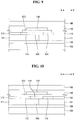
- a solar cell module according to a first comparative example is described below with reference to FIGS. 8 and 9 .
- the first embodiment of the invention electrically connects the interconnector 120 to the first electrode current collector 114 using the first conductive adhesive film CF1 and also electrically connects the interconnector 120 to the second electrode current collector 115 using the second conductive adhesive film CF2.
- the first comparative example electrically connects the interconnector 120 to the first and second electrode current collectors 114 and 115 using only a third conductive adhesive film CF3.
- Structures and components identical or equivalent to those in the first embodiment and first comparative example are designated with the same reference numerals, and a further description may be briefly made or may be entirely omitted.
- a width of the third conductive adhesive film CF3 in the second direction X-X' may be equal to or greater than a width of the interconnector 120, and a length of the third conductive adhesive film CF3 in the first direction Y-Y' may be equal to or greater than a length of the interconnector 120.
- the third conductive adhesive film CF3 may not contact first and second electrodes 112 and 113, and the interconnector 120 may have slits or holes 122.
- FIG. 9 Various modifications of the solar cell module shown in FIG. 9 are described below with reference to FIGS. 10 to 13 .
- the back encapsulant 140 extends from the front encapsulant 130 to the third conductive adhesive film CF3.
- the third conductive adhesive film CF3 may include a space supporter 170' performing a function similar to the spacer 170 according to the first embodiment of the invention.
- the third conductive adhesive film CF3 and the space supporter 170' may form an integral body.
- the integral formation means the space supporter 170' is formed of the same material as the third conductive adhesive film CF3.
- FIG. 10 shows that the space supporter 170' of the third conductive adhesive film CF3 contacts the crystalline semiconductor substrate 111. However, because the back protective layer 116b is positioned on the surface of the crystalline semiconductor substrate 111, the space supporter 170' does not directly contact the crystalline semiconductor substrate 111. In the solar cell module shown in FIG. 10 , the back encapsulant 140 extends from the front encapsulant 130 to the space supporter 170', and the space supporter 170' extends from the back encapsulant 140 to the third conductive adhesive film CF3.
- the solar cell module according to the first comparative example may include a spacer 170 in the same manner as the modifications of the first embodiment of the invention.
- the spacer 170 may be positioned between the adjacent first and second electrode current collectors 114 and 115.
- the back encapsulant 140 extends from the front encapsulant 130 to the spacer 170, and the spacer 170 extends from the back encapsulant 140 to the third conductive adhesive film CF3.
- the spacer 170 may be positioned between the two adjacent crystalline semiconductor substrates 111. In the solar cell module shown in FIG. 12 , the spacer 170 extends from the front encapsulant 130 to the back encapsulant 140, and the back encapsulant 140 extends from spacer 170 to the third conductive adhesive film CF3.
- the spacer 170 may be positioned between the two adjacent crystalline semiconductor substrates 111 and between the adjacent first and second electrode current collectors 114 and 115. In the solar cell module shown in FIG. 13 , the spacer 170 extends from the front encapsulant 130 to the third conductive adhesive film CF3.
- a thickness of the spacer 170 may be substantially equal to a thickness of each of the first and second electrode current collectors 114 and 115 or may be greater than the thickness of each of the first and second electrode current collectors 114 and 115.
- the third conductive adhesive film CF3 may have a groove H1 in which a portion of the spacer 170 is buried.
- the back encapsulant 140 When the back encapsulant 140 is formed of cured siloxane, the back encapsulant 140 may be filled in a space between the two adjacent crystalline semiconductor substrates 111.
- the front encapsulant 130 or both the front encapsulant 130 and the back encapsulant 140 may be filled in the space between the two adjacent crystalline semiconductor substrates 111.
- the spacer 170 when the spacer 170 is positioned between the two adjacent crystalline semiconductor substrates 111, the spacer 170 may have the same thickness as the crystalline semiconductor substrate 111.
- the back encapsulant 140 may be filled in a space between the spacer 170 and the third conductive adhesive film CF3.
- the front encapsulant 130 or both the front encapsulant 130 and the back encapsulant 140 may be filled in the space between the spacer 170 and the third conductive adhesive film CF3.
- a thickness of the spacer 170 may be equal to or greater than a sum of the thicknesses of the crystalline semiconductor substrate 111 and the first electrode current collector 114 and a sum of the thicknesses of the crystalline semiconductor substrate 111 and the second electrode current collector 115.
- the third conductive adhesive film CF3 may have a groove H1 in which a portion of the spacer 170 is buried.
- the distance and the electrical insulation between the adjacent back contact solar cells 110 are carried out by the spacer 170.
- the interconnector 120 may be viewed through a space between the adjacent back contact solar cells 110 when viewed at a light receiving surface of the solar cell module.
- the interconnector 120 is formed of conductive metal of a color different from the back contact solar cells 110.
- the surface of the spacer 170 toward the light receiving surface of the solar cell module may be processed in the same color (for example, black or white) as the crystalline semiconductor substrate 111 or the back sheet 160, so as to improve an appearance of the solar cell module.
- FIG. 14 is a plane view of a solar cell module according to a second comparative example in a state where a back sheet of the solar cell module is removed.
- Configuration of the solar cell module according to the second comparative example is substantially the same as the solar cell module according to the first comparative example, except adjacent back contact solar cells 110 are electrically connected to each other using a plurality of interconnectors 120.
- a portion of a third conductive adhesive film CF3 contacts a second electrode current collector 115 of a back contact solar cell 110 positioned on a left side thereof. Further, another portion of the third conductive adhesive film CF3 contacts a first electrode current collector 114 of a back contact solar cell 110 positioned on a right side thereof.
- At least two interconnectors 120 are positioned on the third conductive adhesive film CF3 in a longitudinal direction of the third conductive adhesive film CF3, i.e., in the first direction Y-Y'.
- the second comparative example using at least two interconnectors 120 may be equally applied to the first embodiment of the invention.
- FIG. 14 shows that the three interconnectors 120 are attached to one third conductive adhesive film CF3.
- a third conductive adhesive film CF3 may be divided into a plurality of parts in the same manner as interconnectors 120.
- a second electrode current collector 115 of one back contact solar cell 110 may be electrically connected to a first electrode current collector 114 of another back contact solar cell 110 adjacent to the one back contact solar cell 110 using at least two third conductive adhesive films CF3 and the interconnectors 120 having the same number as the number of third conductive adhesive films CF3.
- a second electrode current collector 115 of one back contact solar cell 110 and a first electrode current collector 114 of another back contact solar cell 110 adjacent to the one back contact solar cell 110 may contact at least two third conductive adhesive films CF3. Further, the at least two third conductive adhesive films CF3 may contact one interconnector 120.
- Each of the back contact solar cells 110 used in the solar cell module according to the embodiments of the invention and the comparative examples may have a non-bus bar structure in which there is no current collector, i.e., bus-bar.
- a first electrode part includes only a plurality of first electrodes extending in the second direction perpendicular to the first direction, and a second electrode part includes only a plurality of second electrodes extending in the second direction.
- the first electrodes and the second electrodes are alternately disposed.
- the first electrodes are not physically connected to one another because of an electrode material for forming the first electrodes
- the second electrodes are not physically connected to one another because of an electrode material for forming the second electrodes.
- the back contact solar cell 110 of the non-bus bar structure may reduce the manufacturing cost and the number of manufacturing steps resulting from the formation of the bus bar.
- a conductive adhesive film physically contacts one end of each of the first electrodes or one end of each of the second electrodes, and thus electrically connects the ends of the first electrodes to one another or electrically connects the ends of the second electrodes to one another.
- each first electrode and the one end of each second electrode may have a contact part of an extended width.
Landscapes
- Engineering & Computer Science (AREA)
- Life Sciences & Earth Sciences (AREA)
- General Physics & Mathematics (AREA)
- Physics & Mathematics (AREA)
- Condensed Matter Physics & Semiconductors (AREA)
- Electromagnetism (AREA)
- Sustainable Energy (AREA)
- Computer Hardware Design (AREA)
- Microelectronics & Electronic Packaging (AREA)
- Power Engineering (AREA)
- Sustainable Development (AREA)
- Chemical & Material Sciences (AREA)
- Crystallography & Structural Chemistry (AREA)
- Photovoltaic Devices (AREA)
Claims (7)
- Module de cellules solaires comprenant :une pluralité de cellules solaires à contact arrière (110) comprenant chacune un substrat semi-conducteur cristallin (111) formé d'un premier silicium de type conducteur, une couche de protection arrière (116b) sur une surface arrière du substrat (111), une pluralité de premières couches de silicium amorphes (119a) positionnées sur la couche de protection arrière (116b) servant de région émettrice (119a), et une pluralité de secondes couches de silicium amorphes (119b) qui sont positionnées sur la couche de protection arrière (116b) pour être séparées de la pluralité de premières couches de silicium amorphes (119a) servant de région de champ de surface arrière, BSF, (119b), un premier collecteur de courant d'électrode (114) qui est positionné au niveau d'un premier bord d'une surface arrière du substrat (111) et s'étend dans une première direction, une pluralité de premières électrodes (112) dont les premières extrémités sont reliées les unes aux autres à l'aide du premier collecteur de courant d'électrode (114), un second collecteur de courant d'électrode (115) qui est positionné au niveau d'un second bord de la surface arrière du substrat (111) et s'étend dans la première direction, et une pluralité de secondes électrodes (113) dont les premières extrémités sont reliées les unes aux autres à l'aide du second collecteur de courant d'électrode (115) ; etun premier film adhésif conducteur (CF1) en contact avec un premier collecteur de courant d'électrode (114) d'une première cellule solaire (110) de la pluralité de cellules solaires à contact arrière (110) ;un second film adhésif conducteur (CF2) en contact avec un second collecteur de courant d'électrode (115) d'une deuxième cellule solaire (110) adjacente à la première cellule solaire (110) ; etun interconnecteur (120) configuré pour mettre en contact les premier (CF1) et second (CF2) films adhésifs conducteurs et connecter électriquement les première (110) et deuxième (110) cellules solaires adjacentes l'une à l'autre,la pluralité de premières électrodes (112) et la pluralité de secondes électrodes (113) étant positionnées de manière alternée,la pluralité de premières électrodes (112) étant en contact avec la région émettrice (119a), et la pluralité de secondes électrodes (113) étant en contact avec la région de champ de surface arrière (119b),l'interconnecteur (120) étant en contact à la fois avec le premier film adhésif conducteur (CF1) et le second film adhésif conducteur (CF2),une longueur de l'interconnecteur (120) étant inférieure à une longueur du premier film adhésif conducteur (CF1) et à une longueur du second film adhésif conducteur (CF2),le premier film adhésif conducteur (CF1) et le second film adhésif conducteur (CF2) étant espacés d'une distance entre la première cellule solaire (110) et la deuxième cellule solaire (110), et une largeur de l'interconnecteur (120) étant supérieure à la distance entre des extrémités adjacentes du premier film adhésif conducteur (CF1) et du second film adhésif conducteur (CF2), etun élément d'espacement (170) étant positionné entre les première (110) et deuxième (110) cellules solaires adjacentes.
- Module de cellules solaires selon la revendication 1, dans lequel une largeur et la longueur du premier film adhésif conducteur (CF1) sont égales ou inférieures à une largeur et une longueur du premier collecteur de courant d'électrode (114), respectivement, et une largeur et la longueur du second film adhésif conducteur (CF2) sont égales ou inférieures à une largeur et une longueur du second collecteur de courant d'électrode (115), respectivement.
- Module de cellules solaires selon la revendication 1, dans lequel la pluralité de premières électrodes (112, 212) s'étendent dans une seconde direction perpendiculaire à la première direction et la pluralité de secondes électrodes (113) sont positionnées entre les premières électrodes (112) et s'étendent dans la seconde direction, etle premier film adhésif conducteur (CF1) n'est pas en contact avec la pluralité de premières électrodes (112), et le second film adhésif conducteur (CF2) n'est pas en contact avec la pluralité de secondes électrodes (113).
- Module de cellules solaires selon la revendication 1, comprenant en outre :un agent d'encapsulation avant (130) et un agent d'encapsulation arrière (140) configurés pour protéger la pluralité de cellules solaires (110) ;un élément transparent (150) positionné sur l'agent d'encapsulation avant (130) sur des surfaces avant des substrats (111) de la pluralité de cellules solaires (110) ; etune feuille arrière (160) positionnée sous l'agent d'encapsulation arrière (140) sur les surfaces arrière des substrats (111) de la pluralité de cellules solaires (110),l'élément d'espacement (170) étant positionné entre les substrats (111, 211) des première (110) et deuxième (110) cellules solaires adjacentes, etl'agent d'encapsulation avant (130) ou l'agent d'encapsulation arrière (140) étant rempli dans un espace entre l'élément d'espacement (170) et l'interconnecteur (120).
- Module de cellules solaires selon la revendication 1, comprenant en outre :un agent d'encapsulation avant (130) et un agent d'encapsulation arrière (140) configurés pour protéger la pluralité de cellules solaires (110) ;un élément transparent (150) positionné sur l'agent d'encapsulation avant (130) sur des surfaces avant des substrats (111) de la pluralité de cellules solaires (110) ; etune feuille arrière (160) positionnée sous l'agent d'encapsulation arrière (140) sur les surfaces arrière des substrats (111, 211) de la pluralité de cellules solaires (110),l'élément d'espacement (170) étant positionné entre le premier collecteur de courant d'électrode (114) de la première cellule solaire (110) et le second collecteur de courant d'électrode (115) de la deuxième cellule solaire (110), etl'agent d'encapsulation avant (130) ou l'agent d'encapsulation arrière (140) étant rempli dans un espace entre les substrats (111) des première (110) et deuxième (110) cellules solaires adjacentes.
- Module de cellules solaires selon la revendication 1, dans lequel l'élément d'espacement (170) est positionné entre les substrats (111) des première (110) et deuxième (110) cellules solaires adjacentes et entre le premier collecteur de courant d'électrode (114) de la première cellule solaire (110) et le second collecteur de courant d'électrode (115) de la deuxième cellule solaire (110).
- Module de cellules solaires selon la revendication 1, comprenant en outre :un agent d'encapsulation avant (130) et un agent d'encapsulation arrière (140) configurés pour protéger la pluralité de cellules solaires (110) ;un élément transparent (150) positionné sur l'agent d'encapsulation avant (130) sur des surfaces avant des substrats (111) de la pluralité de cellules solaires (110) ; etune feuille arrière (160) positionnée sous l'agent d'encapsulation arrière (140) sur les surfaces arrière des substrats (111) de la pluralité de cellules solaires (110),l'élément d'espacement (170) ayant sensiblement la même épaisseur que le substrat (111) de chaque cellule solaire (110), etl'agent d'encapsulation avant (130) ou l'agent d'encapsulation arrière (140) étant rempli dans un espace entre l'élément d'espacement (170) et l'interconnecteur (120).
Applications Claiming Priority (2)
| Application Number | Priority Date | Filing Date | Title |
|---|---|---|---|
| KR1020110098998A KR101282939B1 (ko) | 2011-09-29 | 2011-09-29 | 태양전지 모듈 |
| KR1020110099000A KR101223050B1 (ko) | 2011-09-29 | 2011-09-29 | 태양전지 모듈 |
Publications (3)
| Publication Number | Publication Date |
|---|---|
| EP2575184A2 EP2575184A2 (fr) | 2013-04-03 |
| EP2575184A3 EP2575184A3 (fr) | 2014-10-22 |
| EP2575184B1 true EP2575184B1 (fr) | 2017-12-06 |
Family
ID=47010143
Family Applications (1)
| Application Number | Title | Priority Date | Filing Date |
|---|---|---|---|
| EP12006599.0A Not-in-force EP2575184B1 (fr) | 2011-09-29 | 2012-09-20 | Module de cellule solaire |
Country Status (4)
| Country | Link |
|---|---|
| US (1) | US9490376B2 (fr) |
| EP (1) | EP2575184B1 (fr) |
| JP (1) | JP6224307B2 (fr) |
| CN (1) | CN103035763A (fr) |
Families Citing this family (19)
| Publication number | Priority date | Publication date | Assignee | Title |
|---|---|---|---|---|
| KR101890324B1 (ko) * | 2012-06-22 | 2018-09-28 | 엘지전자 주식회사 | 태양 전지 모듈 및 이에 적용되는 리본 결합체 |
| KR102087156B1 (ko) * | 2013-07-09 | 2020-03-10 | 엘지전자 주식회사 | 태양전지 모듈 |
| KR102124520B1 (ko) * | 2013-10-29 | 2020-06-18 | 엘지전자 주식회사 | 태양 전지 모듈 및 그 제조 방법 |
| KR102319721B1 (ko) | 2013-10-29 | 2021-11-01 | 엘지전자 주식회사 | 태양 전지 및 태양 전지 모듈 |
| KR102175893B1 (ko) | 2014-02-24 | 2020-11-06 | 엘지전자 주식회사 | 태양 전지 모듈의 제조 방법 |
| KR102271055B1 (ko) * | 2014-06-26 | 2021-07-01 | 엘지전자 주식회사 | 태양 전지 모듈 |
| EP3159934B1 (fr) * | 2014-09-30 | 2018-03-21 | LG Electronics Inc. | Panneau de cellule solaire |
| KR20160064692A (ko) * | 2014-11-28 | 2016-06-08 | 엘지전자 주식회사 | 태양 전지 및 그 제조 방법 |
| JPWO2016103625A1 (ja) * | 2014-12-26 | 2017-09-14 | パナソニックIpマネジメント株式会社 | 太陽電池モジュール |
| TWI538230B (zh) * | 2015-03-23 | 2016-06-11 | 茂迪股份有限公司 | 背接觸太陽能電池組及其製造方法 |
| US10535790B2 (en) * | 2015-06-25 | 2020-01-14 | Sunpower Corporation | One-dimensional metallization for solar cells |
| EP3151288B1 (fr) * | 2015-10-02 | 2019-12-04 | LG Electronics Inc. | Appareil de fixation de l'interconnecteur d'un panneau de cellules solaires |
| CN106229352A (zh) * | 2016-09-06 | 2016-12-14 | 浙江晶科能源有限公司 | 一种ibc结构太阳能电池及其制备方法 |
| JP7076376B2 (ja) * | 2016-12-08 | 2022-05-27 | 株式会社カネカ | 太陽電池モジュール |
| CN109888045B (zh) * | 2019-03-29 | 2023-07-25 | 通威太阳能(成都)有限公司 | 一种新型双面perc叠瓦电池片及其制备方法 |
| CN110246911A (zh) * | 2019-05-30 | 2019-09-17 | 泰州隆基乐叶光伏科技有限公司 | 背接触叠片太阳电池串及制造方法、叠片太阳电池组件 |
| JP7433340B2 (ja) * | 2019-12-11 | 2024-02-19 | 株式会社カネカ | 太陽電池セル、太陽電池デバイスおよび太陽電池モジュール |
| CN111799348A (zh) * | 2020-06-10 | 2020-10-20 | 中国科学院微电子研究所 | 一种异质结背接触太阳能电池及其形成方法 |
| CN113327997A (zh) | 2021-07-15 | 2021-08-31 | 浙江爱旭太阳能科技有限公司 | 一种背接触太阳能电池串及制备方法、组件及系统 |
Citations (2)
| Publication number | Priority date | Publication date | Assignee | Title |
|---|---|---|---|---|
| WO2003083955A1 (fr) * | 2002-03-29 | 2003-10-09 | Ebara Corporation | Element photovoltaique et procede de fabrication |
| US20090038675A1 (en) * | 2007-08-07 | 2009-02-12 | Sanyo Electric Co., Ltd. | Solar cell module |
Family Cites Families (21)
| Publication number | Priority date | Publication date | Assignee | Title |
|---|---|---|---|---|
| US5951786A (en) | 1997-12-19 | 1999-09-14 | Sandia Corporation | Laminated photovoltaic modules using back-contact solar cells |
| US20050172996A1 (en) * | 2004-02-05 | 2005-08-11 | Advent Solar, Inc. | Contact fabrication of emitter wrap-through back contact silicon solar cells |
| US7390961B2 (en) | 2004-06-04 | 2008-06-24 | Sunpower Corporation | Interconnection of solar cells in a solar cell module |
| JP2006324590A (ja) | 2005-05-20 | 2006-11-30 | Sharp Corp | 裏面電極型太陽電池とその製造方法 |
| EP2100336A4 (fr) * | 2006-12-22 | 2013-04-10 | Applied Materials Inc | Technologies d'interconnexion pour cellules et modules solaires a contact arriere |
| WO2008090718A1 (fr) | 2007-01-25 | 2008-07-31 | Sharp Kabushiki Kaisha | Cellule de batterie solaire, réseau de batteries solaires, module de batterie solaire et procédé de fabrication d'un réseau de batteries solaires |
| JP4894920B2 (ja) * | 2007-05-09 | 2012-03-14 | 日立化成工業株式会社 | 導電体の接続方法、導電体接続用部材、接続構造及び太陽電池モジュール |
| JP5116363B2 (ja) | 2007-05-29 | 2013-01-09 | デクセリアルズ株式会社 | 導体線の製造方法 |
| JP2009130116A (ja) | 2007-11-22 | 2009-06-11 | Sharp Corp | 素子間配線部材、光電変換素子およびこれらを用いた光電変換素子接続体ならびに光電変換モジュール |
| JP2009176782A (ja) | 2008-01-21 | 2009-08-06 | Sanyo Electric Co Ltd | 太陽電池モジュール |
| JP2009290105A (ja) | 2008-05-30 | 2009-12-10 | Sharp Corp | 太陽電池、太陽電池の製造方法および太陽電池モジュール |
| JP2009302327A (ja) | 2008-06-13 | 2009-12-24 | Sharp Corp | 配線部材の接続構造およびそれを備えた太陽電池モジュールならびにその製造方法 |
| JP2012501551A (ja) * | 2008-08-27 | 2012-01-19 | アプライド マテリアルズ インコーポレイテッド | バックコンタクト式太陽電池モジュール |
| JP2010251667A (ja) | 2009-04-20 | 2010-11-04 | Sanyo Electric Co Ltd | 太陽電池 |
| KR101586085B1 (ko) | 2009-05-14 | 2016-01-22 | 엘지전자 주식회사 | 태양 전지 모듈 및 그 제조 방법 |
| KR101295541B1 (ko) | 2009-05-14 | 2013-08-12 | 엘지전자 주식회사 | 태양 전지 모듈 및 그 제조 방법 |
| KR101130197B1 (ko) * | 2009-09-28 | 2012-03-30 | 엘지전자 주식회사 | 태양전지 모듈 및 그 제조 방법 |
| EP2601687A4 (fr) * | 2010-08-05 | 2018-03-07 | Solexel, Inc. | Renforcement de plan arrière et interconnexions pour cellules solaires |
| KR101045860B1 (ko) | 2010-08-11 | 2011-07-01 | 엘지전자 주식회사 | 태양전지 패널 |
| JP2012084560A (ja) | 2010-10-06 | 2012-04-26 | Hitachi High-Technologies Corp | 結晶系太陽電池モジュール |
| JP5892584B2 (ja) | 2011-09-26 | 2016-03-23 | デクセリアルズ株式会社 | 太陽電池モジュール、太陽電池モジュールの製造方法 |
-
2012
- 2012-09-14 US US13/617,784 patent/US9490376B2/en not_active Expired - Fee Related
- 2012-09-20 EP EP12006599.0A patent/EP2575184B1/fr not_active Not-in-force
- 2012-09-27 JP JP2012213477A patent/JP6224307B2/ja not_active Expired - Fee Related
- 2012-09-28 CN CN2012103679458A patent/CN103035763A/zh active Pending
Patent Citations (2)
| Publication number | Priority date | Publication date | Assignee | Title |
|---|---|---|---|---|
| WO2003083955A1 (fr) * | 2002-03-29 | 2003-10-09 | Ebara Corporation | Element photovoltaique et procede de fabrication |
| US20090038675A1 (en) * | 2007-08-07 | 2009-02-12 | Sanyo Electric Co., Ltd. | Solar cell module |
Also Published As
| Publication number | Publication date |
|---|---|
| EP2575184A3 (fr) | 2014-10-22 |
| CN103035763A (zh) | 2013-04-10 |
| JP6224307B2 (ja) | 2017-11-01 |
| EP2575184A2 (fr) | 2013-04-03 |
| JP2013077820A (ja) | 2013-04-25 |
| US9490376B2 (en) | 2016-11-08 |
| US20130081675A1 (en) | 2013-04-04 |
Similar Documents
| Publication | Publication Date | Title |
|---|---|---|
| EP2575184B1 (fr) | Module de cellule solaire | |
| EP2575183B1 (fr) | Module de cellule solaire | |
| KR101282939B1 (ko) | 태양전지 모듈 | |
| US9147787B2 (en) | Solar cell panel | |
| EP2528109A1 (fr) | Module de cellule solaire | |
| US9917223B2 (en) | Solar cell panel | |
| EP2535950B1 (fr) | Module de cellule solaire | |
| US9385256B2 (en) | Solar cell panel | |
| US20140238462A1 (en) | Solar cell module | |
| US8975507B2 (en) | Solar cell module | |
| KR101223050B1 (ko) | 태양전지 모듈 | |
| KR20120124570A (ko) | 태양 전지 모듈 및 이에 사용되는 도전성 접착 필름 | |
| KR101235339B1 (ko) | 태양전지 모듈 | |
| KR101692560B1 (ko) | 태양전지 모듈 | |
| KR101642154B1 (ko) | 태양전지 패널 및 이의 제조 방법 |
Legal Events
| Date | Code | Title | Description |
|---|---|---|---|
| PUAI | Public reference made under article 153(3) epc to a published international application that has entered the european phase |
Free format text: ORIGINAL CODE: 0009012 |
|
| 17P | Request for examination filed |
Effective date: 20120920 |
|
| AK | Designated contracting states |
Kind code of ref document: A2 Designated state(s): AL AT BE BG CH CY CZ DE DK EE ES FI FR GB GR HR HU IE IS IT LI LT LU LV MC MK MT NL NO PL PT RO RS SE SI SK SM TR |
|
| AX | Request for extension of the european patent |
Extension state: BA ME |
|
| PUAL | Search report despatched |
Free format text: ORIGINAL CODE: 0009013 |
|
| AK | Designated contracting states |
Kind code of ref document: A3 Designated state(s): AL AT BE BG CH CY CZ DE DK EE ES FI FR GB GR HR HU IE IS IT LI LT LU LV MC MK MT NL NO PL PT RO RS SE SI SK SM TR |
|
| AX | Request for extension of the european patent |
Extension state: BA ME |
|
| RIC1 | Information provided on ipc code assigned before grant |
Ipc: H01L 31/0224 20060101ALI20140918BHEP Ipc: H01L 31/05 20140101ALI20140918BHEP Ipc: H01L 31/068 20120101ALI20140918BHEP Ipc: H01L 31/0747 20120101AFI20140918BHEP |
|
| 17Q | First examination report despatched |
Effective date: 20150520 |
|
| GRAP | Despatch of communication of intention to grant a patent |
Free format text: ORIGINAL CODE: EPIDOSNIGR1 |
|
| STAA | Information on the status of an ep patent application or granted ep patent |
Free format text: STATUS: GRANT OF PATENT IS INTENDED |
|
| INTG | Intention to grant announced |
Effective date: 20170707 |
|
| RIN1 | Information on inventor provided before grant (corrected) |
Inventor name: JOE, JINHYOUN Inventor name: CHOI, JUNGHOON Inventor name: JI, KWANGSUN |
|
| GRAS | Grant fee paid |
Free format text: ORIGINAL CODE: EPIDOSNIGR3 |
|
| GRAA | (expected) grant |
Free format text: ORIGINAL CODE: 0009210 |
|
| STAA | Information on the status of an ep patent application or granted ep patent |
Free format text: STATUS: THE PATENT HAS BEEN GRANTED |
|
| AK | Designated contracting states |
Kind code of ref document: B1 Designated state(s): AL AT BE BG CH CY CZ DE DK EE ES FI FR GB GR HR HU IE IS IT LI LT LU LV MC MK MT NL NO PL PT RO RS SE SI SK SM TR |
|
| REG | Reference to a national code |
Ref country code: GB Ref legal event code: FG4D |
|
| REG | Reference to a national code |
Ref country code: AT Ref legal event code: REF Ref document number: 953113 Country of ref document: AT Kind code of ref document: T Effective date: 20171215 Ref country code: CH Ref legal event code: EP |
|
| REG | Reference to a national code |
Ref country code: IE Ref legal event code: FG4D |
|
| REG | Reference to a national code |
Ref country code: NL Ref legal event code: FP |
|
| REG | Reference to a national code |
Ref country code: DE Ref legal event code: R096 Ref document number: 602012040489 Country of ref document: DE |
|
| REG | Reference to a national code |
Ref country code: LT Ref legal event code: MG4D |
|
| PG25 | Lapsed in a contracting state [announced via postgrant information from national office to epo] |
Ref country code: SE Free format text: LAPSE BECAUSE OF FAILURE TO SUBMIT A TRANSLATION OF THE DESCRIPTION OR TO PAY THE FEE WITHIN THE PRESCRIBED TIME-LIMIT Effective date: 20171206 Ref country code: LT Free format text: LAPSE BECAUSE OF FAILURE TO SUBMIT A TRANSLATION OF THE DESCRIPTION OR TO PAY THE FEE WITHIN THE PRESCRIBED TIME-LIMIT Effective date: 20171206 Ref country code: NO Free format text: LAPSE BECAUSE OF FAILURE TO SUBMIT A TRANSLATION OF THE DESCRIPTION OR TO PAY THE FEE WITHIN THE PRESCRIBED TIME-LIMIT Effective date: 20180306 Ref country code: ES Free format text: LAPSE BECAUSE OF FAILURE TO SUBMIT A TRANSLATION OF THE DESCRIPTION OR TO PAY THE FEE WITHIN THE PRESCRIBED TIME-LIMIT Effective date: 20171206 Ref country code: FI Free format text: LAPSE BECAUSE OF FAILURE TO SUBMIT A TRANSLATION OF THE DESCRIPTION OR TO PAY THE FEE WITHIN THE PRESCRIBED TIME-LIMIT Effective date: 20171206 |
|
| REG | Reference to a national code |
Ref country code: AT Ref legal event code: MK05 Ref document number: 953113 Country of ref document: AT Kind code of ref document: T Effective date: 20171206 |
|
| PG25 | Lapsed in a contracting state [announced via postgrant information from national office to epo] |
Ref country code: RS Free format text: LAPSE BECAUSE OF FAILURE TO SUBMIT A TRANSLATION OF THE DESCRIPTION OR TO PAY THE FEE WITHIN THE PRESCRIBED TIME-LIMIT Effective date: 20171206 Ref country code: LV Free format text: LAPSE BECAUSE OF FAILURE TO SUBMIT A TRANSLATION OF THE DESCRIPTION OR TO PAY THE FEE WITHIN THE PRESCRIBED TIME-LIMIT Effective date: 20171206 Ref country code: BG Free format text: LAPSE BECAUSE OF FAILURE TO SUBMIT A TRANSLATION OF THE DESCRIPTION OR TO PAY THE FEE WITHIN THE PRESCRIBED TIME-LIMIT Effective date: 20180306 Ref country code: GR Free format text: LAPSE BECAUSE OF FAILURE TO SUBMIT A TRANSLATION OF THE DESCRIPTION OR TO PAY THE FEE WITHIN THE PRESCRIBED TIME-LIMIT Effective date: 20180307 Ref country code: HR Free format text: LAPSE BECAUSE OF FAILURE TO SUBMIT A TRANSLATION OF THE DESCRIPTION OR TO PAY THE FEE WITHIN THE PRESCRIBED TIME-LIMIT Effective date: 20171206 |
|
| PG25 | Lapsed in a contracting state [announced via postgrant information from national office to epo] |
Ref country code: SK Free format text: LAPSE BECAUSE OF FAILURE TO SUBMIT A TRANSLATION OF THE DESCRIPTION OR TO PAY THE FEE WITHIN THE PRESCRIBED TIME-LIMIT Effective date: 20171206 Ref country code: EE Free format text: LAPSE BECAUSE OF FAILURE TO SUBMIT A TRANSLATION OF THE DESCRIPTION OR TO PAY THE FEE WITHIN THE PRESCRIBED TIME-LIMIT Effective date: 20171206 Ref country code: CZ Free format text: LAPSE BECAUSE OF FAILURE TO SUBMIT A TRANSLATION OF THE DESCRIPTION OR TO PAY THE FEE WITHIN THE PRESCRIBED TIME-LIMIT Effective date: 20171206 |
|
| PG25 | Lapsed in a contracting state [announced via postgrant information from national office to epo] |
Ref country code: SM Free format text: LAPSE BECAUSE OF FAILURE TO SUBMIT A TRANSLATION OF THE DESCRIPTION OR TO PAY THE FEE WITHIN THE PRESCRIBED TIME-LIMIT Effective date: 20171206 Ref country code: AT Free format text: LAPSE BECAUSE OF FAILURE TO SUBMIT A TRANSLATION OF THE DESCRIPTION OR TO PAY THE FEE WITHIN THE PRESCRIBED TIME-LIMIT Effective date: 20171206 Ref country code: PL Free format text: LAPSE BECAUSE OF FAILURE TO SUBMIT A TRANSLATION OF THE DESCRIPTION OR TO PAY THE FEE WITHIN THE PRESCRIBED TIME-LIMIT Effective date: 20171206 Ref country code: RO Free format text: LAPSE BECAUSE OF FAILURE TO SUBMIT A TRANSLATION OF THE DESCRIPTION OR TO PAY THE FEE WITHIN THE PRESCRIBED TIME-LIMIT Effective date: 20171206 |
|
| REG | Reference to a national code |
Ref country code: DE Ref legal event code: R097 Ref document number: 602012040489 Country of ref document: DE |
|
| PLBE | No opposition filed within time limit |
Free format text: ORIGINAL CODE: 0009261 |
|
| STAA | Information on the status of an ep patent application or granted ep patent |
Free format text: STATUS: NO OPPOSITION FILED WITHIN TIME LIMIT |
|
| PGFP | Annual fee paid to national office [announced via postgrant information from national office to epo] |
Ref country code: DE Payment date: 20180806 Year of fee payment: 7 |
|
| 26N | No opposition filed |
Effective date: 20180907 |
|
| PG25 | Lapsed in a contracting state [announced via postgrant information from national office to epo] |
Ref country code: SI Free format text: LAPSE BECAUSE OF FAILURE TO SUBMIT A TRANSLATION OF THE DESCRIPTION OR TO PAY THE FEE WITHIN THE PRESCRIBED TIME-LIMIT Effective date: 20171206 Ref country code: DK Free format text: LAPSE BECAUSE OF FAILURE TO SUBMIT A TRANSLATION OF THE DESCRIPTION OR TO PAY THE FEE WITHIN THE PRESCRIBED TIME-LIMIT Effective date: 20171206 |
|
| PG25 | Lapsed in a contracting state [announced via postgrant information from national office to epo] |
Ref country code: MC Free format text: LAPSE BECAUSE OF FAILURE TO SUBMIT A TRANSLATION OF THE DESCRIPTION OR TO PAY THE FEE WITHIN THE PRESCRIBED TIME-LIMIT Effective date: 20171206 |
|
| REG | Reference to a national code |
Ref country code: CH Ref legal event code: PL |
|
| REG | Reference to a national code |
Ref country code: NL Ref legal event code: MM Effective date: 20181001 |
|
| GBPC | Gb: european patent ceased through non-payment of renewal fee |
Effective date: 20180920 |
|
| REG | Reference to a national code |
Ref country code: BE Ref legal event code: MM Effective date: 20180930 |
|
| REG | Reference to a national code |
Ref country code: IE Ref legal event code: MM4A |
|
| PG25 | Lapsed in a contracting state [announced via postgrant information from national office to epo] |
Ref country code: LU Free format text: LAPSE BECAUSE OF NON-PAYMENT OF DUE FEES Effective date: 20180920 Ref country code: NL Free format text: LAPSE BECAUSE OF NON-PAYMENT OF DUE FEES Effective date: 20181001 |
|
| PG25 | Lapsed in a contracting state [announced via postgrant information from national office to epo] |
Ref country code: IT Free format text: LAPSE BECAUSE OF NON-PAYMENT OF DUE FEES Effective date: 20180920 Ref country code: IE Free format text: LAPSE BECAUSE OF NON-PAYMENT OF DUE FEES Effective date: 20180920 |
|
| PG25 | Lapsed in a contracting state [announced via postgrant information from national office to epo] |
Ref country code: BE Free format text: LAPSE BECAUSE OF NON-PAYMENT OF DUE FEES Effective date: 20180930 Ref country code: FR Free format text: LAPSE BECAUSE OF NON-PAYMENT OF DUE FEES Effective date: 20180930 Ref country code: LI Free format text: LAPSE BECAUSE OF NON-PAYMENT OF DUE FEES Effective date: 20180930 Ref country code: CH Free format text: LAPSE BECAUSE OF NON-PAYMENT OF DUE FEES Effective date: 20180930 |
|
| PG25 | Lapsed in a contracting state [announced via postgrant information from national office to epo] |
Ref country code: GB Free format text: LAPSE BECAUSE OF NON-PAYMENT OF DUE FEES Effective date: 20180920 |
|
| PG25 | Lapsed in a contracting state [announced via postgrant information from national office to epo] |
Ref country code: MT Free format text: LAPSE BECAUSE OF NON-PAYMENT OF DUE FEES Effective date: 20180920 |
|
| PG25 | Lapsed in a contracting state [announced via postgrant information from national office to epo] |
Ref country code: TR Free format text: LAPSE BECAUSE OF FAILURE TO SUBMIT A TRANSLATION OF THE DESCRIPTION OR TO PAY THE FEE WITHIN THE PRESCRIBED TIME-LIMIT Effective date: 20171206 |
|
| REG | Reference to a national code |
Ref country code: DE Ref legal event code: R119 Ref document number: 602012040489 Country of ref document: DE |
|
| PG25 | Lapsed in a contracting state [announced via postgrant information from national office to epo] |
Ref country code: HU Free format text: LAPSE BECAUSE OF FAILURE TO SUBMIT A TRANSLATION OF THE DESCRIPTION OR TO PAY THE FEE WITHIN THE PRESCRIBED TIME-LIMIT; INVALID AB INITIO Effective date: 20120920 Ref country code: PT Free format text: LAPSE BECAUSE OF FAILURE TO SUBMIT A TRANSLATION OF THE DESCRIPTION OR TO PAY THE FEE WITHIN THE PRESCRIBED TIME-LIMIT Effective date: 20171206 |
|
| PG25 | Lapsed in a contracting state [announced via postgrant information from national office to epo] |
Ref country code: CY Free format text: LAPSE BECAUSE OF FAILURE TO SUBMIT A TRANSLATION OF THE DESCRIPTION OR TO PAY THE FEE WITHIN THE PRESCRIBED TIME-LIMIT Effective date: 20171206 Ref country code: MK Free format text: LAPSE BECAUSE OF NON-PAYMENT OF DUE FEES Effective date: 20171206 |
|
| PG25 | Lapsed in a contracting state [announced via postgrant information from national office to epo] |
Ref country code: AL Free format text: LAPSE BECAUSE OF FAILURE TO SUBMIT A TRANSLATION OF THE DESCRIPTION OR TO PAY THE FEE WITHIN THE PRESCRIBED TIME-LIMIT Effective date: 20171206 Ref country code: DE Free format text: LAPSE BECAUSE OF NON-PAYMENT OF DUE FEES Effective date: 20200401 Ref country code: IS Free format text: LAPSE BECAUSE OF FAILURE TO SUBMIT A TRANSLATION OF THE DESCRIPTION OR TO PAY THE FEE WITHIN THE PRESCRIBED TIME-LIMIT Effective date: 20180406 |