WO2023228896A1 - 太陽電池モジュール - Google Patents
太陽電池モジュール Download PDFInfo
- Publication number
- WO2023228896A1 WO2023228896A1 PCT/JP2023/018912 JP2023018912W WO2023228896A1 WO 2023228896 A1 WO2023228896 A1 WO 2023228896A1 JP 2023018912 W JP2023018912 W JP 2023018912W WO 2023228896 A1 WO2023228896 A1 WO 2023228896A1
- Authority
- WO
- WIPO (PCT)
- Prior art keywords
- solar cell
- protective layer
- cell module
- electrode
- along
- Prior art date
Links
- 239000011241 protective layer Substances 0.000 claims abstract description 180
- 229920005989 resin Polymers 0.000 claims abstract description 50
- 239000011347 resin Substances 0.000 claims abstract description 50
- 239000000945 filler Substances 0.000 claims description 80
- 239000000463 material Substances 0.000 abstract description 77
- 238000011049 filling Methods 0.000 abstract description 3
- 239000004065 semiconductor Substances 0.000 description 80
- 239000010408 film Substances 0.000 description 66
- 239000000758 substrate Substances 0.000 description 59
- 238000000034 method Methods 0.000 description 46
- 238000004519 manufacturing process Methods 0.000 description 40
- 229910052709 silver Inorganic materials 0.000 description 34
- 239000004332 silver Substances 0.000 description 34
- BQCADISMDOOEFD-UHFFFAOYSA-N Silver Chemical compound [Ag] BQCADISMDOOEFD-UHFFFAOYSA-N 0.000 description 33
- 238000010586 diagram Methods 0.000 description 30
- 238000010248 power generation Methods 0.000 description 27
- 238000002161 passivation Methods 0.000 description 26
- 229910052782 aluminium Inorganic materials 0.000 description 25
- XAGFODPZIPBFFR-UHFFFAOYSA-N aluminium Chemical compound [Al] XAGFODPZIPBFFR-UHFFFAOYSA-N 0.000 description 25
- 230000001681 protective effect Effects 0.000 description 20
- 230000015572 biosynthetic process Effects 0.000 description 14
- 238000003475 lamination Methods 0.000 description 14
- 229910052751 metal Inorganic materials 0.000 description 13
- 239000002184 metal Substances 0.000 description 13
- 239000011521 glass Substances 0.000 description 11
- 239000005038 ethylene vinyl acetate Substances 0.000 description 10
- 229920001200 poly(ethylene-vinyl acetate) Polymers 0.000 description 10
- 239000010409 thin film Substances 0.000 description 10
- YCKRFDGAMUMZLT-UHFFFAOYSA-N Fluorine atom Chemical compound [F] YCKRFDGAMUMZLT-UHFFFAOYSA-N 0.000 description 9
- 150000001875 compounds Chemical class 0.000 description 9
- 239000000428 dust Substances 0.000 description 9
- 239000007772 electrode material Substances 0.000 description 9
- 238000010304 firing Methods 0.000 description 9
- 229910052731 fluorine Inorganic materials 0.000 description 9
- 239000011737 fluorine Substances 0.000 description 9
- 230000008569 process Effects 0.000 description 9
- 239000000243 solution Substances 0.000 description 9
- 238000009792 diffusion process Methods 0.000 description 8
- TWNQGVIAIRXVLR-UHFFFAOYSA-N oxo(oxoalumanyloxy)alumane Chemical compound O=[Al]O[Al]=O TWNQGVIAIRXVLR-UHFFFAOYSA-N 0.000 description 8
- 239000012783 reinforcing fiber Substances 0.000 description 8
- 238000007650 screen-printing Methods 0.000 description 8
- 239000002253 acid Substances 0.000 description 7
- 238000001035 drying Methods 0.000 description 7
- 239000010410 layer Substances 0.000 description 7
- IJGRMHOSHXDMSA-UHFFFAOYSA-N Atomic nitrogen Chemical compound N#N IJGRMHOSHXDMSA-UHFFFAOYSA-N 0.000 description 6
- HEMHJVSKTPXQMS-UHFFFAOYSA-M Sodium hydroxide Chemical compound [OH-].[Na+] HEMHJVSKTPXQMS-UHFFFAOYSA-M 0.000 description 6
- 229910001873 dinitrogen Inorganic materials 0.000 description 6
- 239000007789 gas Substances 0.000 description 6
- 238000010438 heat treatment Methods 0.000 description 6
- 239000002994 raw material Substances 0.000 description 6
- 229920001780 ECTFE Polymers 0.000 description 5
- 238000010030 laminating Methods 0.000 description 5
- 239000007800 oxidant agent Substances 0.000 description 5
- 238000003825 pressing Methods 0.000 description 5
- 239000004812 Fluorinated ethylene propylene Substances 0.000 description 4
- XUIMIQQOPSSXEZ-UHFFFAOYSA-N Silicon Chemical compound [Si] XUIMIQQOPSSXEZ-UHFFFAOYSA-N 0.000 description 4
- 239000007864 aqueous solution Substances 0.000 description 4
- 238000000231 atomic layer deposition Methods 0.000 description 4
- 238000006243 chemical reaction Methods 0.000 description 4
- 239000010949 copper Substances 0.000 description 4
- 229920000840 ethylene tetrafluoroethylene copolymer Polymers 0.000 description 4
- 230000006872 improvement Effects 0.000 description 4
- 238000002844 melting Methods 0.000 description 4
- 230000008018 melting Effects 0.000 description 4
- 229920009441 perflouroethylene propylene Polymers 0.000 description 4
- 238000000623 plasma-assisted chemical vapour deposition Methods 0.000 description 4
- 239000011669 selenium Substances 0.000 description 4
- 229910052710 silicon Inorganic materials 0.000 description 4
- 239000010703 silicon Substances 0.000 description 4
- 229910000679 solder Inorganic materials 0.000 description 4
- 239000002344 surface layer Substances 0.000 description 4
- JLTRXTDYQLMHGR-UHFFFAOYSA-N trimethylaluminium Chemical compound C[Al](C)C JLTRXTDYQLMHGR-UHFFFAOYSA-N 0.000 description 4
- XLYOFNOQVPJJNP-UHFFFAOYSA-N water Substances O XLYOFNOQVPJJNP-UHFFFAOYSA-N 0.000 description 4
- QTBSBXVTEAMEQO-UHFFFAOYSA-N Acetic acid Chemical compound CC(O)=O QTBSBXVTEAMEQO-UHFFFAOYSA-N 0.000 description 3
- QGZKDVFQNNGYKY-UHFFFAOYSA-N Ammonia Chemical compound N QGZKDVFQNNGYKY-UHFFFAOYSA-N 0.000 description 3
- RYGMFSIKBFXOCR-UHFFFAOYSA-N Copper Chemical compound [Cu] RYGMFSIKBFXOCR-UHFFFAOYSA-N 0.000 description 3
- -1 EVA and PVB Chemical class 0.000 description 3
- KWYUFKZDYYNOTN-UHFFFAOYSA-M Potassium hydroxide Chemical compound [OH-].[K+] KWYUFKZDYYNOTN-UHFFFAOYSA-M 0.000 description 3
- 229910052802 copper Inorganic materials 0.000 description 3
- KPUWHANPEXNPJT-UHFFFAOYSA-N disiloxane Chemical class [SiH3]O[SiH3] KPUWHANPEXNPJT-UHFFFAOYSA-N 0.000 description 3
- 238000005530 etching Methods 0.000 description 3
- 125000002887 hydroxy group Chemical group [H]O* 0.000 description 3
- 229910052738 indium Inorganic materials 0.000 description 3
- 229920002037 poly(vinyl butyral) polymer Polymers 0.000 description 3
- 239000000126 substance Substances 0.000 description 3
- 239000012808 vapor phase Substances 0.000 description 3
- CHJAYYWUZLWNSQ-UHFFFAOYSA-N 1-chloro-1,2,2-trifluoroethene;ethene Chemical group C=C.FC(F)=C(F)Cl CHJAYYWUZLWNSQ-UHFFFAOYSA-N 0.000 description 2
- MARUHZGHZWCEQU-UHFFFAOYSA-N 5-phenyl-2h-tetrazole Chemical compound C1=CC=CC=C1C1=NNN=N1 MARUHZGHZWCEQU-UHFFFAOYSA-N 0.000 description 2
- KRHYYFGTRYWZRS-UHFFFAOYSA-N Fluorane Chemical compound F KRHYYFGTRYWZRS-UHFFFAOYSA-N 0.000 description 2
- VZCYOOQTPOCHFL-OWOJBTEDSA-N Fumaric acid Chemical compound OC(=O)\C=C\C(O)=O VZCYOOQTPOCHFL-OWOJBTEDSA-N 0.000 description 2
- GYHNNYVSQQEPJS-UHFFFAOYSA-N Gallium Chemical compound [Ga] GYHNNYVSQQEPJS-UHFFFAOYSA-N 0.000 description 2
- OAICVXFJPJFONN-UHFFFAOYSA-N Phosphorus Chemical compound [P] OAICVXFJPJFONN-UHFFFAOYSA-N 0.000 description 2
- BUGBHKTXTAQXES-UHFFFAOYSA-N Selenium Chemical compound [Se] BUGBHKTXTAQXES-UHFFFAOYSA-N 0.000 description 2
- 229910052581 Si3N4 Inorganic materials 0.000 description 2
- BLRPTPMANUNPDV-UHFFFAOYSA-N Silane Chemical compound [SiH4] BLRPTPMANUNPDV-UHFFFAOYSA-N 0.000 description 2
- DHKHKXVYLBGOIT-UHFFFAOYSA-N acetaldehyde Diethyl Acetal Natural products CCOC(C)OCC DHKHKXVYLBGOIT-UHFFFAOYSA-N 0.000 description 2
- 125000002777 acetyl group Chemical class [H]C([H])([H])C(*)=O 0.000 description 2
- 229910021417 amorphous silicon Inorganic materials 0.000 description 2
- 238000003491 array Methods 0.000 description 2
- 238000005266 casting Methods 0.000 description 2
- 239000011248 coating agent Substances 0.000 description 2
- 238000000576 coating method Methods 0.000 description 2
- 238000001816 cooling Methods 0.000 description 2
- 229910021419 crystalline silicon Inorganic materials 0.000 description 2
- 238000001312 dry etching Methods 0.000 description 2
- 239000000835 fiber Substances 0.000 description 2
- 229910052733 gallium Inorganic materials 0.000 description 2
- 238000000227 grinding Methods 0.000 description 2
- APFVFJFRJDLVQX-UHFFFAOYSA-N indium atom Chemical compound [In] APFVFJFRJDLVQX-UHFFFAOYSA-N 0.000 description 2
- 230000004048 modification Effects 0.000 description 2
- 238000012986 modification Methods 0.000 description 2
- 150000004767 nitrides Chemical class 0.000 description 2
- 229910052698 phosphorus Inorganic materials 0.000 description 2
- 239000011574 phosphorus Substances 0.000 description 2
- XHXFXVLFKHQFAL-UHFFFAOYSA-N phosphoryl trichloride Chemical compound ClP(Cl)(Cl)=O XHXFXVLFKHQFAL-UHFFFAOYSA-N 0.000 description 2
- 239000000049 pigment Substances 0.000 description 2
- 238000001020 plasma etching Methods 0.000 description 2
- 238000005498 polishing Methods 0.000 description 2
- 229910021420 polycrystalline silicon Inorganic materials 0.000 description 2
- 239000000843 powder Substances 0.000 description 2
- 238000002360 preparation method Methods 0.000 description 2
- 238000003672 processing method Methods 0.000 description 2
- 229910052711 selenium Inorganic materials 0.000 description 2
- 229910000077 silane Inorganic materials 0.000 description 2
- HQVNEWCFYHHQES-UHFFFAOYSA-N silicon nitride Chemical compound N12[Si]34N5[Si]62N3[Si]51N64 HQVNEWCFYHHQES-UHFFFAOYSA-N 0.000 description 2
- 239000002904 solvent Substances 0.000 description 2
- VZCYOOQTPOCHFL-UHFFFAOYSA-N trans-butenedioic acid Natural products OC(=O)C=CC(O)=O VZCYOOQTPOCHFL-UHFFFAOYSA-N 0.000 description 2
- 229920002554 vinyl polymer Polymers 0.000 description 2
- 239000013585 weight reducing agent Substances 0.000 description 2
- 238000001039 wet etching Methods 0.000 description 2
- SMZOUWXMTYCWNB-UHFFFAOYSA-N 2-(2-methoxy-5-methylphenyl)ethanamine Chemical compound COC1=CC=C(C)C=C1CCN SMZOUWXMTYCWNB-UHFFFAOYSA-N 0.000 description 1
- JAHNSTQSQJOJLO-UHFFFAOYSA-N 2-(3-fluorophenyl)-1h-imidazole Chemical compound FC1=CC=CC(C=2NC=CN=2)=C1 JAHNSTQSQJOJLO-UHFFFAOYSA-N 0.000 description 1
- NIXOWILDQLNWCW-UHFFFAOYSA-N 2-Propenoic acid Natural products OC(=O)C=C NIXOWILDQLNWCW-UHFFFAOYSA-N 0.000 description 1
- AYKYXWQEBUNJCN-UHFFFAOYSA-N 3-methylfuran-2,5-dione Chemical compound CC1=CC(=O)OC1=O AYKYXWQEBUNJCN-UHFFFAOYSA-N 0.000 description 1
- OFNISBHGPNMTMS-UHFFFAOYSA-N 3-methylideneoxolane-2,5-dione Chemical compound C=C1CC(=O)OC1=O OFNISBHGPNMTMS-UHFFFAOYSA-N 0.000 description 1
- 239000004925 Acrylic resin Substances 0.000 description 1
- 229920000178 Acrylic resin Polymers 0.000 description 1
- 229920000049 Carbon (fiber) Polymers 0.000 description 1
- UFHFLCQGNIYNRP-UHFFFAOYSA-N Hydrogen Chemical compound [H][H] UFHFLCQGNIYNRP-UHFFFAOYSA-N 0.000 description 1
- 229920000271 Kevlar® Polymers 0.000 description 1
- CERQOIWHTDAKMF-UHFFFAOYSA-N Methacrylic acid Chemical compound CC(=C)C(O)=O CERQOIWHTDAKMF-UHFFFAOYSA-N 0.000 description 1
- CBENFWSGALASAD-UHFFFAOYSA-N Ozone Chemical compound [O-][O+]=O CBENFWSGALASAD-UHFFFAOYSA-N 0.000 description 1
- OFOBLEOULBTSOW-UHFFFAOYSA-N Propanedioic acid Natural products OC(=O)CC(O)=O OFOBLEOULBTSOW-UHFFFAOYSA-N 0.000 description 1
- VYPSYNLAJGMNEJ-UHFFFAOYSA-N Silicium dioxide Chemical compound O=[Si]=O VYPSYNLAJGMNEJ-UHFFFAOYSA-N 0.000 description 1
- 238000009825 accumulation Methods 0.000 description 1
- 230000002378 acidificating effect Effects 0.000 description 1
- 150000007513 acids Chemical class 0.000 description 1
- 230000003213 activating effect Effects 0.000 description 1
- 239000000853 adhesive Substances 0.000 description 1
- 230000001070 adhesive effect Effects 0.000 description 1
- 125000000217 alkyl group Chemical group 0.000 description 1
- 229910045601 alloy Inorganic materials 0.000 description 1
- 239000000956 alloy Substances 0.000 description 1
- 230000004075 alteration Effects 0.000 description 1
- 229910021529 ammonia Inorganic materials 0.000 description 1
- 150000008064 anhydrides Chemical class 0.000 description 1
- 229920006231 aramid fiber Polymers 0.000 description 1
- 239000004566 building material Substances 0.000 description 1
- 229910052793 cadmium Inorganic materials 0.000 description 1
- BDOSMKKIYDKNTQ-UHFFFAOYSA-N cadmium atom Chemical compound [Cd] BDOSMKKIYDKNTQ-UHFFFAOYSA-N 0.000 description 1
- 239000004917 carbon fiber Substances 0.000 description 1
- 239000012159 carrier gas Substances 0.000 description 1
- DVRDHUBQLOKMHZ-UHFFFAOYSA-N chalcopyrite Chemical group [S-2].[S-2].[Fe+2].[Cu+2] DVRDHUBQLOKMHZ-UHFFFAOYSA-N 0.000 description 1
- 238000004140 cleaning Methods 0.000 description 1
- 230000008602 contraction Effects 0.000 description 1
- 239000011889 copper foil Substances 0.000 description 1
- 238000003851 corona treatment Methods 0.000 description 1
- 238000000354 decomposition reaction Methods 0.000 description 1
- 230000007547 defect Effects 0.000 description 1
- 230000006866 deterioration Effects 0.000 description 1
- 238000002845 discoloration Methods 0.000 description 1
- 239000002019 doping agent Substances 0.000 description 1
- 238000005516 engineering process Methods 0.000 description 1
- HQQADJVZYDDRJT-UHFFFAOYSA-N ethene;prop-1-ene Chemical group C=C.CC=C HQQADJVZYDDRJT-UHFFFAOYSA-N 0.000 description 1
- 239000001530 fumaric acid Substances 0.000 description 1
- 229910052739 hydrogen Inorganic materials 0.000 description 1
- 239000001257 hydrogen Substances 0.000 description 1
- 125000004435 hydrogen atom Chemical group [H]* 0.000 description 1
- 230000003301 hydrolyzing effect Effects 0.000 description 1
- 230000008595 infiltration Effects 0.000 description 1
- 238000001764 infiltration Methods 0.000 description 1
- 239000004761 kevlar Substances 0.000 description 1
- VZCYOOQTPOCHFL-UPHRSURJSA-N maleic acid Chemical compound OC(=O)\C=C/C(O)=O VZCYOOQTPOCHFL-UPHRSURJSA-N 0.000 description 1
- 239000011976 maleic acid Substances 0.000 description 1
- FPYJFEHAWHCUMM-UHFFFAOYSA-N maleic anhydride Chemical compound O=C1OC(=O)C=C1 FPYJFEHAWHCUMM-UHFFFAOYSA-N 0.000 description 1
- VNWKTOKETHGBQD-UHFFFAOYSA-N methane Chemical compound C VNWKTOKETHGBQD-UHFFFAOYSA-N 0.000 description 1
- LVHBHZANLOWSRM-UHFFFAOYSA-N methylenebutanedioic acid Natural products OC(=O)CC(=C)C(O)=O LVHBHZANLOWSRM-UHFFFAOYSA-N 0.000 description 1
- 239000003960 organic solvent Substances 0.000 description 1
- 230000035515 penetration Effects 0.000 description 1
- RLOWWWKZYUNIDI-UHFFFAOYSA-N phosphinic chloride Chemical compound ClP=O RLOWWWKZYUNIDI-UHFFFAOYSA-N 0.000 description 1
- 238000002294 plasma sputter deposition Methods 0.000 description 1
- 238000009832 plasma treatment Methods 0.000 description 1
- 229920000515 polycarbonate Polymers 0.000 description 1
- 239000004417 polycarbonate Substances 0.000 description 1
- 238000012643 polycondensation polymerization Methods 0.000 description 1
- 229920000098 polyolefin Polymers 0.000 description 1
- 229920005672 polyolefin resin Polymers 0.000 description 1
- 229910052814 silicon oxide Inorganic materials 0.000 description 1
- 150000003378 silver Chemical class 0.000 description 1
- 238000005476 soldering Methods 0.000 description 1
- 238000004544 sputter deposition Methods 0.000 description 1
- 239000010935 stainless steel Substances 0.000 description 1
- 229910001220 stainless steel Inorganic materials 0.000 description 1
- 229910052714 tellurium Inorganic materials 0.000 description 1
- PORWMNRCUJJQNO-UHFFFAOYSA-N tellurium atom Chemical compound [Te] PORWMNRCUJJQNO-UHFFFAOYSA-N 0.000 description 1
- DLYUQMMRRRQYAE-UHFFFAOYSA-N tetraphosphorus decaoxide Chemical compound O1P(O2)(=O)OP3(=O)OP1(=O)OP2(=O)O3 DLYUQMMRRRQYAE-UHFFFAOYSA-N 0.000 description 1
- 238000002834 transmittance Methods 0.000 description 1
- 239000012463 white pigment Substances 0.000 description 1
Images


Classifications
-
- H—ELECTRICITY
- H01—ELECTRIC ELEMENTS
- H01L—SEMICONDUCTOR DEVICES NOT COVERED BY CLASS H10
- H01L31/00—Semiconductor devices sensitive to infrared radiation, light, electromagnetic radiation of shorter wavelength or corpuscular radiation and specially adapted either for the conversion of the energy of such radiation into electrical energy or for the control of electrical energy by such radiation; Processes or apparatus specially adapted for the manufacture or treatment thereof or of parts thereof; Details thereof
- H01L31/04—Semiconductor devices sensitive to infrared radiation, light, electromagnetic radiation of shorter wavelength or corpuscular radiation and specially adapted either for the conversion of the energy of such radiation into electrical energy or for the control of electrical energy by such radiation; Processes or apparatus specially adapted for the manufacture or treatment thereof or of parts thereof; Details thereof adapted as photovoltaic [PV] conversion devices
- H01L31/042—PV modules or arrays of single PV cells
- H01L31/048—Encapsulation of modules
Definitions
- the present disclosure relates to a solar cell module.
- a solar cell module in which a plurality of solar cell elements are located between a protective layer on the front side and a protective layer on the back side (see, for example, the description in Patent Document 1).
- a plurality of solar cell elements are arranged in a plane and electrically connected to each other. Further, the plurality of solar cell elements are covered with a filler whose main component is ethylene vinyl acetate copolymer (EVA).
- EVA ethylene vinyl acetate copolymer
- a solar cell module is disclosed.
- the solar cell module includes a first protective layer, a plurality of solar cell elements, and a filler.
- the first protective layer is made of a translucent resin and has a first surface and a second surface opposite to the first surface.
- the plurality of solar cell elements are located facing the second surface and are lined up along the second surface.
- the filler is located in contact with the second surface and covering the plurality of solar cell elements.
- the plurality of solar cell elements include two solar cell elements lined up in the first direction.
- the first surface has a first region located above the plurality of solar cell elements, and a second region different from the first region.
- the first surface has one or more linear recesses located in the second region.
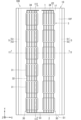
- FIG. 1 is a plan view showing an example of the external appearance of the solar cell module according to the first embodiment when viewed from above.
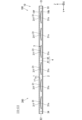
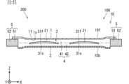
- FIG. 2 is a diagram illustrating an example of a virtual cross section of the solar cell module in FIG. 1 taken along line II-II.
- FIG. 3 is a diagram illustrating an example of a virtual cross section of the solar cell module in FIG. 1 taken along line III-III.
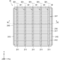
- FIG. 4 is a diagram illustrating an example of the structure of the solar cell element when viewed from above on the first element surface.
- FIG. 5 is a diagram illustrating an example of a structure when the second element surface of the solar cell element is viewed from above.
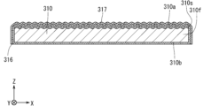
- FIG. 6 is a diagram illustrating an example of a virtual cross section of the solar cell element of FIGS.
- FIG. 7 is a diagram showing an example of a bent state of the solar cell module according to the first embodiment.
- FIG. 8 is a diagram illustrating an example of a state of a virtual cut surface during manufacturing in a specific example of a method for manufacturing a solar cell element.
- FIG. 9 is a diagram illustrating an example of a state of a virtual cut surface during manufacturing in a specific example of a method for manufacturing a solar cell element.
- FIG. 10 is a diagram illustrating an example of a state of a virtual cut surface during manufacture in a specific example of a method for manufacturing a solar cell element.
- FIG. 11 is a diagram illustrating an example of a state of a virtual cut surface during manufacture in a specific example of a method for manufacturing a solar cell element.
- FIG. 12 is a diagram illustrating an example of a state of a virtual cut surface during manufacturing in a specific example of a method for manufacturing a solar cell element.
- FIG. 13 is a diagram illustrating an example of the state of a virtual cut surface during manufacture in a specific example of the method for manufacturing a solar cell module according to the first embodiment.
- FIG. 14 is a diagram illustrating an example of the state of a virtual cut surface during manufacture in a specific example of the method for manufacturing a solar cell module according to the first embodiment.
- FIG. 12 is a diagram illustrating an example of a state of a virtual cut surface during manufacturing in a specific example of a method for manufacturing a solar cell element.
- FIG. 13 is a diagram illustrating an example of the state of a virtual cut surface during manufacture in a specific example of the method for manufacturing a solar cell module according
- FIG. 15 is a diagram showing an example of a virtual cut surface at a position corresponding to the virtual cut surface in FIG. 2 of the solar cell module according to the second embodiment.
- FIG. 16 is a diagram illustrating an example of a virtual cut plane at a position corresponding to the virtual cut plane in FIG. 3 of the solar cell module according to the second embodiment.
- FIG. 17 is a diagram illustrating an example of the state of a virtual cut surface during manufacture in a specific example of the method for manufacturing a solar cell module according to the second embodiment.
- FIG. 18 is a diagram illustrating an example of the state of a virtual cut surface during manufacture in a specific example of the method for manufacturing a solar cell module according to the second embodiment.
- FIG. 16 is a diagram illustrating an example of a virtual cut plane at a position corresponding to the virtual cut plane in FIG. 3 of the solar cell module according to the second embodiment.
- FIG. 17 is a diagram illustrating an example of the state of a virtual cut surface during manufacture in a specific example of the method
- FIG. 19 is a plan view showing an example of the external appearance of the solar cell module according to the third embodiment when viewed from above.
- FIG. 20 is a diagram illustrating an example of a virtual cut surface of the solar cell module of FIG. 19 along line XX-XX.
- FIG. 21 is a diagram illustrating an example of a virtual cut surface of the solar cell module of FIG. 19 along line XXI-XXI.
- FIG. 22 is a diagram schematically showing an example of a path through which rainwater flows on the first protective layer of the solar cell module according to the third embodiment.
- FIG. 23 is a diagram illustrating an example of the state of a virtual cut surface during manufacture in a specific example of the method for manufacturing a solar cell module according to the third embodiment.
- FIG. 20 is a diagram illustrating an example of a virtual cut surface of the solar cell module of FIG. 19 along line XX-XX.
- FIG. 21 is a diagram illustrating an example of a virtual cut surface of the solar cell module of FIG
- FIG. 24 is a diagram illustrating an example of the state of a virtual cut surface during manufacture in a specific example of the method for manufacturing a solar cell module according to the third embodiment.
- FIG. 25 is a diagram illustrating an example of a virtual cut plane at a position corresponding to the virtual cut plane in FIG. 20 of the solar cell module according to the fourth embodiment.
- FIG. 26 is a diagram showing an example of a virtual cut surface at a position corresponding to the virtual cut surface in FIG. 21 of the solar cell module according to the fourth embodiment.
- FIG. 27 is a diagram illustrating an example of the state of a virtual cut surface during manufacture in a specific example of the method for manufacturing a solar cell module according to the fourth embodiment.
- FIG. 28 is a diagram illustrating an example of the state of a virtual cut surface during manufacture in a specific example of the method for manufacturing a solar cell module according to the fourth embodiment.
- FIG. 29 is a diagram showing an example of a virtual cut surface at a position corresponding to the virtual cut surface in FIG. 21 of the solar cell module according to another embodiment.
- FIG. 30 is a diagram showing an example of a virtual cut surface at a position corresponding to the virtual cut surface in FIG. 21 of the solar cell module according to another embodiment.
- FIG. 31 is a diagram schematically showing an example of a path through which rainwater flows on the first protective layer of a solar cell module according to another embodiment.
- FIG. 32 is a diagram showing an example of a virtual cut surface at a position corresponding to the virtual cut surface in FIG.
- FIG. 33 is a plan view showing an example of the external appearance of a solar cell module according to another embodiment when viewed from above.
- FIG. 34 is a plan view showing an example of the external appearance of a solar cell module according to another embodiment when viewed from above.
- a solar cell module in which a plurality of solar cell elements are located between a protective layer on the front side and a protective layer on the back side.
- a plurality of solar cell elements are arranged in a plane and electrically connected to each other. Further, the plurality of solar cell elements are covered with a filler containing ethylene vinyl acetate copolymer (EVA) as a main component between the protective layer on the front side and the protective layer on the back side.
- EVA ethylene vinyl acetate copolymer
- FIGS. 1 to 34 A right-handed XYZ coordinate system is shown in FIGS. 1 to 34.
- the longitudinal direction of the front surface 10f of the solar cell panel 10 is set as the ⁇ Y direction as the first direction.
- the lateral direction of the front surface 10f of the solar cell panel 10 is the +X direction as the second direction.
- the direction opposite to the +Z direction is the third direction, which is the -Z direction.
- the direction opposite to the +X direction as the second direction is the -X direction as the fourth direction.
- the direction opposite to the -Y direction as the first direction is the +Y direction as the fifth direction.
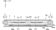
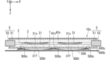
- the solar cell module 100 includes, for example, a solar cell panel 10.
- the solar cell panel 10 has, for example, a light-receiving surface (also referred to as a front surface) 10f through which light mainly enters, and a back surface 10b located on the opposite side of the front surface 10f.
- the front surface 10f is in a state facing the +Z direction.
- the back surface 10b is in a state facing the -Z direction.
- the +Z direction is set, for example, in a direction facing the sun, which is in the south.
- the front surface 10f has a rectangular shape.
- Solar cell module 100 may further include a terminal box (not shown) for extracting the power generated by solar cell panel 10 to the outside.
- the solar cell panel 10 includes, for example, a first protective layer 1, a second protective layer 2, a solar cell part 3, a filler 4, and a support member 5.
- a first protective layer 1 As shown in FIGS. 1 to 3, the solar cell panel 10 includes, for example, a first protective layer 1, a second protective layer 2, a solar cell part 3, a filler 4, and a support member 5.
- a second protective layer 2 As shown in FIGS. 1 to 3, the solar cell panel 10 includes, for example, a first protective layer 1, a second protective layer 2, a solar cell part 3, a filler 4, and a support member 5.
- a support member 5 we are prepared.
- the first protective layer 1 has, for example, a first surface 1f and a second surface 1s.
- the first surface 1f constitutes, for example, the front surface 10f of the solar cell panel 10. That is, the first protective layer 1 has a rectangular shape.
- the first surface 1f is exposed to a space (also referred to as external space) 200 outside the solar cell module 100.
- the second surface 1s is a surface of the first protective layer 1 that is opposite to the first surface 1f.
- the first protective layer 1 has, for example, light-transmitting properties. Specifically, the first protective layer 1 has, for example, transparency to light having a wavelength in a specific range.
- the specific range of wavelengths includes, for example, the wavelength of light that can be photoelectrically converted by the solar cell unit 3. If the wavelengths in the specific range include wavelengths of sunlight with high irradiation intensity, the photoelectric conversion efficiency of the solar cell module 100 can be improved.
- the first protective layer 1 As the material of the first protective layer 1, for example, a translucent resin is applied.
- the first protective layer 1 is made of a translucent resin.
- This light-transmitting resin may have weather resistance.
- weather resistance refers to a property that does not easily cause alterations such as deformation, discoloration, and deterioration when used outdoors, for example.
- the light-transmitting resin applied to the material of the first protective layer 1 may have flexibility.
- flexibility means, for example, soft and supple properties.
- the first protective layer 1 may be composed of, for example, one layer of resin.
- the first protective layer 1 has, for example, moisture permeable and waterproof properties.
- Moisture-permeable and waterproof properties for example, reduce the infiltration of water such as water droplets from the external space 200 of the solar cell module 100 toward the solar cell section 3, and also facilitate the passage of moisture from the filler 4 toward the external space 200.
- the resin having translucency and weather resistance includes, for example, a fluorine-based resin.
- Fluorine-based resins include, for example, fluorinated ethylene propylene copolymer (FEP), ethylene tetrafluoroethylene copolymer (ETFE), and ethylene chlorotrifluoroethylene copolymer (Ethylene Chlorotrifluoroethylene). :ECTFE) etc.
- the first protective layer 1 may be composed of two or more layers of resin.
- the fluorine-based resin applied to the first protective layer 1 may be, for example, two or more types of resin. Therefore, for example, a mode is conceivable in which the fluororesin applied to the first protective layer 1 includes one or more resins among FEP, ETFE, and ECTFE.
- the thickness of the first protective layer 1 is, for example, about 0.05 millimeter (mm) to 0.5 mm.
- the first protective layer 1 may be made of a moisture-permeable resin with a relatively low density. Moreover, the thickness of the first protective layer 1 may be thin. In this case, the first protective layer 1 is light. Therefore, the solar cell module 100 can be made lighter and thinner than, for example, a structure in which a high-density glass having a thickness of about 1 mm or more is used instead of the first protective layer 1.
- the material of the first protective layer 1 a resin different from the fluorine-based resin may be used instead of the fluorine-based resin, or together with the fluorine-based resin.
- a resin different from the fluorine-based resin for example, acrylic resin or polycarbonate is used as the resin different from the fluorine-based resin.
- the thickness of the resin is, for example, about 0.03 mm to 0.6 mm.
- the first protective layer 1 may have a structure in which a plurality of types of resins are laminated.
- the solar cell section 3 is located, for example, between the first protective layer 1 and the second protective layer 2. In other words, the solar cell section 3 is in a state of facing the first protective layer 1 and also facing the second protective layer 2 in the Z direction.
- the solar cell section 3 includes, for example, a plurality of solar cell elements 31.
- the plurality of solar cell elements 31 are located between the second surface 1s of the first protective layer 1 and the second protective layer 2. From another perspective, the plurality of solar cell elements 31 are located facing the second surface 1s of the first protective layer 1. Moreover, the plurality of solar cell elements 31 are lined up along the second surface 1s of the first protective layer 1. In other words, the plurality of solar cell elements 31 are arranged in a plane along the second surface 1s of the first protective layer 1. In the examples shown in FIGS. 1 to 3, the plurality of solar cell elements 31 are two-dimensionally lined up.
- the solar cell section 3 further includes, for example, a plurality of first wiring members 32, a second wiring member 33, and a third wiring member 34.
- the solar cell section 3 includes, for example, a plurality of solar cell strings 30.
- the solar cell section 3 includes two solar cell strings 30 as the plurality of solar cell strings 30.
- the plurality of solar cell strings 30 are lined up in the X direction.
- Each of the plurality of solar cell strings 30 includes, for example, two or more solar cell elements 31 and a plurality of first wiring members 32.
- each solar cell string 30 in each solar cell string 30, two or more solar cell elements 31 are lined up in, for example, the ⁇ Y direction as the first direction.
- each solar cell string 30 includes six solar cell elements 31 as the two or more solar cell elements 31.
- each solar cell string 30 may include two solar cell elements 31 as the two or more solar cell elements 31, or may include an arbitrary number of three or more solar cell elements 31. good.
- the plurality of solar cell elements 31 include two solar cell elements 31 lined up in the ⁇ Y direction as the first direction.
- the plurality of first wiring members 32 are in a state of electrically connecting two mutually adjacent solar cell elements 31 among the two or more solar cell elements 31.
- the second wiring member 33 is in a state of electrically connecting two adjacent solar cell strings 30 of the two or more solar cell strings 30 .
- One third wiring member 34 is connected to each of the two solar cell strings 30.
- the solar cell section 3 is connected to the third wiring member 34 connected to the solar cell string 30 located at the end in the -X direction and the third wiring member 34 located at the end in the +X direction. and a third wiring member 34 connected to the solar cell string 30 that is connected to the solar cell string 30.
- Each of the two third wiring members 34 has a portion drawn out to the outside of the solar cell panel 10.
- Each of the plurality of solar cell elements 31 can convert light energy into electrical energy.
- Each of the plurality of solar cell elements 31 has, for example, a plate-like shape.
- Each of the plurality of solar cell elements 31 has a first element surface 31f and a second element surface 31s.
- the first element surface 31f is a surface facing the second surface 1s of the first protective layer 1.
- the second element surface 31s is a surface of the solar cell element 31 on the opposite side to the first element surface 31f. In other words, the second element surface 31s faces the second protective layer 2.
- the first element surface 31f is in a state facing the +Z direction
- the second element surface 31s is in a state facing the ⁇ Z direction.
- the first element surface 31f primarily serves as a surface on which light is incident (also referred to as a light-receiving surface), and the second element surface 31s primarily serves as a surface on which light is not incident (non-light-receiving surface). It has a role as a surface (also called a surface).
- Each of the first element surface 31f and the second element surface 31s has a rectangular shape such as a substantially square shape, for example.
- Each of the first element surface 31f and the second element surface 31s may have a shape in which corners are cut.
- Each of the first element surface 31f and the second element surface 31s has, for example, a substantially square shape with a side length of about 100 mm to 250 mm.
- Each of the first element surface 31f and the second element surface 31s may have a substantially rectangular shape, for example.
- each of the plurality of solar cell elements 31 includes a semiconductor substrate 310, a first electrode 311, a second electrode 312, a third electrode 313, a fourth electrode 314.
- the semiconductor substrate 310 includes, for example, a crystalline semiconductor such as crystalline silicon, an amorphous semiconductor such as amorphous silicon, four types of elements such as copper, indium, gallium, and selenium, or two types of elements such as cadmium and tellurium. Compound semiconductors using Here, it is assumed that crystalline silicon is applied to the semiconductor substrate 310.
- the semiconductor substrate 310 mainly includes a semiconductor region 310f having a first conductivity type (also referred to as a first conductivity type region) and a second conductivity type region 310f opposite to the first conductivity type. It has a semiconductor region (also referred to as a second conductivity type region) 310s having a conductivity type.
- the first conductivity type region 310f is located, for example, on the second element surface 31s side of the semiconductor substrate 310 in the ⁇ Z direction.
- the second conductivity type region 310s is located, for example, in a surface layer portion of the semiconductor substrate 310 on the first element surface 31f side in the +Z direction.
- the semiconductor substrate 310 has a pn junction located at the interface between the first conductivity type region 310f and the second conductivity type region 310s.
- the thickness of the semiconductor substrate 310 is, for example, about 0.15 mm to 0.5 mm.
- each solar cell element 31 has a plurality of first electrodes 311 and a plurality of second electrodes 312.
- a plurality of substantially parallel first electrodes 311 and a large number of substantially parallel second electrodes 312 are located on the first element surface 31f side of the semiconductor substrate 310.
- first electrodes 311 as a plurality of substantially parallel first electrodes 311 and a large number of second electrodes 312 as a plurality of substantially parallel second electrodes 312 are substantially perpendicular to each other. It is located in a state of being.
- each of the plurality of first electrodes 311 has a long shape elongated in the -Y direction as the first direction
- each of the plurality of second electrodes 312 has a long shape in the -Y direction as the first direction. It has a linear shape that is long in the +X direction.
- each solar cell element 31 has a fifth electrode 315 located along the outer edge in the -X direction and a fifth electrode 315 located along the outer edge in the +X direction on the first element surface 31f side, for example. and a fifth electrode 315 located along the line.
- Each fifth electrode 315 interconnects, for example, a large number of substantially parallel second electrodes 312 .
- an antireflection film 317 may be located on the second conductivity type region 310s of the semiconductor substrate 310 in a region where the first electrode 311 and the second electrode 312 are not formed.
- an insulating film made of silicon nitride or the like is applied to the antireflection film 317.
- a passivation film 316 may be present between the second conductivity type region 310s of the semiconductor substrate 310 and the antireflection film 317.
- a thin film made of an oxide such as aluminum oxide or a nitride is applied to the passivation film 316.
- the main component of the first electrode 311 when the main component of the first electrode 311 is silver, the silver paste is applied in a desired shape by a screen printing method or the like, and then the silver paste is fired, thereby forming the first electrode 311. 311 may be formed.
- the term "main component” refers to a component that has the largest (highest) ratio (also referred to as content rate) of the components constituting a substance.
- a metal paste containing a metal powder containing silver as a main component, an organic vehicle, and a glass frit is applied to the silver paste.
- the main component of the second electrode 312 when the main component of the second electrode 312 is silver, the second electrode 312 is formed by applying a silver paste into a desired shape using a screen printing method or the like and then firing the silver paste.
- the fifth electrode 315 is formed by applying a silver paste into a desired shape using a screen printing method or the like, and then firing the silver paste. can be done.
- the first electrode 311, the second electrode 312, and the fifth electrode 315 may be formed in separate steps, or may be formed in the same step.
- the third electrode 313 and the fourth electrode 314 are located on the second element surface 31s side of the semiconductor substrate 310, for example.
- a busbar electrode is applied to the third electrode 313.
- a plurality of substantially parallel third electrodes 313 are located on the second element surface 31s side of the semiconductor substrate 310. More specifically, five rows of third electrodes 313 that are substantially parallel to each other are located on the second element surface 31s side of the semiconductor substrate 310.
- Each of the five rows of third electrodes 313 is located along the -Y direction, which is the first direction. More specifically, each of the five rows of third electrodes 313 includes, for example, a plurality of electrode parts lined up in a row.
- the plurality of electrode parts is composed of, for example, six electrode parts.
- the fourth electrode 314 is located on the second element surface 31s side of the semiconductor substrate 310, except for a portion where the third electrode 313 and the fourth electrode 314 overlap and are connected to each other. It is located on almost the entire surface of the area where it is not located. Note that the fourth electrode 314 does not need to be located on substantially the entire surface, and may be located in a grid pattern, for example.
- a passivation film 316 may be present between the first conductivity type region 310f of the semiconductor substrate 310 and the third electrode 313 and the fourth electrode 314. .
- a thin film made of an oxide such as aluminum oxide or a nitride is applied to the passivation film 316.
- the passivation film 316 has a desired pattern between the first conductivity type region 310f and the third electrode 313 and the fourth electrode 314.
- a film (also referred to as a protective film) 318 for protecting the passivation film 316 may be present between the passivation film 316 and the fourth electrode 314.
- the protective film 318 For example, a thin film made of an oxide such as silicon oxide is used as the protective film 318.
- the protective film 318 has a desired pattern between the passivation film 316 and the fourth electrode 314.
- the protective film 318 does not need to be present between the passivation film 316 and the third electrode 313 as shown in FIG.
- the protective film 318 has a plurality of holes in which the third electrode 313 is located.
- the protective film 318 may be present between the passivation film 316 and the third electrode 313.
- the passivation film 316 and the protective film 318 have, for example, a large number of through holes for bringing a part of the fourth electrode 314 into contact with the first conductivity type region 310f.
- the first conductivity type region 310f is a region in which the concentration of a dopant element of the first conductivity type is higher than other regions of the first conductivity type region 310f (also referred to as a high concentration region) in a portion of the surface layer that is in contact with the fourth electrode 314. It has a BSF (Back Surface Field) area) of 310t.
- the main component of the third electrode 313 is silver
- the silver paste is applied in a desired shape by a screen printing method or the like, and then the silver paste is fired, thereby forming the third electrode 313.
- 313 may be formed.
- the main component of the fourth electrode 314 is aluminum
- the fourth electrode 314 is formed by applying aluminum paste into a desired shape using a screen printing method or the like, and then firing the aluminum paste. can be done.
- a metal paste containing a metal powder containing aluminum as a main component, an organic vehicle, and a glass frit is applied to the aluminum paste.
- the first wiring material 32 electrically connects, for example, the first electrode 311 of one solar cell element 31 and the third electrode 313 of another solar cell element 31 adjacent to this one solar cell element 31. It is in a connected state.
- the outer edges of the plurality of first wiring members 32 attached to each of the solar cell elements 31 are virtually drawn with thin two-dot chain lines.
- the first wiring member 32 has an elongated shape that is elongated in the ⁇ Y direction as the first direction.
- the first wiring material 32 is in a state of being joined to the first electrode 311 and the third electrode 313, for example.
- first wiring material 32 and the first electrode 311 there is a part (also referred to as a first joint part) 321 where the first wiring material 32 and the first electrode 311 are joined. exists. Therefore, for example, the first wiring material 32 is in a state of being bonded to the first electrode 311 of one solar cell element 31 via the first bonding portion 321. Further, for example, between the first wiring material 32 and the third electrode 313, there is a part 322 that joins the first wiring material 32 and the third electrode 313 (also referred to as a second joint part). There is. Therefore, for example, the first wiring material 32 is in a state of being joined to the third electrode 313 of another solar cell element 31 adjacent to one solar cell element 31 via the second joint portion 322. .
- the material for the first joint portion 321 and the second joint portion 322 may be, for example, a low melting point alloy such as solder or a low melting point single metal. More specifically, for example, a copper foil having a thickness of about 0.1 mm to 0.2 mm and a width of about 1 mm to 2 mm is applied to the first wiring material 32. In this case, the entire surface of the first wiring material 32 may be coated with solder.
- the first wiring material 32 is in a state of being electrically connected to the first electrode 311 and the third electrode 313, for example, by soldering.
- the solder located between the first wiring material 32 and the first electrode 311 constitutes the first joint portion 321.
- the solder located between the first wiring material 32 and the third electrode 313 constitutes the second joint portion 322 .
- the filler 4 is in contact with the second surface 1s. Further, the filler 4 is positioned so as to cover the plurality of solar cell elements 31. In the first embodiment, the filler 4 is in a state covering the plurality of solar cell elements 31 between the first protective layer 1 and the second protective layer 2. In other words, the filler 4 covers the solar cell part 3 in the area between the first protective layer 1 and the second protective layer 2 (also referred to as the gap area), and is filled in this gap area. It is in. From another perspective, the filler 4 has a surface on the first protective layer 1 side that is in contact with the second surface 1s of the first protective layer 1 and a surface that is in contact with the second protective layer 2. It has a certain second protective layer 2 side surface.
- the filler 4 includes, for example, a filler (also referred to as a first filler) 41 located on the front surface 10f side and a filler (also referred to as a second filler) 42 located on the back surface 10b side.
- a filler 41 is in a state of covering the entire surface of the solar cell section 3 on the first protective layer 1 side.
- the first filler 41 is in a state of covering the plurality of solar cell elements 31, for example, between the first protective layer 1 and the plurality of solar cell elements 31.
- the second filler 42 is in a state, for example, covering the entire surface of the solar cell section 3 on the second protective layer 2 side.
- the second filler 42 is in a state of covering the plurality of solar cell elements 31, for example, between the second protective layer 2 and the plurality of solar cell elements 31. Therefore, in the first embodiment, the solar cell section 3 is sandwiched and surrounded by, for example, the first filler 41 and the second filler 42 . Thereby, for example, the attitude of the solar cell section 3 can be maintained by the filler 4.
- the filler 4 has, for example, translucency.
- the filler 4 has, for example, translucency to light having a wavelength in the above-mentioned specific range. For example, if at least the first filler 41 out of the first filler 41 and the second filler 42 constituting the filler 4 has translucency, the incident light from the front surface 10f side It can reach up to the solar cell section 3.
- the material of the first filler 41 for example, polyvinyl acetal such as ethylene-vinyl acetate copolymer (EVA), polyvinyl butyral (PVB), or acid-modified resin is used.
- EVA ethylene-vinyl acetate copolymer
- PVB polyvinyl butyral
- acid-modified resin includes, for example, a modified polyolefin resin that can be formed by graft modification of a resin such as polyolefin with an acid.
- acids that can be used for graft modification of acid-modified resins include acrylic acid, methacrylic acid, maleic acid, fumaric acid, itaconic acid, maleic anhydride, hymic anhydride, itaconic anhydride, and citraconic anhydride.
- Ru As the material for the second filler 42, for example, like the first filler 41, polyvinyl acetal such as EVA and PVB, acid-modified resin, etc. are used.
- Each of the first filler 41 and the second filler 42 may be made of two or more types of materials, for example.
- the second filler 42 may contain, for example, a pigment.
- a pigment for example, if the second filler 42 contains a white pigment, the light that has passed through the solar cell section 3 can be reflected by the second filler 42 and made to enter the solar cell section 3 again. . Thereby, the power generation efficiency of the solar cell module 100 can be improved.
- the filler 4 may not include the second filler 42 but may include the first filler 41.
- the first filler 41 is in a state covering the solar cell section 3 between the first protective layer 1 and the second protective layer 2.
- the first filler 41 is in a state covering the plurality of solar cell elements 31 between the first protective layer 1 and the second protective layer 2.
- the thickness of the filler 4 may be smaller in the portion covering the solar cell portion 3 and greater in the portion between the solar cell portion 3 and the support member 5.
- the maximum value of the thickness of the filler 4 between the solar cell section 3 and the support member 5 is the same as that between two adjacent solar cell elements 31 among the plurality of solar cell elements 31. It is larger than the maximum thickness of the filler 4.
- the distance between the first protective layer 1 and the second protective layer 2 is small in the area where the solar cell part 3 is sandwiched, and the distance between the first protective layer 1 and the second protective layer 2 is small in the area where the solar cell part 3 and the support member 5 are sandwiched. It may be large in the part where it is.
- the maximum value of the distance between the first protective layer 1 and the second protective layer 2 in the area sandwiching the area between the solar cell part 3 and the support member 5 is the part where the solar cell part 3 is sandwiched. It may be larger than the maximum value of the distance between the first protective layer 1 and the second protective layer 2 in .
- the thickness of the filler 4 increases as it goes from the solar cell section 3 toward the support member 5. Gradually increasing portions may also be present. In other words, for example, in at least a part of the region between the support member 5 and the solar cell section 3, the thickness of the filler 4 monotonically increases from the solar cell section 3 toward the support member 5. may exist.
- the filler 4 has a shape that is line symmetrical to each other with respect to the XY plane, but the drawing is only schematically shown and is not necessarily limited to this.
- the second protective layer 2 is in a state of forming the back surface 10b of the solar cell panel 10, for example.
- the second protective layer 2 is in contact with, for example, the surface of the filler 4 on the side opposite to the first protective layer 1 .
- the second protective layer 2 is in contact with the filler 4 on the opposite side of the filler 4 from the first protective layer 1 .
- the second protective layer 2 is in contact with the filler 4 at a surface of the filler 4 that is opposite to the surface of the filler 4 that is in contact with the first protective layer 1 .
- the second protective layer 2 is located facing the solar cell section 3 and the first portion 51 of the support member 5 in the Z direction.
- the first portion 51 is a portion of the support member 5 that is located closer to the solar cell unit 3 than the second portion 52 in the X direction.
- the second protective layer 2 can, for example, protect the solar cell section 3 from the back surface 10b side.
- a back sheet forming the back surface 10b is applied to the second protective layer 2.
- the thickness of the back sheet is, for example, about 0.15 mm to 0.5 mm.
- resin is used as the material for the back sheet.
- the same material as the first protective layer 1 can be applied to this resin.
- the second protective layer 2 has the same or substantially the same shape as the first protective layer 1 when viewed from the rear surface 10b side. For example, a configuration is adopted in which both the first protective layer 1 and the second protective layer 2 have a rectangular outer shape when viewed from the rear surface 10b side.
- the support member 5 is a member for improving the rigidity of the solar cell panel 10.
- the support member 5 has higher rigidity than all of the first protective layer 1, second protective layer 2, and filler 4.
- the support member 5 is, for example, a rigid body having high rigidity.
- metal may be used as the material of the support member 5. This metal may be, for example, aluminum or stainless steel.
- the support member 5 is located adjacent to the solar cell section 3 with a space therebetween. More specifically, the support member 5 is located adjacent to the solar cell section 3 with a space therebetween in a plan view.
- Support member 5 includes a first portion 51 and a second portion 52.
- Planar view means a planar view of each part as viewed in the ⁇ Z direction as the third direction, unless specific conditions are stated. From another point of view, when viewed from above toward the first surface 1f of the first protective layer 1, the support member 5 is adjacent to the solar cell section 3 with an interval in the +X direction as the second direction. It is located in a state of being.
- the first portion 51 is located between the first protective layer 1 and the second protective layer 2 and covered with the filler 4. In other words, the first portion 51 is located facing the second surface 1s of the first protective layer 1. Further, the first portion 51 is located facing the second protective layer 2 . In the example of FIG. 2, the first portion 51 is in a state facing the second surface 1s of the first protective layer 1 in the Z direction. The first portion 51 also faces the second protective layer 2 in the Z direction.
- the filler 4 includes a portion located between the second surface 1s of the first protective layer 1 and the first portion 51. More specifically, the first filler 41 includes a portion located between the second surface 1s of the first protective layer 1 and the first portion 51 in the ⁇ Z direction as the third direction. Further, the filler 4 includes a portion located between the second protective layer 2 and the first portion 51. More specifically, the second filler 42 includes a portion located between the first portion 51 and the second protective layer 2 in the -Z direction as the third direction.
- the second portion 52 is a portion of the support member 5 located on the opposite side to the solar cell section 3 side.
- the support member 5 includes a first portion 51 located on the solar cell section 3 side, and a second portion 52 located on the opposite side of the solar cell section 3 with respect to the first section 51. ,including.
- the second portion 52 may be considered to be a portion of the support member 5 other than the first portion 51 .
- the second portion 52 is in a state of protruding from the first portion 51 from the filler 4 covering the first portion 51 in a direction opposite to the solar cell portion 3 . More specifically, the second portion 52 is located on the opposite side (also referred to as the outside) of the solar cell section 3 with respect to the first portion 51 in plan view.
- the second portion 52 is located not facing the second surface 1s of the first protective layer 1, and is not covered with the filler 4.
- the second portion 52 is in a state of protruding from the first portion 51 to the outside of the first protective layer 1 and the second protective layer 2 in plan view.
- the second portion 52 is not facing the first protective layer 1 in the Z direction.
- the second portion 52 is in a state where it does not also face the second protective layer 2 in the Z direction.
- the first portion 51 is located on the solar cell section 3 side (also referred to as inside) with respect to the second portion 52 in plan view.
- the support member 5 has a plate-like shape. More specifically, the support member 5 has a rectangular shape in plan view. In the example of FIG. 2, the XZ cross section of the support member 5 also has a rectangular shape. The corners of the support member 5 may be chamfered as appropriate.
- the longitudinal direction of the support member 5 is located along one side of the first protective layer 1, for example.
- the longitudinal direction of the support member 5 is the Y direction.
- the longitudinal direction of the support member 5 is located, for example, along the direction in which two or more solar cell elements 31 are arranged in one solar cell string 30 (also referred to as the arrangement direction).
- the arrangement direction of the plurality of solar cell elements 31 in one solar cell string 30 is the Y direction.
- the longitudinal direction of the support member 5 is located along the longitudinal direction of the first wiring member 32, for example.
- the longitudinal direction of the first wiring member 32 is the Y direction.
- the solar cell panel 10 includes two support members 5.
- the two support members 5 include a first support member 5 and a second support member 5.
- the first support member 5 is located at the end of the solar cell panel 10 in the ⁇ X direction, which is the fourth direction.
- the second support member 5 is located at the end of the solar cell panel 10 in the +X direction as the second direction.
- the second portion 52 is located on the side of the first portion 51 in the ⁇ X direction, which is the fourth direction.
- the second portion 52 is located on the side of the first portion 51 in the +X direction as the second direction.
- the first support member 5 is located along the first side of the first protective layer 1.
- the first side is one side of the first protective layer 1 located at the end in the ⁇ X direction as the fourth direction.
- the second support member 5 is located along the second side of the first protective layer 1 .
- the second side is one side of the first protective layer 1 located at the end in the +X direction as the second direction.
- each of the first side and the second side is located extending along the Y direction.
- Each of the two support members 5 has a rectangular front and back surface whose longitudinal direction is the Y direction and whose transversal direction is the X direction.
- the length of each support member 5 in the longitudinal direction is, for example, the same or approximately the same as the length of the first protective layer 1.
- each support member 5 in the lateral direction is set to, for example, several tens of mm or more.
- the length (width) of the first portion 51 in the transverse direction is set to, for example, about 20% to 80% of the width of the support member 5.
- the thickness of each support member 5 is larger than the thickness of the solar cell section 3, for example.
- the thickness of each support member 5 is set, for example, to about 1 mm to 5 mm.
- the second portion 52 of the support member 5 is attached, for example, to a portion to which a building material or the like is to be attached (also referred to as an attachment target portion).
- the second portion 52 may have a mounting hole (not shown).
- This attachment hole is a hole (also referred to as a through hole) that penetrates the second portion 52 in the Z direction.
- a mounting part also referred to as a mounting part
- the solar panel 10 can be attached to the attachment target part.
- the support members 5 are located at each end of the solar cell panel 10 in the -X direction as the fourth direction and the end in the +X direction as the second direction. Therefore, the two support members 5 located at both ends of the solar cell panel 10 in the X direction can be fixed to the attachment target part. Thereby, the solar cell panel 10 can be firmly attached to the attachment target part. Therefore, the support member 5 has a role as a member (also referred to as an attachment member) for attaching the solar cell panel 10 to an object to be attached. Therefore, by providing the support member 5, the solar cell module 100 can easily and stably fix the solar cell module 100 to the attachment target part.
- the support members 5 are not mainly located on both sides of the solar cell panel 10 in the Y direction. More specifically, the support member 5 supports each of the -Y direction end (also referred to as a first end) E1 and the +Y direction end (also referred to as a second end) E2 of the solar cell panel 10. is not actually located.
- the first end E1 and the second end E2 are ends along the X direction. Therefore, as shown in FIG. 7, by applying the external force F1 to the support member 5, the solar cell panel 10 can be bent in an arc shape when viewed in the direction along the +Y direction.
- the solar cell panel 10 can bend to a state along an arc with a radius of about several hundred mm.
- a case can be considered in which a circular arc of approximately several hundred mm is a circular arc of approximately 500 mm. Thereby, the solar cell panel 10 can be easily attached to the curved attachment target part.
- a configuration is adopted in which one of the YZ cross section and the XZ cross section of the solar cell element 31 is curved in a convex shape protruding toward the second surface 1s.
- the YZ cross section of the solar cell element 31 is a virtual cross section along each of the -Y direction as the first direction and the -Z direction as the third direction of the solar cell element 31.
- the XZ cross section of the solar cell element 31 is a virtual cross section along each of the +X direction as the second direction and the -Z direction as the third direction of the solar cell element 31.
- the XZ cross section of the first element surface 31f is curved in a convex shape protruding toward the second surface 1s, and the XZ cross section of the second element surface 31s is curved toward the second surface 1s.
- a curved shape that is concave in the direction toward the surface 1s is adopted.
- the XZ cross section of the first element surface 31f is a virtual cross section along the +X direction as the second direction and the ⁇ Z direction as the third direction with respect to the first element surface 31f.
- the XZ cross section of the second element surface 31s is a virtual cross section along the +X direction as the second direction and the ⁇ Z direction as the third direction with respect to the second element surface 31s.
- the first element surface 31f is curved in a convex shape along the first virtual arc surface.
- the first virtual arc surface is a circular arc that is curved in a convex shape protruding toward the +Z direction, which is opposite to the -Z direction as the third direction, in the -Y direction as the first direction on the XZ plane. It is a virtual curved surface formed by The XZ plane is a virtual plane along the +X direction as the second direction and the -Z direction as the third direction.
- the second element surface 31s is curved concavely along the second virtual arc surface.
- the second virtual arc surface is a circular arc that is curved in a convex shape protruding toward the +Z direction, which is opposite to the -Z direction as the third direction, in the -Y direction as the first direction on the XZ plane. It is a virtual curved surface formed by For example, the second virtual arc surface is located along the first virtual arc surface.
- the YZ cross section of the first element surface 31f is curved in a convex shape protruding toward the second surface 1s
- the YZ cross section of the second element surface 31s is curved toward the second surface 1s.
- a curved shape that is concave in the direction toward the surface 1s may be adopted.
- the first element surface 31f is curved in a convex shape along the third virtual arc surface.
- the third virtual arc surface is a circular arc that is curved in a convex shape protruding toward the +Z direction, which is opposite to the -Z direction as the third direction, in the YZ plane, and extends in the +X direction as the second direction.
- the YZ plane is a virtual plane along each of the -Y direction as the first direction and the -Z direction as the third direction.
- the second element surface 31s is curved concavely along the fourth virtual arc surface.
- the fourth virtual arc surface is a circular arc that is curved in a convex shape protruding toward the +Z direction, which is opposite to the -Z direction as the third direction, in the +X direction as the second direction on the YZ plane. It is a virtual curved surface formed by For example, the fourth virtual arc surface is located along the third virtual arc surface.
- the solar cell element 31 may be curved along a virtual spherical surface.
- the first element surface 31f may have a convexly curved shape along a part of the first virtual spherical surface
- the second element surface 31s may have a shape that is curved in a convex manner along a part of the first virtual spherical surface. , it may have a shape that is concavely curved along a part of the second virtual spherical surface.
- the second virtual spherical surface is located along the first virtual spherical surface.
- the radius of each of the first virtual spherical surface and the second virtual spherical surface is set, for example, to approximately several hundred mm to several thousand mm.
- the first protective layer 1 is made of a transparent resin. Therefore, for example, by making the first protective layer 1 thinner, the weight of the solar cell module 100 can be reduced.
- the first element surface 31f facing the second surface 1s of the first protective layer 1 has a convex shape. It is curved to. Further, for example, in each of the plurality of solar cell elements 31 of the solar cell section 3, the second element surface 31s on the opposite side to the first element surface 31f is curved in a concave shape. From another point of view, the plate-shaped solar cell element 31 has a curved convex shape protruding toward the second surface 1s of the first protective layer 1.
- the solar cell element 31 is curved in a convex shape protruding toward the first protective layer 1, various objects such as falling objects and flying objects collide with the first protective layer 1.
- the impact on the solar cell element 31 can be alleviated.
- the solar cell element 31 becomes difficult to break.
- the impact resistance of the solar cell element 31 can be improved.
- the power generation efficiency of the solar cell module 100 is less likely to decrease. Therefore, for example, it is possible to achieve both weight reduction and improvement in power generation efficiency in the solar cell module 100. That is, it is possible to reduce the weight of the solar cell module 100 and improve the power generation efficiency.
- the solar cell element 31 is curved in a convex shape protruding toward the first protective layer 1, the impact resistance of the solar cell element 31 can be improved. Therefore, by making the first protective layer 1 thinner, it is possible to reduce the weight of the solar cell module 100. As a result, for example, it is possible to achieve both weight reduction and improvement in power generation efficiency in the solar cell module 100.
- a semiconductor substrate 310 is prepared.
- Semiconductor substrate 310 has a first surface 310a and a second surface 310b opposite to first surface 310a.
- the semiconductor substrate 310 may be formed using, for example, the existing Czochralski (CZ) method or casting method.
- CZ Czochralski
- an example using an ingot of p-type polycrystalline silicon as the first conductivity type produced by a casting method will be described.
- the semiconductor substrate 310 is manufactured by slicing this ingot to a desired thickness of, for example, 250 ⁇ m or less.
- etching the surface of the semiconductor substrate 310 in a small amount with an aqueous solution such as sodium hydroxide, potassium hydroxide, or fluoronitric acid
- an aqueous solution such as sodium hydroxide, potassium hydroxide, or fluoronitric acid
- Textured structures can be formed by wet or dry etching.
- Wet etching may be performed using, for example, an alkaline aqueous solution such as sodium hydroxide or an acidic aqueous solution such as fluoronitric acid.
- Dry etching may be performed using, for example, a reactive ion etching (RIE) method.
- RIE reactive ion etching
- a second conductivity type region 310s which is an n-type semiconductor region as a second conductivity type, is formed on a first surface 310a of the semiconductor substrate 310 having a textured structure. More specifically, a second conductivity type region 310s, which is a region of an n-type semiconductor as a second conductivity type, is formed in a surface layer portion of the semiconductor substrate 310 on the first surface 310a side having a textured structure.
- the second conductivity type region 310s may be formed using, for example, a coating thermal diffusion method or a vapor phase thermal diffusion method.
- the coating thermal diffusion method includes, for example, applying diphosphorus pentoxide (P 2 O 5 ) in the form of a paste onto the surface of the semiconductor substrate 310 to thermally diffuse phosphorus.
- the vapor phase thermal diffusion method uses, for example, gaseous phosphorus oxychloride (POCl 3 ) as a diffusion source.
- POCl 3 gaseous phosphorus oxychloride
- the second conductivity type region 310s formed on the second surface 310b side is treated with an aqueous solution of fluoronitric acid. Remove by etching.
- the phosphorus glass attached to the first surface 310a side of the semiconductor substrate 310 when forming the second conductivity type region 310s is removed by etching.
- a diffusion mask may be formed in advance on the second surface 310b side of the semiconductor substrate 310, the second conductivity type region 310s may be formed by a vapor phase thermal diffusion method, and then the diffusion mask may be removed. good.
- a passivation film 316 is formed at least on the second surface 310b of the semiconductor substrate 310.
- a passivation film 316 is formed on each of the second surface 310b and the first surface 310a of the semiconductor substrate 310.
- the passivation film 316 may be composed of, for example, a film mainly containing aluminum oxide.
- the passivation film 316 may be formed by, for example, an atomic layer deposition (ALD) method.
- ALD atomic layer deposition
- the passivation film 316 can be formed all around the semiconductor substrate 310 including the end surface.
- the step of forming the passivation film 316 by the ALD method first, the semiconductor substrate 310, on which the second conductivity type region 310s has been formed, is placed in a chamber of a film forming apparatus. Then, the following steps A to D are repeated multiple times while the semiconductor substrate 310 is heated to a temperature range of about 100 degrees Celsius (100 degrees Celsius) to 250 degrees Celsius (250 degrees Celsius), thereby removing aluminum oxide mainly.
- a passivation film 316 containing As a result, a passivation film 316 having a desired thickness is formed.
- Step A An aluminum raw material such as trimethylaluminum (TMA) for forming aluminum oxide is supplied onto the semiconductor substrate 310 together with a carrier gas such as Ar gas or nitrogen gas. As a result, the aluminum raw material is adsorbed all around the semiconductor substrate 310.
- the time for which TMA is supplied is set, for example, to about 15 milliseconds to 3000 milliseconds.
- the surface of the semiconductor substrate 310 is terminated with hydroxyl groups (OH groups).
- the surface of the semiconductor substrate 310 has a Si--O--H structure. This structure can be formed, for example, by treating the semiconductor substrate 310 with dilute hydrofluoric acid and cleaning with pure water in the order described.
- Step B The inside of the chamber of the film forming apparatus is cleaned using nitrogen gas.
- the aluminum raw material in the chamber is removed, and the aluminum raw materials other than the component chemically adsorbed at the atomic layer level among the aluminum raw materials physically adsorbed and chemically adsorbed on the semiconductor substrate 310 are removed.
- the time for purifying the inside of the chamber with nitrogen gas is set, for example, from about 1 second to several tens of seconds.
- Step C An oxidizing agent such as water or ozone gas is supplied into the chamber of the film forming apparatus. As a result, the alkyl group contained in TMA is removed and replaced with an OH group. As a result, an atomic layer of aluminum oxide is formed on the semiconductor substrate 310.
- the time for supplying the oxidizing agent into the chamber is set, for example, to about 750 milliseconds to 1100 milliseconds.
- hydrogen may be supplied into the chamber together with an oxidizing agent to cause the aluminum oxide to contain hydrogen atoms.
- Step D Purify the chamber of the film forming apparatus with nitrogen gas. This removes the oxidizing agent in the chamber.
- the oxidizing agent that did not contribute to the reaction during the formation of aluminum oxide at the atomic layer level on the semiconductor substrate 310 is removed.
- the time for purifying the inside of the chamber with nitrogen gas is set, for example, from about 1 second to several tens of seconds.
- an antireflection film 317 is formed on the passivation film 316.
- the antireflection film 317 may be made of, for example, a silicon nitride film.
- the antireflection film 317 may be formed using, for example, a plasma-enhanced chemical vapor deposition (PECVD) method or a sputtering method.
- PECVD plasma-enhanced chemical vapor deposition
- the semiconductor substrate 310 is heated in advance to a temperature higher than the temperature during the formation of the antireflection film 317.
- the reaction pressure is set to about 50 Pascals (Pa) to 200 Pa, and a mixed gas of silane and ammonia diluted with nitrogen gas is turned into plasma by glow discharge decomposition and deposited on the heated semiconductor substrate 310. let As a result, an antireflection film 317 is formed on the semiconductor substrate 310.
- the film-forming temperature is set to about 350° C.
- the pre-heating temperature of the semiconductor substrate 310 is set to be about 50° C. higher than the film-forming temperature.
- a frequency of approximately 10 kilohertz (kHz) to 500 kHz is adopted.
- the flow rate of the gas is appropriately determined depending on the size of the reaction chamber and the like.
- the gas flow rate is set in a range of about 150 ml/min to 6000 ml/min.
- the value (B/A) obtained by dividing the flow rate B of ammonia gas by the flow rate A of silane gas is set in a range of 0.5 to 1.5.
- a protective film 318 having a desired pattern is formed on the passivation film 316 at least on the second surface 310b side of the semiconductor substrate 310.
- the desired pattern includes a large number of through holes and the like.
- the protective film 318 can be formed, for example, by a wet or dry process. For example, a process using solution application is applied to the wet process. For example, a process using PECVD or sputtering is applied to the dry process.
- a protective film 318 is formed by drying this solution.
- the desired pattern includes a large number of through holes.
- an insulating paste is used as the solution.
- an insulating paste for example, an insulating paste containing a siloxane resin that is a raw material for the protective film 318, an organic solvent, and a plurality of fillers is used.
- a siloxane resin is a siloxane compound having a siloxane bond (Si--O--Si bond).
- siloxane resin a low molecular weight resin having a molecular weight of 15,000 or less, which is produced by hydrolyzing alkoxysilane or silazane and subjecting the resin to condensation polymerization, is used.
- Application of the solution can be performed using, for example, a screen printing method. Drying of the solution after application can be performed using, for example, a hot plate or a drying oven.
- electrodes including a first electrode 311, a second electrode 312, a third electrode 313, and a fourth electrode 314 are formed.
- a material for forming the first electrode 311 and the second electrode 312 (also referred to as a first electrode material) is arranged in a desired pattern on the first surface 310a side of the semiconductor substrate 310. More specifically, for example, the first electrode material is arranged in a desired pattern on the antireflection film 317 formed on the first surface 310a. Then, by heating this first electrode material, the first electrode 311 and the second electrode 312 are formed. A fifth electrode 315 may be formed together with the second electrode 312.
- silver paste is employed as the material for the first electrode.
- the arrangement of the first electrode material is performed, for example, by applying silver paste.
- Application of the silver paste can be achieved, for example, by a screen printing method.
- the solvent in this silver paste may be evaporated by drying the applied silver paste at a predetermined temperature.
- the silver paste is fired, for example, in a firing furnace under conditions such that the maximum temperature is about 600° C. to 850° C. and the heating time is about several tens of seconds to several tens of minutes.
- the first electrode 311 and the second electrode 312 can be formed.
- a material for forming the third electrode 313 and the fourth electrode 314 (also referred to as a second electrode material) is arranged in a desired pattern on the second surface 310b side of the semiconductor substrate 310. More specifically, for example, for forming the third electrode 313 and the fourth electrode 314 on the protective film 318, in the many through holes of the protective film 318, and in the plurality of holes of the protective film 318, etc. A material (also referred to as a second electrode material) is placed. Then, by heating this second electrode material, a third electrode 313 and a fourth electrode 314 are formed.
- silver paste and aluminum paste are employed as the second electrode material.
- the arrangement of the second electrode material is performed by, for example, applying silver paste and aluminum paste.
- Each of the silver paste application and the aluminum paste application can be realized by, for example, a screen printing method or the like.
- silver paste is applied to the second surface 310b side of the semiconductor substrate 310 in a desired pattern. More specifically, for example, a silver paste is applied onto the passivation film 316 exposed from the plurality of holes in the protective film 318. Further, for example, aluminum paste is applied to the second surface 310b side of the semiconductor substrate 310 in a desired pattern so as to be in contact with a portion of the applied silver paste.
- the solvent in the silver paste and aluminum paste may be evaporated by drying the applied silver paste and aluminum paste at a predetermined temperature. Thereafter, the silver paste and aluminum paste are fired, for example, in a firing furnace under conditions such that the maximum temperature is about 600° C. to 850° C. and the heating time is about several tens of seconds to several tens of minutes. Thereby, the third electrode 313 and the fourth electrode 314 can be formed.
- the aluminum paste placed in the many through holes of the protective film 318 causes firing penetration (also called fire through) of the passivation film 316, and the surface layer of the first conductivity type region 310f.
- a BSF region 310t is formed in the area.
- the third electrode 313 and the fourth electrode 314 may be formed at the same time, the fourth electrode 314 may be formed after the third electrode 313 is formed, or the fourth electrode 314 may be formed after the fourth electrode 314 is formed.
- a third electrode 313 may also be formed.
- the first electrode 311, the second electrode 312, the third electrode 313, and the fourth electrode 314 may be formed by applying each metal paste and then firing them at the same time.
- the linear expansion coefficient of silicon as the main component of the semiconductor substrate 310 is 2.60 ⁇ 10 ⁇ 6 [1/° C.].
- the linear expansion coefficient of silver as the main component of the first electrode 311, second electrode 312, third electrode 313, and fifth electrode 315 is 1.89 ⁇ 10 ⁇ 5 [1/° C.].
- the linear expansion coefficient of aluminum as the main component of the fourth electrode 314 is 2.31 ⁇ 10 ⁇ 5 [1/° C.].
- the linear expansion coefficients of silver and aluminum are larger than that of silicon, and there is no large difference between the linear expansion coefficients of aluminum and silver.
- the step of forming the first electrode 311, second electrode 312, third electrode 313, fourth electrode 314, and fifth electrode 315 by firing silver paste and aluminum paste also referred to as electrode forming step
- the shrinkage rate of the first electrode 311 , second electrode 312 , third electrode 313 , fourth electrode 314 , and fifth electrode 315 is greater than that of the semiconductor substrate 310 .
- the area occupied by the third electrode 313 and the fourth electrode 314 when the second element surface 31s is viewed from above is the same when the first element surface 31f is viewed from above. This is significantly larger than the area occupied by the first electrode 311, second electrode 312, and fifth electrode 315 in .
- the area occupied by the fourth electrode 314 when the second element surface 31s is viewed in plan is the area occupied by the first electrode 311, the second electrode 312, and the fifth electrode 315 when the first element surface 31f is viewed in plan. significantly larger than the area it occupies.
- the first element surface 31f of the solar cell element 31 is curved into a convex shape, and the second element surface 31s is curved into a concave shape. This causes a curved warp. Therefore, it is possible to manufacture a solar cell element 31 in which the first element surface 31f is curved in a convex shape and the second element surface 31s is curved in a concave shape.
- the first protective layer 1 is prepared.
- a resin film having rectangular front and back surfaces, light transmittance, and weather resistance is prepared.
- a fluorine-based resin is used as the resin having transparency and weather resistance.
- the fluorine-based resin for example, FEP, ETFE, or ECTFE is used.
- the second surface 1s, which is one surface of the first protective layer 1 is subjected to a treatment for activating the surface, such as corona treatment or plasma treatment. Thereby, the adhesion between the first protective layer 1 and the filler 4 can be improved in the lamination process described below.
- the first protective layer 1, the first sheet material 41s, the solar cell section 3 and the support member 5, the second sheet material 42s, and the second protective layer 1, 10 s of laminated bodies are formed by laminating
- the solar cell section 3 is located between the two support members 5. More specifically, in the stacked body 10s, the first support member 5, the solar cell section 3, and the second support member 5 are arranged at intervals in the X direction. In the laminate 10s, for example, a portion of the third wiring material 34 of the solar cell section 3 to be connected to a terminal box or the like outside the solar cell panel 10 is arranged in a state where it is drawn out to the outside of the laminate 10s. be done.
- the first sheet material 41s is a resin sheet material that becomes the base material of the first filler 41.
- EVA or the like is used as the material for this resin sheet material.
- the first sheet material 41s is located between the first protective layer 1 and the solar cell section 3 and between the first protective layer 1 and the support member 5.
- the first sheet material 41s is located on the first protective layer 1, and the solar cell section 3 and the support member 5 are located on the first sheet material 41s. .
- the first sheet material 41s has a rectangular shape in plan view.
- the first sheet material 41s includes, for example, a thin portion located between the first protective layer 1 and the support member 5 (also referred to as the first sheet portion), and two support members.
- the first sheet material 41s may be composed of one sheet, or may have a structure in which two or more sheets are laminated.
- a configuration may be adopted in which the first sheet portion is a portion made up of one sheet, and the second sheet portion is a portion made up of two or more laminated sheets.
- the second sheet material 42s is a resin sheet material that becomes the base material of the second filler 42.
- EVA or the like is used as the material for this resin sheet material.
- the second sheet material 42s may contain a pigment.
- the second sheet material 42s is located between the second protective layer 2 and the solar cell section 3 and between the second protective layer 2 and the support member 5. In other words, in the laminate 10s, both ends of the second sheet material 42s are located facing the support member 5.
- the second sheet material 42s has a rectangular shape in plan view.
- the second sheet material 42s includes, for example, a thin portion located between the second protective layer 2 and the support member 5 (also referred to as a third sheet portion), and two support members.
- the second sheet material 42s may be composed of one sheet, or may have a structure in which two or more sheets are laminated.
- a configuration may be adopted in which the third sheet portion is a portion made up of one sheet, and the fourth sheet portion is a portion made up of two or more sheets laminated.
- the second protective layer 2 is located on the second sheet material 42s.
- a lamination process is performed on the laminate 10s.
- a laminating device also referred to as a laminator
- the laminate 10s is placed on a heater board in a chamber, and the laminate 10s is heated from 100°C to about 200°C while reducing the atmospheric pressure in the chamber from 50 Pascals (Pa) to about 150Pa.
- the first sheet material 41s and the second sheet material 42s become fluidized to some extent by heating.
- the laminate 10s can be integrated by pressing the laminate 10s in the +Z direction with a pressing body such as a diaphragm sheet in the chamber. Thereby, the solar cell panel 10 can be manufactured.
- a terminal box or the like may be attached to the solar cell panel 10 as appropriate.
- a part of the third wiring material 34 drawn out from the solar cell section 3 to the outside of the solar cell panel 10 is appropriately connected to a terminal in the terminal box.
- the solar cell panel 10 including the support member 5 can be produced by lamination processing. Therefore, compared to a structure in which an external frame (not shown) is attached to the solar cell panel 10 with screws or the like instead of the support member 5, the solar cell panel 10 and the solar cell module 100 can be manufactured more easily.
- the first protective layer 1 is made of a translucent resin, for example. Therefore, for example, by making the first protective layer 1 thinner, the weight of the solar cell module 100 can be reduced. Further, for example, in each of the plurality of solar cell elements 31 of the solar cell section 3, the first element surface 31f is curved in a convex shape, and the second element surface 31s is curved in a concave shape. For this reason, for example, since the solar cell element 31 is curved in a convex shape protruding toward the first protective layer 1, various objects such as falling objects and flying objects collide with the first protective layer 1. At this time, the impact on the solar cell element 31 can be alleviated. Thereby, for example, the solar cell element 31 becomes difficult to break. As a result, the power generation efficiency of the solar cell module 100 is less likely to decrease. Therefore, it is possible to reduce the weight of the solar cell module 100 and improve the power generation efficiency.
- the number of solar cell elements 31 arranged along the X direction (also referred to as the number of arrangements) is 2, which is an even number.
- the number of solar cell elements 31 arranged in the direction orthogonal to the longitudinal direction of the support member 5 is an even number.
- the widths of the solar cell elements 31 in the X direction are the same or approximately the same. Therefore, no solar cell element 31 is present at the center of the solar cell panel 10 in the X direction. In other words, the center of the solar cell panel 10 in the X direction corresponds to a portion between two adjacent solar cell elements 31 in the X direction.
- the first surface 1f is the first It may be curved in a convex shape along the element surface 31f.
- the expression "the first surface 1f is convexly curved along the first element surface 31f” means that the curvature of the first surface 1f and the curvature of the first element surface 31f are the same. It is not limited to a certain form, but also includes a form in which the curvature of the first surface 1f and the curvature of the first element surface 31f are slightly different.
- the solar cell module 100 when using the solar cell module 100 outdoors for power generation, the solar cell module 100 is installed with the first surface 1f facing upward or diagonally upward.
- the first surface 1f is curved in a convex shape along the solar cell element 31. Therefore, for example, rainwater easily flows along the convex first surface 1f, and rainwater is difficult to accumulate on the region of the first surface 1f located above the solar cell element 31. Thereby, for example, the amount of rainwater that dries on the area located above the solar cell element 31 of the first surface 1f can be reduced. As a result, for example, dust, mud, and the like contained in rainwater are difficult to adhere to the region of the first surface 1f located above the solar cell element 31.
- a region of the first surface 1f located above the solar cell element 31 is difficult to get dirty. Therefore, for example, the incidence of sunlight on the solar cell element 31 is unlikely to be inhibited by dirt on the first surface 1f. Therefore, for example, the power generation efficiency of the solar cell module 100 can be improved.
- a portion of the first surface 1f along the first element surface 31f is curved in an arc shape along a virtual arc with a radius of approximately several hundred mm to several thousand mm.
- the form in which there is one will be adopted.
- the direction away from the first element surface 31f may be, for example, the direction from the first element surface 31f toward the second surface 1s, or the +Z direction opposite to the -Z direction as the third direction.
- the YZ cross section in the portion of the first surface 1f along the first element surface 31f is the -Y direction as the first direction and the -Y direction as the third direction in the portion of the first surface 1f along the first element surface 31f.
- the XZ cross section of the portion of the first surface 1f along the first element surface 31f is the +X direction as the second direction and the -Z direction as the third direction of the portion of the first surface 1f along the first element surface 31f. It is a virtual cross section along each direction.
- the XZ cross section of the first surface 1f along the first element surface 31f is curved in a convex shape protruding in the direction away from the first element surface 31f.
- the form is adopted.
- a portion of the first surface 1f along the first element surface 31f is curved convexly along the fifth virtual arc surface.
- the fifth virtual arc surface is a circular arc that is curved in a convex shape protruding toward the +Z direction, which is opposite to the -Z direction as the third direction, in the -Y direction as the first direction on the XZ plane. It is a virtual curved surface formed by
- the YZ cross section of the first surface 1f along the first element surface 31f is curved in a convex shape protruding in the direction away from the first element surface 31f. form may be adopted.
- a portion of the first surface 1f along the first element surface 31f is curved convexly along the sixth virtual arc surface.
- the sixth virtual arc surface is a circular arc that is curved in a convex shape protruding toward the +Z direction, which is opposite to the -Z direction as the third direction, in the +X direction as the second direction on the YZ plane. It is a virtual curved surface formed by
- both the YZ cross section and the XZ cross section of the portion of the first surface 1f along the first element surface 31f are curved in a convex shape protruding in the direction away from the first element surface 31f.
- a format may also be adopted.
- a portion of the first surface 1f along the first element surface 31f may be curved along a virtual spherical surface. More specifically, for example, a portion of the first surface 1f along the first element surface 31f has a shape that is convexly curved along a part of the third virtual spherical surface. You can leave it there.
- the radius of the third virtual spherical surface is set, for example, to approximately several hundred mm to several thousand mm.
- the first protective layer 1 and the first 10 s of laminated bodies are formed by laminating
- the base member 400 is a member that plays the role of a mold for realizing a desired convex shape on the first surface 1f when performing lamination processing on the laminate 10s.
- the base member 400 is, for example, a plate-shaped member having a flat lower surface 400b and an upper surface 400u having a desired pattern of unevenness.
- the upper surface 400u has, for example, a recess 400r. In the example of FIGS. 17 and 18, the upper surface 400u has a plurality of recesses 400r.
- the recessed portion 400r has a concave shape corresponding to the convex shape of the first surface 1f formed by lamination processing.
- the base member 400 is made of, for example, glass or metal.
- the base member 400 can be manufactured by various processing methods, such as melting a glass plate using a chemical solution, or grinding or polishing a glass plate or a metal plate.
- a base member 400 on which the laminate 10s is placed is placed on a heater board in the chamber of the laminator, as shown in FIG.
- the laminate 10s is heated while reducing the air pressure in the chamber of the laminator, and the laminate 10s is pressed in the +Z direction with a pressing body such as a diaphragm sheet.
- the laminate 10s is integrated.
- the first protective layer 1 deforms depending on the unevenness of the upper surface 400u of the base member 400, and the first sheet material 41s and the second sheet material 42s flow.
- the first protective layer 1 has a first surface 1f that is curved in a convex manner along the first element surface 31f of each of the plurality of solar cell elements 31.
- the solar cell panel 10 according to the second embodiment can be manufactured.
- the solar cell module 100 according to the second embodiment can be manufactured by attaching the terminal box to the solar cell panel 10 and connecting a part of the third wiring material 34 to the terminal in the terminal box. can.
- the first surface 1f when the first surface 1f is viewed from above, the first surface 1f has a first area A1 and a second area A2. In addition, it may have one or more linear recesses it located in this second area A2.
- the first region A1 is a region located above the plurality of solar cell elements 31 of the first surface 1f when the first surface 1f is viewed from above. In other words, the first region A1 is a region that overlaps with a plurality of solar cell elements 31 on the first surface 1f when the solar cell module 100 is viewed in plan from the first surface 1f side.
- the second area A2 is a different area from the first area A1 when the first surface 1f is viewed from above.
- the second region A2 is a region that is not located above the plurality of solar cell elements 31 on the first surface 1f when the first surface 1f is viewed in plan.
- the second region A2 is a region that does not overlap with the plurality of solar cell elements 31 on the first surface 1f when the solar cell module 100 is viewed in plan from the first surface 1f side.
- the linear recess it is, for example, an elongated linear recess.
- the elongated linear recess is not limited to a straight recess, and may be curved. This linear recess is recessed toward the filler 4 side with respect to the first region A1.
- the linear recess it is recessed toward the ⁇ Z direction, which is the third direction, with the first region A1 as a reference, for example.
- the depth of the linear recess it with respect to the first region A1 is set, for example, to about 0.1 mm to 2 mm. 19 and 21, as an example of the solar cell module 100 according to the third embodiment, an example in which one or more linear recesses 1t are added to the solar cell module 100 according to the first embodiment is shown. There is.
- the solar cell module 100 when using the solar cell module 100 outdoors for power generation, the solar cell module 100 may be installed with the first surface 1f facing diagonally upward. Specifically, for example, the solar cell module 100 may be installed with the first end E1 being located diagonally downward and the second end E2 being located diagonally upward.
- the first surface 1f has one or more linear recesses it located above the plurality of solar cell elements 31. For this reason, for example, rainwater easily flows in one or more linear recesses 1t of the first surface 1f, and on the first region A1 located above the solar cell element 31 of the first surface 1f. Rainwater is difficult to accumulate.
- the amount of rainwater that dries on the first region A1 of the first surface 1f can be reduced.
- dust and mud contained in rainwater are difficult to adhere to the first area A1 of the first surface 1f.
- the first surface 1f of the solar cell module 100 is not easily soiled. Therefore, for example, the incidence of sunlight on the solar cell element 31 is unlikely to be inhibited by dirt on the first surface 1f. Therefore, for example, the power generation efficiency of the solar cell module 100 can be improved.
- the first surface 1f when the first surface 1f is viewed in plan, a configuration may be adopted in which one or more linear recesses it are located along the gaps between the plurality of solar cell elements 31.
- one or more linear recesses may be formed along the outer circumference of the solar cell elements 31, avoiding the first region A1 above the plurality of solar cell elements 31.
- a configuration in which it exists may be adopted.
- the one or more linear recesses it includes a first linear recess itt1 and a second linear recess itt2 connected to the first linear recess itt1.
- the first linear recess itt1 is an elongated linear recess located above the first gap G1 along the +X direction as the second direction.
- the first gap G1 is a gap between two solar cell elements 31 that are lined up in the ⁇ Y direction as the first direction. More specifically, when viewed in plan, the gap (first gap) G1 between two solar cell elements 31 that are lined up next to each other in the -Y direction as the first direction is +X as the second direction. Located along the direction. In other words, the first gap G1 has a longitudinal direction along the +X direction as the second direction.
- the first linear recess itt1 is located above the first gap G1 along the longitudinal direction of the first gap G1 when the first protective layer 1 is viewed from above.
- the first linear recess itt1 is located above the first gap G1 along the +X direction as the second direction when the first protective layer 1 is viewed from above.
- This first linear recess itt1 constitutes a groove located along the +X direction as the second direction on the first surface 1f.
- the depth of the first linear recess it1t1 with respect to the first region A1 is set, for example, to about 0.1 mm to 2 mm.
- each of the two solar cell elements 31 arranged next to each other in the ⁇ Y direction as the first direction A first gap G1 is located at. More specifically, for the six solar cell elements 31 in each solar cell string 30, there are five first gaps G1. For each solar cell string 30, there are five first linear recesses it1. In addition, in the examples of FIGS. 19 to 21, the two first linear recesses 1t1 located above the two first gaps G1 that are lined up in the +X direction as the second direction are connected. .
- the two first linear recesses 1t1 located above the two first gaps G1 that are lined up in the +X direction as the second direction are located along the +X direction as the second direction. It is in a state that it forms a single linear recess.
- each of the five linear recesses is located along the +X direction as the second direction, and the five linear recesses are located along the +X direction as the second direction. They are lined up in the -Y direction, which is one direction.
- the second linear recess itt2 is an elongated linear recess located along the -Y direction as the first direction.
- the second linear recess itt2 is located above the second gap G2 along the -Y direction as the first direction.
- the second gap G2 is a gap between two solar cell elements 31 that are lined up in the +X direction as the second direction. More specifically, when viewed in plan, a gap (second gap) G2 between two solar cell elements 31 that are lined up next to each other in the +X direction as the second direction is - It is located along the Y direction. In other words, the second gap G2 has a longitudinal direction along the -Y direction as the first direction.
- the second linear recess itt2 is located above the second gap G2 along the longitudinal direction of the second gap G2 when the first protective layer 1 is viewed from above.
- the second linear recess itt2 is located above the second gap G2 along the ⁇ Y direction as the first direction when the first protective layer 1 is viewed from above.
- This second linear recess itt2 constitutes a groove located along the -Y direction as the first direction on the first surface 1f.
- the depth of the second linear recess itt2 with respect to the first region A1 is set, for example, to about 0.1 mm to 2 mm.
- the second gap G2 may be, for example, a gap between two solar cell strings 30 that are lined up next to each other in the +X direction as the second direction. In the examples of FIGS. 19 to 21, one second gap G2 exists between the two solar cell strings 30. One second linear recess itt2 exists for two adjacent solar cell strings 30.
- the second linear recess itt2 is located above the third gap G3 along the -Y direction as the first direction.
- the third gap G3 is a gap between the support member 5 and the solar cell section 3 that are lined up in the +X direction as the second direction. More specifically, when viewed in plan, the gap (third gap) G3 between the support member 5 and the solar cell section 3 that are lined up in the +X direction as the second direction is - It is located along the Y direction. In other words, the third gap G3 has a longitudinal direction along the -Y direction as the first direction.
- the second linear recess itt2 is located above the third gap G3 along the longitudinal direction of the third gap G3 when the first protective layer 1 is viewed from above.
- the second linear recess itt2 is located above the third gap G3 along the -Y direction as the first direction when the first protective layer 1 is viewed from above.
- This second linear recess itt2 constitutes a groove located along the -Y direction as the first direction on the first surface 1f.
- one third gap G3 between the first support member 5 and the solar cell section 3, which are lined up in the +X direction as the second direction, is A two-line recess itt2 exists.
- one second linear recess 1t2 exists above the second third gap G3 between the solar cell section 3 and the second support member 5, which are lined up in the +X direction as the second direction. are doing. Therefore, in the examples shown in FIGS. 19 to 21, the three second linear recesses itt2 are lined up in the +X direction as the second direction.
- the second linear recess itt2 is connected to two or more first linear recesses itt1.
- the second linear recesses itt2 are respectively connected to five first linear recesses itt1 lined up in the -Y direction as the first direction.
- each of the three second linear recesses itt2 is connected to five first linear recesses itt1 lined up in the -Y direction as the first direction.
- the plurality of first linear recesses 1t1 and the plurality of second linear recesses 1t2 are connected in an intersecting manner to form an integrated lattice-shaped groove. be.
- the five first linear recesses 1t1 and the three second linear recesses 1t2 are connected in an intersecting manner to form an integral lattice groove. is in a state of being.
- the solar cell module 100 when using the solar cell module 100 outdoors for power generation, the solar cell module 100 may be installed with the first surface 1f facing diagonally upward. Specifically, for example, the solar cell module 100 may be installed with the first end E1 being located diagonally downward and the second end E2 being located diagonally upward.
- the linear recess 1t on the first surface 1f includes the first linear recess 1t1 and the second linear recess 1t2 connected to the first linear recess 1t1. If so, on the first surface 1f, rainwater flowing from above the solar cell element 31 onto the first linear recess itt1 easily flows along the first linear recess itt1 and the second linear recess itt2.
- the flow of rainwater along one or more linear recesses 1t makes it difficult for rainwater to reach the first area A1 of the first surface 1f, and the drainage of rainwater from above the first surface 1f can be promoted.
- the amount of rainwater that dries on the first area A1 of the first surface 1f is further reduced, and dust, mud, etc. contained in the rainwater are less likely to adhere to the first area A1 of the first surface 1f. . Therefore, for example, the power generation efficiency in the solar cell module 100 can be further improved.
- the second linear recess 1t2 extends to the edge 1e of the first surface 1f in the -Y direction as the first direction, then the second linear recess 1t2 extends along the second linear recess 1t2. Drainage of rainwater from above the first surface 1f can be further promoted by the flow of rainwater. As a result, for example, the amount of rainwater that dries on the first area A1 of the first surface 1f is further reduced, and dust, mud, etc. contained in the rainwater are difficult to adhere to the first area A1 of the first surface 1f. . Therefore, for example, the power generation efficiency of the solar cell module 100 can be further improved.
- the corner formed by the first linear recess 1t1 and the second linear recess 1t2 may have a rounded shape, It may have a shape with a corner cut.
- the corner portions may have a shape that follows, for example, the four corners of the solar cell element 31 where the corners have been cut. In this case, for example, rainwater easily flows from the first linear recess itt1 to the second linear recess itt2.
- the second linear recess itt2 does not need to extend to the edge 1e of the first surface 1f in the -Y direction as the first direction. Even in this case, for example, rainwater flowing along the second linear recess itt2 tends to flow avoiding the first area A1 on the first surface 1f. Thereby, for example, the amount of rainwater that dries on the first area A1 of the first surface 1f can be reduced.
- the first protective layer 1 and the first 10 s of laminated bodies are formed by laminating
- the base member 500 is a member that plays the role of a mold for forming one or more linear recesses 1t in a desired pattern on the first surface 1f when performing lamination processing on the laminate 10s. .
- the base member 500 is, for example, a plate-shaped member having a flat lower surface 500b and an upper surface 500u having a desired pattern of unevenness.
- the upper surface 500u has, for example, a convex portion 500c. In the example of FIGS. 23 and 24, the upper surface 500u has a plurality of convex portions 500c.
- the convex portion 500c has a convex shape corresponding to the shape of one or more linear concave portions 1t formed by lamination processing.
- the base member 500 is made of, for example, glass or metal.
- the base member 500 can be manufactured by various processing methods, such as melting a glass plate using a chemical solution, or grinding or polishing a glass plate or a metal plate.
- a base member 500 on which the laminate 10s is placed is placed on a heater board in the chamber of the laminator, as shown in FIG.
- the laminate 10s is heated while reducing the air pressure in the chamber of the laminator, and the laminate 10s is pressed in the +Z direction with a pressing body such as a diaphragm sheet.
- the laminate 10s is integrated.
- the first protective layer 1 deforms depending on the unevenness of the upper surface 500u of the base member 500, and the first sheet material 41s and the second sheet material 42s flow.
- the first surface 1f has one or more linear recesses it.
- the solar cell panel 10 according to the third embodiment can be manufactured.
- the solar cell module 100 according to the third embodiment can be manufactured by attaching the terminal box to the solar cell panel 10 and connecting a part of the third wiring material 34 to the terminal in the terminal box. can.
- the first surface 1f extends along the first element surface 31f of each of the plurality of solar cell elements 31. It may be curved in a convex shape. In other words, each first region A1 of the first surface 1f may be curved in a convex shape along the first element surface 31f.
- the expression "the first region A1 of the first surface 1f is curved in a convex manner along the first element surface 31f" herein means that the curvature of the first region A1 of the first surface 1f and the first region A1 of the first surface 1f are
- the present invention is not limited to a form in which the curvature of the first element surface 31f is the same, but also includes a form in which the curvature of the first region A1 of the first surface 1f and the curvature of the first element surface 31f are slightly different.
- the solar cell module 100 when using the solar cell module 100 outdoors for power generation, the solar cell module 100 may be installed with the first surface 1f facing diagonally upward. Specifically, for example, the solar cell module 100 may be installed with the first end E1 being located diagonally downward and the second end E2 being located diagonally upward.
- the first surface 1f is curved in a convex shape along the solar cell element 31. Therefore, for example, on the first surface 1f, rainwater tends to flow from each first area A1 toward one or more linear recesses it in the second area A2.
- rainwater is less likely to accumulate on the first area A1 of the first surface 1f, and the amount of rainwater that dries can be reduced.
- the first region A1 dust, mud, and the like contained in rainwater are difficult to adhere to the first surface 1f. Therefore, for example, the incidence of sunlight on the solar cell element 31 is unlikely to be inhibited by dirt on the first surface 1f. Therefore, for example, the power generation efficiency of the solar cell module 100 can be further improved.
- a portion of the first surface 1f along the first element surface 31f is curved in an arc shape along a virtual arc with a radius of approximately several hundred mm to several thousand mm.
- the format that is currently in use will be adopted.
- a convex and curved form is adopted.
- the XZ cross section of the first surface 1f along the first element surface 31f is curved in a convex shape protruding in the direction away from the first element surface 31f.
- the format will be adopted.
- the portion of the first surface 1f along the first element surface 31f is curved in a convex manner, for example, along the fifth virtual arc surface described above.
- the YZ cross section of the first surface 1f along the first element surface 31f is curved in a convex shape protruding in the direction away from the first element surface 31f.
- a format may also be adopted.
- the portion of the first surface 1f along the first element surface 31f may be curved convexly along the above-mentioned sixth virtual arc surface, for example.
- both the YZ cross section and the XZ cross section of the portion of the first surface 1f along the first element surface 31f have a convex shape protruding in the direction away from the first element surface 31f.
- a curved form may also be adopted.
- a portion of the first surface 1f along the first element surface 31f may be curved along a virtual spherical surface. More specifically, for example, the portion of the first surface 1f along the first element surface 31f has a convexly curved shape along a part of the third virtual spherical surface described above. may have.
- a recess 500r is added to the upper surface 500u of the base member 500, as shown in FIGS. 27 and 28.
- a plurality of recesses 500r are added to the upper surface 500u of the base member 500.
- the base member 500 forms one or more linear recesses 1t of a desired pattern and a desired convex curved shape on the first surface 1f when performing lamination processing on the laminate 10s. It has the role of a mold for realization.
- a base member 500 on which the laminate 10s is placed is placed on a heater board in the chamber of the laminator, as shown in FIG.
- the laminate 10s is heated while reducing the air pressure in the chamber of the laminator, and the laminate 10s is pressed in the +Z direction with a pressing body such as a diaphragm sheet.
- the laminate 10s is integrated.
- the first protective layer 1 deforms depending on the unevenness of the upper surface 500u of the base member 500, and the first sheet material 41s and the second sheet material 42s flow.
- the first surface 1f of the first protective layer 1 has one or more linear recesses it and is curved in a convex manner along each first element surface 31f.
- the solar cell panel 10 according to the fourth embodiment can be manufactured.
- the solar cell module 100 according to the fourth embodiment can be manufactured by attaching the terminal box to the solar cell panel 10 and connecting a part of the third wiring material 34 to the terminal in the terminal box. can.
- the -Z direction as the third direction It may be curved in the form of a straight line.
- the first end region Ae1 is a region located at the end of the first surface 1f in the ⁇ Y direction as the first direction.
- the first surface 1f has a first end region Ae1 located at the end in the ⁇ Y direction as the first direction.
- the -Z direction as the third direction corresponds to the direction from the first surface 1f to the second surface 1s along the thickness direction of the first protective layer 1.
- the first end region Ae1 of the first surface 1f curves monotonically in the -Z direction as the third direction as it progresses in the -Y direction as the first direction.
- a member having a shape matching the shape of the first end region Ae1 is appropriately arranged between the heater plate of the laminator and the laminate 10s. This can be achieved by
- the solar cell module 100 when using the solar cell module 100 outdoors for power generation, the solar cell module 100 is installed with the first surface 1f facing upward or diagonally upward.
- the first end region Ae1 of the first surface 1f is curved in such a manner that it progresses in the -Z direction as the third direction as it progresses in the -Y direction as the first direction, the first end region Ae1 Rainwater is easily drained from above surface 1f.
- rainwater is difficult to accumulate on the first surface 1f, so that dust, mud, etc. contained in the rainwater are difficult to adhere to the first surface 1f. Therefore, for example, the power generation efficiency of the solar cell module 100 can be improved.
- the second end region Ae2 of the first surface 1f is curved in such a manner that it advances in the -Z direction as the third direction as it advances in the +Y direction as the fifth direction. You can leave it there.
- the second end region Ae2 is a region located at the end of the first surface 1f in the +Y direction as the fifth direction.
- the first surface 1f has the second end region Ae2 located at the end in the +Y direction as the fifth direction.
- the second end region Ae2 of the first surface 1f curves monotonically in the ⁇ Z direction as the third direction as it advances in the +Y direction as the fifth direction.
- a member having a shape matching the shape of the second end region Ae2 is appropriately arranged between the heater plate of the laminator and the laminate 10s. This can be achieved by
- the solar cell module 100 when using the solar cell module 100 outdoors for power generation, the solar cell module 100 is installed with the first surface 1f facing upward or diagonally upward.
- the first surface 1f Rainwater is easily drained from above 1F.
- rainwater is difficult to accumulate on the first surface 1f, so that dust, mud, etc. contained in the rainwater are difficult to adhere to the first surface 1f. Therefore, for example, the power generation efficiency of the solar cell module 100 can be improved.
- the support member 5 may be replaced with two or more support members 5 lined up in the -Y direction as the first direction.
- an aspect may be adopted in which two or more supporting members 5 are lined up at intervals in the ⁇ Y direction as the first direction.
- each solar cell element 31 in each solar cell element 31, the first element surface 31f is not curved in a convex shape, and the second element surface 31s is curved in a concave shape. You don't have to. In other words, each solar cell element 31 may be flat. Even in this case, for example, since the first protective layer 1 is made of a transparent resin, it is possible to reduce the weight of the solar cell module 100 by making the first protective layer 1 thinner. . Further, for example, the first surface 1f has one or more linear recesses 1t located above the plurality of solar cell elements 31.
- rainwater easily flows in one or more linear recesses 1t of the first surface 1f, and on the first region A1 located above the solar cell element 31 of the first surface 1f.
- Rainwater is difficult to accumulate.
- the amount of rainwater that dries on the first region A1 of the first surface 1f can be reduced.
- dust, mud, and the like contained in rainwater are difficult to adhere to the first region A1 of the first surface 1f. Therefore, for example, the incidence of sunlight on the solar cell element 31 is unlikely to be inhibited by dirt on the first surface 1f. Therefore, it is possible to reduce the weight of the solar cell module 100 and improve the power generation efficiency.
- the one or more second linear recesses itt2 are located above one or more of the second gap G2 and the third gap G3. You can.
- the first surface 1f may have a plurality of linear recesses.
- the first surface 1f may have, for example, one or more first linear recesses itt1, or may have one or more second linear recesses itt2.
- the one or more first linear recesses itt1 may include, for example, a plurality of first linear recesses itt1 lined up in the +X direction as the second direction.
- the one or more second linear recesses itt2 may include, for example, a plurality of second linear recesses itt2 lined up in the -Y direction as the first direction.
- each of the first linear recesses 1t1 shown in FIGS. 19 and 22 has a modified form into three first linear recesses 1t1 arranged in the +X direction as the second direction.
- the first surface 1f has five rows of first linear recesses itt1 each including three first linear recesses itt1.
- each of the second linear recesses itt2 shown in FIGS. 19 and 22 has a modified form into five second linear recesses itt2 arranged in the -Y direction as the first direction.
- the first surface 1f has three rows of second linear recesses itt2 each including five second linear recesses itt2.
- the first linear recess 1t1 and the second linear recess 1t2 are formed. are connected in a T-shaped recess.
- the embodiment is not limited to the form in which the second linear recess it t2 is connected to the central portion of the first linear recess it t1 in the X direction.
- the second linear recess it t2 may be connected to any part of the first linear recess it t1 in the +X direction as the second direction.
- an arbitrary part of the first linear recess 1t1 in the +X direction as the second direction and an arbitrary part of the second linear recess 1t2 in the -Y direction as the first direction are cross-shaped. They may be connected in a form that intersects in a shape.
- the first linear recess 1t1 and the second line The recess 1t2 is in a state of being connected to form an L-shaped recess.
- the first linear recess 1t1 and the second linear recess 1t2 are L-shaped in a portion of the first surface 1f on the +X direction side as the second direction. They are connected in such a way that they form a shaped recess.
- the first linear recess it1t1 and the second linear recess itt2 are not limited to the form in which they are connected to form an L-shaped recess.
- a state in which the first linear recess 1t1 and any part of the second linear recess 1t2 in the -Y direction as the first direction are connected to form a T-shaped recess. It may be.
- the solar cell module 100 when using the solar cell module 100 outdoors for power generation, the solar cell module 100 may be installed with the first surface 1f facing diagonally upward.
- the solar cell module 100 may be installed with the first end E1 located diagonally downward and the second end E2 diagonally upward.
- one or more linear recesses 1t of the first surface 1f include a first linear recess 1t1 and a second linear recess connected to the first linear recess 1t1. 1t2, on the first surface 1f, rainwater flowing from above the solar cell element 31 onto the first linear recess 1t1 flows along the first linear recess 1t1 and the second linear recess 1t2. It flows easily.
- rainwater does not easily reach the first area A1 of the first surface 1f due to the flow of rainwater along one or more linear recesses 1t, and rainwater is drained from above the first surface 1f. can be promoted.
- the amount of rainwater that dries on the first area A1 of the first surface 1f is further reduced, and the dust, mud, etc. contained in the rainwater are removed from the first area A1 of the first surface 1f. Difficult to adhere to.
- rainwater that has flowed from above the solar cell element 31 onto the first linear recess 1t1 along a path illustrated by a chain double-dashed arrow is It flows along the first linear recess 1t1 and easily flows into the second linear recess 1t2, and further flows along the second linear recess 1t2.
- a path through which rainwater flows on the first surface 1f is schematically shown by a two-dot chain arrow.
- illustration of the solar cell section 3 is omitted, and the outer edges of the plurality of solar cell elements 31 are drawn with thin broken lines.
- the second linear recess itt2 may not extend to the edge 1e in the -Y direction as the first direction of the first surface 1f, as shown in FIG. It may extend to the edge 1e of the surface 1f in the -Y direction as the first direction.
- rainwater flowing from above the solar cell element 31 onto the first linear recess 1t1 flows along the first linear recess 1t1 and the second linear recess 1t2. Easy to flow. Therefore, for example, rainwater does not easily reach the first area A1 of the first surface 1f due to the flow of rainwater along one or more linear recesses 1t, and rainwater is drained from above the first surface 1f. can be promoted.
- the first portion 51 of the support member 5 does not need to face the second protective layer 2.
- a configuration is adopted in which the second filler 42 does not include a portion located between the second protective layer 2 and the first portion 51 in the ⁇ Z direction as the third direction. be done.
- the solar cell module 100 may further include a reinforcing fiber member.
- the reinforcing fiber member is located, for example, along the edge of the solar cell panel 10 where the support member 5 is not present, and is covered with the filler 4.
- a mode in which reinforcing fiber members are located along one or more of the first end E1 and second end E2 of the solar cell panel 10 can be considered.
- a fiber member such as aramid fiber such as Kevlar (registered trademark) fiber or carbon fiber is applied to the reinforcing fiber member.
- the reinforcing fiber member has an elongated shape along the edge of the solar cell panel 10.
- the reinforcing fiber member is located in a state where it does not overlap with the solar cell section 3 in plan view.
- the reinforcing fiber member has high strength while being easily deformable. Therefore, due to the presence of the reinforcing fiber member, the strength of the solar cell panel 10 can be improved without reducing the flexibility of the solar cell panel 10.
- the strength at the first end E1 and the second end E2 of the solar cell panel 10 is increased. may be improved.
- the support member 5 may not be provided. Even in this case, since the solar cell module 100 includes one or more support members 5, the solar cell module 100 can be easily and stably fixed to the attachment target part. Moreover, since the support members 5 are not located on three sides of the solar cell panel 10, the solar cell panel 10 can easily bend in more directions. Thereby, for example, the flexibility of the solar cell panel 10 can be improved.
- the solar cell panel 10 does not need to include two support members 5, as shown in FIG. 34.
- the first element surface 31f is curved in a convex shape
- the second element surface 31s is curved in a concave shape. You can leave it there.
- one or more solar cell elements 31 may be curved in a convex shape protruding toward the first protective layer 1, thereby preventing various types of falling objects and flying objects. When an object collides with the first protective layer 1, the impact on the solar cell element 31 can be alleviated. This makes it difficult for one or more solar cell elements 31 to break, for example.
- the first surface 1f may be curved in a convex shape along the first element surfaces 31f of some of the solar cell elements 31 among the plurality of solar cell elements 31.
- the first surface 1f may be curved in a convex shape along each first element surface 31f of one or more solar cell elements 31 included in the plurality of solar cell elements 31.
- a region located above one or more solar cell elements 31 on the first surface 1f is unlikely to become dirty. Thereby, for example, the incidence of sunlight on the solar cell element 31 is less likely to be inhibited by dirt on the first surface 1f, and the power generation efficiency of the solar cell module 100 can be improved.
- a plurality of solar cell elements 31 may be arranged one-dimensionally.
- the solar cell section 3 may include, as the plurality of solar cell elements 31, two or more solar cell elements 31 that are lined up in the -Y direction as the first direction.
- the plurality of solar cell elements 31 include two solar cell elements 31 lined up in the -Y direction as the first direction.
- the second protective layer 2 may be omitted.
- a free acid such as acetic acid generated in the filler 4 can be desorbed from the filler 4 in a gaseous state toward the ⁇ Z direction. Thereby, for example, defects in the solar cell section 3 due to free acid may be less likely to occur.
- the two support members 5 may be located on both sides of the solar cell panel 10 in the Y direction instead of on both sides in the X direction. If this configuration is adopted, the solar cell panel 10 can be bent in an arc shape when viewed in the direction along the +X direction.
- the number of solar cell elements 31 arranged along the Y direction is an even number
- no solar cell element 31 is present at the center of the solar cell panel 10 in the Y direction.
- the center of the solar cell panel 10 in the Y direction corresponds to a portion between two adjacent solar cell elements 31 in the Y direction.
- each solar cell element 31 The stress applied to is difficult to increase.
- first direction and the second direction may not be perpendicular to each other but may intersect with each other.
- first direction and the second direction may intersect at an angle of 90 degrees, or may intersect at an angle other than 90 degrees.
- the angle other than 90 degrees may be, for example, an angle from 60 degrees to less than 90 degrees, an angle from 70 degrees to less than 90 degrees, or an angle from 80 degrees to less than 90 degrees. may be applied.
- a thin film solar cell may be applied to the plurality of solar cell elements 31.
- a thin film solar cell can be constructed by having a thin film semiconductor and a transparent electrode placed on a substrate made of glass or resin, for example.
- Thin film based semiconductors include, for example, silicon based, compound based or other types of semiconductors.
- the silicon-based thin film semiconductor for example, a semiconductor using amorphous silicon or thin film polycrystalline silicon is applied.
- Compound thin film semiconductors include, for example, compound semiconductors having a chalcopyrite structure such as CIS semiconductors or CIGS semiconductors, compound semiconductors such as compounds having a perovskite structure, compound semiconductors having a kesterite structure, or cadmium telluride (CdTe) semiconductors. applies.
- a CIS semiconductor is a compound semiconductor containing copper (Cu), indium (In), and selenium (Se).
- a CIGS semiconductor is a compound semiconductor containing Cu, In, gallium (Ga), and Se. In this case, for example, by using a curved substrate, the solar cell element 31 can be curved into a convex shape.
- This disclosure includes the following content.
- the solar cell module includes a first protective layer made of a transparent resin and having a first surface and a second surface opposite to the first surface; A plurality of solar cell elements located opposite to a second surface and lined up along the second surface, and a plurality of solar cell elements that are in contact with the second surface and cover the plurality of solar cell elements.
- the plurality of solar cell elements include two solar cell elements lined up in a first direction, and the first surface is located in a state where the plurality of solar cell elements are The first surface has a first region located above and a second region different from the first region, and the first surface has one or more linear recesses located in the second region.
- the solar cell module of (1) above may further include a support member located adjacent to the solar cell section including the plurality of solar cell elements, and the support member includes: a first portion located facing the second surface of the first protective layer; and a second portion located on the opposite side of the support member from the solar cell section side.
- the filler may include a portion located between the second surface and the first portion.
- the one or more linear recesses include a first linear recess and a second linear recess connected to the first linear recess.
- the first linear recess is located above the first gap between the two solar cell elements along a second direction intersecting the first direction, and the first linear recess is located above the first gap between the two solar cell elements, and
- the two-line recess may be located along the first direction.
- the second linear recess may be located so as to extend to an edge of the first surface in the first direction.
- the first surface has a first end region located at an end in the first direction, and the first surface has a first end region located at an end in the first direction;
- the one end region may be curved in such a manner that as it progresses in the first direction, it progresses in a third direction from the first surface toward the second surface along the thickness direction of the first protective layer.
- the plurality of solar cell elements include one or more solar cell elements, and each of the one or more solar cell elements has a first element surface facing the second surface, and a second element surface opposite to the first element surface, and the first element surface is curved in a convex shape.
- the second element surface may be curved in a concave shape.
- the first surface may be curved in a convex manner along the first element surface of each of the one or more solar cell elements.
- the solar cell module according to any one of (1) to (7) above may further include a second protective layer, wherein the second protective layer has a The plurality of solar cell elements are located between the second surface and the second protective layer, and the plurality of solar cell elements are located between the second surface and the second protective layer. Good too.
Abstract
太陽電池モジュールは、第1保護層(1)と複数の太陽電池素子(31)と充填材(4)とを備えている。第1保護層(1)は、透光性を有する樹脂で構成されており且つ第1面(1f)および該第1面とは逆側の第2面(1s)を有する。複数の太陽電池素子(31)は、第2面(1s)に対向している状態で位置しており且つ第2面(1s)に沿って並んでいる。充填材(4)は、第2面(1s)に接しており且つ複数の太陽電池素子(31)を覆っている状態で位置している。複数の太陽電池素子(31)は、第1方向において並んでいる2つの太陽電池素子を含む。第1面(1f)は、複数の太陽電池素子(31)の上に位置している第1領域と、該第1領域とは異なる第2領域と、を有する。第1面(1f)は、第2領域に位置している1つ以上の線状凹部(1t)を有する。
Description
本出願は、日本国出願2022-86771号(2022年5月27日出願)の優先権を主張する出願であり、当該日本国出願の開示全体を、ここに参照のために取り込む。
本開示は、太陽電池モジュールに関する。
表面側の保護層と裏面側の保護層との間に複数の太陽電池素子が位置している太陽電池モジュールが知られている(例えば、特許文献1の記載を参照)。この太陽電池モジュールでは、複数の太陽電池素子が、平面的に配列された状態で相互に電気的に接続されている。また、複数の太陽電池素子は、エチレン酢酸ビニル共重合体(EVA)を主成分とした充填材によって覆われた状態にある。
太陽電池モジュールが開示される。
太陽電池モジュールの一態様は、第1保護層と、複数の太陽電池素子と、充填材と、を備えている。前記第1保護層は、透光性を有する樹脂で構成されており且つ第1面および該第1面とは逆側の第2面を有する。前記複数の太陽電池素子は、前記第2面に対向している状態で位置しており且つ前記第2面に沿って並んでいる。前記充填材は、前記第2面に接しており且つ前記複数の太陽電池素子を覆っている状態で位置している。前記複数の太陽電池素子は、第1方向において並んでいる2つの太陽電池素子を含む。前記第1面は、前記複数の太陽電池素子の上に位置している第1領域と、該第1領域とは異なる第2領域と、を有する。前記第1面は、前記第2領域に位置している1つ以上の線状凹部を有する。
表面側の保護層と裏面側の保護層との間に複数の太陽電池素子が位置している太陽電池モジュールが知られている。この太陽電池モジュールでは、複数の太陽電池素子が、平面的に配列された状態で相互に電気的に接続されている。また、複数の太陽電池素子は、表面側の保護層と裏面側の保護層との間において、エチレン酢酸ビニル共重合体(EVA)を主成分とした充填材によって覆われた状態にある。
ところで、太陽電池モジュールについては、軽量化および発電効率の向上を図る観点で改善の余地がある。
そこで、本開示の発明者は、太陽電池モジュールについて、軽量化および発電効率の向上を図ることができる技術を創出した。これについて、以下、第1実施形態から第4実施形態について図面を参照しつつ説明する。
図面においては同一、略同一もしくは類似の構成および機能を有する部分に同じ符号が付されている。これにより、下記の説明では重複する説明が適宜省略される。図面は模式的に示されている。図1から図34には、右手系のXYZ座標系が付されている。このXYZ座標系では、太陽電池パネル10の前面10fの長手方向が第1方向としての-Y方向とされている。太陽電池パネル10の前面10fの短手方向が第2方向としての+X方向とされている。-Y方向と+X方向との両方に直交する前面10fに垂直な方向(法線方向ともいう)が+Z方向とされている。+Z方向とは逆の方向が第3方向としての-Z方向とされている。第2方向としての+X方向とは逆の方向が第4方向としての-X方向とされている。第1方向としての-Y方向とは逆の方向が第5方向としての+Y方向とされている。
<1.第1実施形態>
<1-1.太陽電池モジュール>
第1実施形態に係る太陽電池モジュール100について、図1から図7を参照しつつ説明する。
<1-1.太陽電池モジュール>
第1実施形態に係る太陽電池モジュール100について、図1から図7を参照しつつ説明する。
図1から図3で示されるように、太陽電池モジュール100は、例えば、太陽電池パネル10を備えている。太陽電池パネル10は、例えば、主に光が入射する受光面(前面ともいう)10fと、この前面10fの逆側に位置している裏面10bと、を有する。第1実施形態では、前面10fが、+Z方向を向いている状態にある。裏面10bが、-Z方向を向いている状態にある。屋外などにおいて太陽電池モジュール100を発電に使用する際には、+Z方向は、例えば、南中している太陽に向く方向に設定される。図1の例では、前面10fが、長方形状の形状を有する。太陽電池モジュール100は、太陽電池パネル10において発電された電力を外部に取り出すための端子ボックス(不図示)をさらに備えていてもよい。
図1から図3で示されるように、太陽電池パネル10は、例えば、第1保護層1と、第2保護層2と、太陽電池部3と、充填材4と、支持部材5と、を備えている。
<1-1-1.第1保護層>
図2で示されるように、第1保護層1は、例えば、第1面1fと、第2面1sと、を有する。第1実施形態では、第1面1fは、例えば、太陽電池パネル10の前面10fを構成している状態にある。つまり、第1保護層1は、長方形状の形状を有する。図1から図3の例では、第1面1fが、太陽電池モジュール100の外部の空間(外部空間ともいう)200に対して露出している状態にある。また、第2面1sは、第1保護層1のうちの第1面1fとは逆側の面である。
図2で示されるように、第1保護層1は、例えば、第1面1fと、第2面1sと、を有する。第1実施形態では、第1面1fは、例えば、太陽電池パネル10の前面10fを構成している状態にある。つまり、第1保護層1は、長方形状の形状を有する。図1から図3の例では、第1面1fが、太陽電池モジュール100の外部の空間(外部空間ともいう)200に対して露出している状態にある。また、第2面1sは、第1保護層1のうちの第1面1fとは逆側の面である。
第1保護層1は、例えば、透光性を有する。具体的には、第1保護層1は、例えば、特定範囲の波長の光に対する透光性を有する。特定範囲の波長は、例えば、太陽電池部3が光電変換し得る光の波長を含む。特定範囲の波長に、太陽光のうちの照射強度の高い光の波長が含まれていれば、太陽電池モジュール100の光電変換効率が向上し得る。
第1保護層1の素材には、例えば、透光性を有する樹脂が適用される。言い換えれば、第1保護層1は、透光性を有する樹脂で構成されている。この透光性を有する樹脂は、耐候性を有していてもよい。ここで、耐候性は、例えば、屋外で使用された場合に、変形、変色および劣化などの変質を起こしにくい性質を意味する。第1保護層1の素材に適用される透光性を有する樹脂は、柔軟性を有していてもよい。ここで、柔軟性は、例えば、柔らかくしなやかな性質を意味する。第1保護層1は、例えば、1層の樹脂で構成されていてよい。
第1保護層1の素材に樹脂が適用されることで、第1保護層1は、例えば、透湿防水性を有する。透湿防水性は、例えば、太陽電池モジュール100の外部空間200から太陽電池部3へ向けた水滴などの水の浸入を低減するとともに、充填材4から外部空間200へ向けて湿気が通過しやすい性質を意味する。ここで、透光性と耐候性とを有する樹脂は、例えば、フッ素系の樹脂を含む。フッ素系の樹脂は、例えば、フッ化エチレンプロピレン共重合体(Fluorinated Ethylene Propylene:FEP)、エチレン・テトラフルオロエチレン共重合体(Ethylene Tetrafluoroethylene:ETFE)およびエチレン・クロロトリフルオロエチレン共重合体(Ethylene Chlorotrifluoroethylene:ECTFE)などを含む。ここで、例えば、第1保護層1が、2層以上の樹脂で構成されていてもよい。この場合には、第1保護層1に適用されるフッ素系の樹脂は、例えば、2種類以上の樹脂であってもよい。このため、例えば、第1保護層1に適用されるフッ素系の樹脂が、FEP、ETFEおよびECTFEのうちの1つ以上の樹脂を含む態様が考えられる。
第1保護層1の厚さは、例えば、0.05ミリメートル(mm)から0.5mm程度とされる。第1保護層1は、透湿性を有する比較的密度の小さい樹脂で構成されていてよい。また、第1保護層1の厚さは薄くてよい。この場合には、第1保護層1は軽い。よって、例えば、1mm程度以上の厚さを有する密度の大きなガラスを第1保護層1の代わりに採用した構造に比して、太陽電池モジュール100の軽量化および薄型化を図ることができる。
なお、第1保護層1の素材には、フッ素系の樹脂に代えて、あるいは、フッ素系樹脂と共に、フッ素系の樹脂とは異なる樹脂が適用されてもよい。このフッ素系の樹脂とは異なる樹脂には、例えば、アクリル樹脂またはポリカーボネートなどが適用される。この場合には、樹脂の厚さは、例えば、0.03mmから0.6mm程度とされる。第1保護層1は、複数の種類の樹脂が積層された構成を有していてもよい。
<1-1-2.太陽電池部>
太陽電池部3は、例えば、第1保護層1と第2保護層2との間に位置している。言い換えれば、太陽電池部3は、Z方向において、第1保護層1と対向しているとともに第2保護層2と対向している状態にある。
太陽電池部3は、例えば、第1保護層1と第2保護層2との間に位置している。言い換えれば、太陽電池部3は、Z方向において、第1保護層1と対向しているとともに第2保護層2と対向している状態にある。
図1から図3で示されるように、太陽電池部3は、例えば、複数の太陽電池素子31を含む。複数の太陽電池素子31は、第1保護層1の第2面1sと第2保護層2との間に位置している。別の観点から言えば、複数の太陽電池素子31は、第1保護層1の第2面1sに対向している状態で位置している。また、複数の太陽電池素子31は、第1保護層1の第2面1sに沿って並んでいる。言い換えれば、複数の太陽電池素子31は、第1保護層1の第2面1sに沿って平面的に並んでいる状態にある。図1から図3の例では、複数の太陽電池素子31は、2次元的に並んでいる状態にある。
太陽電池部3は、例えば、複数の第1配線材32と、第2配線材33と、第3配線材34と、をさらに含む。
太陽電池部3は、例えば、複数の太陽電池ストリング30を含む。図1から図3の例では、太陽電池部3は、複数の太陽電池ストリング30として、2つの太陽電池ストリング30を含む。複数の太陽電池ストリング30は、例えば、X方向において並んでいる状態にある。
複数の太陽電池ストリング30のそれぞれは、例えば、2つ以上の太陽電池素子31と、複数の第1配線材32と、を含む。
第1実施形態では、各太陽電池ストリング30において、2つ以上の太陽電池素子31は、例えば、第1方向としての-Y方向において並んでいる状態にある。図1から図3の例では、各太陽電池ストリング30は、2つ以上の太陽電池素子31として、6つの太陽電池素子31を含む。なお、各太陽電池ストリング30は、2つ以上の太陽電池素子31として、2つの太陽電池素子31を含んでいてもよいし、3つ以上の任意の数の太陽電池素子31を含んでいてもよい。言い換えれば、太陽電池モジュール100において、複数の太陽電池素子31は、第1方向としての-Y方向において並んでいる2つの太陽電池素子31を含む。
複数の第1配線材32は、例えば、2つ以上の太陽電池素子31のうちの相互に隣り合う2つの太陽電池素子31を電気的に接続している状態にある。第2配線材33は、2つ以上の太陽電池ストリング30のうちの相互に隣り合う2つの太陽電池ストリング30を電気的に接続している状態にある。2つの太陽電池ストリング30のそれぞれに、1つの第3配線材34が接続している。図1から図3の例では、太陽電池部3は、最も-X方向の端に位置している太陽電池ストリング30に接続している第3配線材34と、最も+X方向の端に位置している太陽電池ストリング30に接続している第3配線材34と、を含む。2つの第3配線材34のそれぞれは、太陽電池パネル10の外部に引き出された部分を有する。
複数の太陽電池素子31のそれぞれは、光エネルギーを電気エネルギーに変換することができる。複数の太陽電池素子31のそれぞれは、例えば、板状の形状を有する。複数の太陽電池素子31のそれぞれは、第1素子面31fと、第2素子面31sと、を有する。第1素子面31fは、第1保護層1の第2面1sに対向している面である。第2素子面31sは、太陽電池素子31のうちの第1素子面31fとは逆側の面である。言い換えれば、第2素子面31sは、第2保護層2に対向している。図2および図3の例では、第1素子面31fが、+Z方向を向いている状態にあり、第2素子面31sが、-Z方向を向いている状態にある。この場合には、例えば、第1素子面31fは、主として光が入射される面(受光面ともいう)としての役割を有し、第2素子面31sは、主として光が入射されない面(非受光面ともいう)としての役割を有する。第1素子面31fおよび第2素子面31sのそれぞれは、例えば、略正方形状などの長方形状の形状を有する。第1素子面31fおよび第2素子面31sのそれぞれは、角部において隅切りが行われた形態を有していてもよい。第1素子面31fおよび第2素子面31sのそれぞれは、例えば、一辺の長さが100mmから250mm程度である略正方形状の形状を有する。第1素子面31fおよび第2素子面31sのそれぞれは、例えば、略長方形状の形状を有していてもよい。
第1実施形態では、図4および図5で示されるように、複数の太陽電池素子31のそれぞれは、半導体基板310と、第1電極311と、第2電極312と、第3電極313と、第4電極314と、を有する。
半導体基板310には、例えば、結晶シリコンなどの結晶系半導体、アモルファスシリコンなどの非晶質系の半導体、または銅とインジウムとガリウムとセレンの4種類の元素もしくはカドミウムとテルルの2種類の元素などを用いた化合物半導体が適用される。ここで、半導体基板310に結晶シリコンが適用される場合を想定する。この場合には、図6で示されるように、半導体基板310は、主として第1導電型を有する半導体の領域(第1導電型領域ともいう)310fと、第1導電型とは逆の第2導電型を有する半導体の領域(第2導電型領域ともいう)310sと、を有する。第1導電型領域310fは、例えば、半導体基板310のうちの-Z方向の第2素子面31s側に位置している。第2導電型領域310sは、例えば、半導体基板310のうちの+Z方向の第1素子面31f側の表層部に位置している。ここで、例えば、第1導電型がp型である場合には、第2導電型がn型となる。例えば、第1導電型がn型である場合には、第2導電型がp型となる。これにより、半導体基板310は、第1導電型領域310fと第2導電型領域310sとの界面に位置しているpn接合部を有する。半導体基板310の厚さは、例えば、0.15mmから0.5mm程度とされる。
第1電極311および第2電極312は、例えば、半導体基板310のうちの第1素子面31f側の面上に位置している。第1電極311には、例えば、バスバー電極が適用される。第2電極312には、例えば、フィンガー電極が適用される。第1実施形態では、各太陽電池素子31は、複数本の第1電極311および複数本の第2電極312を有する。図4の例では、半導体基板310の第1素子面31f側に、略平行な複数本の第1電極311と、略平行な多数本の第2電極312と、が位置している。より具体的には、略平行な複数の第1電極311としての5本の第1電極311と、略平行な複数の第2電極312としての多数本の第2電極312とが、略直交している状態で位置している。図4の例では、複数本の第1電極311のそれぞれは、第1方向としての-Y方向に長い長尺形状を有し、複数本の第2電極312のそれぞれは、第2方向としての+X方向に長い線状の形状を有する。図4で示されるように、各太陽電池素子31は、例えば、第1素子面31f側において、-X方向の外縁部に沿って位置している第5電極315と、+X方向の外縁部に沿って位置している第5電極315と、を有していてもよい。各第5電極315は、例えば、略平行な多数本の第2電極312を相互に接続している。
また、半導体基板310の第2導電型領域310sの上のうち、第1電極311および第2電極312が形成されていない領域には、例えば、反射防止膜317が位置していてもよい。反射防止膜317には、例えば、窒化シリコンなどで構成された絶縁膜が適用される。例えば、図4および図6で示されるように、半導体基板310の第2導電型領域310sと反射防止膜317との間に、パッシベーション膜316が存在していてもよい。パッシベーション膜316には、例えば、酸化アルミニウムなどの酸化物または窒化物などで構成された薄膜が適用される。
ここで、例えば、第1電極311の主成分が銀である場合には、銀ペーストがスクリーン印刷法などで所望の形状に塗布された後に、この銀ペーストが焼成されることで、第1電極311が形成され得る。主成分とは、物質を構成している成分のうちの含有されている比率(含有率ともいう)が最も大きい(高い)成分のことを意味する。銀ペーストには、例えば、主成分として銀を含む金属粉末、有機ビヒクルおよびガラスフリットを含有する金属ペーストが適用される。例えば、第2電極312の主成分が銀である場合には、銀ペーストがスクリーン印刷法などで所望の形状に塗布された後に、この銀ペーストが焼成されることで、第2電極312が形成され得る。例えば、第5電極315の主成分が銀である場合には、銀ペーストがスクリーン印刷法などで所望の形状に塗布された後に、この銀ペーストが焼成されることで、第5電極315が形成され得る。第1電極311、第2電極312および第5電極315は、例えば、互いに別工程で形成されてもよいし、同一の工程で形成されてもよい。
第3電極313および第4電極314は、例えば、半導体基板310のうちの第2素子面31s側に位置している。第3電極313には、例えば、バスバー電極が適用される。図5の例では、半導体基板310の第2素子面31s側に、略平行な複数の第3電極313が位置している。より具体的には、半導体基板310の第2素子面31s側に、互いに略平行な5列の第3電極313が位置している。5列の第3電極313のそれぞれは、第1方向としての-Y方向に沿って位置している。より具体的には、5列の第3電極313のそれぞれは、例えば、一列に並んでいる複数の電極部を含む。複数の電極部は、例えば、6つの電極部で構成される。第4電極314は、半導体基板310の第2素子面31s側において、第3電極313と第4電極314とが重畳していることで相互に接続されている部分を除き、第3電極313が位置していない領域の略全面に位置している。なお、第4電極314は、略全面に位置している必要はなく、例えば、格子状に位置してもよい。
また、例えば、図5および図6で示されるように、半導体基板310の第1導電型領域310fと第3電極313および第4電極314との間に、パッシベーション膜316が存在していてもよい。パッシベーション膜316には、例えば、酸化アルミニウムなどの酸化物または窒化物などで構成された薄膜が適用される。この場合には、パッシベーション膜316は、第1導電型領域310fと第3電極313および第4電極314との間において、所望のパターンを有する。さらに、パッシベーション膜316と第4電極314との間に、パッシベーション膜316を保護するための膜(保護膜ともいう)318が存在していてもよい。保護膜318には、例えば、酸化シリコンなどの酸化物などで構成された薄膜が適用される。保護膜318は、パッシベーション膜316と第4電極314との間において、所望のパターンを有する。保護膜318は、例えば、図6で示されるようにパッシベーション膜316と第3電極313との間に存在していなくてもよい。この場合には、保護膜318は、第3電極313が位置している複数の孔部を有する。また、例えば、保護膜318は、パッシベーション膜316と第3電極313との間に存在していてもよい。パッシベーション膜316および保護膜318は、例えば、第4電極314の一部を第1導電型領域310fに接触させるための多数の貫通孔を有する。第1導電型領域310fは、第4電極314と接している表層の部分において、第1導電型領域310fのその他の領域よりも第1導電型のドーパント元素の濃度が高い領域(高濃度領域ともBSF(Back Surface Field)領域ともいう)310tを有する。
ここで、例えば、第3電極313の主成分が銀である場合には、銀ペーストがスクリーン印刷法などで所望の形状に塗布された後に、この銀ペーストが焼成されることで、第3電極313が形成され得る。例えば、第4電極314の主成分がアルミニウムである場合には、アルミニウムペーストがスクリーン印刷法などで所望の形状に塗布された後に、このアルミニウムペーストが焼成されることで、第4電極314が形成され得る。アルミニウムペーストには、例えば、主成分としてアルミニウムを含む金属粉末、有機ビヒクルおよびガラスフリットを含有する金属ペーストが適用される。
第1配線材32は、例えば、1つの太陽電池素子31の第1電極311と、この1つの太陽電池素子31の隣の他の1つの太陽電池素子31の第3電極313とを電気的に接続している状態にある。図4および図5の例では、太陽電池素子31のそれぞれに取り付けられている複数の第1配線材32の外縁が仮想的に細い2点鎖線で描かれている。図1から図5の例では、第1配線材32は、第1方向としての-Y方向に長い長尺状の形状を有する。ここでは、第1配線材32は、例えば、第1電極311および第3電極313に接合された状態にある。より具体的には、例えば、第1配線材32と第1電極311との間には、第1配線材32と第1電極311とを接合している部分(第1接合部分ともいう)321が存在している。このため、例えば、第1配線材32は、1つの太陽電池素子31の第1電極311に第1接合部分321を介して接合している状態にある。また、例えば、第1配線材32と第3電極313との間には、第1配線材32と第3電極313とを接合している部分(第2接合部分ともいう)322が存在している。このため、例えば、第1配線材32は、1つの太陽電池素子31の隣の他の1つの太陽電池素子31の第3電極313に第2接合部分322を介して接合している状態にある。
第1配線材32には、例えば、線状もしくは帯状の導電性を有する金属体が適用される。第1接合部分321および第2接合部分322の素材には、例えば、半田(はんだ)などの低融点の合金もしくは低融点の単体の金属などが適用される。より具体的には、例えば、0.1mmから0.2mm程度の厚さと1mmから2mm程度の幅とを有する銅箔が第1配線材32に適用される。この場合には、第1配線材32の全面に半田が被覆された状態にあってよい。第1配線材32は、例えば、半田付けによって、第1電極311および第3電極313に電気的に接続されている状態にある。ここでは、例えば、第1配線材32と第1電極311との間に位置している半田が第1接合部分321を構成している状態にある。また、例えば、第1配線材32と第3電極313との間に位置している半田が第2接合部分322を構成している状態にある。
<1-1-3.充填材>
充填材4は、第2面1sに接している状態にある。また、充填材4は、複数の太陽電池素子31を覆っている状態で位置している。第1実施形態では、充填材4は、第1保護層1と第2保護層2との間において、複数の太陽電池素子31を覆っている状態にある。言い換えれば、充填材4は、第1保護層1と第2保護層2との間の領域(間隙領域ともいう)において太陽電池部3を覆っている状態で、この間隙領域に充填された状態にある。別の観点から言えば、充填材4は、第1保護層1の第2面1sに接している状態にある第1保護層1側の面と、第2保護層2に接している状態にある第2保護層2側の面とを有する。
充填材4は、第2面1sに接している状態にある。また、充填材4は、複数の太陽電池素子31を覆っている状態で位置している。第1実施形態では、充填材4は、第1保護層1と第2保護層2との間において、複数の太陽電池素子31を覆っている状態にある。言い換えれば、充填材4は、第1保護層1と第2保護層2との間の領域(間隙領域ともいう)において太陽電池部3を覆っている状態で、この間隙領域に充填された状態にある。別の観点から言えば、充填材4は、第1保護層1の第2面1sに接している状態にある第1保護層1側の面と、第2保護層2に接している状態にある第2保護層2側の面とを有する。
充填材4は、例えば、前面10f側に位置している充填材(第1充填材ともいう)41と、裏面10b側に位置している充填材(第2充填材ともいう)42と、を含む。第1充填材41は、例えば、太陽電池部3の第1保護層1側の全面を覆っている状態にある。言い換えれば、第1充填材41は、例えば、第1保護層1と複数の太陽電池素子31との間において、複数の太陽電池素子31を覆っている状態にある。第2充填材42は、例えば、太陽電池部3の第2保護層2側の全面を覆っている状態にある。言い換えれば、第2充填材42は、例えば、第2保護層2と複数の太陽電池素子31との間において、複数の太陽電池素子31を覆っている状態にある。このため、第1実施形態では、太陽電池部3は、例えば、第1充填材41と第2充填材42とによって挟み込まれ且つ囲まれた状態にある。これにより、例えば、充填材4によって太陽電池部3の姿勢が保たれ得る。
また、充填材4は、例えば、透光性を有する。ここでは、充填材4は、例えば、上述した特定範囲の波長の光に対する透光性を有する。例えば、充填材4を構成している第1充填材41および第2充填材42のうち、少なくとも第1充填材41が透光性を有していれば、前面10f側からの入射光が、太陽電池部3まで到達し得る。
第1充填材41の素材には、例えば、エチレン酢酸ビニル共重合体(ethylene-vinyl acetate copolymer:EVA)、ポリビニルブチラール(polyvinyl butyral:PVB)などのポリビニルアセタールまたは酸変性樹脂などが適用される。ここで、例えば、第1充填材41の素材に比較的安価なEVAが適用されれば、複数の太陽電池素子31を保護する性能を容易に実現することができる。酸変性樹脂には、例えば、ポリオレフィンなどの樹脂に対する酸によるグラフト変性などで形成することができる変性ポリオレフィン樹脂などが適用される。酸変性樹脂のグラフト変性に使用可能な酸には、例えば、アクリル酸、メタクリル酸、マレイン酸、フマル酸、イタコン酸、無水マレイン酸、無水ハイミック酸、無水イタコン酸または無水シトラコン酸などが適用される。第2充填材42の素材には、例えば、第1充填材41と同じく、EVA、PVBなどのポリビニルアセタールおよび酸変性樹脂などが適用される。第1充填材41および第2充填材42のそれぞれは、例えば、2種類以上の素材によって構成されていてもよい。
第2充填材42には、例えば、顔料が含まれていてもよい。例えば、第2充填材42に白色の顔料が含まれている場合には、太陽電池部3を透過した光を第2充填材42で反射させて、再び太陽電池部3に入射させることができる。これにより、太陽電池モジュール100の発電効率を向上させることができる。
なお、充填材4は、第2充填材42を含まず、第1充填材41を含んでいてもよい。この場合には、第1充填材41が、第1保護層1と第2保護層2との間において、太陽電池部3を覆っている状態にある。言い換えれば、第1充填材41が、第1保護層1と第2保護層2との間において、複数の太陽電池素子31を覆っている状態にある。
図2で示されるように、例えば、充填材4の厚さは、太陽電池部3を覆っている部分において小さく、太陽電池部3と支持部材5との間において大きくてもよい。この場合には、例えば、太陽電池部3と支持部材5との間における充填材4の厚さの最大値は、複数の太陽電池素子31のうちの隣り合う2つの太陽電池素子31の間における充填材4の厚さの最大値よりも大きい。別の観点から言えば、第1保護層1と第2保護層2との間隔は、太陽電池部3を挟んでいる部分において小さく、太陽電池部3と支持部材5との間の領域を挟んでいる部分において大きくてもよい。言い換えれば、太陽電池部3と支持部材5との間の領域を挟んでいる部分における第1保護層1と第2保護層2との間隔の最大値が、太陽電池部3を挟んでいる部分における第1保護層1と第2保護層2との間隔の最大値よりも大きくてもよい。また、図2で示されるように、例えば、支持部材5と太陽電池部3との間の少なくとも一部の領域において、充填材4の厚さが、太陽電池部3から支持部材5に向かうにつれて徐々に増大している部分が存在していてもよい。言い換えれば、例えば、支持部材5と太陽電池部3との間の少なくとも一部の領域において、充填材4の厚さが、太陽電池部3から支持部材5に向かうにつれて単調に増加している部分が存在していてもよい。
なお、図2の例では、充填材4は、XY平面に対して互いに線対称となる形状を有するが、図面は模式的に示されているに過ぎず、必ずしもこれに限らない。
<1-1-4.第2保護層>
第2保護層2は、例えば、太陽電池パネル10の裏面10bを構成している状態にある。第2保護層2は、例えば、充填材4のうちの第1保護層1とは逆側の表面と接している。言い換えれば、第2保護層2は、充填材4に対して第1保護層1とは逆側において、充填材4と接している。さらに言い換えれば、第2保護層2は、充填材4に対して、充填材4のうちの第1保護層1が接している表面とは逆側の表面で接している。第1実施形態では、第2保護層2は、太陽電池部3および支持部材5の第1部分51とZ方向において対向している状態で位置している。第1部分51は、X方向において、支持部材5のうち第2部分52よりも太陽電池部3側に位置している部分である。
第2保護層2は、例えば、太陽電池パネル10の裏面10bを構成している状態にある。第2保護層2は、例えば、充填材4のうちの第1保護層1とは逆側の表面と接している。言い換えれば、第2保護層2は、充填材4に対して第1保護層1とは逆側において、充填材4と接している。さらに言い換えれば、第2保護層2は、充填材4に対して、充填材4のうちの第1保護層1が接している表面とは逆側の表面で接している。第1実施形態では、第2保護層2は、太陽電池部3および支持部材5の第1部分51とZ方向において対向している状態で位置している。第1部分51は、X方向において、支持部材5のうち第2部分52よりも太陽電池部3側に位置している部分である。
第2保護層2は、例えば、太陽電池部3を裏面10b側から保護することができる。第2保護層2には、例えば、裏面10bを構成するバックシートが適用される。バックシートの厚さは、例えば、0.15mmから0.5mm程度とされる。バックシートの素材には、例えば、樹脂が適用される。この樹脂には、例えば、第1保護層1と同じ素材を適用することができる。第2保護層2は、裏面10b側から平面透視した場合に、第1保護層1と同一もしくは略同一の形状を有する。例えば、裏面10b側から平面透視した場合に、第1保護層1および第2保護層2の双方が長方形状の外形を有する構成が採用される。
<1-1-5.支持部材>
支持部材5は、太陽電池パネル10の剛性を向上させるための部材である。例えば、支持部材5は、第1保護層1、第2保護層2および充填材4の全ての剛性よりも高い剛性を有する。言い換えれば、支持部材5には、例えば、高い剛性を有する物体としての剛体が適用される。支持部材5の素材には、例えば、金属が適用され得る。この金属には、例えば、アルミニウムもしくはステンレス鋼などが適用され得る。
支持部材5は、太陽電池パネル10の剛性を向上させるための部材である。例えば、支持部材5は、第1保護層1、第2保護層2および充填材4の全ての剛性よりも高い剛性を有する。言い換えれば、支持部材5には、例えば、高い剛性を有する物体としての剛体が適用される。支持部材5の素材には、例えば、金属が適用され得る。この金属には、例えば、アルミニウムもしくはステンレス鋼などが適用され得る。
支持部材5は、太陽電池部3と間隔を空けて隣り合っている状態で位置している。より具体的には、支持部材5は、平面視において、太陽電池部3と間隔を空けて隣り合っている状態で位置している。支持部材5は、第1部分51と、第2部分52と、を含む。平面視については、特に条件が記載されていない場合には、各部を第3方向としての-Z方向に向けて見た平面視を意味する。別の観点から言えば、支持部材5は、第1保護層1の第1面1fに向かって平面視した場合に、第2方向としての+X方向において太陽電池部3と間隔を空けて隣り合っている状態で位置している。
第1部分51は、第1保護層1と第2保護層2との間において充填材4によって覆われている状態で位置している。言い換えれば、第1部分51は、第1保護層1の第2面1sと対向している状態で位置している。また、第1部分51は、第2保護層2と対向している状態で位置している。図2の例では、第1部分51は、Z方向において第1保護層1の第2面1sと対向している状態にある。第1部分51は、Z方向において第2保護層2とも対向している状態にある。別の観点から言えば、充填材4は、第1保護層1の第2面1sと第1部分51との間に位置している部分を含む。より具体的には、第1充填材41は、第3方向としての-Z方向において、第1保護層1の第2面1sと第1部分51との間に位置している部分を含む。また、充填材4は、第2保護層2と第1部分51との間に位置している部分を含む。より具体的には、第2充填材42は、第3方向としての-Z方向において、第1部分51と第2保護層2との間に位置している部分を含む。
第2部分52は、支持部材5のうちの太陽電池部3側とは逆側に位置している部分である。言い換えれば、支持部材5は、太陽電池部3側に位置している第1部分51と、この第1部分51に対して太陽電池部3とは逆側に位置している第2部分52と、を含む。第2部分52は、支持部材5のうちの第1部分51以外の部分であると考えてもよい。さらに言い換えれば、第2部分52は、第1部分51を覆っている充填材4から太陽電池部3とは逆側に突き出ている形態で、第1部分51から延び出ている状態にある。より具体的には、第2部分52は、平面視において、第1部分51に対して太陽電池部3の反対側(外側ともいう)に位置している。第2部分52は、第1保護層1の第2面1sとは対向していない状態で位置しているとともに、充填材4によって覆われていない状態にある。図1および図2の例では、第2部分52は、平面視において、第1部分51から第1保護層1および第2保護層2の外側に突き出ている状態にある。言い換えれば、第2部分52は、Z方向において第1保護層1と対向していない状態にある。第2部分52は、Z方向において第2保護層2とも対向していない状態にある。別の観点から言えば、第1部分51は、平面視において、第2部分52に対して太陽電池部3側(内側ともいう)に位置している。
図1および図2の例では、支持部材5は、板状の形状を有する。より具体的には、支持部材5は、平面視において長方形状の形状を有する。図2の例では、支持部材5のXZ断面も長方形状の形状を有する。支持部材5の角部は適宜に面取りされていてもよい。支持部材5の長手方向は、例えば、第1保護層1の1辺に沿って位置している。ここでは、支持部材5の長手方向は、Y方向である。また、支持部材5の長手方向は、例えば、1つの太陽電池ストリング30において2つ以上の太陽電池素子31が配列されている方向(配列方向ともいう)に沿って位置している。ここでは、1つの太陽電池ストリング30における複数の太陽電池素子31の配列方向は、Y方向である。別の観点から言えば、支持部材5の長手方向は、例えば、第1配線材32の長手方向に沿って位置している。ここでは、第1配線材32の長手方向は、Y方向である。
第1実施形態では、太陽電池パネル10は、2つの支持部材5を含む。2つの支持部材5は、第1の支持部材5と、第2の支持部材5と、を含む。図1および図2の例では、第1の支持部材5は、太陽電池パネル10のうちの第4方向としての-X方向の端に位置している。第2の支持部材5は、太陽電池パネル10のうちの第2方向としての+X方向の端に位置している。第1の支持部材5では、第1部分51の第4方向としての-X方向の側に、第2部分52が位置している。第2の支持部材5では、第1部分51の第2方向としての+X方向の側に、第2部分52が位置している。
第1の支持部材5は、第1保護層1における第1辺に沿った状態で位置している。第1辺は、第1保護層1のうちの第4方向としての-X方向の端に位置している一辺である。第2の支持部材5は、第1保護層1における第2辺に沿った状態で位置している。第2辺は、第1保護層1のうちの第2方向としての+X方向の端に位置している一辺である。図1および図2の例では、第1辺および第2辺のそれぞれは、Y方向に沿って延びている状態で位置している。2つの支持部材5のそれぞれは、長手方向がY方向であり且つ短手方向がX方向である長方形の表裏面を有する。各支持部材5の長手方向の長さは、例えば、第1保護層1の長さと同一もしくは略同一である。各支持部材5の短手方向の長さ(幅ともいう)は、例えば、数十mm以上に設定される。各支持部材5において、第1部分51の短手方向における長さ(幅)は、例えば、支持部材5の幅の20%から80%程度に設定される。これにより、支持部材5は、比較的に高い接着強度で充填材4に接着している。各支持部材5の厚さは、例えば、太陽電池部3の厚さよりも大きい。各支持部材5の厚さは、例えば、1mmから5mm程度に設定される。
支持部材5の第2部分52は、例えば、建材などの取り付けの対象となる部分(取付対象部ともいう)に取り付けられる。例えば、第2部分52は、取付孔(不図示)を有していてもよい。この取付孔は、第2部分52をZ方向に貫通している孔(貫通孔ともいう)である。この場合には、ねじ、ボルトまたはビスなどの取付用の部品(取付部品ともいう)が、取付孔に挿通され、この取付部品によって第2部分52が取付対象部に結合され得る。言い換えれば、太陽電池パネル10が取付対象部に取り付けられ得る。図1および図2の例では、太陽電池パネル10の第4方向としての-X方向の端および第2方向としての+X方向の端のそれぞれに支持部材5が位置している。このため、太陽電池パネル10のX方向の両端に位置している2つの支持部材5が取付対象部に固定され得る。これにより、太陽電池パネル10が、強固に取付対象部に取り付けられ得る。よって、支持部材5は、太陽電池パネル10を取付対象物に取り付けるための部材(取付用部材ともいう)としての役割を有する。したがって、太陽電池モジュール100は、支持部材5を備えていることで、取付対象部に対して太陽電池モジュール100を容易に安定して固定することができる。
また、第1実施形態では、支持部材5は、太陽電池パネル10のY方向の両側には主として位置していない。より具体的には、支持部材5は、太陽電池パネル10のうちの-Y方向の端部(第1端部ともいう)E1および+Y方向の端部(第2端部ともいう)E2のそれぞれには実質的には位置していない。第1端部E1および第2端部E2は、それぞれX方向に沿った端部である。このため、図7で示されるように、外力F1が支持部材5に印加されることで、太陽電池パネル10は、+Y方向に沿う方向へ向かって見た場合に、円弧状に撓み得る。例えば、太陽電池パネル10は、半径が数百mm程度の円弧に沿う状態まで撓み得る。ここでは、数百mm程度の円弧が、500mm程度の円弧である場合が考えられる。これにより、太陽電池パネル10は、湾曲状の取付対象部に容易に取り付けられ得る。
<1-1-6.太陽電池素子の形状>
図2および図3のうちの1つ以上の図で示されるように、例えば、太陽電池部3の複数の太陽電池素子31のそれぞれにおいて、第1素子面31fは、凸状に湾曲している。また、例えば、太陽電池部3の複数の太陽電池素子31のそれぞれにおいて、第2素子面31sは、凹状に湾曲している。別の観点から言えば、板状の太陽電池素子31は、第1保護層1の第2面1sに向かって出っ張った凸状の形態で湾曲している形状を有する。例えば、第1素子面31fおよび第2素子面31sのそれぞれが、半径が数百mmから数千mm程度の仮想的な円弧に沿った状態で円弧状に湾曲している形態が採用される。
図2および図3のうちの1つ以上の図で示されるように、例えば、太陽電池部3の複数の太陽電池素子31のそれぞれにおいて、第1素子面31fは、凸状に湾曲している。また、例えば、太陽電池部3の複数の太陽電池素子31のそれぞれにおいて、第2素子面31sは、凹状に湾曲している。別の観点から言えば、板状の太陽電池素子31は、第1保護層1の第2面1sに向かって出っ張った凸状の形態で湾曲している形状を有する。例えば、第1素子面31fおよび第2素子面31sのそれぞれが、半径が数百mmから数千mm程度の仮想的な円弧に沿った状態で円弧状に湾曲している形態が採用される。
ここでは、例えば、太陽電池素子31におけるYZ断面およびXZ断面のうちの何れか一方の断面が第2面1sに向かって出っ張った凸状の形態で湾曲している形態が採用される。太陽電池素子31におけるYZ断面は、太陽電池素子31についての第1方向としての-Y方向および第3方向としての-Z方向のそれぞれに沿った仮想的な断面である。太陽電池素子31におけるXZ断面は、太陽電池素子31についての第2方向としての+X方向および第3方向としての-Z方向のそれぞれに沿った仮想的な断面である。
例えば、図2で示されるように、第1素子面31fのXZ断面が第2面1sに向かって出っ張った凸状の形態で湾曲しているとともに、第2素子面31sのXZ断面が第2面1sに向かう方向に凹んでいる形態で湾曲している形態が採用される。第1素子面31fのXZ断面は、第1素子面31fについての第2方向としての+X方向および第3方向としての-Z方向のそれぞれに沿った仮想的な断面である。第2素子面31sのXZ断面は、第2素子面31sについての第2方向としての+X方向および第3方向としての-Z方向のそれぞれに沿った仮想的な断面である。この場合には、例えば、第1素子面31fは、第1仮想円弧面に沿って凸状に湾曲している。第1仮想円弧面は、XZ平面において第3方向としての-Z方向とは逆の+Z方向に向かって出っ張った凸状の形態で曲がっている円弧を、第1方向としての-Y方向に延ばすことで形成される仮想的な曲面である。XZ平面は、第2方向としての+X方向および第3方向としての-Z方向のそれぞれに沿った仮想的な平面である。例えば、第2素子面31sは、第2仮想円弧面に沿って凹状に湾曲している。第2仮想円弧面は、XZ平面において第3方向としての-Z方向とは逆の+Z方向に向かって出っ張った凸状の形態で曲がっている円弧を、第1方向としての-Y方向に延ばすことで形成される仮想的な曲面である。第2仮想円弧面は、例えば、第1仮想円弧面に沿って位置している。
例えば、図3で示されるように、第1素子面31fのYZ断面が第2面1sに向かって出っ張った凸状の形態で湾曲しているとともに、第2素子面31sのYZ断面が第2面1sに向かう方向に凹んでいる形態で湾曲している形態が採用されてもよい。この場合には、例えば、第1素子面31fは、第3仮想円弧面に沿って凸状に湾曲している。第3仮想円弧面は、YZ平面において第3方向としての-Z方向とは逆の+Z方向に向かって出っ張った凸状の形態で曲がっている円弧を、第2方向としての+X方向に延ばすことで形成される仮想的な曲面である。YZ平面は、第1方向としての-Y方向および第3方向としての-Z方向のそれぞれに沿った仮想的な平面である。例えば、第2素子面31sは、第4仮想円弧面に沿って凹状に湾曲している。第4仮想円弧面は、YZ平面において第3方向としての-Z方向とは逆の+Z方向に向かって出っ張った凸状の形態で曲がっている円弧を、第2方向としての+X方向に延ばすことで形成される仮想的な曲面である。第4仮想円弧面は、例えば、第3仮想円弧面に沿って位置している。
また、例えば、太陽電池素子31におけるYZ断面およびXZ断面の何れも第2面1sに向かって出っ張った凸状の形態で湾曲している形態が採用されてもよい。この場合には、例えば、太陽電池素子31は、仮想的な球面に沿った形態で湾曲していてもよい。より具体的には、例えば、第1素子面31fが、第1の仮想的な球面の一部に沿って凸状に湾曲している形状を有していてもよく、第2素子面31sが、第2の仮想的な球面の一部に沿って凹状に湾曲している形状を有していてもよい。第2の仮想的な球面は、例えば、第1の仮想的な球面に沿って位置している。第1の仮想的な球面および第2の仮想的な球面のそれぞれの半径は、例えば、数百mmから数千mm程度に設定される。
<1-2.太陽電池モジュールの特性>
第1実施形態では、第1保護層1は、透光性を有する樹脂で構成されている。このため、例えば、第1保護層1の薄型化によって、太陽電池モジュール100の軽量化を図ることができる。
第1実施形態では、第1保護層1は、透光性を有する樹脂で構成されている。このため、例えば、第1保護層1の薄型化によって、太陽電池モジュール100の軽量化を図ることができる。
一方、第1保護層1の薄型化によって、例えば、落下物および飛来物などの各種の物体が第1保護層1に衝突すると、各種の物体の衝突に起因する衝撃が太陽電池素子31に伝わり易くなる。
これに対して、第1実施形態では、太陽電池部3の複数の太陽電池素子31のそれぞれにおいて、第1保護層1の第2面1sに対向している第1素子面31fが、凸状に湾曲している。また、例えば、太陽電池部3の複数の太陽電池素子31のそれぞれにおいて、第1素子面31fとは逆側の第2素子面31sが、凹状に湾曲している。別の観点から言えば、板状の太陽電池素子31は、第1保護層1の第2面1sに向かって出っ張った凸状の形態で湾曲している形状を有する。
ここでは、例えば、太陽電池素子31が第1保護層1に向けて出っ張った凸状の形態で湾曲していることで、落下物および飛来物などの各種の物体が第1保護層1に衝突した際に、太陽電池素子31に対する衝撃が緩和され得る。これにより、例えば、太陽電池素子31が割れ難くなる。言い換えれば、太陽電池素子31の耐衝撃性が向上し得る。その結果、太陽電池モジュール100における発電効率が低下し難くなる。したがって、例えば、太陽電池モジュール100における軽量化と発電効率の向上との両立を図ることができる。すなわち、太陽電池モジュール100における軽量化および発電効率の向上を図ることができる。
別の観点から言えば、太陽電池素子31が第1保護層1に向けて出っ張った凸状の形態で湾曲していることで、太陽電池素子31の耐衝撃性が向上し得る。このため、第1保護層1の薄型化によって太陽電池モジュール100の軽量化を図ることが可能となる。その結果、例えば、太陽電池モジュール100における軽量化と発電効率の向上との両立を図ることができる。
<1-3.太陽電池素子の製造方法の具体例>
太陽電池素子31の製造方法の一例について、図6および図8から図12を参照しつつ説明する。例えば、半導体基板310の準備、テクスチャ構造の形成、第2導電型領域310sの形成、パッシベーション膜316の形成、反射防止膜317の形成、保護膜318の形成および電極の形成を、この記載の順に行うことで、太陽電池素子31を製造することができる。
太陽電池素子31の製造方法の一例について、図6および図8から図12を参照しつつ説明する。例えば、半導体基板310の準備、テクスチャ構造の形成、第2導電型領域310sの形成、パッシベーション膜316の形成、反射防止膜317の形成、保護膜318の形成および電極の形成を、この記載の順に行うことで、太陽電池素子31を製造することができる。
<<半導体基板の準備>>
例えば、図8で示されるように、半導体基板310を準備する。半導体基板310は、第1表面310aと、この第1表面310aとは逆側の第2表面310bと、を有する。半導体基板310は、例えば、既存のチョクラルスキー(Czochralski:CZ)法または鋳造法などを用いて形成され得る。ここでは、鋳造法によって作製された第1導電型としてのp型の多結晶シリコンのインゴットを用いた一例について説明する。このインゴットを、例えば、250μm以下の所望の厚さに薄切りにすることで、半導体基板310を作製する。ここで、例えば、半導体基板310の表面に対して、水酸化ナトリウム、水酸化カリウムまたはフッ硝酸などの水溶液で微量のエッチングを施すことで、半導体基板310のうちの切断面における機械的なダメージを受けた層および汚染された層を除去することができる。
例えば、図8で示されるように、半導体基板310を準備する。半導体基板310は、第1表面310aと、この第1表面310aとは逆側の第2表面310bと、を有する。半導体基板310は、例えば、既存のチョクラルスキー(Czochralski:CZ)法または鋳造法などを用いて形成され得る。ここでは、鋳造法によって作製された第1導電型としてのp型の多結晶シリコンのインゴットを用いた一例について説明する。このインゴットを、例えば、250μm以下の所望の厚さに薄切りにすることで、半導体基板310を作製する。ここで、例えば、半導体基板310の表面に対して、水酸化ナトリウム、水酸化カリウムまたはフッ硝酸などの水溶液で微量のエッチングを施すことで、半導体基板310のうちの切断面における機械的なダメージを受けた層および汚染された層を除去することができる。
<<テクスチャ構造の形成>>
例えば、図9で示されるように、半導体基板310の第1表面310aに微細な凹凸形状を有する構造(テクスチャ構造ともいう)を形成する。テクスチャ構造は、湿式または乾式のエッチングによって形成され得る。湿式のエッチングは、例えば、水酸化ナトリウムなどのアルカリ性の水溶液またはフッ硝酸などの酸性の水溶液を用いて実施され得る。乾式のエッチングは、例えば、反応性イオンエッチング(Reactive Ion Etching:RIE)法などを用いて実施され得る。
例えば、図9で示されるように、半導体基板310の第1表面310aに微細な凹凸形状を有する構造(テクスチャ構造ともいう)を形成する。テクスチャ構造は、湿式または乾式のエッチングによって形成され得る。湿式のエッチングは、例えば、水酸化ナトリウムなどのアルカリ性の水溶液またはフッ硝酸などの酸性の水溶液を用いて実施され得る。乾式のエッチングは、例えば、反応性イオンエッチング(Reactive Ion Etching:RIE)法などを用いて実施され得る。
<<第2導電型領域の形成>>
例えば、図10で示されるように、半導体基板310のうちのテクスチャ構造を有する第1表面310aに、第2導電型としてのn型の半導体の領域である第2導電型領域310sを形成する。より具体的には、半導体基板310のうちのテクスチャ構造を有する第1表面310a側の表層部に、第2導電型としてのn型の半導体の領域である第2導電型領域310sを形成する。第2導電型領域310sは、例えば、塗布熱拡散法または気相熱拡散法などを用いて形成され得る。塗布熱拡散法には、例えば、ペースト状にした五酸化二リン(P2O5)を半導体基板310の表面に塗布してリンを熱拡散させる方法が適用される。気相熱拡散法には、例えば、ガス状にしたオキシ塩化リン(POCl3)を拡散源として用いる方法である。ここでは、例えば、半導体基板310の第2表面310b側にも第2導電型領域310sが形成される場合には、第2表面310b側に形成された第2導電型領域310sをフッ硝酸の水溶液によるエッチングによって除去する。その後、例えば、第2導電型領域310sを形成する際に半導体基板310の第1表面310a側に付着した燐ガラスをエッチングで除去する。ここで、例えば、半導体基板310の第2表面310b側に予め拡散マスクを形成しておき、気相熱拡散法などによって第2導電型領域310sを形成し、続いて拡散マスクを除去してもよい。
例えば、図10で示されるように、半導体基板310のうちのテクスチャ構造を有する第1表面310aに、第2導電型としてのn型の半導体の領域である第2導電型領域310sを形成する。より具体的には、半導体基板310のうちのテクスチャ構造を有する第1表面310a側の表層部に、第2導電型としてのn型の半導体の領域である第2導電型領域310sを形成する。第2導電型領域310sは、例えば、塗布熱拡散法または気相熱拡散法などを用いて形成され得る。塗布熱拡散法には、例えば、ペースト状にした五酸化二リン(P2O5)を半導体基板310の表面に塗布してリンを熱拡散させる方法が適用される。気相熱拡散法には、例えば、ガス状にしたオキシ塩化リン(POCl3)を拡散源として用いる方法である。ここでは、例えば、半導体基板310の第2表面310b側にも第2導電型領域310sが形成される場合には、第2表面310b側に形成された第2導電型領域310sをフッ硝酸の水溶液によるエッチングによって除去する。その後、例えば、第2導電型領域310sを形成する際に半導体基板310の第1表面310a側に付着した燐ガラスをエッチングで除去する。ここで、例えば、半導体基板310の第2表面310b側に予め拡散マスクを形成しておき、気相熱拡散法などによって第2導電型領域310sを形成し、続いて拡散マスクを除去してもよい。
<<パッシベーション膜の形成>>
例えば、少なくとも半導体基板310の第2表面310b上にパッシベーション膜316を形成する。例えば、図11で示されるように、半導体基板310における第2表面310bおよび第1表面310aのそれぞれの上に、パッシベーション膜316を形成する。パッシベーション膜316は、例えば、主に酸化アルミニウムを含有する膜などによって構成され得る。
例えば、少なくとも半導体基板310の第2表面310b上にパッシベーション膜316を形成する。例えば、図11で示されるように、半導体基板310における第2表面310bおよび第1表面310aのそれぞれの上に、パッシベーション膜316を形成する。パッシベーション膜316は、例えば、主に酸化アルミニウムを含有する膜などによって構成され得る。
パッシベーション膜316は、例えば、原子層堆積(Atomic Layer Deposition:ALD)法などによって形成され得る。ALD法によれば、例えば、半導体基板310の端面を含む全周囲にパッシベーション膜316が形成され得る。ALD法によるパッシベーション膜316の形成工程では、まず、成膜装置のチャンバー内に、第2導電型領域310sまでが形成された半導体基板310を載置する。そして、半導体基板310を摂氏100度(100℃)から摂氏250度(250℃)程度の温度域まで加熱した状態で、次の工程Aから工程Dを複数回繰り返し行うことで、酸化アルミニウムを主に含有するパッシベーション膜316を形成する。これにより、所望の厚さを有するパッシベーション膜316が形成される。
[工程A]酸化アルミニウムを形成するためのトリメチルアルミニウム(Trimethylaluminum:TMA)などのアルミニウム原料を、Arガスまたは窒素ガスなどのキャリアガスとともに、半導体基板310上に供給する。これにより、半導体基板310の全周囲にアルミニウム原料が吸着される。TMAが供給される時間は、例えば、15ミリ秒間から3000ミリ秒間程度に設定される。ここで、工程Aの開始時には、例えば、半導体基板310の表面は水酸基(OH基)で終端されている。この場合には、半導体基板310の表面がSi-O-Hの構造である。この構造は、例えば、半導体基板310に対して希フッ酸による処理と純水による洗浄とをこの記載の順に行うことで、形成され得る。
[工程B]窒素ガスによって成膜装置のチャンバー内の浄化を行う。ここでは、チャンバー内のアルミニウム原料を除去するとともに、半導体基板310に物理吸着および化学吸着したアルミニウム原料のうちの原子層レベルで化学吸着した成分以外のアルミニウム原料を除去する。ここで、窒素ガスによってチャンバー内を浄化する時間は、例えば、1秒間から数十秒間程度に設定される。
[工程C]水またはオゾンガスなどの酸化剤を、成膜装置のチャンバー内に供給する。これにより、TMAに含まれるアルキル基が除去されてOH基に置換される。これにより、半導体基板310の上に酸化アルミニウムの原子層が形成される。ここで、酸化剤をチャンバー内に供給する時間は、例えば、750ミリ秒間から1100ミリ秒間程度に設定される。ここでは、例えば、チャンバー内に酸化剤ととともに水素を供給して、酸化アルミニウムに水素原子を含有させてもよい。
[工程D]窒素ガスによって成膜装置のチャンバー内の浄化を行う。これにより、チャンバー内の酸化剤を除去する。ここでは、例えば、半導体基板310上における原子層レベルの酸化アルミニウムの形成時において反応に寄与しなかった酸化剤などが除去される。ここで、窒素ガスによってチャンバー内を浄化する時間は、例えば、1秒間から数十秒間程度に設定される。
<<反射防止膜の形成>>
例えば、図11で示されるように、パッシベーション膜316の上に、反射防止膜317を形成する。反射防止膜317は、例えば、窒化シリコンの膜などによって構成され得る。
例えば、図11で示されるように、パッシベーション膜316の上に、反射防止膜317を形成する。反射防止膜317は、例えば、窒化シリコンの膜などによって構成され得る。
反射防止膜317は、例えば、プラズマCVD(plasma-enhanced chemical vapor deposition:PECVD)法またはスパッタリング法などを用いて形成され得る。PECVD法を用いる場合には、反射防止膜317の成膜中の温度よりも高い温度まで半導体基板310を事前に加熱しておく。その後、反応圧力を50パスカル(Pa)から200Pa程度に設定して、窒素ガスで希釈したシランとアンモニアとの混合ガスを、グロー放電分解でプラズマ化させて、加熱された半導体基板310上に堆積させる。これにより、半導体基板310の上に反射防止膜317が形成される。ここでは、成膜温度は、350℃から650℃程度に設定され、半導体基板310の事前の加熱温度は、成膜温度よりも50℃程度高く設定される。グロー放電に必要な高周波電源の周波数として、10キロヘルツ(kHz)から500kHz程度の周波数が採用される。ガスの流量は、反応室の大きさなどによって適宜決定される。例えば、ガスの流量は、150ミリリットル毎分から6000ミリリットル毎分程度の範囲に設定される。ここでは、アンモニアガスの流量Bをシランガスの流量Aで除した値(B/A)は、0.5から1.5の範囲に設定される。
<<保護膜の形成>>
例えば、図12で示されるように、少なくとも半導体基板310の第2表面310b側において、パッシベーション膜316上に、所望のパターンを有する保護膜318を形成する。所望のパターンは、多数の貫通孔などを含む。保護膜318は、例えば、湿式または乾式のプロセスによって形成され得る。湿式のプロセスには、例えば、溶液の塗布などを用いたプロセスが適用される。乾式のプロセスには、例えば、PECVDまたはスパッタリングなどを用いたプロセスが適用される。
例えば、図12で示されるように、少なくとも半導体基板310の第2表面310b側において、パッシベーション膜316上に、所望のパターンを有する保護膜318を形成する。所望のパターンは、多数の貫通孔などを含む。保護膜318は、例えば、湿式または乾式のプロセスによって形成され得る。湿式のプロセスには、例えば、溶液の塗布などを用いたプロセスが適用される。乾式のプロセスには、例えば、PECVDまたはスパッタリングなどを用いたプロセスが適用される。
例えば、溶液の塗布を用いた湿式のプロセスが採用される場合には、少なくとも半導体基板310の第2表面310b側において、パッシベーション膜316上に、所望のパターンを有する形態で溶液を塗布した後に、この溶液を乾燥することで、保護膜318を形成する。所望のパターンは、多数の貫通孔を含む。ここでは、溶液として、例えば、絶縁性ペーストを用いる。絶縁性ペーストとしては、例えば、保護膜318の原料となるシロキサン樹脂、有機溶剤および複数のフィラーを含む絶縁性のペーストが採用される。シロキサン樹脂は、シロキサン結合(Si-O-Si結合)を有するシロキサン化合物である。例えば、シロキサン樹脂には、アルコキシシランまたはシラザンなどを加水分解させて縮合重合させることで生成された、分子量が1万5千以下の低分子量の樹脂が適用される。溶液の塗布は、例えば、スクリーン印刷法などを用いて行われ得る。塗布後の溶液の乾燥は、例えば、ホットプレートまたは乾燥炉などを用いて行われ得る。
<<電極の形成>>
例えば、図6で示されるように、第1電極311、第2電極312、第3電極313および第4電極314を含む電極を形成する。
例えば、図6で示されるように、第1電極311、第2電極312、第3電極313および第4電極314を含む電極を形成する。
ここでは、例えば、半導体基板310の第1表面310a側に第1電極311および第2電極312を形成するための材料(第1電極用材料ともいう)を所望のパターンで配置する。より具体的には、例えば、第1表面310a上に形成された反射防止膜317上に、所望のパターンで第1電極用材料を配置する。そして、この第1電極用材料を加熱することで、第1電極311および第2電極312を形成する。第2電極312とともに第5電極315を形成してもよい。
第1実施形態では、例えば、第1電極用材料として、銀ペーストが採用される。この場合には、第1電極用材料の配置は、例えば、銀ペーストの塗布などによって行われる。銀ペーストの塗布は、例えば、スクリーン印刷法などによって実現され得る。ここで、塗布後の銀ペーストを所定の温度で乾燥させることで、この銀ペースト中の溶剤を蒸散させてもよい。その後、例えば、焼成炉内で、最高温度が600℃から850℃程度であり且つ加熱時間が数十秒間から数十分間程度である条件で、銀ペーストを焼成する。これにより、第1電極311および第2電極312を形成することができる。
また、ここでは、例えば、半導体基板310の第2表面310b側に第3電極313および第4電極314を形成するための材料(第2電極用材料ともいう)を所望のパターンで配置する。より具体的には、例えば、保護膜318上、この保護膜318の多数の貫通孔内、および保護膜318の複数の孔部内などに、第3電極313および第4電極314を形成するための材料(第2電極用材料ともいう)を配置する。そして、この第2電極用材料を加熱することで、第3電極313および第4電極314を形成する。
第1実施形態では、例えば、第2電極用材料として、銀ペーストおよびアルミニウムペーストが採用される。この場合には、第2電極用材料の配置は、例えば、銀ペーストの塗布およびアルミニウムペーストの塗布などによって行われる。銀ペーストの塗布およびアルミニウムペーストの塗布のそれぞれは、例えば、スクリーン印刷法などによって実現され得る。ここでは、例えば、半導体基板310の第2表面310b側に、所望のパターンで銀ペーストを塗布する。より具体的には、例えば、保護膜318の複数の孔部から露出しているパッシベーション膜316上に、銀ペーストを塗布する。また、例えば、半導体基板310の第2表面310b側に、塗布後の銀ペーストの一部と接触する所望のパターンでアルミニウムペーストを塗布する。より具体的には、例えば、第2表面310b上の保護膜318上、この保護膜318の多数の貫通孔内、および塗布後の銀ペーストの一部の上に、アルミニウムペーストを塗布する。ここで、塗布後の銀ペーストおよびアルミニウムペーストを所定の温度で乾燥させることで、この銀ペーストおよびアルミニウムペースト中の溶剤を蒸散させてもよい。その後、例えば、焼成炉内で、最高温度が600℃から850℃程度であり且つ加熱時間が数十秒間から数十分間程度である条件で、銀ペーストおよびアルミニウムペーストを焼成する。これにより、第3電極313および第4電極314を形成することができる。アルミニウムペーストを焼成する際には、保護膜318の多数の貫通孔内に配されたアルミニウムペーストは、パッシベーション膜316の焼成貫通(ファイヤースルーともいう)を生じて、第1導電型領域310fの表層部にBSF領域310tを形成する。ここでは、例えば、第3電極313および第4電極314を、同時に形成してもよいし、第3電極313の形成後に第4電極314を形成してもよいし、第4電極314の形成後に第3電極313を形成してもよい。
ここで、例えば、第1電極311、第2電極312、第3電極313および第4電極314を、各金属ペーストを塗布した後に同時に焼成を施すことで、形成してもよい。
ところで、例えば、半導体基板310の主成分としてのシリコンの線膨張係数は、2.60×10⁻⁶[1/℃]である。例えば、第1電極311、第2電極312、第3電極313および第5電極315の主成分としての銀の線膨張係数は、1.89×10-5[1/℃]である。例えば、第4電極314の主成分としてのアルミニウムの線膨張係数は、2.31×10-5[1/℃]である。言い換えれば、シリコンの線膨張係数よりも、銀およびアルミニウムの線膨張係数が大きく、アルミニウムの線膨張係数と銀の線膨張係数との間には大きな差がない。このため、第1電極311、第2電極312、第3電極313、第4電極314および第5電極315を、銀ペーストおよびアルミニウムペーストの焼成で形成する工程(電極形成工程ともいう)では、冷却の際に、半導体基板310よりも第1電極311、第2電極312、第3電極313、第4電極314および第5電極315における収縮率が大きい。
また、例えば、図4および図5で示されるように、第2素子面31sを平面視した場合における第3電極313および第4電極314が占める面積は、第1素子面31fを平面視した場合における第1電極311、第2電極312および第5電極315が占める面積よりも大幅に大きい。特に、例えば、第2素子面31sを平面視した場合における第4電極314が占める面積が、第1素子面31fを平面視した場合における第1電極311、第2電極312および第5電極315が占める面積よりも大幅に大きい。このため、電極形成工程では、冷却の際に、面積の大きな第4電極314の収縮によって、太陽電池素子31は、第1素子面31fが凸状に湾曲するとともに第2素子面31sが凹状に湾曲する反りを生じる。よって、第1素子面31fが凸状に湾曲しており且つ第2素子面31sが凹状に湾曲している太陽電池素子31を製造することができる。
<1-4.太陽電池モジュールの製造方法の具体例>
第1実施形態に係る太陽電池モジュール100の製造方法の一例について、図13および図14を参照しつつ説明する。
第1実施形態に係る太陽電池モジュール100の製造方法の一例について、図13および図14を参照しつつ説明する。
まず、第1保護層1を準備する。ここでは、例えば、第1保護層1として、長方形状の表裏面、透光性および耐候性を有する樹脂製のフィルムを準備する。透光性および耐候性を有する樹脂として、例えば、フッ素系の樹脂が採用される。フッ素系の樹脂としては、例えば、FEP、ETFEまたはECTFEなどが採用される。ここで、例えば、第1保護層1の片面である第2面1sにコロナ処理またはプラズマ処理などの表面を活性化させるための処理を施す。これにより、後述するラミネート処理において、第1保護層1と充填材4との間における密着性が向上し得る。
次に、例えば、図13および図14で示されるように、第1保護層1と、第1シート材41sと、太陽電池部3および支持部材5と、第2シート材42sと、第2保護層2とを、この記載の順に積層することで、積層体10sを形成する。
積層体10sにおいて、太陽電池部3は、2つの支持部材5の間に位置している。より具体的には、積層体10sにおいて、第1の支持部材5と、太陽電池部3と、第2の支持部材5とは、X方向において間隔を空けて並んでいる。積層体10sでは、例えば、太陽電池部3の第3配線材34のうち、太陽電池パネル10の外部で端子ボックスなどに接続させるための部分が、積層体10sの外部に引き出された状態で配置される。
第1シート材41sは、第1充填材41の素になる樹脂製のシート材である。この樹脂製のシート材の素材には、例えば、EVAなどが適用される。積層体10sにおいて、第1シート材41sは、第1保護層1と太陽電池部3との間および第1保護層1と支持部材5との間に位置している。言い換えれば、積層体10sにおいて、第1シート材41sは、第1保護層1の上に位置しており、太陽電池部3および支持部材5は、第1シート材41sの上に位置している。第1シート材41sは、平面視において、長方形状の形状を有する。積層体10sでは、第1シート材41sは、例えば、第1保護層1と支持部材5との間に位置している厚さが小さな部分(第1シート部分ともいう)と、2つの支持部材5の間に少なくとも一部が位置している厚さが大きな部分(第2シート部分ともいう)とを含んでいてもよい。第1シート材41sは、1枚のシートで構成されていてもよいし、2枚以上のシートが積層された構成を有していてもよい。例えば、第1シート部分が1枚のシートで構成された部分であり、第2シート部分が2枚以上のシートが積層された部分である形態が採用され得る。
第2シート材42sは、第2充填材42の素になる樹脂製のシート材である。この樹脂製のシート材の素材には、例えば、EVAなどが適用される。第2シート材42sには、顔料が含まれていてもよい。積層体10sにおいて、第2シート材42sは、第2保護層2と太陽電池部3との間および第2保護層2と支持部材5との間に位置している。言い換えれば、積層体10sにおいて、第2シート材42sの両端のそれぞれが、支持部材5に対向している状態で位置している。第2シート材42sは、平面視において、長方形状の形状を有する。積層体10sでは、第2シート材42sは、例えば、第2保護層2と支持部材5との間に位置している厚さが小さな部分(第3シート部分ともいう)と、2つの支持部材5の間に少なくとも一部が位置している厚さが大きな部分(第4シート部分ともいう)とを含んでいてもよい。第2シート材42sは、1枚のシートで構成されていてもよいし、2枚以上のシートが積層された構成を有していてもよい。例えば、第3シート部分が1枚のシートで構成された部分であり、第4シート部分が2枚以上のシートが積層された部分である形態が採用され得る。
積層体10sにおいて、第2保護層2は、第2シート材42sの上に位置している。
次に、例えば、積層体10sを対象としたラミネート処理を行う。このラミネート処理では、例えば、ラミネート装置(ラミネータともいう)を用いて、積層体10sを一体化させる。例えば、ラミネータでは、チャンバー内のヒーター盤上に積層体10sが載置され、チャンバー内の気圧を50パスカル(Pa)から150Pa程度まで減じつつ、積層体10sを100℃から200℃程度まで加熱する。ここでは、第1シート材41sおよび第2シート材42sが加熱によってある程度流動可能な状態となる。この状態で、チャンバー内において、積層体10sを、ダイヤフラムシートなどの押圧体で+Z方向に押圧することで、積層体10sを一体化させることができる。これにより、太陽電池パネル10を作製することができる。
ラミネート処理の後には、太陽電池パネル10に、端子ボックスなどを適宜取り付けてもよい。この場合には、例えば、太陽電池部3から太陽電池パネル10の外部に引き出された第3配線材34の一部を、端子ボックス内の端子に適宜接続する。これにより、第1実施形態に係る太陽電池モジュール100を製造することができる。
上述の例では、支持部材5を含む太陽電池パネル10がラミネート処理によって作製することができる。このため、支持部材5の代わりに、外部フレーム(不図示)を太陽電池パネル10にネジなどで取り付ける構造に比べて、太陽電池パネル10および太陽電池モジュール100を容易に製造することができる。
<1-5.第1実施形態のまとめ>
第1実施形態に係る太陽電池モジュール100では、例えば、第1保護層1が透光性を有する樹脂で構成されている。このため、例えば、第1保護層1の薄型化によって、太陽電池モジュール100の軽量化を図ることができる。また、例えば、太陽電池部3の複数の太陽電池素子31のそれぞれにおいて、第1素子面31fが凸状に湾曲しており、第2素子面31sが凹状に湾曲している。このため、例えば、太陽電池素子31が第1保護層1に向けて出っ張った凸状の形態で湾曲していることで、落下物および飛来物などの各種の物体が第1保護層1に衝突した際に、太陽電池素子31に対する衝撃が緩和され得る。これにより、例えば、太陽電池素子31が割れ難くなる。その結果、太陽電池モジュール100における発電効率が低下し難くなる。したがって、太陽電池モジュール100における軽量化および発電効率の向上を図ることができる。
第1実施形態に係る太陽電池モジュール100では、例えば、第1保護層1が透光性を有する樹脂で構成されている。このため、例えば、第1保護層1の薄型化によって、太陽電池モジュール100の軽量化を図ることができる。また、例えば、太陽電池部3の複数の太陽電池素子31のそれぞれにおいて、第1素子面31fが凸状に湾曲しており、第2素子面31sが凹状に湾曲している。このため、例えば、太陽電池素子31が第1保護層1に向けて出っ張った凸状の形態で湾曲していることで、落下物および飛来物などの各種の物体が第1保護層1に衝突した際に、太陽電池素子31に対する衝撃が緩和され得る。これにより、例えば、太陽電池素子31が割れ難くなる。その結果、太陽電池モジュール100における発電効率が低下し難くなる。したがって、太陽電池モジュール100における軽量化および発電効率の向上を図ることができる。
<1-6.太陽電池素子の配列数>
図1の例では、X方向に沿って太陽電池素子31が配列されている数(配列数ともいう)は、偶数としての2である。言い換えれば、支持部材5の長手方向と直交する方向に沿った太陽電池素子31の配列数は偶数である。また、各太陽電池素子31におけるX方向の幅は互いに同一もしくは略同一である。このため、太陽電池パネル10のX方向の中央には太陽電池素子31が存在していない。言い換えれば、X方向における太陽電池パネル10の中央は、X方向において隣り合う2つの太陽電池素子31の間の部分に相当する。
図1の例では、X方向に沿って太陽電池素子31が配列されている数(配列数ともいう)は、偶数としての2である。言い換えれば、支持部材5の長手方向と直交する方向に沿った太陽電池素子31の配列数は偶数である。また、各太陽電池素子31におけるX方向の幅は互いに同一もしくは略同一である。このため、太陽電池パネル10のX方向の中央には太陽電池素子31が存在していない。言い換えれば、X方向における太陽電池パネル10の中央は、X方向において隣り合う2つの太陽電池素子31の間の部分に相当する。
ところで、例えば、図7で示されたように、外力F1によって太陽電池パネル10を撓ませた場合には、太陽電池パネル10のX方向の中央に比較的に大きな応力が印加される。また、例えば、支持部材5が取付対象部に取り付けられた状態では、太陽電池パネル10の前面10fに乗っている積雪などによって荷重が太陽電池パネル10に印加される場合がある。この場合にも、太陽電池パネル10は、+Y方向に沿う方向へ向かって見た場合に、円弧状に撓み得る。これにより、太陽電池パネル10のX方向の中央に比較的に大きな応力が印加される。
これに対して、図1の例では、X方向における太陽電池パネル10の中央には太陽電池素子31が存在していない。このため、外力F1もしくは積雪などの荷重が太陽電池パネル10に印加されて太陽電池パネル10が撓む場合においても、各太陽電池素子31に印加される応力は比較的に小さい。したがって、例えば、太陽電池素子31が割れ難くなる。その結果、太陽電池モジュール100における発電効率が低下し難くなる。
<2.他の実施形態>
本開示は上述の第1実施形態に限定されず、本開示の要旨を逸脱しない範囲において種々の変更および改良などが可能である。
本開示は上述の第1実施形態に限定されず、本開示の要旨を逸脱しない範囲において種々の変更および改良などが可能である。
<2-1.第2実施形態>
<2-1-1.太陽電池モジュール>
上記第1実施形態において、例えば、図15および図16のうちの1つ以上の図で示されるように、第1面1fは、太陽電池部3の複数の太陽電池素子31のそれぞれの第1素子面31fに沿って凸状に湾曲していてもよい。なお、ここでいう「第1面1fが第1素子面31fに沿って凸状に湾曲している」との形態は、第1面1fの曲率と第1素子面31fの曲率とが同一である形態に限られず、第1面1fの曲率と第1素子面31fの曲率とが若干異なった形態も含む。
<2-1-1.太陽電池モジュール>
上記第1実施形態において、例えば、図15および図16のうちの1つ以上の図で示されるように、第1面1fは、太陽電池部3の複数の太陽電池素子31のそれぞれの第1素子面31fに沿って凸状に湾曲していてもよい。なお、ここでいう「第1面1fが第1素子面31fに沿って凸状に湾曲している」との形態は、第1面1fの曲率と第1素子面31fの曲率とが同一である形態に限られず、第1面1fの曲率と第1素子面31fの曲率とが若干異なった形態も含む。
例えば、屋外において太陽電池モジュール100を発電に使用する場合には、第1面1fが上方または斜め上方に向いている状態で太陽電池モジュール100が設置される。第2実施形態では、例えば、第1面1fが太陽電池素子31に沿って凸状に湾曲している。このため、例えば、凸状の第1面1fに沿って雨水が流れ易く、第1面1fのうちの太陽電池素子31の上方に位置している領域の上において雨水が滞留し難い。これにより、例えば、第1面1fのうちの太陽電池素子31の上方に位置している領域の上において、乾燥する雨水の量が減少し得る。その結果、例えば、第1面1fのうちの太陽電池素子31の上方に位置している領域において、雨水に含まれている砂塵および泥などが付着し難い。言い換えれば、例えば、第1面1fのうちの太陽電池素子31の上方に位置している領域が汚れ難い。よって、例えば、太陽電池素子31への太陽光の入射が第1面1fの汚れによって阻害され難い。したがって、例えば、太陽電池モジュール100における発電効率の向上が図られ得る。
第2実施形態では、例えば、第1面1fの第1素子面31fに沿った部分が、半径が数百mmから数千mm程度の仮想的な円弧に沿った状態で円弧状に湾曲している形態が採用される。
ここでは、例えば、第1面1fの第1素子面31fに沿った部分におけるYZ断面およびXZ断面のうちの何れか一方の断面が、第1素子面31fから離れる方向に向かって出っ張った凸状の状態で湾曲している形態が採用される。本開示において、第1素子面31fから離れる方向は、例えば、第1素子面31fから第2面1sに向かう方向であってよく、第3方向としての-Z方向とは逆の+Z方向であってもよい。第1面1fの第1素子面31fに沿った部分におけるYZ断面は、第1面1fの第1素子面31fに沿った部分についての第1方向としての-Y方向および第3方向としての-Z方向のそれぞれに沿った仮想的な断面である。第1面1fの第1素子面31fに沿った部分におけるXZ断面は、第1面1fの第1素子面31fに沿った部分についての第2方向としての+X方向および第3方向としての-Z方向のそれぞれに沿った仮想的な断面である。
例えば、図15で示されるように、第1面1fの第1素子面31fに沿った部分におけるXZ断面が第1素子面31fから離れる方向に向かって出っ張った凸状の形態で湾曲している形態が採用される。この場合には、例えば、第1面1fのうちの第1素子面31fに沿った部分は、第5仮想円弧面に沿って凸状に湾曲している。第5仮想円弧面は、XZ平面において第3方向としての-Z方向とは逆の+Z方向に向かって出っ張った凸状の形態で曲がっている円弧を、第1方向としての-Y方向に延ばすことで形成される仮想的な曲面である。
例えば、図16で示されるように、第1面1fの第1素子面31fに沿った部分におけるYZ断面が第1素子面31fから離れる方向に向かって出っ張った凸状の形態で湾曲している形態が採用されてもよい。この場合には、例えば、第1面1fのうちの第1素子面31fに沿った部分は、第6仮想円弧面に沿って凸状に湾曲している。第6仮想円弧面は、YZ平面において第3方向としての-Z方向とは逆の+Z方向に向かって出っ張った凸状の形態で曲がっている円弧を、第2方向としての+X方向に延ばすことで形成される仮想的な曲面である。
また、例えば、第1面1fの第1素子面31fに沿った部分におけるYZ断面およびXZ断面の何れの断面も、第1素子面31fから離れる方向に向かって出っ張った凸状の形態で湾曲している形態が採用されてもよい。この場合には、例えば、第1面1fのうちの第1素子面31fに沿った部分は、仮想的な球面に沿った形態で湾曲していてもよい。より具体的には、例えば、第1面1fのうちの第1素子面31fに沿った部分が、第3の仮想的な球面の一部に沿って凸状に湾曲している形状を有していてもよい。第3の仮想的な球面の半径は、例えば、数百mmから数千mm程度に設定される。
<2-1-2.太陽電池モジュールの製造方法の具体例>
第2実施形態に係る太陽電池モジュール100の製造方法の一例について、図17および図18を参照しつつ説明する。
第2実施形態に係る太陽電池モジュール100の製造方法の一例について、図17および図18を参照しつつ説明する。
ここでは、例えば、上記第1実施形態に係る太陽電池モジュール100の製造方法をベースとして、図17および図18で示されるように、ベース部材400の上に、第1保護層1と、第1シート材41sと、太陽電池部3および支持部材5と、第2シート材42sと、第2保護層2とを、この記載の順に積層することで、積層体10sを形成する。
ベース部材400は、積層体10sを対象としたラミネート処理を行う際に、第1面1fにおいて所望の凸状の形状を実現するための金型の役割を果たす部材である。ベース部材400には、例えば、平坦な下面400bと、所望のパターンの凹凸を有する上面400uとを持つ板状の部材が適用される。上面400uは、例えば、凹部400rを有する。図17および図18の例では、上面400uは、複数の凹部400rを有する。凹部400rは、ラミネート処理で形成される第1面1fの凸状の形状に対応する凹状の形状を有する。ベース部材400の素材には、例えば、ガラスまたは金属などが適用される。ベース部材400は、例えば、ガラス板を対象とした薬液を用いた溶解、あるいはガラス板もしくは金属板を対象とした研削または研磨などの各種の加工法によって製作され得る。
積層体10sを対象としたラミネート処理を行う際には、例えば、ラミネータのチャンバー内のヒーター盤上に、図18で示されるように積層体10sが載せられたベース部材400を載置する。この状態で、ラミネータのチャンバー内の気圧を減じつつ、積層体10sを加熱し、ダイヤフラムシートなどの押圧体で積層体10sを+Z方向に押圧する。これにより、積層体10sを一体化させる。ここでは、ベース部材400における上面400uの凹凸に応じて、第1保護層1が変形するとともに、第1シート材41sおよび第2シート材42sが流動する。これにより、第1保護層1は、複数の太陽電池素子31のそれぞれの第1素子面31fに沿って凸状に湾曲している第1面1fを有する状態となる。その結果、第2実施形態に係る太陽電池パネル10を作製することができる。そして、例えば、太陽電池パネル10に対する端子ボックスの取り付け、および端子ボックス内の端子への第3配線材34の一部の接続などによって、第2実施形態に係る太陽電池モジュール100を製造することができる。
<2-2.第3実施形態>
<2-2-1.太陽電池モジュール>
上記第1実施形態において、例えば、図19から図21で示されるように、第1面1fを平面視した場合に、第1面1fは、第1領域A1と第2領域A2を有しているとともに、この第2領域A2に位置している1つ以上の線状凹部1tを有していてもよい。第1領域A1は、第1面1fを平面視した場合に、第1面1fのうちの複数の太陽電池素子31の上に位置している領域である。換言すると、第1領域A1は、太陽電池モジュール100を第1面1f側から平面視した場合に、第1面1fのうちの複数の太陽電池素子31と重なっている領域である。第2領域A2は、第1面1fを平面視した場合に、第1領域A1とは異なる領域である。別の観点から言うと、第2領域A2は、第1面1fを平面視した場合に、第1面1fのうちの複数の太陽電池素子31の上には位置していない領域である。換言すると、第2領域A2は、太陽電池モジュール100を第1面1f側から平面視した場合に、第1面1fのうちの複数の太陽電池素子31と重なっていない領域である。線状凹部1tは、例えば、細長い線状の凹部である。細長い線状の凹部は、直線状の凹部に限られず、曲がっていてもよい。この線状の凹部は、第1領域A1を基準として、充填材4側に凹んでいる。言い換えれば、線状凹部1tは、例えば、第1領域A1を基準として、第3方向としての-Z方向に向けて凹んでいる。第1領域A1を基準とした線状凹部1tの深さは、例えば、0.1mmから2mm程度に設定される。図19および図21では、第3実施形態に係る太陽電池モジュール100の一例として、上記第1実施形態に係る太陽電池モジュール100に1つ以上の線状凹部1tが加えられた一例が示されている。
例えば、屋外において太陽電池モジュール100を発電に使用する場合には、第1面1fが斜め上方に向いている状態で太陽電池モジュール100が設置され得る。具体的には、例えば、第1端部E1が斜め下方に位置し、第2端部E2が斜め上方に位置している状態で太陽電池モジュール100が設置され得る。第3実施形態に係る太陽電池モジュール100では、例えば、第1面1fは、複数の太陽電池素子31の上方を避けて位置している1つ以上の線状凹部1tを有する。このため、例えば、第1面1fのうちの1つ以上の線状凹部1tにおいて雨水が流れ易く、第1面1fのうちの太陽電池素子31の上方に位置している第1領域A1上において雨水が滞留し難い。これにより、例えば、第1面1fのうちの第1領域A1上において、乾燥する雨水の量が減少し得る。その結果、例えば、雨水に含まれている砂塵および泥などが第1面1fの第1領域A1に付着し難い。言い換えれば、例えば、第1面1fの第1領域A1において、太陽電池モジュール100の第1面1fが汚れ難い。よって、例えば、太陽電池素子31への太陽光の入射が第1面1fの汚れによって阻害され難い。したがって、例えば、太陽電池モジュール100における発電効率の向上が図られ得る。
ここで、例えば、第1面1fを平面視した場合に、1つ以上の線状凹部1tが、複数の太陽電池素子31の間の間隙に沿って位置している構成が採用され得る。また、例えば、第1面1fを平面視した場合に、複数の太陽電池素子31の上方の第1領域A1を避けて、太陽電池素子31の外周部に沿って、1つ以上の線状凹部1tが存在している構成が採用され得る。例えば、1つ以上の線状凹部1tは、第1線状凹部1t1と、この第1線状凹部1t1に接続している第2線状凹部1t2とを含む構成が採用される。
第1線状凹部1t1は、第1間隙G1の上において、第2方向としての+X方向に沿って位置している細長い線状の凹部である。第1間隙G1は、第1方向としての-Y方向において並んでいる2つの太陽電池素子31の間の間隙である。より具体的には、平面視した場合に、第1方向としての-Y方向において隣り合って並んでいる2つの太陽電池素子31の間の間隙(第1間隙)G1が第2方向としての+X方向に沿って位置している。言い換えれば、第1間隙G1は、第2方向としての+X方向に沿った長手方向を有する。第1線状凹部1t1は、第1保護層1を平面視した場合に、第1間隙G1の上において、第1間隙G1の長手方向に沿って位置している。言い換えれば、第1線状凹部1t1は、第1保護層1を平面視した場合に、第1間隙G1の上において、第2方向としての+X方向に沿って位置している。この第1線状凹部1t1は、第1面1f上において、第2方向としての+X方向に沿って位置している溝を構成している。第1領域A1を基準とした第1線状凹部1t1の深さは、例えば、0.1mmから2mm程度に設定される。
図19から図21の例では、各太陽電池ストリング30における2つ以上の太陽電池素子31について、第1方向としての-Y方向において隣り合って並んでいる2つの太陽電池素子31の間のそれぞれに第1間隙G1が位置している。より具体的には、各太陽電池ストリング30における6つの太陽電池素子31について、5つの第1間隙G1が存在している。そして、各太陽電池ストリング30について、5つの第1線状凹部1t1が存在している。また、図19から図21の例では、第2方向としての+X方向において並んでいる2つの第1間隙G1の上にそれぞれ位置している2つの第1線状凹部1t1は、接続している。これにより、第2方向としての+X方向において並んでいる2つの第1間隙G1の上にそれぞれ位置している2つの第1線状凹部1t1が、第2方向としての+X方向に沿って位置している1本の線状の凹部を構成している状態にある。言い換えれば、図19から図21の例では、5本の線状の凹部のそれぞれが、第2方向としての+X方向に沿って位置しているとともに、この5本の線状の凹部が、第1方向としての-Y方向において並んでいる。
第2線状凹部1t2は、第1方向としての-Y方向に沿って位置している細長い線状の凹部である。例えば、第2線状凹部1t2は、第2間隙G2の上において、第1方向としての-Y方向に沿って位置している。第2間隙G2は、第2方向としての+X方向において並んでいる2つの太陽電池素子31の間の間隙である。より具体的には、平面視した場合に、第2方向としての+X方向において隣り合って並んでいる2つの太陽電池素子31の間の間隙(第2間隙)G2が、第1方向としての-Y方向に沿って位置している。言い換えれば、第2間隙G2は、第1方向としての-Y方向に沿った長手方向を有する。第2線状凹部1t2は、第1保護層1を平面視した場合に、第2間隙G2の上において、第2間隙G2の長手方向に沿って位置している。言い換えれば、第2線状凹部1t2は、第1保護層1を平面視した場合に、第2間隙G2の上において、第1方向としての-Y方向に沿って位置している。この第2線状凹部1t2は、第1面1f上において、第1方向としての-Y方向に沿って位置している溝を構成している。第1領域A1を基準とした第2線状凹部1t2の深さは、例えば、0.1mmから2mm程度に設定される。
第2間隙G2は、例えば、第2方向としての+X方向において隣り合って並んでいる2つの太陽電池ストリング30の間の間隙であってもよい。図19から図21の例では、2つの太陽電池ストリング30の間に1つの第2間隙G2が存在している。そして、隣り合う2つの太陽電池ストリング30について、1つの第2線状凹部1t2が存在している。
また、例えば、第2線状凹部1t2は、第3間隙G3の上において、第1方向としての-Y方向に沿って位置している。第3間隙G3は、第2方向としての+X方向において並んでいる支持部材5と太陽電池部3との間の間隙である。より具体的には、平面視した場合に、第2方向としての+X方向において並んでいる支持部材5と太陽電池部3との間の間隙(第3間隙)G3が、第1方向としての-Y方向に沿って位置している。言い換えれば、第3間隙G3は、第1方向としての-Y方向に沿った長手方向を有する。第2線状凹部1t2は、第1保護層1を平面視した場合に、第3間隙G3の上において、第3間隙G3の長手方向に沿って位置している。言い換えれば、第2線状凹部1t2は、第1保護層1を平面視した場合に、第3間隙G3の上において、第1方向としての-Y方向に沿って位置している。この第2線状凹部1t2は、第1面1f上において、第1方向としての-Y方向に沿って位置している溝を構成している。
図19から図21の例では、第2方向としての+X方向において並んでいる、第1の支持部材5と太陽電池部3との間の第1の第3間隙G3の上において、1つの第2線状凹部1t2が存在している。また、第2方向としての+X方向において並んでいる、太陽電池部3と第2の支持部材5との間の第2の第3間隙G3の上において、1つの第2線状凹部1t2が存在している。このため、図19から図21の例では、3つの第2線状凹部1t2が、第2方向としての+X方向において並んでいる。
また、例えば、第2線状凹部1t2は、2つ以上の第1線状凹部1t1に接続している。図19から図21の例では、第2線状凹部1t2は、第1方向としての-Y方向において並んでいる5つの第1線状凹部1t1にそれぞれ接続している。より具体的には、3つの第2線状凹部1t2のそれぞれが、第1方向としての-Y方向において並んでいる5つの第1線状凹部1t1に接続している。ここでは、複数の第1線状凹部1t1と、複数の第2線状凹部1t2とが交差している形態で接続していることで、一体的な格子状の溝を構成している状態にある。より具体的には、5つの第1線状凹部1t1と、3つの第2線状凹部1t2とが交差している形態で接続していることで、一体的な格子状の溝を構成している状態にある。
例えば、屋外において太陽電池モジュール100を発電に使用する場合には、第1面1fが斜め上方に向いている状態で太陽電池モジュール100が設置され得る。具体的には、例えば、第1端部E1が斜め下方に位置し、第2端部E2が斜め上方に位置している状態で太陽電池モジュール100が設置され得る。ここで、上述したように、例えば、第1面1fの線状凹部1tが、第1線状凹部1t1と、この第1線状凹部1t1に接続している第2線状凹部1t2とを含んでいれば、第1面1f上において、太陽電池素子31の上方から第1線状凹部1t1上に流れ込んだ雨水が、第1線状凹部1t1および第2線状凹部1t2に沿って流れ易い。このため、例えば、1つ以上の線状凹部1tに沿った雨水の流れによって、第1面1fの第1領域A1上に雨水が到達し難くなるとともに、第1面1f上からの雨水の排水が促進され得る。これにより、例えば、第1面1fの第1領域A1上において乾燥する雨水の量がより減少し、雨水に含まれている砂塵および泥などが第1面1fの第1領域A1に付着し難い。よって、例えば、太陽電池モジュール100における発電効率がより向上し得る。
より具体的には、例えば、図22で示されるように、二点鎖線の矢印で例示される経路に沿って、太陽電池素子31の上方から第1線状凹部1t1上に流れ込んだ雨水は、第1線状凹部1t1に沿って流れるとともに第2線状凹部1t2に流れ込み易く、さらに第2線状凹部1t2に沿って流れ易い。図22では、第1面1f上において雨水が流れる経路の一例が二点鎖線の矢印で模式的に示されている。また、図22では、図面の複雑化を避けるために、太陽電池部3の図示が省略されており、複数の太陽電池素子31の外縁が細い破線で描かれている。
ここで、例えば、第2線状凹部1t2が、第1面1fのうちの第1方向としての-Y方向における縁部1eまで延びている状態にあれば、第2線状凹部1t2に沿った雨水の流れによって第1面1f上からの雨水の排水がさらに促進され得る。これにより、例えば、第1面1fの第1領域A1上において乾燥する雨水の量がさらに減少し、雨水に含まれている砂塵および泥などが第1面1fの第1領域A1に付着し難い。したがって、例えば、太陽電池モジュール100における発電効率の向上がさらに図られ得る。
ここで、例えば、第1面1fを平面視した場合に、第1線状凹部1t1と第2線状凹部1t2とが成す角部が、丸味を帯びた形状を有していてもよいし、隅切りが施された形状を有していてもよい。この角部は、例えば、太陽電池素子31の隅切りが行われた四隅に沿った形態を有していてもよい。この場合には、例えば、第1線状凹部1t1から第2線状凹部1t2へ雨水が流れ易くなる。
ここで、例えば、第2線状凹部1t2は、第1面1fのうちの第1方向としての-Y方向における縁部1eまで延びていなくてもよい。この場合であっても、例えば、第2線状凹部1t2に沿って流れた雨水は、第1面1f上の第1領域A1を避けて流れ易い。これにより、例えば、第1面1fの第1領域A1上において乾燥する雨水の量が減少し得る。
<2-2-2.太陽電池モジュールの製造方法の具体例>
第3実施形態に係る太陽電池モジュール100の製造方法の一例について、図23および図24を参照しつつ説明する。
第3実施形態に係る太陽電池モジュール100の製造方法の一例について、図23および図24を参照しつつ説明する。
ここでは、例えば、上記第1実施形態に係る太陽電池モジュール100の製造方法をベースとして、図23および図24で示されるように、ベース部材500の上に、第1保護層1と、第1シート材41sと、太陽電池部3および支持部材5と、第2シート材42sと、第2保護層2とを、この記載の順に積層することで、積層体10sを形成する。
ベース部材500は、積層体10sを対象としたラミネート処理を行う際に、第1面1fにおいて所望のパターンの1つ以上の線状凹部1tを形成するための金型の役割を果たす部材である。ベース部材500には、例えば、平坦な下面500bと、所望のパターンの凹凸を有する上面500uとを持つ板状の部材が適用される。上面500uは、例えば、凸部500cを有する。図23および図24の例では、上面500uは、複数の凸部500cを有する。凸部500cは、ラミネート処理によって形成される1つ以上の線状凹部1tの形状に対応する凸状の形状を有する。ベース部材500の素材には、例えば、ガラスまたは金属などが適用される。ベース部材500は、例えば、ガラス板を対象とした薬液を用いた溶解、あるいはガラス板もしくは金属板を対象とした研削または研磨などの各種の加工法によって製作され得る。
積層体10sを対象としたラミネート処理を行う際には、例えば、ラミネータのチャンバー内のヒーター盤上に、図24で示されるように積層体10sが載せられたベース部材500を載置する。この状態で、ラミネータのチャンバー内の気圧を減じつつ、積層体10sを加熱し、ダイヤフラムシートなどの押圧体で積層体10sを+Z方向に押圧する。これにより、積層体10sを一体化させる。ここでは、ベース部材500における上面500uの凹凸に応じて、第1保護層1が変形するとともに、第1シート材41sおよび第2シート材42sが流動する。これにより、第1保護層1において、第1面1fが1つ以上の線状凹部1tを有する状態となる。その結果、第3実施形態に係る太陽電池パネル10を作製することができる。そして、例えば、太陽電池パネル10に対する端子ボックスの取り付け、および端子ボックス内の端子への第3配線材34の一部の接続などによって、第3実施形態に係る太陽電池モジュール100を製造することができる。
<2-3.第4実施形態>
<2-3-1.太陽電池モジュール>
上記第3実施形態において、例えば、図25および図26のうちの1つ以上の図で示されるように、第1面1fは、複数の太陽電池素子31のそれぞれの第1素子面31fに沿って凸状に湾曲していてもよい。言い換えれば、第1面1fの各第1領域A1は、第1素子面31fに沿って凸状に湾曲していてもよい。なお、ここでいう「第1面1fの第1領域A1が第1素子面31fに沿って凸状に湾曲している」との形態は、第1面1fの第1領域A1の曲率と第1素子面31fの曲率とが同一である形態に限られず、第1面1fの第1領域A1の曲率と第1素子面31fの曲率とが若干異なった形態も含む。
<2-3-1.太陽電池モジュール>
上記第3実施形態において、例えば、図25および図26のうちの1つ以上の図で示されるように、第1面1fは、複数の太陽電池素子31のそれぞれの第1素子面31fに沿って凸状に湾曲していてもよい。言い換えれば、第1面1fの各第1領域A1は、第1素子面31fに沿って凸状に湾曲していてもよい。なお、ここでいう「第1面1fの第1領域A1が第1素子面31fに沿って凸状に湾曲している」との形態は、第1面1fの第1領域A1の曲率と第1素子面31fの曲率とが同一である形態に限られず、第1面1fの第1領域A1の曲率と第1素子面31fの曲率とが若干異なった形態も含む。
例えば、屋外において太陽電池モジュール100を発電に使用する場合には、第1面1fが斜め上方に向いている状態で太陽電池モジュール100が設置され得る。具体的には、例えば、第1端部E1が斜め下方に位置し、第2端部E2が斜め上方に位置している状態で太陽電池モジュール100が設置され得る。第4実施形態に係る太陽電池モジュール100では、例えば、各第1領域A1において、第1面1fが太陽電池素子31に沿って凸状に湾曲している。このため、例えば、第1面1f上において、各第1領域A1から第2領域A2の1つ以上の線状凹部1tに向かって雨水が流れ易い。これにより、例えば、第1面1fの第1領域A1上において、雨水が滞留し難く、乾燥する雨水の量が減少し得る。その結果、例えば、第1領域A1において、雨水に含まれている砂塵および泥などが第1面1fに付着し難い。よって、例えば、太陽電池素子31への太陽光の入射が第1面1fの汚れによって阻害され難い。したがって、例えば、太陽電池モジュール100における発電効率の向上がさらに図られ得る。
第4実施形態では、例えば、第1面1fのうちの第1素子面31fに沿った部分が、半径が数百mmから数千mm程度の仮想的な円弧に沿った状態で円弧状に湾曲している形態が採用される。
ここでは、例えば、第1面1fのうちの第1素子面31fに沿った部分におけるYZ断面およびXZ断面のうちの何れか一方の断面が、第1素子面31fから離れる方向に向かって出っ張った凸状の形態で湾曲している形態が採用される。
例えば、図25で示されるように、第1面1fのうちの第1素子面31fに沿った部分におけるXZ断面が第1素子面31fから離れる方向に向かって出っ張った凸状の形態で湾曲している形態が採用される。この場合には、第1面1fのうちの第1素子面31fに沿った部分は、例えば、上述した第5仮想円弧面に沿って凸状に湾曲している。
例えば、図26で示されるように、第1面1fのうちの第1素子面31fに沿った部分におけるYZ断面が第1素子面31fから離れる方向に向かって出っ張った凸状の形態で湾曲している形態が採用されてもよい。この場合には、第1面1fのうちの第1素子面31fに沿った部分は、例えば、上述した第6仮想円弧面に沿って凸状に湾曲していてもよい。
また、例えば、第1面1fのうちの第1素子面31fに沿った部分におけるYZ断面およびXZ断面の何れの断面も、第1素子面31fから離れる方向に向かって出っ張った凸状の形態で湾曲している形態が採用されてもよい。この場合には、例えば、第1面1fのうちの第1素子面31fに沿った部分は、仮想的な球面に沿った形態で湾曲していてもよい。より具体的には、例えば、第1面1fのうちの第1素子面31fに沿った部分は、上述した第3の仮想的な球面の一部に沿って凸状に湾曲している形状を有していてもよい。
<2-3-2.太陽電池モジュールの製造方法の具体例>
第4実施形態に係る太陽電池モジュール100の製造方法の一例について、図27および図28を参照しつつ説明する。
第4実施形態に係る太陽電池モジュール100の製造方法の一例について、図27および図28を参照しつつ説明する。
ここでは、例えば、上記第3実施形態に係る太陽電池モジュール100の製造方法をベースとして、図27および図28で示されるように、ベース部材500の上面500uに凹部500rを加える。図27および図28の例では、ベース部材500の上面500uに複数の凹部500rを加える。言い換えれば、ベース部材500は、積層体10sを対象としたラミネート処理を行う際に、第1面1fにおいて、所望のパターンの1つ以上の線状凹部1tおよび所望の凸状の湾曲形状とを実現するための金型の役割を有する。
積層体10sを対象としたラミネート処理を行う際には、例えば、ラミネータのチャンバー内のヒーター盤上に、図28で示されるように積層体10sが載せられたベース部材500を載置する。この状態で、ラミネータのチャンバー内の気圧を減じつつ、積層体10sを加熱し、ダイヤフラムシートなどの押圧体で積層体10sを+Z方向に押圧する。これにより、積層体10sを一体化させる。ここでは、ベース部材500における上面500uの凹凸に応じて、第1保護層1が変形するとともに、第1シート材41sおよび第2シート材42sが流動する。これにより、第1保護層1の第1面1fは、1つ以上の線状凹部1tを有するとともに、各第1素子面31fに沿って凸状に湾曲している形状を有する状態となる。その結果、第4実施形態に係る太陽電池パネル10を作製することができる。そして、例えば、太陽電池パネル10に対する端子ボックスの取り付け、および端子ボックス内の端子への第3配線材34の一部の接続などによって、第4実施形態に係る太陽電池モジュール100を製造することができる。
<3.その他の実施形態>
上記各実施形態において、例えば、図29で示されるように、第1面1fのうちの第1端部領域Ae1が、第1方向としての-Y方向に進むにつれて第3方向としての-Z方向に進む形態で曲がっていてもよい。第1端部領域Ae1は、第1面1fのうちの第1方向としての-Y方向の端部に位置している領域である。言い換えれば、第1面1fは、第1方向としての-Y方向の端部に位置している第1端部領域Ae1を有する。第3方向としての-Z方向は、第1保護層1の厚さ方向に沿った第1面1fから第2面1sに向かう方向に相当する。図29の例では、第1面1fのうちの第1端部領域Ae1が、第1方向としての-Y方向に進むにつれて第3方向としての-Z方向に単調に曲がっている。この構成は、例えば、ラミネート処理によって積層体10sを一体化させる際に、ラミネータのヒーター盤と積層体10sとの間に第1端部領域Ae1の形状に合わせた形状を有する部材を適宜配置することで実現され得る。
上記各実施形態において、例えば、図29で示されるように、第1面1fのうちの第1端部領域Ae1が、第1方向としての-Y方向に進むにつれて第3方向としての-Z方向に進む形態で曲がっていてもよい。第1端部領域Ae1は、第1面1fのうちの第1方向としての-Y方向の端部に位置している領域である。言い換えれば、第1面1fは、第1方向としての-Y方向の端部に位置している第1端部領域Ae1を有する。第3方向としての-Z方向は、第1保護層1の厚さ方向に沿った第1面1fから第2面1sに向かう方向に相当する。図29の例では、第1面1fのうちの第1端部領域Ae1が、第1方向としての-Y方向に進むにつれて第3方向としての-Z方向に単調に曲がっている。この構成は、例えば、ラミネート処理によって積層体10sを一体化させる際に、ラミネータのヒーター盤と積層体10sとの間に第1端部領域Ae1の形状に合わせた形状を有する部材を適宜配置することで実現され得る。
例えば、屋外において太陽電池モジュール100を発電に使用する場合には、第1面1fが上方または斜め上方に向いている状態で太陽電池モジュール100が設置される。ここで、例えば、第1面1fのうちの第1端部領域Ae1が、第1方向としての-Y方向に進むにつれて第3方向としての-Z方向に進む形態で曲がっていれば、第1面1f上から雨水が排出され易い。これにより、例えば、雨水が、第1面1f上において滞留し難いため、雨水に含まれている砂塵および泥などが第1面1fに付着し難い。よって、例えば、太陽電池モジュール100における発電効率の向上が図られ得る。
また、例えば、図29で示されるように、第1面1fのうちの第2端部領域Ae2が、第5方向としての+Y方向に進むにつれて第3方向としての-Z方向に進む形態で曲がっていてもよい。第2端部領域Ae2は、第1面1fのうちの第5方向としての+Y方向の端部に位置している領域である。言い換えれば、第1面1fは、第5方向としての+Y方向の端部に位置している第2端部領域Ae2を有する。図29の例では、第1面1fのうちの第2端部領域Ae2が、第5方向としての+Y方向に進むにつれて第3方向としての-Z方向に単調に曲がっている。この構成は、例えば、ラミネート処理によって積層体10sを一体化させる際に、ラミネータのヒーター盤と積層体10sとの間に第2端部領域Ae2の形状に合わせた形状を有する部材を適宜配置することで実現され得る。
例えば、屋外において太陽電池モジュール100を発電に使用する場合には、第1面1fが上方または斜め上方に向いている状態で太陽電池モジュール100が設置される。ここで、例えば、第1面1fのうちの第2端部領域Ae2が、第5方向としての+Y方向に進むにつれて第3方向としての-Z方向に進む形態で曲がっていれば、第1面1f上から雨水が排出され易い。これにより、例えば、雨水が、第1面1f上において滞留し難いため、雨水に含まれている砂塵および泥などが第1面1fに付着し難い。よって、例えば、太陽電池モジュール100における発電効率の向上が図られ得る。
上記各実施形態において、例えば、支持部材5は、第1方向としての-Y方向において並んでいる2つ以上の支持部材5に置換されてもよい。この場合には、例えば、第1方向としての-Y方向において2つ以上の支持部材5が相互に間隔を空けて並んでいる態様が採用され得る。
上記第3実施形態において、例えば、図30で示されるように、各太陽電池素子31において、第1素子面31fが凸状に湾曲しておらず且つ第2素子面31sが凹状に湾曲していなくてもよい。言い換えれば、各太陽電池素子31は、平坦であってもよい。この場合であっても、例えば、第1保護層1が透光性を有する樹脂で構成されているため、第1保護層1の薄型化によって、太陽電池モジュール100の軽量化を図ることができる。また、例えば、第1面1fが、複数の太陽電池素子31の上方を避けて位置している1つ以上の線状凹部1tを有する。このため、例えば、第1面1fのうちの1つ以上の線状凹部1tにおいて雨水が流れ易く、第1面1fのうちの太陽電池素子31の上方に位置している第1領域A1上において雨水が滞留し難い。これにより、例えば、第1面1fのうちの第1領域A1上において、乾燥する雨水の量が減少し得る。その結果、例えば、雨水に含まれている砂塵および泥などが第1面1fのうちの第1領域A1に付着し難い。よって、例えば、太陽電池素子31への太陽光の入射が第1面1fの汚れによって阻害され難い。したがって、太陽電池モジュール100における軽量化および発電効率の向上を図ることができる。
上記第3実施形態および上記第4実施形態において、例えば、1つ以上の第2線状凹部1t2が、第2間隙G2および第3間隙G3のうちの1つ以上の間隙の上に位置していてもよい。
上記第3実施形態および上記第4実施形態において、例えば、図31で示されるように、1つ以上の線状凹部1tは、一体的な格子状の溝を構成していることなく、複数の溝を構成していてもよい。言い換えれば、第1面1fは、複数の線状の凹部を有していてもよい。ここでは、第1面1fは、例えば、1つ以上の第1線状凹部1t1を有していてもよいし、1つ以上の第2線状凹部1t2を有していてもよい。1つ以上の第1線状凹部1t1は、例えば、第2方向としての+X方向に並んでいる複数の第1線状凹部1t1を含んでいてもよい。1つ以上の第2線状凹部1t2は、例えば、第1方向としての-Y方向に並んでいる複数の第2線状凹部1t2を含んでいてもよい。
図31の例では、図19および図22で示された各第1線状凹部1t1が、第2方向としての+X方向に並んでいる3つの第1線状凹部1t1に変更された形態を有する。言い換えれば、第1面1fは、3つの第1線状凹部1t1をそれぞれ含む5列の第1線状凹部1t1を有する。また、図19および図22で示された各第2線状凹部1t2が、第1方向としての-Y方向に並んでいる5つの第2線状凹部1t2に変更された形態を有する。言い換えれば、第1面1fは、5つの第2線状凹部1t2をそれぞれ含む3列の第2線状凹部1t2を有する。
図31の例では、第1面1fを平面視した場合において、第1面1fのうちの第2方向としての+X方向の中央部分では、第1線状凹部1t1と第2線状凹部1t2とがT字状の凹部を構成している形態で接続している状態にある。ここでは、第1線状凹部1t1のX方向の中央の部分に第2線状凹部1t2が接続されている形態に限られない。例えば、第1線状凹部1t1のうちの第2方向としての+X方向における任意の部分に第2線状凹部1t2が接続していてもよい。また、例えば、第1線状凹部1t1のうちの第2方向としての+X方向における任意の部分と、第2線状凹部1t2のうちの第1方向としての-Y方向における任意の部分とが十字状に交差している形態で接続していてもよい。
また、図31の例では、第1面1fを平面視した場合において、第1面1fのうちの第4方向としての-X方向の側の部分では、第1線状凹部1t1と第2線状凹部1t2とがL字状の凹部を構成している形態で接続している状態にある。また、第1面1fを平面視した場合において、第1面1fのうちの第2方向としての+X方向の側の部分では、第1線状凹部1t1と第2線状凹部1t2とがL字状の凹部を構成している形態で接続している状態にある。ここでは、第1線状凹部1t1と第2線状凹部1t2とがL字状の凹部を構成している形態で接続している形態に限られない。例えば、第1線状凹部1t1と、第2線状凹部1t2のうちの第1方向としての-Y方向における任意の部分とがT字状の凹部を構成している形態で接続している状態であってもよい。
例えば、屋外において太陽電池モジュール100を発電に使用する場合には、第1面1fが斜め上方に向いている状態で太陽電池モジュール100が設置され得る。ここでは、例えば、第1端部E1が斜め下方に位置し、第2端部E2が斜め上方に位置している状態で太陽電池モジュール100が設置され得る。ここで、上述したように、例えば、第1面1fの1つ以上の線状凹部1tが、第1線状凹部1t1と、この第1線状凹部1t1に接続している第2線状凹部1t2とを含んでいれば、第1面1f上において、太陽電池素子31の上方から第1線状凹部1t1上に流れ込んだ雨水が、第1線状凹部1t1および第2線状凹部1t2に沿って流れ易い。このため、例えば、1つ以上の線状凹部1tに沿った雨水の流れによって、第1面1fのうちの第1領域A1上に雨水が到達し難く、第1面1f上からの雨水の排水が促進され得る。これにより、例えば、第1面1fのうちの第1領域A1上において乾燥する雨水の量がより減少し、雨水に含まれている砂塵および泥などが第1面1fのうちの第1領域A1に付着し難い。
具体的には、例えば、図31で示されるように、二点鎖線の矢印で例示される経路に沿って、太陽電池素子31の上方から第1線状凹部1t1上に流れ込んだ雨水は、第1線状凹部1t1に沿って流れるとともに第2線状凹部1t2に流れ込み易く、さらに第2線状凹部1t2に沿って流れ易い。図31では、第1面1f上において雨水が流れる経路の一例が二点鎖線の矢印で模式的に示されている。また、図31では、図面の複雑化を避けるために、太陽電池部3の図示が省略されており、複数の太陽電池素子31の外縁が細い破線で描かれている。
ここで、例えば、第2線状凹部1t2は、図31で示されるように第1面1fのうちの第1方向としての-Y方向における縁部1eまで延びていなくてもよいし、第1面1fのうちの第1方向としての-Y方向における縁部1eまで延びていてもよい。また、ここで、例えば、第1線状凹部1t1と第2線状凹部1t2とが接続されて構成されている1つ以上の線状の凹部が存在していてもよい。この場合にも、例えば、第1面1f上において、太陽電池素子31の上方から第1線状凹部1t1上に流れ込んだ雨水が、第1線状凹部1t1および第2線状凹部1t2に沿って流れ易い。このため、例えば、1つ以上の線状凹部1tに沿った雨水の流れによって、第1面1fのうちの第1領域A1上に雨水が到達し難く、第1面1f上からの雨水の排水が促進され得る。
上記各実施形態において、例えば、図32で示されるように、支持部材5の第1部分51は、第2保護層2と対向していなくてもよい。この場合には、例えば、第3方向としての-Z方向において、第2充填材42が、第2保護層2と第1部分51との間に位置している部分を含んでいない構成が採用される。
上記各実施形態において、例えば、太陽電池モジュール100は、強化繊維部材をさらに含んでいてもよい。ここでは、強化繊維部材は、例えば、太陽電池パネル10のうちの支持部材5が存在していない端部に沿って位置しており、且つ充填材4によって覆われている。例えば、太陽電池パネル10のうちの第1端部E1および第2端部E2のうちの1つ以上の端部に沿って、強化繊維部材が位置している態様が考えられる。強化繊維部材には、例えば、ケブラー(登録商標)繊維などのアラミド繊維または炭素繊維などの繊維部材が適用される。強化繊維部材は、太陽電池パネル10の端部に沿った長尺状の形状を有する。また、強化繊維部材は、平面視において太陽電池部3と重ならない状態で位置している。強化繊維部材は変形が容易である一方で、高い強度を有する。このため、強化繊維部材の存在によって、太陽電池パネル10の可撓性を低減させることなく、太陽電池パネル10の強度を向上させることができる。
上記各実施形態において、例えば、第2配線材33および第3配線材34の幅および厚さを大きくすることで、太陽電池パネル10のうちの第1端部E1および第2端部E2における強度を向上させてもよい。
上記各実施形態において、例えば、図33で示されるように、太陽電池パネル10は、2つの支持部材5に含まれる第1の支持部材5および第2の支持部材5のうちの何れか一方の支持部材5を備えていなくてもよい。この場合であっても、太陽電池モジュール100は、1つ以上の支持部材5を備えているため、取付対象部に対して太陽電池モジュール100を容易に安定して固定することができる。また、支持部材5が太陽電池パネル10の3辺に位置していないことで、太陽電池パネル10はより多くの方向で撓み易い。これにより、例えば、太陽電池パネル10の可撓性が向上し得る。
また、例えば、太陽電池パネル10は、図34で示されるように、2つの支持部材5を備えていなくてもよい。
上記各実施形態において、例えば、複数の太陽電池素子31のうちの一部の太陽電池素子31において、第1素子面31fが凸状に湾曲しており且つ第2素子面31sが凹状に湾曲していてもよい。言い換えれば、例えば、複数の太陽電池素子31に含まれている1つ以上の太陽電池素子31において、第1素子面31fが凸状に湾曲しており且つ第2素子面31sが凹状に湾曲していてもよい。この場合であっても、例えば、1つ以上の太陽電池素子31において、第1保護層1に向けて出っ張った凸状の形態で湾曲していることで、落下物および飛来物などの各種の物体が第1保護層1に衝突した際に、太陽電池素子31に対する衝撃が緩和され得る。これにより、例えば、1つ以上の太陽電池素子31が割れ難くなる。
ここで、例えば、第1面1fは、複数の太陽電池素子31のうちの一部の太陽電池素子31の第1素子面31fに沿って凸状に湾曲していてもよい。言い換えれば、例えば、第1面1fは、複数の太陽電池素子31に含まれている1つ以上の太陽電池素子31のそれぞれの第1素子面31fに沿って凸状に湾曲していてもよい。この場合であっても、例えば、第1面1fのうちの1つ以上の太陽電池素子31の上方に位置している領域が汚れ難い。これにより、例えば、太陽電池素子31への太陽光の入射が第1面1fの汚れによって阻害され難く、太陽電池モジュール100における発電効率の向上が図られ得る。
上記各実施形態において、例えば、太陽電池部3では、複数の太陽電池素子31が1次元的に並んでいてもよい。ここでは、例えば、太陽電池部3は、複数の太陽電池素子31として、第1方向としての-Y方向において並んでいる2つ以上の太陽電池素子31を含んでいてもよい。この場合であっても、太陽電池部3において、複数の太陽電池素子31は、第1方向としての-Y方向において並んでいる2つの太陽電池素子31を含む。
上記各実施形態において、例えば、第2保護層2は省略されてもよい。この場合には、例えば、充填材4で生じた酢酸などの遊離酸がガスの状態で-Z方向に向かって充填材4から脱離し得る。これにより、例えば、遊離酸による太陽電池部3の不具合が生じ難くなり得る。
上記各実施形態において、例えば、2つの支持部材5が太陽電池パネル10のX方向の両側ではなく、Y方向の両側にそれぞれ位置していてもよい。この構成が採用されれば、太陽電池パネル10は、+X方向に沿う方向へ向かって見た場合に、円弧状に撓み得る。ここで、例えば、Y方向に沿って太陽電池素子31が配列されている数(配列数)が偶数であれば、太陽電池パネル10のY方向の中央には太陽電池素子31が存在していない。言い換えれば、Y方向における太陽電池パネル10の中央は、Y方向において隣り合う2つの太陽電池素子31の間の部分に相当する。このため、積雪などの荷重が太陽電池パネル10に印加されて太陽電池パネル10が撓んで、太陽電池パネル10のY方向の中央に比較的に大きな応力が印加されても、各太陽電池素子31に印加される応力は増大し難い。
上記各実施形態において、例えば、第1方向と第2方向とは直交することなく、交差していてもよい。言い換えれば、第1方向と第2方向とは、90度の角度を成して交差していてもよいし、90度以外の角度を成して交差していてもよい。90度以外の角度には、例えば、60度から90度未満の角度が適用されてもよいし、70度から90度未満の角度が適用されてもよいし、80度から90度未満の角度が適用されてもよい。
上記各実施形態において、例えば、複数の太陽電池素子31には、薄膜系の太陽電池が適用されてもよい。薄膜系の太陽電池は、例えば、ガラス製もしくは樹脂製などの基板上に薄膜系半導体と透明電極とがそれぞれ位置していることで構成され得る。薄膜系半導体は、例えば、シリコン系、化合物系またはその他のタイプの半導体を含む。シリコン系の薄膜系半導体には、例えば、アモルファスシリコンまたは薄膜多結晶シリコンなどを用いた半導体が適用される。化合物系の薄膜系半導体には、例えば、CIS半導体またはCIGS半導体などのカルコパイライト構造を有する化合物半導体、ペロブスカイト構造を有する化合物などの化合物半導体、ケステライト構造を有する化合物半導体、あるいはカドミウムテルル(CdTe)半導体が適用される。CIS半導体は、銅(Cu)、インジウム(In)およびセレン(Se)を含む化合物半導体である。CIGS半導体は、Cu、In、ガリウム(Ga)およびSeを含む化合物半導体である。この場合には、例えば、湾曲させた基板を用いることで、太陽電池素子31を凸状に湾曲させることができる。
以上のように、太陽電池モジュールは詳細に説明されたが、上記した説明は、全ての局面において例示であって、この開示がそれに限定されない。また、上述した各種例は、相互に矛盾しない限り組み合わせて適用可能である。そして、例示されていない無数の例が、この開示の範囲から外れることなく想定され得る。
本開示には、以下の内容が含まれる。
一実施形態において、(1)太陽電池モジュールは、透光性を有する樹脂で構成されており且つ第1面および該第1面とは逆側の第2面を有する第1保護層と、前記第2面に対向している状態で位置しており且つ前記第2面に沿って並んでいる複数の太陽電池素子と、前記第2面に接しており且つ前記複数の太陽電池素子を覆っている状態で位置している充填材と、を備え、前記複数の太陽電池素子は、第1方向において並んでいる2つの太陽電池素子を含み、前記第1面は、前記複数の太陽電池素子の上に位置している第1領域と、該第1領域とは異なる第2領域と、を有し、前記第1面は、前記第2領域に位置している1つ以上の線状凹部を有する。
(2)上記(1)の太陽電池モジュールは、前記複数の太陽電池素子を含む太陽電池部と隣り合っている状態で位置している支持部材、をさらに備えることができ、該支持部材は、前記第1保護層の前記第2面と対向している状態で位置している第1部分と、該支持部材のうちの前記太陽電池部側とは逆側に位置している第2部分と、を含み、前記充填材は、前記第2面と前記第1部分との間に位置している部分を含んでいてもよい。
(3)上記(1)または(2)の太陽電池モジュールにおいて、前記1つ以上の線状凹部は、第1線状凹部と、該第1線状凹部に接続している第2線状凹部とを含み、前記第1線状凹部は、前記2つの太陽電池素子の間の第1間隙の上において、前記第1方向に交差している第2方向に沿って位置しており、前記第2線状凹部は、前記第1方向に沿って位置していてもよい。
(4)上記(3)の太陽電池モジュールにおいて、前記第2線状凹部は、前記第1面のうちの前記第1方向における縁部まで延びている状態で位置していてもよい。
(5)上記(1)から(4)の何れか1つの太陽電池モジュールにおいて、前記第1面は、前記第1方向の端部に位置している第1端部領域を有し、該第1端部領域は、前記第1方向に進むにつれて、前記第1保護層の厚さ方向に沿った前記第1面から前記第2面に向かう第3方向に進む形態で曲がっていてもよい。
(6)上記(1)から(5)の何れか1つの太陽電池モジュールにおいて、前記複数の太陽電池素子は、1つ以上の太陽電池素子、を含み、該1つ以上の太陽電池素子のそれぞれは、前記第2面に対向している第1素子面と、該第1素子面とは逆側の第2素子面と、を有し、前記第1素子面は、凸状に湾曲しており、前記第2素子面は、凹状に湾曲していてもよい。
(7)上記(6)の太陽電池モジュールにおいて、前記第1面は、前記1つ以上の太陽電池素子のそれぞれの前記第1素子面に沿って凸状に湾曲していてもよい。
(8)上記(1)から(7)の何れか1つの太陽電池モジュールは、第2保護層、をさらに備えることができ、前記第2保護層は、前記充填材に対して、前記充填材のうちの前記第1保護層が接している表面とは逆側の表面で接しており、前記複数の太陽電池素子は、前記第2面と前記第2保護層との間に位置していてもよい。
1 第1保護層
100 太陽電池モジュール
1e 縁部
1f 第1面
1s 第2面
1t 線状凹部
1t1 第1線状凹部
1t2 第2線状凹部
2 第2保護層
3 太陽電池部
31 太陽電池素子
31f 第1素子面
31s 第2素子面
4 充填材
5 支持部材
51 第1部分
52 第2部分
A1 第1領域
A2 第2領域
Ae1 第1端部領域
G1 第1間隙
100 太陽電池モジュール
1e 縁部
1f 第1面
1s 第2面
1t 線状凹部
1t1 第1線状凹部
1t2 第2線状凹部
2 第2保護層
3 太陽電池部
31 太陽電池素子
31f 第1素子面
31s 第2素子面
4 充填材
5 支持部材
51 第1部分
52 第2部分
A1 第1領域
A2 第2領域
Ae1 第1端部領域
G1 第1間隙
Claims (8)
- 透光性を有する樹脂で構成されており且つ第1面および該第1面とは逆側の第2面を有する第1保護層と、
前記第2面に対向している状態で位置しており且つ前記第2面に沿って並んでいる複数の太陽電池素子と、
前記第2面に接しており且つ前記複数の太陽電池素子を覆っている状態で位置している充填材と、を備え、
前記複数の太陽電池素子は、第1方向において並んでいる2つの太陽電池素子を含み、
前記第1面は、前記複数の太陽電池素子の上に位置している第1領域と、該第1領域とは異なる第2領域と、を有し、
前記第1面は、前記第2領域に位置している1つ以上の線状凹部を有する、太陽電池モジュール。 - 請求項1に記載の太陽電池モジュールであって、
前記複数の太陽電池素子を含む太陽電池部と隣り合っている状態で位置している支持部材、をさらに備え、
該支持部材は、前記第1保護層の前記第2面と対向している状態で位置している第1部分と、該支持部材のうちの前記太陽電池部側とは逆側に位置している第2部分と、を含み、
前記充填材は、前記第2面と前記第1部分との間に位置している部分を含む、太陽電池モジュール。 - 請求項1または請求項2に記載の太陽電池モジュールであって、
前記1つ以上の線状凹部は、第1線状凹部と、該第1線状凹部に接続している第2線状凹部とを含み、
前記第1線状凹部は、前記2つの太陽電池素子の間の第1間隙の上において、前記第1方向に交差している第2方向に沿って位置しており、
前記第2線状凹部は、前記第1方向に沿って位置している、太陽電池モジュール。 - 請求項3に記載の太陽電池モジュールであって、
前記第2線状凹部は、前記第1面のうちの前記第1方向における縁部まで延びている状態で位置している、太陽電池モジュール。 - 請求項1から請求項4の何れか1つの請求項に記載の太陽電池モジュールであって、
前記第1面は、前記第1方向の端部に位置している第1端部領域を有し、
該第1端部領域は、前記第1方向に進むにつれて、前記第1保護層の厚さ方向に沿った前記第1面から前記第2面に向かう第3方向に進む形態で曲がっている、太陽電池モジュール。 - 請求項1から請求項5の何れか1つの請求項に記載の太陽電池モジュールであって、
前記複数の太陽電池素子は、1つ以上の太陽電池素子、を含み、
該1つ以上の太陽電池素子のそれぞれは、前記第2面に対向している第1素子面と、該第1素子面とは逆側の第2素子面と、を有し、
前記第1素子面は、凸状に湾曲しており、
前記第2素子面は、凹状に湾曲している、太陽電池モジュール。 - 請求項6に記載の太陽電池モジュールであって、
前記第1面は、前記1つ以上の太陽電池素子のそれぞれの前記第1素子面に沿って凸状に湾曲している、太陽電池モジュール。 - 請求項1から請求項7の何れか1つの請求項に記載の太陽電池モジュールであって、
第2保護層、をさらに備え、
前記第2保護層は、前記充填材に対して、前記充填材のうちの前記第1保護層が接している表面とは逆側の表面で接しており、
前記複数の太陽電池素子は、前記第2面と前記第2保護層との間に位置している、太陽電池モジュール。
Applications Claiming Priority (2)
| Application Number | Priority Date | Filing Date | Title |
|---|---|---|---|
| JP2022-086771 | 2022-05-27 | ||
| JP2022086771 | 2022-05-27 |
Publications (1)
| Publication Number | Publication Date |
|---|---|
| WO2023228896A1 true WO2023228896A1 (ja) | 2023-11-30 |
Family
ID=88919311
Family Applications (1)
| Application Number | Title | Priority Date | Filing Date |
|---|---|---|---|
| PCT/JP2023/018912 WO2023228896A1 (ja) | 2022-05-27 | 2023-05-22 | 太陽電池モジュール |
Country Status (1)
| Country | Link |
|---|---|
| WO (1) | WO2023228896A1 (ja) |
Citations (7)
| Publication number | Priority date | Publication date | Assignee | Title |
|---|---|---|---|---|
| JPH11135813A (ja) * | 1997-10-30 | 1999-05-21 | Fuji Electric Co Ltd | 太陽電池モジュールおよびその製造方法、設置方法およびその外部リード接続方法 |
| WO2009075195A1 (ja) * | 2007-12-10 | 2009-06-18 | Toyota Jidosha Kabushiki Kaisha | 太陽電池モジュール |
| JP2012074530A (ja) * | 2010-09-29 | 2012-04-12 | Sharp Corp | 太陽電池モジュール |
| JP2014086735A (ja) * | 2012-10-23 | 2014-05-12 | Lg Electronics Inc | 太陽電池モジュール |
| WO2019159729A1 (ja) * | 2018-02-14 | 2019-08-22 | パナソニック株式会社 | 太陽電池モジュール |
| JP2020518999A (ja) * | 2018-03-01 | 2020-06-25 | テスラ,インコーポレイテッド | 光起電屋根タイルをパッケージするためのシステムおよび方法 |
| CN111962777A (zh) * | 2020-08-10 | 2020-11-20 | 深圳大学 | 屋面结构 |
-
2023
- 2023-05-22 WO PCT/JP2023/018912 patent/WO2023228896A1/ja unknown
Patent Citations (7)
| Publication number | Priority date | Publication date | Assignee | Title |
|---|---|---|---|---|
| JPH11135813A (ja) * | 1997-10-30 | 1999-05-21 | Fuji Electric Co Ltd | 太陽電池モジュールおよびその製造方法、設置方法およびその外部リード接続方法 |
| WO2009075195A1 (ja) * | 2007-12-10 | 2009-06-18 | Toyota Jidosha Kabushiki Kaisha | 太陽電池モジュール |
| JP2012074530A (ja) * | 2010-09-29 | 2012-04-12 | Sharp Corp | 太陽電池モジュール |
| JP2014086735A (ja) * | 2012-10-23 | 2014-05-12 | Lg Electronics Inc | 太陽電池モジュール |
| WO2019159729A1 (ja) * | 2018-02-14 | 2019-08-22 | パナソニック株式会社 | 太陽電池モジュール |
| JP2020518999A (ja) * | 2018-03-01 | 2020-06-25 | テスラ,インコーポレイテッド | 光起電屋根タイルをパッケージするためのシステムおよび方法 |
| CN111962777A (zh) * | 2020-08-10 | 2020-11-20 | 深圳大学 | 屋面结构 |
Similar Documents
| Publication | Publication Date | Title |
|---|---|---|
| US9608140B2 (en) | Solar cell and solar cell module | |
| EP2443662B1 (en) | Solar cell | |
| EP2575183B1 (en) | Solar cell module | |
| EP2575184B1 (en) | Solar cell module | |
| JP5121365B2 (ja) | 太陽電池モジュールおよびその製造方法 | |
| US20120199176A1 (en) | Solar cell module and method for manufacturing the same | |
| WO2011065571A1 (ja) | 光電変換モジュールおよびその製造方法ならびに発電装置 | |
| JP4578123B2 (ja) | 太陽電池モジュール | |
| JP2011009733A (ja) | 太陽電池素子、太陽電池モジュールおよび太陽光発電装置 | |
| WO2016111339A1 (ja) | 太陽電池およびその製造方法、ならびに太陽電池モジュール | |
| JP2014157874A (ja) | 太陽電池モジュールおよびその製造方法 | |
| JP4493514B2 (ja) | 光起電力モジュールおよびその製造方法 | |
| US10622500B2 (en) | Solar cell element and solar cell module | |
| KR101092468B1 (ko) | 태양 전지 및 그 제조 방법 | |
| JP5968244B2 (ja) | 光電変換モジュールおよびその製造方法 | |
| WO2023228896A1 (ja) | 太陽電池モジュール | |
| KR101135585B1 (ko) | 태양 전지 및 그 제조 방법 | |
| JP2023174106A (ja) | 太陽電池モジュール | |
| CN110313074B (zh) | 太阳能电池模块 | |
| WO2014050193A1 (ja) | 光電変換モジュール | |
| KR101747344B1 (ko) | 태양전지 모듈 | |
| WO2019087590A1 (ja) | 両面電極型太陽電池および太陽電池モジュール | |
| JP4467466B2 (ja) | 太陽電池モジュールの製造方法 | |
| JP2016025119A (ja) | 太陽電池モジュールおよび太陽電池モジュールの製造方法 | |
| WO2024048332A1 (ja) | 太陽電池素子、および太陽電池モジュール |
Legal Events
| Date | Code | Title | Description |
|---|---|---|---|
| 121 | Ep: the epo has been informed by wipo that ep was designated in this application |
Ref document number: 23811768 Country of ref document: EP Kind code of ref document: A1 |