WO2023228782A1 - 半導体装置 - Google Patents
半導体装置 Download PDFInfo
- Publication number
- WO2023228782A1 WO2023228782A1 PCT/JP2023/017924 JP2023017924W WO2023228782A1 WO 2023228782 A1 WO2023228782 A1 WO 2023228782A1 JP 2023017924 W JP2023017924 W JP 2023017924W WO 2023228782 A1 WO2023228782 A1 WO 2023228782A1
- Authority
- WO
- WIPO (PCT)
- Prior art keywords
- wiring
- insulating layer
- semiconductor device
- semiconductor element
- layer
- Prior art date
- Legal status (The legal status is an assumption and is not a legal conclusion. Google has not performed a legal analysis and makes no representation as to the accuracy of the status listed.)
- Ceased
Links
Images


Classifications
-
- H—ELECTRICITY
- H10—SEMICONDUCTOR DEVICES; ELECTRIC SOLID-STATE DEVICES NOT OTHERWISE PROVIDED FOR
- H10W—GENERIC PACKAGES, INTERCONNECTIONS, CONNECTORS OR OTHER CONSTRUCTIONAL DETAILS OF DEVICES COVERED BY CLASS H10
- H10W40/00—Arrangements for thermal protection or thermal control
-
- H—ELECTRICITY
- H10—SEMICONDUCTOR DEVICES; ELECTRIC SOLID-STATE DEVICES NOT OTHERWISE PROVIDED FOR
- H10W—GENERIC PACKAGES, INTERCONNECTIONS, CONNECTORS OR OTHER CONSTRUCTIONAL DETAILS OF DEVICES COVERED BY CLASS H10
- H10W70/00—Package substrates; Interposers; Redistribution layers [RDL]
- H10W70/60—Insulating or insulated package substrates; Interposers; Redistribution layers
-
- H—ELECTRICITY
- H10—SEMICONDUCTOR DEVICES; ELECTRIC SOLID-STATE DEVICES NOT OTHERWISE PROVIDED FOR
- H10W—GENERIC PACKAGES, INTERCONNECTIONS, CONNECTORS OR OTHER CONSTRUCTIONAL DETAILS OF DEVICES COVERED BY CLASS H10
- H10W90/00—Package configurations
Definitions
- the present disclosure relates to a semiconductor device.
- Patent Document 1 discloses an example of a semiconductor device including a horizontally structured semiconductor element (HEMT).
- the semiconductor element has a first electrode and a second electrode.
- a semiconductor element is bonded to a die pad.
- the first electrode and the second electrode are electrically connected to a plurality of terminal leads located around the die pad via wires.
- An object of the present disclosure is to provide a semiconductor device that is improved over the conventional semiconductor device. Particularly, in view of the above-mentioned circumstances, one object of the present disclosure is to provide a semiconductor device that can reduce parasitic inductance in wiring.
- a semiconductor device provided by one aspect of the present disclosure includes a first semiconductor element having a first electrode and a second electrode, a first wiring conductive to the first electrode, and a second wiring conductive to the second electrode. Equipped with wiring.
- the direction of the current flowing through the second wiring is opposite to the direction of the current flowing through the first wiring, and the first wiring overlaps the second wiring when viewed in the first direction.
- the distance between the first wiring and the second wiring in the first direction is the same as the distance between the first wiring and the second wiring in the direction perpendicular to the first direction and the direction in which current flows in the first wiring. shorter than the dimensions.
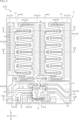
- FIG. 1 is a plan view of a semiconductor device according to a first embodiment of the present disclosure.
- FIG. 2 is a plan view corresponding to FIG. 1, and the illustration of the fourth insulating layer, the plurality of first vias, the plurality of second vias, and the plurality of heat dissipation layers is omitted.
- FIG. 3 is a plan view corresponding to FIG. 2, and illustration of the third insulating layer and the plurality of intermediate layers is omitted.
- FIG. 4 is a plan view corresponding to FIG. 3, in which the second insulating layer is omitted and the first semiconductor element, the second semiconductor element, and the IC are transparent.
- FIG. 5 is a bottom view of the semiconductor device shown in FIG. 1, with the cover layer being transparent.
- FIG. 6 is a sectional view taken along line VI-VI in FIG. 4.
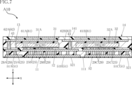
- FIG. 7 is a cross-sectional view taken along line VII-VII in FIG. 4.
- FIG. 8 is a cross-sectional view taken along line VIII-VIII in FIG. 4.
- FIG. 9 is a sectional view taken along line IX-IX in FIG. 4.
- FIG. 10 is a cross-sectional view taken along line XX in FIG. 4.
- FIG. 11 is a partially enlarged view of FIG. 4.
- FIG. 12 is a sectional view taken along line XII-XII in FIG. 11.
- FIG. 13 is a cross-sectional view of a semiconductor device according to a second embodiment of the present disclosure.
- FIG. 14 is a cross-sectional view of the semiconductor device shown in FIG.
- FIG. 15 is a partially enlarged sectional view of the semiconductor device shown in FIG. 13.
- FIG. 16 is a plan view of a semiconductor device according to a third embodiment of the present disclosure.
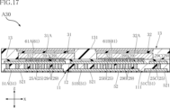
- FIG. 17 is a cross-sectional view taken along line XVII-XVII in FIG. 16.
- FIG. 18 is a cross-sectional view taken along line XVIII-XVIII in FIG. 16.
- FIG. 19 is a cross-sectional view taken along line XIX-XIX in FIG. 16.
- FIG. 20 is a plan view of a semiconductor device according to a fourth embodiment of the present disclosure.
- FIG. 21 is a cross-sectional view taken along line XXI-XXI in FIG. 20.
- 22 is a cross-sectional view taken along line XXII-XXII in FIG. 20.
- FIG. 23 is a cross-sectional view taken along line XXIII-XXIII in FIG. 20.
- the semiconductor device A10 includes a first insulating layer 11, a second insulating layer 12, a third insulating layer 13, a fourth insulating layer 14, a first wiring 21, a second wiring 22, a third wiring 23, a fourth wiring 24, and a plurality of power wiring 25 , a plurality of control wirings 26 , a plurality of communication wirings 29 , a first semiconductor element 31 , a second semiconductor element 32 , an IC 33 , and a plurality of connection wirings 39 .
- the semiconductor device A10 includes a plurality of first vias 41, a plurality of second vias 42, a plurality of third vias 43, a plurality of fourth vias 44, a plurality of fifth vias 45, a plurality of terminals 51, a covering layer 52, It includes a plurality of heat dissipation layers 61 and a plurality of intermediate layers 62.
- the semiconductor device A10 is in the form of a resin package that is surface mounted on a wiring board.
- FIG. 2 omits illustration of the fourth insulating layer 14, the plurality of first vias 41, the plurality of second vias 42, and the plurality of heat dissipation layers 61.
- FIG. 3 omits illustration of the third insulating layer 13 and the plurality of intermediate layers 62 compared to FIG. 2 .
- FIG. 4 omits the illustration of the second insulating layer 12 compared to FIG. 3, and the first semiconductor element 31, the second semiconductor element 32, and the IC 33 are transparent.
- the plurality of transmitted first semiconductor elements 31, second semiconductor elements 32, and ICs 33 are shown by imaginary lines (two-dot chain lines).
- the covering layer 52 is collapsed for convenience of understanding.
- the transparent coating layer 52 is shown in phantom lines.
- the semiconductor device A10 for convenience, an example of the normal direction of the top surface 141 of the fourth insulating layer 14, which will be described later, will be referred to as a "first direction z.”
- An example of a direction perpendicular to the first direction z is referred to as a "second direction x.”
- An example of a direction perpendicular to the first direction z and the second direction x is referred to as a "third direction y.”
- the semiconductor device A10 has a rectangular shape when viewed in the first direction z.
- the semiconductor device A10 converts DC power supplied to the semiconductor device A10 from the outside into AC power using the first semiconductor element 31 and the second semiconductor element 32.
- the semiconductor device A10 is used, for example, as an inverter for driving a motor.
- the semiconductor device A10 can be formed, for example, by the LDS (Laser Direct Structuring) method disclosed in US Patent Application Publication No. 2010/0019370.
- the first insulating layer 11 is located between the first wiring 21 and the second wiring 22 in the first direction z, as shown in FIGS. 9 and 12.
- the first insulating layer 11 contains resin.
- the first insulating layer 11 has a bottom surface 111 facing in the first direction z. When mounting the semiconductor device A10 on a wiring board, the bottom surface 111 faces the wiring board.
- the second insulating layer 12 is located between the first semiconductor element 31, the second semiconductor element 32, and the IC 33, and the first insulating layer 11 in the first direction z.
- the second insulating layer 12 is in contact with the first insulating layer 11.
- the composition of the second insulating layer 12 is the same as that of the first insulating layer 11.
- the third insulating layer 13 is located on the opposite side of the first insulating layer 11 with respect to the second insulating layer 12 in the first direction z.
- the third insulating layer 13 is in contact with the second insulating layer 12.
- the composition of the third insulating layer 13 is the same as that of the first insulating layer 11.
- the fourth insulating layer 14 is located on the opposite side of the second insulating layer 12 with respect to the third insulating layer 13 in the first direction z.
- the fourth insulating layer 14 is in contact with the third insulating layer 13.
- the composition of the fourth insulating layer 14 is the same as that of the first insulating layer 11.
- the fourth insulating layer 14 has a top surface 141 facing opposite to the bottom surface 111 in the first direction z.
- the first semiconductor element 31 faces the second insulating layer 12, as shown in FIGS. 6, 7, and 9. At least a portion of the second semiconductor element 32 is covered with the third insulating layer 13.
- the first semiconductor element 31 is a transistor (switching element) mainly used for power conversion.
- the first semiconductor element 31 is made of a material containing, for example, a nitride semiconductor.
- the first semiconductor element 31 is a HEMT (High Electron Mobility Transistor) made of a material containing gallium nitride (GaN).
- each of the first semiconductor elements 31 has a first main surface 31A, two first electrodes 311, a plurality of second electrodes 312, and a plurality of third electrodes 313.
- the first main surface 31A faces the same side as the top surface 141 of the fourth insulating layer 14 in the first direction z.
- the two first electrodes 311, the plurality of second electrodes 312, and the plurality of third electrodes 313 are located on the opposite side to the side where the first main surface 31A is located in the first direction z. Therefore, the two first electrodes 311 , the plurality of second electrodes 312 , and the plurality of third electrodes 313 face the second insulating layer 12 .
- each of the plurality of second electrodes 312 and the plurality of third electrodes 313 extends in the third direction y.
- Two third electrodes 313 among the plurality of third electrodes 313 are located on both sides of the plurality of second electrodes 312 in the third direction y.
- a current corresponding to the power before being converted by the first semiconductor element 31 flows through the plurality of third electrodes 313 . Therefore, the plurality of third electrodes 313 correspond to the drain of the first semiconductor element 31.
- a current corresponding to the power converted by the first semiconductor element 31 flows through the plurality of second electrodes 312 . Therefore, the plurality of second electrodes 312 correspond to the source of the first semiconductor element 31.
- the two first electrodes 311 are located on both sides of the first semiconductor element 31 in the third direction y.
- a gate voltage for driving the first semiconductor element 31 is applied to either of the two first electrodes 311 .
- the area of each of the two first electrodes 311 is smaller than the area of each of the plurality of second electrodes 312 and the plurality of third electrodes 313.
- the shape and arrangement of each of the two first electrodes 311, the plurality of second electrodes 312, and the plurality of third electrodes 313 in the first semiconductor element 31 are merely examples.
- the second semiconductor element 32 faces the second insulating layer 12, as shown in FIGS. 6, 7, and 10. At least a portion of the second semiconductor element 32 is covered with the third insulating layer 13. The second semiconductor element 32 is separated from the first semiconductor element 31 in the second direction x.
- the first semiconductor element 31 is an element having the same structure and the same function as the second semiconductor element 32. Therefore, in the description of the first semiconductor element 31, content that overlaps with the description of the second semiconductor element 32 will be omitted.
- the second semiconductor element 32 has a second main surface 32A, two fourth electrodes 321, a plurality of fifth electrodes 322, and a plurality of sixth electrodes 323.
- the second main surface 32A faces the same side as the top surface 141 of the fourth insulating layer 14 in the first direction z.
- the two fourth electrodes 321, the plurality of fifth electrodes 322, and the plurality of sixth electrodes 323 are located on the opposite side of the second main surface 32A in the first direction z. Therefore, the two fourth electrodes 321 , the plurality of fifth electrodes 322 , and the plurality of sixth electrodes 323 face the second insulating layer 12 .
- the structure and function of the two fourth electrodes 321 correspond to the structure and function of the two first electrodes 311 of the first semiconductor element 31.
- the structure and function of the plurality of fifth electrodes 322 correspond to the structure and function of the plurality of second electrodes 312 of the first semiconductor element 31.
- the structure and function of the plurality of sixth electrodes 323 correspond to the structure and function of the plurality of third electrodes 313 of the second semiconductor element 32.
- the shape and arrangement of each of the two fourth electrodes 321, the plurality of fifth electrodes 322, and the plurality of sixth electrodes 323 in the second semiconductor element 32 are merely examples.
- the IC 33 faces the second insulating layer 12, as shown in FIGS. 2, 5, and 6.
- IC 33 is covered with third insulating layer 13.
- the IC 33 is located on one side of the first semiconductor element 31 and the second semiconductor element 32 in the third direction y.
- the IC 33 is electrically connected to the first semiconductor element 31 and the second semiconductor element 32.
- the IC 33 is a gate driver that applies a gate voltage to either one of the two fourth electrodes 321 of the second semiconductor element 32 and one of the two first electrodes 311 of the plurality of first semiconductor elements 31.
- IC 33 has a plurality of pads 331.
- the plurality of pads 331 face the second insulating layer 12.
- the plurality of connection wires 39 are accommodated in the second insulating layer 12, as shown in FIGS. 6 to 10. As shown in FIG. 3, each of the plurality of connection wirings 39 overlaps one of the first semiconductor element 31, the second semiconductor element 32, and the IC 33 when viewed in the first direction z. Each of the plurality of connection wirings 39 is connected to one of the first wiring 21 , the third wiring 23 , the plurality of power wirings 25 , and the plurality of control wirings 26 .
- the composition of the plurality of connection wires 39 is the same as the composition of the first wire 21.
- the plurality of connection wires 39 include a plurality of first connection wires 39A, a plurality of second connection wires 39B, and a plurality of third connection wires 39C.
- Each of the plurality of first connection wirings 39A is connected to one of the two first electrodes 311, the plurality of second electrodes 312, and the plurality of third electrodes 313 of the first semiconductor element 31.
- Each of the plurality of second connection wirings 39B is connected to one of the two fourth electrodes 321, the plurality of fifth electrodes 322, and the plurality of sixth electrodes 323 of the second semiconductor element 32.
- the plurality of third connection wirings 39C are individually connected to the plurality of pads 331 of the IC 33.
- the plurality of power wirings 25 are located between the first insulating layer 11 and the second insulating layer 12, as shown in FIGS. 6, 7, 9, and 10. At least a portion of each of the plurality of power lines 25 is accommodated in the second insulating layer 12.
- the composition of the plurality of power wirings 25 is the same as the composition of the first wiring 21.
- the plurality of power wirings 25 include a first power wiring 25A, a second power wiring 25B, and a third power wiring 25C.
- the plurality of second electrodes 312 of the first semiconductor element 31 are electrically connected to the first power wiring 25A via some of the plurality of first connection wirings 39A.
- the plurality of third electrodes 313 of the first semiconductor element 31 are electrically connected to the second power wiring 25B via some of the plurality of first connection wirings 39A.
- the plurality of fifth electrodes 322 of the second semiconductor element 32 are electrically connected to the second power wiring 25B via some of the plurality of second connection wirings 39B.
- the plurality of sixth electrodes 323 of the second semiconductor element 32 are electrically connected to the third power wiring 25C via some of the plurality of second connection wirings 39B.
- the plurality of control wirings 26 are located between the first insulating layer 11 and the second insulating layer 12, as shown in FIGS. 8 and 10. At least a portion of each of the plurality of control wires 26 is accommodated in the second insulating layer 12.
- the composition of the plurality of control wirings 26 is the same as that of the first wiring 21.
- Each of the plurality of control wirings 26 is electrically connected to one of the plurality of pads 331 of the IC 33 via one of the plurality of third connection wirings 39C.
- the first wiring 21 is located between the first insulating layer 11 and the second insulating layer 12, as shown in FIG. At least a portion of the first wiring 21 is accommodated in the second insulating layer 12.
- the composition of the first wiring 21 includes at least copper (Cu).
- the first wiring 21 is electrically connected to one of the two first electrodes 311 of the first semiconductor element 31 via one of the plurality of first connection wirings 39A. Further, the first wiring 21 is electrically connected to one of the plurality of pads 331 of the IC 33 via one of the plurality of third connection wirings 39C. In the first wiring 21, a current I1 flows from one of the plurality of pads 331 of the IC 33 toward one of the two first electrodes 311 of the first semiconductor element 31.
- the second wiring 22 is located on the opposite side of the second insulating layer 12 with respect to the first insulating layer 11. At least a portion of the second wiring 22 is accommodated in the first insulating layer 11.
- the composition of the second wiring 22 is the same as that of the first wiring 21.
- the second wiring 22 is electrically connected to the plurality of second electrodes 312 of the first semiconductor element 31 via a first terminal 51A, which will be described later, and a first power wiring 25A. Further, the second wiring 22 is electrically connected to one of the plurality of pads 331 of the IC 33 via one of the plurality of control wirings 26.
- a current I2 flows from the plurality of second electrodes 312 of the first semiconductor element 31 toward one of the plurality of pads 331 of the IC 33. Therefore, the direction of the current I2 is opposite to the direction of the current I1 flowing through the first wiring 21.
- the first wiring 21 overlaps the second wiring 22 when viewed in the first direction z.
- the distance D between the first wiring 21 and the second wiring 22 in the first direction z is different from the first direction z and the direction in which the current I1 flows in the first wiring 21. It is shorter than the first dimension B1 of the first wiring 21 in the orthogonal direction.
- the first dimension B1 is larger than the second dimension B2 of the second wiring 22 in the direction perpendicular to the first direction z and the direction in which the current I2 flows in the second wiring 22. is small.
- the third wiring 23 is located between the first insulating layer 11 and the second insulating layer 12, as shown in FIG. At least a portion of the third wiring 23 is accommodated in the second insulating layer 12.
- the composition of the third wiring 23 is the same as that of the first wiring 21.
- the third wiring 23 is electrically connected to one of the two fourth electrodes 321 of the second semiconductor element 32 via one of the plurality of second connection wirings 39B. Further, the third wiring 23 is electrically connected to one of the plurality of pads 331 of the IC 33 via one of the plurality of third connection wirings 39C. In the third wiring 23, a current flows from one of the plurality of pads 331 of the IC 33 toward one of the two fourth electrodes 321 of the second semiconductor element 32.
- the fourth wiring 24 is located on the opposite side of the second insulating layer 12 with respect to the first insulating layer 11. At least a portion of the fourth wiring 24 is accommodated in the first insulating layer 11.
- the composition of the fourth wiring 24 is the same as that of the first wiring 21.
- the fourth wiring 24 is electrically connected to the plurality of fifth electrodes 322 of the second semiconductor element 32 via a second terminal 51B, which will be described later, and a second power wiring 25B. Further, the fourth wiring 24 is electrically connected to one of the plurality of pads 331 of the IC 33 via one of the plurality of control wirings 26.
- the fourth wiring 24 a current flows from the plurality of fifth electrodes 322 of the second semiconductor element 32 toward any one of the plurality of pads 331 of the IC 33 . Therefore, the direction of the current flowing through the fourth wiring 24 is opposite to the direction of the current flowing through the third wiring 23.
- the third wiring 23 overlaps the fourth wiring 24 when viewed in the first direction z.
- the conduction path length L1 of the first wiring 21 is longer than the conduction path length L2 of the third wiring 23.
- the conduction path length L1 is the length of the shortest path in the first wiring 21 among the conduction paths from any of the plurality of pads 331 of the IC 33 to either of the two first electrodes 311 of the first semiconductor element 31.
- the conduction path length L2 is the length of the shortest path in the second wiring 22 among the conduction paths from any of the plurality of pads 331 of the IC 33 to either of the two second electrodes 312 of the second semiconductor element 32. .
- the plurality of communication wirings 29 are accommodated in the first insulating layer 11, as shown in FIGS. 6 to 10. Each of the plurality of communication wirings 29 is connected to one of the first wiring 21 , the second wiring 22 , the plurality of power wirings 25 , and the plurality of control wirings 26 , the second wiring 22 , the fourth wiring 24 , and the plurality of terminals 51 and are connected to either. As shown in FIG. 5, the plurality of interconnections 29 are surrounded by the periphery of the bottom surface 111 of the first insulating layer 11 when viewed in the first direction z. The composition of the plurality of interconnections 29 is the same as the composition of the first interconnection 21.
- the plurality of communication wirings 29 connect the plurality of first communication wirings 29A, the plurality of second communication wirings 29B, the plurality of third communication wirings 29C, and the plurality of fourth communication wirings 29D. include.
- the plurality of first connection wirings 29A are connected to the first power wiring 25A and a first terminal 51A, which will be described later.
- the plurality of second connection wirings 29B It is connected to the second power wiring 25B and a second terminal 51B, which will be described later.
- the plurality of third communication wirings 29C are connected to the third power wiring 25C and a third terminal 51C, which will be described later.
- each of the plurality of fourth connection wirings 29D is connected to one of the first wiring 21, the third wiring 23, and the plurality of control wirings 26, the second wiring 22, the fourth It is connected to the wiring 24 and to each of a plurality of control terminals 51D, which will be described later.
- the plurality of terminals 51 are located on the opposite side of the second insulating layer 12 with respect to the first insulating layer 11. As shown in FIG. 5, each of the plurality of terminals 51 is connected to one of the plurality of connection wires 29. Thereby, each of the plurality of terminals 51 is electrically connected to at least one of the first semiconductor element 31, the second semiconductor element 32, and the IC 33. The plurality of terminals 51 are in contact with the first insulating layer 11. In the semiconductor device A10, at least a portion of each of the plurality of terminals 51 is accommodated in the first insulating layer 11. The composition of the plurality of terminals 51 is the same as that of the first wiring 21.
- the plurality of terminals 51 include a third terminal 51C, a second terminal 51B, a third terminal 51C, and a plurality of control terminals 51D.
- the first terminal 51A is electrically connected to the first power wiring 25A via a plurality of first connection wirings 29A.
- the second wiring 22 is connected to the first terminal 51A.
- the third terminal 51C is electrically connected to the second power wiring 25B via a plurality of third communication wirings 29C.
- DC power to be converted by the first semiconductor element 31 and the second semiconductor element 32 is input to the first terminal 51A and the third terminal 51C.
- the first terminal 51A is a negative electrode (N terminal).
- the third terminal 51C is a positive electrode (P terminal).
- the second terminal 51B is electrically connected to the second power wiring 25B via a plurality of second connection wirings 29B.
- AC power converted by the first semiconductor element 31 and the second semiconductor element 32 is output from the second terminal 51B.
- the fourth wiring 24 is connected to the second terminal 51B.
- Each of the plurality of control terminals 51D is electrically connected to any one of the first wiring 21, the third wiring 23, and the plurality of control wirings 26 via any one of the plurality of fourth connection wirings 29D. Therefore, each of the plurality of control terminals 51D is electrically connected to the IC 33. Electric power for driving the IC 33 is input to one of the plurality of control terminals 51D. An electrical signal to the IC 33 is input to one of the plurality of control terminals 51D. Further, an electric signal from the IC 33 is outputted from one of the plurality of control terminals 51D.
- the covering layer 52 is located on the opposite side of the second insulating layer 12 with respect to the first insulating layer 11.
- the covering layer 52 covers the bottom surface 111 as a part of the first insulating layer 11 .
- Covering layer 52 is an insulator.
- the covering layer 52 is, for example, a solder resist.
- the second wiring 22 and the fourth wiring 24 are covered with a covering layer 52.
- the covering layer 52 is provided with a plurality of openings 521.
- the plurality of openings 521 penetrate the covering layer 52 in the first direction z. From each of the plurality of openings 521, one of the plurality of terminals 51 is exposed to the outside. Thereby, when mounting the semiconductor device A10 on a wiring board, each of the plurality of terminals 51 can be electrically bonded to the wiring board through solder.
- the plurality of heat dissipation layers 61 are located on the opposite side of the second insulating layer 12 with respect to the third insulating layer 13.
- the semiconductor device A10 at least a portion of each of the plurality of heat dissipation layers 61 is accommodated in the fourth insulating layer 14.
- the plurality of heat dissipation layers 61 are in contact with the fourth insulating layer 14 .
- the plurality of heat dissipation layers 61 are exposed to the outside from the top surface 141 of the fourth insulating layer 14 .
- the composition of the plurality of heat dissipation layers 61 is the same as the composition of the first wiring 21.
- the plurality of heat dissipation layers 61 include a first heat dissipation layer 61A and a second heat dissipation layer 61B.
- the first heat dissipation layer 61A and the second heat dissipation layer 61B are separated from each other in the second direction x.
- the first heat dissipation layer 61A overlaps the first semiconductor element 31 when viewed in the first direction z.
- the second heat dissipation layer 61B overlaps the second semiconductor element 32 when viewed in the first direction z.
- the plurality of intermediate layers 62 are located on the opposite side of the second insulating layer 12 with respect to the third insulating layer 13, and the third insulating layer 13 and the plurality of heat dissipating layers 61 located between. At least a portion of each of the plurality of intermediate layers 62 is accommodated in the third insulating layer 13. The plurality of intermediate layers 62 are in contact with the fourth insulating layer 14 . Therefore, the fourth insulating layer 14 is located between the plurality of intermediate layers 62 and the plurality of heat dissipation layers 61.
- the composition of the plurality of intermediate layers 62 is the same as that of the first wiring 21.
- the plurality of intermediate layers 62 include a first intermediate layer 62A, a second intermediate layer 62B, and a third intermediate layer 62C.
- the first intermediate layer 62A and the second intermediate layer 62B are separated from each other in the second direction x.
- the first intermediate layer 62A overlaps the first semiconductor element 31 and the first heat dissipation layer 61A.
- the first intermediate layer 62A is separated from the first semiconductor element 31.
- the second intermediate layer 62B overlaps the second semiconductor element 32 and the second heat dissipation layer 61B.
- the second intermediate layer 62B is separated from the second semiconductor element 32.
- the third intermediate layer 62C is located between the first intermediate layer 62A and the second intermediate layer 62B in the second direction x.
- the third intermediate layer 62C overlaps the IC 33 when viewed in the first direction z.
- the third intermediate layer 62C is separated from the IC 33.
- the plurality of first vias 41 are accommodated in the fourth insulating layer 14, as shown in FIG.
- the plurality of first vias 41 are connected to the first heat dissipation layer 61A and the first intermediate layer 62A.
- the first intermediate layer 62A is electrically connected to the first heat dissipation layer 61A.
- the composition of the plurality of first vias 41 is the same as the composition of the first wiring 21.
- the plurality of second vias 42 are accommodated in the fourth insulating layer 14, as shown in FIGS. 6 and 10.
- the plurality of second vias 42 are connected to the second heat dissipation layer 61B and the second intermediate layer 62B.
- the second intermediate layer 62B is electrically connected to the second heat dissipation layer 61B.
- the composition of the plurality of second vias 42 is the same as the composition of the first wiring 21.
- the plurality of third vias 43 are accommodated in the second insulating layer 12 and the third insulating layer 13, as shown in FIGS. 6 and 7.
- the plurality of third vias 43 are connected to the first intermediate layer 62A and the first power wiring 25A. Thereby, the first intermediate layer 62A is electrically connected to the first power wiring 25A.
- the composition of the plurality of third vias 43 is the same as the composition of the first wiring 21.
- the plurality of fourth vias 44 are accommodated in the second insulating layer 12 and the third insulating layer 13, as shown in FIGS. 6 and 7.
- the plurality of fourth vias 44 are connected to the second intermediate layer 62B and the second power wiring 25B. Thereby, the second intermediate layer 62B is electrically connected to the second power wiring 25B.
- the composition of the plurality of fourth vias 44 is the same as the composition of the first wiring 21.
- the plurality of fifth vias 45 are accommodated in the second insulating layer 12 and the third insulating layer 13, as shown in FIG.
- the plurality of fifth vias 45 are electrically connected to the second intermediate layer 62B and one of the plurality of control wirings 26.
- the semiconductor device A10 includes a first wiring 21 electrically connected to the first electrode 311 of the first semiconductor element 31 and a second wiring 22 electrically connected to the second electrode 312 of the first semiconductor element 31.
- the direction of the current I2 flowing through the second wiring 22 is opposite to the direction of the current I1 flowing through the first wiring 21.
- the first wiring 21 overlaps the second wiring 22 when viewed in the first direction z.
- the distance D between the first wiring 21 and the second wiring 22 in the first direction z is the first dimension B1 of the first wiring 21 (perpendicular to the direction in which the current I1 flows in the first direction z and the first wiring 21). (dimension in direction). With this configuration, a back electromotive force is generated in the first wiring 21 as the second wiring 22 becomes conductive.
- a gate voltage for driving the first semiconductor element 31 is applied to the first electrode 311 of the first semiconductor element 31. Therefore, by reducing the parasitic inductance in the first wiring 21, switching loss of the first semiconductor element 31 can be suppressed.
- the first dimension B1 of the first wiring 21 is shorter than the second dimension B2 of the second wiring 22 (the dimension in the direction orthogonal to the direction in which the current I2 flows in the first direction z and the second wiring 22).
- the area of the first wiring 21 overlapping the second wiring 22 is further increased when viewed in the first direction z.
- the back electromotive force generated in the first wiring 21 due to the mutual inductance acting on the first wiring 21 and the second wiring 22 becomes larger. Therefore, the parasitic inductance in the first wiring 21 can be reduced more effectively.
- the semiconductor device A10 further includes a first insulating layer 11 located between the first wiring 21 and the second wiring 22 in the first direction z.
- the first insulating layer 11 contains resin. At least a portion of the second wiring 22 is accommodated in the first insulating layer 11.
- the semiconductor device A10 includes a second insulating layer 12 located between the first semiconductor element 31 and the first insulating layer 11 in the first direction z, and a second insulating layer 12 located opposite to the first insulating layer 11 with respect to the second insulating layer 12. It further includes a third insulating layer 13 located on the side. At least a portion of the first semiconductor element 31 is covered with the third insulating layer 13.
- the first wiring 21 is located between the first insulating layer 11 and the second insulating layer 12.
- the semiconductor device A10 further includes a heat dissipation layer 61 located on the opposite side of the second insulating layer 12 with respect to the third insulating layer 13.
- the heat dissipation layer 61 is exposed to the outside.
- the heat dissipation layer 61 overlaps the first semiconductor element 31 when viewed in the first direction z.
- the semiconductor device A10 further includes an intermediate layer 62 located on the opposite side of the second insulating layer 12 with respect to the third insulating layer 13 and between the third insulating layer 13 and the heat dissipation layer 61.
- the intermediate layer 62 is in contact with the third insulating layer 13 and is away from the first semiconductor element 31 .
- the intermediate layer 62 is electrically connected to one of the plurality of power wirings 25 to which the first semiconductor element 31 is electrically connected, and to the heat dissipation layer 61 . With this configuration, heat generated from the first semiconductor element 31 is conducted to the intermediate layer 62 via any one of the plurality of power wirings 25.
- the intermediate layer 62 overlaps the first semiconductor element 31 and the heat dissipation layer 61 . Therefore, the heat generated from the first semiconductor element 31 can be more smoothly conducted to the heat dissipation layer 61. Further, the intermediate layer 62 has the effect of reducing noise generated from the first semiconductor element 31 and noise entering the semiconductor device A10 from the outside.
- FIGS. 13 to 15 A semiconductor device A20 according to a second embodiment of the present disclosure will be described based on FIGS. 13 to 15.
- the same or similar elements as those of the semiconductor device A10 described above are denoted by the same reference numerals, and redundant explanation will be omitted.
- the cross-sectional position in FIG. 13 is the same (or substantially the same) as the cross-sectional position in FIG. 6 showing the semiconductor device A10.
- the cross-sectional position in FIG. 14 is the same (or substantially the same) as the cross-sectional position in FIG. 9 showing the semiconductor device A10.
- the cross-sectional position in FIG. 15 is the same (or substantially the same) as the cross-sectional position in FIG. 12 showing the semiconductor device A10.
- the configuration of the first insulating layer 11 is different from the configuration of the semiconductor device A10.
- the second wiring 22, the fourth wiring 24, and the plurality of terminals 51 are located on the opposite side of the plurality of connection wirings 29 with respect to the bottom surface 111 of the first insulating layer 11. . Therefore, the second wiring 22, the fourth wiring 24, and the plurality of terminals 51 are not accommodated in the first insulating layer 11 and are in contact with the bottom surface 111.
- the first insulating layer 11 contains a silicon compound.
- the silicon compound is either silicon dioxide (SiO 2 ) or silicon nitride (Si 3 N 4 ).
- the first insulating layer 11 is formed by plasma CVD (Chemical Vapor Deposition) under relatively low temperature conditions.
- the dimension of the first insulating layer 11 in the first direction z is smaller than the dimension in the semiconductor device A10. Therefore, the distance D between the first wiring 21 and the second wiring 22 in the first direction z is even shorter than the distance D in the semiconductor device A10.
- the semiconductor device A20 includes a first wiring 21 electrically connected to the first electrode 311 of the first semiconductor element 31 and a second wiring 22 electrically connected to the second electrode 312 of the first semiconductor element 31.
- the direction of the current I2 flowing through the second wiring 22 is opposite to the direction of the current I1 flowing through the first wiring 21.
- the first wiring 21 overlaps the second wiring 22 when viewed in the first direction z.
- the distance D between the first wiring 21 and the second wiring 22 in the first direction z is the first dimension B1 of the first wiring 21 (perpendicular to the direction in which the current I1 flows in the first direction z and the first wiring 21). (dimension in direction).
- the semiconductor device A20 even in the semiconductor device A20, it is possible to reduce the parasitic inductance in the wiring of the semiconductor device A20. Further, the semiconductor device A20 has the same configuration as the semiconductor device A10, so that the same effects as the semiconductor device A10 can be achieved.
- the first insulating layer 11 contains a silicon compound.
- a semiconductor device A30 according to a third embodiment of the present disclosure will be described based on FIGS. 16 to 19.
- the same or similar elements as those of the semiconductor device A10 described above are denoted by the same reference numerals, and redundant explanation will be omitted.
- the structure of the intermediate layer 62, the fourth insulating layer 14, the plurality of intermediate layers 62, the plurality of first vias 41, the plurality of second vias 42, the plurality of third vias 43, and the plurality of fourth is that the via 44 and the plurality of fifth vias 45 are not provided.
- the third insulating layer 13 has a top surface 131 facing away from the bottom surface 111 of the first insulating layer 11 in the first direction z. At least a portion of each of the plurality of heat dissipation layers 61 is accommodated in the third insulating layer 13. The plurality of heat dissipation layers 61 are exposed to the outside from the top surface 131. Each of the plurality of heat dissipation layers 61 is electrically insulated from any of the plurality of power wirings 25 and the plurality of control wirings 26.
- the semiconductor device A30 includes a first wiring 21 electrically connected to the first electrode 311 of the first semiconductor element 31 and a second wiring 22 electrically connected to the second electrode 312 of the first semiconductor element 31.
- the direction of the current I2 flowing through the second wiring 22 is opposite to the direction of the current I1 flowing through the first wiring 21.
- the first wiring 21 overlaps the second wiring 22 when viewed in the first direction z.
- the distance D between the first wiring 21 and the second wiring 22 in the first direction z is the first dimension B1 of the first wiring 21 (perpendicular to the direction in which the current I1 flows in the first direction z and the first wiring 21). (dimension in direction).
- the semiconductor device A30 even in the semiconductor device A30, it is possible to reduce the parasitic inductance in the wiring of the semiconductor device A30. Furthermore, the semiconductor device A30 has the same configuration as the semiconductor device A10, so that it can achieve the same effects as the semiconductor device A10.
- the semiconductor device A30 does not include the fourth insulating layer 14 and the intermediate layer 62, unlike the semiconductor device A10. At least a portion of the heat dissipation layer 61 is accommodated in the third insulating layer 13. The heat dissipation layer 61 is in contact with the third insulating layer 13 and exposed to the outside from the third insulating layer 13 . By adopting this configuration, the dimensions of the semiconductor device A30 in the first direction z can be reduced while suppressing a decrease in the heat dissipation performance of the semiconductor device A30.
- a semiconductor device A40 according to a fourth embodiment of the present disclosure will be described based on FIGS. 20 to 23.
- the same or similar elements as those of the semiconductor device A10 described above are denoted by the same reference numerals, and redundant explanation will be omitted.
- the semiconductor device A40 differs from the previously described semiconductor device A30 in the configuration of the third insulating layer 13 and the absence of a plurality of heat dissipation layers 61.
- the first main surface 31A of the first semiconductor element 31 and the second main surface 32A of the second semiconductor element 32 are exposed to the outside from the top surface 131 of the third insulating layer 13. are doing.
- Each of the first main surface 31A and the second main surface 32A is flush with the top surface 131. Therefore, the dimension of the third insulating layer 13 in the first direction z is smaller than the dimension of the semiconductor device A30.
- the semiconductor device A40 includes a first wiring 21 electrically connected to the first electrode 311 of the first semiconductor element 31 and a second wiring 22 electrically connected to the second electrode 312 of the first semiconductor element 31.
- the direction of the current I2 flowing through the second wiring 22 is opposite to the direction of the current I1 flowing through the first wiring 21.
- the first wiring 21 overlaps the second wiring 22 when viewed in the first direction z.
- the distance D between the first wiring 21 and the second wiring 22 in the first direction z is the first dimension B1 of the first wiring 21 (perpendicular to the direction in which the current I1 flows in the first direction z and the first wiring 21). (dimension in direction).
- the semiconductor device A40 even in the semiconductor device A40, it is possible to reduce the parasitic inductance in the wiring of the semiconductor device A40. Furthermore, the semiconductor device A40 has the same configuration as the semiconductor device A10, so that it can achieve the same effects as the semiconductor device A10.
- the semiconductor device A40 does not include the heat dissipation layer 61, unlike the semiconductor device A30.
- the first main surface 31A of the first semiconductor element 31 is exposed to the outside from the third insulating layer 13. Further, the first main surface 31A is flush with the third insulating layer 13.
- Appendix 1 a first semiconductor element having a first electrode and a second electrode; a first wiring conductive to the first electrode; a second wiring conductive to the second electrode; The direction of the current flowing through the second wiring is opposite to the direction of the current flowing through the first wiring, When viewed in the first direction, the first wiring overlaps the second wiring, The distance between the first wiring and the second wiring in the first direction is the same as the distance between the first wiring and the second wiring in the direction perpendicular to the first direction and the direction in which current flows in the first wiring.
- a semiconductor device that is shorter than its dimensions.
- Addendum 2 The semiconductor according to supplementary note 1, wherein the first dimension is smaller than the second dimension of the second wiring in a direction perpendicular to the first direction and the direction in which current flows in the second wiring.
- Appendix 3 The semiconductor device according to appendix 2, further comprising a first insulating layer located between the first wiring and the second wiring in the first direction.
- Appendix 4 The first insulating layer includes resin, The semiconductor device according to appendix 3, wherein at least a portion of the second wiring is accommodated in the first insulating layer.
- Appendix 5 The semiconductor device according to appendix 3, wherein the first insulating layer contains a silicon compound.
- Appendix 6 further comprising a second insulating layer located between the first semiconductor element and the first insulating layer in the first direction, The first wiring is located between the first insulating layer and the second insulating layer, The semiconductor device according to appendix 4 or 5, wherein the first electrode and the second electrode face the second insulating layer.
- Appendix 7 The second insulating layer includes resin, The semiconductor device according to appendix 6, wherein at least a portion of the first wiring is accommodated in the second insulating layer.
- Appendix 8 further comprising a plurality of power wirings located between the first insulating layer and the second insulating layer, The first semiconductor element has a third electrode facing the second insulating layer, 8.
- each of the second electrode and the third electrode is electrically connected to any one of the plurality of power wirings.
- Appendix 9 a second semiconductor element having a fourth electrode and a fifth electrode facing the second insulating layer; further comprising a third wiring located between the first insulating layer and the second insulating layer and electrically connected to the fourth electrode, The fifth electrode is electrically connected to any of the plurality of power wirings, The semiconductor device according to appendix 8, wherein the conduction path length of the first wiring is longer than the conduction path length of the third wiring.
- Appendix 10 The semiconductor device according to appendix 9, wherein the second wiring is electrically connected to the second electrode via any one of the plurality of power wirings.
- Appendix 11 further comprising an IC located on the opposite side of the first insulating layer with respect to the second insulating layer, The semiconductor device according to appendix 10, wherein the first wiring, the second wiring, and the third wiring are electrically connected to the IC.
- Appendix 12 further comprising a plurality of terminals located on the opposite side of the second insulating layer with respect to the first insulating layer, Each of the plurality of terminals is electrically connected to at least one of the first semiconductor element, the second semiconductor element, and the IC, The semiconductor device according to appendix 11, wherein the plurality of terminals are in contact with the first insulating layer.
- Appendix 13 further comprising a coating layer located on the opposite side of the second insulating layer with respect to the first insulating layer and covering a part of the first insulating layer, The covering layer is an insulator, The semiconductor device according to appendix 12, wherein the second wiring is covered with the covering layer.
- Appendix 14 further comprising a third insulating layer located on the opposite side of the first insulating layer with respect to the second insulating layer, 14. The semiconductor device according to any one of appendices 8 to 13, wherein at least a portion of the first semiconductor element is covered with the third insulating layer.
- Appendix 15 The first semiconductor element has a main surface facing opposite to the side where the first electrode and the second electrode are located in the first direction, The semiconductor device according to appendix 14, wherein the main surface is exposed from the third insulating layer.
- Appendix 16 further comprising a heat dissipation layer located on the opposite side of the second insulating layer with respect to the third insulating layer, The semiconductor device according to appendix 14, wherein the heat dissipation layer overlaps the first semiconductor element when viewed in the first direction.
- Appendix 17 further comprising an intermediate layer located on the opposite side of the second insulating layer with respect to the third insulating layer and between the third insulating layer and the heat dissipation layer, The intermediate layer is in contact with the third insulating layer and is separated from the first semiconductor element, When viewed in the first direction, the intermediate layer overlaps the first semiconductor element and the heat dissipation layer, 17.
- the semiconductor device according to appendix 16 wherein the intermediate layer is electrically connected to any one of the plurality of power wirings and the heat dissipation layer.
- Appendix 18 further comprising a fourth insulating layer located between the intermediate layer and the heat dissipation layer, 18.
- A10, A20, A30, A40 Semiconductor device 11: First insulating layer 111: Bottom surface 12: Second insulating layer 13: Third insulating layer 14: Fourth insulating layer 141: Top surface 21: First wiring 22: Second Wiring 23: Third wiring 24: Fourth wiring 25: Power wiring 25A: First power wiring 25B: Second power wiring 25C: Third power wiring 26: Control wiring 29: Communication wiring 29A: First communication wiring 29B: First 2 connection wiring 29C: 3rd connection wiring 29D: 4th connection wiring 31: 1st semiconductor element 31A: 1st principal surface 311: 1st electrode 312: 2nd electrode 313: 3rd electrode 32: 2nd semiconductor element 32A: Second main surface 321: Fourth electrode 322: Fifth electrode 323: Sixth electrode 33: IC 331: Pad 39: Connection wiring 39A: First connection wiring 39B: Second connection wiring 39C: Third connection wiring 41: Third connection wiring 1 via 42: 2nd via 43: 3rd via 44: 4th via 45: 5th via 51: Terminal 51
Landscapes
- Semiconductor Integrated Circuits (AREA)
Priority Applications (1)
| Application Number | Priority Date | Filing Date | Title |
|---|---|---|---|
| JP2024523039A JPWO2023228782A1 (https=) | 2022-05-27 | 2023-05-12 |
Applications Claiming Priority (2)
| Application Number | Priority Date | Filing Date | Title |
|---|---|---|---|
| JP2022087151 | 2022-05-27 | ||
| JP2022-087151 | 2022-05-27 |
Publications (1)
| Publication Number | Publication Date |
|---|---|
| WO2023228782A1 true WO2023228782A1 (ja) | 2023-11-30 |
Family
ID=88919078
Family Applications (1)
| Application Number | Title | Priority Date | Filing Date |
|---|---|---|---|
| PCT/JP2023/017924 Ceased WO2023228782A1 (ja) | 2022-05-27 | 2023-05-12 | 半導体装置 |
Country Status (2)
| Country | Link |
|---|---|
| JP (1) | JPWO2023228782A1 (https=) |
| WO (1) | WO2023228782A1 (https=) |
Citations (3)
| Publication number | Priority date | Publication date | Assignee | Title |
|---|---|---|---|---|
| JP2004014862A (ja) * | 2002-06-07 | 2004-01-15 | Nissan Motor Co Ltd | 配線構造 |
| WO2021205926A1 (ja) * | 2020-04-08 | 2021-10-14 | ローム株式会社 | 半導体装置 |
| WO2022091288A1 (ja) * | 2020-10-29 | 2022-05-05 | 三菱電機株式会社 | 半導体パッケージ、半導体装置および電力変換装置 |
-
2023
- 2023-05-12 JP JP2024523039A patent/JPWO2023228782A1/ja active Pending
- 2023-05-12 WO PCT/JP2023/017924 patent/WO2023228782A1/ja not_active Ceased
Patent Citations (3)
| Publication number | Priority date | Publication date | Assignee | Title |
|---|---|---|---|---|
| JP2004014862A (ja) * | 2002-06-07 | 2004-01-15 | Nissan Motor Co Ltd | 配線構造 |
| WO2021205926A1 (ja) * | 2020-04-08 | 2021-10-14 | ローム株式会社 | 半導体装置 |
| WO2022091288A1 (ja) * | 2020-10-29 | 2022-05-05 | 三菱電機株式会社 | 半導体パッケージ、半導体装置および電力変換装置 |
Also Published As
| Publication number | Publication date |
|---|---|
| JPWO2023228782A1 (https=) | 2023-11-30 |
Similar Documents
| Publication | Publication Date | Title |
|---|---|---|
| US9236321B2 (en) | Semiconductor device and manufacturing method thereof | |
| US11749578B2 (en) | Semiconductor module, power semiconductor module, and power electronic equipment using the semiconductor module or the power semiconductor module | |
| US20200235067A1 (en) | Electronic device flip chip package with exposed clip | |
| JP2018117054A (ja) | 半導体装置および電力変換装置 | |
| JP2019067951A (ja) | 半導体装置 | |
| WO2021200166A1 (ja) | 半導体装置 | |
| CN118805253A (zh) | 半导体装置以及半导体模块 | |
| CN111490016A (zh) | 半导体管芯及其制造方法和容纳管芯的封装件 | |
| WO2023228782A1 (ja) | 半導体装置 | |
| WO2022130906A1 (ja) | 半導体装置 | |
| WO2025142335A1 (ja) | 半導体装置 | |
| CN115398608A (zh) | 半导体器件 | |
| US20250380362A1 (en) | Circuit assembly with two circuit carriers and a semiconductor component | |
| JP2024027256A (ja) | 半導体装置および半導体素子 | |
| JP7798800B2 (ja) | 半導体装置 | |
| WO2023095659A1 (ja) | 半導体装置 | |
| JP2023134143A (ja) | 半導体モジュール、半導体装置、及び車両 | |
| WO2025057452A1 (ja) | 半導体装置 | |
| JP7838443B2 (ja) | 半導体装置 | |
| WO2026042579A1 (ja) | 半導体装置 | |
| JP7837876B2 (ja) | 半導体装置 | |
| US20260075923A1 (en) | Semiconductor apparatus | |
| US20240395723A1 (en) | Semiconductor device and method for manufacturing semiconductor device | |
| WO2023199808A1 (ja) | 半導体装置 | |
| CN118435350A (zh) | 半导体装置 |
Legal Events
| Date | Code | Title | Description |
|---|---|---|---|
| 121 | Ep: the epo has been informed by wipo that ep was designated in this application |
Ref document number: 23811656 Country of ref document: EP Kind code of ref document: A1 |
|
| WWE | Wipo information: entry into national phase |
Ref document number: 2024523039 Country of ref document: JP |
|
| NENP | Non-entry into the national phase |
Ref country code: DE |
|
| 122 | Ep: pct application non-entry in european phase |
Ref document number: 23811656 Country of ref document: EP Kind code of ref document: A1 |