WO2023228782A1 - Semiconductor device - Google Patents
Semiconductor device Download PDFInfo
- Publication number
- WO2023228782A1 WO2023228782A1 PCT/JP2023/017924 JP2023017924W WO2023228782A1 WO 2023228782 A1 WO2023228782 A1 WO 2023228782A1 JP 2023017924 W JP2023017924 W JP 2023017924W WO 2023228782 A1 WO2023228782 A1 WO 2023228782A1
- Authority
- WO
- WIPO (PCT)
- Prior art keywords
- wiring
- insulating layer
- semiconductor device
- semiconductor element
- layer
- Prior art date
Links
- 239000004065 semiconductor Substances 0.000 title claims abstract description 259
- 239000010410 layer Substances 0.000 claims description 338
- 230000017525 heat dissipation Effects 0.000 claims description 55
- 239000011347 resin Substances 0.000 claims description 7
- 229920005989 resin Polymers 0.000 claims description 7
- 150000003377 silicon compounds Chemical class 0.000 claims description 5
- 239000011247 coating layer Substances 0.000 claims description 3
- 239000012212 insulator Substances 0.000 claims description 3
- 230000003071 parasitic effect Effects 0.000 description 12
- 230000000694 effects Effects 0.000 description 8
- VYPSYNLAJGMNEJ-UHFFFAOYSA-N Silicium dioxide Chemical compound O=[Si]=O VYPSYNLAJGMNEJ-UHFFFAOYSA-N 0.000 description 2
- 230000005540 biological transmission Effects 0.000 description 2
- 238000006243 chemical reaction Methods 0.000 description 2
- 239000010949 copper Substances 0.000 description 2
- 239000000463 material Substances 0.000 description 2
- 229910000679 solder Inorganic materials 0.000 description 2
- RYGMFSIKBFXOCR-UHFFFAOYSA-N Copper Chemical compound [Cu] RYGMFSIKBFXOCR-UHFFFAOYSA-N 0.000 description 1
- JMASRVWKEDWRBT-UHFFFAOYSA-N Gallium nitride Chemical compound [Ga]#N JMASRVWKEDWRBT-UHFFFAOYSA-N 0.000 description 1
- 229910052581 Si3N4 Inorganic materials 0.000 description 1
- 229910004298 SiO 2 Inorganic materials 0.000 description 1
- 238000005229 chemical vapour deposition Methods 0.000 description 1
- 229910052802 copper Inorganic materials 0.000 description 1
- 238000010292 electrical insulation Methods 0.000 description 1
- 238000000034 method Methods 0.000 description 1
- 150000004767 nitrides Chemical class 0.000 description 1
- 238000005268 plasma chemical vapour deposition Methods 0.000 description 1
- 235000012239 silicon dioxide Nutrition 0.000 description 1
- 239000000377 silicon dioxide Substances 0.000 description 1
- HQVNEWCFYHHQES-UHFFFAOYSA-N silicon nitride Chemical compound N12[Si]34N5[Si]62N3[Si]51N64 HQVNEWCFYHHQES-UHFFFAOYSA-N 0.000 description 1
Images


Classifications
-
- H—ELECTRICITY
- H01—ELECTRIC ELEMENTS
- H01L—SEMICONDUCTOR DEVICES NOT COVERED BY CLASS H10
- H01L23/00—Details of semiconductor or other solid state devices
- H01L23/12—Mountings, e.g. non-detachable insulating substrates
-
- H—ELECTRICITY
- H01—ELECTRIC ELEMENTS
- H01L—SEMICONDUCTOR DEVICES NOT COVERED BY CLASS H10
- H01L23/00—Details of semiconductor or other solid state devices
- H01L23/34—Arrangements for cooling, heating, ventilating or temperature compensation ; Temperature sensing arrangements
-
- H—ELECTRICITY
- H01—ELECTRIC ELEMENTS
- H01L—SEMICONDUCTOR DEVICES NOT COVERED BY CLASS H10
- H01L25/00—Assemblies consisting of a plurality of individual semiconductor or other solid state devices ; Multistep manufacturing processes thereof
- H01L25/03—Assemblies consisting of a plurality of individual semiconductor or other solid state devices ; Multistep manufacturing processes thereof all the devices being of a type provided for in the same subgroup of groups H01L27/00 - H01L33/00, or in a single subclass of H10K, H10N, e.g. assemblies of rectifier diodes
- H01L25/04—Assemblies consisting of a plurality of individual semiconductor or other solid state devices ; Multistep manufacturing processes thereof all the devices being of a type provided for in the same subgroup of groups H01L27/00 - H01L33/00, or in a single subclass of H10K, H10N, e.g. assemblies of rectifier diodes the devices not having separate containers
- H01L25/07—Assemblies consisting of a plurality of individual semiconductor or other solid state devices ; Multistep manufacturing processes thereof all the devices being of a type provided for in the same subgroup of groups H01L27/00 - H01L33/00, or in a single subclass of H10K, H10N, e.g. assemblies of rectifier diodes the devices not having separate containers the devices being of a type provided for in group H01L29/00
-
- H—ELECTRICITY
- H01—ELECTRIC ELEMENTS
- H01L—SEMICONDUCTOR DEVICES NOT COVERED BY CLASS H10
- H01L25/00—Assemblies consisting of a plurality of individual semiconductor or other solid state devices ; Multistep manufacturing processes thereof
- H01L25/18—Assemblies consisting of a plurality of individual semiconductor or other solid state devices ; Multistep manufacturing processes thereof the devices being of types provided for in two or more different subgroups of the same main group of groups H01L27/00 - H01L33/00, or in a single subclass of H10K, H10N
Definitions
- the present disclosure relates to a semiconductor device.
- Patent Document 1 discloses an example of a semiconductor device including a horizontally structured semiconductor element (HEMT).
- the semiconductor element has a first electrode and a second electrode.
- a semiconductor element is bonded to a die pad.
- the first electrode and the second electrode are electrically connected to a plurality of terminal leads located around the die pad via wires.
- An object of the present disclosure is to provide a semiconductor device that is improved over the conventional semiconductor device. Particularly, in view of the above-mentioned circumstances, one object of the present disclosure is to provide a semiconductor device that can reduce parasitic inductance in wiring.
- a semiconductor device provided by one aspect of the present disclosure includes a first semiconductor element having a first electrode and a second electrode, a first wiring conductive to the first electrode, and a second wiring conductive to the second electrode. Equipped with wiring.
- the direction of the current flowing through the second wiring is opposite to the direction of the current flowing through the first wiring, and the first wiring overlaps the second wiring when viewed in the first direction.
- the distance between the first wiring and the second wiring in the first direction is the same as the distance between the first wiring and the second wiring in the direction perpendicular to the first direction and the direction in which current flows in the first wiring. shorter than the dimensions.
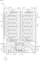
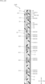
- FIG. 1 is a plan view of a semiconductor device according to a first embodiment of the present disclosure.
- FIG. 2 is a plan view corresponding to FIG. 1, and the illustration of the fourth insulating layer, the plurality of first vias, the plurality of second vias, and the plurality of heat dissipation layers is omitted.
- FIG. 3 is a plan view corresponding to FIG. 2, and illustration of the third insulating layer and the plurality of intermediate layers is omitted.
- FIG. 4 is a plan view corresponding to FIG. 3, in which the second insulating layer is omitted and the first semiconductor element, the second semiconductor element, and the IC are transparent.
- FIG. 5 is a bottom view of the semiconductor device shown in FIG. 1, with the cover layer being transparent.
- FIG. 6 is a sectional view taken along line VI-VI in FIG. 4.
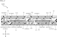
- FIG. 7 is a cross-sectional view taken along line VII-VII in FIG. 4.
- FIG. 8 is a cross-sectional view taken along line VIII-VIII in FIG. 4.
- FIG. 9 is a sectional view taken along line IX-IX in FIG. 4.
- FIG. 10 is a cross-sectional view taken along line XX in FIG. 4.
- FIG. 11 is a partially enlarged view of FIG. 4.
- FIG. 12 is a sectional view taken along line XII-XII in FIG. 11.
- FIG. 13 is a cross-sectional view of a semiconductor device according to a second embodiment of the present disclosure.
- FIG. 14 is a cross-sectional view of the semiconductor device shown in FIG.
- FIG. 15 is a partially enlarged sectional view of the semiconductor device shown in FIG. 13.
- FIG. 16 is a plan view of a semiconductor device according to a third embodiment of the present disclosure.
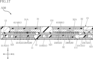
- FIG. 17 is a cross-sectional view taken along line XVII-XVII in FIG. 16.
- FIG. 18 is a cross-sectional view taken along line XVIII-XVIII in FIG. 16.
- FIG. 19 is a cross-sectional view taken along line XIX-XIX in FIG. 16.
- FIG. 20 is a plan view of a semiconductor device according to a fourth embodiment of the present disclosure.
- FIG. 21 is a cross-sectional view taken along line XXI-XXI in FIG. 20.
- 22 is a cross-sectional view taken along line XXII-XXII in FIG. 20.
- FIG. 23 is a cross-sectional view taken along line XXIII-XXIII in FIG. 20.
- the semiconductor device A10 includes a first insulating layer 11, a second insulating layer 12, a third insulating layer 13, a fourth insulating layer 14, a first wiring 21, a second wiring 22, a third wiring 23, a fourth wiring 24, and a plurality of power wiring 25 , a plurality of control wirings 26 , a plurality of communication wirings 29 , a first semiconductor element 31 , a second semiconductor element 32 , an IC 33 , and a plurality of connection wirings 39 .
- the semiconductor device A10 includes a plurality of first vias 41, a plurality of second vias 42, a plurality of third vias 43, a plurality of fourth vias 44, a plurality of fifth vias 45, a plurality of terminals 51, a covering layer 52, It includes a plurality of heat dissipation layers 61 and a plurality of intermediate layers 62.
- the semiconductor device A10 is in the form of a resin package that is surface mounted on a wiring board.
- FIG. 2 omits illustration of the fourth insulating layer 14, the plurality of first vias 41, the plurality of second vias 42, and the plurality of heat dissipation layers 61.
- FIG. 3 omits illustration of the third insulating layer 13 and the plurality of intermediate layers 62 compared to FIG. 2 .
- FIG. 4 omits the illustration of the second insulating layer 12 compared to FIG. 3, and the first semiconductor element 31, the second semiconductor element 32, and the IC 33 are transparent.
- the plurality of transmitted first semiconductor elements 31, second semiconductor elements 32, and ICs 33 are shown by imaginary lines (two-dot chain lines).
- the covering layer 52 is collapsed for convenience of understanding.
- the transparent coating layer 52 is shown in phantom lines.
- the semiconductor device A10 for convenience, an example of the normal direction of the top surface 141 of the fourth insulating layer 14, which will be described later, will be referred to as a "first direction z.”
- An example of a direction perpendicular to the first direction z is referred to as a "second direction x.”
- An example of a direction perpendicular to the first direction z and the second direction x is referred to as a "third direction y.”
- the semiconductor device A10 has a rectangular shape when viewed in the first direction z.
- the semiconductor device A10 converts DC power supplied to the semiconductor device A10 from the outside into AC power using the first semiconductor element 31 and the second semiconductor element 32.
- the semiconductor device A10 is used, for example, as an inverter for driving a motor.
- the semiconductor device A10 can be formed, for example, by the LDS (Laser Direct Structuring) method disclosed in US Patent Application Publication No. 2010/0019370.
- the first insulating layer 11 is located between the first wiring 21 and the second wiring 22 in the first direction z, as shown in FIGS. 9 and 12.
- the first insulating layer 11 contains resin.
- the first insulating layer 11 has a bottom surface 111 facing in the first direction z. When mounting the semiconductor device A10 on a wiring board, the bottom surface 111 faces the wiring board.
- the second insulating layer 12 is located between the first semiconductor element 31, the second semiconductor element 32, and the IC 33, and the first insulating layer 11 in the first direction z.
- the second insulating layer 12 is in contact with the first insulating layer 11.
- the composition of the second insulating layer 12 is the same as that of the first insulating layer 11.
- the third insulating layer 13 is located on the opposite side of the first insulating layer 11 with respect to the second insulating layer 12 in the first direction z.
- the third insulating layer 13 is in contact with the second insulating layer 12.
- the composition of the third insulating layer 13 is the same as that of the first insulating layer 11.
- the fourth insulating layer 14 is located on the opposite side of the second insulating layer 12 with respect to the third insulating layer 13 in the first direction z.
- the fourth insulating layer 14 is in contact with the third insulating layer 13.
- the composition of the fourth insulating layer 14 is the same as that of the first insulating layer 11.
- the fourth insulating layer 14 has a top surface 141 facing opposite to the bottom surface 111 in the first direction z.
- the first semiconductor element 31 faces the second insulating layer 12, as shown in FIGS. 6, 7, and 9. At least a portion of the second semiconductor element 32 is covered with the third insulating layer 13.
- the first semiconductor element 31 is a transistor (switching element) mainly used for power conversion.
- the first semiconductor element 31 is made of a material containing, for example, a nitride semiconductor.
- the first semiconductor element 31 is a HEMT (High Electron Mobility Transistor) made of a material containing gallium nitride (GaN).
- each of the first semiconductor elements 31 has a first main surface 31A, two first electrodes 311, a plurality of second electrodes 312, and a plurality of third electrodes 313.
- the first main surface 31A faces the same side as the top surface 141 of the fourth insulating layer 14 in the first direction z.
- the two first electrodes 311, the plurality of second electrodes 312, and the plurality of third electrodes 313 are located on the opposite side to the side where the first main surface 31A is located in the first direction z. Therefore, the two first electrodes 311 , the plurality of second electrodes 312 , and the plurality of third electrodes 313 face the second insulating layer 12 .
- each of the plurality of second electrodes 312 and the plurality of third electrodes 313 extends in the third direction y.
- Two third electrodes 313 among the plurality of third electrodes 313 are located on both sides of the plurality of second electrodes 312 in the third direction y.
- a current corresponding to the power before being converted by the first semiconductor element 31 flows through the plurality of third electrodes 313 . Therefore, the plurality of third electrodes 313 correspond to the drain of the first semiconductor element 31.
- a current corresponding to the power converted by the first semiconductor element 31 flows through the plurality of second electrodes 312 . Therefore, the plurality of second electrodes 312 correspond to the source of the first semiconductor element 31.
- the two first electrodes 311 are located on both sides of the first semiconductor element 31 in the third direction y.
- a gate voltage for driving the first semiconductor element 31 is applied to either of the two first electrodes 311 .
- the area of each of the two first electrodes 311 is smaller than the area of each of the plurality of second electrodes 312 and the plurality of third electrodes 313.
- the shape and arrangement of each of the two first electrodes 311, the plurality of second electrodes 312, and the plurality of third electrodes 313 in the first semiconductor element 31 are merely examples.
- the second semiconductor element 32 faces the second insulating layer 12, as shown in FIGS. 6, 7, and 10. At least a portion of the second semiconductor element 32 is covered with the third insulating layer 13. The second semiconductor element 32 is separated from the first semiconductor element 31 in the second direction x.
- the first semiconductor element 31 is an element having the same structure and the same function as the second semiconductor element 32. Therefore, in the description of the first semiconductor element 31, content that overlaps with the description of the second semiconductor element 32 will be omitted.
- the second semiconductor element 32 has a second main surface 32A, two fourth electrodes 321, a plurality of fifth electrodes 322, and a plurality of sixth electrodes 323.
- the second main surface 32A faces the same side as the top surface 141 of the fourth insulating layer 14 in the first direction z.
- the two fourth electrodes 321, the plurality of fifth electrodes 322, and the plurality of sixth electrodes 323 are located on the opposite side of the second main surface 32A in the first direction z. Therefore, the two fourth electrodes 321 , the plurality of fifth electrodes 322 , and the plurality of sixth electrodes 323 face the second insulating layer 12 .
- the structure and function of the two fourth electrodes 321 correspond to the structure and function of the two first electrodes 311 of the first semiconductor element 31.
- the structure and function of the plurality of fifth electrodes 322 correspond to the structure and function of the plurality of second electrodes 312 of the first semiconductor element 31.
- the structure and function of the plurality of sixth electrodes 323 correspond to the structure and function of the plurality of third electrodes 313 of the second semiconductor element 32.
- the shape and arrangement of each of the two fourth electrodes 321, the plurality of fifth electrodes 322, and the plurality of sixth electrodes 323 in the second semiconductor element 32 are merely examples.
- the IC 33 faces the second insulating layer 12, as shown in FIGS. 2, 5, and 6.
- IC 33 is covered with third insulating layer 13.
- the IC 33 is located on one side of the first semiconductor element 31 and the second semiconductor element 32 in the third direction y.
- the IC 33 is electrically connected to the first semiconductor element 31 and the second semiconductor element 32.
- the IC 33 is a gate driver that applies a gate voltage to either one of the two fourth electrodes 321 of the second semiconductor element 32 and one of the two first electrodes 311 of the plurality of first semiconductor elements 31.
- IC 33 has a plurality of pads 331.
- the plurality of pads 331 face the second insulating layer 12.
- the plurality of connection wires 39 are accommodated in the second insulating layer 12, as shown in FIGS. 6 to 10. As shown in FIG. 3, each of the plurality of connection wirings 39 overlaps one of the first semiconductor element 31, the second semiconductor element 32, and the IC 33 when viewed in the first direction z. Each of the plurality of connection wirings 39 is connected to one of the first wiring 21 , the third wiring 23 , the plurality of power wirings 25 , and the plurality of control wirings 26 .
- the composition of the plurality of connection wires 39 is the same as the composition of the first wire 21.
- the plurality of connection wires 39 include a plurality of first connection wires 39A, a plurality of second connection wires 39B, and a plurality of third connection wires 39C.
- Each of the plurality of first connection wirings 39A is connected to one of the two first electrodes 311, the plurality of second electrodes 312, and the plurality of third electrodes 313 of the first semiconductor element 31.
- Each of the plurality of second connection wirings 39B is connected to one of the two fourth electrodes 321, the plurality of fifth electrodes 322, and the plurality of sixth electrodes 323 of the second semiconductor element 32.
- the plurality of third connection wirings 39C are individually connected to the plurality of pads 331 of the IC 33.
- the plurality of power wirings 25 are located between the first insulating layer 11 and the second insulating layer 12, as shown in FIGS. 6, 7, 9, and 10. At least a portion of each of the plurality of power lines 25 is accommodated in the second insulating layer 12.
- the composition of the plurality of power wirings 25 is the same as the composition of the first wiring 21.
- the plurality of power wirings 25 include a first power wiring 25A, a second power wiring 25B, and a third power wiring 25C.
- the plurality of second electrodes 312 of the first semiconductor element 31 are electrically connected to the first power wiring 25A via some of the plurality of first connection wirings 39A.
- the plurality of third electrodes 313 of the first semiconductor element 31 are electrically connected to the second power wiring 25B via some of the plurality of first connection wirings 39A.
- the plurality of fifth electrodes 322 of the second semiconductor element 32 are electrically connected to the second power wiring 25B via some of the plurality of second connection wirings 39B.
- the plurality of sixth electrodes 323 of the second semiconductor element 32 are electrically connected to the third power wiring 25C via some of the plurality of second connection wirings 39B.
- the plurality of control wirings 26 are located between the first insulating layer 11 and the second insulating layer 12, as shown in FIGS. 8 and 10. At least a portion of each of the plurality of control wires 26 is accommodated in the second insulating layer 12.
- the composition of the plurality of control wirings 26 is the same as that of the first wiring 21.
- Each of the plurality of control wirings 26 is electrically connected to one of the plurality of pads 331 of the IC 33 via one of the plurality of third connection wirings 39C.
- the first wiring 21 is located between the first insulating layer 11 and the second insulating layer 12, as shown in FIG. At least a portion of the first wiring 21 is accommodated in the second insulating layer 12.
- the composition of the first wiring 21 includes at least copper (Cu).
- the first wiring 21 is electrically connected to one of the two first electrodes 311 of the first semiconductor element 31 via one of the plurality of first connection wirings 39A. Further, the first wiring 21 is electrically connected to one of the plurality of pads 331 of the IC 33 via one of the plurality of third connection wirings 39C. In the first wiring 21, a current I1 flows from one of the plurality of pads 331 of the IC 33 toward one of the two first electrodes 311 of the first semiconductor element 31.
- the second wiring 22 is located on the opposite side of the second insulating layer 12 with respect to the first insulating layer 11. At least a portion of the second wiring 22 is accommodated in the first insulating layer 11.
- the composition of the second wiring 22 is the same as that of the first wiring 21.
- the second wiring 22 is electrically connected to the plurality of second electrodes 312 of the first semiconductor element 31 via a first terminal 51A, which will be described later, and a first power wiring 25A. Further, the second wiring 22 is electrically connected to one of the plurality of pads 331 of the IC 33 via one of the plurality of control wirings 26.
- a current I2 flows from the plurality of second electrodes 312 of the first semiconductor element 31 toward one of the plurality of pads 331 of the IC 33. Therefore, the direction of the current I2 is opposite to the direction of the current I1 flowing through the first wiring 21.
- the first wiring 21 overlaps the second wiring 22 when viewed in the first direction z.
- the distance D between the first wiring 21 and the second wiring 22 in the first direction z is different from the first direction z and the direction in which the current I1 flows in the first wiring 21. It is shorter than the first dimension B1 of the first wiring 21 in the orthogonal direction.
- the first dimension B1 is larger than the second dimension B2 of the second wiring 22 in the direction perpendicular to the first direction z and the direction in which the current I2 flows in the second wiring 22. is small.
- the third wiring 23 is located between the first insulating layer 11 and the second insulating layer 12, as shown in FIG. At least a portion of the third wiring 23 is accommodated in the second insulating layer 12.
- the composition of the third wiring 23 is the same as that of the first wiring 21.
- the third wiring 23 is electrically connected to one of the two fourth electrodes 321 of the second semiconductor element 32 via one of the plurality of second connection wirings 39B. Further, the third wiring 23 is electrically connected to one of the plurality of pads 331 of the IC 33 via one of the plurality of third connection wirings 39C. In the third wiring 23, a current flows from one of the plurality of pads 331 of the IC 33 toward one of the two fourth electrodes 321 of the second semiconductor element 32.
- the fourth wiring 24 is located on the opposite side of the second insulating layer 12 with respect to the first insulating layer 11. At least a portion of the fourth wiring 24 is accommodated in the first insulating layer 11.
- the composition of the fourth wiring 24 is the same as that of the first wiring 21.
- the fourth wiring 24 is electrically connected to the plurality of fifth electrodes 322 of the second semiconductor element 32 via a second terminal 51B, which will be described later, and a second power wiring 25B. Further, the fourth wiring 24 is electrically connected to one of the plurality of pads 331 of the IC 33 via one of the plurality of control wirings 26.
- the fourth wiring 24 a current flows from the plurality of fifth electrodes 322 of the second semiconductor element 32 toward any one of the plurality of pads 331 of the IC 33 . Therefore, the direction of the current flowing through the fourth wiring 24 is opposite to the direction of the current flowing through the third wiring 23.
- the third wiring 23 overlaps the fourth wiring 24 when viewed in the first direction z.
- the conduction path length L1 of the first wiring 21 is longer than the conduction path length L2 of the third wiring 23.
- the conduction path length L1 is the length of the shortest path in the first wiring 21 among the conduction paths from any of the plurality of pads 331 of the IC 33 to either of the two first electrodes 311 of the first semiconductor element 31.
- the conduction path length L2 is the length of the shortest path in the second wiring 22 among the conduction paths from any of the plurality of pads 331 of the IC 33 to either of the two second electrodes 312 of the second semiconductor element 32. .
- the plurality of communication wirings 29 are accommodated in the first insulating layer 11, as shown in FIGS. 6 to 10. Each of the plurality of communication wirings 29 is connected to one of the first wiring 21 , the second wiring 22 , the plurality of power wirings 25 , and the plurality of control wirings 26 , the second wiring 22 , the fourth wiring 24 , and the plurality of terminals 51 and are connected to either. As shown in FIG. 5, the plurality of interconnections 29 are surrounded by the periphery of the bottom surface 111 of the first insulating layer 11 when viewed in the first direction z. The composition of the plurality of interconnections 29 is the same as the composition of the first interconnection 21.
- the plurality of communication wirings 29 connect the plurality of first communication wirings 29A, the plurality of second communication wirings 29B, the plurality of third communication wirings 29C, and the plurality of fourth communication wirings 29D. include.
- the plurality of first connection wirings 29A are connected to the first power wiring 25A and a first terminal 51A, which will be described later.
- the plurality of second connection wirings 29B It is connected to the second power wiring 25B and a second terminal 51B, which will be described later.
- the plurality of third communication wirings 29C are connected to the third power wiring 25C and a third terminal 51C, which will be described later.
- each of the plurality of fourth connection wirings 29D is connected to one of the first wiring 21, the third wiring 23, and the plurality of control wirings 26, the second wiring 22, the fourth It is connected to the wiring 24 and to each of a plurality of control terminals 51D, which will be described later.
- the plurality of terminals 51 are located on the opposite side of the second insulating layer 12 with respect to the first insulating layer 11. As shown in FIG. 5, each of the plurality of terminals 51 is connected to one of the plurality of connection wires 29. Thereby, each of the plurality of terminals 51 is electrically connected to at least one of the first semiconductor element 31, the second semiconductor element 32, and the IC 33. The plurality of terminals 51 are in contact with the first insulating layer 11. In the semiconductor device A10, at least a portion of each of the plurality of terminals 51 is accommodated in the first insulating layer 11. The composition of the plurality of terminals 51 is the same as that of the first wiring 21.
- the plurality of terminals 51 include a third terminal 51C, a second terminal 51B, a third terminal 51C, and a plurality of control terminals 51D.
- the first terminal 51A is electrically connected to the first power wiring 25A via a plurality of first connection wirings 29A.
- the second wiring 22 is connected to the first terminal 51A.
- the third terminal 51C is electrically connected to the second power wiring 25B via a plurality of third communication wirings 29C.
- DC power to be converted by the first semiconductor element 31 and the second semiconductor element 32 is input to the first terminal 51A and the third terminal 51C.
- the first terminal 51A is a negative electrode (N terminal).
- the third terminal 51C is a positive electrode (P terminal).
- the second terminal 51B is electrically connected to the second power wiring 25B via a plurality of second connection wirings 29B.
- AC power converted by the first semiconductor element 31 and the second semiconductor element 32 is output from the second terminal 51B.
- the fourth wiring 24 is connected to the second terminal 51B.
- Each of the plurality of control terminals 51D is electrically connected to any one of the first wiring 21, the third wiring 23, and the plurality of control wirings 26 via any one of the plurality of fourth connection wirings 29D. Therefore, each of the plurality of control terminals 51D is electrically connected to the IC 33. Electric power for driving the IC 33 is input to one of the plurality of control terminals 51D. An electrical signal to the IC 33 is input to one of the plurality of control terminals 51D. Further, an electric signal from the IC 33 is outputted from one of the plurality of control terminals 51D.
- the covering layer 52 is located on the opposite side of the second insulating layer 12 with respect to the first insulating layer 11.
- the covering layer 52 covers the bottom surface 111 as a part of the first insulating layer 11 .
- Covering layer 52 is an insulator.
- the covering layer 52 is, for example, a solder resist.
- the second wiring 22 and the fourth wiring 24 are covered with a covering layer 52.
- the covering layer 52 is provided with a plurality of openings 521.
- the plurality of openings 521 penetrate the covering layer 52 in the first direction z. From each of the plurality of openings 521, one of the plurality of terminals 51 is exposed to the outside. Thereby, when mounting the semiconductor device A10 on a wiring board, each of the plurality of terminals 51 can be electrically bonded to the wiring board through solder.
- the plurality of heat dissipation layers 61 are located on the opposite side of the second insulating layer 12 with respect to the third insulating layer 13.
- the semiconductor device A10 at least a portion of each of the plurality of heat dissipation layers 61 is accommodated in the fourth insulating layer 14.
- the plurality of heat dissipation layers 61 are in contact with the fourth insulating layer 14 .
- the plurality of heat dissipation layers 61 are exposed to the outside from the top surface 141 of the fourth insulating layer 14 .
- the composition of the plurality of heat dissipation layers 61 is the same as the composition of the first wiring 21.
- the plurality of heat dissipation layers 61 include a first heat dissipation layer 61A and a second heat dissipation layer 61B.
- the first heat dissipation layer 61A and the second heat dissipation layer 61B are separated from each other in the second direction x.
- the first heat dissipation layer 61A overlaps the first semiconductor element 31 when viewed in the first direction z.
- the second heat dissipation layer 61B overlaps the second semiconductor element 32 when viewed in the first direction z.
- the plurality of intermediate layers 62 are located on the opposite side of the second insulating layer 12 with respect to the third insulating layer 13, and the third insulating layer 13 and the plurality of heat dissipating layers 61 located between. At least a portion of each of the plurality of intermediate layers 62 is accommodated in the third insulating layer 13. The plurality of intermediate layers 62 are in contact with the fourth insulating layer 14 . Therefore, the fourth insulating layer 14 is located between the plurality of intermediate layers 62 and the plurality of heat dissipation layers 61.
- the composition of the plurality of intermediate layers 62 is the same as that of the first wiring 21.
- the plurality of intermediate layers 62 include a first intermediate layer 62A, a second intermediate layer 62B, and a third intermediate layer 62C.
- the first intermediate layer 62A and the second intermediate layer 62B are separated from each other in the second direction x.
- the first intermediate layer 62A overlaps the first semiconductor element 31 and the first heat dissipation layer 61A.
- the first intermediate layer 62A is separated from the first semiconductor element 31.
- the second intermediate layer 62B overlaps the second semiconductor element 32 and the second heat dissipation layer 61B.
- the second intermediate layer 62B is separated from the second semiconductor element 32.
- the third intermediate layer 62C is located between the first intermediate layer 62A and the second intermediate layer 62B in the second direction x.
- the third intermediate layer 62C overlaps the IC 33 when viewed in the first direction z.
- the third intermediate layer 62C is separated from the IC 33.
- the plurality of first vias 41 are accommodated in the fourth insulating layer 14, as shown in FIG.
- the plurality of first vias 41 are connected to the first heat dissipation layer 61A and the first intermediate layer 62A.
- the first intermediate layer 62A is electrically connected to the first heat dissipation layer 61A.
- the composition of the plurality of first vias 41 is the same as the composition of the first wiring 21.
- the plurality of second vias 42 are accommodated in the fourth insulating layer 14, as shown in FIGS. 6 and 10.
- the plurality of second vias 42 are connected to the second heat dissipation layer 61B and the second intermediate layer 62B.
- the second intermediate layer 62B is electrically connected to the second heat dissipation layer 61B.
- the composition of the plurality of second vias 42 is the same as the composition of the first wiring 21.
- the plurality of third vias 43 are accommodated in the second insulating layer 12 and the third insulating layer 13, as shown in FIGS. 6 and 7.
- the plurality of third vias 43 are connected to the first intermediate layer 62A and the first power wiring 25A. Thereby, the first intermediate layer 62A is electrically connected to the first power wiring 25A.
- the composition of the plurality of third vias 43 is the same as the composition of the first wiring 21.
- the plurality of fourth vias 44 are accommodated in the second insulating layer 12 and the third insulating layer 13, as shown in FIGS. 6 and 7.
- the plurality of fourth vias 44 are connected to the second intermediate layer 62B and the second power wiring 25B. Thereby, the second intermediate layer 62B is electrically connected to the second power wiring 25B.
- the composition of the plurality of fourth vias 44 is the same as the composition of the first wiring 21.
- the plurality of fifth vias 45 are accommodated in the second insulating layer 12 and the third insulating layer 13, as shown in FIG.
- the plurality of fifth vias 45 are electrically connected to the second intermediate layer 62B and one of the plurality of control wirings 26.
- the semiconductor device A10 includes a first wiring 21 electrically connected to the first electrode 311 of the first semiconductor element 31 and a second wiring 22 electrically connected to the second electrode 312 of the first semiconductor element 31.
- the direction of the current I2 flowing through the second wiring 22 is opposite to the direction of the current I1 flowing through the first wiring 21.
- the first wiring 21 overlaps the second wiring 22 when viewed in the first direction z.
- the distance D between the first wiring 21 and the second wiring 22 in the first direction z is the first dimension B1 of the first wiring 21 (perpendicular to the direction in which the current I1 flows in the first direction z and the first wiring 21). (dimension in direction). With this configuration, a back electromotive force is generated in the first wiring 21 as the second wiring 22 becomes conductive.
- a gate voltage for driving the first semiconductor element 31 is applied to the first electrode 311 of the first semiconductor element 31. Therefore, by reducing the parasitic inductance in the first wiring 21, switching loss of the first semiconductor element 31 can be suppressed.
- the first dimension B1 of the first wiring 21 is shorter than the second dimension B2 of the second wiring 22 (the dimension in the direction orthogonal to the direction in which the current I2 flows in the first direction z and the second wiring 22).
- the area of the first wiring 21 overlapping the second wiring 22 is further increased when viewed in the first direction z.
- the back electromotive force generated in the first wiring 21 due to the mutual inductance acting on the first wiring 21 and the second wiring 22 becomes larger. Therefore, the parasitic inductance in the first wiring 21 can be reduced more effectively.
- the semiconductor device A10 further includes a first insulating layer 11 located between the first wiring 21 and the second wiring 22 in the first direction z.
- the first insulating layer 11 contains resin. At least a portion of the second wiring 22 is accommodated in the first insulating layer 11.
- the semiconductor device A10 includes a second insulating layer 12 located between the first semiconductor element 31 and the first insulating layer 11 in the first direction z, and a second insulating layer 12 located opposite to the first insulating layer 11 with respect to the second insulating layer 12. It further includes a third insulating layer 13 located on the side. At least a portion of the first semiconductor element 31 is covered with the third insulating layer 13.
- the first wiring 21 is located between the first insulating layer 11 and the second insulating layer 12.
- the semiconductor device A10 further includes a heat dissipation layer 61 located on the opposite side of the second insulating layer 12 with respect to the third insulating layer 13.
- the heat dissipation layer 61 is exposed to the outside.
- the heat dissipation layer 61 overlaps the first semiconductor element 31 when viewed in the first direction z.
- the semiconductor device A10 further includes an intermediate layer 62 located on the opposite side of the second insulating layer 12 with respect to the third insulating layer 13 and between the third insulating layer 13 and the heat dissipation layer 61.
- the intermediate layer 62 is in contact with the third insulating layer 13 and is away from the first semiconductor element 31 .
- the intermediate layer 62 is electrically connected to one of the plurality of power wirings 25 to which the first semiconductor element 31 is electrically connected, and to the heat dissipation layer 61 . With this configuration, heat generated from the first semiconductor element 31 is conducted to the intermediate layer 62 via any one of the plurality of power wirings 25.
- the intermediate layer 62 overlaps the first semiconductor element 31 and the heat dissipation layer 61 . Therefore, the heat generated from the first semiconductor element 31 can be more smoothly conducted to the heat dissipation layer 61. Further, the intermediate layer 62 has the effect of reducing noise generated from the first semiconductor element 31 and noise entering the semiconductor device A10 from the outside.
- FIGS. 13 to 15 A semiconductor device A20 according to a second embodiment of the present disclosure will be described based on FIGS. 13 to 15.
- the same or similar elements as those of the semiconductor device A10 described above are denoted by the same reference numerals, and redundant explanation will be omitted.
- the cross-sectional position in FIG. 13 is the same (or substantially the same) as the cross-sectional position in FIG. 6 showing the semiconductor device A10.
- the cross-sectional position in FIG. 14 is the same (or substantially the same) as the cross-sectional position in FIG. 9 showing the semiconductor device A10.
- the cross-sectional position in FIG. 15 is the same (or substantially the same) as the cross-sectional position in FIG. 12 showing the semiconductor device A10.
- the configuration of the first insulating layer 11 is different from the configuration of the semiconductor device A10.
- the second wiring 22, the fourth wiring 24, and the plurality of terminals 51 are located on the opposite side of the plurality of connection wirings 29 with respect to the bottom surface 111 of the first insulating layer 11. . Therefore, the second wiring 22, the fourth wiring 24, and the plurality of terminals 51 are not accommodated in the first insulating layer 11 and are in contact with the bottom surface 111.
- the first insulating layer 11 contains a silicon compound.
- the silicon compound is either silicon dioxide (SiO 2 ) or silicon nitride (Si 3 N 4 ).
- the first insulating layer 11 is formed by plasma CVD (Chemical Vapor Deposition) under relatively low temperature conditions.
- the dimension of the first insulating layer 11 in the first direction z is smaller than the dimension in the semiconductor device A10. Therefore, the distance D between the first wiring 21 and the second wiring 22 in the first direction z is even shorter than the distance D in the semiconductor device A10.
- the semiconductor device A20 includes a first wiring 21 electrically connected to the first electrode 311 of the first semiconductor element 31 and a second wiring 22 electrically connected to the second electrode 312 of the first semiconductor element 31.
- the direction of the current I2 flowing through the second wiring 22 is opposite to the direction of the current I1 flowing through the first wiring 21.
- the first wiring 21 overlaps the second wiring 22 when viewed in the first direction z.
- the distance D between the first wiring 21 and the second wiring 22 in the first direction z is the first dimension B1 of the first wiring 21 (perpendicular to the direction in which the current I1 flows in the first direction z and the first wiring 21). (dimension in direction).
- the semiconductor device A20 even in the semiconductor device A20, it is possible to reduce the parasitic inductance in the wiring of the semiconductor device A20. Further, the semiconductor device A20 has the same configuration as the semiconductor device A10, so that the same effects as the semiconductor device A10 can be achieved.
- the first insulating layer 11 contains a silicon compound.
- a semiconductor device A30 according to a third embodiment of the present disclosure will be described based on FIGS. 16 to 19.
- the same or similar elements as those of the semiconductor device A10 described above are denoted by the same reference numerals, and redundant explanation will be omitted.
- the structure of the intermediate layer 62, the fourth insulating layer 14, the plurality of intermediate layers 62, the plurality of first vias 41, the plurality of second vias 42, the plurality of third vias 43, and the plurality of fourth is that the via 44 and the plurality of fifth vias 45 are not provided.
- the third insulating layer 13 has a top surface 131 facing away from the bottom surface 111 of the first insulating layer 11 in the first direction z. At least a portion of each of the plurality of heat dissipation layers 61 is accommodated in the third insulating layer 13. The plurality of heat dissipation layers 61 are exposed to the outside from the top surface 131. Each of the plurality of heat dissipation layers 61 is electrically insulated from any of the plurality of power wirings 25 and the plurality of control wirings 26.
- the semiconductor device A30 includes a first wiring 21 electrically connected to the first electrode 311 of the first semiconductor element 31 and a second wiring 22 electrically connected to the second electrode 312 of the first semiconductor element 31.
- the direction of the current I2 flowing through the second wiring 22 is opposite to the direction of the current I1 flowing through the first wiring 21.
- the first wiring 21 overlaps the second wiring 22 when viewed in the first direction z.
- the distance D between the first wiring 21 and the second wiring 22 in the first direction z is the first dimension B1 of the first wiring 21 (perpendicular to the direction in which the current I1 flows in the first direction z and the first wiring 21). (dimension in direction).
- the semiconductor device A30 even in the semiconductor device A30, it is possible to reduce the parasitic inductance in the wiring of the semiconductor device A30. Furthermore, the semiconductor device A30 has the same configuration as the semiconductor device A10, so that it can achieve the same effects as the semiconductor device A10.
- the semiconductor device A30 does not include the fourth insulating layer 14 and the intermediate layer 62, unlike the semiconductor device A10. At least a portion of the heat dissipation layer 61 is accommodated in the third insulating layer 13. The heat dissipation layer 61 is in contact with the third insulating layer 13 and exposed to the outside from the third insulating layer 13 . By adopting this configuration, the dimensions of the semiconductor device A30 in the first direction z can be reduced while suppressing a decrease in the heat dissipation performance of the semiconductor device A30.
- a semiconductor device A40 according to a fourth embodiment of the present disclosure will be described based on FIGS. 20 to 23.
- the same or similar elements as those of the semiconductor device A10 described above are denoted by the same reference numerals, and redundant explanation will be omitted.
- the semiconductor device A40 differs from the previously described semiconductor device A30 in the configuration of the third insulating layer 13 and the absence of a plurality of heat dissipation layers 61.
- the first main surface 31A of the first semiconductor element 31 and the second main surface 32A of the second semiconductor element 32 are exposed to the outside from the top surface 131 of the third insulating layer 13. are doing.
- Each of the first main surface 31A and the second main surface 32A is flush with the top surface 131. Therefore, the dimension of the third insulating layer 13 in the first direction z is smaller than the dimension of the semiconductor device A30.
- the semiconductor device A40 includes a first wiring 21 electrically connected to the first electrode 311 of the first semiconductor element 31 and a second wiring 22 electrically connected to the second electrode 312 of the first semiconductor element 31.
- the direction of the current I2 flowing through the second wiring 22 is opposite to the direction of the current I1 flowing through the first wiring 21.
- the first wiring 21 overlaps the second wiring 22 when viewed in the first direction z.
- the distance D between the first wiring 21 and the second wiring 22 in the first direction z is the first dimension B1 of the first wiring 21 (perpendicular to the direction in which the current I1 flows in the first direction z and the first wiring 21). (dimension in direction).
- the semiconductor device A40 even in the semiconductor device A40, it is possible to reduce the parasitic inductance in the wiring of the semiconductor device A40. Furthermore, the semiconductor device A40 has the same configuration as the semiconductor device A10, so that it can achieve the same effects as the semiconductor device A10.
- the semiconductor device A40 does not include the heat dissipation layer 61, unlike the semiconductor device A30.
- the first main surface 31A of the first semiconductor element 31 is exposed to the outside from the third insulating layer 13. Further, the first main surface 31A is flush with the third insulating layer 13.
- Appendix 1 a first semiconductor element having a first electrode and a second electrode; a first wiring conductive to the first electrode; a second wiring conductive to the second electrode; The direction of the current flowing through the second wiring is opposite to the direction of the current flowing through the first wiring, When viewed in the first direction, the first wiring overlaps the second wiring, The distance between the first wiring and the second wiring in the first direction is the same as the distance between the first wiring and the second wiring in the direction perpendicular to the first direction and the direction in which current flows in the first wiring.
- a semiconductor device that is shorter than its dimensions.
- Addendum 2 The semiconductor according to supplementary note 1, wherein the first dimension is smaller than the second dimension of the second wiring in a direction perpendicular to the first direction and the direction in which current flows in the second wiring.
- Appendix 3 The semiconductor device according to appendix 2, further comprising a first insulating layer located between the first wiring and the second wiring in the first direction.
- Appendix 4 The first insulating layer includes resin, The semiconductor device according to appendix 3, wherein at least a portion of the second wiring is accommodated in the first insulating layer.
- Appendix 5 The semiconductor device according to appendix 3, wherein the first insulating layer contains a silicon compound.
- Appendix 6 further comprising a second insulating layer located between the first semiconductor element and the first insulating layer in the first direction, The first wiring is located between the first insulating layer and the second insulating layer, The semiconductor device according to appendix 4 or 5, wherein the first electrode and the second electrode face the second insulating layer.
- Appendix 7 The second insulating layer includes resin, The semiconductor device according to appendix 6, wherein at least a portion of the first wiring is accommodated in the second insulating layer.
- Appendix 8 further comprising a plurality of power wirings located between the first insulating layer and the second insulating layer, The first semiconductor element has a third electrode facing the second insulating layer, 8.
- each of the second electrode and the third electrode is electrically connected to any one of the plurality of power wirings.
- Appendix 9 a second semiconductor element having a fourth electrode and a fifth electrode facing the second insulating layer; further comprising a third wiring located between the first insulating layer and the second insulating layer and electrically connected to the fourth electrode, The fifth electrode is electrically connected to any of the plurality of power wirings, The semiconductor device according to appendix 8, wherein the conduction path length of the first wiring is longer than the conduction path length of the third wiring.
- Appendix 10 The semiconductor device according to appendix 9, wherein the second wiring is electrically connected to the second electrode via any one of the plurality of power wirings.
- Appendix 11 further comprising an IC located on the opposite side of the first insulating layer with respect to the second insulating layer, The semiconductor device according to appendix 10, wherein the first wiring, the second wiring, and the third wiring are electrically connected to the IC.
- Appendix 12 further comprising a plurality of terminals located on the opposite side of the second insulating layer with respect to the first insulating layer, Each of the plurality of terminals is electrically connected to at least one of the first semiconductor element, the second semiconductor element, and the IC, The semiconductor device according to appendix 11, wherein the plurality of terminals are in contact with the first insulating layer.
- Appendix 13 further comprising a coating layer located on the opposite side of the second insulating layer with respect to the first insulating layer and covering a part of the first insulating layer, The covering layer is an insulator, The semiconductor device according to appendix 12, wherein the second wiring is covered with the covering layer.
- Appendix 14 further comprising a third insulating layer located on the opposite side of the first insulating layer with respect to the second insulating layer, 14. The semiconductor device according to any one of appendices 8 to 13, wherein at least a portion of the first semiconductor element is covered with the third insulating layer.
- Appendix 15 The first semiconductor element has a main surface facing opposite to the side where the first electrode and the second electrode are located in the first direction, The semiconductor device according to appendix 14, wherein the main surface is exposed from the third insulating layer.
- Appendix 16 further comprising a heat dissipation layer located on the opposite side of the second insulating layer with respect to the third insulating layer, The semiconductor device according to appendix 14, wherein the heat dissipation layer overlaps the first semiconductor element when viewed in the first direction.
- Appendix 17 further comprising an intermediate layer located on the opposite side of the second insulating layer with respect to the third insulating layer and between the third insulating layer and the heat dissipation layer, The intermediate layer is in contact with the third insulating layer and is separated from the first semiconductor element, When viewed in the first direction, the intermediate layer overlaps the first semiconductor element and the heat dissipation layer, 17.
- the semiconductor device according to appendix 16 wherein the intermediate layer is electrically connected to any one of the plurality of power wirings and the heat dissipation layer.
- Appendix 18 further comprising a fourth insulating layer located between the intermediate layer and the heat dissipation layer, 18.
- A10, A20, A30, A40 Semiconductor device 11: First insulating layer 111: Bottom surface 12: Second insulating layer 13: Third insulating layer 14: Fourth insulating layer 141: Top surface 21: First wiring 22: Second Wiring 23: Third wiring 24: Fourth wiring 25: Power wiring 25A: First power wiring 25B: Second power wiring 25C: Third power wiring 26: Control wiring 29: Communication wiring 29A: First communication wiring 29B: First 2 connection wiring 29C: 3rd connection wiring 29D: 4th connection wiring 31: 1st semiconductor element 31A: 1st principal surface 311: 1st electrode 312: 2nd electrode 313: 3rd electrode 32: 2nd semiconductor element 32A: Second main surface 321: Fourth electrode 322: Fifth electrode 323: Sixth electrode 33: IC 331: Pad 39: Connection wiring 39A: First connection wiring 39B: Second connection wiring 39C: Third connection wiring 41: Third connection wiring 1 via 42: 2nd via 43: 3rd via 44: 4th via 45: 5th via 51: Terminal 51
Abstract
This semiconductor device comprises: a first semiconductor element having a first electrode and a second electrode; first wiring conductively connected to the first electrode; and second wiring conductively connected to the second electrode. The direction of the current that flows through the second wiring is the opposite of the direction of the current that flows through the first wiring. Viewed from a first direction, the first wiring overlaps with the second wiring. The distance between the first wiring and the second wiring in the first direction is shorter than a first dimension of the first wiring in a direction orthogonal to both the first direction and the direction in which the current flows in the first wiring.
Description
本開示は、半導体装置に関する。
The present disclosure relates to a semiconductor device.
特許文献1には、横型構造の半導体素子(HEMT)を備える半導体装置の一例が開示されている。半導体素子は、第1電極および第2電極を有する。当該半導体装置においては、半導体素子はダイパッドに接合されている。第1電極および第2電極は、ワイヤを介してダイパッドの周辺に位置する複数の端子リードに導通している。
Patent Document 1 discloses an example of a semiconductor device including a horizontally structured semiconductor element (HEMT). The semiconductor element has a first electrode and a second electrode. In this semiconductor device, a semiconductor element is bonded to a die pad. The first electrode and the second electrode are electrically connected to a plurality of terminal leads located around the die pad via wires.
特許文献1に開示されている半導体装置においては、より効率的な電力変換を達成すべく、高周波である電気信号の伝送が求められることがある。そのためには、当該電気信号の伝送経路となる配線において、寄生インダクタンスを低減することが求められる。
In the semiconductor device disclosed in Patent Document 1, transmission of high-frequency electrical signals is sometimes required in order to achieve more efficient power conversion. To this end, it is required to reduce parasitic inductance in wiring that serves as a transmission path for the electrical signal.
本開示は、従来より改良が施された半導体装置を提供することを一の課題とする。特に本開示は、先述の事情に鑑み、配線における寄生インダクタンスの低減を図ることが可能な半導体装置を提供することをその一の課題とする。
An object of the present disclosure is to provide a semiconductor device that is improved over the conventional semiconductor device. Particularly, in view of the above-mentioned circumstances, one object of the present disclosure is to provide a semiconductor device that can reduce parasitic inductance in wiring.
本開示の一の側面によって提供される半導体装置は、第1電極および第2電極を有する第1半導体素子と、前記第1電極に導通する第1配線と、前記第2電極に導通する第2配線と、を備える。前記第2配線に流れる電流の向きは、前記第1配線に流れる電流の向きとは逆であり、第1方向に視て、前記第1配線は、前記第2配線に重なっている。前記第1方向における前記第1配線と前記第2配線との間隔は、前記第1方向と、前記第1配線において電流が流れる方向と、に対して直交する方向における前記第1配線の第1寸法よりも短い。
A semiconductor device provided by one aspect of the present disclosure includes a first semiconductor element having a first electrode and a second electrode, a first wiring conductive to the first electrode, and a second wiring conductive to the second electrode. Equipped with wiring. The direction of the current flowing through the second wiring is opposite to the direction of the current flowing through the first wiring, and the first wiring overlaps the second wiring when viewed in the first direction. The distance between the first wiring and the second wiring in the first direction is the same as the distance between the first wiring and the second wiring in the direction perpendicular to the first direction and the direction in which current flows in the first wiring. shorter than the dimensions.
上記構成によれば、配線における寄生インダクタンスの低減を図ることが可能となる。
According to the above configuration, it is possible to reduce parasitic inductance in the wiring.
本開示のその他の特徴および利点は、添付図面に基づき以下に行う詳細な説明によって、より明らかとなろう。
Other features and advantages of the present disclosure will become more apparent from the detailed description given below with reference to the accompanying drawings.
本開示を実施するための形態について、添付図面に基づいて説明する。
A mode for carrying out the present disclosure will be described based on the accompanying drawings.
第1実施形態:
図1~図12に基づき、本開示の第1実施形態にかかる半導体装置A10について説明する。半導体装置A10は、第1絶縁層11、第2絶縁層12、第3絶縁層13、第4絶縁層14、第1配線21、第2配線22、第3配線23、第4配線24、複数の電力配線25、複数の制御配線26、複数の連絡配線29、第1半導体素子31、第2半導体素子32、IC33、および複数の接続配線39を備える。さらに半導体装置A10は、複数の第1ビア41、複数の第2ビア42、複数の第3ビア43、複数の第4ビア44、複数の第5ビア45、複数の端子51、被覆層52、複数の放熱層61、および複数の中間層62を備える。半導体装置A10は、配線基板に表面実装される樹脂パッケージ形式によるものである。 First embodiment:
A semiconductor device A10 according to a first embodiment of the present disclosure will be described based on FIGS. 1 to 12. The semiconductor device A10 includes afirst insulating layer 11, a second insulating layer 12, a third insulating layer 13, a fourth insulating layer 14, a first wiring 21, a second wiring 22, a third wiring 23, a fourth wiring 24, and a plurality of power wiring 25 , a plurality of control wirings 26 , a plurality of communication wirings 29 , a first semiconductor element 31 , a second semiconductor element 32 , an IC 33 , and a plurality of connection wirings 39 . Further, the semiconductor device A10 includes a plurality of first vias 41, a plurality of second vias 42, a plurality of third vias 43, a plurality of fourth vias 44, a plurality of fifth vias 45, a plurality of terminals 51, a covering layer 52, It includes a plurality of heat dissipation layers 61 and a plurality of intermediate layers 62. The semiconductor device A10 is in the form of a resin package that is surface mounted on a wiring board.
図1~図12に基づき、本開示の第1実施形態にかかる半導体装置A10について説明する。半導体装置A10は、第1絶縁層11、第2絶縁層12、第3絶縁層13、第4絶縁層14、第1配線21、第2配線22、第3配線23、第4配線24、複数の電力配線25、複数の制御配線26、複数の連絡配線29、第1半導体素子31、第2半導体素子32、IC33、および複数の接続配線39を備える。さらに半導体装置A10は、複数の第1ビア41、複数の第2ビア42、複数の第3ビア43、複数の第4ビア44、複数の第5ビア45、複数の端子51、被覆層52、複数の放熱層61、および複数の中間層62を備える。半導体装置A10は、配線基板に表面実装される樹脂パッケージ形式によるものである。 First embodiment:
A semiconductor device A10 according to a first embodiment of the present disclosure will be described based on FIGS. 1 to 12. The semiconductor device A10 includes a
ここで、図2は、理解の便宜上、第4絶縁層14、複数の第1ビア41、複数の第2ビア42、および複数の放熱層61の図示を省略している。図3は、理解の便宜上、図2に対して第3絶縁層13、および複数の中間層62の図示を省略している。図4は、理解の便宜上、図3に対して第2絶縁層12の図示を省略するとともに、第1半導体素子31、第2半導体素子32およびIC33を透過している。図4では、透過した複数の第1半導体素子31、第2半導体素子32およびIC33を想像線(二点鎖線)で示している。図5は、理解の便宜上、被覆層52を倒壊している。図5では、透過した被覆層52を想像線で示している。
Here, for convenience of understanding, FIG. 2 omits illustration of the fourth insulating layer 14, the plurality of first vias 41, the plurality of second vias 42, and the plurality of heat dissipation layers 61. For convenience of understanding, FIG. 3 omits illustration of the third insulating layer 13 and the plurality of intermediate layers 62 compared to FIG. 2 . For convenience of understanding, FIG. 4 omits the illustration of the second insulating layer 12 compared to FIG. 3, and the first semiconductor element 31, the second semiconductor element 32, and the IC 33 are transparent. In FIG. 4, the plurality of transmitted first semiconductor elements 31, second semiconductor elements 32, and ICs 33 are shown by imaginary lines (two-dot chain lines). In FIG. 5, the covering layer 52 is collapsed for convenience of understanding. In FIG. 5, the transparent coating layer 52 is shown in phantom lines.
半導体装置A10の説明においては、便宜上、後述する第4絶縁層14の頂面141の法線方向の一例を「第1方向z」と呼ぶ。第1方向zに対して直交する方向の一例を「第2方向x」と呼ぶ。第1方向zおよび第2方向xに対して直交する方向の一例を「第3方向y」と呼ぶ。図1に示すように、半導体装置A10は、第1方向zに視て矩形状である。
In the description of the semiconductor device A10, for convenience, an example of the normal direction of the top surface 141 of the fourth insulating layer 14, which will be described later, will be referred to as a "first direction z." An example of a direction perpendicular to the first direction z is referred to as a "second direction x." An example of a direction perpendicular to the first direction z and the second direction x is referred to as a "third direction y." As shown in FIG. 1, the semiconductor device A10 has a rectangular shape when viewed in the first direction z.
半導体装置A10は、外部から半導体装置A10に供給された直流電力を、第1半導体素子31および第2半導体素子32により交流電力に変換する。半導体装置A10は、たとえばモータを駆動するためのインバータに用いられる。半導体装置A10は、たとえば米国特許出願公開第2010/0019370号明細書に開示されているLDS(Laser Direct Structuring)工法によって形成することができる。
The semiconductor device A10 converts DC power supplied to the semiconductor device A10 from the outside into AC power using the first semiconductor element 31 and the second semiconductor element 32. The semiconductor device A10 is used, for example, as an inverter for driving a motor. The semiconductor device A10 can be formed, for example, by the LDS (Laser Direct Structuring) method disclosed in US Patent Application Publication No. 2010/0019370.
第1絶縁層11は、図9および図12に示すように、第1方向zにおいて第1配線21と第2配線22との間に位置する。第1絶縁層11は、樹脂を含む。第1絶縁層11は、第1方向zを向く底面111を有する。半導体装置A10を配線基板に実装する際、底面111は、当該配線基板に対向する。
The first insulating layer 11 is located between the first wiring 21 and the second wiring 22 in the first direction z, as shown in FIGS. 9 and 12. The first insulating layer 11 contains resin. The first insulating layer 11 has a bottom surface 111 facing in the first direction z. When mounting the semiconductor device A10 on a wiring board, the bottom surface 111 faces the wiring board.
第2絶縁層12は、図6~図8に示すように、第1方向zにおいて第1半導体素子31、第2半導体素子32およびIC33と、第1絶縁層11との間に位置する。第2絶縁層12は、第1絶縁層11に接している。第2絶縁層12の組成は、第1絶縁層11の組成と同一である。
As shown in FIGS. 6 to 8, the second insulating layer 12 is located between the first semiconductor element 31, the second semiconductor element 32, and the IC 33, and the first insulating layer 11 in the first direction z. The second insulating layer 12 is in contact with the first insulating layer 11. The composition of the second insulating layer 12 is the same as that of the first insulating layer 11.
第3絶縁層13は、図6~図10に示すように、第1方向zにおいて第2絶縁層12を基準として第1絶縁層11とは反対側に位置する。第3絶縁層13は、第2絶縁層12に接している。第3絶縁層13の組成は、第1絶縁層11の組成と同一である。
As shown in FIGS. 6 to 10, the third insulating layer 13 is located on the opposite side of the first insulating layer 11 with respect to the second insulating layer 12 in the first direction z. The third insulating layer 13 is in contact with the second insulating layer 12. The composition of the third insulating layer 13 is the same as that of the first insulating layer 11.
第4絶縁層14は、図6~図10に示すように、第1方向zにおいて第3絶縁層13を基準として第2絶縁層12とは反対側に位置する。第4絶縁層14は、第3絶縁層13に接している。第4絶縁層14の組成は、第1絶縁層11の組成と同一である。第4絶縁層14は、第1方向zにおいて底面111とは反対側を向く頂面141を有する。
As shown in FIGS. 6 to 10, the fourth insulating layer 14 is located on the opposite side of the second insulating layer 12 with respect to the third insulating layer 13 in the first direction z. The fourth insulating layer 14 is in contact with the third insulating layer 13. The composition of the fourth insulating layer 14 is the same as that of the first insulating layer 11. The fourth insulating layer 14 has a top surface 141 facing opposite to the bottom surface 111 in the first direction z.
第1半導体素子31は、図6、図7および図9に示すように、第2絶縁層12に対向している。第2半導体素子32の少なくとも一部は、第3絶縁層13に覆われている。第1半導体素子31は、主として電力変換に用いられるトランジスタ(スイッチング素子)である。第1半導体素子31は、たとえば窒化物半導体を含む材料からなる。半導体装置A10においては、第1半導体素子31は、窒化ガリウム(GaN)を含む材料からなるHEMT(High Electron Mobility Transistor:高電子移動度トランジスタ)である。
The first semiconductor element 31 faces the second insulating layer 12, as shown in FIGS. 6, 7, and 9. At least a portion of the second semiconductor element 32 is covered with the third insulating layer 13. The first semiconductor element 31 is a transistor (switching element) mainly used for power conversion. The first semiconductor element 31 is made of a material containing, for example, a nitride semiconductor. In the semiconductor device A10, the first semiconductor element 31 is a HEMT (High Electron Mobility Transistor) made of a material containing gallium nitride (GaN).
図3および図9に示すように、第1半導体素子31の各々は、第1主面31A、2つの第1電極311、複数の第2電極312、および複数の第3電極313を有する。第1主面31Aは、第1方向zにおいて第4絶縁層14の頂面141と同じ側を向く。2つの第1電極311、複数の第2電極312、および複数の第3電極313は、第1方向zにおいて第1主面31Aが位置する側とは反対側に位置する。したがって、2つの第1電極311、複数の第2電極312、および複数の第3電極313は、第2絶縁層12に対向している。
As shown in FIGS. 3 and 9, each of the first semiconductor elements 31 has a first main surface 31A, two first electrodes 311, a plurality of second electrodes 312, and a plurality of third electrodes 313. The first main surface 31A faces the same side as the top surface 141 of the fourth insulating layer 14 in the first direction z. The two first electrodes 311, the plurality of second electrodes 312, and the plurality of third electrodes 313 are located on the opposite side to the side where the first main surface 31A is located in the first direction z. Therefore, the two first electrodes 311 , the plurality of second electrodes 312 , and the plurality of third electrodes 313 face the second insulating layer 12 .
図3に示すように、複数の第2電極312、および複数の第3電極313の各々は、第3方向yに延びている。複数の第2電極312の第3方向yの両側に、複数の第3電極313のうち2つの第3電極313が位置する。複数の第3電極313には、第1半導体素子31により変換される前の電力に対応する電流が流れる。したがって、複数の第3電極313は、第1半導体素子31のドレインに対応する。複数の第2電極312には、第1半導体素子31により変換された後の電力に対応する電流が流れる。したがって、複数の第2電極312は、第1半導体素子31のソースに相当する。
As shown in FIG. 3, each of the plurality of second electrodes 312 and the plurality of third electrodes 313 extends in the third direction y. Two third electrodes 313 among the plurality of third electrodes 313 are located on both sides of the plurality of second electrodes 312 in the third direction y. A current corresponding to the power before being converted by the first semiconductor element 31 flows through the plurality of third electrodes 313 . Therefore, the plurality of third electrodes 313 correspond to the drain of the first semiconductor element 31. A current corresponding to the power converted by the first semiconductor element 31 flows through the plurality of second electrodes 312 . Therefore, the plurality of second electrodes 312 correspond to the source of the first semiconductor element 31.
図3に示すように、2つの第1電極311は、第1半導体素子31の第3方向yの両側に位置する。2つの第1電極311のいずれかには、第1半導体素子31を駆動するためのゲート電圧が印加される。第1方向zに視て、2つの第1電極311の各々の面積は、複数の第2電極312、および複数の第3電極313の各々の面積よりも小さい。第1半導体素子31における2つの第1電極311、複数の第2電極312、および複数の第3電極313の各々の形状および配置形態は一例である。
As shown in FIG. 3, the two first electrodes 311 are located on both sides of the first semiconductor element 31 in the third direction y. A gate voltage for driving the first semiconductor element 31 is applied to either of the two first electrodes 311 . When viewed in the first direction z, the area of each of the two first electrodes 311 is smaller than the area of each of the plurality of second electrodes 312 and the plurality of third electrodes 313. The shape and arrangement of each of the two first electrodes 311, the plurality of second electrodes 312, and the plurality of third electrodes 313 in the first semiconductor element 31 are merely examples.
第2半導体素子32は、図6、図7および図10に示すように、第2絶縁層12に対向している。第2半導体素子32の少なくとも一部は、第3絶縁層13に覆われている。第2半導体素子32は、第2方向xにおいて第1半導体素子31から離れている。第1半導体素子31は、第2半導体素子32と同一構造および同一機能の素子である。したがって、第1半導体素子31の説明においては、第2半導体素子32の説明と重複する内容を省略する。
The second semiconductor element 32 faces the second insulating layer 12, as shown in FIGS. 6, 7, and 10. At least a portion of the second semiconductor element 32 is covered with the third insulating layer 13. The second semiconductor element 32 is separated from the first semiconductor element 31 in the second direction x. The first semiconductor element 31 is an element having the same structure and the same function as the second semiconductor element 32. Therefore, in the description of the first semiconductor element 31, content that overlaps with the description of the second semiconductor element 32 will be omitted.
図3および図10に示すように、第2半導体素子32は、第2主面32A、2つの第4電極321、複数の第5電極322、および複数の第6電極323を有する。第2主面32Aは、第1方向zにおいて第4絶縁層14の頂面141と同じ側を向く。2つの第4電極321、複数の第5電極322、および複数の第6電極323は、第1方向zにおいて第2主面32Aが位置する側とは反対側に位置する。したがって、2つの第4電極321、複数の第5電極322、および複数の第6電極323は、第2絶縁層12に対向している。
As shown in FIGS. 3 and 10, the second semiconductor element 32 has a second main surface 32A, two fourth electrodes 321, a plurality of fifth electrodes 322, and a plurality of sixth electrodes 323. The second main surface 32A faces the same side as the top surface 141 of the fourth insulating layer 14 in the first direction z. The two fourth electrodes 321, the plurality of fifth electrodes 322, and the plurality of sixth electrodes 323 are located on the opposite side of the second main surface 32A in the first direction z. Therefore, the two fourth electrodes 321 , the plurality of fifth electrodes 322 , and the plurality of sixth electrodes 323 face the second insulating layer 12 .
2つの第4電極321の構造および機能は、第1半導体素子31の2つの第1電極311の構造および機能に相当する。複数の第5電極322の構造および機能は、第1半導体素子31の複数の第2電極312の構造および機能に相当する。複数の第6電極323の構造および機能は、第2半導体素子32の複数の第3電極313の構造および機能に相当する。第1半導体素子31の場合と同様に、第2半導体素子32における2つの第4電極321、複数の第5電極322、および複数の第6電極323の各々の形状および配置形態は一例である。
The structure and function of the two fourth electrodes 321 correspond to the structure and function of the two first electrodes 311 of the first semiconductor element 31. The structure and function of the plurality of fifth electrodes 322 correspond to the structure and function of the plurality of second electrodes 312 of the first semiconductor element 31. The structure and function of the plurality of sixth electrodes 323 correspond to the structure and function of the plurality of third electrodes 313 of the second semiconductor element 32. As in the case of the first semiconductor element 31, the shape and arrangement of each of the two fourth electrodes 321, the plurality of fifth electrodes 322, and the plurality of sixth electrodes 323 in the second semiconductor element 32 are merely examples.
IC33は、図2、図5および図6に示すように、第2絶縁層12に対向している。IC33は、第3絶縁層13に覆われている。IC33は、第1半導体素子31および第2半導体素子32の第3方向yの一方側に位置する。IC33は、第1半導体素子31および第2半導体素子32に導通している。IC33は、第2半導体素子32の2つの第4電極321のいずれかと、複数の第1半導体素子31の2つの第1電極311のいずれかとゲート電圧を印加するゲートドライバである。IC33は、複数のパッド331を有する。複数のパッド331は、第2絶縁層12に対向している。
The IC 33 faces the second insulating layer 12, as shown in FIGS. 2, 5, and 6. IC 33 is covered with third insulating layer 13. The IC 33 is located on one side of the first semiconductor element 31 and the second semiconductor element 32 in the third direction y. The IC 33 is electrically connected to the first semiconductor element 31 and the second semiconductor element 32. The IC 33 is a gate driver that applies a gate voltage to either one of the two fourth electrodes 321 of the second semiconductor element 32 and one of the two first electrodes 311 of the plurality of first semiconductor elements 31. IC 33 has a plurality of pads 331. The plurality of pads 331 face the second insulating layer 12.
複数の接続配線39は、図6~図10に示すように、第2絶縁層12に収容されている。図3に示すように、第1方向zに視て、複数の接続配線39の各々は、第1半導体素子31、第2半導体素子32およびIC33のいずれかに重なっている。複数の接続配線39の各々は、第1配線21、第3配線23、複数の電力配線25、および複数の制御配線26のいずれかにつながっている。複数の接続配線39の組成は、第1配線21の組成と同一である。
The plurality of connection wires 39 are accommodated in the second insulating layer 12, as shown in FIGS. 6 to 10. As shown in FIG. 3, each of the plurality of connection wirings 39 overlaps one of the first semiconductor element 31, the second semiconductor element 32, and the IC 33 when viewed in the first direction z. Each of the plurality of connection wirings 39 is connected to one of the first wiring 21 , the third wiring 23 , the plurality of power wirings 25 , and the plurality of control wirings 26 . The composition of the plurality of connection wires 39 is the same as the composition of the first wire 21.
図3および図4に示すように、複数の接続配線39は、複数の第1接続配線39A、複数の第2接続配線39B、および複数の第3接続配線39Cを含む。
As shown in FIGS. 3 and 4, the plurality of connection wires 39 include a plurality of first connection wires 39A, a plurality of second connection wires 39B, and a plurality of third connection wires 39C.
複数の第1接続配線39Aの各々は、第1半導体素子31の2つの第1電極311、複数の第2電極312、および複数の第3電極313のいずれかにつながっている。複数の第2接続配線39Bの各々は、第2半導体素子32の2つの第4電極321、複数の第5電極322、および複数の第6電極323のいずれかにつながっている。複数の第3接続配線39Cは、IC33の複数のパッド331に個別につながっている。
Each of the plurality of first connection wirings 39A is connected to one of the two first electrodes 311, the plurality of second electrodes 312, and the plurality of third electrodes 313 of the first semiconductor element 31. Each of the plurality of second connection wirings 39B is connected to one of the two fourth electrodes 321, the plurality of fifth electrodes 322, and the plurality of sixth electrodes 323 of the second semiconductor element 32. The plurality of third connection wirings 39C are individually connected to the plurality of pads 331 of the IC 33.
複数の電力配線25は、図6、図7、図9および図10に示すように、第1絶縁層11と第2絶縁層12との間に位置する。複数の電力配線25の各々の少なくとも一部は、第2絶縁層12に収容されている。複数の電力配線25の組成は、第1配線21の組成と同一である。
The plurality of power wirings 25 are located between the first insulating layer 11 and the second insulating layer 12, as shown in FIGS. 6, 7, 9, and 10. At least a portion of each of the plurality of power lines 25 is accommodated in the second insulating layer 12. The composition of the plurality of power wirings 25 is the same as the composition of the first wiring 21.
図4に示すように、複数の電力配線25は、第1電力配線25A、第2電力配線25Bおよび第3電力配線25Cを含む。第1半導体素子31の複数の第2電極312は、複数の第1接続配線39Aのうちのいくつかを介して第1電力配線25Aに導通している。第1半導体素子31の複数の第3電極313は、複数の第1接続配線39Aのいくつかを介して第2電力配線25Bに導通している。第2半導体素子32の複数の第5電極322は、複数の第2接続配線39Bのいくつかを介して第2電力配線25Bに導通している。第2半導体素子32の複数の第6電極323は、複数の第2接続配線39Bのいくつかを介して第3電力配線25Cに導通している。
As shown in FIG. 4, the plurality of power wirings 25 include a first power wiring 25A, a second power wiring 25B, and a third power wiring 25C. The plurality of second electrodes 312 of the first semiconductor element 31 are electrically connected to the first power wiring 25A via some of the plurality of first connection wirings 39A. The plurality of third electrodes 313 of the first semiconductor element 31 are electrically connected to the second power wiring 25B via some of the plurality of first connection wirings 39A. The plurality of fifth electrodes 322 of the second semiconductor element 32 are electrically connected to the second power wiring 25B via some of the plurality of second connection wirings 39B. The plurality of sixth electrodes 323 of the second semiconductor element 32 are electrically connected to the third power wiring 25C via some of the plurality of second connection wirings 39B.
複数の制御配線26は、図8および図10に示すように、第1絶縁層11と第2絶縁層12との間に位置する。複数の制御配線26の各々の少なくとも一部は、第2絶縁層12に収容されている。複数の制御配線26の組成は、第1配線21の組成と同一である。複数の制御配線26の各々は、複数の第3接続配線39Cのいずれかを介してIC33の複数のパッド331のいずれかに導通している。
The plurality of control wirings 26 are located between the first insulating layer 11 and the second insulating layer 12, as shown in FIGS. 8 and 10. At least a portion of each of the plurality of control wires 26 is accommodated in the second insulating layer 12. The composition of the plurality of control wirings 26 is the same as that of the first wiring 21. Each of the plurality of control wirings 26 is electrically connected to one of the plurality of pads 331 of the IC 33 via one of the plurality of third connection wirings 39C.
第1配線21は、図12に示すように、第1絶縁層11と第2絶縁層12との間に位置する。第1配線21の少なくとも一部は、第2絶縁層12に収容されている。第1配線21の組成は、少なくとも銅(Cu)を含む。第1配線21は、複数の第1接続配線39Aのいずれかを介して第1半導体素子31の2つの第1電極311のいずれかに導通している。さらに第1配線21は、複数の第3接続配線39Cのいずれかを介してIC33の複数のパッド331のいずれかに導通している。第1配線21においては、IC33の複数のパッド331のいずれかから第1半導体素子31の2つの第1電極311のいずれかに向けて電流I1が流れる。
The first wiring 21 is located between the first insulating layer 11 and the second insulating layer 12, as shown in FIG. At least a portion of the first wiring 21 is accommodated in the second insulating layer 12. The composition of the first wiring 21 includes at least copper (Cu). The first wiring 21 is electrically connected to one of the two first electrodes 311 of the first semiconductor element 31 via one of the plurality of first connection wirings 39A. Further, the first wiring 21 is electrically connected to one of the plurality of pads 331 of the IC 33 via one of the plurality of third connection wirings 39C. In the first wiring 21, a current I1 flows from one of the plurality of pads 331 of the IC 33 toward one of the two first electrodes 311 of the first semiconductor element 31.
第2配線22は、図12に示すように、第1絶縁層11を基準として第2絶縁層12とは反対側に位置する。第2配線22の少なくとも一部は、第1絶縁層11に収容されている。第2配線22の組成は、第1配線21の組成と同一である。第2配線22は、後述する第1端子51Aと、第1電力配線25Aとを介して第1半導体素子31の複数の第2電極312に導通している。さらに第2配線22は、複数の制御配線26のいずれかを介してIC33の複数のパッド331のいずれかに導通している。第2配線22においては、第1半導体素子31の複数の第2電極312からIC33の複数のパッド331のいずれかに向けて電流I2が流れる。したがって、電流I2の向きは、第1配線21に流れる電流I1の向きとは逆である。
As shown in FIG. 12, the second wiring 22 is located on the opposite side of the second insulating layer 12 with respect to the first insulating layer 11. At least a portion of the second wiring 22 is accommodated in the first insulating layer 11. The composition of the second wiring 22 is the same as that of the first wiring 21. The second wiring 22 is electrically connected to the plurality of second electrodes 312 of the first semiconductor element 31 via a first terminal 51A, which will be described later, and a first power wiring 25A. Further, the second wiring 22 is electrically connected to one of the plurality of pads 331 of the IC 33 via one of the plurality of control wirings 26. In the second wiring 22, a current I2 flows from the plurality of second electrodes 312 of the first semiconductor element 31 toward one of the plurality of pads 331 of the IC 33. Therefore, the direction of the current I2 is opposite to the direction of the current I1 flowing through the first wiring 21.
図11に示すように、第1方向zに視て、第1配線21は、第2配線22に重なっている。図11および図12に示すように、第1方向zにおける第1配線21と第2配線22との間隔Dは、第1方向zと、第1配線21において電流I1が流れる方向とに対して直交する方向における第1配線21の第1寸法B1よりも短い。さらに図11に示すように、第1方向zと、第2配線22において電流I2が流れる方向とに対して直交する方向における第2配線22の第2寸法B2よりも、第1寸法B1の方が小さい。
As shown in FIG. 11, the first wiring 21 overlaps the second wiring 22 when viewed in the first direction z. As shown in FIGS. 11 and 12, the distance D between the first wiring 21 and the second wiring 22 in the first direction z is different from the first direction z and the direction in which the current I1 flows in the first wiring 21. It is shorter than the first dimension B1 of the first wiring 21 in the orthogonal direction. Further, as shown in FIG. 11, the first dimension B1 is larger than the second dimension B2 of the second wiring 22 in the direction perpendicular to the first direction z and the direction in which the current I2 flows in the second wiring 22. is small.
第3配線23は、図12に示すように、第1絶縁層11と第2絶縁層12との間に位置する。第3配線23の少なくとも一部は、第2絶縁層12に収容されている。第3配線23の組成は、第1配線21の組成と同一である。第3配線23は、複数の第2接続配線39Bのいずれかを介して第2半導体素子32の2つの第4電極321のいずれかに導通している。さらに第3配線23は、複数の第3接続配線39Cのいずれかを介してIC33の複数のパッド331のいずれかに導通している。第3配線23においては、IC33の複数のパッド331のいずれかから第2半導体素子32の2つの第4電極321のいずれかに向けて電流が流れる。
The third wiring 23 is located between the first insulating layer 11 and the second insulating layer 12, as shown in FIG. At least a portion of the third wiring 23 is accommodated in the second insulating layer 12. The composition of the third wiring 23 is the same as that of the first wiring 21. The third wiring 23 is electrically connected to one of the two fourth electrodes 321 of the second semiconductor element 32 via one of the plurality of second connection wirings 39B. Further, the third wiring 23 is electrically connected to one of the plurality of pads 331 of the IC 33 via one of the plurality of third connection wirings 39C. In the third wiring 23, a current flows from one of the plurality of pads 331 of the IC 33 toward one of the two fourth electrodes 321 of the second semiconductor element 32.
第4配線24は、図12に示すように、第1絶縁層11を基準として第2絶縁層12とは反対側に位置する。第4配線24の少なくとも一部は、第1絶縁層11に収容されている。第4配線24の組成は、第1配線21の組成と同一である。第4配線24は、後述する第2端子51Bと、第2電力配線25Bとを介して第2半導体素子32の複数の第5電極322に導通している。さらに第4配線24は、複数の制御配線26のいずれかを介してIC33の複数のパッド331のいずれかに導通している。第4配線24においては、第2半導体素子32の複数の第5電極322からIC33の複数のパッド331のいずれかに向けて電流が流れる。したがって、第4配線24に流れる電流の向きは、第3配線23に流れる電流の向きとは逆である。第1方向zに視て、第3配線23は、第4配線24に重なっている。
As shown in FIG. 12, the fourth wiring 24 is located on the opposite side of the second insulating layer 12 with respect to the first insulating layer 11. At least a portion of the fourth wiring 24 is accommodated in the first insulating layer 11. The composition of the fourth wiring 24 is the same as that of the first wiring 21. The fourth wiring 24 is electrically connected to the plurality of fifth electrodes 322 of the second semiconductor element 32 via a second terminal 51B, which will be described later, and a second power wiring 25B. Further, the fourth wiring 24 is electrically connected to one of the plurality of pads 331 of the IC 33 via one of the plurality of control wirings 26. In the fourth wiring 24 , a current flows from the plurality of fifth electrodes 322 of the second semiconductor element 32 toward any one of the plurality of pads 331 of the IC 33 . Therefore, the direction of the current flowing through the fourth wiring 24 is opposite to the direction of the current flowing through the third wiring 23. The third wiring 23 overlaps the fourth wiring 24 when viewed in the first direction z.
図11に示すように、第1配線21の導通経路長L1は、第3配線23の導通経路長L2よりも長い。導通経路長L1は、IC33の複数のパッド331のいずれかから第1半導体素子31の2つの第1電極311のいずれかに至る導電経路のうち、第1配線21における最短経路の長さである。導通経路長L2は、IC33の複数のパッド331のいずれかから第2半導体素子32の2つの第2電極312のいずれかに至る導電経路のうち、第2配線22における最短経路の長さである。
As shown in FIG. 11, the conduction path length L1 of the first wiring 21 is longer than the conduction path length L2 of the third wiring 23. The conduction path length L1 is the length of the shortest path in the first wiring 21 among the conduction paths from any of the plurality of pads 331 of the IC 33 to either of the two first electrodes 311 of the first semiconductor element 31. . The conduction path length L2 is the length of the shortest path in the second wiring 22 among the conduction paths from any of the plurality of pads 331 of the IC 33 to either of the two second electrodes 312 of the second semiconductor element 32. .
複数の連絡配線29は、図6~図10に示すように、第1絶縁層11に収容されている。複数の連絡配線29の各々は、第1配線21、第2配線22、複数の電力配線25、および複数の制御配線26のいずれかと、第2配線22、第4配線24、および複数の端子51とのいずれかとにつながっている。図5に示すように、第1方向zに視て、複数の連絡配線29は、第1絶縁層11の底面111の周縁に囲まれている。複数の連絡配線29の組成は、第1配線21の組成と同一である。
The plurality of communication wirings 29 are accommodated in the first insulating layer 11, as shown in FIGS. 6 to 10. Each of the plurality of communication wirings 29 is connected to one of the first wiring 21 , the second wiring 22 , the plurality of power wirings 25 , and the plurality of control wirings 26 , the second wiring 22 , the fourth wiring 24 , and the plurality of terminals 51 and are connected to either. As shown in FIG. 5, the plurality of interconnections 29 are surrounded by the periphery of the bottom surface 111 of the first insulating layer 11 when viewed in the first direction z. The composition of the plurality of interconnections 29 is the same as the composition of the first interconnection 21.
図4および図5に示すように、複数の連絡配線29は、複数の第1連絡配線29A、複数の第2連絡配線29B、複数の第3連絡配線29C、および複数の第4連絡配線29Dを含む。
As shown in FIGS. 4 and 5, the plurality of communication wirings 29 connect the plurality of first communication wirings 29A, the plurality of second communication wirings 29B, the plurality of third communication wirings 29C, and the plurality of fourth communication wirings 29D. include.
図6および図7に示すように、複数の第1連絡配線29Aは、第1電力配線25Aと後述する第1端子51Aとにつながっている。複数の第2連絡配線29Bは。第2電力配線25Bと後述する第2端子51Bとにつながっている。複数の第3連絡配線29Cは、第3電力配線25Cと後述する第3端子51Cとにつながっている。図8~図10に示すように、複数の第4連絡配線29Dの各々は、第1配線21、第3配線23、および複数の制御配線26の各々のいずれかと、第2配線22、第4配線24、および後述する複数の制御端子51Dの各々のいずれかとにつながっている。
As shown in FIGS. 6 and 7, the plurality of first connection wirings 29A are connected to the first power wiring 25A and a first terminal 51A, which will be described later. The plurality of second connection wirings 29B. It is connected to the second power wiring 25B and a second terminal 51B, which will be described later. The plurality of third communication wirings 29C are connected to the third power wiring 25C and a third terminal 51C, which will be described later. As shown in FIGS. 8 to 10, each of the plurality of fourth connection wirings 29D is connected to one of the first wiring 21, the third wiring 23, and the plurality of control wirings 26, the second wiring 22, the fourth It is connected to the wiring 24 and to each of a plurality of control terminals 51D, which will be described later.
複数の端子51は、図6~図10に示すように、第1絶縁層11を基準として第2絶縁層12とは反対側に位置する。図5に示すように、複数の端子51の各々は、複数の連絡配線29のいずれかにつながっている。これにより、複数の端子51の各々は、第1半導体素子31、第2半導体素子32およびIC33の少なくともいずれかに導通している。複数の端子51は、第1絶縁層11に接している。半導体装置A10においては、複数の端子51の各々の少なくとも一部は、第1絶縁層11に収容されている。複数の端子51の組成は、第1配線21の組成と同一である。
As shown in FIGS. 6 to 10, the plurality of terminals 51 are located on the opposite side of the second insulating layer 12 with respect to the first insulating layer 11. As shown in FIG. 5, each of the plurality of terminals 51 is connected to one of the plurality of connection wires 29. Thereby, each of the plurality of terminals 51 is electrically connected to at least one of the first semiconductor element 31, the second semiconductor element 32, and the IC 33. The plurality of terminals 51 are in contact with the first insulating layer 11. In the semiconductor device A10, at least a portion of each of the plurality of terminals 51 is accommodated in the first insulating layer 11. The composition of the plurality of terminals 51 is the same as that of the first wiring 21.
図5に示すように、複数の端子51は、第3端子51C、第2端子51B、第3端子51C、および複数の制御端子51Dを含む。
As shown in FIG. 5, the plurality of terminals 51 include a third terminal 51C, a second terminal 51B, a third terminal 51C, and a plurality of control terminals 51D.
図4および図5に示すように、第1端子51Aは、複数の第1連絡配線29Aを介して第1電力配線25Aに導通している。第2配線22は、第1端子51Aにつながっている。第3端子51Cは、複数の第3連絡配線29Cを介して第2電力配線25Bに導通している。第1端子51Aおよび第3端子51Cには、第1半導体素子31および第2半導体素子32が変換する対象である直流電力が入力される。第1端子51Aは、負極(N端子)である。第3端子51Cは、正極(P端子)である。
As shown in FIGS. 4 and 5, the first terminal 51A is electrically connected to the first power wiring 25A via a plurality of first connection wirings 29A. The second wiring 22 is connected to the first terminal 51A. The third terminal 51C is electrically connected to the second power wiring 25B via a plurality of third communication wirings 29C. DC power to be converted by the first semiconductor element 31 and the second semiconductor element 32 is input to the first terminal 51A and the third terminal 51C. The first terminal 51A is a negative electrode (N terminal). The third terminal 51C is a positive electrode (P terminal).
図4および図5に示すように、第2端子51Bは、複数の第2連絡配線29Bを介して第2電力配線25Bに導通している。第2端子51Bから、第1半導体素子31および第2半導体素子32により変換された交流電力が出力される。第4配線24は、第2端子51Bにつながっている。
As shown in FIGS. 4 and 5, the second terminal 51B is electrically connected to the second power wiring 25B via a plurality of second connection wirings 29B. AC power converted by the first semiconductor element 31 and the second semiconductor element 32 is output from the second terminal 51B. The fourth wiring 24 is connected to the second terminal 51B.
複数の制御端子51Dの各々は、複数の第4連絡配線29Dのいずれかを介して、第1配線21、第3配線23、および複数の制御配線26のいずれかに導通している。したがって、複数の制御端子51Dの各々は、IC33に導通している。複数の制御端子51Dのいずれかには、IC33を駆動するための電力が入力される。複数の制御端子51Dのいずれかには、IC33への電気信号が入力される。さらに複数の制御端子51Dのいずれかから、IC33からの電気信号が出力される。
Each of the plurality of control terminals 51D is electrically connected to any one of the first wiring 21, the third wiring 23, and the plurality of control wirings 26 via any one of the plurality of fourth connection wirings 29D. Therefore, each of the plurality of control terminals 51D is electrically connected to the IC 33. Electric power for driving the IC 33 is input to one of the plurality of control terminals 51D. An electrical signal to the IC 33 is input to one of the plurality of control terminals 51D. Further, an electric signal from the IC 33 is outputted from one of the plurality of control terminals 51D.
被覆層52は、図6~図10に示すように、第1絶縁層11を基準として第2絶縁層12とは反対側に位置する。被覆層52は、第1絶縁層11の一部として底面111を覆っている。被覆層52は、絶縁体である。被覆層52は、たとえばソルダーレジストである。第2配線22および第4配線24は、被覆層52に覆われている。被覆層52には、複数の開口521が設けられている。複数の開口521は、被覆層52を第1方向zに貫通している。複数の開口521の各々から、複数の端子51のいずれかが外部に露出している。これにより、半導体装置A10を配線基板に実装する際、ハンダを介して複数の端子51の各々を当該配線基板に導電接合させることができる。
As shown in FIGS. 6 to 10, the covering layer 52 is located on the opposite side of the second insulating layer 12 with respect to the first insulating layer 11. The covering layer 52 covers the bottom surface 111 as a part of the first insulating layer 11 . Covering layer 52 is an insulator. The covering layer 52 is, for example, a solder resist. The second wiring 22 and the fourth wiring 24 are covered with a covering layer 52. The covering layer 52 is provided with a plurality of openings 521. The plurality of openings 521 penetrate the covering layer 52 in the first direction z. From each of the plurality of openings 521, one of the plurality of terminals 51 is exposed to the outside. Thereby, when mounting the semiconductor device A10 on a wiring board, each of the plurality of terminals 51 can be electrically bonded to the wiring board through solder.
複数の放熱層61は、図6、図7、図9および図10に示すように、第3絶縁層13を基準として第2絶縁層12とは反対側に位置する。半導体装置A10においては、複数の放熱層61の各々の少なくとも一部は、第4絶縁層14に収容されている。複数の放熱層61は、第4絶縁層14に接している。複数の放熱層61は、第4絶縁層14の頂面141から外部に露出している。複数の放熱層61の組成は、第1配線21の組成と同一である。
As shown in FIGS. 6, 7, 9, and 10, the plurality of heat dissipation layers 61 are located on the opposite side of the second insulating layer 12 with respect to the third insulating layer 13. In the semiconductor device A10, at least a portion of each of the plurality of heat dissipation layers 61 is accommodated in the fourth insulating layer 14. The plurality of heat dissipation layers 61 are in contact with the fourth insulating layer 14 . The plurality of heat dissipation layers 61 are exposed to the outside from the top surface 141 of the fourth insulating layer 14 . The composition of the plurality of heat dissipation layers 61 is the same as the composition of the first wiring 21.
図1に示すように、複数の放熱層61は、第1放熱層61Aおよび第2放熱層61Bを含む。第1放熱層61Aおよび第2放熱層61Bは、第2方向xにおいて互いに離れている。第1方向zに視て、第1放熱層61Aは、第1半導体素子31に重なっている。第1方向zに視て、第2放熱層61Bは、第2半導体素子32に重なっている。
As shown in FIG. 1, the plurality of heat dissipation layers 61 include a first heat dissipation layer 61A and a second heat dissipation layer 61B. The first heat dissipation layer 61A and the second heat dissipation layer 61B are separated from each other in the second direction x. The first heat dissipation layer 61A overlaps the first semiconductor element 31 when viewed in the first direction z. The second heat dissipation layer 61B overlaps the second semiconductor element 32 when viewed in the first direction z.
複数の中間層62は、図6~図10に示すように、第3絶縁層13を基準として第2絶縁層12とは反対側に位置するとともに、第3絶縁層13と複数の放熱層61との間に位置する。複数の中間層62の各々の少なくとも一部は、第3絶縁層13に収容されている。複数の中間層62は、第4絶縁層14に接している。したがって、第4絶縁層14は、複数の中間層62と複数の放熱層61との間に位置する。複数の中間層62の組成は、第1配線21の組成と同一である。
As shown in FIGS. 6 to 10, the plurality of intermediate layers 62 are located on the opposite side of the second insulating layer 12 with respect to the third insulating layer 13, and the third insulating layer 13 and the plurality of heat dissipating layers 61 located between. At least a portion of each of the plurality of intermediate layers 62 is accommodated in the third insulating layer 13. The plurality of intermediate layers 62 are in contact with the fourth insulating layer 14 . Therefore, the fourth insulating layer 14 is located between the plurality of intermediate layers 62 and the plurality of heat dissipation layers 61. The composition of the plurality of intermediate layers 62 is the same as that of the first wiring 21.
図2に示すように、複数の中間層62は、第1中間層62A、第2中間層62Bおよび第3中間層62Cを含む。第1中間層62Aおよび第2中間層62Bは、第2方向xにおいて互いに離れている。第1方向zに視て、第1中間層62Aは、第1半導体素子31および第1放熱層61Aに重なっている。第1中間層62Aは、第1半導体素子31から離れている。第1方向zに視て、第2中間層62Bは、第2半導体素子32および第2放熱層61Bに重なっている。第2中間層62Bは、第2半導体素子32から離れている。第3中間層62Cは、第2方向xにおいて第1中間層62Aと第2中間層62Bとの間に位置する。第1方向zに視て、第3中間層62Cは、IC33に重なっている。第3中間層62Cは、IC33から離れている。
As shown in FIG. 2, the plurality of intermediate layers 62 include a first intermediate layer 62A, a second intermediate layer 62B, and a third intermediate layer 62C. The first intermediate layer 62A and the second intermediate layer 62B are separated from each other in the second direction x. When viewed in the first direction z, the first intermediate layer 62A overlaps the first semiconductor element 31 and the first heat dissipation layer 61A. The first intermediate layer 62A is separated from the first semiconductor element 31. When viewed in the first direction z, the second intermediate layer 62B overlaps the second semiconductor element 32 and the second heat dissipation layer 61B. The second intermediate layer 62B is separated from the second semiconductor element 32. The third intermediate layer 62C is located between the first intermediate layer 62A and the second intermediate layer 62B in the second direction x. The third intermediate layer 62C overlaps the IC 33 when viewed in the first direction z. The third intermediate layer 62C is separated from the IC 33.
複数の第1ビア41は、図6に示すように、第4絶縁層14に収容されている。複数の第1ビア41は、第1放熱層61Aと第1中間層62Aとにつながっている。これにより、第1中間層62Aは、第1放熱層61Aに導通している。複数の第1ビア41の組成は、第1配線21の組成と同一である。
The plurality of first vias 41 are accommodated in the fourth insulating layer 14, as shown in FIG. The plurality of first vias 41 are connected to the first heat dissipation layer 61A and the first intermediate layer 62A. Thereby, the first intermediate layer 62A is electrically connected to the first heat dissipation layer 61A. The composition of the plurality of first vias 41 is the same as the composition of the first wiring 21.
複数の第2ビア42は、図6および図10に示すように、第4絶縁層14に収容されている。複数の第2ビア42は、第2放熱層61Bと第2中間層62Bとにつながっている。これにより、第2中間層62Bは、第2放熱層61Bに導通している。複数の第2ビア42の組成は、第1配線21の組成と同一である。
The plurality of second vias 42 are accommodated in the fourth insulating layer 14, as shown in FIGS. 6 and 10. The plurality of second vias 42 are connected to the second heat dissipation layer 61B and the second intermediate layer 62B. Thereby, the second intermediate layer 62B is electrically connected to the second heat dissipation layer 61B. The composition of the plurality of second vias 42 is the same as the composition of the first wiring 21.
複数の第3ビア43は、図6および図7に示すように、第2絶縁層12および第3絶縁層13に収容されている。複数の第3ビア43は、第1中間層62Aと第1電力配線25Aとにつながっている。これにより、第1中間層62Aは、第1電力配線25Aに導通している。複数の第3ビア43の組成は、第1配線21の組成と同一である。
The plurality of third vias 43 are accommodated in the second insulating layer 12 and the third insulating layer 13, as shown in FIGS. 6 and 7. The plurality of third vias 43 are connected to the first intermediate layer 62A and the first power wiring 25A. Thereby, the first intermediate layer 62A is electrically connected to the first power wiring 25A. The composition of the plurality of third vias 43 is the same as the composition of the first wiring 21.
複数の第4ビア44は、図6および図7に示すように、第2絶縁層12および第3絶縁層13に収容されている。複数の第4ビア44は、第2中間層62Bと第2電力配線25Bとにつながっている。これにより、第2中間層62Bは、第2電力配線25Bに導通している。複数の第4ビア44の組成は、第1配線21の組成と同一である。
The plurality of fourth vias 44 are accommodated in the second insulating layer 12 and the third insulating layer 13, as shown in FIGS. 6 and 7. The plurality of fourth vias 44 are connected to the second intermediate layer 62B and the second power wiring 25B. Thereby, the second intermediate layer 62B is electrically connected to the second power wiring 25B. The composition of the plurality of fourth vias 44 is the same as the composition of the first wiring 21.
複数の第5ビア45は、図8に示すように、第2絶縁層12および第3絶縁層13に収容されている。複数の第5ビア45は、第2中間層62Bと、複数の制御配線26のいずれかとに導通している。
The plurality of fifth vias 45 are accommodated in the second insulating layer 12 and the third insulating layer 13, as shown in FIG. The plurality of fifth vias 45 are electrically connected to the second intermediate layer 62B and one of the plurality of control wirings 26.
次に、半導体装置A10の作用効果について説明する。
Next, the effects of the semiconductor device A10 will be explained.
半導体装置A10は、第1半導体素子31の第1電極311に導通する第1配線21と、第1半導体素子31の第2電極312に導通する第2配線22とを備える。第2配線22に流れる電流I2の向きは、第1配線21に流れる電流I1の向きとは逆である。第1方向zに視て、第1配線21は、第2配線22に重なっている。第1方向zにおける第1配線21と第2配線22との間隔Dは、第1配線21の第1寸法B1(第1方向zと第1配線21において電流I1が流れる方向に対して直交する方向における寸法)よりも短い。本構成をとることにより、第2配線22の導通に伴い、第1配線21には逆起電力が発生する。すなわち、半導体装置A10においては、第1配線21および第2配線22には、相互インダクタンスが作用しやすいものとなる。これにより、第1配線21における寄生インダクタンスを低減されるため、第1配線21における電流の流れがより円滑になる。したがって、本構成によれば、半導体装置A10の配線における寄生インダクタンスの低減を図ることが可能となる。
The semiconductor device A10 includes a first wiring 21 electrically connected to the first electrode 311 of the first semiconductor element 31 and a second wiring 22 electrically connected to the second electrode 312 of the first semiconductor element 31. The direction of the current I2 flowing through the second wiring 22 is opposite to the direction of the current I1 flowing through the first wiring 21. The first wiring 21 overlaps the second wiring 22 when viewed in the first direction z. The distance D between the first wiring 21 and the second wiring 22 in the first direction z is the first dimension B1 of the first wiring 21 (perpendicular to the direction in which the current I1 flows in the first direction z and the first wiring 21). (dimension in direction). With this configuration, a back electromotive force is generated in the first wiring 21 as the second wiring 22 becomes conductive. That is, in the semiconductor device A10, mutual inductance tends to act on the first wiring 21 and the second wiring 22. As a result, the parasitic inductance in the first wiring 21 is reduced, so that the current flow in the first wiring 21 becomes smoother. Therefore, according to this configuration, it is possible to reduce the parasitic inductance in the wiring of the semiconductor device A10.
半導体装置A10においては、第1半導体素子31の第1電極311は、第1半導体素子31を駆動するためのゲート電圧が印加される。したがって、第1配線21における寄生インダクタンスが低減されることにより、第1半導体素子31のスイッチング損失を抑制することができる。
In the semiconductor device A10, a gate voltage for driving the first semiconductor element 31 is applied to the first electrode 311 of the first semiconductor element 31. Therefore, by reducing the parasitic inductance in the first wiring 21, switching loss of the first semiconductor element 31 can be suppressed.
第1配線21の第1寸法B1は、第2配線22の第2寸法B2(第1方向zと第2配線22において電流I2が流れる方向に対して直交する方向における寸法)よりも短い。本構成をとることにより、第1方向zに視て、第2配線22に重なる第1配線21の面積がより増加する。これにより、第1配線21および第2配線22に作用する相互インダクタンスに伴って第1配線21に発生する逆起電力がより大きくなる。したがって、第1配線21における寄生インダクタンスをより効果的に低減することができる。
The first dimension B1 of the first wiring 21 is shorter than the second dimension B2 of the second wiring 22 (the dimension in the direction orthogonal to the direction in which the current I2 flows in the first direction z and the second wiring 22). By adopting this configuration, the area of the first wiring 21 overlapping the second wiring 22 is further increased when viewed in the first direction z. As a result, the back electromotive force generated in the first wiring 21 due to the mutual inductance acting on the first wiring 21 and the second wiring 22 becomes larger. Therefore, the parasitic inductance in the first wiring 21 can be reduced more effectively.
半導体装置A10は、第1方向zにおいて第1配線21と第2配線22との間に位置する第1絶縁層11をさらに備える。第1絶縁層11は、樹脂を含む。第2配線22の少なくとも一部は、第1絶縁層11に収容されている。本構成をとることにより、第1配線21と第2配線22との電気絶縁を確保しつつ、第1方向zにおける第1配線21と第2配線22との間隔Dをより短くすることができる。これにより、第1配線21および第2配線22に作用する相互インダクタンスがより大きなものとなるため、第1配線21における寄生インダクタンスをさらに低減することが可能となる。
The semiconductor device A10 further includes a first insulating layer 11 located between the first wiring 21 and the second wiring 22 in the first direction z. The first insulating layer 11 contains resin. At least a portion of the second wiring 22 is accommodated in the first insulating layer 11. By adopting this configuration, the distance D between the first wiring 21 and the second wiring 22 in the first direction z can be made shorter while ensuring electrical insulation between the first wiring 21 and the second wiring 22. . As a result, the mutual inductance acting on the first wiring 21 and the second wiring 22 becomes larger, so that the parasitic inductance in the first wiring 21 can be further reduced.
半導体装置A10は、第1方向zにおいて第1半導体素子31と第1絶縁層11との間に位置する第2絶縁層12と、第2絶縁層12を基準として第1絶縁層11とは反対側に位置する第3絶縁層13とをさらに備える。第1半導体素子31の少なくとも一部は、第3絶縁層13に覆われている。第1配線21は、第1絶縁層11と第2絶縁層12との間に位置する。本構成をとることにより、第1半導体素子31と第1絶縁層11との間に第1配線21を配置しつつ、第1半導体素子31の絶縁耐圧の低下を抑制できる。
The semiconductor device A10 includes a second insulating layer 12 located between the first semiconductor element 31 and the first insulating layer 11 in the first direction z, and a second insulating layer 12 located opposite to the first insulating layer 11 with respect to the second insulating layer 12. It further includes a third insulating layer 13 located on the side. At least a portion of the first semiconductor element 31 is covered with the third insulating layer 13. The first wiring 21 is located between the first insulating layer 11 and the second insulating layer 12. By adopting this configuration, it is possible to suppress a decrease in dielectric strength voltage of the first semiconductor element 31 while arranging the first wiring 21 between the first semiconductor element 31 and the first insulating layer 11.
半導体装置A10は、第3絶縁層13を基準として第2絶縁層12とは反対側に位置する放熱層61とをさらに備える。放熱層61は、外部に露出している。第1方向zに視て、放熱層61は、第1半導体素子31に重なっている。本構成をとることにより、第1半導体素子31から発生した熱を効率よく外部に放出することができる。
The semiconductor device A10 further includes a heat dissipation layer 61 located on the opposite side of the second insulating layer 12 with respect to the third insulating layer 13. The heat dissipation layer 61 is exposed to the outside. The heat dissipation layer 61 overlaps the first semiconductor element 31 when viewed in the first direction z. By adopting this configuration, the heat generated from the first semiconductor element 31 can be efficiently released to the outside.
半導体装置A10は、第3絶縁層13を基準として第2絶縁層12とは反対側に位置し、かつ第3絶縁層13と放熱層61との間に位置する中間層62をさらに備える。中間層62は、第3絶縁層13に接し、かつ第1半導体素子31から離れている。中間層62は、第1半導体素子31が導通する複数の電力配線25のいずれかと、放熱層61とに導通している。本構成をとることにより、第1半導体素子31から発生した熱が複数の電力配線25のいずれかを介して中間層62に伝導される。この場合において、第1方向zに視てえ、中間層62は、第1半導体素子31および放熱層61に重なっている。したがって、第1半導体素子31から発生した熱を、より円滑に放熱層61伝導させることができる。さらに中間層62は、第1半導体素子31から発生するノイズや、外部から半導体装置A10に侵入するノイズを低減する効果がある。
The semiconductor device A10 further includes an intermediate layer 62 located on the opposite side of the second insulating layer 12 with respect to the third insulating layer 13 and between the third insulating layer 13 and the heat dissipation layer 61. The intermediate layer 62 is in contact with the third insulating layer 13 and is away from the first semiconductor element 31 . The intermediate layer 62 is electrically connected to one of the plurality of power wirings 25 to which the first semiconductor element 31 is electrically connected, and to the heat dissipation layer 61 . With this configuration, heat generated from the first semiconductor element 31 is conducted to the intermediate layer 62 via any one of the plurality of power wirings 25. In this case, as seen in the first direction z, the intermediate layer 62 overlaps the first semiconductor element 31 and the heat dissipation layer 61 . Therefore, the heat generated from the first semiconductor element 31 can be more smoothly conducted to the heat dissipation layer 61. Further, the intermediate layer 62 has the effect of reducing noise generated from the first semiconductor element 31 and noise entering the semiconductor device A10 from the outside.
第2実施形態:
図13~図15に基づき、本開示の第2実施形態にかかる半導体装置A20について説明する。これらの図において、先述した半導体装置A10と同一または類似の要素には同一の符号を付して、重複する説明を省略する。ここで、図13の断面位置は、半導体装置A10を示す図6の断面位置と同一(あるいは略同一)である。図14の断面位置は、半導体装置A10を示す図9の断面位置と同一(あるいは略同一)である。図15の断面位置は、半導体装置A10を示す図12の断面位置と同一(あるいは略同一)である。 Second embodiment:
A semiconductor device A20 according to a second embodiment of the present disclosure will be described based on FIGS. 13 to 15. In these figures, the same or similar elements as those of the semiconductor device A10 described above are denoted by the same reference numerals, and redundant explanation will be omitted. Here, the cross-sectional position in FIG. 13 is the same (or substantially the same) as the cross-sectional position in FIG. 6 showing the semiconductor device A10. The cross-sectional position in FIG. 14 is the same (or substantially the same) as the cross-sectional position in FIG. 9 showing the semiconductor device A10. The cross-sectional position in FIG. 15 is the same (or substantially the same) as the cross-sectional position in FIG. 12 showing the semiconductor device A10.
半導体装置A20においては、第1絶縁層11の構成が、半導体装置A10の当該構成と異なる。
In the semiconductor device A20, the configuration of the first insulating layer 11 is different from the configuration of the semiconductor device A10.
図13~図15に示すように、第2配線22、第4配線24、および複数の端子51は、第1絶縁層11の底面111を基準として複数の連絡配線29とは反対側に位置する。したがって、第2配線22、第4配線24、および複数の端子51は、第1絶縁層11には収容されず、かつ底面111に接している。半導体装置A20においては、第1絶縁層11は、ケイ素化合物を含む。当該ケイ素化合物は、二酸化ケイ素(SiO2)または窒化ケイ素(Si3N4)のいずれかである。第1絶縁層11は、比較的低温条件下でのプラズマCVD(Chemical Vapor Deposition)により形成される。
As shown in FIGS. 13 to 15, the second wiring 22, the fourth wiring 24, and the plurality of terminals 51 are located on the opposite side of the plurality of connection wirings 29 with respect to the bottom surface 111 of the first insulating layer 11. . Therefore, the second wiring 22, the fourth wiring 24, and the plurality of terminals 51 are not accommodated in the first insulating layer 11 and are in contact with the bottom surface 111. In the semiconductor device A20, the first insulating layer 11 contains a silicon compound. The silicon compound is either silicon dioxide (SiO 2 ) or silicon nitride (Si 3 N 4 ). The first insulating layer 11 is formed by plasma CVD (Chemical Vapor Deposition) under relatively low temperature conditions.
図15に示すように、第1絶縁層11の第1方向zにおける寸法は、半導体装置A10における当該寸法よりも小さい。したがって、第1方向zにおける第1配線21と第2配線22と間隔Dは、半導体装置A10における間隔Dよりもさらに短い。
As shown in FIG. 15, the dimension of the first insulating layer 11 in the first direction z is smaller than the dimension in the semiconductor device A10. Therefore, the distance D between the first wiring 21 and the second wiring 22 in the first direction z is even shorter than the distance D in the semiconductor device A10.
次に、半導体装置A20の作用効果について説明する。
Next, the effects of the semiconductor device A20 will be explained.
半導体装置A20は、第1半導体素子31の第1電極311に導通する第1配線21と、第1半導体素子31の第2電極312に導通する第2配線22とを備える。第2配線22に流れる電流I2の向きは、第1配線21に流れる電流I1の向きとは逆である。第1方向zに視て、第1配線21は、第2配線22に重なっている。第1方向zにおける第1配線21と第2配線22との間隔Dは、第1配線21の第1寸法B1(第1方向zと第1配線21において電流I1が流れる方向に対して直交する方向における寸法)よりも短い。したがって、本構成によれば、半導体装置A20においても、半導体装置A20の配線における寄生インダクタンスの低減を図ることが可能となる。さらに半導体装置A20においては、半導体装置A10と共通する構成を具備することにより、半導体装置A10と同等の作用効果を奏する。
The semiconductor device A20 includes a first wiring 21 electrically connected to the first electrode 311 of the first semiconductor element 31 and a second wiring 22 electrically connected to the second electrode 312 of the first semiconductor element 31. The direction of the current I2 flowing through the second wiring 22 is opposite to the direction of the current I1 flowing through the first wiring 21. The first wiring 21 overlaps the second wiring 22 when viewed in the first direction z. The distance D between the first wiring 21 and the second wiring 22 in the first direction z is the first dimension B1 of the first wiring 21 (perpendicular to the direction in which the current I1 flows in the first direction z and the first wiring 21). (dimension in direction). Therefore, according to this configuration, even in the semiconductor device A20, it is possible to reduce the parasitic inductance in the wiring of the semiconductor device A20. Further, the semiconductor device A20 has the same configuration as the semiconductor device A10, so that the same effects as the semiconductor device A10 can be achieved.
半導体装置A20においては、第1絶縁層11は、ケイ素化合物を含む。本構成をとることにより、第1方向zにおける第1配線21と第2配線22との間隔Dをより短く設定することができる。これにより、第1配線21および第2配線22に作用する相互インダクタンスがより大きなものとなるため、第1配線21における寄生インダクタンスをさらに低減することが可能となる。
In the semiconductor device A20, the first insulating layer 11 contains a silicon compound. By adopting this configuration, the distance D between the first wiring 21 and the second wiring 22 in the first direction z can be set shorter. As a result, the mutual inductance acting on the first wiring 21 and the second wiring 22 becomes larger, so that the parasitic inductance in the first wiring 21 can be further reduced.
第3実施形態:
図16~図19に基づき、本開示の第3実施形態にかかる半導体装置A30について説明する。これらの図において、先述した半導体装置A10と同一または類似の要素には同一の符号を付して、重複する説明を省略する。 Third embodiment:
A semiconductor device A30 according to a third embodiment of the present disclosure will be described based on FIGS. 16 to 19. In these figures, the same or similar elements as those of the semiconductor device A10 described above are denoted by the same reference numerals, and redundant explanation will be omitted.
半導体装置A30においては、中間層62の構成と、第4絶縁層14、複数の中間層62、複数の第1ビア41、複数の第2ビア42、複数の第3ビア43、複数の第4ビア44、および複数の第5ビア45を具備しないこととが、半導体装置A10の場合と異なる。
In the semiconductor device A30, the structure of the intermediate layer 62, the fourth insulating layer 14, the plurality of intermediate layers 62, the plurality of first vias 41, the plurality of second vias 42, the plurality of third vias 43, and the plurality of fourth The difference from the semiconductor device A10 is that the via 44 and the plurality of fifth vias 45 are not provided.
図16~図19に示すように、第3絶縁層13は、第1方向zにおいて第1絶縁層11の底面111とは反対側を向く頂面131を有する。複数の放熱層61の各々の少なくとも一部は、第3絶縁層13に収容されている。複数の放熱層61は、頂面131から外部に露出している。複数の放熱層61の各々は、複数の電力配線25、および複数の制御配線26のいずれに対しても電気絶縁されている。
As shown in FIGS. 16 to 19, the third insulating layer 13 has a top surface 131 facing away from the bottom surface 111 of the first insulating layer 11 in the first direction z. At least a portion of each of the plurality of heat dissipation layers 61 is accommodated in the third insulating layer 13. The plurality of heat dissipation layers 61 are exposed to the outside from the top surface 131. Each of the plurality of heat dissipation layers 61 is electrically insulated from any of the plurality of power wirings 25 and the plurality of control wirings 26.
次に、半導体装置A30の作用効果について説明する。
Next, the effects of the semiconductor device A30 will be explained.
半導体装置A30は、第1半導体素子31の第1電極311に導通する第1配線21と、第1半導体素子31の第2電極312に導通する第2配線22とを備える。第2配線22に流れる電流I2の向きは、第1配線21に流れる電流I1の向きとは逆である。第1方向zに視て、第1配線21は、第2配線22に重なっている。第1方向zにおける第1配線21と第2配線22との間隔Dは、第1配線21の第1寸法B1(第1方向zと第1配線21において電流I1が流れる方向に対して直交する方向における寸法)よりも短い。したがって、本構成によれば、半導体装置A30においても、半導体装置A30の配線における寄生インダクタンスの低減を図ることが可能となる。さらに半導体装置A30においては、半導体装置A10と共通する構成を具備することにより、半導体装置A10と同等の作用効果を奏する。
The semiconductor device A30 includes a first wiring 21 electrically connected to the first electrode 311 of the first semiconductor element 31 and a second wiring 22 electrically connected to the second electrode 312 of the first semiconductor element 31. The direction of the current I2 flowing through the second wiring 22 is opposite to the direction of the current I1 flowing through the first wiring 21. The first wiring 21 overlaps the second wiring 22 when viewed in the first direction z. The distance D between the first wiring 21 and the second wiring 22 in the first direction z is the first dimension B1 of the first wiring 21 (perpendicular to the direction in which the current I1 flows in the first direction z and the first wiring 21). (dimension in direction). Therefore, according to this configuration, even in the semiconductor device A30, it is possible to reduce the parasitic inductance in the wiring of the semiconductor device A30. Furthermore, the semiconductor device A30 has the same configuration as the semiconductor device A10, so that it can achieve the same effects as the semiconductor device A10.
半導体装置A30においては、半導体装置A10の場合に対して第4絶縁層14および中間層62を具備しない。放熱層61の少なくとも一部は、第3絶縁層13に収容されている。放熱層61は、第3絶縁層13に接し、かつ第3絶縁層13から外部に露出している。本構成をとることにより、半導体装置A30の放熱性能の低下を抑制しつつ、半導体装置A30の第1方向zにおける寸法を縮小することができる。
The semiconductor device A30 does not include the fourth insulating layer 14 and the intermediate layer 62, unlike the semiconductor device A10. At least a portion of the heat dissipation layer 61 is accommodated in the third insulating layer 13. The heat dissipation layer 61 is in contact with the third insulating layer 13 and exposed to the outside from the third insulating layer 13 . By adopting this configuration, the dimensions of the semiconductor device A30 in the first direction z can be reduced while suppressing a decrease in the heat dissipation performance of the semiconductor device A30.
第4実施形態:
図20~図23に基づき、本開示の第4実施形態にかかる半導体装置A40について説明する。これらの図において、先述した半導体装置A10と同一または類似の要素には同一の符号を付して、重複する説明を省略する。 Fourth embodiment:
A semiconductor device A40 according to a fourth embodiment of the present disclosure will be described based on FIGS. 20 to 23. In these figures, the same or similar elements as those of the semiconductor device A10 described above are denoted by the same reference numerals, and redundant explanation will be omitted.
半導体装置A40においては、第3絶縁層13の構成と、複数の放熱層61を具備しないこととが、先述した半導体装置A30の場合と異なる。
The semiconductor device A40 differs from the previously described semiconductor device A30 in the configuration of the third insulating layer 13 and the absence of a plurality of heat dissipation layers 61.
図20~図23に示すように、第1半導体素子31の第1主面31Aと、第2半導体素子32の第2主面32Aとは、第3絶縁層13の頂面131から外部に露出している。第1主面31Aおよび第2主面32Aの各々は、頂面131と面一である。したがって、第3絶縁層13の第1方向zのおける寸法は、半導体装置A30の当該寸法よりも小さい。
As shown in FIGS. 20 to 23, the first main surface 31A of the first semiconductor element 31 and the second main surface 32A of the second semiconductor element 32 are exposed to the outside from the top surface 131 of the third insulating layer 13. are doing. Each of the first main surface 31A and the second main surface 32A is flush with the top surface 131. Therefore, the dimension of the third insulating layer 13 in the first direction z is smaller than the dimension of the semiconductor device A30.
次に、半導体装置A40の作用効果について説明する。
Next, the effects of the semiconductor device A40 will be explained.
半導体装置A40は、第1半導体素子31の第1電極311に導通する第1配線21と、第1半導体素子31の第2電極312に導通する第2配線22とを備える。第2配線22に流れる電流I2の向きは、第1配線21に流れる電流I1の向きとは逆である。第1方向zに視て、第1配線21は、第2配線22に重なっている。第1方向zにおける第1配線21と第2配線22との間隔Dは、第1配線21の第1寸法B1(第1方向zと第1配線21において電流I1が流れる方向に対して直交する方向における寸法)よりも短い。したがって、本構成によれば、半導体装置A40においても、半導体装置A40の配線における寄生インダクタンスの低減を図ることが可能となる。さらに半導体装置A40においては、半導体装置A10と共通する構成を具備することにより、半導体装置A10と同等の作用効果を奏する。
The semiconductor device A40 includes a first wiring 21 electrically connected to the first electrode 311 of the first semiconductor element 31 and a second wiring 22 electrically connected to the second electrode 312 of the first semiconductor element 31. The direction of the current I2 flowing through the second wiring 22 is opposite to the direction of the current I1 flowing through the first wiring 21. The first wiring 21 overlaps the second wiring 22 when viewed in the first direction z. The distance D between the first wiring 21 and the second wiring 22 in the first direction z is the first dimension B1 of the first wiring 21 (perpendicular to the direction in which the current I1 flows in the first direction z and the first wiring 21). (dimension in direction). Therefore, according to this configuration, even in the semiconductor device A40, it is possible to reduce the parasitic inductance in the wiring of the semiconductor device A40. Furthermore, the semiconductor device A40 has the same configuration as the semiconductor device A10, so that it can achieve the same effects as the semiconductor device A10.
半導体装置A40においては、半導体装置A30の場合に対して放熱層61を具備しない。第1半導体素子31の第1主面31Aは、第3絶縁層13から外部に露出している。さらに第1主面31Aは、第3絶縁層13と面一である。本構成をとることにより、半導体装置A40の放熱性能の低下を抑制しつつ、半導体装置A40の第1方向zにおける寸法をさらに縮小することができる。
The semiconductor device A40 does not include the heat dissipation layer 61, unlike the semiconductor device A30. The first main surface 31A of the first semiconductor element 31 is exposed to the outside from the third insulating layer 13. Further, the first main surface 31A is flush with the third insulating layer 13. By adopting this configuration, the dimensions of the semiconductor device A40 in the first direction z can be further reduced while suppressing a decrease in the heat dissipation performance of the semiconductor device A40.
本開示は、先述した実施形態に限定されるものではない。本開示の各部の具体的な構成は、種々に設計変更自在である。
The present disclosure is not limited to the embodiments described above. The specific configuration of each part of the present disclosure can be modified in various ways.
本開示は、以下の付記に記載した実施形態を含む。
付記1:
第1電極および第2電極を有する第1半導体素子と、
前記第1電極に導通する第1配線と、
前記第2電極に導通する第2配線と、を備え、
前記第2配線に流れる電流の向きは、前記第1配線に流れる電流の向きとは逆であり、
第1方向に視て、前記第1配線は、前記第2配線に重なっており、
前記第1方向における前記第1配線と前記第2配線との間隔は、前記第1方向と、前記第1配線において電流が流れる方向と、に対して直交する方向における前記第1配線の第1寸法よりも短い、半導体装置。
付記2:
前記第1方向と、前記第2配線において電流が流れる方向と、に対して直交する方向における前記第2配線の第2寸法よりも、前記第1寸法の方が小さい、付記1に記載の半導体装置。
付記3:
前記第1方向において前記第1配線と前記第2配線との間に位置する第1絶縁層をさらに備える、付記2に記載の半導体装置。
付記4:
前記第1絶縁層は、樹脂を含み、
前記第2配線の少なくとも一部は、前記第1絶縁層に収容されている、付記3に記載の半導体装置。
付記5:
前記第1絶縁層は、ケイ素化合物を含む、付記3に記載の半導体装置。
付記6:
前記第1方向において前記第1半導体素子と前記第1絶縁層との間に位置する第2絶縁層をさらに備え、
前記第1配線は、前記第1絶縁層と前記第2絶縁層との間に位置しており、
前記第1電極および前記第2電極は、前記第2絶縁層に対向している、付記4または5に記載の半導体装置。
付記7:
前記第2絶縁層は、樹脂を含み、
前記第1配線の少なくとも一部は、前記第2絶縁層に収容されている、付記6に記載の半導体装置。
付記8:
前記第1絶縁層と前記第2絶縁層との間に位置する複数の電力配線をさらに備え、
前記第1半導体素子は、前記第2絶縁層に対向する第3電極を有し、
前記第2電極および前記第3電極の各々は、前記複数の電力配線のいずれかに導通している、付記6または7に記載の半導体装置。
付記9:
前記第2絶縁層に対向する第4電極および第5電極を有する第2半導体素子と、
前記第1絶縁層と前記第2絶縁層との間に位置するとともに、前記第4電極に導通する第3配線をさらに備え、
前記第5電極は、前記複数の電力配線のいずれかに導通しており、
前記第1配線の導通経路長は、前記第3配線の導通経路長よりも長い、付記8に記載の半導体装置。
付記10:
前記第2配線は、前記複数の電力配線のいずれかを介して前記第2電極に導通している、付記9に記載の半導体装置。
付記11:
前記第2絶縁層を基準として前記第1絶縁層とは反対側に位置するICをさらに備え、
前記第1配線、前記第2配線および前記第3配線は、前記ICに導通している、付記10に記載の半導体装置。
付記12:
前記第1絶縁層を基準として前記第2絶縁層とは反対側に位置する複数の端子をさらに備え、
前記複数の端子の各々は、前記第1半導体素子、前記第2半導体素子および前記ICの少なくともいずれかに導通しており、
前記複数の端子は、前記第1絶縁層に接している、付記11に記載の半導体装置。
付記13:
前記第1絶縁層を基準として前記第2絶縁層とは反対側に位置するとともに、前記第1絶縁層の一部を覆う被覆層をさらに備え、
前記被覆層は、絶縁体であり、
前記第2配線は、前記被覆層に覆われている、付記12に記載の半導体装置。
付記14:
前記第2絶縁層を基準として前記第1絶縁層とは反対側に位置する第3絶縁層をさらに備え、
前記第1半導体素子の少なくとも一部は、前記第3絶縁層に覆われている、付記8ないし13のいずれかに記載の半導体装置。
付記15:
前記第1半導体素子は、前記第1方向において前記第1電極および前記第2電極が位置する側とは反対側を向く主面を有し、
前記主面は、前記第3絶縁層から露出している、付記14に記載の半導体装置。
付記16:
前記第3絶縁層を基準として前記第2絶縁層とは反対側に位置する放熱層をさらに備え、
前記第1方向に視て、前記放熱層は、前記第1半導体素子に重なっている、付記14に記載の半導体装置。
付記17:
前記第3絶縁層を基準として前記第2絶縁層とは反対側に位置し、かつ前記第3絶縁層と前記放熱層との間に位置する中間層をさらに備え、
前記中間層は、前記第3絶縁層に接し、かつ前記第1半導体素子から離れており、
前記第1方向に視て、前記中間層は、前記第1半導体素子および前記放熱層に重なっており、
前記中間層は、前記複数の電力配線のいずれかと、前記放熱層と、に導通している、付記16に記載の半導体装置。
付記18:
前記中間層と前記放熱層との間に位置する第4絶縁層をさらに備え、
前記中間層および前記放熱層は、前記第4絶縁層に接している、付記17に記載の半導体装置。 The present disclosure includes the embodiments described in the appendix below.
Appendix 1:
a first semiconductor element having a first electrode and a second electrode;
a first wiring conductive to the first electrode;
a second wiring conductive to the second electrode;
The direction of the current flowing through the second wiring is opposite to the direction of the current flowing through the first wiring,
When viewed in the first direction, the first wiring overlaps the second wiring,
The distance between the first wiring and the second wiring in the first direction is the same as the distance between the first wiring and the second wiring in the direction perpendicular to the first direction and the direction in which current flows in the first wiring. A semiconductor device that is shorter than its dimensions.
Addendum 2:
The semiconductor according tosupplementary note 1, wherein the first dimension is smaller than the second dimension of the second wiring in a direction perpendicular to the first direction and the direction in which current flows in the second wiring. Device.
Appendix 3:
The semiconductor device according to appendix 2, further comprising a first insulating layer located between the first wiring and the second wiring in the first direction.
Appendix 4:
The first insulating layer includes resin,
The semiconductor device according to appendix 3, wherein at least a portion of the second wiring is accommodated in the first insulating layer.
Appendix 5:
The semiconductor device according to appendix 3, wherein the first insulating layer contains a silicon compound.
Appendix 6:
further comprising a second insulating layer located between the first semiconductor element and the first insulating layer in the first direction,
The first wiring is located between the first insulating layer and the second insulating layer,
The semiconductor device according to appendix 4 or 5, wherein the first electrode and the second electrode face the second insulating layer.
Appendix 7:
The second insulating layer includes resin,
The semiconductor device according to appendix 6, wherein at least a portion of the first wiring is accommodated in the second insulating layer.
Appendix 8:
further comprising a plurality of power wirings located between the first insulating layer and the second insulating layer,
The first semiconductor element has a third electrode facing the second insulating layer,
8. The semiconductor device according toappendix 6 or 7, wherein each of the second electrode and the third electrode is electrically connected to any one of the plurality of power wirings.
Appendix 9:
a second semiconductor element having a fourth electrode and a fifth electrode facing the second insulating layer;
further comprising a third wiring located between the first insulating layer and the second insulating layer and electrically connected to the fourth electrode,
The fifth electrode is electrically connected to any of the plurality of power wirings,
The semiconductor device according to appendix 8, wherein the conduction path length of the first wiring is longer than the conduction path length of the third wiring.
Appendix 10:
The semiconductor device according to appendix 9, wherein the second wiring is electrically connected to the second electrode via any one of the plurality of power wirings.
Appendix 11:
further comprising an IC located on the opposite side of the first insulating layer with respect to the second insulating layer,
The semiconductor device according to appendix 10, wherein the first wiring, the second wiring, and the third wiring are electrically connected to the IC.
Appendix 12:
further comprising a plurality of terminals located on the opposite side of the second insulating layer with respect to the first insulating layer,
Each of the plurality of terminals is electrically connected to at least one of the first semiconductor element, the second semiconductor element, and the IC,
The semiconductor device according toappendix 11, wherein the plurality of terminals are in contact with the first insulating layer.
Appendix 13:
further comprising a coating layer located on the opposite side of the second insulating layer with respect to the first insulating layer and covering a part of the first insulating layer,
The covering layer is an insulator,
The semiconductor device according toappendix 12, wherein the second wiring is covered with the covering layer.
Appendix 14:
further comprising a third insulating layer located on the opposite side of the first insulating layer with respect to the second insulating layer,
14. The semiconductor device according to any one of appendices 8 to 13, wherein at least a portion of the first semiconductor element is covered with the third insulating layer.
Appendix 15:
The first semiconductor element has a main surface facing opposite to the side where the first electrode and the second electrode are located in the first direction,
The semiconductor device according toappendix 14, wherein the main surface is exposed from the third insulating layer.
Appendix 16:
further comprising a heat dissipation layer located on the opposite side of the second insulating layer with respect to the third insulating layer,
The semiconductor device according toappendix 14, wherein the heat dissipation layer overlaps the first semiconductor element when viewed in the first direction.
Appendix 17:
further comprising an intermediate layer located on the opposite side of the second insulating layer with respect to the third insulating layer and between the third insulating layer and the heat dissipation layer,
The intermediate layer is in contact with the third insulating layer and is separated from the first semiconductor element,
When viewed in the first direction, the intermediate layer overlaps the first semiconductor element and the heat dissipation layer,
17. The semiconductor device according to appendix 16, wherein the intermediate layer is electrically connected to any one of the plurality of power wirings and the heat dissipation layer.
Appendix 18:
further comprising a fourth insulating layer located between the intermediate layer and the heat dissipation layer,
18. The semiconductor device according to appendix 17, wherein the intermediate layer and the heat dissipation layer are in contact with the fourth insulating layer.
付記1:
第1電極および第2電極を有する第1半導体素子と、
前記第1電極に導通する第1配線と、
前記第2電極に導通する第2配線と、を備え、
前記第2配線に流れる電流の向きは、前記第1配線に流れる電流の向きとは逆であり、
第1方向に視て、前記第1配線は、前記第2配線に重なっており、
前記第1方向における前記第1配線と前記第2配線との間隔は、前記第1方向と、前記第1配線において電流が流れる方向と、に対して直交する方向における前記第1配線の第1寸法よりも短い、半導体装置。
付記2:
前記第1方向と、前記第2配線において電流が流れる方向と、に対して直交する方向における前記第2配線の第2寸法よりも、前記第1寸法の方が小さい、付記1に記載の半導体装置。
付記3:
前記第1方向において前記第1配線と前記第2配線との間に位置する第1絶縁層をさらに備える、付記2に記載の半導体装置。
付記4:
前記第1絶縁層は、樹脂を含み、
前記第2配線の少なくとも一部は、前記第1絶縁層に収容されている、付記3に記載の半導体装置。
付記5:
前記第1絶縁層は、ケイ素化合物を含む、付記3に記載の半導体装置。
付記6:
前記第1方向において前記第1半導体素子と前記第1絶縁層との間に位置する第2絶縁層をさらに備え、
前記第1配線は、前記第1絶縁層と前記第2絶縁層との間に位置しており、
前記第1電極および前記第2電極は、前記第2絶縁層に対向している、付記4または5に記載の半導体装置。
付記7:
前記第2絶縁層は、樹脂を含み、
前記第1配線の少なくとも一部は、前記第2絶縁層に収容されている、付記6に記載の半導体装置。
付記8:
前記第1絶縁層と前記第2絶縁層との間に位置する複数の電力配線をさらに備え、
前記第1半導体素子は、前記第2絶縁層に対向する第3電極を有し、
前記第2電極および前記第3電極の各々は、前記複数の電力配線のいずれかに導通している、付記6または7に記載の半導体装置。
付記9:
前記第2絶縁層に対向する第4電極および第5電極を有する第2半導体素子と、
前記第1絶縁層と前記第2絶縁層との間に位置するとともに、前記第4電極に導通する第3配線をさらに備え、
前記第5電極は、前記複数の電力配線のいずれかに導通しており、
前記第1配線の導通経路長は、前記第3配線の導通経路長よりも長い、付記8に記載の半導体装置。
付記10:
前記第2配線は、前記複数の電力配線のいずれかを介して前記第2電極に導通している、付記9に記載の半導体装置。
付記11:
前記第2絶縁層を基準として前記第1絶縁層とは反対側に位置するICをさらに備え、
前記第1配線、前記第2配線および前記第3配線は、前記ICに導通している、付記10に記載の半導体装置。
付記12:
前記第1絶縁層を基準として前記第2絶縁層とは反対側に位置する複数の端子をさらに備え、
前記複数の端子の各々は、前記第1半導体素子、前記第2半導体素子および前記ICの少なくともいずれかに導通しており、
前記複数の端子は、前記第1絶縁層に接している、付記11に記載の半導体装置。
付記13:
前記第1絶縁層を基準として前記第2絶縁層とは反対側に位置するとともに、前記第1絶縁層の一部を覆う被覆層をさらに備え、
前記被覆層は、絶縁体であり、
前記第2配線は、前記被覆層に覆われている、付記12に記載の半導体装置。
付記14:
前記第2絶縁層を基準として前記第1絶縁層とは反対側に位置する第3絶縁層をさらに備え、
前記第1半導体素子の少なくとも一部は、前記第3絶縁層に覆われている、付記8ないし13のいずれかに記載の半導体装置。
付記15:
前記第1半導体素子は、前記第1方向において前記第1電極および前記第2電極が位置する側とは反対側を向く主面を有し、
前記主面は、前記第3絶縁層から露出している、付記14に記載の半導体装置。
付記16:
前記第3絶縁層を基準として前記第2絶縁層とは反対側に位置する放熱層をさらに備え、
前記第1方向に視て、前記放熱層は、前記第1半導体素子に重なっている、付記14に記載の半導体装置。
付記17:
前記第3絶縁層を基準として前記第2絶縁層とは反対側に位置し、かつ前記第3絶縁層と前記放熱層との間に位置する中間層をさらに備え、
前記中間層は、前記第3絶縁層に接し、かつ前記第1半導体素子から離れており、
前記第1方向に視て、前記中間層は、前記第1半導体素子および前記放熱層に重なっており、
前記中間層は、前記複数の電力配線のいずれかと、前記放熱層と、に導通している、付記16に記載の半導体装置。
付記18:
前記中間層と前記放熱層との間に位置する第4絶縁層をさらに備え、
前記中間層および前記放熱層は、前記第4絶縁層に接している、付記17に記載の半導体装置。 The present disclosure includes the embodiments described in the appendix below.
Appendix 1:
a first semiconductor element having a first electrode and a second electrode;
a first wiring conductive to the first electrode;
a second wiring conductive to the second electrode;
The direction of the current flowing through the second wiring is opposite to the direction of the current flowing through the first wiring,
When viewed in the first direction, the first wiring overlaps the second wiring,
The distance between the first wiring and the second wiring in the first direction is the same as the distance between the first wiring and the second wiring in the direction perpendicular to the first direction and the direction in which current flows in the first wiring. A semiconductor device that is shorter than its dimensions.
Addendum 2:
The semiconductor according to
Appendix 3:
The semiconductor device according to appendix 2, further comprising a first insulating layer located between the first wiring and the second wiring in the first direction.
Appendix 4:
The first insulating layer includes resin,
The semiconductor device according to appendix 3, wherein at least a portion of the second wiring is accommodated in the first insulating layer.
Appendix 5:
The semiconductor device according to appendix 3, wherein the first insulating layer contains a silicon compound.
Appendix 6:
further comprising a second insulating layer located between the first semiconductor element and the first insulating layer in the first direction,
The first wiring is located between the first insulating layer and the second insulating layer,
The semiconductor device according to appendix 4 or 5, wherein the first electrode and the second electrode face the second insulating layer.
Appendix 7:
The second insulating layer includes resin,
The semiconductor device according to appendix 6, wherein at least a portion of the first wiring is accommodated in the second insulating layer.
Appendix 8:
further comprising a plurality of power wirings located between the first insulating layer and the second insulating layer,
The first semiconductor element has a third electrode facing the second insulating layer,
8. The semiconductor device according to
Appendix 9:
a second semiconductor element having a fourth electrode and a fifth electrode facing the second insulating layer;
further comprising a third wiring located between the first insulating layer and the second insulating layer and electrically connected to the fourth electrode,
The fifth electrode is electrically connected to any of the plurality of power wirings,
The semiconductor device according to appendix 8, wherein the conduction path length of the first wiring is longer than the conduction path length of the third wiring.
Appendix 10:
The semiconductor device according to appendix 9, wherein the second wiring is electrically connected to the second electrode via any one of the plurality of power wirings.
Appendix 11:
further comprising an IC located on the opposite side of the first insulating layer with respect to the second insulating layer,
The semiconductor device according to appendix 10, wherein the first wiring, the second wiring, and the third wiring are electrically connected to the IC.
Appendix 12:
further comprising a plurality of terminals located on the opposite side of the second insulating layer with respect to the first insulating layer,
Each of the plurality of terminals is electrically connected to at least one of the first semiconductor element, the second semiconductor element, and the IC,
The semiconductor device according to
Appendix 13:
further comprising a coating layer located on the opposite side of the second insulating layer with respect to the first insulating layer and covering a part of the first insulating layer,
The covering layer is an insulator,
The semiconductor device according to
Appendix 14:
further comprising a third insulating layer located on the opposite side of the first insulating layer with respect to the second insulating layer,
14. The semiconductor device according to any one of appendices 8 to 13, wherein at least a portion of the first semiconductor element is covered with the third insulating layer.
Appendix 15:
The first semiconductor element has a main surface facing opposite to the side where the first electrode and the second electrode are located in the first direction,
The semiconductor device according to
Appendix 16:
further comprising a heat dissipation layer located on the opposite side of the second insulating layer with respect to the third insulating layer,
The semiconductor device according to
Appendix 17:
further comprising an intermediate layer located on the opposite side of the second insulating layer with respect to the third insulating layer and between the third insulating layer and the heat dissipation layer,
The intermediate layer is in contact with the third insulating layer and is separated from the first semiconductor element,
When viewed in the first direction, the intermediate layer overlaps the first semiconductor element and the heat dissipation layer,
17. The semiconductor device according to appendix 16, wherein the intermediate layer is electrically connected to any one of the plurality of power wirings and the heat dissipation layer.
Appendix 18:
further comprising a fourth insulating layer located between the intermediate layer and the heat dissipation layer,
18. The semiconductor device according to appendix 17, wherein the intermediate layer and the heat dissipation layer are in contact with the fourth insulating layer.
A10,A20,A30,A40:半導体装置
11:第1絶縁層 111:底面
12:第2絶縁層 13:第3絶縁層
14:第4絶縁層 141:頂面
21:第1配線 22:第2配線
23:第3配線 24:第4配線
25:電力配線 25A:第1電力配線
25B:第2電力配線 25C:第3電力配線
26:制御配線 29:連絡配線
29A:第1連絡配線 29B:第2連絡配線
29C:第3連絡配線 29D:第4連絡配線
31:第1半導体素子 31A:第1主面
311:第1電極 312:第2電極
313:第3電極 32:第2半導体素子
32A:第2主面 321:第4電極
322:第5電極 323:第6電極
33:IC 331:パッド
39:接続配線 39A:第1接続配線
39B:第2接続配線 39C:第3接続配線
41:第1ビア 42:第2ビア
43:第3ビア 44:第4ビア
45:第5ビア 51:端子
51A:第1端子 51B:第2端子
51C:第3端子 51D:制御端子
52:被覆層 521:開口
61:放熱層 61A:第1放熱層
61B:第2放熱層 62:中間層
62A:第1中間層 62B:第2中間層
62C:第3中間層 B1:第1寸法
B2:第2寸法 D:間隔
z:第1方向 x:第2方向
y:第3方向 A10, A20, A30, A40: Semiconductor device 11: First insulating layer 111: Bottom surface 12: Second insulating layer 13: Third insulating layer 14: Fourth insulating layer 141: Top surface 21: First wiring 22: Second Wiring 23: Third wiring 24: Fourth wiring 25: Power wiring 25A: First power wiring 25B: Second power wiring 25C: Third power wiring 26: Control wiring 29: Communication wiring 29A: First communication wiring 29B: First 2 connection wiring 29C: 3rd connection wiring 29D: 4th connection wiring 31: 1st semiconductor element 31A: 1st principal surface 311: 1st electrode 312: 2nd electrode 313: 3rd electrode 32: 2nd semiconductor element 32A: Second main surface 321: Fourth electrode 322: Fifth electrode 323: Sixth electrode 33: IC 331: Pad 39: Connection wiring 39A: First connection wiring 39B: Second connection wiring 39C: Third connection wiring 41: Third connection wiring 1 via 42: 2nd via 43: 3rd via 44: 4th via 45: 5th via 51: Terminal 51A: 1st terminal 51B: 2nd terminal 51C: 3rd terminal 51D: Control terminal 52: Covering layer 521: Opening 61: Heat dissipation layer 61A: First heat dissipation layer 61B: Second heat dissipation layer 62: Intermediate layer 62A: First intermediate layer 62B: Second intermediate layer 62C: Third intermediate layer B1: First dimension B2: Second dimension D : Spacing z: First direction x: Second direction y: Third direction
Claims (18)
- 第1電極および第2電極を有する第1半導体素子と、
前記第1電極に導通する第1配線と、
前記第2電極に導通する第2配線と、を備え、
前記第2配線に流れる電流の向きは、前記第1配線に流れる電流の向きとは逆であり、
第1方向に視て、前記第1配線は、前記第2配線に重なっており、
前記第1方向における前記第1配線と前記第2配線との間隔は、前記第1方向と、前記第1配線において電流が流れる方向と、に対して直交する方向における前記第1配線の第1寸法よりも短い、半導体装置。 a first semiconductor element having a first electrode and a second electrode;
a first wiring conductive to the first electrode;
a second wiring conductive to the second electrode;
The direction of the current flowing through the second wiring is opposite to the direction of the current flowing through the first wiring,
When viewed in the first direction, the first wiring overlaps the second wiring,
The distance between the first wiring and the second wiring in the first direction is the same as the distance between the first wiring and the second wiring in the direction perpendicular to the first direction and the direction in which current flows in the first wiring. A semiconductor device that is shorter than its dimensions. - 前記第1方向と、前記第2配線において電流が流れる方向と、に対して直交する方向における前記第2配線の第2寸法よりも、前記第1寸法の方が小さい、請求項1に記載の半導体装置。 The first dimension is smaller than the second dimension of the second wiring in a direction perpendicular to the first direction and the direction in which current flows in the second wiring. Semiconductor equipment.
- 前記第1方向において前記第1配線と前記第2配線との間に位置する第1絶縁層をさらに備える、請求項2に記載の半導体装置。 The semiconductor device according to claim 2, further comprising a first insulating layer located between the first wiring and the second wiring in the first direction.
- 前記第1絶縁層は、樹脂を含み、
前記第2配線の少なくとも一部は、前記第1絶縁層に収容されている、請求項3に記載の半導体装置。 The first insulating layer includes resin,
4. The semiconductor device according to claim 3, wherein at least a portion of the second wiring is accommodated in the first insulating layer. - 前記第1絶縁層は、ケイ素化合物を含む、請求項3に記載の半導体装置。 The semiconductor device according to claim 3, wherein the first insulating layer contains a silicon compound.
- 前記第1方向において前記第1半導体素子と前記第1絶縁層との間に位置する第2絶縁層をさらに備え、
前記第1配線は、前記第1絶縁層と前記第2絶縁層との間に位置しており、
前記第1電極および前記第2電極は、前記第2絶縁層に対向している、請求項4または5に記載の半導体装置。 further comprising a second insulating layer located between the first semiconductor element and the first insulating layer in the first direction,
The first wiring is located between the first insulating layer and the second insulating layer,
6. The semiconductor device according to claim 4, wherein the first electrode and the second electrode face the second insulating layer. - 前記第2絶縁層は、樹脂を含み、
前記第1配線の少なくとも一部は、前記第2絶縁層に収容されている、請求項6に記載の半導体装置。 The second insulating layer includes resin,
7. The semiconductor device according to claim 6, wherein at least a portion of the first wiring is accommodated in the second insulating layer. - 前記第1絶縁層と前記第2絶縁層との間に位置する複数の電力配線をさらに備え、
前記第1半導体素子は、前記第2絶縁層に対向する第3電極を有し、
前記第2電極および前記第3電極の各々は、前記複数の電力配線のいずれかに導通している、請求項6または7に記載の半導体装置。 further comprising a plurality of power wirings located between the first insulating layer and the second insulating layer,
The first semiconductor element has a third electrode facing the second insulating layer,
8. The semiconductor device according to claim 6, wherein each of the second electrode and the third electrode is electrically connected to any one of the plurality of power wirings. - 前記第2絶縁層に対向する第4電極および第5電極を有する第2半導体素子と、
前記第1絶縁層と前記第2絶縁層との間に位置するとともに、前記第4電極に導通する第3配線をさらに備え、
前記第5電極は、前記複数の電力配線のいずれかに導通しており、
前記第1配線の導通経路長は、前記第3配線の導通経路長よりも長い、請求項8に記載の半導体装置。 a second semiconductor element having a fourth electrode and a fifth electrode facing the second insulating layer;
further comprising a third wiring located between the first insulating layer and the second insulating layer and electrically connected to the fourth electrode,
The fifth electrode is electrically connected to any of the plurality of power wirings,
9. The semiconductor device according to claim 8, wherein the conduction path length of the first wiring is longer than the conduction path length of the third wiring. - 前記第2配線は、前記複数の電力配線のいずれかを介して前記第2電極に導通している、請求項9に記載の半導体装置。 The semiconductor device according to claim 9, wherein the second wiring is electrically connected to the second electrode via any one of the plurality of power wirings.
- 前記第2絶縁層を基準として前記第1絶縁層とは反対側に位置するICをさらに備え、
前記第1配線、前記第2配線および前記第3配線は、前記ICに導通している、請求項10に記載の半導体装置。 further comprising an IC located on the opposite side of the first insulating layer with respect to the second insulating layer,
11. The semiconductor device according to claim 10, wherein the first wiring, the second wiring, and the third wiring are electrically connected to the IC. - 前記第1絶縁層を基準として前記第2絶縁層とは反対側に位置する複数の端子をさらに備え、
前記複数の端子の各々は、前記第1半導体素子、前記第2半導体素子および前記ICの少なくともいずれかに導通しており、
前記複数の端子は、前記第1絶縁層に接している、請求項11に記載の半導体装置。 further comprising a plurality of terminals located on the opposite side of the second insulating layer with respect to the first insulating layer,
Each of the plurality of terminals is electrically connected to at least one of the first semiconductor element, the second semiconductor element, and the IC,
The semiconductor device according to claim 11, wherein the plurality of terminals are in contact with the first insulating layer. - 前記第1絶縁層を基準として前記第2絶縁層とは反対側に位置するとともに、前記第1絶縁層の一部を覆う被覆層をさらに備え、
前記被覆層は、絶縁体であり、
前記第2配線は、前記被覆層に覆われている、請求項12に記載の半導体装置。 further comprising a coating layer located on the opposite side of the second insulating layer with respect to the first insulating layer and covering a part of the first insulating layer,
The covering layer is an insulator,
13. The semiconductor device according to claim 12, wherein the second wiring is covered with the covering layer. - 前記第2絶縁層を基準として前記第1絶縁層とは反対側に位置する第3絶縁層をさらに備え、
前記第1半導体素子の少なくとも一部は、前記第3絶縁層に覆われている、請求項8ないし13のいずれかに記載の半導体装置。 further comprising a third insulating layer located on the opposite side of the first insulating layer with respect to the second insulating layer,
14. The semiconductor device according to claim 8, wherein at least a portion of the first semiconductor element is covered with the third insulating layer. - 前記第1半導体素子は、前記第1方向において前記第1電極および前記第2電極が位置する側とは反対側を向く主面を有し、
前記主面は、前記第3絶縁層から露出している、請求項14に記載の半導体装置。 The first semiconductor element has a main surface facing opposite to the side where the first electrode and the second electrode are located in the first direction,
15. The semiconductor device according to claim 14, wherein the main surface is exposed from the third insulating layer. - 前記第3絶縁層を基準として前記第2絶縁層とは反対側に位置する放熱層をさらに備え、
前記第1方向に視て、前記放熱層は、前記第1半導体素子に重なっている、請求項14に記載の半導体装置。 further comprising a heat dissipation layer located on the opposite side of the second insulating layer with respect to the third insulating layer,
15. The semiconductor device according to claim 14, wherein the heat dissipation layer overlaps the first semiconductor element when viewed in the first direction. - 前記第3絶縁層を基準として前記第2絶縁層とは反対側に位置し、かつ前記第3絶縁層と前記放熱層との間に位置する中間層をさらに備え、
前記中間層は、前記第3絶縁層に接し、かつ前記第1半導体素子から離れており、
前記第1方向に視て、前記中間層は、前記第1半導体素子および前記放熱層に重なっており、
前記中間層は、前記複数の電力配線のいずれかと、前記放熱層と、に導通している、請求項16に記載の半導体装置。 further comprising an intermediate layer located on the opposite side of the second insulating layer with respect to the third insulating layer and between the third insulating layer and the heat dissipation layer,
The intermediate layer is in contact with the third insulating layer and is separated from the first semiconductor element,
When viewed in the first direction, the intermediate layer overlaps the first semiconductor element and the heat dissipation layer,
17. The semiconductor device according to claim 16, wherein the intermediate layer is electrically connected to any one of the plurality of power wirings and the heat dissipation layer. - 前記中間層と前記放熱層との間に位置する第4絶縁層をさらに備え、
前記中間層および前記放熱層は、前記第4絶縁層に接している、請求項17に記載の半導体装置。 further comprising a fourth insulating layer located between the intermediate layer and the heat dissipation layer,
The semiconductor device according to claim 17, wherein the intermediate layer and the heat dissipation layer are in contact with the fourth insulating layer.
Applications Claiming Priority (2)
| Application Number | Priority Date | Filing Date | Title |
|---|---|---|---|
| JP2022-087151 | 2022-05-27 | ||
| JP2022087151 | 2022-05-27 |
Publications (1)
| Publication Number | Publication Date |
|---|---|
| WO2023228782A1 true WO2023228782A1 (en) | 2023-11-30 |
Family
ID=88919078
Family Applications (1)
| Application Number | Title | Priority Date | Filing Date |
|---|---|---|---|
| PCT/JP2023/017924 WO2023228782A1 (en) | 2022-05-27 | 2023-05-12 | Semiconductor device |
Country Status (1)
| Country | Link |
|---|---|
| WO (1) | WO2023228782A1 (en) |
Citations (3)
| Publication number | Priority date | Publication date | Assignee | Title |
|---|---|---|---|---|
| JP2004014862A (en) * | 2002-06-07 | 2004-01-15 | Nissan Motor Co Ltd | Wiring structure |
| WO2021205926A1 (en) * | 2020-04-08 | 2021-10-14 | ローム株式会社 | Semiconductor device |
| WO2022091288A1 (en) * | 2020-10-29 | 2022-05-05 | 三菱電機株式会社 | Semiconductor package, semiconductor device, and power conversion device |
-
2023
- 2023-05-12 WO PCT/JP2023/017924 patent/WO2023228782A1/en unknown
Patent Citations (3)
| Publication number | Priority date | Publication date | Assignee | Title |
|---|---|---|---|---|
| JP2004014862A (en) * | 2002-06-07 | 2004-01-15 | Nissan Motor Co Ltd | Wiring structure |
| WO2021205926A1 (en) * | 2020-04-08 | 2021-10-14 | ローム株式会社 | Semiconductor device |
| WO2022091288A1 (en) * | 2020-10-29 | 2022-05-05 | 三菱電機株式会社 | Semiconductor package, semiconductor device, and power conversion device |
Similar Documents
| Publication | Publication Date | Title |
|---|---|---|
| US8537550B2 (en) | Wiring board and power conversion device | |
| US9236321B2 (en) | Semiconductor device and manufacturing method thereof | |
| US8546926B2 (en) | Power converter | |
| US20070164423A1 (en) | Multi-chip semiconductor package | |
| JP7160797B2 (en) | Electronic components and semiconductor equipment | |
| WO2018135239A1 (en) | Semiconductor device and power conversion apparatus | |
| JP2019067951A (en) | Semiconductor device | |
| US20040016979A1 (en) | Semiconductor device | |
| WO2022130906A1 (en) | Semiconductor equipment | |
| WO2023228782A1 (en) | Semiconductor device | |
| WO2020154364A1 (en) | Electronic device flip chip package with exposed clip | |
| US20220139797A1 (en) | Semiconductor module, power semiconductor module, and power electronic equipment using the semiconductor module or the power semiconductor module | |
| WO2021200166A1 (en) | Semiconductor device | |
| JP2024027256A (en) | Semiconductor devices and semiconductor elements | |
| WO2021193338A1 (en) | Semiconductor device | |
| TW202226485A (en) | semiconductor device | |
| JPH11204688A (en) | Semiconductor package and manufacture thereof | |
| WO2023176404A1 (en) | Semiconductor device and method for manufacturing semiconductor device | |
| WO2023199808A1 (en) | Semiconductor device | |
| WO2023176370A1 (en) | Semiconductor element and semiconductor device | |
| WO2024043008A1 (en) | Semiconductor device | |
| WO2023282040A1 (en) | Semiconductor device | |
| WO2023095659A1 (en) | Semiconductor device | |
| CN113841233B (en) | Semiconductor module | |
| WO2023218943A1 (en) | Semiconductor device |
Legal Events
| Date | Code | Title | Description |
|---|---|---|---|
| 121 | Ep: the epo has been informed by wipo that ep was designated in this application |
Ref document number: 23811656 Country of ref document: EP Kind code of ref document: A1 |