WO2018135239A1 - Semiconductor device and power conversion apparatus - Google Patents
Semiconductor device and power conversion apparatus Download PDFInfo
- Publication number
- WO2018135239A1 WO2018135239A1 PCT/JP2017/046299 JP2017046299W WO2018135239A1 WO 2018135239 A1 WO2018135239 A1 WO 2018135239A1 JP 2017046299 W JP2017046299 W JP 2017046299W WO 2018135239 A1 WO2018135239 A1 WO 2018135239A1
- Authority
- WO
- WIPO (PCT)
- Prior art keywords
- semiconductor device
- gate
- gate wiring
- power
- emitter electrode
- Prior art date
Links
- 239000004065 semiconductor Substances 0.000 title claims abstract description 118
- 238000006243 chemical reaction Methods 0.000 title claims description 18
- 239000000758 substrate Substances 0.000 claims description 23
- PXHVJJICTQNCMI-UHFFFAOYSA-N Nickel Chemical compound [Ni] PXHVJJICTQNCMI-UHFFFAOYSA-N 0.000 claims description 21
- 239000000919 ceramic Substances 0.000 claims description 17
- 229910052759 nickel Inorganic materials 0.000 claims description 3
- 238000000034 method Methods 0.000 abstract description 20
- 239000000463 material Substances 0.000 description 22
- 239000010949 copper Substances 0.000 description 17
- 229910052802 copper Inorganic materials 0.000 description 13
- RYGMFSIKBFXOCR-UHFFFAOYSA-N Copper Chemical compound [Cu] RYGMFSIKBFXOCR-UHFFFAOYSA-N 0.000 description 12
- 238000007747 plating Methods 0.000 description 11
- 229910052751 metal Inorganic materials 0.000 description 10
- 239000002184 metal Substances 0.000 description 10
- 235000004522 Pentaglottis sempervirens Nutrition 0.000 description 9
- 240000004050 Pentaglottis sempervirens Species 0.000 description 8
- QPLDLSVMHZLSFG-UHFFFAOYSA-N Copper oxide Chemical compound [Cu]=O QPLDLSVMHZLSFG-UHFFFAOYSA-N 0.000 description 7
- 238000005304 joining Methods 0.000 description 7
- 239000002245 particle Substances 0.000 description 7
- 229910000679 solder Inorganic materials 0.000 description 7
- 238000010586 diagram Methods 0.000 description 6
- 230000035882 stress Effects 0.000 description 6
- 230000002093 peripheral effect Effects 0.000 description 5
- 229910000789 Aluminium-silicon alloy Inorganic materials 0.000 description 4
- 229960004643 cupric oxide Drugs 0.000 description 4
- 239000002923 metal particle Substances 0.000 description 4
- 238000005245 sintering Methods 0.000 description 4
- 229910001374 Invar Inorganic materials 0.000 description 3
- 239000004642 Polyimide Substances 0.000 description 3
- 230000007547 defect Effects 0.000 description 3
- 229920001721 polyimide Polymers 0.000 description 3
- 239000005871 repellent Substances 0.000 description 3
- 239000011347 resin Substances 0.000 description 3
- 229920005989 resin Polymers 0.000 description 3
- HBMJWWWQQXIZIP-UHFFFAOYSA-N silicon carbide Chemical compound [Si+]#[C-] HBMJWWWQQXIZIP-UHFFFAOYSA-N 0.000 description 3
- 229910010271 silicon carbide Inorganic materials 0.000 description 3
- 229910052782 aluminium Inorganic materials 0.000 description 2
- XAGFODPZIPBFFR-UHFFFAOYSA-N aluminium Chemical compound [Al] XAGFODPZIPBFFR-UHFFFAOYSA-N 0.000 description 2
- 230000003139 buffering effect Effects 0.000 description 2
- 230000015556 catabolic process Effects 0.000 description 2
- 230000000694 effects Effects 0.000 description 2
- 239000012535 impurity Substances 0.000 description 2
- 230000007774 longterm Effects 0.000 description 2
- 230000002940 repellent Effects 0.000 description 2
- 238000002791 soaking Methods 0.000 description 2
- 239000000126 substance Substances 0.000 description 2
- 230000008646 thermal stress Effects 0.000 description 2
- XLYOFNOQVPJJNP-UHFFFAOYSA-N water Substances O XLYOFNOQVPJJNP-UHFFFAOYSA-N 0.000 description 2
- OKTJSMMVPCPJKN-UHFFFAOYSA-N Carbon Chemical compound [C] OKTJSMMVPCPJKN-UHFFFAOYSA-N 0.000 description 1
- 239000005751 Copper oxide Substances 0.000 description 1
- PXGOKWXKJXAPGV-UHFFFAOYSA-N Fluorine Chemical compound FF PXGOKWXKJXAPGV-UHFFFAOYSA-N 0.000 description 1
- 229910001030 Iron–nickel alloy Inorganic materials 0.000 description 1
- 229910014299 N-Si Inorganic materials 0.000 description 1
- XUIMIQQOPSSXEZ-UHFFFAOYSA-N Silicon Chemical compound [Si] XUIMIQQOPSSXEZ-UHFFFAOYSA-N 0.000 description 1
- BQCADISMDOOEFD-UHFFFAOYSA-N Silver Chemical compound [Ag] BQCADISMDOOEFD-UHFFFAOYSA-N 0.000 description 1
- ATJFFYVFTNAWJD-UHFFFAOYSA-N Tin Chemical compound [Sn] ATJFFYVFTNAWJD-UHFFFAOYSA-N 0.000 description 1
- 239000000853 adhesive Substances 0.000 description 1
- 230000001070 adhesive effect Effects 0.000 description 1
- 229910045601 alloy Inorganic materials 0.000 description 1
- 239000000956 alloy Substances 0.000 description 1
- 239000012298 atmosphere Substances 0.000 description 1
- 239000003638 chemical reducing agent Substances 0.000 description 1
- 238000005253 cladding Methods 0.000 description 1
- 239000002131 composite material Substances 0.000 description 1
- 239000004020 conductor Substances 0.000 description 1
- 239000000470 constituent Substances 0.000 description 1
- 229910000431 copper oxide Inorganic materials 0.000 description 1
- 230000003111 delayed effect Effects 0.000 description 1
- 238000007599 discharging Methods 0.000 description 1
- 230000005684 electric field Effects 0.000 description 1
- 230000007613 environmental effect Effects 0.000 description 1
- 238000000605 extraction Methods 0.000 description 1
- 239000000835 fiber Substances 0.000 description 1
- 239000010419 fine particle Substances 0.000 description 1
- 229910052731 fluorine Inorganic materials 0.000 description 1
- 239000011737 fluorine Substances 0.000 description 1
- 229910002804 graphite Inorganic materials 0.000 description 1
- 239000010439 graphite Substances 0.000 description 1
- 230000010354 integration Effects 0.000 description 1
- 230000007257 malfunction Effects 0.000 description 1
- 238000004519 manufacturing process Methods 0.000 description 1
- 239000002105 nanoparticle Substances 0.000 description 1
- 150000002894 organic compounds Chemical class 0.000 description 1
- 230000003647 oxidation Effects 0.000 description 1
- 238000007254 oxidation reaction Methods 0.000 description 1
- 229910021420 polycrystalline silicon Inorganic materials 0.000 description 1
- 229920001296 polysiloxane Polymers 0.000 description 1
- 239000002243 precursor Substances 0.000 description 1
- 230000002040 relaxant effect Effects 0.000 description 1
- 229910052710 silicon Inorganic materials 0.000 description 1
- 239000010703 silicon Substances 0.000 description 1
- 229910052709 silver Inorganic materials 0.000 description 1
- 239000004332 silver Substances 0.000 description 1
Images


Classifications
-
- H—ELECTRICITY
- H01—ELECTRIC ELEMENTS
- H01L—SEMICONDUCTOR DEVICES NOT COVERED BY CLASS H10
- H01L29/00—Semiconductor devices adapted for rectifying, amplifying, oscillating or switching, or capacitors or resistors with at least one potential-jump barrier or surface barrier, e.g. PN junction depletion layer or carrier concentration layer; Details of semiconductor bodies or of electrodes thereof ; Multistep manufacturing processes therefor
- H01L29/40—Electrodes ; Multistep manufacturing processes therefor
- H01L29/402—Field plates
- H01L29/404—Multiple field plate structures
-
- H—ELECTRICITY
- H01—ELECTRIC ELEMENTS
- H01L—SEMICONDUCTOR DEVICES NOT COVERED BY CLASS H10
- H01L29/00—Semiconductor devices adapted for rectifying, amplifying, oscillating or switching, or capacitors or resistors with at least one potential-jump barrier or surface barrier, e.g. PN junction depletion layer or carrier concentration layer; Details of semiconductor bodies or of electrodes thereof ; Multistep manufacturing processes therefor
- H01L29/66—Types of semiconductor device ; Multistep manufacturing processes therefor
- H01L29/68—Types of semiconductor device ; Multistep manufacturing processes therefor controllable by only the electric current supplied, or only the electric potential applied, to an electrode which does not carry the current to be rectified, amplified or switched
- H01L29/70—Bipolar devices
- H01L29/72—Transistor-type devices, i.e. able to continuously respond to applied control signals
- H01L29/739—Transistor-type devices, i.e. able to continuously respond to applied control signals controlled by field-effect, e.g. bipolar static induction transistors [BSIT]
- H01L29/7393—Insulated gate bipolar mode transistors, i.e. IGBT; IGT; COMFET
- H01L29/7395—Vertical transistors, e.g. vertical IGBT
- H01L29/7396—Vertical transistors, e.g. vertical IGBT with a non planar surface, e.g. with a non planar gate or with a trench or recess or pillar in the surface of the emitter, base or collector region for improving current density or short circuiting the emitter and base regions
- H01L29/7397—Vertical transistors, e.g. vertical IGBT with a non planar surface, e.g. with a non planar gate or with a trench or recess or pillar in the surface of the emitter, base or collector region for improving current density or short circuiting the emitter and base regions and a gate structure lying on a slanted or vertical surface or formed in a groove, e.g. trench gate IGBT
-
- H—ELECTRICITY
- H01—ELECTRIC ELEMENTS
- H01L—SEMICONDUCTOR DEVICES NOT COVERED BY CLASS H10
- H01L21/00—Processes or apparatus adapted for the manufacture or treatment of semiconductor or solid state devices or of parts thereof
- H01L21/02—Manufacture or treatment of semiconductor devices or of parts thereof
- H01L21/04—Manufacture or treatment of semiconductor devices or of parts thereof the devices having at least one potential-jump barrier or surface barrier, e.g. PN junction, depletion layer or carrier concentration layer
- H01L21/18—Manufacture or treatment of semiconductor devices or of parts thereof the devices having at least one potential-jump barrier or surface barrier, e.g. PN junction, depletion layer or carrier concentration layer the devices having semiconductor bodies comprising elements of Group IV of the Periodic System or AIIIBV compounds with or without impurities, e.g. doping materials
- H01L21/30—Treatment of semiconductor bodies using processes or apparatus not provided for in groups H01L21/20 - H01L21/26
- H01L21/31—Treatment of semiconductor bodies using processes or apparatus not provided for in groups H01L21/20 - H01L21/26 to form insulating layers thereon, e.g. for masking or by using photolithographic techniques; After treatment of these layers; Selection of materials for these layers
- H01L21/3205—Deposition of non-insulating-, e.g. conductive- or resistive-, layers on insulating layers; After-treatment of these layers
-
- H—ELECTRICITY
- H01—ELECTRIC ELEMENTS
- H01L—SEMICONDUCTOR DEVICES NOT COVERED BY CLASS H10
- H01L21/00—Processes or apparatus adapted for the manufacture or treatment of semiconductor or solid state devices or of parts thereof
- H01L21/70—Manufacture or treatment of devices consisting of a plurality of solid state components formed in or on a common substrate or of parts thereof; Manufacture of integrated circuit devices or of parts thereof
- H01L21/71—Manufacture of specific parts of devices defined in group H01L21/70
- H01L21/768—Applying interconnections to be used for carrying current between separate components within a device comprising conductors and dielectrics
-
- H—ELECTRICITY
- H01—ELECTRIC ELEMENTS
- H01L—SEMICONDUCTOR DEVICES NOT COVERED BY CLASS H10
- H01L23/00—Details of semiconductor or other solid state devices
- H01L23/52—Arrangements for conducting electric current within the device in operation from one component to another, i.e. interconnections, e.g. wires, lead frames
- H01L23/522—Arrangements for conducting electric current within the device in operation from one component to another, i.e. interconnections, e.g. wires, lead frames including external interconnections consisting of a multilayer structure of conductive and insulating layers inseparably formed on the semiconductor body
-
- H—ELECTRICITY
- H01—ELECTRIC ELEMENTS
- H01L—SEMICONDUCTOR DEVICES NOT COVERED BY CLASS H10
- H01L24/00—Arrangements for connecting or disconnecting semiconductor or solid-state bodies; Methods or apparatus related thereto
- H01L24/01—Means for bonding being attached to, or being formed on, the surface to be connected, e.g. chip-to-package, die-attach, "first-level" interconnects; Manufacturing methods related thereto
- H01L24/02—Bonding areas ; Manufacturing methods related thereto
- H01L24/04—Structure, shape, material or disposition of the bonding areas prior to the connecting process
- H01L24/05—Structure, shape, material or disposition of the bonding areas prior to the connecting process of an individual bonding area
-
- H—ELECTRICITY
- H01—ELECTRIC ELEMENTS
- H01L—SEMICONDUCTOR DEVICES NOT COVERED BY CLASS H10
- H01L25/00—Assemblies consisting of a plurality of individual semiconductor or other solid state devices ; Multistep manufacturing processes thereof
- H01L25/03—Assemblies consisting of a plurality of individual semiconductor or other solid state devices ; Multistep manufacturing processes thereof all the devices being of a type provided for in the same subgroup of groups H01L27/00 - H01L33/00, or in a single subclass of H10K, H10N, e.g. assemblies of rectifier diodes
- H01L25/04—Assemblies consisting of a plurality of individual semiconductor or other solid state devices ; Multistep manufacturing processes thereof all the devices being of a type provided for in the same subgroup of groups H01L27/00 - H01L33/00, or in a single subclass of H10K, H10N, e.g. assemblies of rectifier diodes the devices not having separate containers
- H01L25/07—Assemblies consisting of a plurality of individual semiconductor or other solid state devices ; Multistep manufacturing processes thereof all the devices being of a type provided for in the same subgroup of groups H01L27/00 - H01L33/00, or in a single subclass of H10K, H10N, e.g. assemblies of rectifier diodes the devices not having separate containers the devices being of a type provided for in group H01L29/00
-
- H—ELECTRICITY
- H01—ELECTRIC ELEMENTS
- H01L—SEMICONDUCTOR DEVICES NOT COVERED BY CLASS H10
- H01L25/00—Assemblies consisting of a plurality of individual semiconductor or other solid state devices ; Multistep manufacturing processes thereof
- H01L25/18—Assemblies consisting of a plurality of individual semiconductor or other solid state devices ; Multistep manufacturing processes thereof the devices being of types provided for in two or more different subgroups of the same main group of groups H01L27/00 - H01L33/00, or in a single subclass of H10K, H10N
-
- H—ELECTRICITY
- H01—ELECTRIC ELEMENTS
- H01L—SEMICONDUCTOR DEVICES NOT COVERED BY CLASS H10
- H01L29/00—Semiconductor devices adapted for rectifying, amplifying, oscillating or switching, or capacitors or resistors with at least one potential-jump barrier or surface barrier, e.g. PN junction depletion layer or carrier concentration layer; Details of semiconductor bodies or of electrodes thereof ; Multistep manufacturing processes therefor
- H01L29/02—Semiconductor bodies ; Multistep manufacturing processes therefor
- H01L29/06—Semiconductor bodies ; Multistep manufacturing processes therefor characterised by their shape; characterised by the shapes, relative sizes, or dispositions of the semiconductor regions ; characterised by the concentration or distribution of impurities within semiconductor regions
- H01L29/0603—Semiconductor bodies ; Multistep manufacturing processes therefor characterised by their shape; characterised by the shapes, relative sizes, or dispositions of the semiconductor regions ; characterised by the concentration or distribution of impurities within semiconductor regions characterised by particular constructional design considerations, e.g. for preventing surface leakage, for controlling electric field concentration or for internal isolations regions
- H01L29/0607—Semiconductor bodies ; Multistep manufacturing processes therefor characterised by their shape; characterised by the shapes, relative sizes, or dispositions of the semiconductor regions ; characterised by the concentration or distribution of impurities within semiconductor regions characterised by particular constructional design considerations, e.g. for preventing surface leakage, for controlling electric field concentration or for internal isolations regions for preventing surface leakage or controlling electric field concentration
- H01L29/0611—Semiconductor bodies ; Multistep manufacturing processes therefor characterised by their shape; characterised by the shapes, relative sizes, or dispositions of the semiconductor regions ; characterised by the concentration or distribution of impurities within semiconductor regions characterised by particular constructional design considerations, e.g. for preventing surface leakage, for controlling electric field concentration or for internal isolations regions for preventing surface leakage or controlling electric field concentration for increasing or controlling the breakdown voltage of reverse biased devices
- H01L29/0615—Semiconductor bodies ; Multistep manufacturing processes therefor characterised by their shape; characterised by the shapes, relative sizes, or dispositions of the semiconductor regions ; characterised by the concentration or distribution of impurities within semiconductor regions characterised by particular constructional design considerations, e.g. for preventing surface leakage, for controlling electric field concentration or for internal isolations regions for preventing surface leakage or controlling electric field concentration for increasing or controlling the breakdown voltage of reverse biased devices by the doping profile or the shape or the arrangement of the PN junction, or with supplementary regions, e.g. junction termination extension [JTE]
- H01L29/0619—Semiconductor bodies ; Multistep manufacturing processes therefor characterised by their shape; characterised by the shapes, relative sizes, or dispositions of the semiconductor regions ; characterised by the concentration or distribution of impurities within semiconductor regions characterised by particular constructional design considerations, e.g. for preventing surface leakage, for controlling electric field concentration or for internal isolations regions for preventing surface leakage or controlling electric field concentration for increasing or controlling the breakdown voltage of reverse biased devices by the doping profile or the shape or the arrangement of the PN junction, or with supplementary regions, e.g. junction termination extension [JTE] with a supplementary region doped oppositely to or in rectifying contact with the semiconductor containing or contacting region, e.g. guard rings with PN or Schottky junction
-
- H—ELECTRICITY
- H01—ELECTRIC ELEMENTS
- H01L—SEMICONDUCTOR DEVICES NOT COVERED BY CLASS H10
- H01L29/00—Semiconductor devices adapted for rectifying, amplifying, oscillating or switching, or capacitors or resistors with at least one potential-jump barrier or surface barrier, e.g. PN junction depletion layer or carrier concentration layer; Details of semiconductor bodies or of electrodes thereof ; Multistep manufacturing processes therefor
- H01L29/02—Semiconductor bodies ; Multistep manufacturing processes therefor
- H01L29/06—Semiconductor bodies ; Multistep manufacturing processes therefor characterised by their shape; characterised by the shapes, relative sizes, or dispositions of the semiconductor regions ; characterised by the concentration or distribution of impurities within semiconductor regions
- H01L29/0684—Semiconductor bodies ; Multistep manufacturing processes therefor characterised by their shape; characterised by the shapes, relative sizes, or dispositions of the semiconductor regions ; characterised by the concentration or distribution of impurities within semiconductor regions characterised by the shape, relative sizes or dispositions of the semiconductor regions or junctions between the regions
- H01L29/0692—Surface layout
- H01L29/0696—Surface layout of cellular field-effect devices, e.g. multicellular DMOS transistors or IGBTs
-
- H—ELECTRICITY
- H01—ELECTRIC ELEMENTS
- H01L—SEMICONDUCTOR DEVICES NOT COVERED BY CLASS H10
- H01L29/00—Semiconductor devices adapted for rectifying, amplifying, oscillating or switching, or capacitors or resistors with at least one potential-jump barrier or surface barrier, e.g. PN junction depletion layer or carrier concentration layer; Details of semiconductor bodies or of electrodes thereof ; Multistep manufacturing processes therefor
- H01L29/40—Electrodes ; Multistep manufacturing processes therefor
- H01L29/402—Field plates
-
- H—ELECTRICITY
- H01—ELECTRIC ELEMENTS
- H01L—SEMICONDUCTOR DEVICES NOT COVERED BY CLASS H10
- H01L29/00—Semiconductor devices adapted for rectifying, amplifying, oscillating or switching, or capacitors or resistors with at least one potential-jump barrier or surface barrier, e.g. PN junction depletion layer or carrier concentration layer; Details of semiconductor bodies or of electrodes thereof ; Multistep manufacturing processes therefor
- H01L29/40—Electrodes ; Multistep manufacturing processes therefor
- H01L29/41—Electrodes ; Multistep manufacturing processes therefor characterised by their shape, relative sizes or dispositions
- H01L29/417—Electrodes ; Multistep manufacturing processes therefor characterised by their shape, relative sizes or dispositions carrying the current to be rectified, amplified or switched
- H01L29/41708—Emitter or collector electrodes for bipolar transistors
-
- H—ELECTRICITY
- H01—ELECTRIC ELEMENTS
- H01L—SEMICONDUCTOR DEVICES NOT COVERED BY CLASS H10
- H01L29/00—Semiconductor devices adapted for rectifying, amplifying, oscillating or switching, or capacitors or resistors with at least one potential-jump barrier or surface barrier, e.g. PN junction depletion layer or carrier concentration layer; Details of semiconductor bodies or of electrodes thereof ; Multistep manufacturing processes therefor
- H01L29/40—Electrodes ; Multistep manufacturing processes therefor
- H01L29/41—Electrodes ; Multistep manufacturing processes therefor characterised by their shape, relative sizes or dispositions
- H01L29/423—Electrodes ; Multistep manufacturing processes therefor characterised by their shape, relative sizes or dispositions not carrying the current to be rectified, amplified or switched
- H01L29/42312—Gate electrodes for field effect devices
- H01L29/42316—Gate electrodes for field effect devices for field-effect transistors
- H01L29/4232—Gate electrodes for field effect devices for field-effect transistors with insulated gate
- H01L29/42372—Gate electrodes for field effect devices for field-effect transistors with insulated gate characterised by the conducting layer, e.g. the length, the sectional shape or the lay-out
- H01L29/4238—Gate electrodes for field effect devices for field-effect transistors with insulated gate characterised by the conducting layer, e.g. the length, the sectional shape or the lay-out characterised by the surface lay-out
-
- H—ELECTRICITY
- H01—ELECTRIC ELEMENTS
- H01L—SEMICONDUCTOR DEVICES NOT COVERED BY CLASS H10
- H01L29/00—Semiconductor devices adapted for rectifying, amplifying, oscillating or switching, or capacitors or resistors with at least one potential-jump barrier or surface barrier, e.g. PN junction depletion layer or carrier concentration layer; Details of semiconductor bodies or of electrodes thereof ; Multistep manufacturing processes therefor
- H01L29/40—Electrodes ; Multistep manufacturing processes therefor
- H01L29/43—Electrodes ; Multistep manufacturing processes therefor characterised by the materials of which they are formed
- H01L29/45—Ohmic electrodes
-
- H—ELECTRICITY
- H01—ELECTRIC ELEMENTS
- H01L—SEMICONDUCTOR DEVICES NOT COVERED BY CLASS H10
- H01L29/00—Semiconductor devices adapted for rectifying, amplifying, oscillating or switching, or capacitors or resistors with at least one potential-jump barrier or surface barrier, e.g. PN junction depletion layer or carrier concentration layer; Details of semiconductor bodies or of electrodes thereof ; Multistep manufacturing processes therefor
- H01L29/66—Types of semiconductor device ; Multistep manufacturing processes therefor
- H01L29/68—Types of semiconductor device ; Multistep manufacturing processes therefor controllable by only the electric current supplied, or only the electric potential applied, to an electrode which does not carry the current to be rectified, amplified or switched
- H01L29/70—Bipolar devices
- H01L29/72—Transistor-type devices, i.e. able to continuously respond to applied control signals
- H01L29/739—Transistor-type devices, i.e. able to continuously respond to applied control signals controlled by field-effect, e.g. bipolar static induction transistors [BSIT]
- H01L29/7393—Insulated gate bipolar mode transistors, i.e. IGBT; IGT; COMFET
- H01L29/7395—Vertical transistors, e.g. vertical IGBT
-
- H—ELECTRICITY
- H01—ELECTRIC ELEMENTS
- H01L—SEMICONDUCTOR DEVICES NOT COVERED BY CLASS H10
- H01L29/00—Semiconductor devices adapted for rectifying, amplifying, oscillating or switching, or capacitors or resistors with at least one potential-jump barrier or surface barrier, e.g. PN junction depletion layer or carrier concentration layer; Details of semiconductor bodies or of electrodes thereof ; Multistep manufacturing processes therefor
- H01L29/66—Types of semiconductor device ; Multistep manufacturing processes therefor
- H01L29/68—Types of semiconductor device ; Multistep manufacturing processes therefor controllable by only the electric current supplied, or only the electric potential applied, to an electrode which does not carry the current to be rectified, amplified or switched
- H01L29/76—Unipolar devices, e.g. field effect transistors
- H01L29/772—Field effect transistors
- H01L29/78—Field effect transistors with field effect produced by an insulated gate
-
- H—ELECTRICITY
- H01—ELECTRIC ELEMENTS
- H01L—SEMICONDUCTOR DEVICES NOT COVERED BY CLASS H10
- H01L29/00—Semiconductor devices adapted for rectifying, amplifying, oscillating or switching, or capacitors or resistors with at least one potential-jump barrier or surface barrier, e.g. PN junction depletion layer or carrier concentration layer; Details of semiconductor bodies or of electrodes thereof ; Multistep manufacturing processes therefor
- H01L29/66—Types of semiconductor device ; Multistep manufacturing processes therefor
- H01L29/86—Types of semiconductor device ; Multistep manufacturing processes therefor controllable only by variation of the electric current supplied, or only the electric potential applied, to one or more of the electrodes carrying the current to be rectified, amplified, oscillated or switched
- H01L29/861—Diodes
-
- H—ELECTRICITY
- H01—ELECTRIC ELEMENTS
- H01L—SEMICONDUCTOR DEVICES NOT COVERED BY CLASS H10
- H01L2224/00—Indexing scheme for arrangements for connecting or disconnecting semiconductor or solid-state bodies and methods related thereto as covered by H01L24/00
- H01L2224/01—Means for bonding being attached to, or being formed on, the surface to be connected, e.g. chip-to-package, die-attach, "first-level" interconnects; Manufacturing methods related thereto
- H01L2224/02—Bonding areas; Manufacturing methods related thereto
- H01L2224/03—Manufacturing methods
- H01L2224/035—Manufacturing methods by chemical or physical modification of a pre-existing or pre-deposited material
- H01L2224/03505—Sintering
-
- H—ELECTRICITY
- H01—ELECTRIC ELEMENTS
- H01L—SEMICONDUCTOR DEVICES NOT COVERED BY CLASS H10
- H01L2224/00—Indexing scheme for arrangements for connecting or disconnecting semiconductor or solid-state bodies and methods related thereto as covered by H01L24/00
- H01L2224/01—Means for bonding being attached to, or being formed on, the surface to be connected, e.g. chip-to-package, die-attach, "first-level" interconnects; Manufacturing methods related thereto
- H01L2224/02—Bonding areas; Manufacturing methods related thereto
- H01L2224/04—Structure, shape, material or disposition of the bonding areas prior to the connecting process
- H01L2224/04026—Bonding areas specifically adapted for layer connectors
-
- H—ELECTRICITY
- H01—ELECTRIC ELEMENTS
- H01L—SEMICONDUCTOR DEVICES NOT COVERED BY CLASS H10
- H01L2224/00—Indexing scheme for arrangements for connecting or disconnecting semiconductor or solid-state bodies and methods related thereto as covered by H01L24/00
- H01L2224/01—Means for bonding being attached to, or being formed on, the surface to be connected, e.g. chip-to-package, die-attach, "first-level" interconnects; Manufacturing methods related thereto
- H01L2224/02—Bonding areas; Manufacturing methods related thereto
- H01L2224/04—Structure, shape, material or disposition of the bonding areas prior to the connecting process
- H01L2224/04042—Bonding areas specifically adapted for wire connectors, e.g. wirebond pads
-
- H—ELECTRICITY
- H01—ELECTRIC ELEMENTS
- H01L—SEMICONDUCTOR DEVICES NOT COVERED BY CLASS H10
- H01L2224/00—Indexing scheme for arrangements for connecting or disconnecting semiconductor or solid-state bodies and methods related thereto as covered by H01L24/00
- H01L2224/01—Means for bonding being attached to, or being formed on, the surface to be connected, e.g. chip-to-package, die-attach, "first-level" interconnects; Manufacturing methods related thereto
- H01L2224/02—Bonding areas; Manufacturing methods related thereto
- H01L2224/04—Structure, shape, material or disposition of the bonding areas prior to the connecting process
- H01L2224/05—Structure, shape, material or disposition of the bonding areas prior to the connecting process of an individual bonding area
- H01L2224/05001—Internal layers
- H01L2224/05075—Plural internal layers
- H01L2224/0508—Plural internal layers being stacked
- H01L2224/05085—Plural internal layers being stacked with additional elements, e.g. vias arrays, interposed between the stacked layers
- H01L2224/05089—Disposition of the additional element
- H01L2224/05093—Disposition of the additional element of a plurality of vias
- H01L2224/05096—Uniform arrangement, i.e. array
-
- H—ELECTRICITY
- H01—ELECTRIC ELEMENTS
- H01L—SEMICONDUCTOR DEVICES NOT COVERED BY CLASS H10
- H01L2224/00—Indexing scheme for arrangements for connecting or disconnecting semiconductor or solid-state bodies and methods related thereto as covered by H01L24/00
- H01L2224/01—Means for bonding being attached to, or being formed on, the surface to be connected, e.g. chip-to-package, die-attach, "first-level" interconnects; Manufacturing methods related thereto
- H01L2224/02—Bonding areas; Manufacturing methods related thereto
- H01L2224/04—Structure, shape, material or disposition of the bonding areas prior to the connecting process
- H01L2224/05—Structure, shape, material or disposition of the bonding areas prior to the connecting process of an individual bonding area
- H01L2224/0554—External layer
- H01L2224/05599—Material
- H01L2224/056—Material with a principal constituent of the material being a metal or a metalloid, e.g. boron [B], silicon [Si], germanium [Ge], arsenic [As], antimony [Sb], tellurium [Te] and polonium [Po], and alloys thereof
- H01L2224/05617—Material with a principal constituent of the material being a metal or a metalloid, e.g. boron [B], silicon [Si], germanium [Ge], arsenic [As], antimony [Sb], tellurium [Te] and polonium [Po], and alloys thereof the principal constituent melting at a temperature of greater than or equal to 400°C and less than 950°C
- H01L2224/05624—Aluminium [Al] as principal constituent
-
- H—ELECTRICITY
- H01—ELECTRIC ELEMENTS
- H01L—SEMICONDUCTOR DEVICES NOT COVERED BY CLASS H10
- H01L2224/00—Indexing scheme for arrangements for connecting or disconnecting semiconductor or solid-state bodies and methods related thereto as covered by H01L24/00
- H01L2224/01—Means for bonding being attached to, or being formed on, the surface to be connected, e.g. chip-to-package, die-attach, "first-level" interconnects; Manufacturing methods related thereto
- H01L2224/02—Bonding areas; Manufacturing methods related thereto
- H01L2224/04—Structure, shape, material or disposition of the bonding areas prior to the connecting process
- H01L2224/06—Structure, shape, material or disposition of the bonding areas prior to the connecting process of a plurality of bonding areas
- H01L2224/0601—Structure
- H01L2224/0603—Bonding areas having different sizes, e.g. different heights or widths
-
- H—ELECTRICITY
- H01—ELECTRIC ELEMENTS
- H01L—SEMICONDUCTOR DEVICES NOT COVERED BY CLASS H10
- H01L2224/00—Indexing scheme for arrangements for connecting or disconnecting semiconductor or solid-state bodies and methods related thereto as covered by H01L24/00
- H01L2224/01—Means for bonding being attached to, or being formed on, the surface to be connected, e.g. chip-to-package, die-attach, "first-level" interconnects; Manufacturing methods related thereto
- H01L2224/26—Layer connectors, e.g. plate connectors, solder or adhesive layers; Manufacturing methods related thereto
- H01L2224/31—Structure, shape, material or disposition of the layer connectors after the connecting process
- H01L2224/32—Structure, shape, material or disposition of the layer connectors after the connecting process of an individual layer connector
- H01L2224/321—Disposition
- H01L2224/32151—Disposition the layer connector connecting between a semiconductor or solid-state body and an item not being a semiconductor or solid-state body, e.g. chip-to-substrate, chip-to-passive
- H01L2224/32221—Disposition the layer connector connecting between a semiconductor or solid-state body and an item not being a semiconductor or solid-state body, e.g. chip-to-substrate, chip-to-passive the body and the item being stacked
- H01L2224/32225—Disposition the layer connector connecting between a semiconductor or solid-state body and an item not being a semiconductor or solid-state body, e.g. chip-to-substrate, chip-to-passive the body and the item being stacked the item being non-metallic, e.g. insulating substrate with or without metallisation
-
- H—ELECTRICITY
- H01—ELECTRIC ELEMENTS
- H01L—SEMICONDUCTOR DEVICES NOT COVERED BY CLASS H10
- H01L2224/00—Indexing scheme for arrangements for connecting or disconnecting semiconductor or solid-state bodies and methods related thereto as covered by H01L24/00
- H01L2224/01—Means for bonding being attached to, or being formed on, the surface to be connected, e.g. chip-to-package, die-attach, "first-level" interconnects; Manufacturing methods related thereto
- H01L2224/42—Wire connectors; Manufacturing methods related thereto
- H01L2224/47—Structure, shape, material or disposition of the wire connectors after the connecting process
- H01L2224/48—Structure, shape, material or disposition of the wire connectors after the connecting process of an individual wire connector
- H01L2224/481—Disposition
- H01L2224/48135—Connecting between different semiconductor or solid-state bodies, i.e. chip-to-chip
- H01L2224/48137—Connecting between different semiconductor or solid-state bodies, i.e. chip-to-chip the bodies being arranged next to each other, e.g. on a common substrate
- H01L2224/48139—Connecting between different semiconductor or solid-state bodies, i.e. chip-to-chip the bodies being arranged next to each other, e.g. on a common substrate with an intermediate bond, e.g. continuous wire daisy chain
-
- H—ELECTRICITY
- H01—ELECTRIC ELEMENTS
- H01L—SEMICONDUCTOR DEVICES NOT COVERED BY CLASS H10
- H01L2224/00—Indexing scheme for arrangements for connecting or disconnecting semiconductor or solid-state bodies and methods related thereto as covered by H01L24/00
- H01L2224/01—Means for bonding being attached to, or being formed on, the surface to be connected, e.g. chip-to-package, die-attach, "first-level" interconnects; Manufacturing methods related thereto
- H01L2224/42—Wire connectors; Manufacturing methods related thereto
- H01L2224/47—Structure, shape, material or disposition of the wire connectors after the connecting process
- H01L2224/48—Structure, shape, material or disposition of the wire connectors after the connecting process of an individual wire connector
- H01L2224/481—Disposition
- H01L2224/48151—Connecting between a semiconductor or solid-state body and an item not being a semiconductor or solid-state body, e.g. chip-to-substrate, chip-to-passive
- H01L2224/48221—Connecting between a semiconductor or solid-state body and an item not being a semiconductor or solid-state body, e.g. chip-to-substrate, chip-to-passive the body and the item being stacked
- H01L2224/48225—Connecting between a semiconductor or solid-state body and an item not being a semiconductor or solid-state body, e.g. chip-to-substrate, chip-to-passive the body and the item being stacked the item being non-metallic, e.g. insulating substrate with or without metallisation
- H01L2224/48227—Connecting between a semiconductor or solid-state body and an item not being a semiconductor or solid-state body, e.g. chip-to-substrate, chip-to-passive the body and the item being stacked the item being non-metallic, e.g. insulating substrate with or without metallisation connecting the wire to a bond pad of the item
-
- H—ELECTRICITY
- H01—ELECTRIC ELEMENTS
- H01L—SEMICONDUCTOR DEVICES NOT COVERED BY CLASS H10
- H01L2224/00—Indexing scheme for arrangements for connecting or disconnecting semiconductor or solid-state bodies and methods related thereto as covered by H01L24/00
- H01L2224/01—Means for bonding being attached to, or being formed on, the surface to be connected, e.g. chip-to-package, die-attach, "first-level" interconnects; Manufacturing methods related thereto
- H01L2224/42—Wire connectors; Manufacturing methods related thereto
- H01L2224/47—Structure, shape, material or disposition of the wire connectors after the connecting process
- H01L2224/48—Structure, shape, material or disposition of the wire connectors after the connecting process of an individual wire connector
- H01L2224/484—Connecting portions
- H01L2224/48475—Connecting portions connected to auxiliary connecting means on the bonding areas, e.g. pre-ball, wedge-on-ball, ball-on-ball
- H01L2224/48476—Connecting portions connected to auxiliary connecting means on the bonding areas, e.g. pre-ball, wedge-on-ball, ball-on-ball between the wire connector and the bonding area
- H01L2224/48491—Connecting portions connected to auxiliary connecting means on the bonding areas, e.g. pre-ball, wedge-on-ball, ball-on-ball between the wire connector and the bonding area being an additional member attached to the bonding area through an adhesive or solder, e.g. buffer pad
-
- H—ELECTRICITY
- H01—ELECTRIC ELEMENTS
- H01L—SEMICONDUCTOR DEVICES NOT COVERED BY CLASS H10
- H01L2224/00—Indexing scheme for arrangements for connecting or disconnecting semiconductor or solid-state bodies and methods related thereto as covered by H01L24/00
- H01L2224/01—Means for bonding being attached to, or being formed on, the surface to be connected, e.g. chip-to-package, die-attach, "first-level" interconnects; Manufacturing methods related thereto
- H01L2224/42—Wire connectors; Manufacturing methods related thereto
- H01L2224/47—Structure, shape, material or disposition of the wire connectors after the connecting process
- H01L2224/49—Structure, shape, material or disposition of the wire connectors after the connecting process of a plurality of wire connectors
- H01L2224/491—Disposition
- H01L2224/4911—Disposition the connectors being bonded to at least one common bonding area, e.g. daisy chain
- H01L2224/49111—Disposition the connectors being bonded to at least one common bonding area, e.g. daisy chain the connectors connecting two common bonding areas, e.g. Litz or braid wires
-
- H—ELECTRICITY
- H01—ELECTRIC ELEMENTS
- H01L—SEMICONDUCTOR DEVICES NOT COVERED BY CLASS H10
- H01L2224/00—Indexing scheme for arrangements for connecting or disconnecting semiconductor or solid-state bodies and methods related thereto as covered by H01L24/00
- H01L2224/01—Means for bonding being attached to, or being formed on, the surface to be connected, e.g. chip-to-package, die-attach, "first-level" interconnects; Manufacturing methods related thereto
- H01L2224/42—Wire connectors; Manufacturing methods related thereto
- H01L2224/47—Structure, shape, material or disposition of the wire connectors after the connecting process
- H01L2224/49—Structure, shape, material or disposition of the wire connectors after the connecting process of a plurality of wire connectors
- H01L2224/491—Disposition
- H01L2224/4912—Layout
- H01L2224/49175—Parallel arrangements
-
- H—ELECTRICITY
- H01—ELECTRIC ELEMENTS
- H01L—SEMICONDUCTOR DEVICES NOT COVERED BY CLASS H10
- H01L2224/00—Indexing scheme for arrangements for connecting or disconnecting semiconductor or solid-state bodies and methods related thereto as covered by H01L24/00
- H01L2224/73—Means for bonding being of different types provided for in two or more of groups H01L2224/10, H01L2224/18, H01L2224/26, H01L2224/34, H01L2224/42, H01L2224/50, H01L2224/63, H01L2224/71
- H01L2224/732—Location after the connecting process
- H01L2224/73251—Location after the connecting process on different surfaces
- H01L2224/73265—Layer and wire connectors
-
- H—ELECTRICITY
- H01—ELECTRIC ELEMENTS
- H01L—SEMICONDUCTOR DEVICES NOT COVERED BY CLASS H10
- H01L2224/00—Indexing scheme for arrangements for connecting or disconnecting semiconductor or solid-state bodies and methods related thereto as covered by H01L24/00
- H01L2224/80—Methods for connecting semiconductor or other solid state bodies using means for bonding being attached to, or being formed on, the surface to be connected
- H01L2224/83—Methods for connecting semiconductor or other solid state bodies using means for bonding being attached to, or being formed on, the surface to be connected using a layer connector
- H01L2224/838—Bonding techniques
- H01L2224/8384—Sintering
-
- H—ELECTRICITY
- H01—ELECTRIC ELEMENTS
- H01L—SEMICONDUCTOR DEVICES NOT COVERED BY CLASS H10
- H01L24/00—Arrangements for connecting or disconnecting semiconductor or solid-state bodies; Methods or apparatus related thereto
- H01L24/01—Means for bonding being attached to, or being formed on, the surface to be connected, e.g. chip-to-package, die-attach, "first-level" interconnects; Manufacturing methods related thereto
- H01L24/26—Layer connectors, e.g. plate connectors, solder or adhesive layers; Manufacturing methods related thereto
- H01L24/31—Structure, shape, material or disposition of the layer connectors after the connecting process
- H01L24/32—Structure, shape, material or disposition of the layer connectors after the connecting process of an individual layer connector
-
- H—ELECTRICITY
- H01—ELECTRIC ELEMENTS
- H01L—SEMICONDUCTOR DEVICES NOT COVERED BY CLASS H10
- H01L24/00—Arrangements for connecting or disconnecting semiconductor or solid-state bodies; Methods or apparatus related thereto
- H01L24/01—Means for bonding being attached to, or being formed on, the surface to be connected, e.g. chip-to-package, die-attach, "first-level" interconnects; Manufacturing methods related thereto
- H01L24/42—Wire connectors; Manufacturing methods related thereto
- H01L24/47—Structure, shape, material or disposition of the wire connectors after the connecting process
- H01L24/48—Structure, shape, material or disposition of the wire connectors after the connecting process of an individual wire connector
-
- H—ELECTRICITY
- H02—GENERATION; CONVERSION OR DISTRIBUTION OF ELECTRIC POWER
- H02M—APPARATUS FOR CONVERSION BETWEEN AC AND AC, BETWEEN AC AND DC, OR BETWEEN DC AND DC, AND FOR USE WITH MAINS OR SIMILAR POWER SUPPLY SYSTEMS; CONVERSION OF DC OR AC INPUT POWER INTO SURGE OUTPUT POWER; CONTROL OR REGULATION THEREOF
- H02M7/00—Conversion of ac power input into dc power output; Conversion of dc power input into ac power output
- H02M7/003—Constructional details, e.g. physical layout, assembly, wiring or busbar connections
-
- H—ELECTRICITY
- H02—GENERATION; CONVERSION OR DISTRIBUTION OF ELECTRIC POWER
- H02M—APPARATUS FOR CONVERSION BETWEEN AC AND AC, BETWEEN AC AND DC, OR BETWEEN DC AND DC, AND FOR USE WITH MAINS OR SIMILAR POWER SUPPLY SYSTEMS; CONVERSION OF DC OR AC INPUT POWER INTO SURGE OUTPUT POWER; CONTROL OR REGULATION THEREOF
- H02M7/00—Conversion of ac power input into dc power output; Conversion of dc power input into ac power output
- H02M7/42—Conversion of dc power input into ac power output without possibility of reversal
- H02M7/44—Conversion of dc power input into ac power output without possibility of reversal by static converters
- H02M7/48—Conversion of dc power input into ac power output without possibility of reversal by static converters using discharge tubes with control electrode or semiconductor devices with control electrode
- H02M7/53—Conversion of dc power input into ac power output without possibility of reversal by static converters using discharge tubes with control electrode or semiconductor devices with control electrode using devices of a triode or transistor type requiring continuous application of a control signal
- H02M7/537—Conversion of dc power input into ac power output without possibility of reversal by static converters using discharge tubes with control electrode or semiconductor devices with control electrode using devices of a triode or transistor type requiring continuous application of a control signal using semiconductor devices only, e.g. single switched pulse inverters
- H02M7/5387—Conversion of dc power input into ac power output without possibility of reversal by static converters using discharge tubes with control electrode or semiconductor devices with control electrode using devices of a triode or transistor type requiring continuous application of a control signal using semiconductor devices only, e.g. single switched pulse inverters in a bridge configuration
Definitions
- the present invention relates to a semiconductor device characterized by a junction layer of an electrical junction (for example, a junction between a semiconductor element and a circuit member) in an electronic component, and in particular, a semiconductor device having a sintered junction layer and the semiconductor device It is related with the power converter used.
- a junction layer of an electrical junction for example, a junction between a semiconductor element and a circuit member
- Semiconductor devices are used in a wide range of fields such as system LSI (Large Scale Integration), power conversion devices, control devices for hybrid vehicles, and the like.
- system LSI Large Scale Integration
- this semiconductor device for example, one that uses “solder” or “solder alloy” containing lead for electrical connection between an electrode terminal of an electronic component and an electrode terminal of a circuit pattern on a circuit board was once the mainstream. It was.
- Patent Document 1 discloses a second oxidation technique as a bonding technique that provides excellent bonding strength with respect to an electrode of nickel (hereinafter referred to as “Ni”) or copper (hereinafter referred to as “Cu”).
- Ni nickel
- Cu copper
- a method is described in which bonding is performed in a reducing atmosphere using a bonding material including a reducing agent composed of copper (CuO) particles and an organic substance.
- This method is a method in which copper particles of 100 nm or less are generated at the time of heat reduction, and the copper particles are sintered and joined together.
- the document further describes the use of a material containing sinterable silver fine particles as a bonding material for bonding a semiconductor chip and a metal plate.
- Patent Document 2 as a technique for improving the reliability of wiring connection, a metal plate having a thermal expansion coefficient intermediate between the wiring member and the semiconductor chip is used, and a connection portion having a large difference in thermal expansion coefficient is eliminated. A solution from the point of view of stress buffering is described.
- JP 2008-244242 A Japanese Patent Laid-Open No. 2012-28674
- the joining technique using cupric oxide (CuO) particles described in Patent Document 1 can improve the joining property to Ni or Cu as compared with the conventional nanoparticle joining, and can be used for Ni electrodes or Cu electrodes. It can be expected as a bonding material.
- an IGBT Insulated Gate Bipolar Transistor
- an IGBT Insulated Gate Bipolar Transistor
- an inverter of a power converter or an Ni electrode of a power semiconductor chip such as a free wheel diode is electrically connected to a connection terminal through a bonding layer made of a copper sintered layer. It is possible.
- the main electrode of a semiconductor chip composed of silicon (hereinafter referred to as “Si”) or silicon carbide (hereinafter referred to as “SiC”) is a wiring material such as a wire or ribbon composed of copper or aluminum. With other chips and electrodes. When the operating temperature of the semiconductor chip rises, the thermal expansion coefficient differs between the semiconductor chip and the wiring material. There was a problem that a malfunction occurred.
- Patent Document 2 a metal plate having a thermal expansion coefficient intermediate between the wiring member and the semiconductor chip is used to connect with a large difference in thermal expansion coefficient. A solution from the point of view of stress buffering has been proposed.
- a semiconductor device of the present invention is arranged to cover a semiconductor chip, a first gate wiring and a second gate wiring formed on the surface of the semiconductor chip, and the first gate wiring.
- a multi-layer structure comprising at least the emitter electrode and the sintered layer on the surface of the semiconductor chip, the emitter electrode connected to the emitter electrode, and a sintered layer disposed above the emitter electrode. It exists continuously over the range including the contact and the gate wiring region.
- the power converter of the present invention is a power converter that inputs DC power from the outside, converts the input DC power into AC power, and outputs the AC power, and a pair of DC power for inputting the DC power.
- a series circuit having a configuration in which two parallel circuits formed by connecting a switching element and a diode having a polarity opposite to that of the switching element are connected in series is connected between one and the other of
- the interconnection point of the two parallel circuits constituting the circuit further includes a configuration connected to the AC terminal of the phase corresponding to the series circuit, and the parallel circuit is configured by the semiconductor device of the present invention. Characteristic To.
- the present invention it is possible to suppress excessive stress from being applied to the gate wiring portion due to pressurization when a metal plate (conductive member) is sintered and bonded onto a semiconductor chip having an IGBT gate structure. Since it can be protected by the emitter electrode, it is possible to provide a semiconductor device with reduced characteristic defects that is unlikely to crack even when pressure is applied during the sintering bonding process.
- FIG. 1 is a cross-sectional view of the semiconductor device according to Example 1 of the present invention, taken along line A-A ′ in FIG. 1.
- FIG. 3 is a main part layout diagram of a portion of an IGBT chip in a semiconductor device according to Example 1 of the invention;
- FIG. 5 is a bird's-eye view of the region 5B in FIG. 5 of the semiconductor device according to Example 1 of the present invention.
- FIG. 5 is a bird's-eye view of the region of FIG. 5C of the semiconductor device according to the first embodiment of the present invention. It is a top view of the part of the IGBT chip
- FIG. 10 is a bird's-eye view of a conventional semiconductor device in FIG. It is a principal part layout figure of the part of the IGBT chip
- the semiconductor device of the present invention includes a semiconductor chip (105) having a gate structure represented by IGBT, and has a first gate wiring (206) and a second gate wiring (202) formed on the surface of the semiconductor chip, A multi-layer structure having an emitter electrode (205) disposed so as to cover the first gate wiring and a sintered layer disposed above the emitter electrode, and including at least the emitter electrode and the sintered layer on the surface of the semiconductor chip (A layer structure having two or more layers) continuously exists over a range including the emitter electrode connection contact (506) and the gate wiring regions (503, 504).
- a step between the active internal gate wiring (504) and the emitter electrode (205) may be further reduced.
- the pressure bias when the conductive member (107) and the IGBT chip are connected to each other by the sintered layer may be reduced.
- the gate wiring may be further mechanically protected by the emitter electrode and Ni plating. Thereby, crack generation can be reduced.
- components having the same reference number indicate the same configuration requirements or configuration requirements having similar functions.
- P ⁇ , p, and p + indicate that the conductivity type of the semiconductor layer is p-type, and the relative impurity concentration increases in this order.
- n ⁇ , n, and n + indicate that the conductivity type of the semiconductor layer is n-type, and the relative impurity concentration increases in this order.
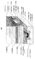
- FIG. 1 is a top view of a semiconductor device according to Example 1 which is the first embodiment of the present invention.
- FIG. 2 is a top view showing a mounting form of the IGBT chip portion in the semiconductor device of FIG.
- FIG. 3 is a top view of the IGBT chip portion in the semiconductor device of FIG. 4 is a cross-sectional view showing a cross-sectional configuration of the semiconductor device taken along line AA ′ of FIG.
- the semiconductor device of this embodiment is an example when applied to an IGBT module.
- a configuration in which a module in which an IGBT chip and a free wheel diode chip are mounted on a collector wiring on a common ceramic substrate is used as a semiconductor device will be described.
- the present invention is limited to this configuration. is not.
- a MOSFET- (Metal-Oxide-Semiconductor-Field-Effect-Transistor) chip is mounted with a freewheel diode chip, or a MOSFET chip body diode is mounted but a freewheel diode chip is not mounted.
- a so-called diode-less configuration used as the configuration those configurations are also included in the technical scope of the present invention.
- the collector wiring 103 on the ceramic substrate, the IGBT chip 105, and the diode chip 106 are bonded to each other by a lower sintered bonding layer (sintered layer) 401 described later in the description of FIG. 4.
- a lower sintered bonding layer (sintered layer) 401 described later in the description of FIG. 4.
- separate conductive members 107 are connected by an upper sintered bonding layer (sintered layer) 401, and the emitter of the IGBT chip 105 and the anode of the Diode chip are bonded to each other. They are connected to each other by wires, and are connected to the ceramic substrate emitter wiring 104 and the ceramic substrate emitter sense wiring 109 by separate bonding wires.
- the sintered layer 401 includes a lower layer and an upper layer, and both are separated from each other.
- the gate electrode pad 204 of the IGBT chip is connected to the gate wiring on the ceramic substrate with a bonding wire.
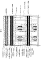
- FIG. 2 is a top view showing the mounting form of the IGBT chip portion in the semiconductor device of the present invention.
- the IGBT chip 105 has an Al field plate 403 and a PWEL 405 for holding the breakdown voltage of the IGBT in a ring shape on the outer periphery of the chip.
- An emitter electrode 205 and a gate electrode pad 204 are formed of a termination region 201 and an element active region inside thereof.
- the conductive member 107 is connected by the sintered bonding layer 301, and the second gate wiring 202 is disposed on the outer periphery of the conductive member 107.
- FIG. 3 is a top view of the IGBT chip before connection of the conductive member.
- a first gate wiring is formed under the emitter electrode, connected to the second gate wiring 202 at the outer periphery, and input from the gate electrode pad. Distribute the generated signal into the IGBT chip.
- FIG. 4 is a cross-sectional view of the semiconductor device when the semiconductor device of the present invention is cut along the line AA ′ of FIG. 1B and FIG. 2, and this figure is also a view showing a cross-section of the gate wiring portion.
- an N buffer layer 408 and a P + collector layer 409 are formed on the back surface of an n-Si substrate 408, a Ni plating electrode 402 is formed on a back electrode 410 (for example, an AlSi / Ti / AlSi laminated structure), It is connected to the collector wiring 101 on the ceramic substrate by a bonding layer (for example, sintered Cu).
- a gate wiring formed on the surface of the IGBT chip is electrically insulated by an insulating oxide film 407 and a PWEL 405 is disposed under the gate wiring in order to maintain a withstand voltage.
- the gate wiring is composed of a first gate wiring 206 and a second gate wiring 202.
- the first gate wiring 206 is made of poly-Si
- the second gate wiring is made of Al
- the first gate wiring 206 is made of Al.
- the gate wiring 206 and the second gate wiring 202 are connected by a contact (for example, Ti / TiN / W) at the outer periphery of the active region.
- An Al field plate 403 and a PWEL 405 are disposed in the outermost peripheral region of the IGBT chip, and this plays a role of maintaining a withstand voltage.
- an emitter electrode 205 for example, an AlSi / Ti / AlSi laminated structure
- a Ni plating electrode 402 is formed in the same manner as the back surface electrode, and is connected to the conductive member 107 by a sintered layer (for example, sintered Cu).
- the emitter electrode, the second gate wiring 202 and the Al field plate 403 are insulated by polyimide 406.
- the conductive member 107 is required to have a role of relaxing thermal stress due to a difference in thermal expansion coefficient between the semiconductor chip and the wiring member and a role of radiating heat from the semiconductor chip. Therefore, it is preferable to use a material having a thermal expansion coefficient intermediate between the semiconductor chip and the wiring member and having a thermal conductivity of 100 W / mK or more as the conductive plate. Further, if a material having a higher thermal conductivity than the direction perpendicular to the electrode surface of the semiconductor chip is used as the conductive member 107, the chip of the conductive plate is formed before the heat generated by the chip is transmitted to the wiring such as the upper wire or ribbon.
- a material in which graphite fiber and metal (copper, aluminum, etc.) having thermal conductivity anisotropy such as 20 W / mK on a certain surface but 2000 W / mK in the orthogonal direction can be used. It is also preferable to use a material in which layers having different thermal conductivities, such as a copper / invar / copper cladding material, are stacked.
- the thermal conductivity of Invar is 13 W / mK, which is less than 400 W / mK for copper, making it difficult for the heat generated in the semiconductor chip to be transmitted to the top, and heat the copper inside along the chip surface. This is because of propagation and soaking.
- the other is the ratio of thermal expansion to Si or SiC (3 to 5 ppm / K) and wiring material (Al about 23 ppm / K) by the ratio of copper (thermal expansion coefficient about 16 ppm / K) and Invar (about 1 ppm / K). This is because it can be adjusted to an intermediate preferable value of about 16 ppm / K), and thermal stress can be reduced.
- the conductive member 107 and the IGBT chip are connected to each other by a sintered layer by a method of applying only a necessary part using a metal mask having an opening of a sintered material application part, a method of applying a necessary part using a dispenser, silicone, Bonding by applying water repellent resin containing fluorine etc. with a metal mask or mesh mask with only the necessary part opened, or applying photosensitive water repellent resin on the substrate or electronic component, exposing and developing After removing the part where the material is applied and applying the bonding paste to the opening, and after applying the water-repellent resin to the substrate or electronic component, the part where the bonding material is applied is removed by the laser and then bonded. For example, there is a method of applying an adhesive paste to the opening. These application methods can be combined according to the area and shape of the electrodes to be joined. In this embodiment, a sintered layer is printed and applied under the conductive member 107 to perform bonding.
- metal particles with a particle size of 100 nm or less are generated from the metal particle precursor during bonding, and metal bonding is performed by fusing metal particles with a particle size of 100 nm or less while discharging organic substances in the bonding layer. It is preferable to apply heat and a pressure of 0.01 to 5 MPa in order to carry out.
- the emitter electrode 205 and the Ni plating 402 disposed on the first gate wiring 206 serve to reduce the generation of cracks in the first gate wiring 206 and the Si substrate due to excessive stress due to pressure when connected to the conductive member 107. .
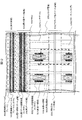
- FIG. 5 is a main part layout diagram of the surface of the IGBT chip portion of the semiconductor device.
- the semiconductor device of this embodiment is a semiconductor device including a so-called trench gate type IGBT chip in which the gate is formed of a trench gate 501 which is a kind of side gate structure, but the present invention is not limited to the trench gate type. . That is, the configuration including the trench gate type IGBT chip is merely an example, and a semiconductor device including a semiconductor chip having another gate structure is also included in the technical scope of the present invention.
- 6 and 7 show bird's-eye views of the areas B and C in FIG. 5, respectively.
- the gate wiring is roughly divided into an active portion gate wiring 504 and an outermost peripheral gate wiring 503.
- a trench gate 501 is arranged so as to be orthogonal to the gate wiring, and a surface n + layer 507, a surface p + layer 508, and a surface p layer 509 are formed between the trench gates.
- the surface n + layer 507 is an electron source source when a gate voltage is applied, and the surface p layer 509 plays a role of determining a threshold voltage when the gate voltage is applied.
- the surface p + layer 508 provides a potential to the surface p layer 509 and serves as a hole current path during IGBT operation.
- the surface p + layer 508 and the surface n + layer 507 are connected to the emitter electrode 205 via the emitter electrode connection contact 506.
- a Ni plating electrode 402 is formed and connected to the conductive member 107 by a sintered layer 401.
- the emitter electrode 205 and the sintered layer 401 are formed on the active portion first gate wiring 206 on which the conductive member 107 is disposed so as to cover it, and the conductive member 107 is disposed thereon.
- the Ni plating electrode 402 is formed on the emitter electrode 205, and the sintered layer 401 is further formed thereon, that is, at least the emitter electrode 205 and the sintered layer 401 as described above.
- a multi-layer structure including two or more layers includes an electrode layer containing Ni as a component (for example, a Ni-plated electrode 402) between the emitter electrode 205 and the sintered layer 401.
- the present invention is not limited to this configuration, and the Ni plating electrode 402 is not an essential component.
- the multi-layer structure described above is not limited to the emitter extraction region (the region where the emitter electrode connection contact 506 is present), but also the emitter electrode connection contact 506 and the gate wiring region (the region where the active portion gate wiring 504 is present and the outermost peripheral gate).
- the wiring 503 is arranged so as to continuously exist over a wide range including a part of the wiring 503.
- the semiconductor device of this embodiment includes the semiconductor chip 105, the first gate wiring 206 and the second gate wiring 202 formed on the surface of the semiconductor chip 105, and the emitter arranged so as to cover the first gate wiring 206.
- a semiconductor device comprising an electrode 205 and a sintered layer 401 disposed above the emitter electrode 205, and a plurality of layers comprising at least the emitter electrode 205 and the sintered layer 401 on the surface of the semiconductor chip 105
- the semiconductor device has a structure that continuously exists over a range including the emitter electrode connection contact 506 and the gate wiring regions 503 and 504. This multi-layer structure mainly serves to protect the gate wiring region from the pressure at the time of sintering joining, and also serves to protect the inside of the Si substrate.
- the first gate wiring 206 can be, for example, a buried trench type gate wiring, but the present invention is not limited to this configuration, and other types of gate wiring such as a non-buried type as shown in FIG. 6 are formed. It may also be configured. In the outermost peripheral gate wiring region, the first gate wiring 206 and the second gate wiring 202 are connected by the outermost peripheral second gate wiring contact 701.
- a polyimide 406 is formed on the second gate wiring to insulate it from the emitter electrode and the terminal Al field plate.
- the gate wiring preferably distributes the signal input from the gate electrode pad within the IGBT chip and distributes the gate signal evenly.
- the gate signal is delayed by a CR time constant determined by the gate wiring resistance and gate capacitance.
- the gate wiring is preferably arranged so that the resistance is reduced by silicidation or the difference in CR time constant due to the divided wiring in the chip is reduced.
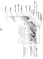
- FIG. 10, and FIG. 11 show a cross-sectional structure of the prior art, a layout of the main part of the IGBT chip surface, and a bird's eye view, respectively.
- the step between the second gate wiring in the active part and the emitter electrode 205 is large. Due to the pressure when connecting the conductive member 107 and the IGBT chip, the pressure is not evenly applied, cracks occur in the second gate wiring 801 and Si, and a short circuit failure occurs between the gate and the emitter as the main electrode. did. With the structure of the present invention, it is possible to reduce the step between the second gate wiring and the emitter electrode 205 in the active part, pressure is applied evenly, and mechanical protection of the gate wiring by the emitter electrode and Ni plating prevents the generation of cracks. It is possible to reduce.
- FIG. 12 is a main part layout diagram of the IGBT chip portion in the semiconductor device according to Example 2 which is the second embodiment of the present invention.
- FIG. 13 is a bird's-eye view of FIG. 12E region. Parts having the same configurations as those of the first embodiment are denoted by the same reference numerals, and description of overlapping portions is omitted.
- the feature of the present embodiment is that the active portion gate wiring 504 is formed by a buried gate wiring 1201 embedded in the trench portion.
- the first embodiment is different from the first embodiment. And in common.
- the buried gate wiring 1201 is formed in the same process as the trench gate 501, and the trench gate 501 and the buried gate wiring 1201 are connected in the trench.
- the pressure at the time of connecting the conductive member 107 and the IGBT chip by the sintered layer is more evenly applied, and the generation of cracks can be reduced by mechanical protection of the emitter electrode and the gate wiring by Ni plating.
- FIG. 14 is a main part layout diagram of a portion of an IGBT chip in a semiconductor device according to Example 3 which is the third embodiment of the present invention.
- FIG. 15 is a bird's-eye view of FIG. 14F region. Parts having the same configurations as those in the first and second embodiments are denoted by the same reference numerals, and description of overlapping portions is omitted.
- the gate is formed of a sidewall gate 1403 which is a kind of side gate structure, and the active internal gate wiring 504 is formed of a buried sidewall gate wiring 1402, and the sidewall gate 1403 It is connected to the.
- the present embodiment is characterized by this point, and is different from the first and second embodiments in that respect, but the other matters are common to the first embodiment.
- the floating p layer 1202 is deleted. As a result, the potential fluctuation of the gate due to the influence of the floating p layer is eliminated, and the controllability of dv / dt is improved. Further, one side of the trench gate 501 is covered with a thick insulating film by the sidewall gate 1403 structure. Thereby, since the feedback capacity is reduced, the controllability of dv / dt is improved.
- a PolySi field plate 1404 connected to the emitter electrode 205 is provided between the sidewall gates 1403 provided in the wide trench 1401. Since the electric field at the corner of the sidewall gate 1403 is relaxed by the PolySi field plate 1404, a withstand voltage is secured.
- the PolySi field plate 1404 alleviates a step caused by providing the wide trench 1401.
- the embedded sidewall gate wiring 1402 can reduce the step between the active portion gate wiring 504 and the emitter electrode 205, and when the conductive member 107 and the IGBT chip are connected by the sintered layer. It is possible to reduce the occurrence of cracks by applying a uniform pressure and applying mechanical protection to the emitter electrode and the gate wiring by Ni plating.
- Example 4 which is an example of an embodiment in which the semiconductor device of the present invention is applied to a power conversion device will be described below.
- FIG. 16 is a circuit block diagram showing a power conversion device 600 that employs the semiconductor device according to the first embodiment of the present invention as a constituent element.
- FIG. 16 shows, as an example of the power conversion apparatus of the present invention, a circuit configuration of a power conversion apparatus 600 according to the present embodiment and a connection relationship between a DC power supply and a three-phase AC motor (AC load).
- AC load three-phase AC motor
- the semiconductor device of the first embodiment is used as the power switching elements 601 to 606.
- the power switching elements 601 to 606 are, for example, IGBTs.
- the power conversion apparatus 600 of the fourth embodiment includes a pair of DC terminals 631, N terminals 632, and U terminals 633, which are AC terminals of the same number as the number of phases of AC output. V terminal 634 and W terminal 635 are provided.
- a switching leg which is composed of a series connection of a pair of power switching elements 601 and 602, and outputs a U terminal 633 connected to the series connection point.
- the power switching elements 603 and 604 having the same configuration are connected in series, and a switching leg having an output of a V terminal 634 connected to the series connection point is provided.
- the power switching elements 605 and 606 having the same configuration are connected in series, and a switching leg having an output of a W terminal 635 connected to the series connection point is provided.
- the power switching elements 601 to 606 are, for example, IGBTs.
- the switching legs for three phases composed of the power switching elements 601 to 606 are connected between the DC terminals of the P terminal 631 and the N terminal 632, and DC power is supplied from a DC power source (not shown).
- a U terminal 633, a V terminal 634, and a W terminal 635, which are three-phase AC terminals of the power converter 600, are connected to a three-phase AC motor (not shown) as a three-phase AC power source.
- the diodes 621 to 626 are connected in antiparallel to the power switching elements 601 to 606, respectively.
- Gate circuits 511 to 516 control the input terminals of the gates of the power switching elements 601 to 606 made of IGBT.
- the power conversion device of this embodiment is a power conversion device that inputs DC power from the outside, converts the input DC power to AC power, and outputs the AC power, and a pair of DC power for inputting DC power.
- AC terminals for output of AC power (631, 632), AC terminals for outputting AC power, and AC terminals (633, 634, 635) of the same number as the number of AC phases related to the AC power.
- the switching element for example, 601 and the switching element are A series circuit (for example, a parallel circuit of 601 and 621) in which two parallel circuits (for example, a parallel circuit of 601 and 621) formed by connecting diodes of opposite polarity (for example 621) in parallel with each other are connected in series , 602 and 622 parallel circuit) and connected directly Interconnection point of the two parallel circuits constituting the circuit, in which further comprising a connected configuration to the AC terminals of the phases corresponding to the series circuit (e.g., U-phase) (e.g. U terminal 633).
- the parallel circuit in this configuration is constituted by the semiconductor device of the present invention (for example, the semiconductor device according to any one of Examples 1 to 3).
- the semiconductor device according to the first embodiment is described as a module in which the IGBT chip and the free wheel diode chip are mounted on the collector wiring on the common ceramic substrate.
- the present invention is limited to the configuration.
- a diode-less configuration is also included in the technical scope of the present invention.
- the switching elements 601, 602, 603, 604, 605, 606 and the diodes 621, 622, 623, 624, 625, 626 in FIG. Needless to say. That is, in the semiconductor device as a module described in the first embodiment in which the IGBT chip and the free wheel diode chip are mounted on the collector wiring on the common ceramic substrate, the switching elements 601, 602, 603, 604, 605 , 606 are constituted by semiconductor chips (for example, IGBT chip 105), and diodes 621, 622, 623, 624, 625, and 626 are arranged on the collector wiring 103 on the common ceramic substrate 101 together with the semiconductor chip 105.
- the power conversion device of the present invention is not limited to this configuration, although the diode chip 106 is joined by the lower sintered layer 401 that is separated from the sintered layer 401.
- gate circuits 611 to 616 are preferably configured to be controlled in an integrated manner by an overall control circuit (not shown).
- the gate circuits 611 to 616 collectively and appropriately control the power switching elements 601 to 606, respectively, so that the DC power of the DC power supply Vcc is converted into three-phase AC power, and the U terminal 633, V terminal 634, W terminal Output from 635.
- the long-term reliability of the power conversion device 600 is improved by applying the semiconductor device according to each of the above embodiments to the power conversion device 600. Also, since no solder is used, it is lead-free and has a good effect on the environment. In addition, long-term reliability can be ensured even if it can be installed in a place with a high temperature environment and does not have a dedicated cooler.
- the semiconductor chip when a metal plate (conductive member) is sintered and bonded onto a semiconductor chip having an IGBT gate structure, the semiconductor chip can be applied even if pressure is applied in the sintering bonding process.
- Semiconductor device with reduced characteristic defects such as short circuit failure between the gate and the main electrode emitter, and main-voltage drop failure between the emitter and collector, in which excessive stress is not easily generated in the gate wiring portion of It becomes possible to provide the used power converter.
- the present invention relates to a bonding layer of an electric bonding portion (for example, a bonding portion between a semiconductor element and a circuit member) in an electronic component, and in particular, bonding using a bonding material mainly composed of copper oxide particles. It is suitable for application to a semiconductor device having a layer.
- the case of the inverter device has been described as an example of application of the semiconductor device of the present invention to the power conversion device.
- the present invention is not limited to this, and the present invention is not limited to this. It can also be applied to other power conversion devices.
Abstract
Provided is a semiconductor device in which, in a case where a metallic plate (a conductive member) is bonded by being sintered to a semiconductor chip having an IGBT gate structure, an excess stress is less likely to be generated in a gate wiring section of the semiconductor chip even when pressure is applied in a sinter bonding process, so that a characteristic failure is reduced. The semiconductor device according to the present invention is characterized by: being provided with a semiconductor chip (105) having a gate structure represented by an IGBT; including first gate wiring (206) and second gate wiring (202) formed on the surface of the semiconductor chip; and including an emitter electrode (205) disposed so as to cover the first gate wiring and a sintered layer disposed above the emitter electrode, wherein a multilayer structure formed by including at least the emitter electrode and the sintered layer on the surface of the semiconductor chip continuously exists over a range including an emitter electrode connecting contact 506 and gate wiring regions 503, 504.
Description
本発明は、電子部品中の電気的接合部(例えば、半導体素子と回路部材との接合部)の接合層に特徴のある半導体装置に関し、特に、焼結接合層を有する半導体装置、およびそれを用いた電力変換装置に関する。
The present invention relates to a semiconductor device characterized by a junction layer of an electrical junction (for example, a junction between a semiconductor element and a circuit member) in an electronic component, and in particular, a semiconductor device having a sintered junction layer and the semiconductor device It is related with the power converter used.
半導体装置は、システムLSI(Large Scale Integration)、電力変換装置、ハイブリッド自動車等の制御装置等、幅広い分野で使用されている。この半導体装置としては、例えば電子部品の電極端子と回路基板上の回路パターンの電極端子との電気的接合に、鉛を含んだ「はんだ」や「はんだ合金」を用いるものがかつては主流であった。
Semiconductor devices are used in a wide range of fields such as system LSI (Large Scale Integration), power conversion devices, control devices for hybrid vehicles, and the like. As this semiconductor device, for example, one that uses “solder” or “solder alloy” containing lead for electrical connection between an electrode terminal of an electronic component and an electrode terminal of a circuit pattern on a circuit board was once the mainstream. It was.
ところが、地球環境保全の観点から鉛の使用が厳しく制限されるようになり、かかる制限の範囲内で鉛を使用する、あるいは鉛を含まない材料で半導体装置の電極等の接合を行なう開発が進められている。特に、「高温はんだ」に関してはその代替となる有効な材料がまだ見出されていない。半導体装置の実装においては「階層はんだ」を用いることが必要不可欠なため、この「高温はんだ」に代わる材料の出現が望まれている。
However, the use of lead has been severely restricted from the viewpoint of global environmental protection, and the development of using lead within the scope of such restriction or joining electrodes of semiconductor devices etc. with materials that do not contain lead has advanced. It has been. In particular, no effective material has yet been found for "high temperature solder". Since it is indispensable to use “hierarchical solder” in the mounting of a semiconductor device, the appearance of a material replacing this “high temperature solder” is desired.
このような背景から、「高温はんだ」に代わる材料として、従来、金属粒子と有機化合物との複合材料を接合材料として用いて電極を接合する接合技術が提案されている。
From such a background, a joining technique for joining electrodes using a composite material of metal particles and an organic compound as a joining material has been proposed as a material to replace “high temperature solder”.
例えば、特許文献1には、ニッケル(以下、「Ni」と表記する)又は銅(以下、「Cu」と表記する)の電極に対して優れた接合強度が得られる接合技術として、酸化第二銅(CuO)粒子と有機物とからなる還元剤を含む接合材料を用いて、還元雰囲気下において接合を行う方法が記載されている。この方法は、加熱還元時に100nm以下の銅粒子を生成させ、銅粒子同士を焼結させて接合する方法である。同文献にはさらに、半導体チップと金属板とを接合する接合材として、焼結性の銀微粒子を含有する材料を用いることが記載されている。
For example, Patent Document 1 discloses a second oxidation technique as a bonding technique that provides excellent bonding strength with respect to an electrode of nickel (hereinafter referred to as “Ni”) or copper (hereinafter referred to as “Cu”). A method is described in which bonding is performed in a reducing atmosphere using a bonding material including a reducing agent composed of copper (CuO) particles and an organic substance. This method is a method in which copper particles of 100 nm or less are generated at the time of heat reduction, and the copper particles are sintered and joined together. The document further describes the use of a material containing sinterable silver fine particles as a bonding material for bonding a semiconductor chip and a metal plate.
また、特許文献2には、配線接続の信頼性を向上させる技術として、配線部材と半導体チップとの中間の熱膨張係数を持つ金属板を用いて、熱膨張係数差の大きな接続部を無くす、応力緩衝の観点からの解決方法が記載されている。
Further, in Patent Document 2, as a technique for improving the reliability of wiring connection, a metal plate having a thermal expansion coefficient intermediate between the wiring member and the semiconductor chip is used, and a connection portion having a large difference in thermal expansion coefficient is eliminated. A solution from the point of view of stress buffering is described.
特許文献1に記載の酸化第二銅(CuO)粒子を用いた接合技術は、従来のナノ粒子接合と比較してNiやCuに対する接合性を改善することができ、Ni電極又はCu電極用の接合材料として期待できる。例えば、電力変換装置のインバータに使用されるIGBT(Insulated Gate Bipolar Transistor)やフリーホイールダイオード等のパワー半導体チップのNi電極に銅焼結層からなる接合層を介して電気的に接続端子に接続することが可能である。
The joining technique using cupric oxide (CuO) particles described in Patent Document 1 can improve the joining property to Ni or Cu as compared with the conventional nanoparticle joining, and can be used for Ni electrodes or Cu electrodes. It can be expected as a bonding material. For example, an IGBT (Insulated Gate Bipolar Transistor) used in an inverter of a power converter or an Ni electrode of a power semiconductor chip such as a free wheel diode is electrically connected to a connection terminal through a bonding layer made of a copper sintered layer. It is possible.
シリコン(以下、「Si」と表記する)や炭化ケイ素(以下、「SiC」と表記する)で構成される半導体チップの主電極は、銅やアルミニウムなどで構成されるワイヤ、リボン等の配線材料で他のチップや電極と接続される。半導体チップの動作温度が高くなると、半導体チップと配線材料とでは熱膨張率に差があるために、スイッチング動作(通電のONとOFFとの切替え動作)を繰り返すうちに、熱疲労で接合部に不具合が生じるという問題があった。
The main electrode of a semiconductor chip composed of silicon (hereinafter referred to as “Si”) or silicon carbide (hereinafter referred to as “SiC”) is a wiring material such as a wire or ribbon composed of copper or aluminum. With other chips and electrodes. When the operating temperature of the semiconductor chip rises, the thermal expansion coefficient differs between the semiconductor chip and the wiring material. There was a problem that a malfunction occurred.
そこで、配線接続の信頼性を向上させる技術として、特許文献2に記載されているように、配線部材と半導体チップとの中間の熱膨張係数の金属板を用いて、熱膨張係数差の大きな接続部を無くす、応力緩衝の観点からの解決方法が提案された。
Therefore, as a technique for improving the reliability of wiring connection, as described in Patent Document 2, a metal plate having a thermal expansion coefficient intermediate between the wiring member and the semiconductor chip is used to connect with a large difference in thermal expansion coefficient. A solution from the point of view of stress buffering has been proposed.
しかしながら、IGBTのようなゲート構造を有する半導体チップ上に金属板(導電部材)を焼結接合する場合、 焼結接合プロセスにおける加圧により、導体チップのゲート配線部に過剰な応力が発生しクラックが生じてしまう課題がある。発生したクラックは、例えばゲートと主電極であるエミッタ間の短絡不良、エミッタとコレクタ間の主耐圧低下不良などを生じてしまう場合があるという問題があった。
However, when a metal plate (conductive member) is sintered and bonded onto a semiconductor chip having a gate structure such as an IGBT, excessive stress is generated in the gate wiring portion of the conductor chip due to pressurization in the sinter bonding process. There is a problem that will occur. For example, the generated crack may cause a short circuit failure between the gate and the emitter, which is the main electrode, and a main breakdown voltage drop failure between the emitter and the collector.
このような事情を鑑みれば、焼結接合プロセスにおける加圧による特性不良を低減できる半導体装置、およびその半導体装置の製造方法、並びにその半導体装置を用いた電力変換装置を提供することが課題となる。
In view of such circumstances, it is an object to provide a semiconductor device capable of reducing characteristic defects due to pressure in a sintering bonding process, a method for manufacturing the semiconductor device, and a power conversion device using the semiconductor device. .
上記課題を解決するために、本発明の半導体装置は、半導体チップと、前記半導体チップの表面に形成された第1ゲート配線および第2ゲート配線と、前記第1ゲート配線を覆うように配置されたエミッタ電極と、前記エミッタ電極の上方に配置された焼結層とを備え、前記半導体チップの表面に、少なくとも前記エミッタ電極と前記焼結層とを含んで成る複数層構造が、エミッタ電極接続コンタクトとゲート配線領域とを含む範囲に亘って連続して存在することを特徴とする。
In order to solve the above problems, a semiconductor device of the present invention is arranged to cover a semiconductor chip, a first gate wiring and a second gate wiring formed on the surface of the semiconductor chip, and the first gate wiring. A multi-layer structure comprising at least the emitter electrode and the sintered layer on the surface of the semiconductor chip, the emitter electrode connected to the emitter electrode, and a sintered layer disposed above the emitter electrode. It exists continuously over the range including the contact and the gate wiring region.
また、本発明の電力変換装置は、外部から直流電力を入力し、入力した前記直流電力を交流電力に変換して出力する電力変換装置であって、前記直流電力を入力するための一対の直流端子と、前記交流電力を出力するための交流端子であって前記交流電力に係る交流の相数と同数の交流端子とを備え、前記相数の前記交流端子の各々について、前記一対の直流端子の一方と他方との間に、スイッチング素子と該スイッチング素子とは逆極性のダイオードとが互いに並列接続されて成る並列回路が2個直列に接続された構成の直列回路が接続され、前記直列回路を構成する2個の前記並列回路の相互接続点が、該直列回路に対応する相の前記交流端子に接続された構成を更に備え、前記並列回路が本発明の半導体装置で構成されることを特徴とする。
The power converter of the present invention is a power converter that inputs DC power from the outside, converts the input DC power into AC power, and outputs the AC power, and a pair of DC power for inputting the DC power. A terminal and an AC terminal for outputting the AC power, the number of AC terminals being the same as the number of AC phases related to the AC power, and the pair of DC terminals for each of the AC terminals of the number of phases A series circuit having a configuration in which two parallel circuits formed by connecting a switching element and a diode having a polarity opposite to that of the switching element are connected in series is connected between one and the other of The interconnection point of the two parallel circuits constituting the circuit further includes a configuration connected to the AC terminal of the phase corresponding to the series circuit, and the parallel circuit is configured by the semiconductor device of the present invention. Characteristic To.
本発明によれば、IGBTのゲート構造を有する半導体チップ上に金属板(導電部材)を焼結接合する際の加圧によってゲート配線部に過剰な応力がかかるのを抑制できると共に、ゲート電極をエミッタ電極で保護できるため、焼結接合プロセス上の加圧を行ってもクラックの発生しにくい、特性不良の低減された半導体装置を提供することができる。
According to the present invention, it is possible to suppress excessive stress from being applied to the gate wiring portion due to pressurization when a metal plate (conductive member) is sintered and bonded onto a semiconductor chip having an IGBT gate structure. Since it can be protected by the emitter electrode, it is possible to provide a semiconductor device with reduced characteristic defects that is unlikely to crack even when pressure is applied during the sintering bonding process.
本発明の半導体装置は、IGBTに代表されるゲート構造を有する半導体チップ(105)を備え、半導体チップ表面に形成された第1ゲート配線(206)および第2ゲート配線(202)を有し、第1ゲート配線を覆うように配置されたエミッタ電極(205)およびエミッタ電極上方に配置された焼結層を有し、半導体チップ表面に少なくともエミッタ電極と焼結層とを含んで成る複数層構造(層数が2以上の層構造)が、エミッタ電極接続コンタクト(506)とゲート配線領域(503、504)とを含む範囲に亘って連続して存在することを特徴とする。
The semiconductor device of the present invention includes a semiconductor chip (105) having a gate structure represented by IGBT, and has a first gate wiring (206) and a second gate wiring (202) formed on the surface of the semiconductor chip, A multi-layer structure having an emitter electrode (205) disposed so as to cover the first gate wiring and a sintered layer disposed above the emitter electrode, and including at least the emitter electrode and the sintered layer on the surface of the semiconductor chip (A layer structure having two or more layers) continuously exists over a range including the emitter electrode connection contact (506) and the gate wiring regions (503, 504).
本発明の上記の構成において、さらに、アクティブ部内ゲート配線(504)とエミッタ電極(205)との段差を低減する構成としてもよい。これにより、導電部材(107)とIGBTチップとを焼結層によって互いに接続する際の圧力の偏りを低減することが可能となる。
In the above-described configuration of the present invention, a step between the active internal gate wiring (504) and the emitter electrode (205) may be further reduced. As a result, it is possible to reduce the pressure bias when the conductive member (107) and the IGBT chip are connected to each other by the sintered layer.
また、本発明の上記の構成において、さらに、ゲート配線をエミッタ電極及びNiメッキによって機械的に保護する構成としてもよい。これにより、クラック発生を低減することが可能となる。
In the above-described configuration of the present invention, the gate wiring may be further mechanically protected by the emitter electrode and Ni plating. Thereby, crack generation can be reduced.
以下、本発明の実施形態について図面を参照して詳細に説明する。
Hereinafter, embodiments of the present invention will be described in detail with reference to the drawings.
各図において、参照番号が同一のものは同一の構成要件あるいは類似の機能を備えた構成要件を示している。また、p-、p、p+は、半導体層の導電型がp型であることを示し、かつこの順に相対的な不純物濃度が高くなる。さらに、n-、n、n+は、半導体層の導電型がn型であることを示し、かつこの順に相対的な不純物濃度が高くなる。
In each figure, components having the same reference number indicate the same configuration requirements or configuration requirements having similar functions. P−, p, and p + indicate that the conductivity type of the semiconductor layer is p-type, and the relative impurity concentration increases in this order. Further, n−, n, and n + indicate that the conductivity type of the semiconductor layer is n-type, and the relative impurity concentration increases in this order.
(実施例1)
図1は、本発明の第1の実施形態である実施例1に係る半導体装置の上面図である。また、図2は、図1の半導体装置におけるIGBTチップの部分の実装形態を示す上面図である。また、図3は、図1の半導体装置におけるIGBTチップの部分の上面図である。また、図4は、図1のA-A’線における半導体装置の断面の構成を示す断面図である。 Example 1
FIG. 1 is a top view of a semiconductor device according to Example 1 which is the first embodiment of the present invention. FIG. 2 is a top view showing a mounting form of the IGBT chip portion in the semiconductor device of FIG. FIG. 3 is a top view of the IGBT chip portion in the semiconductor device of FIG. 4 is a cross-sectional view showing a cross-sectional configuration of the semiconductor device taken along line AA ′ of FIG.
本実施例の半導体装置は、IGBTモジュールに適用した場合の例である。なお、本例では、IGBTチップとフリーホイールダイオードチップとが共通のセラミック基板上のコレクタ配線上に実装されたモジュールを半導体装置とした構成について説明するが、本発明はこの構成に限定されるものではない。例えば、MOSFET (Metal-Oxide-Semiconductor Field-Effect Transistor) チップをフリーホイールダイオードチップと共に実装した構成、あるいは、MOSFETチップは実装するがフリーホイールダイオードチップは実装せずにMOSFETチップのボディダイオードを還流ダイオードとして使用する、いわゆるダイオードレスの構成においても同様に、本発明の技術思想は適用可能であるため、それらの構成も本発明の技術的範囲に含まれる。
The semiconductor device of this embodiment is an example when applied to an IGBT module. In this example, a configuration in which a module in which an IGBT chip and a free wheel diode chip are mounted on a collector wiring on a common ceramic substrate is used as a semiconductor device will be described. However, the present invention is limited to this configuration. is not. For example, a MOSFET- (Metal-Oxide-Semiconductor-Field-Effect-Transistor) chip is mounted with a freewheel diode chip, or a MOSFET chip body diode is mounted but a freewheel diode chip is not mounted. Similarly, since the technical idea of the present invention can be applied to a so-called diode-less configuration used as the configuration, those configurations are also included in the technical scope of the present invention.
セラミック基板101上にセラミック基板上コレクタ配線103とIGBTチップ105及びDiodeチップ106とが、図4の説明において後述する下側の焼結接合層(焼結層)401で互いに接合されている。IGBTチップ105及びDiodeチップ106の上方には、それぞれ別々の導電部材107が上側の焼結接合層(焼結層)401で接続されており、IGBTチップ105のエミッタとDiodeチップのアノードとはボンディングワイヤーで互いに接続されると共に、セラミック基板上エミッタ配線104及びセラミック基板上エミッタセンス配線109にそれぞれ別々のボンディングワイヤーで接続されている。焼結層401は、上記のように、下側の層と上側の層とを含んで構成され、また、この両者は互いに分離している。
On the ceramic substrate 101, the collector wiring 103 on the ceramic substrate, the IGBT chip 105, and the diode chip 106 are bonded to each other by a lower sintered bonding layer (sintered layer) 401 described later in the description of FIG. 4. Above the IGBT chip 105 and the Diode chip 106, separate conductive members 107 are connected by an upper sintered bonding layer (sintered layer) 401, and the emitter of the IGBT chip 105 and the anode of the Diode chip are bonded to each other. They are connected to each other by wires, and are connected to the ceramic substrate emitter wiring 104 and the ceramic substrate emitter sense wiring 109 by separate bonding wires. As described above, the sintered layer 401 includes a lower layer and an upper layer, and both are separated from each other.
また、IGBTチップのゲート電極パッド204は、セラミック基板上ゲート配線にボンディングワイヤーで接続されている。
The gate electrode pad 204 of the IGBT chip is connected to the gate wiring on the ceramic substrate with a bonding wire.
図2は、本発明の半導体装置におけるIGBTチップの部分の実装形態を示す上面図であり、IGBTチップ105は、IGBTの耐圧を保持するためのAlフィールドプレート403及びPWEL405がチップ外周にリング状に配置された終端領域201とその内側の素子アクティブ領域とから成り、エミッタ電極205及びゲート電極パッド204が形成れている。エミッタ電極上には、導電部材107が焼結接合層301により接続され、導電部材107の外周部に第2ゲート配線202が配置されている。
FIG. 2 is a top view showing the mounting form of the IGBT chip portion in the semiconductor device of the present invention. The IGBT chip 105 has an Al field plate 403 and a PWEL 405 for holding the breakdown voltage of the IGBT in a ring shape on the outer periphery of the chip. An emitter electrode 205 and a gate electrode pad 204 are formed of a termination region 201 and an element active region inside thereof. On the emitter electrode, the conductive member 107 is connected by the sintered bonding layer 301, and the second gate wiring 202 is disposed on the outer periphery of the conductive member 107.
図3は、導電部材接続前のIGBTチップの上面図であり、エミッタ電極下には、第1ゲート配線が形成されており、外周部で第2ゲート配線202に接続され、ゲート電極パッドより入力された信号をIGBTチップ内に分配する。
FIG. 3 is a top view of the IGBT chip before connection of the conductive member. A first gate wiring is formed under the emitter electrode, connected to the second gate wiring 202 at the outer periphery, and input from the gate electrode pad. Distribute the generated signal into the IGBT chip.
図4は、図1 、図2のA-A’線で本発明の半導体装置を切断した場合における半導体装置の断面図であり、同図はゲート配線部の断面を示す図にもなっている。IGBTチップは、n-Si基板408の裏面にNバッファー層408及びP+コレクタ層409が形成されており、裏面電極410(例えばAlSi/Ti/AlSi積層構造)にNiメッキ電極402が形成され、焼結層(例えば焼結Cu)でセラミック基板上コレクタ配線101に接続されている。IGBTチップの表面に形成されるゲート配線は、絶縁酸化膜407で電気的に絶縁され耐圧を保持するために、ゲート配線下には、PWEL405が配置されている。ゲート配線は、第1のゲート配線206と第2のゲート配線202からなり、例えば第1のゲート配線206はポリSiで形成され、第2のゲート配線はAlで形成されており、 第1のゲート配線206と第2のゲート配線202はアクティブ領域の外周部でコンタクト(例えば、Ti/TiN/W)で接続されている。IGBTチップ最外周領域には、Alフィールドプレート403及びPWEL405が配置され、これは耐圧を保持する役割を果たす。アクティブ領域には、エミッタ電極205(例えばAlSi/Ti/AlSi積層構造)が配置され、裏面電極同様にNiメッキ電極402が形成され、焼結層(例えば焼結Cu)で導電部材107と接続されている。エミッタ電極、第2のゲート配線202及びAlフィールドプレート403は、ポリイミド406により絶縁されている。ここで、導電部材107は、半導体チップと配線部材との熱膨張率差による熱応力を緩和する役割と、半導体チップからの熱を放熱する役割とが求められる。したがって、導電板としては、半導体チップと配線部材との中間の熱膨張率を有し、熱伝導率が100W/mK以上の材料を用いることが好ましい。さらに導電部材107として、半導体チップの電極面に水平な方向が垂直な方向より熱伝導率が高い材料を用いれば、チップの発熱が上部のワイヤやリボンなどの配線に伝わる前に導電板のチップ面に沿った面内で熱が拡散し、良好な均熱効果が得られるため、チップの特定部分だけが高温になってワイヤもしくはリボンが剥がれることが無くなり、チップ全体として配線接続信頼性が向上する。例えば、ある面で20W/mKだが、その直交方向には2000W/mKである、といった熱伝導異方性を有するグラファイト繊維と金属(銅、アルミニウムなど)を複合化した材料を用いることができる。また、銅/インバー/銅のクラッド材料など、異なる熱伝導率を有する層を積層した材料を用いることが好ましい。これは、一つにはインバー(鉄ニッケル合金)の熱伝導率が13W/mKと銅の400W/mKよりも小さいため半導体チップの発熱を上部に伝えにくく、チップ面に沿って銅内部を熱が伝播し均熱化されるためである。もう一つには、銅(熱膨張率約16ppm/K)とインバー(約1ppm/K)の比率によって熱膨張率をSiやSiC(3~5ppm/K)と配線部材(Al約23ppm/K、Cu約16ppm/K)の中間の好ましい値に調整することが可能であり、熱応力を低減できるためである。
4 is a cross-sectional view of the semiconductor device when the semiconductor device of the present invention is cut along the line AA ′ of FIG. 1B and FIG. 2, and this figure is also a view showing a cross-section of the gate wiring portion. . In the IGBT chip, an N buffer layer 408 and a P + collector layer 409 are formed on the back surface of an n-Si substrate 408, a Ni plating electrode 402 is formed on a back electrode 410 (for example, an AlSi / Ti / AlSi laminated structure), It is connected to the collector wiring 101 on the ceramic substrate by a bonding layer (for example, sintered Cu). A gate wiring formed on the surface of the IGBT chip is electrically insulated by an insulating oxide film 407 and a PWEL 405 is disposed under the gate wiring in order to maintain a withstand voltage. The gate wiring is composed of a first gate wiring 206 and a second gate wiring 202. For example, the first gate wiring 206 is made of poly-Si, the second gate wiring is made of Al, and the first gate wiring 206 is made of Al. The gate wiring 206 and the second gate wiring 202 are connected by a contact (for example, Ti / TiN / W) at the outer periphery of the active region. An Al field plate 403 and a PWEL 405 are disposed in the outermost peripheral region of the IGBT chip, and this plays a role of maintaining a withstand voltage. In the active region, an emitter electrode 205 (for example, an AlSi / Ti / AlSi laminated structure) is disposed, a Ni plating electrode 402 is formed in the same manner as the back surface electrode, and is connected to the conductive member 107 by a sintered layer (for example, sintered Cu). ing. The emitter electrode, the second gate wiring 202 and the Al field plate 403 are insulated by polyimide 406. Here, the conductive member 107 is required to have a role of relaxing thermal stress due to a difference in thermal expansion coefficient between the semiconductor chip and the wiring member and a role of radiating heat from the semiconductor chip. Therefore, it is preferable to use a material having a thermal expansion coefficient intermediate between the semiconductor chip and the wiring member and having a thermal conductivity of 100 W / mK or more as the conductive plate. Further, if a material having a higher thermal conductivity than the direction perpendicular to the electrode surface of the semiconductor chip is used as the conductive member 107, the chip of the conductive plate is formed before the heat generated by the chip is transmitted to the wiring such as the upper wire or ribbon. Since heat is diffused in the plane along the plane and a good soaking effect is obtained, only a specific part of the chip becomes hot and the wire or ribbon does not peel off, improving the wiring connection reliability as a whole chip To do. For example, a material in which graphite fiber and metal (copper, aluminum, etc.) having thermal conductivity anisotropy such as 20 W / mK on a certain surface but 2000 W / mK in the orthogonal direction can be used. It is also preferable to use a material in which layers having different thermal conductivities, such as a copper / invar / copper cladding material, are stacked. This is because, in part, the thermal conductivity of Invar (iron-nickel alloy) is 13 W / mK, which is less than 400 W / mK for copper, making it difficult for the heat generated in the semiconductor chip to be transmitted to the top, and heat the copper inside along the chip surface. This is because of propagation and soaking. The other is the ratio of thermal expansion to Si or SiC (3 to 5 ppm / K) and wiring material (Al about 23 ppm / K) by the ratio of copper (thermal expansion coefficient about 16 ppm / K) and Invar (about 1 ppm / K). This is because it can be adjusted to an intermediate preferable value of about 16 ppm / K), and thermal stress can be reduced.
導電部材107とIGBTチップとの焼結層による接続は、焼結材塗布部分を開口したメタルマスクを用いて必要部分にのみ塗布を行う方法、ディスペンサを用いて必要部分に塗布する方法、シリコーンやフッ素等を含む撥水性の樹脂を必要な部分のみ開口したメタルマスクやメッシュ状マスクで塗布したり、感光性のある撥水性樹脂を基板あるいは電子部品上に塗布し、露光および現像することにより接合材料を塗布する部分を除去し、接合用ペーストをその開口部に塗布する方法や、さらには撥水性樹脂を基板あるいは電子部品に塗布後、接合材料を塗布する部分をレーザーにより除去した後、接合用ペーストをその開口部に塗布する方法などがある。これらの塗布方法は、接合する電極の面積、形状に応じて組み合わせ可能である。本実施例では、導電部材107の下に焼結層を印刷塗布し接合を行っている。
The conductive member 107 and the IGBT chip are connected to each other by a sintered layer by a method of applying only a necessary part using a metal mask having an opening of a sintered material application part, a method of applying a necessary part using a dispenser, silicone, Bonding by applying water repellent resin containing fluorine etc. with a metal mask or mesh mask with only the necessary part opened, or applying photosensitive water repellent resin on the substrate or electronic component, exposing and developing After removing the part where the material is applied and applying the bonding paste to the opening, and after applying the water-repellent resin to the substrate or electronic component, the part where the bonding material is applied is removed by the laser and then bonded. For example, there is a method of applying an adhesive paste to the opening. These application methods can be combined according to the area and shape of the electrodes to be joined. In this embodiment, a sintered layer is printed and applied under the conductive member 107 to perform bonding.
本接合材料を用いた接合では、接合時に金属粒子前駆体から粒径が100nm以下の金属粒子を生成し、接合層における有機物を排出しながら粒径が100nm以下の金属粒子の融着による金属結合を行うために熱と0.01~5MPaの圧力を加えることが好ましい。第1ゲート配線206上に配置されたエミッタ電極205及びNiメッキ402は、導電部材107と接続する際の圧力による過剰応力による第1ゲート配線206及びSi基板内のクラック発生を低減させる役割を果たす。
In bonding using this bonding material, metal particles with a particle size of 100 nm or less are generated from the metal particle precursor during bonding, and metal bonding is performed by fusing metal particles with a particle size of 100 nm or less while discharging organic substances in the bonding layer. It is preferable to apply heat and a pressure of 0.01 to 5 MPa in order to carry out. The emitter electrode 205 and the Ni plating 402 disposed on the first gate wiring 206 serve to reduce the generation of cracks in the first gate wiring 206 and the Si substrate due to excessive stress due to pressure when connected to the conductive member 107. .
次に、ゲート配線領域とエミッタ電極領域の関係を詳細に説明する。
Next, the relationship between the gate wiring region and the emitter electrode region will be described in detail.
図5は、半導体装置のIGBTチップの部分の表面の要部レイアウト図である。本実施例の半導体装置は、ゲートがサイドゲート構造の一種であるトレンチゲート501で形成される、いわゆるトレンチゲート型のIGBTチップを備えた半導体装置であるが、本発明はトレンチゲート型に限定されない。つまり、トレンチゲート型のIGBTチップを備えた構成はあくまでも一例であって、他のゲート構造を有する半導体チップを備えた半導体装置も本発明の技術的範囲に含まれる。また、図6及び図7に、図5におけるB領域及びC領域の鳥瞰図をそれぞれ示す。ゲート配線は、アクティブ部内ゲート配線504と最外周ゲート配線503とに大別される。
FIG. 5 is a main part layout diagram of the surface of the IGBT chip portion of the semiconductor device. The semiconductor device of this embodiment is a semiconductor device including a so-called trench gate type IGBT chip in which the gate is formed of a trench gate 501 which is a kind of side gate structure, but the present invention is not limited to the trench gate type. . That is, the configuration including the trench gate type IGBT chip is merely an example, and a semiconductor device including a semiconductor chip having another gate structure is also included in the technical scope of the present invention. 6 and 7 show bird's-eye views of the areas B and C in FIG. 5, respectively. The gate wiring is roughly divided into an active portion gate wiring 504 and an outermost peripheral gate wiring 503.
各ゲート配線間には、トレンチゲート501がゲート配線直交するように配置され、トレンチゲート間には、表面n+層507、表面p+層508、表面p層509が形成されている。表面n+層507は、ゲート電圧が印加された際の電子のソース源であり、表面p層509はゲート電圧印加時のしきい値電圧を決定する役割を果たす。表面p+層508は、表面p層509に電位を与えると共にIGBT動作時のホール電流経路となる。表面p+層508及び表面n+層507は、エミッ電極接続コンタクト506を介して、エミッタ電極205に接続される。エミッタ電極上には、Niメッキ電極402が形成され、焼結層401によって導電部材107と接続されている。ここで、導電部材107が配置されるアクティブ部内第1ゲート配線206上には、それを覆うように少なくともエミッタ電極205及び焼結層401が形成され、その上に導電部材107が配置される。特に本実施例においては、エミッタ電極205の上にNiメッキ電極402が形成され、さらにその上に焼結層401が形成される構成、すなわち、上記のように少なくともエミッタ電極205及び焼結層401を含んで成る複数層構造(すなわち層数が2以上である層構造)が、エミッタ電極205と焼結層401との間にNiを含有成分とする電極層(例えばNiメッキ電極402)を備えた構成としているが、本発明はこの構成に限定されず、Niメッキ電極402は必須構成要素ではない。また、上記の複数層構造は、エミッタ引出し領域(エミッタ電極接続コンタクト506の在る領域)のみならず、エミッタ電極接続コンタクト506とゲート配線領域(アクティブ部内ゲート配線504の在る領域および最外周ゲート配線503の一部の在る領域)とを含む広い範囲に亘って連続して存在するように配置される。つまり、本実施例の半導体装置は、半導体チップ105と、半導体チップ105の表面に形成された第1ゲート配線206および第2ゲート配線202と、第1ゲート配線206を覆うように配置されたエミッタ電極205と、エミッタ電極205の上方に配置された焼結層401とを備えた半導体装置であると共に、半導体チップ105の表面に、少なくともエミッタ電極205と焼結層401とを含んで成る複数層構造が、エミッタ電極接続コンタクト506とゲート配線領域503、504とを含む範囲に亘って連続して存在する半導体装置である。この複数層構造は、焼結接合時の圧力から主にゲート配線領域を保護する役割を果たし、ひいてはSi基板内を保護する役割をも果たす。
Between each gate wiring, a trench gate 501 is arranged so as to be orthogonal to the gate wiring, and a surface n + layer 507, a surface p + layer 508, and a surface p layer 509 are formed between the trench gates. The surface n + layer 507 is an electron source source when a gate voltage is applied, and the surface p layer 509 plays a role of determining a threshold voltage when the gate voltage is applied. The surface p + layer 508 provides a potential to the surface p layer 509 and serves as a hole current path during IGBT operation. The surface p + layer 508 and the surface n + layer 507 are connected to the emitter electrode 205 via the emitter electrode connection contact 506. On the emitter electrode, a Ni plating electrode 402 is formed and connected to the conductive member 107 by a sintered layer 401. Here, at least the emitter electrode 205 and the sintered layer 401 are formed on the active portion first gate wiring 206 on which the conductive member 107 is disposed so as to cover it, and the conductive member 107 is disposed thereon. In particular, in this embodiment, the Ni plating electrode 402 is formed on the emitter electrode 205, and the sintered layer 401 is further formed thereon, that is, at least the emitter electrode 205 and the sintered layer 401 as described above. A multi-layer structure including two or more layers (that is, a layer structure having two or more layers) includes an electrode layer containing Ni as a component (for example, a Ni-plated electrode 402) between the emitter electrode 205 and the sintered layer 401. However, the present invention is not limited to this configuration, and the Ni plating electrode 402 is not an essential component. In addition, the multi-layer structure described above is not limited to the emitter extraction region (the region where the emitter electrode connection contact 506 is present), but also the emitter electrode connection contact 506 and the gate wiring region (the region where the active portion gate wiring 504 is present and the outermost peripheral gate). The wiring 503 is arranged so as to continuously exist over a wide range including a part of the wiring 503. That is, the semiconductor device of this embodiment includes the semiconductor chip 105, the first gate wiring 206 and the second gate wiring 202 formed on the surface of the semiconductor chip 105, and the emitter arranged so as to cover the first gate wiring 206. A semiconductor device comprising an electrode 205 and a sintered layer 401 disposed above the emitter electrode 205, and a plurality of layers comprising at least the emitter electrode 205 and the sintered layer 401 on the surface of the semiconductor chip 105 The semiconductor device has a structure that continuously exists over a range including the emitter electrode connection contact 506 and the gate wiring regions 503 and 504. This multi-layer structure mainly serves to protect the gate wiring region from the pressure at the time of sintering joining, and also serves to protect the inside of the Si substrate.
第1ゲート配線206は、例えば埋め込みトレンチ型のゲート配線とすることができるが、本発明はこの構成に限定されず、図6に示すような非埋め込み型など、他の型のゲート配線が形成された構成でもよい。また、最外周ゲート配線領域は、第1ゲート配線206と第2ゲート配線202とが最外周第2ゲート配線コンタクト701で接続されている。
The first gate wiring 206 can be, for example, a buried trench type gate wiring, but the present invention is not limited to this configuration, and other types of gate wiring such as a non-buried type as shown in FIG. 6 are formed. It may also be configured. In the outermost peripheral gate wiring region, the first gate wiring 206 and the second gate wiring 202 are connected by the outermost peripheral second gate wiring contact 701.
第2ゲート配線上には、エミッタ電極及び終端部Alフィールドプレートと絶縁するためのポリイミド406が形成されている。ゲート配線は、ゲート電極パッドより入力された信号をIGBTチップ内に分配し、ゲート信号を均等に分配することが好ましい。ゲート信号は、ゲート配線抵抗及びゲート容量で決まるCR時定数により遅延を発生させる。ゲート配線は好ましくは、シリサイド化による低抵抗化またはチップ内分割配線によるCR時定数の差が小さくなるように配置することが好ましい。図9、図10、及び図11に、従来技術の断面構造、IGBTチップ表面の要部レイアウト、及び鳥瞰図をそれぞれ示す。アクティブ部内第1のゲート配線206上にアクティブ部内第2ゲート配線コンタクト1002を介して、アクティブ部内に第2ゲート配線801を設けた場合、アクティブ部内の第2ゲート配線とエミッタ電極205の段差が大きく、導電部材107とIGBTチップを接続する際の圧力により、圧力が均等にかからず、第2ゲート配線801及びSi内部にクラックが発生し、ゲートと主電極であるエミッタ間の短絡不良が発生した。本発明構造により、アクティブ部内の第2ゲート配線とエミッタ電極205の段差を小さくすることが可能であり圧力が均等に掛かり、かつエミッタ電極及びNiメッキによるゲート配線の機械的保護により、クラック発生を低減することが可能である。
A polyimide 406 is formed on the second gate wiring to insulate it from the emitter electrode and the terminal Al field plate. The gate wiring preferably distributes the signal input from the gate electrode pad within the IGBT chip and distributes the gate signal evenly. The gate signal is delayed by a CR time constant determined by the gate wiring resistance and gate capacitance. The gate wiring is preferably arranged so that the resistance is reduced by silicidation or the difference in CR time constant due to the divided wiring in the chip is reduced. 9, FIG. 10, and FIG. 11 show a cross-sectional structure of the prior art, a layout of the main part of the IGBT chip surface, and a bird's eye view, respectively. When the second gate wiring 801 is provided in the active part on the first gate wiring 206 in the active part via the second gate wiring contact 1002 in the active part, the step between the second gate wiring in the active part and the emitter electrode 205 is large. Due to the pressure when connecting the conductive member 107 and the IGBT chip, the pressure is not evenly applied, cracks occur in the second gate wiring 801 and Si, and a short circuit failure occurs between the gate and the emitter as the main electrode. did. With the structure of the present invention, it is possible to reduce the step between the second gate wiring and the emitter electrode 205 in the active part, pressure is applied evenly, and mechanical protection of the gate wiring by the emitter electrode and Ni plating prevents the generation of cracks. It is possible to reduce.
(実施例2)
図12は、本発明の第2の実施形態である実施例2に係る半導体装置におけるIGBTチップの部分の要部レイアウト図である。また、図13は図12 E領域の鳥瞰図である。実施例1と同一構成の部分には同一符号を付して重複箇所の説明を省略する。 (Example 2)
FIG. 12 is a main part layout diagram of the IGBT chip portion in the semiconductor device according to Example 2 which is the second embodiment of the present invention. FIG. 13 is a bird's-eye view of FIG. 12E region. Parts having the same configurations as those of the first embodiment are denoted by the same reference numerals, and description of overlapping portions is omitted.
本実施例の特徴は、アクティブ部内ゲート配線504がトレンチ部分に埋め込まれた埋め込みゲート配線1201で形成されている点にあり、その点で実施例1とは異なるが、その他の事項は実施例1と共通である。埋め込みゲート配線1201は、トレンチゲート501と同一工程で形成され、トレンチゲート501及び埋め込みゲート配線1201は、トレンチ内で接続されている。実施例1に比べて、アクティブ部内ゲート配線504とエミッタ電極205の段差を更に低減することが可能である。導電部材107とIGBTチップを焼結層による接続する際の圧力が更に均等にかかり、かつエミッタ電極及びNiメッキによるゲート配線の機械的保護により、クラック発生を低減することが可能である。
The feature of the present embodiment is that the active portion gate wiring 504 is formed by a buried gate wiring 1201 embedded in the trench portion. In this respect, the first embodiment is different from the first embodiment. And in common. The buried gate wiring 1201 is formed in the same process as the trench gate 501, and the trench gate 501 and the buried gate wiring 1201 are connected in the trench. Compared with the first embodiment, it is possible to further reduce the level difference between the active part gate wiring 504 and the emitter electrode 205. The pressure at the time of connecting the conductive member 107 and the IGBT chip by the sintered layer is more evenly applied, and the generation of cracks can be reduced by mechanical protection of the emitter electrode and the gate wiring by Ni plating.
(実施例3)
図14は、本発明の第3の実施形態である実施例3に係る半導体装置におけるIGBTチップの部分の要部レイアウト図である。また、図15は図14 F領域の鳥瞰図である。実施例1および実施例2と同一構成の部分には同一符号を付して重複箇所の説明を省略する。 (Example 3)
FIG. 14 is a main part layout diagram of a portion of an IGBT chip in a semiconductor device according to Example 3 which is the third embodiment of the present invention. FIG. 15 is a bird's-eye view of FIG. 14F region. Parts having the same configurations as those in the first and second embodiments are denoted by the same reference numerals, and description of overlapping portions is omitted.
本実施例の半導体装置においては、ゲートがサイドゲート構造の一種であるサイドウォールゲート1403で形成されており、アクティブ部内ゲート配線504は、埋め込みサイドウォール型ゲート配線1402で形成され、サイドウォールゲート1403に接続されている。本実施例はこの点を特徴としており、また、その点で実施例1および実施例2とは異なるが、その他の事項は実施例1と共通である。
In the semiconductor device of this embodiment, the gate is formed of a sidewall gate 1403 which is a kind of side gate structure, and the active internal gate wiring 504 is formed of a buried sidewall gate wiring 1402, and the sidewall gate 1403 It is connected to the. The present embodiment is characterized by this point, and is different from the first and second embodiments in that respect, but the other matters are common to the first embodiment.
幅広いトレンチ1401を設けることで、フローティングp層1202が削除される。これにより、フローティングp層の影響によるゲートの電位変動が無くなり、dv/dtの制御性が向上する。さらに、サイドウォールゲート1403構造によりトレンチゲート501の片側が厚い絶縁膜で覆われている。これにより、帰還容量が低減するので、dv/dtの制御性が向上する。幅広トレンチ1401内に設けられるサイドウォールゲート1403の間に、エミッタ電極205に接続されるPolySiフィールドプレート1404が設けられる。PolySiフィールドプレート1404によりサイドウォールゲート1403のコーナ部における電界が緩和されるので、耐圧が確保される。また、PolySiフィールドプレート1404により、幅広トレンチ1401を設けることによって生じる段差が緩和される。実施例2と同様に、埋め込みサイドウォール型ゲート配線1402により、アクティブ部内ゲート配線504とエミッタ電極205の段差を低減することが可能であり、導電部材107とIGBTチップを焼結層による接続する際の圧力が更に均等にかかり、かつエミッタ電極及びNiメッキによるゲート配線の機械的保護により、クラック発生を低減することが可能である。
By providing a wide trench 1401, the floating p layer 1202 is deleted. As a result, the potential fluctuation of the gate due to the influence of the floating p layer is eliminated, and the controllability of dv / dt is improved. Further, one side of the trench gate 501 is covered with a thick insulating film by the sidewall gate 1403 structure. Thereby, since the feedback capacity is reduced, the controllability of dv / dt is improved. A PolySi field plate 1404 connected to the emitter electrode 205 is provided between the sidewall gates 1403 provided in the wide trench 1401. Since the electric field at the corner of the sidewall gate 1403 is relaxed by the PolySi field plate 1404, a withstand voltage is secured. Further, the PolySi field plate 1404 alleviates a step caused by providing the wide trench 1401. As in the second embodiment, the embedded sidewall gate wiring 1402 can reduce the step between the active portion gate wiring 504 and the emitter electrode 205, and when the conductive member 107 and the IGBT chip are connected by the sintered layer. It is possible to reduce the occurrence of cracks by applying a uniform pressure and applying mechanical protection to the emitter electrode and the gate wiring by Ni plating.
(実施例4)
本発明の半導体装置を電力変換装置に適用した実施形態の一例である実施例4について、以下、説明する。 Example 4
Example 4 which is an example of an embodiment in which the semiconductor device of the present invention is applied to a power conversion device will be described below.
本発明の半導体装置を電力変換装置に適用した実施形態の一例である実施例4について、以下、説明する。 Example 4
Example 4 which is an example of an embodiment in which the semiconductor device of the present invention is applied to a power conversion device will be described below.
図16は、本発明の実施例1に係る半導体装置を構成要素として採用した電力変換装置600を示す回路ブロック図である。図16は、本発明の電力変換装置の一例として、本実施例に係る電力変換装置600の回路構成、及び直流電源と三相交流モータ(交流負荷)との接続の関係を示す。
FIG. 16 is a circuit block diagram showing a power conversion device 600 that employs the semiconductor device according to the first embodiment of the present invention as a constituent element. FIG. 16 shows, as an example of the power conversion apparatus of the present invention, a circuit configuration of a power conversion apparatus 600 according to the present embodiment and a connection relationship between a DC power supply and a three-phase AC motor (AC load).
本実施例の電力変換装置600では、第1の実施形態の半導体装置を電力スイッチング素子601~606として用いている。電力スイッチング素子601~606は、例えばIGBTである。
In the power conversion device 600 of this example, the semiconductor device of the first embodiment is used as the power switching elements 601 to 606. The power switching elements 601 to 606 are, for example, IGBTs.
図16に示すように、第4の実施形態の電力変換装置600は、一対の直流端子であるP端子631、N端子632と、交流出力の相数と同数の交流端子であるU端子633、V端子634、W端子635とを備えている。
As shown in FIG. 16, the power conversion apparatus 600 of the fourth embodiment includes a pair of DC terminals 631, N terminals 632, and U terminals 633, which are AC terminals of the same number as the number of phases of AC output. V terminal 634 and W terminal 635 are provided.
また、一対の電力スイッチング素子601および602の直列接続からなり、その直列接続点に接続されるU端子633を出力とするスイッチングレッグを備える。また、それと同じ構成の電力スイッチング素子603および604の直列接続からなり、その直列接続点に接続されるV端子634を出力とするスイッチングレッグを備える。また、それと同じ構成の電力スイッチング素子605および606の直列接続からなり、その直列接続点に接続されるW端子635を出力とするスイッチングレッグを備える。
Also, a switching leg is provided which is composed of a series connection of a pair of power switching elements 601 and 602, and outputs a U terminal 633 connected to the series connection point. The power switching elements 603 and 604 having the same configuration are connected in series, and a switching leg having an output of a V terminal 634 connected to the series connection point is provided. The power switching elements 605 and 606 having the same configuration are connected in series, and a switching leg having an output of a W terminal 635 connected to the series connection point is provided.
電力スイッチング素子601~606は、例えばIGBTである。
The power switching elements 601 to 606 are, for example, IGBTs.
電力スイッチング素子601~606からなる3相分のスイッチングレッグは、P端子631、N端子632の直流端子間に接続されて、図示しない直流電源から直流電力が供給される。電力変換装置600の3相の交流端子であるU端子633、V端子634、W端子635は図示しない三相交流モータに三相交流電源として接続されている。
The switching legs for three phases composed of the power switching elements 601 to 606 are connected between the DC terminals of the P terminal 631 and the N terminal 632, and DC power is supplied from a DC power source (not shown). A U terminal 633, a V terminal 634, and a W terminal 635, which are three-phase AC terminals of the power converter 600, are connected to a three-phase AC motor (not shown) as a three-phase AC power source.
電力スイッチング素子601~606には、それぞれ逆並列にダイオード621~626が接続されている。IGBTからなる電力スイッチング素子601~606のそれぞれのゲートの入力端子には、ゲート回路511~516によって制御される。
The diodes 621 to 626 are connected in antiparallel to the power switching elements 601 to 606, respectively. Gate circuits 511 to 516 control the input terminals of the gates of the power switching elements 601 to 606 made of IGBT.
つまり、本実施例の電力変換装置は、外部から直流電力を入力し、入力した前記直流電力を交流電力に変換して出力する電力変換装置であって、直流電力を入力するための一対の直流端子(631、632)と、交流電力を出力するための交流端子であってその交流電力に係る交流の相数と同数の交流端子(633、634、635)とを備え、相数分ある交流端子(633、634、635)の各々について、一対の直流端子(631、632)の一方(P端子)と他方(N端子)との間に、スイッチング素子(例えば601)と該スイッチング素子とは逆極性のダイオード(例えば621)とが互いに並列接続されて成る並列回路(例えば601と621との並列回路)が2個直列に接続された構成の直列回路(例えば601と621との並列回路と、602と622との並列回路との直列回路)が接続され、その直列回路を構成する2個の並列回路の相互接続点が、該直列回路に対応する相(例えばU相)の交流端子(例えばU端子633)に接続された構成を更に備えたものである。また、この構成における並列回路は、本発明の半導体装置(例えば実施例1~3のいずれかに係る半導体装置)で構成される。
That is, the power conversion device of this embodiment is a power conversion device that inputs DC power from the outside, converts the input DC power to AC power, and outputs the AC power, and a pair of DC power for inputting DC power. AC terminals for output of AC power (631, 632), AC terminals for outputting AC power, and AC terminals (633, 634, 635) of the same number as the number of AC phases related to the AC power. For each of the terminals (633, 634, 635), between one (P terminal) and the other (N terminal) of the pair of DC terminals (631, 632), the switching element (for example, 601) and the switching element are A series circuit (for example, a parallel circuit of 601 and 621) in which two parallel circuits (for example, a parallel circuit of 601 and 621) formed by connecting diodes of opposite polarity (for example 621) in parallel with each other are connected in series , 602 and 622 parallel circuit) and connected directly Interconnection point of the two parallel circuits constituting the circuit, in which further comprising a connected configuration to the AC terminals of the phases corresponding to the series circuit (e.g., U-phase) (e.g. U terminal 633). Further, the parallel circuit in this configuration is constituted by the semiconductor device of the present invention (for example, the semiconductor device according to any one of Examples 1 to 3).
上述したように、実施例1の半導体装置は、IGBTチップとフリーホイールダイオードチップとが共通のセラミック基板上のコレクタ配線上に実装されたモジュールとして説明されているが、本発明はその構成に限定されるものではなく、例えば、MOSFETチップをフリーホイールダイオードチップと共に実装した構成、あるいは、MOSFETチップは実装するがフリーホイールダイオードチップは実装せずにMOSFETチップのボディダイオードを還流ダイオードとして使用する、いわゆるダイオードレスの構成も、本発明の技術的範囲に含まれる。このことから明らかではあるが、図16におけるスイッチング素子601、602、603、604、605、606とダイオード621、622、623、624、625、626との関係についてもそれと同様のことが当てはまることは言うまでもない。つまり、実施例1で説明した、IGBTチップとフリーホイールダイオードチップとが共通のセラミック基板上のコレクタ配線上に実装されたモジュールとしての半導体装置においては、スイッチング素子601、602、603、604、605、606は半導体チップ(例えばIGBTチップ105)で構成され、また、ダイオード621、622、623、624、625、626は、共通のセラミック基板101上のコレクタ配線103に、半導体チップ105と共に、上側の焼結層401とは分離している下側の焼結層401で接合されているダイオードチップ106で構成されるが、本発明の電力変換装置はこの構成に限定されない。
As described above, the semiconductor device according to the first embodiment is described as a module in which the IGBT chip and the free wheel diode chip are mounted on the collector wiring on the common ceramic substrate. However, the present invention is limited to the configuration. For example, a configuration in which a MOSFET chip is mounted together with a free wheel diode chip, or a MOSFET chip body diode is mounted but a free wheel diode chip is not mounted, and the MOSFET chip body diode is used as a freewheeling diode. A diode-less configuration is also included in the technical scope of the present invention. As is clear from this, the same applies to the relationship between the switching elements 601, 602, 603, 604, 605, 606 and the diodes 621, 622, 623, 624, 625, 626 in FIG. Needless to say. That is, in the semiconductor device as a module described in the first embodiment in which the IGBT chip and the free wheel diode chip are mounted on the collector wiring on the common ceramic substrate, the switching elements 601, 602, 603, 604, 605 , 606 are constituted by semiconductor chips (for example, IGBT chip 105), and diodes 621, 622, 623, 624, 625, and 626 are arranged on the collector wiring 103 on the common ceramic substrate 101 together with the semiconductor chip 105. The power conversion device of the present invention is not limited to this configuration, although the diode chip 106 is joined by the lower sintered layer 401 that is separated from the sintered layer 401.
なお、ゲート回路611~616は統括制御回路(不図示)によって統括的に制御されるように構成するのが好適である。
Note that the gate circuits 611 to 616 are preferably configured to be controlled in an integrated manner by an overall control circuit (not shown).
ゲート回路611~616によって、それぞれ電力スイッチング素子601~606を統括的に適切に制御して、直流電源Vccの直流電力は、三相交流電力に変換され、U端子633、V端子634、W端子635から出力される。
The gate circuits 611 to 616 collectively and appropriately control the power switching elements 601 to 606, respectively, so that the DC power of the DC power supply Vcc is converted into three-phase AC power, and the U terminal 633, V terminal 634, W terminal Output from 635.
上記各実施形態に係る半導体装置を電力変換装置600に適用することで、電力変換装置600の長期信頼性が向上する。また、半田を用いないので鉛フリーであり、環境に良い効果がある。また、高温環境の場所に搭載でき、かつ専用の冷却器を持たなくても長期的な信頼性を確保することが可能になる。
The long-term reliability of the power conversion device 600 is improved by applying the semiconductor device according to each of the above embodiments to the power conversion device 600. Also, since no solder is used, it is lead-free and has a good effect on the environment. In addition, long-term reliability can be ensured even if it can be installed in a place with a high temperature environment and does not have a dedicated cooler.
以上、本発明の上記各実施例によれば、IGBTのゲート構造を有する半導体チップ上に金属板(導電部材)を焼結接合する際に、焼結接合プロセスにおける加圧を行っても半導体チップのゲート配線部に過剰な応力が発生しにくい、ゲートと主電極であるエミッタとの間の短絡不良やエミッタ-コレクタ間の主耐圧低下不良などの特性不良が低減された半導体装置、およびそれを用いた電力変換装置を提供することが可能となる。
As described above, according to each of the embodiments of the present invention, when a metal plate (conductive member) is sintered and bonded onto a semiconductor chip having an IGBT gate structure, the semiconductor chip can be applied even if pressure is applied in the sintering bonding process. Semiconductor device with reduced characteristic defects such as short circuit failure between the gate and the main electrode emitter, and main-voltage drop failure between the emitter and collector, in which excessive stress is not easily generated in the gate wiring portion of It becomes possible to provide the used power converter.
よって、本発明は、電子部品中の電気的接合部(例えば、半導体素子と回路部材との接合部)の接合層に関し、特に、酸化銅粒子を主材とする接合材を用いて接合した接合層を有する半導体装置に適用して好適である。
Therefore, the present invention relates to a bonding layer of an electric bonding portion (for example, a bonding portion between a semiconductor element and a circuit member) in an electronic component, and in particular, bonding using a bonding material mainly composed of copper oxide particles. It is suitable for application to a semiconductor device having a layer.
なお、本実施形態では、本発明の半導体装置の電力変換装置への適用例として、インバータ装置の場合について説明したが、これに限定されるものではなく、直流-直流コンバータや、交流-直流コンバータなど、他の電力変換装置に適用することもできる。
In the present embodiment, the case of the inverter device has been described as an example of application of the semiconductor device of the present invention to the power conversion device. However, the present invention is not limited to this, and the present invention is not limited to this. It can also be applied to other power conversion devices.
101 セラミック基板
102 セラミック基板上ゲート配線
103 セラミック基板上コレクタ配線
104 セラミック基板上エミッタ配線
105 IGBTチップ
106 Diodeチップ
107 導電部材
108 ボンディングワイヤー
109 セラミック基板上エミッタセンス配線
201 終端領域
202 第2ゲート配線
204 第2ゲート電極パッド
205 エミッタ電極
206 第1ゲート配線
401 焼結層
402 Niメッキ電極
403 終端部Alフィールドプレート
404 コンタクト
405 PWEL
406 ポリイミド
407 絶縁酸化膜
408 N-Si基板
409 P+コレクタ層
410 裏面コレクタ電極
411 Nバッファー層
501 トレンチゲート
502 終端部Alフィールドプレートコンタクト
503 最外周ゲート配線
504 アクティブ部内ゲート配線
505 第2ゲート配線接続コンタクト
506 エミッタ電極接続コンタクト
507 表面n+領域
508 表面p+領域
509 表面p領域
510 ゲート酸化膜
701 最外周第2ゲート配線コンタクト
801 アクティブ部内第2ゲート配線
1002 アクティブ部内第2ゲート配線コンタクト
1201 埋め込みゲート配線
1401 幅広トレンチ領域
1402 埋め込みゲート配線
1403 サイドウォールゲート
1404 PolySiフィールドプレート
1405 PolySiフィールドプレート上エミッタコンタクト
600 電力変換装置
601~606 電力スイッチング素子
621~626 ダイオード
611~616 ゲート回路 101Ceramic substrate 102 Gate wiring on ceramic substrate 103 Collector wiring on ceramic substrate 104 Emitter wiring on ceramic substrate 105 IGBT chip 106 Diode chip 107 Conductive member 108 Bonding wire 109 Emitter sense wiring on ceramic substrate 201 Termination region 202 Second gate wiring 204 Second 2 Gate electrode pad 205 Emitter electrode 206 1st gate wiring 401 Sintered layer 402 Ni plating electrode 403 Termination part Al field plate 404 Contact 405 PWEL
406 Polyimide 407 Insulating oxide film 408 N-Si substrate 409 P + collector layer 410 Back collector electrode 411 N buffer layer 501 Trench gate 502 Terminal Al field plate contact 503 Outermost gate wiring 504 Active part gate wiring 505 Second gate wiring connection contact 506 Emitter electrode contact 507 Surface n + region 508 Surface p + region 509 Surface p region 510 Gate oxide film 701 Outermost second gate wiring contact 801 Active second gate wiring 1002 Active second gate wiring contact 1201 Embedded gate wiring 1401 Wide Trench region 1402 Embedded gate wiring 1403 Sidewall gate 1404 PolySi field plate 1405 Emitter contact onPolySi field plate 600 Power converter 601 to 606 Power switching element 621 to 626 Diode 611 to 616 Gate circuit
102 セラミック基板上ゲート配線
103 セラミック基板上コレクタ配線
104 セラミック基板上エミッタ配線
105 IGBTチップ
106 Diodeチップ
107 導電部材
108 ボンディングワイヤー
109 セラミック基板上エミッタセンス配線
201 終端領域
202 第2ゲート配線
204 第2ゲート電極パッド
205 エミッタ電極
206 第1ゲート配線
401 焼結層
402 Niメッキ電極
403 終端部Alフィールドプレート
404 コンタクト
405 PWEL
406 ポリイミド
407 絶縁酸化膜
408 N-Si基板
409 P+コレクタ層
410 裏面コレクタ電極
411 Nバッファー層
501 トレンチゲート
502 終端部Alフィールドプレートコンタクト
503 最外周ゲート配線
504 アクティブ部内ゲート配線
505 第2ゲート配線接続コンタクト
506 エミッタ電極接続コンタクト
507 表面n+領域
508 表面p+領域
509 表面p領域
510 ゲート酸化膜
701 最外周第2ゲート配線コンタクト
801 アクティブ部内第2ゲート配線
1002 アクティブ部内第2ゲート配線コンタクト
1201 埋め込みゲート配線
1401 幅広トレンチ領域
1402 埋め込みゲート配線
1403 サイドウォールゲート
1404 PolySiフィールドプレート
1405 PolySiフィールドプレート上エミッタコンタクト
600 電力変換装置
601~606 電力スイッチング素子
621~626 ダイオード
611~616 ゲート回路 101
406 Polyimide 407 Insulating oxide film 408 N-Si substrate 409 P + collector layer 410 Back collector electrode 411 N buffer layer 501 Trench gate 502 Terminal Al field plate contact 503 Outermost gate wiring 504 Active part gate wiring 505 Second gate wiring connection contact 506 Emitter electrode contact 507 Surface n + region 508 Surface p + region 509 Surface p region 510 Gate oxide film 701 Outermost second gate wiring contact 801 Active second gate wiring 1002 Active second gate wiring contact 1201 Embedded gate wiring 1401 Wide Trench region 1402 Embedded gate wiring 1403 Sidewall gate 1404 PolySi field plate 1405 Emitter contact on
Claims (10)
- 半導体チップと、
前記半導体チップの表面に形成された第1ゲート配線および第2ゲート配線と、
前記第1ゲート配線を覆うように配置されたエミッタ電極と、
前記エミッタ電極の上方に配置された焼結層と
を備え、
前記半導体チップの表面に、少なくとも前記エミッタ電極と前記焼結層とを含んで成る複数層構造が、エミッタ電極接続コンタクトとゲート配線領域とを含む範囲に亘って連続して存在する
ことを特徴とする半導体装置。 A semiconductor chip;
A first gate wiring and a second gate wiring formed on the surface of the semiconductor chip;
An emitter electrode disposed to cover the first gate wiring;
A sintered layer disposed above the emitter electrode,
A multi-layer structure including at least the emitter electrode and the sintered layer is continuously provided on the surface of the semiconductor chip over a range including an emitter electrode connection contact and a gate wiring region. Semiconductor device. - 請求項1に記載の半導体装置において、
前記複数層構造は、前記エミッタ電極と前記焼結層との間にニッケル(Ni)を含有成分とする電極層を備えて構成される
ことを特徴とする半導体装置。 The semiconductor device according to claim 1,
The multi-layer structure is configured by including an electrode layer containing nickel (Ni) as a component between the emitter electrode and the sintered layer. - 請求項1に記載の半導体装置において、
前記半導体チップは、サイドゲート構造を有するゲートを備えて構成される
ことを特徴とする半導体装置。 The semiconductor device according to claim 1,
The semiconductor device comprises a gate having a side gate structure. - 請求項3に記載の半導体装置において、
前記サイドゲート構造は、前記ゲートがトレンチゲートであるトレンチゲート構造である
ことを特徴とする半導体装置。 The semiconductor device according to claim 3.
The semiconductor device according to claim 1, wherein the side gate structure is a trench gate structure in which the gate is a trench gate. - 請求項4に記載の半導体装置において、
前記第1ゲート配線は、前記トレンチゲートに接続されたトレンチ埋め込み型ゲート配線である
ことを特徴とする半導体装置。 The semiconductor device according to claim 4,
The semiconductor device according to claim 1, wherein the first gate wiring is a trench buried type gate wiring connected to the trench gate. - 請求項3に記載の半導体装置において、
前記サイドゲート構造は、前記ゲートがサイドウォールゲートであるサイドウォールゲート構造である
ことを特徴とする半導体装置。 The semiconductor device according to claim 3.
The semiconductor device according to claim 1, wherein the side gate structure is a sidewall gate structure in which the gate is a sidewall gate. - 請求項6に記載の半導体装置において、
前記第1ゲート配線は、前記サイドウォールゲートに接続された埋め込みサイドウォール型ゲート配線である
ことを特徴とする半導体装置。 The semiconductor device according to claim 6.
The semiconductor device according to claim 1, wherein the first gate wiring is a buried sidewall gate wiring connected to the sidewall gate. - 請求項1乃至7のいずれか一項に記載の半導体装置において、
前記半導体チップは、共通のセラミック基板上のコレクタ配線に、ダイオードチップと共に、前記焼結層とは分離している他の焼結層で接合されている
ことを特徴とする半導体装置。 The semiconductor device according to any one of claims 1 to 7,
The semiconductor device, wherein the semiconductor chip is bonded to a collector wiring on a common ceramic substrate together with a diode chip by another sintered layer separated from the sintered layer. - 外部から直流電力を入力し、入力した前記直流電力を交流電力に変換して出力する電力変換装置であって、
前記直流電力を入力するための一対の直流端子と、
前記交流電力を出力するための交流端子であって前記交流電力に係る交流の相数と同数の交流端子と
を備え、
前記相数の前記交流端子の各々について、前記一対の直流端子の一方と他方との間に、スイッチング素子と該スイッチング素子とは逆極性のダイオードとが互いに並列接続されて成る並列回路が2個直列に接続された構成の直列回路が接続され、前記直列回路を構成する2個の前記並列回路の相互接続点が、該直列回路に対応する相の前記交流端子に接続された構成を更に備え、
前記並列回路が請求項1乃至7のいずれか一項に記載の半導体装置で構成される
ことを特徴とする電力変換装置。 A power converter that inputs DC power from outside, converts the input DC power into AC power, and outputs the AC power,
A pair of DC terminals for inputting the DC power;
An AC terminal for outputting the AC power, comprising the same number of AC terminals as the number of AC phases related to the AC power,
For each of the AC terminals of the number of phases, two parallel circuits are formed by connecting a switching element and a diode having a polarity opposite to that of the switching element in parallel between one and the other of the pair of DC terminals. A series circuit having a configuration connected in series is connected, and an interconnection point of the two parallel circuits constituting the series circuit is further connected to the AC terminal of a phase corresponding to the series circuit. ,
The power converter according to claim 1, wherein the parallel circuit includes the semiconductor device according to claim 1. - 請求項9に記載の電力変換装置において、
前記スイッチング素子は、前記半導体チップで構成され、
前記ダイオードは、共通のセラミック基板上のコレクタ配線に、前記半導体チップと共に、前記焼結層とは分離している他の焼結層で接合されているダイオードチップで構成される
ことを特徴とする電力変換装置。 The power conversion device according to claim 9, wherein
The switching element is composed of the semiconductor chip,
The diode is composed of a diode chip joined to a collector wiring on a common ceramic substrate together with the semiconductor chip and another sintered layer separated from the sintered layer. Power conversion device.
Priority Applications (3)
| Application Number | Priority Date | Filing Date | Title |
|---|---|---|---|
| CN201780083838.3A CN110192284B (en) | 2017-01-19 | 2017-12-25 | Semiconductor device and power conversion device |
| EP17892804.0A EP3573107A4 (en) | 2017-01-19 | 2017-12-25 | Semiconductor device and power conversion apparatus |
| US16/465,429 US10763346B2 (en) | 2017-01-19 | 2017-12-25 | Semiconductor device and power conversion apparatus |
Applications Claiming Priority (2)
| Application Number | Priority Date | Filing Date | Title |
|---|---|---|---|
| JP2017-007161 | 2017-01-19 | ||
| JP2017007161A JP6726112B2 (en) | 2017-01-19 | 2017-01-19 | Semiconductor device and power converter |
Publications (1)
| Publication Number | Publication Date |
|---|---|
| WO2018135239A1 true WO2018135239A1 (en) | 2018-07-26 |
Family
ID=62908444
Family Applications (1)
| Application Number | Title | Priority Date | Filing Date |
|---|---|---|---|
| PCT/JP2017/046299 WO2018135239A1 (en) | 2017-01-19 | 2017-12-25 | Semiconductor device and power conversion apparatus |
Country Status (6)
| Country | Link |
|---|---|
| US (1) | US10763346B2 (en) |
| EP (1) | EP3573107A4 (en) |
| JP (1) | JP6726112B2 (en) |
| CN (1) | CN110192284B (en) |
| TW (1) | TWI638461B (en) |
| WO (1) | WO2018135239A1 (en) |
Cited By (3)
| Publication number | Priority date | Publication date | Assignee | Title |
|---|---|---|---|---|
| CN110867485A (en) * | 2018-08-28 | 2020-03-06 | 株式会社日立功率半导体 | Semiconductor device and power conversion device |
| WO2021064221A1 (en) * | 2019-10-03 | 2021-04-08 | Mqsemi Ag | Semiconductor device and method for producing same |
| JP7428019B2 (en) | 2020-03-06 | 2024-02-06 | 富士電機株式会社 | semiconductor module |
Families Citing this family (3)
| Publication number | Priority date | Publication date | Assignee | Title |
|---|---|---|---|---|
| JP7390984B2 (en) | 2020-06-03 | 2023-12-04 | 三菱電機株式会社 | semiconductor equipment |
| WO2022249803A1 (en) * | 2021-05-27 | 2022-12-01 | 株式会社デンソー | Semiconductor device |
| JP2024044822A (en) * | 2022-09-21 | 2024-04-02 | 株式会社デンソー | Semiconductor Device |
Citations (9)
| Publication number | Priority date | Publication date | Assignee | Title |
|---|---|---|---|---|
| JPH1093086A (en) * | 1996-09-17 | 1998-04-10 | Toyota Central Res & Dev Lab Inc | Insulated-gate type semiconductor device and manufacturing method thereof |
| JPH10303228A (en) * | 1997-04-23 | 1998-11-13 | Hitachi Ltd | Compressively bonded semiconductor device |
| JP2008244242A (en) | 2007-03-28 | 2008-10-09 | Hitachi Ltd | Semiconductor device and its manufacturing method, and composite metallic body and its manufacturing method |
| JP2011049393A (en) * | 2009-08-27 | 2011-03-10 | Mitsubishi Electric Corp | Semiconductor device and method of manufacturing the same |
| JP2012028674A (en) | 2010-07-27 | 2012-02-09 | Mitsubishi Electric Corp | Semiconductor device and semiconductor device manufacturing method |
| JP2012146810A (en) * | 2011-01-12 | 2012-08-02 | Hitachi Ltd | Semiconductor device and electric power conversion apparatus |
| JP2012191238A (en) * | 2012-06-15 | 2012-10-04 | Hitachi Ltd | Conductive sintered layer forming composition, and conductive coating film forming method and jointing method using the same |
| JP2015230932A (en) * | 2014-06-04 | 2015-12-21 | 三菱電機株式会社 | Silicon carbide semiconductor device and silicon carbide semiconductor device manufacturing method |
| JP2016012582A (en) * | 2014-06-27 | 2016-01-21 | 株式会社日立製作所 | Semiconductor device and power conversion equipment using the same |
Family Cites Families (13)
| Publication number | Priority date | Publication date | Assignee | Title |
|---|---|---|---|---|
| US6838722B2 (en) * | 2002-03-22 | 2005-01-04 | Siliconix Incorporated | Structures of and methods of fabricating trench-gated MIS devices |
| JP2004111885A (en) * | 2002-07-23 | 2004-04-08 | Toshiba Corp | Semiconductor device |
| JP5151150B2 (en) | 2006-12-28 | 2013-02-27 | 株式会社日立製作所 | Composition for forming conductive sintered layer, and method for forming conductive film and bonding method using the same |
| JP2010050189A (en) * | 2008-08-20 | 2010-03-04 | Hitachi Metals Ltd | Bonding material, semiconductor device, and method of manufacturing the same |
| JP5611537B2 (en) | 2009-04-28 | 2014-10-22 | 日立化成株式会社 | Conductive bonding material, bonding method using the same, and semiconductor device bonded thereby |
| JP5600698B2 (en) * | 2012-03-14 | 2014-10-01 | 株式会社 日立パワーデバイス | Power semiconductor module with SiC element |
| TWI642154B (en) | 2013-12-25 | 2018-11-21 | 日商三菱綜合材料股份有限公司 | Power module substrate, and method of producing the same; and power module |
| JP2015142059A (en) * | 2014-01-30 | 2015-08-03 | 株式会社日立製作所 | power semiconductor module |
| US9613843B2 (en) | 2014-10-13 | 2017-04-04 | General Electric Company | Power overlay structure having wirebonds and method of manufacturing same |
| JP2016115698A (en) * | 2014-12-11 | 2016-06-23 | トヨタ自動車株式会社 | Semiconductor device and method of manufacturing the same |
| US10109549B2 (en) * | 2014-12-24 | 2018-10-23 | Hitachi, Ltd. | Semiconductor device and power conversion device using same |
| JP6300236B2 (en) * | 2015-02-26 | 2018-03-28 | 株式会社日立製作所 | SEMICONDUCTOR DEVICE, SEMICONDUCTOR DEVICE MANUFACTURING METHOD, AND POWER CONVERSION DEVICE |
| KR101745776B1 (en) | 2015-05-12 | 2017-06-28 | 매그나칩 반도체 유한회사 | Power Semiconductor Device |
-
2017
- 2017-01-19 JP JP2017007161A patent/JP6726112B2/en active Active
- 2017-12-25 EP EP17892804.0A patent/EP3573107A4/en active Pending
- 2017-12-25 WO PCT/JP2017/046299 patent/WO2018135239A1/en unknown
- 2017-12-25 US US16/465,429 patent/US10763346B2/en active Active
- 2017-12-25 CN CN201780083838.3A patent/CN110192284B/en active Active
-
2018
- 2018-01-18 TW TW107101766A patent/TWI638461B/en active
Patent Citations (9)
| Publication number | Priority date | Publication date | Assignee | Title |
|---|---|---|---|---|
| JPH1093086A (en) * | 1996-09-17 | 1998-04-10 | Toyota Central Res & Dev Lab Inc | Insulated-gate type semiconductor device and manufacturing method thereof |
| JPH10303228A (en) * | 1997-04-23 | 1998-11-13 | Hitachi Ltd | Compressively bonded semiconductor device |
| JP2008244242A (en) | 2007-03-28 | 2008-10-09 | Hitachi Ltd | Semiconductor device and its manufacturing method, and composite metallic body and its manufacturing method |
| JP2011049393A (en) * | 2009-08-27 | 2011-03-10 | Mitsubishi Electric Corp | Semiconductor device and method of manufacturing the same |
| JP2012028674A (en) | 2010-07-27 | 2012-02-09 | Mitsubishi Electric Corp | Semiconductor device and semiconductor device manufacturing method |
| JP2012146810A (en) * | 2011-01-12 | 2012-08-02 | Hitachi Ltd | Semiconductor device and electric power conversion apparatus |
| JP2012191238A (en) * | 2012-06-15 | 2012-10-04 | Hitachi Ltd | Conductive sintered layer forming composition, and conductive coating film forming method and jointing method using the same |
| JP2015230932A (en) * | 2014-06-04 | 2015-12-21 | 三菱電機株式会社 | Silicon carbide semiconductor device and silicon carbide semiconductor device manufacturing method |
| JP2016012582A (en) * | 2014-06-27 | 2016-01-21 | 株式会社日立製作所 | Semiconductor device and power conversion equipment using the same |
Non-Patent Citations (1)
| Title |
|---|
| See also references of EP3573107A4 |
Cited By (4)
| Publication number | Priority date | Publication date | Assignee | Title |
|---|---|---|---|---|
| CN110867485A (en) * | 2018-08-28 | 2020-03-06 | 株式会社日立功率半导体 | Semiconductor device and power conversion device |
| CN110867485B (en) * | 2018-08-28 | 2023-09-26 | 株式会社日立功率半导体 | Semiconductor device and power conversion device |
| WO2021064221A1 (en) * | 2019-10-03 | 2021-04-08 | Mqsemi Ag | Semiconductor device and method for producing same |
| JP7428019B2 (en) | 2020-03-06 | 2024-02-06 | 富士電機株式会社 | semiconductor module |
Also Published As
| Publication number | Publication date |
|---|---|
| TWI638461B (en) | 2018-10-11 |
| CN110192284B (en) | 2022-06-03 |
| JP6726112B2 (en) | 2020-07-22 |
| EP3573107A1 (en) | 2019-11-27 |
| CN110192284A (en) | 2019-08-30 |
| US20200006301A1 (en) | 2020-01-02 |
| US10763346B2 (en) | 2020-09-01 |
| TW201828480A (en) | 2018-08-01 |
| EP3573107A4 (en) | 2020-07-01 |
| JP2018117054A (en) | 2018-07-26 |
Similar Documents
| Publication | Publication Date | Title |
|---|---|---|
| WO2018135239A1 (en) | Semiconductor device and power conversion apparatus | |
| US10056319B2 (en) | Power module package having patterned insulation metal substrate | |
| US10483216B2 (en) | Power module and fabrication method for the same | |
| JP6300236B2 (en) | SEMICONDUCTOR DEVICE, SEMICONDUCTOR DEVICE MANUFACTURING METHOD, AND POWER CONVERSION DEVICE | |
| TWI556388B (en) | Embedded packaging device | |
| US20120175755A1 (en) | Semiconductor device including a heat spreader | |
| CN108735692B (en) | Semiconductor device with a semiconductor device having a plurality of semiconductor chips | |
| US10727209B2 (en) | Semiconductor device and semiconductor element with improved yield | |
| JP2020077723A (en) | Semiconductor device | |
| US20130112993A1 (en) | Semiconductor device and wiring substrate | |
| JP5054755B2 (en) | Semiconductor device | |
| CN109727932B (en) | Power semiconductor module | |
| CN114008775A (en) | Semiconductor device and method for manufacturing the same | |
| WO2021200166A1 (en) | Semiconductor device | |
| JP2015026667A (en) | Semiconductor module | |
| JP7419781B2 (en) | semiconductor module | |
| JP6906583B2 (en) | Semiconductor power module | |
| US20190258302A1 (en) | Power supply module | |
| US9991191B2 (en) | Electronic power device with flat electronic interconnection structure | |
| US9362221B2 (en) | Surface mountable power components | |
| JP7294403B2 (en) | semiconductor equipment | |
| US20230028808A1 (en) | Semiconductor device | |
| WO2021200138A1 (en) | Semiconductor device | |
| JP7004233B2 (en) | Semiconductor device | |
| JP2022188994A (en) | Semiconductor device |
Legal Events
| Date | Code | Title | Description |
|---|---|---|---|
| 121 | Ep: the epo has been informed by wipo that ep was designated in this application |
Ref document number: 17892804 Country of ref document: EP Kind code of ref document: A1 |
|
| NENP | Non-entry into the national phase |
Ref country code: DE |
|
| ENP | Entry into the national phase |
Ref document number: 2017892804 Country of ref document: EP Effective date: 20190819 |