WO2023223588A1 - 半導体チップ - Google Patents
半導体チップ Download PDFInfo
- Publication number
- WO2023223588A1 WO2023223588A1 PCT/JP2022/046591 JP2022046591W WO2023223588A1 WO 2023223588 A1 WO2023223588 A1 WO 2023223588A1 JP 2022046591 W JP2022046591 W JP 2022046591W WO 2023223588 A1 WO2023223588 A1 WO 2023223588A1
- Authority
- WO
- WIPO (PCT)
- Prior art keywords
- region
- semiconductor
- semiconductor chip
- electric field
- contact
- Prior art date
- Legal status (The legal status is an assumption and is not a legal conclusion. Google has not performed a legal analysis and makes no representation as to the accuracy of the status listed.)
- Ceased
Links
Images



Classifications
-
- H—ELECTRICITY
- H10—SEMICONDUCTOR DEVICES; ELECTRIC SOLID-STATE DEVICES NOT OTHERWISE PROVIDED FOR
- H10D—INORGANIC ELECTRIC SEMICONDUCTOR DEVICES
- H10D62/00—Semiconductor bodies, or regions thereof, of devices having potential barriers
- H10D62/10—Shapes, relative sizes or dispositions of the regions of the semiconductor bodies; Shapes of the semiconductor bodies
- H10D62/13—Semiconductor regions connected to electrodes carrying current to be rectified, amplified or switched, e.g. source or drain regions
- H10D62/149—Source or drain regions of field-effect devices
- H10D62/151—Source or drain regions of field-effect devices of IGFETs
- H10D62/156—Drain regions of DMOS transistors
- H10D62/157—Impurity concentrations or distributions
-
- H—ELECTRICITY
- H10—SEMICONDUCTOR DEVICES; ELECTRIC SOLID-STATE DEVICES NOT OTHERWISE PROVIDED FOR
- H10D—INORGANIC ELECTRIC SEMICONDUCTOR DEVICES
- H10D30/00—Field-effect transistors [FET]
- H10D30/60—Insulated-gate field-effect transistors [IGFET]
- H10D30/64—Double-diffused metal-oxide semiconductor [DMOS] FETs
- H10D30/66—Vertical DMOS [VDMOS] FETs
- H10D30/668—Vertical DMOS [VDMOS] FETs having trench gate electrodes, e.g. UMOS transistors
-
- H—ELECTRICITY
- H10—SEMICONDUCTOR DEVICES; ELECTRIC SOLID-STATE DEVICES NOT OTHERWISE PROVIDED FOR
- H10D—INORGANIC ELECTRIC SEMICONDUCTOR DEVICES
- H10D62/00—Semiconductor bodies, or regions thereof, of devices having potential barriers
- H10D62/10—Shapes, relative sizes or dispositions of the regions of the semiconductor bodies; Shapes of the semiconductor bodies
- H10D62/102—Constructional design considerations for preventing surface leakage or controlling electric field concentration
- H10D62/103—Constructional design considerations for preventing surface leakage or controlling electric field concentration for increasing or controlling the breakdown voltage of reverse-biased devices
- H10D62/105—Constructional design considerations for preventing surface leakage or controlling electric field concentration for increasing or controlling the breakdown voltage of reverse-biased devices by having particular doping profiles, shapes or arrangements of PN junctions; by having supplementary regions, e.g. junction termination extension [JTE]
- H10D62/106—Constructional design considerations for preventing surface leakage or controlling electric field concentration for increasing or controlling the breakdown voltage of reverse-biased devices by having particular doping profiles, shapes or arrangements of PN junctions; by having supplementary regions, e.g. junction termination extension [JTE] having supplementary regions doped oppositely to or in rectifying contact with regions of the semiconductor bodies, e.g. guard rings with PN or Schottky junctions
- H10D62/107—Buried supplementary regions, e.g. buried guard rings
-
- H—ELECTRICITY
- H10—SEMICONDUCTOR DEVICES; ELECTRIC SOLID-STATE DEVICES NOT OTHERWISE PROVIDED FOR
- H10D—INORGANIC ELECTRIC SEMICONDUCTOR DEVICES
- H10D62/00—Semiconductor bodies, or regions thereof, of devices having potential barriers
- H10D62/10—Shapes, relative sizes or dispositions of the regions of the semiconductor bodies; Shapes of the semiconductor bodies
- H10D62/124—Shapes, relative sizes or dispositions of the regions of semiconductor bodies or of junctions between the regions
- H10D62/126—Top-view geometrical layouts of the regions or the junctions
- H10D62/127—Top-view geometrical layouts of the regions or the junctions of cellular field-effect devices, e.g. multicellular DMOS transistors or IGBTs
-
- H—ELECTRICITY
- H10—SEMICONDUCTOR DEVICES; ELECTRIC SOLID-STATE DEVICES NOT OTHERWISE PROVIDED FOR
- H10D—INORGANIC ELECTRIC SEMICONDUCTOR DEVICES
- H10D8/00—Diodes
-
- H—ELECTRICITY
- H10—SEMICONDUCTOR DEVICES; ELECTRIC SOLID-STATE DEVICES NOT OTHERWISE PROVIDED FOR
- H10D—INORGANIC ELECTRIC SEMICONDUCTOR DEVICES
- H10D62/00—Semiconductor bodies, or regions thereof, of devices having potential barriers
- H10D62/80—Semiconductor bodies, or regions thereof, of devices having potential barriers characterised by the materials
- H10D62/83—Semiconductor bodies, or regions thereof, of devices having potential barriers characterised by the materials being Group IV materials, e.g. B-doped Si or undoped Ge
- H10D62/832—Semiconductor bodies, or regions thereof, of devices having potential barriers characterised by the materials being Group IV materials, e.g. B-doped Si or undoped Ge being Group IV materials comprising two or more elements, e.g. SiGe
- H10D62/8325—Silicon carbide
Definitions
- the present disclosure relates to a semiconductor chip.
- a semiconductor chip including a plurality of transistor cells arranged in parallel is known (for example, see Patent Document 1).
- a semiconductor chip of the present disclosure includes a plurality of transistor cells arranged in a row along a first direction, and the transistor cells extend along a second direction orthogonal to the first direction and are of a first conductivity type.
- the device has a first semiconductor region, and the first semiconductor region is arranged so that mutual inductance generated between the first semiconductor region of the adjacent transistor cell has a negative value.
- FIG. 1 is a circuit diagram showing a semiconductor chip according to an embodiment.
- FIG. 2 is a perspective cross-sectional view showing the semiconductor chip according to the embodiment.
- FIG. 3 is a diagram showing the configuration of the electric field relaxation region and the connection region in the semiconductor chip according to the embodiment.
- FIG. 4 is a diagram showing the configuration of a contact region and a connection region in a semiconductor chip according to an embodiment.
- FIG. 5 is a cross-sectional view (part 1) showing the semiconductor chip according to the embodiment.
- FIG. 6 is a cross-sectional view (part 2) showing the semiconductor chip according to the embodiment.
- FIG. 7 is a cross-sectional view (part 3) showing the semiconductor chip according to the embodiment.
- An object of the present disclosure is to provide a semiconductor chip that can reduce internal inductance.
- a semiconductor chip includes a plurality of transistor cells arranged in a row along a first direction, and the transistor cells are arranged along a second direction orthogonal to the first direction.
- the first semiconductor region extends and has a first conductivity type first semiconductor region, and the first semiconductor region is arranged so that mutual inductance generated between the first semiconductor region of the adjacent transistor cell has a negative value. Ru.
- the mutual inductance acts in a direction that reduces the self-inductance, so the internal inductance of the first semiconductor region can be reduced. Therefore, a semiconductor chip with excellent switching characteristics can be obtained.
- the first semiconductor region is arranged such that the direction of current flowing along the second direction is opposite to the first semiconductor region of the adjacent transistor cell. It's okay. In this case, mutual inductance tends to be a negative value.
- the transistor cell electrically connects a source electrode, the first semiconductor region and the source electrode, and a second semiconductor region of the first conductivity type;
- the second semiconductor region may be arranged at a different position in the second direction with respect to the second semiconductor regions of the adjacent transistor cells. In this case, it is easy to flow currents in opposite directions to adjacent first semiconductor regions.
- a plurality of the second semiconductor regions are arranged along the second direction, and the positions in the second direction where the second semiconductor regions are arranged are the same as those of the adjacent transistor cells. It may be located between the two second semiconductor regions adjacent to each other in the second direction. In this case, it is easy to flow currents in opposite directions to adjacent first semiconductor regions.
- the first semiconductor region may be an electric field relaxation region.
- the internal inductance of the electric field relaxation region can be reduced.
- the transistor cell may be a vertical transistor cell. In this case, it is easy to achieve both reduction in on-resistance and improvement in breakdown voltage.
- a semiconductor chip 1 according to an embodiment will be explained.
- FIG. 1 is a circuit diagram showing a semiconductor chip 1 according to an embodiment. As shown in FIG. 1, the semiconductor chip 1 according to the embodiment includes a plurality of transistor cells 100.
- the plurality of transistor cells 100 are electrically connected in parallel.
- the plurality of transistor cells 100 are electrically connected to a common gate terminal G, a common source terminal S, and a common drain terminal D.
- a plurality of transistor cells 100 can be mounted on one semiconductor chip 1.
- a body diode BD is generated between a source terminal S and a drain terminal D.
- an internal inductance may exist in the semiconductor region between the source terminal S and the drain terminal D.
- the internal inductance includes the semiconductor region of each transistor cell 100 and mutual inductance due to the semiconductor region of each transistor cell 100 and the adjacent transistor cell 100.
- Each semiconductor region is arranged so that the mutual inductance generated between the semiconductor regions of adjacent transistor cells 100 has a negative value.
- the mutual inductance acts in a direction that reduces the self-inductance, so the internal inductance of the semiconductor region can be reduced. Therefore, a semiconductor chip 1 with excellent switching characteristics can be obtained. Further, the reverse recovery characteristics of the body diode BD are improved, and a jump in drain voltage can be suppressed.
- the internal inductance of each semiconductor region is LM. Therefore, the internal inductance of each semiconductor region can be reduced.
- Each semiconductor region extends along a predetermined direction, and is arranged such that, for example, the direction of current flowing along the predetermined direction is opposite between semiconductor regions of adjacent transistor cells 100. In this case, mutual inductance tends to be a negative value.
- Each semiconductor region may be an electric field relaxation region 17 described later. In this case, the internal inductance of the electric field relaxation region 17 can be reduced.
- FIG. 2 is a perspective cross-sectional view showing the semiconductor chip 1 according to the embodiment.
- FIG. 2 illustration of a gate insulating film 21, a gate wiring 22, an interlayer insulating film 23, and a source electrode 30, which will be described later, is omitted.
- FIG. 3 is a diagram showing the configuration of the electric field relaxation region 17 and the connection region 18 in the semiconductor chip 1 according to the embodiment.
- FIG. 3 is a sectional view taken along the lower end surface of the connection region 18 in FIG.
- FIG. 4 is a diagram showing the configuration of the contact region 16 and the connection region 18 in the semiconductor chip 1 according to the embodiment.
- FIG. 4 is a cross-sectional view taken along the upper end surface of contact region 16 in FIG.
- the semiconductor chip 1 according to the embodiment includes a plurality of transistor cells 100.
- the plurality of transistor cells 100 are arranged side by side along the Y-axis direction, with the X-axis direction being the longitudinal direction.
- the Y-axis direction is an example of a first direction
- the X-axis direction is an example of a second direction.
- Each transistor cell 100 is, for example, a vertical transistor cell with a trench gate structure.
- Each transistor cell 100 may be a vertical transistor cell with a planar gate structure. When each transistor cell 100 is a vertical transistor cell, it is easy to reduce on-resistance and improve breakdown voltage.
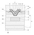
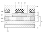
- FIG. 5 to 7 are cross-sectional views showing the semiconductor chip 1 according to the embodiment.
- FIG. 5 is a sectional view taken along line AA in FIGS. 3 and 4.
- FIG. 6 is a sectional view taken along line BB in FIGS. 3 and 4.
- FIG. 7 is a sectional view taken along line CC in FIGS. 3 and 4.
- FIG. 5 is a sectional view taken along line AA in FIGS. 3 and 4.
- FIG. 6 is a sectional view taken along line BB in FIGS. 3 and 4.
- FIG. 7 is a sectional view taken along line CC in FIGS. 3 and 4.
- the semiconductor chip 1 mainly includes a silicon carbide substrate 10, a gate insulating film 21, a gate wiring 22, an interlayer insulating film 23, a source electrode 30, It has a drain electrode 40.
- Silicon carbide substrate 10 is an example of a semiconductor substrate. When using silicon carbide substrate 10, it is easy to obtain excellent breakdown voltage. Silicon carbide substrate 10 includes a silicon carbide single crystal substrate 11 and a silicon carbide epitaxial layer 12 on silicon carbide single crystal substrate 11 . Silicon carbide substrate 10 has a first main surface 10A and a second main surface 10B opposite to the first main surface 10A. Silicon carbide epitaxial layer 12 constitutes first principal surface 10A, and silicon carbide single crystal substrate 11 constitutes second principal surface 10B. Silicon carbide single crystal substrate 11 and silicon carbide epitaxial layer 12 are made of, for example, hexagonal silicon carbide of polytype 4H. Silicon carbide single crystal substrate 11 contains an n-type impurity such as nitrogen (N), and has n-type conductivity type. A plurality of transistor cells 100 are formed on a silicon carbide substrate 10.
- N nitrogen
- Silicon carbide epitaxial layer 12 mainly includes a drift region 13 , a body region 14 , a source region 15 , a contact region 16 , an electric field relaxation region 17 , and a connection region 18 .
- the drift region 13 contains an n-type impurity such as nitrogen or phosphorus (P), and has an n-type conductivity type.
- the drift region 13 has a first region 13A, a second region 13B, and a third region 13C.
- Body region 14 is provided above the drift region 13.
- Body region 14 contains, for example, a p-type impurity such as aluminum (Al), and has p-type conductivity type.
- Source region 15 is provided on the body region 14.
- Source region 15 contains an n-type impurity such as nitrogen or phosphorus, and has n-type conductivity.
- Source region 15 is separated from drift region 13 by body region 14 .
- Source region 15 constitutes first main surface 10A.
- Contact region 16 contains, for example, a p-type impurity such as aluminum, and has p-type conductivity type. Contact region 16 penetrates source region 15 and contacts body region 14 . Contact region 16 constitutes first main surface 10A.
- the effective concentration of p-type impurities in the contact region 16 is, for example, 1 ⁇ 10 18 cm ⁇ 3 or more and 2 ⁇ 10 20 cm ⁇ 3 or less.
- a gate trench 5 defined by a side surface 3 and a bottom surface 4 is provided on the first main surface 10A.
- Side surface 3 penetrates source region 15 and body region 14 to reach drift region 13 .
- the side surface 3 may be, for example, a surface inclined from the second main surface 10B, or a surface perpendicular to the second main surface 10B.
- the bottom surface 4 is continuous with the side surface 3.
- the bottom surface 4 is in the drift region 13.
- the bottom surface 4 is, for example, a plane parallel to the second main surface 10B.
- the gate trench 5 is provided, for example, in an island shape along the X-axis direction. When viewed in plan from a direction perpendicular to the first main surface 10A, the plurality of gate trenches 5 are provided at regular intervals in the Y-axis direction.
- the electric field relaxation region 17 contains a p-type impurity such as aluminum, and has a p-type conductivity type.
- the electric field relaxation region 17 extends along the X-axis direction.
- Electric field relaxation region 17 is located between body region 14 and second main surface 10B. When viewed in plan from a direction perpendicular to the first main surface 10A, the electric field relaxation region 17 includes a portion that overlaps with the gate trench 5.
- the electric field relaxation region 17 relieves electric field concentration on the gate insulating film 21 in contact with the bottom surface 4 when a high voltage is applied.
- the upper end surface of the electric field relaxation region 17 is separated from the bottom surface 4 in the direction perpendicular to the second main surface 10B.
- the upper end surface of the electric field relaxation region 17 may include the bottom surface 4 of the gate trench 5. A portion of the upper end surface of electric field relaxation region 17 faces a portion of the lower end surface of body region 14 .
- Electric field relaxation region 17 is electrically connected to source electrode 30 . In this case, the electric field relaxation region 17 becomes the source potential, and the parasitic capacitance between the gate wiring 22 and the drain electrode 40 can be reduced. Therefore, switching speed is improved.
- the effective concentration of p-type impurities in the electric field relaxation region 17 is, for example, 5 ⁇ 10 17 cm ⁇ 3 or more and 5 ⁇ 10 18 cm ⁇ 3 or less.
- the electric field relaxation region 17 is an example of a first semiconductor region.
- connection region 18 contains, for example, a p-type impurity such as aluminum, and has a p-type conductivity type.
- the connection region 18 penetrates the first region 13A and reaches the electric field relaxation region 17.
- Connection region 18 electrically connects body region 14 and electric field relaxation region 17 .
- a current flows from the source electrode 30 to the electric field relaxation region 17 through the contact region 16, the body region 14, and the connection region 18 in this order.
- Connection region 18 contacts body region 14 .
- Connection region 18 may contact contact region 16 .
- Connection region 18 may contact each of body region 14 and contact region 16 .
- Connection region 18 is between contact region 16 and electric field relaxation region 17 .
- Connection region 18 is closer to second main surface 10B than contact region 16 is.
- connection region 18 is located closer to the first main surface 10A than the electric field relaxation region 17 is.
- a plurality of connection regions 18 are arranged at regular intervals along the X-axis direction, for example.
- the effective concentration of p-type impurities in connection region 18 may be approximately the same as the effective concentration of p-type impurities in electric field relaxation region 17 .
- the effective concentration of p-type impurities in the connection region 18 is, for example, 5 ⁇ 10 17 cm ⁇ 3 or more and 5 ⁇ 10 18 cm ⁇ 3 or less.
- Connection region 18 is an example of a second semiconductor region.
- connection regions 18 are arranged at different positions in the X-axis direction with respect to the connection regions 18 of adjacent transistor cells 100. In this case, as shown by the arrows in FIG. 3, currents in opposite directions tend to flow through adjacent electric field relaxation regions 17.
- connection region 18 may be, for example, between two connection regions 18 of adjacent transistor cells 100 that are adjacent in the X-axis direction. In this case, it is easy to flow currents in opposite directions to adjacent electric field relaxation regions 17 .
- the first region 13A of the drift region 13 is located between the body region 14 and the electric field relaxation region 17.
- the first region 13A is in contact with the body region 14 and the electric field relaxation region 17.
- the first region 13A is closer to the first main surface 10A than the electric field relaxation region 17 is.
- the second region 13B is closer to the second main surface 10B than the first region 13A.
- the second region 13B is continuous with the first region 13A.
- the second region 13B contacts the electric field relaxation region 17 in a direction parallel to the second main surface 10B.
- the second region 13B and the electric field relaxation region 17 may be located on the same plane parallel to the second main surface 10B.
- the effective concentration of n-type impurities in the second region 13B may be higher than the effective concentration of n-type impurities in the first region 13A.
- the third region 13C is closer to the second main surface 10B than the second region 13B.
- the third region 13C is continuous with the second region 13B.
- the third region 13C contacts the electric field relaxation region 17.
- the third region 13C is closer to the second main surface 10B than the electric field relaxation region 17 is.
- Third region 13C may be between second region 13B and silicon carbide single crystal substrate 11.
- Third region 13C may be continuous with silicon carbide single crystal substrate 11.
- the effective concentration of n-type impurities in the third region 13C may be the same as the effective concentration of n-type impurities in the second region 13B.
- the gate insulating film 21 is, for example, an oxide film.
- the gate insulating film 21 is made of a material containing silicon dioxide, for example.
- the gate insulating film 21 is in contact with the side surfaces 3 and the bottom surface 4.
- the gate insulating film 21 contacts the first region 13A at the bottom surface 4.
- the gate insulating film 21 contacts the source region 15, the body region 14, and the first region 13A at the side surface 3.
- Gate insulating film 21 may be in contact with source region 15 on first main surface 10A.
- the gate wiring 22 is provided on the gate insulating film 21.
- the gate wiring 22 is made of, for example, polysilicon containing conductive impurities.
- Gate wiring 22 is provided inside gate trench 5 . A portion of the gate wiring 22 may be provided on the first main surface 10A.
- the interlayer insulating film 23 covers the gate wiring 22.
- the interlayer insulating film 23 is in contact with the gate wiring 22 and the gate insulating film 21 .
- the interlayer insulating film 23 is, for example, an oxide film.
- the interlayer insulating film 23 is made of a material containing silicon dioxide, for example. Interlayer insulating film 23 electrically insulates gate wiring 22 and source electrode 30 from each other. A part of the interlayer insulating film 23 may be provided inside the gate trench 5.
- a contact hole 24 is formed in the interlayer insulating film 23 and the gate insulating film 21.
- Contact holes 24 are provided at regular intervals in the Y-axis direction. The contact holes 24 are provided so that the gate trench 5 is located between the contact holes 24 adjacent in the Y-axis direction when viewed in plan from a direction perpendicular to the first main surface 10A.
- Contact hole 24 extends along the X-axis direction. Source region 15 and contact region 16 are exposed from interlayer insulating film 23 and gate insulating film 21 through contact hole 24 . The contact regions 16 do not need to be provided over the entire area in the X-axis direction, and may be provided periodically.
- a barrier metal film may be formed to cover the upper surface and side surfaces of the interlayer insulating film 23 and the side surfaces of the gate insulating film 21.
- the source electrode 30 is in contact with the first main surface 10A.
- the source electrode 30 has a contact electrode 31 and a source wiring 32.
- the contact electrode 31 contacts the source region 15 and the contact region 16 on the first main surface 10A.
- the contact electrode 31 is made of a material containing, for example, nickel silicide (NiSi).
- Contact electrode 31 may be made of a material containing titanium, aluminum, and silicon. Contact electrode 31 makes an ohmic contact with contact region 16 .
- the source wiring 32 covers the upper surface and side surfaces of the interlayer insulating film 23 and the upper surface of the contact electrode 31.
- the source wiring 32 is in contact with the contact electrode 31.
- the source wiring 32 is made of a material containing aluminum, for example.
- the drain electrode 40 is in contact with the second main surface 10B. Drain electrode 40 contacts silicon carbide single crystal substrate 11 at second main surface 10B. Drain electrode 40 is electrically connected to drift region 13 .
- the drain electrode 40 is made of a material containing, for example, nickel silicide. Drain electrode 40 may be made of a material containing titanium, aluminum, and silicon. Drain electrode 40 makes an ohmic contact with silicon carbide single crystal substrate 11 .
Landscapes
- Electrodes Of Semiconductors (AREA)
Priority Applications (3)
| Application Number | Priority Date | Filing Date | Title |
|---|---|---|---|
| CN202280094397.8A CN118872069A (zh) | 2022-05-19 | 2022-12-19 | 半导体芯片 |
| JP2024521548A JPWO2023223588A1 (https=) | 2022-05-19 | 2022-12-19 | |
| DE112022007247.4T DE112022007247T5 (de) | 2022-05-19 | 2022-12-19 | Halbleiter-Chip |
Applications Claiming Priority (2)
| Application Number | Priority Date | Filing Date | Title |
|---|---|---|---|
| JP2022082047 | 2022-05-19 | ||
| JP2022-082047 | 2022-05-19 |
Publications (1)
| Publication Number | Publication Date |
|---|---|
| WO2023223588A1 true WO2023223588A1 (ja) | 2023-11-23 |
Family
ID=88835148
Family Applications (1)
| Application Number | Title | Priority Date | Filing Date |
|---|---|---|---|
| PCT/JP2022/046591 Ceased WO2023223588A1 (ja) | 2022-05-19 | 2022-12-19 | 半導体チップ |
Country Status (4)
| Country | Link |
|---|---|
| JP (1) | JPWO2023223588A1 (https=) |
| CN (1) | CN118872069A (https=) |
| DE (1) | DE112022007247T5 (https=) |
| WO (1) | WO2023223588A1 (https=) |
Citations (6)
| Publication number | Priority date | Publication date | Assignee | Title |
|---|---|---|---|---|
| JP2017139441A (ja) * | 2016-02-01 | 2017-08-10 | 富士電機株式会社 | 炭化珪素半導体装置および炭化珪素半導体装置の製造方法 |
| WO2017175460A1 (ja) * | 2016-04-07 | 2017-10-12 | 三菱電機株式会社 | 半導体装置および電力変換装置 |
| WO2019155783A1 (ja) * | 2018-02-06 | 2019-08-15 | 住友電気工業株式会社 | 炭化珪素半導体装置 |
| US20190259870A1 (en) * | 2018-02-21 | 2019-08-22 | Infineon Technologies Ag | Silicon Carbide Semiconductor Device Having a Gate Electrode Formed in a Trench Structure |
| JP2020119939A (ja) * | 2019-01-21 | 2020-08-06 | 株式会社デンソー | 半導体装置 |
| JP2021114496A (ja) * | 2020-01-16 | 2021-08-05 | 信一郎 高谷 | 縦型窒化物半導体トランジスタ装置 |
Family Cites Families (2)
| Publication number | Priority date | Publication date | Assignee | Title |
|---|---|---|---|---|
| JP5630114B2 (ja) | 2010-07-16 | 2014-11-26 | トヨタ自動車株式会社 | 炭化珪素半導体装置 |
| JP2022082047A (ja) | 2020-11-20 | 2022-06-01 | 住友ゴム工業株式会社 | 搬送台車、及び搬送方法 |
-
2022
- 2022-12-19 WO PCT/JP2022/046591 patent/WO2023223588A1/ja not_active Ceased
- 2022-12-19 JP JP2024521548A patent/JPWO2023223588A1/ja active Pending
- 2022-12-19 DE DE112022007247.4T patent/DE112022007247T5/de active Pending
- 2022-12-19 CN CN202280094397.8A patent/CN118872069A/zh active Pending
Patent Citations (6)
| Publication number | Priority date | Publication date | Assignee | Title |
|---|---|---|---|---|
| JP2017139441A (ja) * | 2016-02-01 | 2017-08-10 | 富士電機株式会社 | 炭化珪素半導体装置および炭化珪素半導体装置の製造方法 |
| WO2017175460A1 (ja) * | 2016-04-07 | 2017-10-12 | 三菱電機株式会社 | 半導体装置および電力変換装置 |
| WO2019155783A1 (ja) * | 2018-02-06 | 2019-08-15 | 住友電気工業株式会社 | 炭化珪素半導体装置 |
| US20190259870A1 (en) * | 2018-02-21 | 2019-08-22 | Infineon Technologies Ag | Silicon Carbide Semiconductor Device Having a Gate Electrode Formed in a Trench Structure |
| JP2020119939A (ja) * | 2019-01-21 | 2020-08-06 | 株式会社デンソー | 半導体装置 |
| JP2021114496A (ja) * | 2020-01-16 | 2021-08-05 | 信一郎 高谷 | 縦型窒化物半導体トランジスタ装置 |
Also Published As
| Publication number | Publication date |
|---|---|
| DE112022007247T5 (de) | 2025-03-06 |
| CN118872069A (zh) | 2024-10-29 |
| JPWO2023223588A1 (https=) | 2023-11-23 |
Similar Documents
| Publication | Publication Date | Title |
|---|---|---|
| US12154900B2 (en) | Semiconductor device and semiconductor package | |
| US6825565B2 (en) | Semiconductor device | |
| JP2023179690A (ja) | SiC半導体装置 | |
| US11664448B2 (en) | Semiconductor device | |
| JP7674656B2 (ja) | 炭化ケイ素半導体装置 | |
| US8178910B2 (en) | Semiconductor device | |
| CN116598354A (zh) | 一种基于多边形元胞的沟槽型功率mosfet器件及工艺流程 | |
| JP7705037B2 (ja) | 炭化ケイ素半導体装置およびその製造方法 | |
| US7205628B2 (en) | Semiconductor device | |
| US20240162297A1 (en) | Silicon carbide semiconductor device | |
| WO2023223588A1 (ja) | 半導体チップ | |
| WO2023189054A1 (ja) | 半導体装置 | |
| WO2023223590A1 (ja) | 半導体チップ | |
| WO2023223589A1 (ja) | 半導体チップ | |
| CN116799061A (zh) | 半导体装置 | |
| US20260032990A1 (en) | Semiconductor device | |
| US20250098262A1 (en) | Semiconductor device | |
| US20260090075A1 (en) | Semiconductor device | |
| US20260020325A1 (en) | Semiconductor device | |
| US20240055474A1 (en) | Semiconductor device | |
| WO2025121295A1 (ja) | 炭化珪素半導体装置 | |
| WO2025126575A1 (ja) | 半導体装置 | |
| WO2025127078A1 (ja) | 炭化珪素半導体装置 | |
| JP2025101790A (ja) | 炭化珪素半導体装置 | |
| JP2024124050A (ja) | 炭化珪素半導体装置 |
Legal Events
| Date | Code | Title | Description |
|---|---|---|---|
| 121 | Ep: the epo has been informed by wipo that ep was designated in this application |
Ref document number: 22942789 Country of ref document: EP Kind code of ref document: A1 |
|
| WWE | Wipo information: entry into national phase |
Ref document number: 18843507 Country of ref document: US |
|
| ENP | Entry into the national phase |
Ref document number: 2024521548 Country of ref document: JP Kind code of ref document: A |
|
| WWE | Wipo information: entry into national phase |
Ref document number: 202280094397.8 Country of ref document: CN |
|
| WWE | Wipo information: entry into national phase |
Ref document number: 112022007247 Country of ref document: DE |
|
| WWP | Wipo information: published in national office |
Ref document number: 112022007247 Country of ref document: DE |
|
| 122 | Ep: pct application non-entry in european phase |
Ref document number: 22942789 Country of ref document: EP Kind code of ref document: A1 |