WO2023219046A1 - 窒化物半導体装置 - Google Patents
窒化物半導体装置 Download PDFInfo
- Publication number
- WO2023219046A1 WO2023219046A1 PCT/JP2023/017197 JP2023017197W WO2023219046A1 WO 2023219046 A1 WO2023219046 A1 WO 2023219046A1 JP 2023017197 W JP2023017197 W JP 2023017197W WO 2023219046 A1 WO2023219046 A1 WO 2023219046A1
- Authority
- WO
- WIPO (PCT)
- Prior art keywords
- layer
- nitride semiconductor
- dummy
- gate
- semiconductor device
- Prior art date
- Legal status (The legal status is an assumption and is not a legal conclusion. Google has not performed a legal analysis and makes no representation as to the accuracy of the status listed.)
- Ceased
Links
Images








Classifications
-
- H—ELECTRICITY
- H10—SEMICONDUCTOR DEVICES; ELECTRIC SOLID-STATE DEVICES NOT OTHERWISE PROVIDED FOR
- H10D—INORGANIC ELECTRIC SEMICONDUCTOR DEVICES
- H10D30/00—Field-effect transistors [FET]
- H10D30/01—Manufacture or treatment
- H10D30/051—Manufacture or treatment of FETs having PN junction gates
-
- H—ELECTRICITY
- H10—SEMICONDUCTOR DEVICES; ELECTRIC SOLID-STATE DEVICES NOT OTHERWISE PROVIDED FOR
- H10D—INORGANIC ELECTRIC SEMICONDUCTOR DEVICES
- H10D30/00—Field-effect transistors [FET]
- H10D30/01—Manufacture or treatment
- H10D30/061—Manufacture or treatment of FETs having Schottky gates
-
- H—ELECTRICITY
- H10—SEMICONDUCTOR DEVICES; ELECTRIC SOLID-STATE DEVICES NOT OTHERWISE PROVIDED FOR
- H10D—INORGANIC ELECTRIC SEMICONDUCTOR DEVICES
- H10D30/00—Field-effect transistors [FET]
- H10D30/40—FETs having zero-dimensional [0D], one-dimensional [1D] or two-dimensional [2D] charge carrier gas channels
- H10D30/47—FETs having zero-dimensional [0D], one-dimensional [1D] or two-dimensional [2D] charge carrier gas channels having two-dimensional [2D] charge carrier gas channels, e.g. nanoribbon FETs or high electron mobility transistors [HEMT]
-
- H—ELECTRICITY
- H10—SEMICONDUCTOR DEVICES; ELECTRIC SOLID-STATE DEVICES NOT OTHERWISE PROVIDED FOR
- H10D—INORGANIC ELECTRIC SEMICONDUCTOR DEVICES
- H10D30/00—Field-effect transistors [FET]
- H10D30/80—FETs having rectifying junction gate electrodes
- H10D30/83—FETs having PN junction gate electrodes
-
- H—ELECTRICITY
- H10—SEMICONDUCTOR DEVICES; ELECTRIC SOLID-STATE DEVICES NOT OTHERWISE PROVIDED FOR
- H10D—INORGANIC ELECTRIC SEMICONDUCTOR DEVICES
- H10D30/00—Field-effect transistors [FET]
- H10D30/80—FETs having rectifying junction gate electrodes
- H10D30/87—FETs having Schottky gate electrodes, e.g. metal-semiconductor FETs [MESFET]
-
- H—ELECTRICITY
- H10—SEMICONDUCTOR DEVICES; ELECTRIC SOLID-STATE DEVICES NOT OTHERWISE PROVIDED FOR
- H10D—INORGANIC ELECTRIC SEMICONDUCTOR DEVICES
- H10D62/00—Semiconductor bodies, or regions thereof, of devices having potential barriers
- H10D62/80—Semiconductor bodies, or regions thereof, of devices having potential barriers characterised by the materials
- H10D62/83—Semiconductor bodies, or regions thereof, of devices having potential barriers characterised by the materials being Group IV materials, e.g. B-doped Si or undoped Ge
-
- H—ELECTRICITY
- H10—SEMICONDUCTOR DEVICES; ELECTRIC SOLID-STATE DEVICES NOT OTHERWISE PROVIDED FOR
- H10D—INORGANIC ELECTRIC SEMICONDUCTOR DEVICES
- H10D64/00—Electrodes of devices having potential barriers
- H10D64/01—Manufacture or treatment
- H10D64/011—Manufacture or treatment of electrodes ohmically coupled to a semiconductor
-
- H—ELECTRICITY
- H10—SEMICONDUCTOR DEVICES; ELECTRIC SOLID-STATE DEVICES NOT OTHERWISE PROVIDED FOR
- H10D—INORGANIC ELECTRIC SEMICONDUCTOR DEVICES
- H10D64/00—Electrodes of devices having potential barriers
- H10D64/20—Electrodes characterised by their shapes, relative sizes or dispositions
-
- H—ELECTRICITY
- H10—SEMICONDUCTOR DEVICES; ELECTRIC SOLID-STATE DEVICES NOT OTHERWISE PROVIDED FOR
- H10D—INORGANIC ELECTRIC SEMICONDUCTOR DEVICES
- H10D64/00—Electrodes of devices having potential barriers
- H10D64/20—Electrodes characterised by their shapes, relative sizes or dispositions
- H10D64/23—Electrodes carrying the current to be rectified, amplified, oscillated or switched, e.g. sources, drains, anodes or cathodes
Definitions
- the present disclosure relates to a nitride semiconductor device.
- HEMTs high electron mobility transistors
- nitride semiconductors nitride semiconductors
- a normally-off operation is required from the viewpoint of fail-safety, in which the current path (channel) between the source and drain is cut off at zero bias.
- a second nitride semiconductor layer (electron supply layer) having a different band gap (Al composition) is formed on the first nitride semiconductor layer (electron transit layer).
- a heterojunction is formed.
- a two-dimensional electron gas is formed in the first nitride semiconductor layer near the interface between the first nitride semiconductor layer and the second nitride semiconductor layer.
- the energy levels of the first nitride semiconductor layer and the second nitride semiconductor layer are raised by ionized acceptors contained in a gallium nitride (GaN) layer doped with acceptor-type impurities.
- GaN gallium nitride
- the energy level of the conduction band at the heterojunction interface becomes higher than the Fermi level.
- the channel caused by the two-dimensional electron gas is blocked directly under the gate electrode, thereby realizing a normally-off type HEMT.
- the shape of the GaN layer doped with acceptor-type impurities greatly affects the operating characteristics of the HEMT (for example, on-resistance, gate threshold voltage, maximum rating of gate-source voltage, etc.). Therefore, if the shape of the p-type GaN layer is non-uniform within the chip, gate reliability may decrease.
- a nitride semiconductor device includes a nitride semiconductor layer and a gate layer formed on the nitride semiconductor layer, which extends in a first direction in a plan view and is orthogonal to the first direction.
- a gate layer including a plurality of main gate portions arranged in a second direction; a gate electrode formed on the gate layer; a passivation layer covering the gate layer, the gate electrode, the first dummy part, and the second dummy part, the passivation layer having a plurality of source openings and a plurality of drain openings; a source electrode in contact with the nitride semiconductor layer through the plurality of source openings, and a drain electrode in contact with the nitride semiconductor layer through the plurality of drain openings.
- the gate layer, the first dummy part, and the second dummy part are made of a nitride semiconductor containing acceptor type impurities.
- the gate layer, the plurality of source openings, and the plurality of drain openings are arranged between the first dummy part and the second dummy part, which are spaced apart in the second direction in plan view.
- the uniformity of the shape of the main gate portion can be improved.
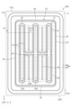
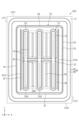
- FIG. 1 is a schematic plan view of an exemplary nitride semiconductor device according to one embodiment.
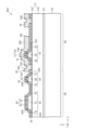
- FIG. 2 is a schematic cross-sectional view of the nitride semiconductor device taken along line F2-F2 in FIG.
- FIG. 3 is a schematic cross-sectional view showing an exemplary manufacturing process of an active region nitride semiconductor device.
- FIG. 4 is a schematic cross-sectional view showing a manufacturing process subsequent to the process shown in FIG. 3.
- FIG. 5 is a schematic cross-sectional view showing a manufacturing process following the process shown in FIG. 4.
- FIG. 6 is a schematic cross-sectional view showing a manufacturing process subsequent to the process shown in FIG.
- FIG. 7 is a schematic cross-sectional view showing a manufacturing process following the process shown in FIG. 6.
- FIG. 8 is a schematic cross-sectional view showing a manufacturing process subsequent to the process shown in FIG. 7.
- FIG. 9 is a schematic cross-sectional view showing a manufacturing process following the process shown in FIG. 8.
- FIG. 10 is a schematic cross-sectional view showing a manufacturing process subsequent to the process shown in FIG.
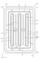
- FIG. 11 is a schematic plan view of an exemplary nitride semiconductor device according to the first modification.
- FIG. 12 is a schematic plan view of an exemplary nitride semiconductor device according to a second modification example.
- FIG. 13 is a schematic plan view of an exemplary nitride semiconductor device according to a third modification.
- FIG. 14 is a schematic cross-sectional view of the nitride semiconductor device taken along line F14-F14 in FIG. 13.
- FIG. 15 is a schematic plan view of an exemplary nitride semiconductor device according to a fourth modification.
- FIG. 16 is a schematic plan view of an exemplary nitride semiconductor device according to a fifth modification.
- FIG. 17 is a schematic cross-sectional view of the nitride semiconductor device taken along line F17-F17 in FIG. 16.
- FIG. 18 is a schematic plan view of an exemplary nitride semiconductor device according to a sixth modification.
- FIG. 19 is a schematic plan view of an exemplary nitride semiconductor device according to a seventh modification.
- FIG. 20 is a schematic cross-sectional view of an exemplary nitride semiconductor device according to an eighth modification.
- FIG. 21 is a schematic cross-sectional view of an exemplary nitride semiconductor device according to a ninth modification.
- FIG. 1 is a schematic plan view of an exemplary nitride semiconductor device 10 according to one embodiment.
- Nitride semiconductor device 10 includes a nitride semiconductor layer 12, a gate layer 14 formed on nitride semiconductor layer 12, and a gate electrode 16 formed on gate layer 14.
- the Z-axis direction of the mutually perpendicular XYZ axes shown in FIG. 1 is a direction perpendicular to the surface of the nitride semiconductor layer 12 on which a device is formed.
- the term "planar view” used in this specification refers to viewing the nitride semiconductor device 10 from above along the Z-axis direction, unless explicitly stated otherwise.
- the upper surface of the nitride semiconductor layer 12 can include two sides 12X1 and 12X2 extending along the X-axis direction and two sides 12Y1 and 12Y2 extending along the Y-axis direction.
- the area defined by the four sides 12X1, 12X2, 12Y1, and 12Y2 of the nitride semiconductor layer 12 may correspond to one chip (die). Further details of the nitride semiconductor layer 12 will be described later with reference to FIG.
- the gate layer 14 is made of a nitride semiconductor containing acceptor type impurities.
- the gate layer 14 may be a gallium nitride layer (p-type GaN layer) doped with acceptor type impurities.
- the acceptor type impurity can include at least one of zinc (Zn), magnesium (Mg), and carbon (C).
- the maximum concentration of acceptor type impurities in the gate layer 14 may be, for example, 7 ⁇ 10 18 cm ⁇ 3 or more and 1 ⁇ 10 20 cm ⁇ 3 or less.
- the gate layer 14 includes a plurality of main gate portions 18 that extend in the Y-axis direction (first direction) and are arranged in the X-axis direction (second direction) in plan view. Note that in this specification, the Y-axis direction is also referred to as a first direction, and the X-axis direction is also referred to as a second direction. In the example of FIG. 1, the gate layer 14 includes four main gate parts 18. The number of main gate sections 18 can be arbitrarily determined depending on the desired layout of the nitride semiconductor device 10 or the area (chip area) of the nitride semiconductor layer 12.
- the gate layer 14 may further include a plurality of gate connection parts 20 that interconnect the plurality of main gate parts 18.
- three gate connecting parts 20 connect two main gate parts 18.
- the number of gate connecting portions 20 can be arbitrarily determined depending on the desired layout of nitride semiconductor device 10 or the area (chip area) of nitride semiconductor layer 12.
- the gate connecting part 20 can be configured to connect two main gate parts 18 spaced apart in the X-axis direction.
- the gate electrode 16 may be composed of one or more metal layers.
- gate electrode 16 may be comprised of a titanium nitride (TiN) layer.
- the gate electrode 16 may include a first metal layer made of Ti and a second metal layer made of TiN provided on the first metal layer.
- the gate electrode 16 can form a Schottky junction with the gate layer 14.
- the gate electrode 16 may be formed in a region smaller than the gate layer 14 in plan view.
- the nitride semiconductor device 10 may further include a dummy pattern 22 formed on the nitride semiconductor layer 12.
- the dummy pattern 22 is formed in a closed ring shape so as to surround the gate layer 14 in plan view.
- the dummy pattern 22 may extend generally along the four sides 12X1, 12X2, 12Y1, and 12Y2 of the nitride semiconductor layer 12 in plan view.
- the dummy pattern 22 is formed on the nitride semiconductor layer 12 and includes a first dummy part 24 and a second dummy part 26 that extend in the Y-axis direction in plan view.
- the first dummy section 24 and the second dummy section 26 are made of a nitride semiconductor containing acceptor type impurities.
- the dummy pattern 22 may further include a third dummy part 28 and a fourth dummy part 30 that are formed on the nitride semiconductor layer 12 and extend in the X-axis direction in plan view.
- the third dummy section 28 and the fourth dummy section 30 are made of a nitride semiconductor containing acceptor type impurities.
- the first dummy part 24, the second dummy part 26, the third dummy part 28, and the fourth dummy part 30 constitute at least a part of the ring-shaped dummy pattern 22 in plan view. There is.
- the nitride semiconductor device 10 may further include a dummy electrode 32 formed on the dummy pattern 22.
- the dummy electrode 32 may be made of the same metal layer as the gate electrode 16.
- the dummy electrode 32 may be formed in an area smaller than the dummy pattern 22 in plan view.
- the dummy electrode 32 may be electrically floating.
- the nitride semiconductor device 10 further includes a passivation layer 34 (see FIG. 2) having a plurality of source openings 34A and a plurality of drain openings 34B.
- the passivation layer 34 is shown to be transparent so that the layers below the passivation layer 34 are visible, but the plurality of source openings 34A and the plurality of drain openings 34B are depicted in dashed lines.
- the passivation layer 34 covers the gate layer 14, the gate electrode 16, the dummy pattern 22 (the first dummy part 24, the second dummy part 26, the third dummy part 28, and the fourth dummy part 30), and the dummy electrode 32. good.
- source openings 34A and four drain openings 34B are formed in the passivation layer 34.
- Two source openings 34A spaced apart from each other are lined up in the Y-axis direction.
- two drain openings 34B spaced apart from each other are lined up in a line in the Y-axis direction.
- Source openings 34A and drain openings 34B are arranged alternately in the X-axis direction.
- the number of source openings 34A and the number of drain openings 34B can be arbitrarily determined depending on the desired layout of nitride semiconductor device 10 or the area (chip area) of nitride semiconductor layer 12.
- the number of source openings 34A and drain openings 34B can be determined depending on, for example, the number of main gate sections 18.
- Each main gate section 18 is arranged between one of the plurality of source openings 34A and one of the plurality of drain openings 34B.
- Each gate connection part 20 is spaced apart from at least one of the plurality of drain openings 34B in the Y-axis direction. Some of the plurality of gate coupling parts 20 are arranged between two drain openings 34B aligned in a row in the Y-axis direction.
- the gate layer 14, the plurality of source openings 34A, and the plurality of drain openings 34B are arranged between the first dummy part 24 and the second dummy part 26, which are separated in the X-axis direction in plan view.
- the gate layer 14, the plurality of source openings 34A, and the plurality of drain openings 34B are arranged between the third dummy part 28 and the fourth dummy part 30, which are separated in the Y-axis direction in plan view. .
- the nitride semiconductor device 10 includes a source electrode 36 in contact with the nitride semiconductor layer 12 through a plurality of source openings 34A, and a drain electrode 38 in contact with the nitride semiconductor layer 12 through a plurality of drain openings 34B. further including.
- the source electrode 36 is drawn with a chain double-dashed line, but is shown to be transparent so that the layer below the source electrode 36 can be seen.
- the source electrode 36 and the drain electrode 38 can be constituted by one or more metal layers (eg, a combination of a Ti layer, a TiN layer, an Al layer, an AlSiCu layer, an AlCu layer, etc.).
- the source electrode 36 and the drain electrode 38 are arranged between the first dummy part 24 and the second dummy part 26, which are separated in the X-axis direction in plan view. Similarly, the source electrode 36 and the drain electrode 38 are arranged between the third dummy part 28 and the fourth dummy part 30, which are separated in the Y-axis direction in plan view.
- Source electrode 36 can be arranged to partially cover gate layer 14 and gate electrode 16. Details of the source electrode 36 will be described later with reference to FIG. 2.
- Drain electrode 38 can be arranged to cover drain opening 34B. The drain electrode 38 is arranged so as not to overlap the gate layer 14 and the gate electrode 16 in plan view.
- the nitride semiconductor device 10 may further include a guard ring 40 formed on the nitride semiconductor layer.
- the guard ring 40 is formed to surround the dummy pattern 22 in plan view.
- Guard ring 40 may include a guard ring layer 42 formed on nitride semiconductor layer 12 and a guard ring electrode 44 formed on guard ring layer 42.
- the guard ring layer 42 may be made of a nitride semiconductor containing acceptor type impurities.
- the guard ring electrode 44 may be made of the same metal layer as the source electrode 36 and the drain electrode 38. Guard ring electrode 44 may be electrically connected to source electrode 36 .
- FIG. 2 is a schematic cross-sectional view of the nitride semiconductor device 10 taken along line F2-F2 in FIG.
- Nitride semiconductor device 10 may include a semiconductor substrate 50, a buffer layer 52 formed on semiconductor substrate 50, and the above-described nitride semiconductor layer 12.
- the nitride semiconductor layer 12 may include an electron transit layer 54 formed on the buffer layer 52 and an electron supply layer 56 formed on the electron transit layer 54.
- Semiconductor substrate 50 may be formed of silicon (Si), silicon carbide (SiC), GaN, sapphire, or other substrate material.
- semiconductor substrate 50 may be a Si substrate.
- the thickness of the semiconductor substrate 50 can be, for example, 200 ⁇ m or more and 1500 ⁇ m or less.
- the buffer layer 52 can be located between the semiconductor substrate 50 and the electron transit layer 54.
- buffer layer 52 can be comprised of any material that can facilitate epitaxial growth of electron transport layer 54.
- Buffer layer 52 may include one or more nitride semiconductor layers.
- buffer layer 52 can include at least one of an aluminum nitride (AlN) layer, an aluminum gallium nitride (AlGaN) layer, and a graded AlGaN layer with a different aluminum (Al) composition.
- the buffer layer 52 may be formed by a single AlN layer, a single AlGaN layer, a layer having an AlGaN/GaN superlattice structure, a layer having an AlN/AlGaN superlattice structure, or a layer having an AlN/GaN superlattice structure. may be configured.
- the buffer layer 52 may include a first buffer layer that is an AlN layer formed on the semiconductor substrate 50 and a second buffer layer that is an AlGaN layer formed on the AlN layer.
- the first buffer layer may be, for example, an AlN layer with a thickness of 200 nm
- the second buffer layer may be formed by laminating multiple graded AlGaN layers, for example, with a thickness of 300 nm. You can leave it there.
- impurities may be introduced into a part of the buffer layer 52 to make the buffer layer 52 semi-insulating.
- the impurity is, for example, carbon (C) or iron (Fe), and the concentration of the impurity can be, for example, 4 ⁇ 10 16 cm ⁇ 3 or more.
- the electron transit layer 54 is made of a nitride semiconductor.
- the electron transit layer 54 may be, for example, a GaN layer.
- the thickness of the electron transit layer 54 can be, for example, 0.5 ⁇ m or more and 2 ⁇ m or less.
- impurities may be introduced into a part of the electron transit layer 54 to make the region other than the surface layer of the electron transit layer 54 semi-insulating.
- the impurity may be, for example, C.
- the impurity concentration in the electron transit layer 54 can be, for example, 4 ⁇ 10 16 cm ⁇ 3 or more.
- the electron transit layer 54 can include a plurality of GaN layers having different impurity concentrations, for example, a C-doped GaN layer and a non-doped GaN layer.
- the C-doped GaN layer may be formed on the buffer layer 52.
- the C-doped GaN layer can have a thickness of 0.3 ⁇ m or more and 2 ⁇ m or less.
- the C concentration in the C-doped GaN layer can be set to 5 ⁇ 10 17 cm ⁇ 3 or more and 9 ⁇ 10 19 cm ⁇ 3 or less.
- the non-doped GaN layer is formed on the C-doped GaN layer and can have a thickness of 0.05 ⁇ m or more and 0.4 ⁇ m or less.
- the non-doped GaN layer is in contact with the electron supply layer 56.
- electron transit layer 54 may include a 0.4 ⁇ m thick C-doped GaN layer and a 0.4 ⁇ m thick undoped GaN layer.
- the C concentration in the C-doped GaN layer may be about 2 ⁇ 10 19 cm ⁇ 3 .
- the electron supply layer 56 is made of a nitride semiconductor having a larger band gap than the electron transit layer 54.
- the electron supply layer 56 may be, for example, an AlGaN layer.
- the electron supply layer 56 is composed of Al x Ga 1-x N, where x satisfies 0.1 ⁇ x ⁇ 0.4, more preferably 0.1 ⁇ x ⁇ 0.3.
- the electron supply layer 56 may have a thickness of 5 nm or more and 20 nm or less. In one example, electron supply layer 56 may have a thickness of 8 nm or more.
- the electron transport layer 54 and the electron supply layer 56 are made of nitride semiconductors having different lattice constants. Therefore, the nitride semiconductor (eg, GaN) forming the electron transit layer 54 and the nitride semiconductor (eg, AlGaN) forming the electron supply layer 56 form a lattice mismatched heterojunction. Due to the spontaneous polarization of the electron transit layer 54 and the electron supply layer 56 and the piezo polarization caused by crystal strain near the heterojunction interface, the energy level of the conduction band of the electron transit layer 54 near the heterojunction interface is lower than the Fermi level. It gets lower.
- the nitride semiconductor eg, GaN
- the nitride semiconductor eg, AlGaN
- two-dimensional electron gas (2DEG) spreads within the electron transit layer 54 at a position close to the heterojunction interface between the electron transit layer 54 and the electron supply layer 56 (for example, within a range of several nm from the interface). There is. Note that by increasing at least one of the Al composition and the thickness of the electron supply layer 56, the sheet carrier density of 2DEG generated in the electron transit layer 54 can be increased.
- gate layer 14 is formed on electron supply layer 56.
- the gate layer 14 may be a GaN layer having a smaller bandgap than the electron supply layer 56, which is, for example, an AlGaN layer.
- FIG. 2 a cross section of the main gate portion 18 of the gate layer 14 is shown.
- the main gate section 18 is located between the source opening 34A and the drain opening 34B. More specifically, the main gate portion 18 may be located between the source opening 34A and the drain opening 34B, and closer to the source opening 34A than the drain opening 34B.
- the source electrode 36 is in contact with the electron supply layer 56 via the source opening 34A.
- the drain electrode 38 is in contact with the electron supply layer 56 via the drain opening 34B.
- the main gate portion 18 includes a bottom surface 18A in contact with the nitride semiconductor layer 12 (electron supply layer 56) and an upper surface 18B on which the gate electrode 16 is formed.
- the main gate portion 18 includes a gate ridge portion 58 including the upper surface 18B, and a source side extension portion 60 and a drain side extension portion 62 having a thickness smaller than that of the gate ridge portion 58. It's okay to be there.
- the source side extension part 60 and the drain side extension part 62 extend outward from the gate ridge part 58 in plan view.
- the gate ridge portion 58 is depicted as the main gate portion 18, and the source side extension portion 60 and the drain side extension portion 62 are omitted.
- the source side extension portion 60 extends from the gate ridge portion 58 toward the source opening 34A in plan view. Note that the source opening 34A referred to here refers to the one closest to the gate ridge portion 58 among the plurality of source openings 34A. The source side extension portion 60 does not reach the source opening 34A. The source side extension portion 60 is separated from the source electrode 36 by the passivation layer 34 .
- the drain side extension portion 62 extends from the gate ridge portion 58 toward the drain opening 34B in plan view. Note that the drain opening 34B referred to here refers to the one closest to the gate ridge portion 58 among the plurality of drain openings 34B. The drain side extension portion 62 does not reach the drain opening 34B. The drain side extension portion 62 is separated from the drain electrode 38 by the passivation layer 34 .
- the gate ridge portion 58 is located between the source side extending portion 60 and the drain side extending portion 62, and is formed integrally with the source side extending portion 60 and the drain side extending portion 62. Due to the existence of the source-side extension portion 60 and the drain-side extension portion 62, the bottom surface 18A of the main gate portion 18 has a larger area than the top surface 18B. In the example shown in FIG. 2, the drain side extension part 62 extends longer toward the outside of the gate ridge part 58 in plan view than the source side extension part 60. That is, the drain side extension part 62 has a larger dimension in the X-axis direction than the source side extension part 60.
- the source side extension part 60 and the drain side extension part 62 may have the same dimensions in the X-axis direction.
- the source side extension portion 60 may have a dimension of, for example, 0.2 ⁇ m or more and 0.3 ⁇ m or less in the X-axis direction.
- the drain side extension portion 62 may have a dimension of, for example, 0.2 ⁇ m or more and 0.6 ⁇ m or less in the X-axis direction.
- the gate ridge portion 58 corresponds to a relatively thick portion of the main gate portion 18.
- the gate ridge portion 58 may have a thickness of, for example, 80 nm or more and 150 nm or less.
- the thickness of the main gate portion 18, particularly the gate ridge portion 58, can be determined by considering parameters including the gate threshold voltage.
- the main gate portion 18 (gate ridge portion 58) may have a thickness greater than 110 nm.
- Each of the source side extension part 60 and the drain side extension part 62 has a thickness smaller than the thickness of the gate ridge part 58.
- each of the source-side extension portion 60 and the drain-side extension portion 62 may have a thickness that is less than or equal to half the thickness of the gate ridge portion 58.
- Each of the source-side extension portion 60 and the drain-side extension portion 62 may include a flat portion having a substantially constant thickness. As shown in FIG. 2, each of the source side extension part 60 and the drain side extension part 62 may further include an inclined part having a thickness that gradually decreases as the distance from the gate ridge part 58 increases. The sloped portion is formed between the gate ridge portion 58 and the flat portion. In one example, the flat portions of the source-side extension portion 60 and the drain-side extension portion 62 may have a thickness of 5 nm or more and 25 nm or less. Note that in this specification, "substantially constant thickness” refers to a thickness within a range of manufacturing variations (for example, 20%).
- the gate electrode 16 is formed on the gate layer 14. As shown in FIG. 2, the gate electrode 16 is formed on the gate ridge portion 58 including the upper surface 18B of the main gate portion 18. As shown in FIG.
- the thickness of the gate electrode 16 may be, for example, 50 nm or more and 200 nm or less.
- the source electrode 36 may include a source contact plug portion 36A filled in the source opening 34A and a source field plate portion 36B covering the passivation layer 34.
- the source field plate section 36B may be continuous with the source contact plug section 36A. In this case, the source field plate section 36B is formed integrally with the source contact plug section 36A.
- the source field plate portion 36B includes an end portion 36C located between the drain opening 34B and the main gate portion 18 in plan view. The source field plate portion 36B extends along the surface of the passivation layer 34 from the source contact plug portion 36A to the end portion 36C toward the drain electrode 38, but is spaced apart from the drain electrode 38.
- Source field plate portion 36B extends along the non-flat surface of passivation layer 34, and therefore has a similarly non-flat surface.
- the source field plate portion 36B plays a role of alleviating electric field concentration near the end of the gate electrode 16 when a drain voltage is applied to the drain electrode 38 in a zero bias state where no gate voltage is applied to the gate electrode 16. is fulfilled.
- At least a portion of the source electrode 36 is filled in the source opening 34A, so it can make ohmic contact with the 2DEG directly below the electron supply layer 56 via the source opening 34A.
- the drain electrode 38 is filled in the drain opening 34B, it can make ohmic contact with the 2DEG directly below the electron supply layer 56 via the drain opening 34B.
- the nitride semiconductor device 10 may include an active region 64 that contributes to transistor operation and an inactive region 66 that does not contribute to transistor operation.
- an active region 64 that contributes to transistor operation
- an inactive region 66 that does not contribute to transistor operation.
- a region extending in the X-axis direction from the source opening 34A (source contact plug portion 36A) to the drain opening 34B (drain electrode 38) generally corresponds to the active region 64.
- the main gate section 18 is made of a nitride semiconductor (for example, p-type GaN) containing acceptor type impurities, the active region 64 including the main gate section 18 is capable of normally-off operation. It can function as a HEMT.
- the nitride semiconductor device 10 includes a plurality of source openings 34A and a plurality of drain openings 34B arranged alternately in the X-axis direction, and each main gate section 18 has a plurality of is disposed between one of the source openings 34A and one of the plurality of drain openings 34B. Therefore, the active areas 64 shown in FIG. 2 may be repeated with every other active area being reversed in the X-axis direction. In the case of the example in FIG. 1, a region extending in the X-axis direction from the source opening 34A closest to the first dummy section 24 to the source opening 34A closest to the second dummy section 26 may correspond to the active region 64. Further, the active region 64 may extend in the same range as the source opening 34A or the drain opening 34B in the Y-axis direction.
- a first dummy portion 24, which is a part of the dummy pattern 22, and a guard ring 40 are formed on the electron supply layer 56.
- the first dummy portion 24 is located between the guard ring 40 and the source opening 34A in the X-axis direction.
- the second dummy portion 26 can have the same cross-sectional structure as the first dummy portion 24 shown in FIG. 2. It should be noted that the description regarding the first dummy section 24 is equally applicable to the second dummy section 26.
- the first dummy portion 24 is made of a nitride semiconductor containing acceptor type impurities.
- the first dummy portion 24 includes a bottom surface 24A in contact with the nitride semiconductor layer 12 (electron supply layer 56), and an upper surface 24B on the opposite side of the bottom surface 24A.
- the first dummy portion 24 includes a dummy ridge portion 68 including the upper surface 24B, and an outer extending portion 70 and an inner extending portion 72 having a thickness smaller than that of the dummy ridge portion 68. It's okay to stay. Note that in the plan view shown in FIG.
- a dummy ridge portion 68 is depicted as the first dummy portion 24, and the outer extending portion 70 and the inner extending portion 72 are omitted.
- the dummy electrode 32 is formed on the upper surface 24B of the first dummy part 24.
- the first dummy part 24 and the dummy electrode 32 formed on the first dummy part 24 are covered with a passivation layer 34.
- the outer extending portion 70 extends from the dummy ridge portion 68 toward the guard ring 40 in plan view.
- the dummy pattern 22 since the dummy pattern 22 is formed in a ring shape in a plan view, the dummy pattern 22 separates the inner region surrounded by the dummy pattern 22 from the outer region of the dummy pattern 22. There is.
- the outer extending portion 70 exists in a region outside the dummy pattern 22 . In the example of FIG. 2, the outer extension 70 does not reach the guard ring 40. Outer extension 70 is spaced from guard ring 40 by passivation layer 34 .
- the inner extending portion 72 extends from the dummy ridge portion 68 toward the gate layer 14 (main gate portion 18) in plan view.
- the inner extending portion 72 exists in an inner region surrounded by the dummy pattern 22 .
- the inner extension portion 72 does not reach the source opening 34A.
- Inner extension 72 is spaced from source electrode 36 by passivation layer 34 .
- the dummy ridge portion 68 of the first dummy portion 24 is located between the outer extending portion 70 and the inner extending portion 72, and is formed integrally with the outer extending portion 70 and the inner extending portion 72. Due to the presence of the outer extending portion 70 and the inner extending portion 72, the bottom surface 24A of the first dummy portion 24 has a larger area than the top surface 24B. As shown in FIG. 2, the outer extending portion 70 and the inner extending portion 72 may have the same dimensions in the X-axis direction. The outer extending portion 70 and the inner extending portion 72 may have a dimension of, for example, 0.2 ⁇ m or more and 0.3 ⁇ m or less in the X-axis direction.
- the dummy ridge portion 68 corresponds to a relatively thick portion of the first dummy portion 24.
- the dummy ridge portion 68 may have a thickness of 80 nm or more and 150 nm or less.
- Each of the outer extension portion 70 and the inner extension portion 72 has a thickness smaller than the thickness of the dummy ridge portion 68. In one example, each of the outer extension portion 70 and the inner extension portion 72 may have a thickness that is less than or equal to half the thickness of the dummy ridge portion 68.
- Each of the outer extension portion 70 and the inner extension portion 72 may include a flat portion having a substantially constant thickness.
- Each of the outer extension portion 70 and the inner extension portion 72 may further include an inclined portion having a thickness that gradually decreases as the distance from the dummy ridge portion 68 increases, as shown in FIG. 2 .
- the sloped portion is formed between the dummy ridge portion 68 and the flat portion.
- the flat portions of the outer extending portion 70 and the inner extending portion 72 may have a thickness of 5 nm or more and 25 nm or less.
- the first dummy portion 24 is formed by the same manufacturing process as the main gate portion 18 (described later with reference to FIGS. 3 to 10). Therefore, the first dummy part 24 can have a thickness comparable to that of the main gate part 18 within the range of manufacturing variations.
- the dimension (design dimension) of the dummy ridge portion 68 in the X-axis direction may be the same as the dimension (design dimension) of the gate ridge portion 58 in the X-axis direction.
- the dimensions in the X-axis direction (design dimensions) of the outer extension part 70 and the inner extension part 72 of the first dummy part 24 are the dimensions (design dimensions) in the X-axis direction of the source side extension part 60 and the drain side extension part 62, respectively.
- the dimensions in the X-axis direction of the outer extending portion 70 and the inner extending portion 72 of the first dummy portion 24 may be the same.
- the dimensions of the outer extending portion 70 and the inner extending portion 72 in the X-axis direction may be, for example, the same as the dimension of the drain-side extending portion 62 in the X-axis direction.
- the source opening 34A located between the gate layer 14 and the first dummy part 24 may be arranged at an equal distance from both the gate layer 14 (main gate part 18) and the first dummy part 24 in plan view.
- the guard ring layer 42 is made of a nitride semiconductor containing acceptor type impurities.
- Guard ring layer 42 includes a bottom surface 42A in contact with nitride semiconductor layer 12 (electron supply layer 56), and an upper surface 24B on which guard ring electrode 44 is formed.
- the guard ring layer 42 includes a guard ring ridge portion 74 including the upper surface 42B, and an outer extending portion 76 and an inner extending portion 78 having a thickness smaller than the guard ring ridge portion 74. It's okay to be there. Note that in the plan view shown in FIG.
- a guard ring ridge portion 74 is depicted as the guard ring layer 42, and the outer extending portion 76 and the inner extending portion 78 are omitted.
- the guard ring electrode 44 is formed on the upper surface 42B of the guard ring layer 42.
- the guard ring layer 42 and the guard ring electrode 44 formed on the guard ring layer 42 are covered with a passivation layer 34.
- the outer extending portion 76 extends from the guard ring ridge portion 74 toward the outer side of the guard ring 40 in plan view. As shown in FIG. 1, the guard ring 40 is formed into a ring shape in plan view, so the guard ring 40 has an inner region surrounded by the guard ring 40 and an outer region of the guard ring 40. Separated. The outer extension 76 is present in the outer region of the guard ring 40 .
- the inner extending portion 78 extends from the guard ring ridge portion 74 toward the inner side of the guard ring 40 in plan view.
- the inner extending portion 78 exists in an inner region surrounded by the guard ring 40 . In the example of FIG. 2, the inner extending portion 78 does not reach the first dummy portion 24.
- the inner extension portion 78 is separated from the first dummy portion 24 by the passivation layer 34 .
- the guard ring ridge portion 74 of the guard ring layer 42 is located between the outer extending portion 76 and the inner extending portion 78, and is formed integrally with the outer extending portion 76 and the inner extending portion 78. Due to the presence of the outer extension portion 76 and the inner extension portion 78, the bottom surface 42A of the guard ring layer 42 has a larger area than the top surface 42B. As shown in FIG. 2, the outer extending portion 76 and the inner extending portion 78 may have the same length in the X-axis direction. The outer extending portion 76 and the inner extending portion 78 may have a length of, for example, 0.2 ⁇ m or more and 0.3 ⁇ m or less in the X-axis direction.
- the guard ring ridge portion 74 corresponds to a relatively thick portion of the guard ring layer 42, and can have a thickness of 80 nm or more and 150 nm or less.
- Each of the outer extension 76 and the inner extension 78 has a thickness that is less than the thickness of the guard ring ridge 74.
- each of the outer extensions 76 and the inner extensions 78 may have a thickness that is less than or equal to half the thickness of the guard ring ridge 74.
- Each of the outer extension portion 76 and the inner extension portion 78 may include a flat portion having a substantially constant thickness.
- Each of the outer extension portion 76 and the inner extension portion 78 may further include a sloped portion having a thickness that gradually decreases as the distance from the guard ring ridge portion 74 increases, as shown in FIG. 2 .
- the sloped portion is formed between the guard ring ridge portion 74 and the flat portion.
- the flat portions of the outer extending portion 76 and the inner extending portion 78 may have a thickness of 5 nm or more and 25 nm or less.
- the guard ring layer 42 is formed by the same manufacturing process as the main gate portion 18 (described later with reference to FIGS. 3 to 10). Therefore, the guard ring layer 42 may have a thickness comparable to that of the main gate portion 18 within the range of manufacturing variations.
- the width of the guard ring ridge portion 74 (the dimension in the X-axis direction in FIG. 2) is larger than the dimension of any of the source opening 34A, the drain opening 34B, and the gate ridge portion 58 in the X-axis direction.
- the dimensions in the X-axis direction of the outer extending portion 76 and the inner extending portion 78 of the guard ring layer 42 may be the same or different.
- the first dummy portion 24 and guard ring layer 42 described above do not directly contribute to the transistor operation of the nitride semiconductor device 10.
- a region where the dummy pattern 22 including the first dummy portion 24 and the guard ring 40 including the guard ring layer 42 are formed is included in the inactive region 66 .
- FIGS. 3 to 10 are schematic cross-sectional views showing exemplary manufacturing steps of the nitride semiconductor device 10. Note that, in order to facilitate understanding, in FIGS. 3 to 10, the same reference numerals may be given to the same components as those in FIG. 2.
- the method for manufacturing the nitride semiconductor device 10 includes forming a buffer layer 52, an electron transit layer 54, an electron supply layer 56, a gallium nitride (GaN) layer 80, on a semiconductor substrate 50, which is a Si substrate, for example. This includes sequentially forming a metal layer 82.
- the buffer layer 52, the electron transit layer 54, the electron supply layer 56, and the GaN layer 80 can be epitaxially grown using a metal organic chemical vapor deposition (MOCVD) method.
- MOCVD metal organic chemical vapor deposition
- the metal layer 82 can be formed using a sputtering method.
- the buffer layer 52 may be a multilayer buffer layer.
- the multilayer buffer layer may include an AlN layer (first buffer layer) formed on the semiconductor substrate 50 and a graded AlGaN layer (second buffer layer) formed on the AlN layer.
- the graded AlGaN layer can be formed, for example, by stacking three AlGaN layers with Al compositions of 75%, 50%, and 25% in order from the side closest to the AlN layer.
- the electron transit layer 54 formed on the buffer layer 52 may be a GaN layer.
- the electron supply layer 56 formed on the electron transit layer 54 may be an AlGaN layer. Therefore, the electron supply layer 56 is made of a nitride semiconductor having a larger band gap than the electron transit layer 54.
- the GaN layer 80 formed on the electron supply layer 56 may contain magnesium as an acceptor type impurity.
- the GaN layer 80 containing acceptor type impurities can be formed.
- the amount of magnesium doped into the GaN layer 80 can be adjusted by, for example, controlling the flow rate of a doping gas (for example, biscyclopentadienylmagnesium (Cp 2 Mg)) introduced into the growth chamber, the growth temperature, etc. can do.
- a doping gas for example, biscyclopentadienylmagnesium (Cp 2 Mg)
- the GaN layer 80 may contain magnesium as an impurity at a concentration of 1 ⁇ 10 18 cm ⁇ 3 or more and less than 1 ⁇ 10 20 cm ⁇ 3 .
- the metal layer 82 can be formed on the GaN layer 80 by, for example, sputtering.
- the metal layer 82 may be a TiN layer, in one example.
- FIG. 4 is a schematic cross-sectional view showing a manufacturing process subsequent to the process shown in FIG. 3.
- the method for manufacturing nitride semiconductor device 10 further includes selectively removing metal layer 82 by lithography and etching to form gate electrode 16.
- a mask 84 is formed on the portion of the metal layer 82 that is to be used as the gate electrode 16.
- the mask 84 can be formed, for example, by exposing a photoresist provided on the metal layer 82.
- mask 84 may be a hard mask.
- the metal layer 82 in the area not covered by the mask 84 is removed.
- the metal layer 82 in the area covered by the mask 84 remains, and the gate electrode 16 can be formed.
- Mask 84 is removed after etching.
- FIG. 5 is a schematic cross-sectional view showing a manufacturing process following the process shown in FIG. 4.
- the method for manufacturing nitride semiconductor device 10 further includes selectively removing GaN layer 80 by lithography and etching to form gate ridge portion 58.
- a mask 86 is formed that covers the top and side surfaces of the gate electrode 16, and the GaN layer 80 is patterned using the mask 86.
- the GaN layer 80 located under the mask 86 remains after etching, and the gate ridge portion 58 of the main gate portion 18 shown in FIG. 2 is formed.
- the thickness of GaN layer 80 not covered by mask 86 is reduced by etching.
- the GaN layer 80 has a thickness that gradually decreases as the distance from the gate ridge part 58 increases in a region adjacent to the gate ridge part 58, but in a region beyond a predetermined distance from the gate ridge part 58, the thickness of the GaN layer 80 gradually decreases as the distance from the gate ridge part 58 increases. It may be etched to have a constant thickness.
- the etching process shown in FIG. 5 may include multiple etching steps to obtain the desired shape, as described above, or may be selected such that the etching rate is slower in the vicinity of the structures covered by mask 86.
- the etching step may include a single etching step depending on the conditions.
- the mask 86 may be a resist mask or a hard mask.
- the mask 86 may be a hard mask formed of a SiN film that can be formed conformally. Mask 86 is removed after etching.
- FIG. 6 is a schematic cross-sectional view showing a manufacturing process following the process shown in FIG. 5.
- the method for manufacturing the nitride semiconductor device 10 includes selectively removing the GaN layer 80 by lithography and etching to form a source side extension part 60 and a drain side extension part 62. Including further.
- a mask 88 is formed that covers the gate electrode 16, the gate ridge portion 58, and the portions of the GaN layer 80 corresponding to the source side extension portion 60 and the drain side extension portion 62, and then the mask 88 is used to The GaN layer 80 is then patterned.
- the main gate section 18 including the gate ridge section 58, the source side extension section 60, and the drain side extension section 62 is formed on the electron supply layer 56.
- Mask 88 is removed after etching.
- FIG. 7 is a schematic cross-sectional view showing a manufacturing process following the process shown in FIG. 6.
- the method for manufacturing nitride semiconductor device 10 further includes forming a passivation layer 34 to cover the entire exposed surfaces of electron supply layer 56, main gate section 18, and gate electrode 16.
- the passivation layer 34 may be a SiN layer formed by a low-pressure chemical vapor deposition (LPCVD) method.
- FIG. 8 is a schematic cross-sectional view showing a manufacturing process following the process shown in FIG. 7.
- the method for manufacturing nitride semiconductor device 10 further includes selectively removing passivation layer 34 by lithography and etching to form source opening 34A and drain opening 34B.
- a mask 90 is formed that covers the passivation layer 34 except for regions where the source opening 34A and the drain opening 34B are to be formed, and then the passivation layer 34 is patterned using the mask 90.
- a source opening 34A and a drain opening 34B that expose the electron supply layer 56 are formed.
- the source opening 34A and the drain opening 34B are formed such that the main gate portion 18 is located between the source opening 34A and the drain opening 34B.
- the main gate portion 18 may be located closer to the source opening 34A than the drain opening 34B.
- Mask 90 is removed after etching.
- FIG. 9 is a schematic cross-sectional view showing a manufacturing process following the process shown in FIG. 8.
- the method for manufacturing nitride semiconductor device 10 further includes forming a metal layer 92 covering passivation layer 34.
- the metal layer 92 is formed to fill the source opening 34A and the drain opening 34B and to be in contact with the electron supply layer 56 via the source opening 34A and the drain opening 34B.
- metal layer 92 may include at least one of a Ti layer, a TiN layer, an Al layer, an AlSiCu layer, and an AlCu layer.
- FIG. 10 is a schematic cross-sectional view showing a manufacturing process following the process shown in FIG. 9.
- the method for manufacturing nitride semiconductor device 10 further includes selectively removing metal layer 92 by lithography and etching to form source electrode 36 and drain electrode 38.
- a mask 94 is formed on the portions of the metal layer 92 that will become the source electrode 36 and the drain electrode 38, and then the metal layer 92 is patterned using the mask 94.
- a source electrode 36 and a drain electrode 38 are formed.
- the drain electrode 38 covers an area relatively close to the drain opening 34B, but the source electrode 36 spreads so as to cover not only the source opening 34A but also the main gate portion 18.
- An end portion 36C of the source electrode 36 (source field plate portion 36B) is located between the drain opening 34B and the main gate portion 18 in plan view.
- the dummy pattern 22 (first dummy part 24, second dummy part 26, third dummy part 28, fourth dummy part 30) and guard ring layer 42 shown in FIGS. They can be formed simultaneously by a process similar to the above process.
- the mask 86 formed on the portion of the GaN layer 80 that will become the gate ridge portion 58 is also simultaneously formed on the portion of the GaN layer 80 that will become the dummy ridge portion 68 and the guard ring ridge portion 74. It is formed. Therefore, the gate ridge portion 58, the dummy ridge portion 68, and the guard ring ridge portion 74 can be formed simultaneously by etching the GaN layer 80 using the mask 86.
- the shape of the main gate portion 18 has a large influence on the operating characteristics of the nitride semiconductor device 10 (for example, on-resistance, gate threshold voltage, maximum rating of gate-source voltage, etc.). Therefore, if the shape of the main gate portion 18 is non-uniform within the chip, gate reliability may decrease.
- the main gate portion 18 includes the source side extension portion 60 and the drain side extension portion 62
- the gate electrode 16 and The electric field strength applied to the Schottky diode formed between the main gate portion 18 and the main gate portion 18 can be reduced. Therefore, the source side extension part 60 and the drain side extension part 62 suppress the generation of gate leakage current, thereby making it possible to improve the gate breakdown voltage.
- the source side extension part 60 and the drain side extension part 62 are too thin, there is a possibility that the effect of improving the gate breakdown voltage by the source side extension part 60 and the drain side extension part 62 will be reduced. Therefore, it is important to obtain the source-side extension 60 and drain-side extension 62 with uniform shapes throughout the chip.
- the shape of the main gate portion 18 may become non-uniform. This is because some of the plurality of main gate sections 18 in the active region 64 are arranged relatively close to the inactive region 66.
- the pattern density includes a region including the main gate section 18 located at the end in the X-axis direction and a region including the main gate section 18 located at the center. It differs depending on the area. For example, in the example shown in FIG.
- the width of the guard ring ridge section 74 (in FIG. Since the dimension (in the axial direction) is larger than the dimension in the X-axis direction of the gate ridge portion 58, the pattern density is limited to the area including the main gate portion 18 located at the end in the X-axis direction and the main gate located in the center. The area including the portion 18 is different.
- the gate layer 14 including the plurality of main gate parts 18, the plurality of source openings 34A, and the plurality of drain openings 34B are spaced apart in the X-axis direction in a plan view. It is arranged between the first dummy part 24 and the second dummy part 26. Therefore, it is possible to reduce the difference in pattern density between the region including the main gate section 18 located at the end in the X-axis direction and the region including the main gate section 18 located at the center in the X-axis direction. .
- the influence of a process (for example, etching) that depends on the pattern density can be reduced, and the uniformity of the shapes of the plurality of main gate parts 18 can be improved.
- the gate reliability of the nitride semiconductor device 10 can be improved.
- the nitride semiconductor device 10 of this embodiment has the following advantages.
- (1) The gate layer 14 including the plurality of main gate parts 18, the plurality of source openings 34A, and the plurality of drain openings 34B are arranged in a first dummy part 24 and a second dummy part 26 separated in the X-axis direction in plan view. is located between. Therefore, it is possible to reduce the difference in pattern density between the region including the main gate section 18 located at the end in the X-axis direction and the region including the main gate section 18 located at the center in the X-axis direction. . As a result, the uniformity of the shapes of the plurality of main gate sections 18 can be improved.
- the nitride semiconductor device 10 further includes a guard ring 40 formed on the nitride semiconductor layer 12 so as to surround the first dummy part 24 and the second dummy part 26 in a plan view, and the guard ring 40 includes: A guard ring electrode 44 electrically connected to the source electrode 36 may be included. Thereby, the breakdown voltage of the nitride semiconductor device 10 can be improved.
- the nitride semiconductor device 10 may further include a third dummy portion 28 and a fourth dummy portion 30 that are formed on the nitride semiconductor layer 12 and extend in the X-axis direction in plan view.
- the third dummy section 28 and the fourth dummy section 30 are made of a nitride semiconductor containing acceptor type impurities.
- the gate layer 14, the plurality of source openings 34A, and the plurality of drain openings 34B are arranged between the third dummy part 28 and the fourth dummy part 30, which are separated in the Y-axis direction in plan view. As a result, the difference in pattern density between the ends and the center of the gate layer 14 in the Y-axis direction can be reduced.
- One of the plurality of source openings 34A may be arranged at an equal distance from both the gate layer 14 and the first dummy part 24 in plan view. Thereby, the uniformity of pattern density can be improved.
- Each of the plurality of main gate parts 18 has a gate ridge part 58 including the upper surface 18B, and extends from the gate ridge part 58 toward the source opening 34A in plan view, and has a thickness smaller than that of the gate ridge part 58. and a drain side extending portion 62 that extends from the gate ridge portion 58 toward the drain opening 34B in plan view and has a thickness smaller than that of the gate ridge portion 58. Since the main gate portion 18 includes the source side extension portion 60 and the drain side extension portion 62, local concentration of electric field within the main gate portion 18 can be suppressed. As a result, generation of gate leakage current is suppressed, so gate breakdown voltage can be improved.
- the guard ring layer 42 has a guard ring ridge portion 74 including the upper surface 42B, extends from the guard ring ridge portion 74 toward the outside of the guard ring 40 in plan view, and has a thickness smaller than the guard ring ridge portion 74. and an inner extending portion 78 that extends from the guard ring ridge portion 74 toward the inside of the guard ring 40 in plan view and has a thickness smaller than the guard ring ridge portion 74. It's okay to stay. Thereby, the reliability of the guard ring 40 can be improved.
- Each of the first dummy part 24 and the second dummy part 26 extends from the dummy ridge part 68 toward the guard ring 40 in plan view, and has a thickness smaller than that of the dummy ridge part 68. and an inner extending portion 72 that extends from the dummy ridge portion 68 toward the gate layer 14 (main gate portion 18) in plan view and has a thickness smaller than that of the dummy ridge portion 68. It may be included.
- the main gate portion 18 is arranged closer to the source opening 34A than the drain opening 34B. Thereby, the distance between the gate electrode 16 and the drain electrode 38 can be made relatively large, so that dielectric breakdown between the gate and the drain, which tends to be applied with a relatively large voltage, can be suppressed.
- FIG. 11 is a schematic plan view of an exemplary nitride semiconductor device 100 according to the first modification.
- the same components as those of the nitride semiconductor device 10 shown in FIG. 1 are given the same reference numerals. Further, detailed description of the same components as those of the nitride semiconductor device 10 will be omitted.
- the nitride semiconductor device 100 is different from the nitride semiconductor device 10 in that the dummy pattern 22 does not include the third dummy part 28 and the fourth dummy part 30 shown in FIG.
- the dummy pattern 22 is formed between the side 12X1 of the nitride semiconductor layer 12 and the gate layer 14 and between the side 12X2 and the gate layer 14 in a plan view. do not have. Therefore, in nitride semiconductor device 100, the chip area can be reduced compared to nitride semiconductor device 10.
- nitride semiconductor device 100 has advantages similar to advantages (1), (2), and (4) to (8) described above for nitride semiconductor device 10.
- FIG. 12 is a schematic plan view of an exemplary nitride semiconductor device 200 according to a second modification.
- the same components as those of the nitride semiconductor device 10 shown in FIG. 1 are given the same reference numerals. Further, detailed description of the same components as those of the nitride semiconductor device 10 will be omitted.
- the nitride semiconductor device 200 is different from the nitride semiconductor device 10 in that the dummy pattern 22 is not formed in a closed ring shape in plan view. As shown in FIG. 12, the first dummy part 24, the second dummy part 26, the third dummy part 28, and the fourth dummy part 30 may be spaced apart from each other. Nitride semiconductor device 200 has advantages similar to advantages (1) to (8) described above for nitride semiconductor device 10.
- FIG. 13 is a schematic plan view of an exemplary nitride semiconductor device 300 according to a third modification.
- the same components as those of the nitride semiconductor device 10 shown in FIG. 1 are given the same reference numerals. Further, detailed description of the same components as those of the nitride semiconductor device 10 will be omitted.
- the nitride semiconductor device 300 is different from the nitride semiconductor device 10 in that it further includes one or more fifth dummy parts 302 and one or more sixth dummy parts 304.
- One or more fifth dummy parts 302 and one or more sixth dummy parts 304 are formed on the nitride semiconductor layer 12 and extend in the Y-axis direction in plan view.
- One or more fifth dummy parts 302 can be arranged between the first dummy part 24 and the gate layer 14 in plan view.
- one or more sixth dummy parts 304 can be arranged between the second dummy part 26 and the gate layer 14 in plan view. In the example shown in FIG.
- nitride semiconductor device 300 includes one fifth dummy section 302 and one sixth dummy section 304.
- the nitride semiconductor device 300 may include a plurality of fifth dummy parts 302 and a plurality of sixth dummy parts 304.
- the plurality of fifth dummy parts 302 may be spaced apart from each other in the X-axis direction.
- the plurality of sixth dummy parts 304 may be spaced apart from each other in the X-axis direction.
- the one or more fifth dummy parts 302 and the one or more sixth dummy parts 304 are made of a nitride semiconductor containing acceptor type impurities.
- the dummy electrode 32 may also be formed on one or more fifth dummy parts 302 and one or more sixth dummy parts 304.
- FIG. 14 is a schematic cross-sectional view of the nitride semiconductor device 300 taken along line F14-F14 in FIG. 13.
- a fifth dummy portion 302 is formed on the electron supply layer 56.
- the fifth dummy section 302 is located between the first dummy section 24 and the source opening 34A.
- the sixth dummy portion 304 can have the same cross-sectional structure as the fifth dummy portion 302 shown in FIG. 14. It should be noted that the description regarding the fifth dummy section 302 is equally applicable to the sixth dummy section 304.
- the fifth dummy portion 302 is made of a nitride semiconductor containing acceptor type impurities.
- the fifth dummy portion 302 includes a bottom surface 302A in contact with the nitride semiconductor layer 12 (electron supply layer 56), and a top surface 302B on the opposite side of the bottom surface 302A.
- the fifth dummy portion 302 includes a dummy ridge portion 306 including an upper surface 302B, and an outer extending portion 308 and an inner extending portion 310 having a thickness smaller than that of the dummy ridge portion 306. It's okay to stay. Note that in the plan view shown in FIG.
- a dummy ridge portion 306 is depicted as the fifth dummy portion 302, and the outer extending portion 308 and the inner extending portion 310 are omitted.
- the dummy electrode 32 is formed on the upper surface 302B of the fifth dummy part 302.
- the fifth dummy part 302 and the dummy electrode 32 formed on the fifth dummy part 302 are covered with a passivation layer 34.
- the outer extending portion 308 of the fifth dummy portion 302 extends from the dummy ridge portion 306 toward the first dummy portion 24 in plan view.
- the outer extending portion 308 of the fifth dummy portion 302 may be connected to the inner extending portion 72 of the first dummy portion 24 .
- the outer extension 308 of the fifth dummy portion 302 may be separated from the inner extension 72 of the first dummy portion 24 by the passivation layer 34 .
- the inner extending portion 310 of the fifth dummy portion 302 extends from the dummy ridge portion 306 toward the gate layer 14 (main gate portion 18) in plan view.
- the inner extension 310 does not reach the source opening 34A.
- Inner extension 310 is separated from source electrode 36 by passivation layer 34 .
- the dummy ridge portion 306 of the fifth dummy portion 302 is located between the outer extending portion 308 and the inner extending portion 310 and is formed integrally with the outer extending portion 308 and the inner extending portion 310.
- the dummy ridge portion 306 corresponds to a relatively thick portion of the fifth dummy portion 302.
- the dummy ridge portion 306 may have a thickness of 80 nm or more and 150 nm or less.
- Each of the outer extension portion 308 and the inner extension portion 310 has a thickness that is less than the thickness of the dummy ridge portion 306. In one example, each of the outer extensions 308 and the inner extensions 310 may have a thickness that is less than or equal to half the thickness of the dummy ridge 306.
- Each of the outer extensions 308 and the inner extensions 310 may include a flat portion having a substantially constant thickness.
- Each of the outer extension portion 308 and the inner extension portion 310 may further include an inclined portion having a thickness that gradually decreases as the distance from the dummy ridge portion 306 increases, as shown in FIG. 14 .
- the sloped portion is formed between the dummy ridge portion 306 and the flat portion.
- the flat portions of the outer extension portion 308 and the inner extension portion 310 may have a thickness of 5 nm or more and 25 nm or less, in one example.
- the fifth dummy portion 302 is formed by the same manufacturing process as the main gate portion 18 (see FIGS. 3 to 10). Therefore, the fifth dummy section 302 can have a thickness comparable to that of the main gate section 18 within the range of manufacturing variations.
- the dimension (design dimension) of the dummy ridge portion 306 in the X-axis direction may be the same as the dimension (design dimension) of the gate ridge portion 58 in the X-axis direction.
- the source opening 34A located between the gate layer 14 and the fifth dummy part 302 may be arranged at an equal distance from both the gate layer 14 (main gate part 18) and the fifth dummy part 302 in plan view.
- the one or more fifth dummy parts 302 are arranged between the first dummy part 24 and the gate layer 14 in plan view, so the guard ring 40 The distance between the gate layer 14 (main gate section 18) and the gate layer 14 can be further increased.
- one or more sixth dummy parts 304 are arranged between the second dummy part 26 and the gate layer 14 in plan view, the guard ring 40 and the gate layer 14 (main gate part 18) The distance between the two can be further increased. Therefore, in the nitride semiconductor device 300, the influence of the guard ring 40 can be further reduced, and the uniformity of the shapes of the plurality of main gate parts 18 can be improved.
- nitride semiconductor device 300 has advantages similar to advantages (1) to (8) described above for nitride semiconductor device 10.
- FIG. 15 is a schematic plan view of an exemplary nitride semiconductor device 400 according to a fourth modification.
- the same components as those of the nitride semiconductor device 10 shown in FIG. 1 are given the same reference numerals. Further, detailed description of the same components as those of the nitride semiconductor device 10 will be omitted.
- the nitride semiconductor device 400 is different from the nitride semiconductor device 10 in that it further includes a dummy pattern 402 formed on the nitride semiconductor layer 12 and having a ring shape in plan view.
- the dummy pattern 402 is surrounded by the guard ring 40 and also surrounds the dummy pattern 22. Therefore, the dummy pattern 402 passes between the first dummy part 24 and the guard ring 40 and between the second dummy part 26 and the guard ring 40 in plan view.
- the dummy pattern 402 is made of a nitride semiconductor containing acceptor type impurities.
- the dummy electrode 32 may also be formed on the dummy pattern 402.
- the dummy pattern 402 may have the same cross-sectional shape as the dummy pattern 22.
- the dummy pattern 402 passes between the first dummy part 24 and the guard ring 40 and between the second dummy part 26 and the guard ring 40 in plan view. Therefore, the distance between the guard ring 40 and the gate layer 14 (main gate section 18) can be further increased. Therefore, in the nitride semiconductor device 400, the influence of the guard ring 40 can be further reduced, and the uniformity of the shapes of the plurality of main gate sections 18 can be improved.
- nitride semiconductor device 400 has advantages similar to advantages (1) to (8) described above for nitride semiconductor device 10.
- FIG. 16 is a schematic plan view of an exemplary nitride semiconductor device 500 according to a fifth modification.
- the same components as those of nitride semiconductor device 10 shown in FIG. 1 are given the same reference numerals. Further, detailed description of the same components as those of the nitride semiconductor device 10 will be omitted.
- both of the plurality of source openings 34A and the plurality of drain openings 34B are located between the gate layer 14 and the first dummy section 24 or between the gate layer 14 and the second dummy section 26 in plan view. It is different from the nitride semiconductor device 10 in that it is not arranged in the nitride semiconductor device 10.
- Each of the plurality of source openings 34A and the plurality of drain openings 34B is arranged between two of the plurality of main gate sections 18 in plan view.
- FIG. 17 is a schematic cross-sectional view of the nitride semiconductor device 500 taken along line F17-F17 in FIG. 16.
- FIG. 17 shows two main gate sections 18 arranged near the first dummy section 24.
- the source opening 34A is arranged between the two main gate sections 18, and between the first dummy section 24 and the main gate section 18 closest to the first dummy section 24.
- Neither the source opening 34A nor the drain opening 34B is arranged in the.
- nitride semiconductor device 500 has advantages similar to advantages (1) to (8) described above for nitride semiconductor device 10.
- FIG. 18 is a schematic plan view of an exemplary nitride semiconductor device 600 according to the sixth modification.
- the same components as those of nitride semiconductor device 500 shown in FIG. 16 are given the same reference numerals. Further, detailed description of the same components as those of nitride semiconductor device 500 will be omitted.
- the nitride semiconductor device 600 is different from the nitride semiconductor device 500 in that it further includes one or more fifth dummy parts 602 and one or more sixth dummy parts 604.
- One or more fifth dummy parts 602 and one or more sixth dummy parts 604 are formed on the nitride semiconductor layer 12 and extend in the Y-axis direction in plan view.
- One or more fifth dummy parts 602 are arranged between the first dummy part 24 and the gate layer 14 in plan view.
- one or more sixth dummy parts 604 are arranged between the second dummy part 26 and the gate layer 14 in plan view.
- the one or more fifth dummy parts 602 and the one or more sixth dummy parts 604 are the same as the one or more fifth dummy parts 302 and the one or more sixth dummy parts described with reference to FIG. They may each be the same components as the section 304.
- the one or more fifth dummy parts 602 are arranged between the first dummy part 24 and the gate layer 14 in a plan view, so that the guard ring 40 The distance between the main gate section 18 and the main gate section 18 can be further increased.
- one or more sixth dummy parts 604 are arranged between the second dummy part 26 and the gate layer 14 in plan view, the distance between the guard ring 40 and the main gate part 18 can be further separated. Therefore, in the nitride semiconductor device 600, the influence of the guard ring 40 can be further reduced, and the uniformity of the shapes of the plurality of main gate parts 18 can be improved.
- nitride semiconductor device 600 has advantages similar to advantages (1) to (8) described above for nitride semiconductor device 10.
- FIG. 19 is a schematic plan view of an exemplary nitride semiconductor device 700 according to a seventh modification.
- the same components as those of nitride semiconductor device 500 shown in FIG. 16 are given the same reference numerals. Further, detailed description of the same components as those of nitride semiconductor device 500 will be omitted.
- the nitride semiconductor device 700 has a layout obtained by separating the two main gate portions 18 at both ends from the gate layer 14 in the layout of the nitride semiconductor device 500 shown in FIG. Two parts separated from the gate layer 14 can function as a first dummy part 702 and a second dummy part 704. By providing the first dummy portion 702 and the second dummy portion 704 in this manner, it is possible to suppress an increase in chip area.
- Nitride semiconductor device 700 has advantages similar to advantages (1) to (8) described above for nitride semiconductor device 10.
- FIG. 20 is a schematic cross-sectional view of an exemplary nitride semiconductor device 800 according to the eighth modification.
- the same components as those of the nitride semiconductor device 10 shown in FIG. 2 are given the same reference numerals. Further, detailed description of the same components as those of the nitride semiconductor device 10 will be omitted.
- the nitride semiconductor device 800 is different from the nitride semiconductor device 10 in that the inner extending portion 78 of the guard ring layer 42 is connected to the outer extending portion 70 of the first dummy portion 24 . Although not shown, the inner extending portion 78 of the guard ring layer 42 is also connected to the outer extending portion 70 of the second dummy portion 26. Therefore, in the example of FIG. 20, the guard ring layer 42, the first dummy part 24, and the second dummy part 26 are integrally formed.
- Nitride semiconductor device 800 has advantages similar to advantages (1) to (8) described above for nitride semiconductor device 10.
- FIG. 21 is a schematic cross-sectional view of an exemplary nitride semiconductor device 900 according to the ninth modification.
- the same components as those of the nitride semiconductor device 10 shown in FIG. 2 are given the same reference numerals. Further, detailed description of the same components as those of the nitride semiconductor device 10 will be omitted.
- the nitride semiconductor device 900 is different from the nitride semiconductor device 10 in that the guard ring 40 includes a guard ring electrode 44 but does not include a guard ring layer 42.
- the passivation layer 34 has a guard ring opening 34C.
- Guard ring electrode 44 is in contact with nitride semiconductor layer 12 (electron supply layer 56) via guard ring opening 34C.
- the guard ring electrode 44 may be made of the same metal layer as the source electrode 36 and the drain electrode 38.
- Nitride semiconductor device 900 has advantages similar to advantages (1) to (5) and (7) to (8) described above for nitride semiconductor device 10. (Other change examples) -
- the main gate section 18 includes the gate ridge section 58, but does not need to include the source side extension section 60 and the drain side extension section 62.
- the first dummy portion 24 also includes the dummy ridge portion 68, but may not include the outer extending portion 70 and the inner extending portion 72.
- the guard ring layer 42 includes the guard ring ridge portion 74, but does not need to include the outer extending portion 76 and the inner extending portion 78.
- the guard ring layer 42 similarly does not include the outer extension portion 76 and the inner extension portion 78. Good too.
- the dummy electrode 32 may be electrically connected to the source electrode 36.
- the dummy electrode 32 may be made of a metal layer different from that of the gate electrode 16.
- the dummy electrode 32 may be made of the same metal layer as the source electrode 36 and the drain electrode 38.
- the dummy electrode 32 does not need to be formed on the dummy pattern 22.
- the dummy pattern 22 may be directly covered by the passivation layer 34.
- One or more of the various examples described herein can be combined to the extent not technically inconsistent.
- the term “on” includes the meanings of “on” and “over” unless the context clearly indicates otherwise.
- the phrase “the first layer is formed on the second layer” refers to the fact that in some embodiments the first layer may be directly disposed on the second layer in contact with the second layer, but in other embodiments. It is contemplated that the first layer may be placed above the second layer without contacting the second layer. That is, the term “on” does not exclude structures in which other layers are formed between the first layer and the second layer.
- a structure in which the electron supply layer 56 is formed on the electron transit layer 54 is a structure in which an intermediate layer is located between the electron supply layer 56 and the electron transit layer 54 in order to stably form 2DEG. May contain.
- the Z-axis direction used in this specification does not necessarily need to be a vertical direction, nor does it need to completely coincide with the vertical direction. Accordingly, in various structures according to the present disclosure (e.g., the structure shown in FIG. 1), “upper” and “lower” in the Z-axis direction described herein are “upper” and “lower” in the vertical direction. Not limited to one thing.
- the X-axis direction may be a vertical direction, or the Y-axis direction may be a vertical direction.
- nitride semiconductor layer (12) (Additional note 1) a nitride semiconductor layer (12); A gate layer (14) formed on the nitride semiconductor layer (12), including a plurality of main gate portions extending in a first direction in plan view and arranged in a second direction orthogonal to the first direction.
- a gate layer (14) comprising: a gate electrode (16) formed on the gate layer (14); first and second dummy parts (24, 26) formed on the nitride semiconductor layer (12) and extending in the first direction in plan view; A passivation layer (34) covering the gate layer (14), the gate electrode (16), the first dummy part (24), and the second dummy part (26), the passivation layer (34) having a plurality of source openings (34A) and a passivation layer (34) having a plurality of drain openings (34B); a source electrode (36) in contact with the nitride semiconductor layer (12) through the plurality of source openings (34A); a drain electrode (38) in contact with the nitride semiconductor layer (12) through the plurality of drain openings (34B);
- the gate layer (14), the first dummy part (24), and the second dummy part (26) are made of a nitride semiconductor containing acceptor type impurities, The gate layer (14), the pluralit
- guard ring (40) formed in a ring shape on the nitride semiconductor layer (12) so as to surround the first and second dummy parts (24, 26) in a plan view
- the nitride semiconductor device according to appendix 1 wherein the guard ring (40) includes a guard ring electrode (44) electrically connected to the source electrode (36).
- the guard ring (40) further includes a guard ring layer (42) formed on the nitride semiconductor layer (12), and the guard ring layer (42) is made of a nitride semiconductor containing acceptor type impurities.
- the passivation layer (34) has a guard ring opening (34C), The nitride semiconductor device according to appendix 2, wherein the guard ring electrode (44) is in contact with the nitride semiconductor layer (12) via the guard ring opening (34C).
- the width of the guard ring (40) is larger than the dimensions of any of the source opening (34A), the drain opening (34B), and the main gate portion (18) in the second direction, as set forth in notes 2 to 4.
- a nitride semiconductor device according to any one of the above.
- the third and fourth dummy portions (28, 30) are formed on the nitride semiconductor layer (12) and extend in the second direction in plan view. , 30) are made of a nitride semiconductor containing acceptor-type impurities, and the gate layer (14), the plurality of source openings (34A), and the plurality of drain openings (34B) are arranged in the first The nitride semiconductor device according to any one of appendices 1 to 5, wherein the nitride semiconductor device is disposed between the third dummy part (28) and the fourth dummy part (30) that are spaced apart in the direction.
- the first, second, third, and fourth dummy parts (24, 26, 28, 30) constitute at least a part of a ring-shaped dummy pattern (22) in plan view.
- One or more fifth dummy parts (302) and one or more sixth dummy parts (304) are formed on the nitride semiconductor layer (12) and extend in the first direction in plan view. More prepared, The one or more fifth dummy parts (302) are arranged between the first dummy part (24) and the gate layer (14) in plan view, and the one or more sixth dummy parts (304) is the nitride semiconductor device according to any one of Supplementary Notes 1 to 7, which is disposed between the second dummy part (26) and the gate layer (14) in a plan view. .
- One of the plurality of source openings (34A) is located between the gate layer (14) and the first dummy part (24) in a plan view, and is any one of Supplementary notes 1 to 8.
- One of the plurality of source openings (34A) is arranged at an equal distance from both the gate layer (14) and the first dummy part (24) in plan view.
- the nitride semiconductor device according to any one of the above.
- One of the plurality of source openings (34A) is located between the gate layer (14) and the second dummy part (26) in a plan view, The nitride semiconductor device according to item 1.
- One of the plurality of source openings (34A) is arranged at an equal distance from both the gate layer (14) and the second dummy part (26) in plan view.
- the nitride semiconductor device according to any one of the above.
- Each of the plurality of source openings (34A) and the plurality of drain openings (34B) is arranged between two of the plurality of main gate parts (18) in a plan view, and each of the plurality of source openings (34B) (34A) and the plurality of drain openings (34B) are both located between the gate layer (14) and the first dummy section (24) or between the gate layer (14) and the second dummy section in plan view.
- the nitride semiconductor device according to any one of Supplementary notes 1 to 8, which is not disposed between the nitride semiconductor device and the nitride semiconductor device.
- Each of the plurality of main gate parts (18) includes a bottom surface (18A) in contact with the nitride semiconductor layer (12) and an upper surface (18B) on which the gate electrode (16) is formed,
- Each of the plurality of main gate sections (18) includes: a gate ridge portion (58) including the upper surface (18B); a source side extension part (60) that extends from the gate ridge part (58) toward the source opening (34A) in plan view and has a thickness smaller than that of the gate ridge part (58); a drain side extension part (62) extending from the gate ridge part (58) toward the drain opening (34B) in plan view and having a thickness smaller than that of the gate ridge part (58); 14.
- the nitride semiconductor device according to any one of 1 to 13.
- the guard ring layer (42) includes a bottom surface (42A) in contact with the nitride semiconductor layer (12) and an upper surface (42B) on which the guard ring electrode (44) is formed,
- the guard ring layer (42) is a guard ring ridge portion (74) including the upper surface (42B); an outer extending portion (76) extending from the guard ring ridge portion (74) toward the outside of the guard ring (40) in plan view and having a thickness smaller than the guard ring ridge portion (74); an inner extending portion (78) extending from the guard ring ridge portion (74) toward the inner side of the guard ring (40) in plan view and having a thickness smaller than the guard ring ridge portion (74);
- the nitride semiconductor device according to Supplementary Note 3.
- Each of the first dummy part (24) and the second dummy part (26) has a bottom surface (24A) in contact with the nitride semiconductor layer (12), and a top surface (24B) opposite to the bottom surface (24A).
- Each of the first dummy part (24) and the second dummy part (26) a dummy ridge portion (68) including the upper surface (24B); an outer extending portion (70) extending from the dummy ridge portion (68) toward the guard ring (40) in plan view and having a thickness smaller than that of the dummy ridge portion (68); an inner extending portion (72) extending from the dummy ridge portion (68) toward the gate layer (14) in plan view and having a thickness smaller than that of the dummy ridge portion (68);
- the nitride semiconductor device according to appendix 15, comprising:
- the inner extending portion (78) of the guard ring layer (42) is the outer extending portion (70) of the first dummy portion (24) and the outer extending portion of the second dummy portion (26).
- Each of the plurality of main gate portions (18) is arranged between one of the plurality of source openings (34A) and one of the plurality of drain openings (34B), 12.
- the nitride semiconductor device according to any one of 12.
- the nitride semiconductor layer (12) is an electron transit layer (54) made of a nitride semiconductor; an electron supply layer (56) formed on the electron transit layer (54) and made of a nitride semiconductor having a larger band gap than the electron transit layer (54); A nitride semiconductor device according to any one of the above.
- the nitride semiconductor device further includes a dummy pattern (402) formed on the nitride semiconductor layer (12) and having a ring shape in plan view, and the dummy pattern (402) is similar to the first dummy pattern in plan view.
- the nitride semiconductor device according to appendix 2 which passes between the portion (24) and the guard ring (40) and between the second dummy portion (26) and the guard ring (40).
- Each of the plurality of main gate parts (18) includes a bottom surface (18A) in contact with the nitride semiconductor layer (12) and an upper surface (18B) on which the gate electrode (16) is formed,
- Each of the plurality of main gate sections (18) includes: a gate ridge portion (58) including the upper surface (18B); a source side extension part (60) that extends from the gate ridge part (58) toward the source opening (34A) in plan view and has a thickness smaller than that of the gate ridge part (58); a drain side extension part (62) extending from the gate ridge part (58) toward the drain opening (34B) in plan view and having a thickness smaller than that of the gate ridge part (58); 16.
- the nitride semiconductor device according to 16.
- the nitride semiconductor device according to any one of appendices 1 to 28, further comprising a plurality of gate connecting portions (20) that interconnect the plurality of main gate portions (18).
- Guard ring opening 36...Source electrode 36A...Source contact plug part 36B...Source field plate part 36C...End part 38...Drain electrode 40...Guard ring 42...Guard ring layer 42A...Bottom surface 42B...Top surface 44...Guard ring electrode 50...Semiconductor Substrate 52...Buffer layer 54...Electron transit layer 56...Electron supply layer 58...Gate ridge part 60...Source side extension part 62...Drain side extension part 64...Active region 66...Inactive region 68, 306...Dummy ridge part 70, 308...Outer extension part 72, 310...Inner extension part 74...Guard ring ridge part 76...Outer extension part 78...Inner extension part 80...Gallium nitride (GaN) layer 82, 92...Metal layer 84, 86, 88, 90, 94... Mask 302, 602... Fifth dummy part 304, 604... Sixth dummy part
Landscapes
- Junction Field-Effect Transistors (AREA)
Abstract
窒化物半導体装置(10)は、窒化物半導体層(12)と、窒化物半導体層(12)上に形成されたゲート層(14)であって、平面視で第1方向に延びるとともに第1方向と直交する第2方向に配列された複数のメインゲート部(18)を含む、ゲート層(14)と、窒化物半導体層(12)上に形成されるとともに、平面視で第1方向に延びる第1ダミー部(24)および第2ダミー部(26)と、複数のソース開口(34A)および複数のドレイン開口(34B)を有するパッシベーション層とを備えている。ゲート層(14)、第1ダミー部(24)、および第2ダミー部(26)は、アクセプタ型不純物を含む窒化物半導体によって構成されている。ゲート層(14)、複数のソース開口(34A)、および複数のドレイン開口(34B)は、平面視で第2方向に離隔された第1ダミー部(24)と第2ダミー部(26)との間に配置されている。
Description
本開示は、窒化物半導体装置に関する。
現在、窒化物半導体を用いた高電子移動度トランジスタ(High Electron Mobility Transistor,HEMT)の製品化が進んでいる。HEMTをパワーデバイスに適用する場合、フェールセーフの観点から、ゼロバイアス時にソース-ドレイン間の電流経路(チャネル)を遮断するノーマリーオフ動作が求められる。
特許文献1に記載された窒化物半導体装置では、第1窒化物半導体層(電子走行層)上にバンドギャップ(Al組成)の異なる第2窒化物半導体層(電子供給層)が形成されることによって、ヘテロ接合が形成されている。これにより、第1窒化物半導体層と第2窒化物半導体層との界面付近の第1窒化物半導体層内に二次元電子ガスが形成される。ゲート電極の下方においては、アクセプタ型不純物がドーピングされた窒化ガリウム(GaN)層に含まれるイオン化アクセプタによって、第1窒化物半導体層および第2窒化物半導体層のエネルギーレベルが引き上げられる。この結果、ヘテロ接合界面における伝導帯のエネルギーレベルはフェルミ準位よりも高くなる。これにより、ゲート電極にバイアスを印加していないときには、二次元電子ガスによるチャネルがゲート電極の直下で遮断されるため、ノーマリーオフ型のHEMTが実現されている。
アクセプタ型不純物がドーピングされたGaN層(p型GaN層)の形状は、HEMTの動作特性(例えば、オン抵抗、ゲート閾値電圧、ゲート・ソース間電圧の電圧の最大定格など)に大きく影響する。したがって、p型GaN層の形状がチップ内で不均一である場合、ゲート信頼性が低下し得る。
本開示の一態様による窒化物半導体装置は、窒化物半導体層と、前記窒化物半導体層上に形成されたゲート層であって、平面視で第1方向に延びるとともに前記第1方向と直交する第2方向に配列された複数のメインゲート部を含む、ゲート層と、前記ゲート層上に形成されたゲート電極と、前記窒化物半導体層上に形成されるとともに、平面視で前記第1方向に延びる第1および第2ダミー部と、前記ゲート層、前記ゲート電極、前記第1ダミー部、および第2ダミー部を覆うパッシベーション層であって、複数のソース開口および複数のドレイン開口を有するパッシベーション層と、前記複数のソース開口を介して前記窒化物半導体層に接しているソース電極と、前記複数のドレイン開口を介して前記窒化物半導体層に接しているドレイン電極とを備えている。前記ゲート層、前記第1ダミー部、および前記第2ダミー部は、アクセプタ型不純物を含む窒化物半導体によって構成されている。前記ゲート層、前記複数のソース開口、および前記複数のドレイン開口は、平面視で前記第2方向に離隔された前記第1ダミー部と前記第2ダミー部との間に配置されている。
本開示の窒化物半導体装置によれば、メインゲート部の形状の均一性を向上させることができる。
以下、添付図面を参照して本開示の窒化物半導体装置のいくつかの実施形態を説明する。なお、説明を簡単かつ明確にするために、図面に示される構成要素は必ずしも一定の縮尺で描かれていない。また、理解を容易にするために、断面図では、ハッチング線が省略されている場合がある。添付の図面は、本開示の実施形態を例示するに過ぎず、本開示を制限するものとみなされるべきではない。
以下の詳細な記載は、本開示の例示的な実施形態を具体化する装置、システム、および方法を含む。この詳細な記載は本来説明のためのものに過ぎず、本開示の実施形態またはこのような実施形態の適用および使用を限定することを意図しない。
(窒化物半導体装置の例示的なレイアウト)
図1は、一実施形態に係る例示的な窒化物半導体装置10の概略平面図である。窒化物半導体装置10は、窒化物半導体層12と、窒化物半導体層12上に形成されたゲート層14と、ゲート層14上に形成されたゲート電極16とを含む。なお、図1に示される互いに直交するXYZ軸のZ軸方向は、デバイスが形成される窒化物半導体層12の面と直交する方向である。なお、本明細書において使用される「平面視」という用語は、明示的に別段の記載がない限り、Z軸方向に沿って上方から窒化物半導体装置10を視ることをいう。
図1は、一実施形態に係る例示的な窒化物半導体装置10の概略平面図である。窒化物半導体装置10は、窒化物半導体層12と、窒化物半導体層12上に形成されたゲート層14と、ゲート層14上に形成されたゲート電極16とを含む。なお、図1に示される互いに直交するXYZ軸のZ軸方向は、デバイスが形成される窒化物半導体層12の面と直交する方向である。なお、本明細書において使用される「平面視」という用語は、明示的に別段の記載がない限り、Z軸方向に沿って上方から窒化物半導体装置10を視ることをいう。
窒化物半導体層12の上面は、X軸方向に沿って延びる2つの辺12X1,12X2、およびY軸方向に沿って延びる2つの辺12Y1,12Y2を含むことができる。窒化物半導体層12の4つの辺12X1,12X2,12Y1,12Y2により画定される領域は、1つのチップ(ダイ)に相当し得る。窒化物半導体層12のさらなる詳細は、図2を参照して後述する。
ゲート層14は、アクセプタ型不純物を含む窒化物半導体によって構成されている。本実施形態では、ゲート層14は、アクセプタ型不純物がドーピングされた窒化ガリウム層(p型GaN層)であってよい。アクセプタ型不純物は、亜鉛(Zn)、マグネシウム(Mg)、および炭素(C)のうちの少なくとも1つを含むことができる。ゲート層14中のアクセプタ型不純物の最大濃度は、一例では、7×1018cm-3以上1×1020cm-3以下であってよい。
ゲート層14は、平面視でY軸方向(第1方向)に延びるとともにX軸方向(第2方向)に配列された複数のメインゲート部18を含む。なお、本明細書では、Y軸方向を第1方向、X軸方向を第2方向とも呼ぶ。図1の例では、ゲート層14は、4つのメインゲート部18を含んでいる。メインゲート部18の数は、窒化物半導体装置10の所望のレイアウトまたは窒化物半導体層12の面積(チップ面積)などに応じて任意に定めることができる。
ゲート層14は、複数のメインゲート部18を相互に連結する複数のゲート連結部20をさらに含んでいてよい。図1の例では、2つのメインゲート部18を3つのゲート連結部20が連結している。ゲート連結部20の数は、窒化物半導体装置10の所望のレイアウトまたは窒化物半導体層12の面積(チップ面積)などに応じて任意に定めることができる。ゲート連結部20は、X軸方向に離間された2つのメインゲート部18を連結するように構成することができる。
ゲート電極16は、1つまたは複数の金属層によって構成されていてよい。一例では、ゲート電極16は、窒化チタン(TiN)層によって構成されていてよい。別の例では、ゲート電極16は、Tiからなる第1金属層と、第1金属層上に設けられたTiNからなる第2金属層とによって構成されていてもよい。ゲート電極16は、ゲート層14とショットキー接合を形成することができる。ゲート電極16は、平面視でゲート層14よりも小さい領域に形成され得る。
窒化物半導体装置10は、窒化物半導体層12上に形成されたダミーパターン22をさらに含んでいてよい。ダミーパターン22は、図1の例では、平面視でゲート層14を囲むように閉じたリング状に形成されている。ダミーパターン22は、平面視で窒化物半導体層12の4つの辺12X1,12X2,12Y1,12Y2に概ね沿って延びていてよい。
ダミーパターン22は、窒化物半導体層12上に形成されるとともに、平面視でY軸方向に延びる第1ダミー部24および第2ダミー部26を含む。第1ダミー部24および第2ダミー部26は、ゲート層14と同様、アクセプタ型不純物を含む窒化物半導体によって構成されている。また、本実施形態では、ダミーパターン22は、窒化物半導体層12上に形成されるとともに、平面視でX軸方向に延びる第3ダミー部28および第4ダミー部30をさらに含んでいてよい。第3ダミー部28および第4ダミー部30は、ゲート層14と同様、アクセプタ型不純物を含む窒化物半導体によって構成されている。図1に示すように、第1ダミー部24、第2ダミー部26、第3ダミー部28、および第4ダミー部30は、平面視でリング状のダミーパターン22の少なくとも一部を構成している。
窒化物半導体装置10は、ダミーパターン22上に形成されたダミー電極32をさらに含んでいてよい。ダミー電極32は、ゲート電極16と同じ金属層によって構成されていてよい。ダミー電極32は、平面視でダミーパターン22よりも小さい領域に形成され得る。ダミー電極32は、電気的にフローティングであってよい。
窒化物半導体装置10は、複数のソース開口34Aおよび複数のドレイン開口34Bを有するパッシベーション層34(図2参照)をさらに含む。図1において、パッシベーション層34は、パッシベーション層34の下方の層が視認できるように透明であるものと示されているが、複数のソース開口34Aおよび複数のドレイン開口34Bは破線で描かれている。パッシベーション層34は、ゲート層14、ゲート電極16、ダミーパターン22(第1ダミー部24、第2ダミー部26、第3ダミー部28、第4ダミー部30)、およびダミー電極32を覆っていてよい。
図1に示す例では、6つのソース開口34Aと、4つのドレイン開口34Bとがパッシベーション層34に形成されている。相互に離間された2つのソース開口34AがY軸方向に一列に並んでいる。また、相互に離間された2つのドレイン開口34BがY軸方向に一列に並んでいる。X軸方向には、ソース開口34Aとドレイン開口34Bとが交互に並んでいる。ソース開口34Aの数およびドレイン開口34Bの数は、窒化物半導体装置10の所望のレイアウトまたは窒化物半導体層12の面積(チップ面積)などに応じて任意に定めることができる。ソース開口34Aおよびドレイン開口34Bの数は、例えばメインゲート部18の数に応じて定められ得る。
各メインゲート部18は、複数のソース開口34Aのうちの1つと複数のドレイン開口34Bのうちの1つとの間に配置されている。各ゲート連結部20は、複数のドレイン開口34Bのうちの少なくとも1つからY軸方向に離間されている。複数のゲート連結部20のうちのいくつかは、Y軸方向に一列に並んだ2つのドレイン開口34Bの間に配置されている。
ゲート層14、複数のソース開口34A、および複数のドレイン開口34Bは、平面視でX軸方向に離隔された第1ダミー部24と第2ダミー部26との間に配置されている。同様に、ゲート層14、複数のソース開口34A、および複数のドレイン開口34Bは、平面視でY軸方向に離隔された第3ダミー部28と第4ダミー部30との間に配置されている。
窒化物半導体装置10は、複数のソース開口34Aを介して窒化物半導体層12に接しているソース電極36と、複数のドレイン開口34Bを介して窒化物半導体層12に接しているドレイン電極38とをさらに含む。図1において、ソース電極36は、二点鎖線で描かれているが、ソース電極36の下方の層が視認できるように透明であるものとして示されている。
ソース電極36およびドレイン電極38は、1つまたは複数の金属層(例えば、Ti層、TiN層、Al層、AlSiCu層、およびAlCu層などの組み合わせからなる)によって構成することができる。
ソース電極36およびドレイン電極38は、平面視でX軸方向に離隔された第1ダミー部24と第2ダミー部26との間に配置されている。同様に、ソース電極36およびドレイン電極38は、平面視でY軸方向に離隔された第3ダミー部28と第4ダミー部30との間に配置されている。
ソース電極36は、ゲート層14およびゲート電極16を部分的に覆うように配置することができる。ソース電極36の詳細については、図2を参照して後述する。
ドレイン電極38は、ドレイン開口34Bを覆うように配置することができる。ドレイン電極38は、平面視でゲート層14およびゲート電極16と重ならないように配置されている。
ドレイン電極38は、ドレイン開口34Bを覆うように配置することができる。ドレイン電極38は、平面視でゲート層14およびゲート電極16と重ならないように配置されている。
窒化物半導体装置10は、窒化物半導体層上に形成されたガードリング40をさらに含んでいてよい。ガードリング40は、平面視でダミーパターン22を囲むように形成されている。ガードリング40は、窒化物半導体層12上に形成されたガードリング層42と、ガードリング層42上に形成されたガードリング電極44とを含んでいてよい。
ガードリング層42は、アクセプタ型不純物を含む窒化物半導体によって構成されていてよい。ガードリング電極44は、ソース電極36およびドレイン電極38と同じ金属層によって構成されていてよい。ガードリング電極44は、ソース電極36に電気的に接続されていてよい。
図2は、図1のF2-F2線に沿った窒化物半導体装置10の概略断面図である。窒化物半導体装置10は、半導体基板50と、半導体基板50上に形成されたバッファ層52と、前述の窒化物半導体層12とを含んでいてよい。窒化物半導体層12は、バッファ層52上に形成された電子走行層54と、電子走行層54上に形成された電子供給層56とを含んでいてよい。
半導体基板50は、シリコン(Si)、シリコンカーバイド(SiC)、GaN、サファイア、または他の基板材料で形成することができる。一例では、半導体基板50は、Si基板であってよい。半導体基板50の厚さは、例えば200μm以上1500μm以下とすることができる。
バッファ層52は、半導体基板50と電子走行層54との間に位置することができる。一例では、バッファ層52は、電子走行層54のエピタキシャル成長を容易にすることができる任意の材料によって構成することができる。バッファ層52は、1つまたは複数の窒化物半導体層を含んでいてよい。一例では、バッファ層52は、窒化アルミニウム(AlN)層、窒化アルミニウムガリウム(AlGaN)層、および異なるアルミニウム(Al)組成を有するグレーデッドAlGaN層のうちの少なくとも1つを含むことができる。例えば、バッファ層52は、単一のAlN層、単一のAlGaN層、AlGaN/GaN超格子構造を有する層、AlN/AlGaN超格子構造を有する層、またはAlN/GaN超格子構造を有する層によって構成されてもよい。
一例において、バッファ層52は、半導体基板50上に形成されたAlN層である第1バッファ層と、AlN層上に形成されたAlGaN層である第2バッファ層を含むことができる。第1バッファ層は、例えば、200nmの厚さを有するAlN層であってよく、一方、第2バッファ層は、例えば、300nmの厚さを有するグレーデッドAlGaN層を複数回積層することによって形成されていてもよい。なお、バッファ層52におけるリーク電流を抑制するために、バッファ層52の一部に不純物を導入してバッファ層52を半絶縁性にしてもよい。その場合、不純物は、例えば炭素(C)または鉄(Fe)であり、不純物の濃度は、例えば4×1016cm-3以上とすることができる。
電子走行層54は、窒化物半導体によって構成されている。電子走行層54は、例えば、GaN層であってよい。電子走行層54の厚さは、例えば、0.5μm以上2μm以下とすることができる。なお、電子走行層54におけるリーク電流を抑制するために、電子走行層54の一部に不純物を導入することによって、電子走行層54の表層領域以外を半絶縁性にしてもよい。この場合、不純物は、例えばCであってよい。電子走行層54中の不純物濃度は、例えば4×1016cm-3以上とすることができる。すなわち、電子走行層54は、不純物濃度の異なる複数のGaN層、一例では、CドープGaN層と、ノンドープGaN層とを含むことができる。この場合、CドープGaN層は、バッファ層52上に形成されていてよい。CドープGaN層は、0.3μm以上2μm以下の厚さを有することができる。CドープGaN層中のC濃度は、5×1017cm-3以上9×1019cm-3以下とすることができる。ノンドープGaN層は、CドープGaN層上に形成され、0.05μm以上0.4μm以下の厚さを有することができる。ノンドープGaN層は、電子供給層56と接している。一例では、電子走行層54は、厚さ0.4μmのCドープGaN層と、厚さ0.4μmのノンドープGaN層とを含んでいてよい。また、CドープGaN層中のC濃度は約2×1019cm-3であってよい。
電子供給層56は、電子走行層54よりも大きなバンドギャップを有する窒化物半導体によって構成されている。電子供給層56は、例えばAlGaN層であってよい。Al組成が大きいほどバンドギャップが大きくなるため、AlGaN層である電子供給層56は、GaN層である電子走行層54よりも大きなバンドギャップを有している。一例では、電子供給層56は、AlxGa1-xNによって構成され、xは0.1<x<0.4であり、より好ましくは、0.1<x<0.3である。電子供給層56は、5nm以上20nm以下の厚さを有していてよい。一例では、電子供給層56は、8nm以上の厚さを有していてよい。
電子走行層54と電子供給層56とは、互いに異なる格子定数を有する窒化物半導体によって構成されている。したがって、電子走行層54を構成する窒化物半導体(例えば、GaN)と電子供給層56を構成する窒化物半導体(例えば、AlGaN)とは、格子不整合系のヘテロ接合を形成する。電子走行層54および電子供給層56の自発分極と、ヘテロ接合界面付近の結晶歪みに起因するピエゾ分極とによって、ヘテロ接合界面付近における電子走行層54の伝導帯のエネルギーレベルはフェルミ準位よりも低くなる。これにより、電子走行層54と電子供給層56とのヘテロ接合界面に近い位置(例えば、界面から数nm程度の範囲内)において電子走行層54内には二次元電子ガス(2DEG)が広がっている。なお、電子供給層56のAl組成および厚さのうちの少なくとも一方を増加させることにより、電子走行層54に生成される2DEGのシートキャリア密度を増加させることができる。
(窒化物半導体装置のアクティブ領域)
図2に示すように、ゲート層14が電子供給層56の上に形成されている。ゲート層14は、例えばAlGaN層である電子供給層56よりも小さなバンドギャップを有するGaN層であってよい。図2では、ゲート層14のメインゲート部18の断面が示されている。本実施形態では、メインゲート部18は、ソース開口34Aとドレイン開口34Bとの間に位置している。より詳細には、メインゲート部18は、ソース開口34Aとドレイン開口34Bとの間であって、ドレイン開口34Bよりもソース開口34Aに近い位置にあってよい。ソース電極36は、ソース開口34Aを介して電子供給層56に接している。ドレイン電極38は、ドレイン開口34Bを介して電子供給層56に接している。
図2に示すように、ゲート層14が電子供給層56の上に形成されている。ゲート層14は、例えばAlGaN層である電子供給層56よりも小さなバンドギャップを有するGaN層であってよい。図2では、ゲート層14のメインゲート部18の断面が示されている。本実施形態では、メインゲート部18は、ソース開口34Aとドレイン開口34Bとの間に位置している。より詳細には、メインゲート部18は、ソース開口34Aとドレイン開口34Bとの間であって、ドレイン開口34Bよりもソース開口34Aに近い位置にあってよい。ソース電極36は、ソース開口34Aを介して電子供給層56に接している。ドレイン電極38は、ドレイン開口34Bを介して電子供給層56に接している。
メインゲート部18は、窒化物半導体層12(電子供給層56)に接する底面18Aと、ゲート電極16が形成される上面18Bとを含む。図2に示す例では、メインゲート部18は、上面18Bを含むゲートリッジ部58と、ゲートリッジ部58よりも小さい厚さを有するソース側延在部60およびドレイン側延在部62とを含んでいてよい。ソース側延在部60およびドレイン側延在部62は、平面視でゲートリッジ部58から外側に延びている。なお、図1に示す平面図においては、メインゲート部18として、ゲートリッジ部58が描かれ、ソース側延在部60およびドレイン側延在部62は省略されている。
ソース側延在部60は、平面視でゲートリッジ部58からソース開口34Aに向けて延びている。なお、ここで言うソース開口34Aは、複数のソース開口34Aのうち、当該ゲートリッジ部58に最も近いものを指す。ソース側延在部60は、ソース開口34Aまでは達していない。ソース側延在部60は、パッシベーション層34によってソース電極36から離隔されている。
ドレイン側延在部62は、平面視でゲートリッジ部58からドレイン開口34Bに向けて延びている。なお、ここで言うドレイン開口34Bは、複数のドレイン開口34Bのうち、当該ゲートリッジ部58に最も近いものを指す。ドレイン側延在部62は、ドレイン開口34Bまでは達していない。ドレイン側延在部62は、パッシベーション層34によってドレイン電極38から離隔されている。
ゲートリッジ部58は、ソース側延在部60とドレイン側延在部62との間にあり、ソース側延在部60およびドレイン側延在部62と一体に形成されている。ソース側延在部60およびドレイン側延在部62の存在により、メインゲート部18の底面18Aは、上面18Bよりも大きな面積を有している。図2に示す例では、ドレイン側延在部62は、ソース側延在部60よりも、平面視でゲートリッジ部58の外側に向けて長く延びている。すなわち、ドレイン側延在部62は、ソース側延在部60よりも大きいX軸方向の寸法を有している。別の例では、ソース側延在部60とドレイン側延在部62とは、X軸方向において同じ寸法を有していてもよい。ソース側延在部60は、X軸方向において、例えば0.2μm以上0.3μm以下の寸法を有し得る。一方、ドレイン側延在部62は、X軸方向において、例えば0.2μm以上0.6μm以下の寸法を有し得る。
ゲートリッジ部58は、メインゲート部18の比較的厚い部分に相当する。ゲートリッジ部58は、例えば、80nm以上150nm以下の厚さを有していてよい。メインゲート部18、特にゲートリッジ部58の厚さは、ゲート閾値電圧を含むパラメータを考慮して定めることができる。一例では、メインゲート部18(ゲートリッジ部58)は、110nmよりも大きい厚さを有していてよい。
ソース側延在部60およびドレイン側延在部62の各々は、ゲートリッジ部58の厚さよりも小さい厚さを有している。一例では、ソース側延在部60およびドレイン側延在部62の各々は、ゲートリッジ部58の厚さの半分以下の厚さを有していてよい。
ソース側延在部60およびドレイン側延在部62の各々は、略一定の厚さを有する平坦部分を含んでいてよい。ソース側延在部60およびドレイン側延在部62の各々は、図2に示すように、ゲートリッジ部58から遠ざかるほど漸減する厚さを有する傾斜部分をさらに含んでいてもよい。傾斜部分は、ゲートリッジ部58と平坦部分との間に形成される。ソース側延在部60およびドレイン側延在部62の平坦部分は、一例では、5nm以上25nm以下の厚さを有していてもよい。なお、本明細書において「略一定の厚さ」とは、厚さが製造上のばらつき(例えば、20%)の範囲内にあることを指す。
ゲート電極16は、ゲート層14上に形成されている。図2に示すように、ゲート電極16は、メインゲート部18の上面18Bを含むゲートリッジ部58上に形成されている。ゲート電極16の厚さは、例えば、50nm以上200nm以下であってよい。
ソース電極36は、ソース開口34Aに充填されたソースコンタクトプラグ部36Aと、パッシベーション層34を覆うソースフィールドプレート部36Bとを含んでいてよい。ソースフィールドプレート部36Bは、ソースコンタクトプラグ部36Aと連続していてよい。この場合、ソースフィールドプレート部36Bは、ソースコンタクトプラグ部36Aと一体に形成される。ソースフィールドプレート部36Bは、平面視でドレイン開口34Bとメインゲート部18との間に位置する端部36Cを含んでいる。ソースフィールドプレート部36Bは、パッシベーション層34の表面に沿って、ソースコンタクトプラグ部36Aから端部36Cまで、ドレイン電極38に向かって延びているが、ドレイン電極38からは離隔されている。ソースフィールドプレート部36Bは、パッシベーション層34の非平坦な表面に沿って延びているため、同様に非平坦な表面を有している。ソースフィールドプレート部36Bは、ゲート電極16にゲート電圧が印加されていないゼロバイアスの状態でドレイン電極38にドレイン電圧が印加された場合に、ゲート電極16の端部近傍の電界集中を緩和する役割を果たしている。
ソース電極36の少なくとも一部は、ソース開口34A内に充填されているので、ソース開口34Aを介して電子供給層56直下の2DEGとオーミック接触することができる。同様に、ドレイン電極38の少なくとも一部は、ドレイン開口34B内に充填されているので、ドレイン開口34Bを介して電子供給層56直下の2DEGとオーミック接触することができる。
窒化物半導体装置10は、トランジスタ動作に寄与するアクティブ領域64と、トランジスタ動作に寄与しない非アクティブ領域66とを含んでいてよい。図2に示す領域では、ソース開口34A(ソースコンタクトプラグ部36A)から、ドレイン開口34B(ドレイン電極38)までのX軸方向に延びる領域が、概してアクティブ領域64に対応する。本実施形態では、メインゲート部18が、アクセプタ型不純物を含む窒化物半導体(例えば、p型GaN)によって構成されているため、メインゲート部18を含むアクティブ領域64が、ノーマリーオフ動作が可能なHEMTとして機能することができる。
なお、図1を参照して前述した通り、窒化物半導体装置10は、X軸方向に交互に並んだ複数のソース開口34Aおよび複数のドレイン開口34Bを含み、かつ各メインゲート部18が、複数のソース開口34Aのうちの1つと複数のドレイン開口34Bのうちの1つとの間に配置されている。したがって、図2に示すアクティブ領域64が、X軸方向に1つおきに反転させながら繰り返されていてよい。図1の例の場合、第1ダミー部24に最も近いソース開口34Aから、第2ダミー部26に最も近いソース開口34AまでのX軸方向に延びる領域が、アクティブ領域64に対応し得る。また、アクティブ領域64は、Y軸方向において、ソース開口34Aまたはドレイン開口34Bと同じ範囲に広がっていてよい。
(窒化物半導体装置の非アクティブ領域)
図2に示すように、ダミーパターン22の一部である第1ダミー部24と、ガードリング40とが電子供給層56の上に形成されている。第1ダミー部24は、X軸方向において、ガードリング40と、ソース開口34Aとの間に位置している。なお、第2ダミー部26(図1参照)は、図2に示す第1ダミー部24と同様の断面構造を有することができる。第1ダミー部24についての説明は、第2ダミー部26にも同様に適用可能であることに留意されたい。
図2に示すように、ダミーパターン22の一部である第1ダミー部24と、ガードリング40とが電子供給層56の上に形成されている。第1ダミー部24は、X軸方向において、ガードリング40と、ソース開口34Aとの間に位置している。なお、第2ダミー部26(図1参照)は、図2に示す第1ダミー部24と同様の断面構造を有することができる。第1ダミー部24についての説明は、第2ダミー部26にも同様に適用可能であることに留意されたい。
第1ダミー部24は、ゲート層14と同様、アクセプタ型不純物を含む窒化物半導体によって構成されている。第1ダミー部24は、窒化物半導体層12(電子供給層56)に接する底面24A、および底面24Aと反対側の上面24Bを含む。図2に示す例では、第1ダミー部24は、上面24Bを含むダミーリッジ部68と、ダミーリッジ部68よりも小さい厚さを有する外側延在部70および内側延在部72とを含んでいてよい。なお、図1に示す平面図においては、第1ダミー部24として、ダミーリッジ部68が描かれ、外側延在部70および内側延在部72は省略されている。図2に示す例では、ダミー電極32が第1ダミー部24の上面24Bに形成されている。第1ダミー部24および第1ダミー部24上に形成されたダミー電極32は、パッシベーション層34によって覆われている。
外側延在部70は、平面視でダミーリッジ部68からガードリング40に向けて延びている。図1の例では、ダミーパターン22は平面視でリング状に形成されているため、ダミーパターン22は、ダミーパターン22に囲まれた内側の領域と、ダミーパターン22の外側の領域とを隔てている。外側延在部70は、ダミーパターン22の外側の領域に存在している。図2の例では、外側延在部70は、ガードリング40までは達していない。外側延在部70は、パッシベーション層34によってガードリング40から離隔されている。
内側延在部72は、平面視でダミーリッジ部68からゲート層14(メインゲート部18)に向けて延びている。内側延在部72は、ダミーパターン22に囲まれた内側の領域に存在している。内側延在部72は、ソース開口34Aまでは達していない。内側延在部72は、パッシベーション層34によってソース電極36から離隔されている。
第1ダミー部24のダミーリッジ部68は、外側延在部70と内側延在部72との間にあり、外側延在部70および内側延在部72と一体に形成されている。外側延在部70および内側延在部72の存在により、第1ダミー部24の底面24Aは、上面24Bよりも大きな面積を有している。図2に示すように、外側延在部70と内側延在部72とは、X軸方向において同じ寸法を有していてもよい。外側延在部70および内側延在部72は、X軸方向において、例えば0.2μm以上0.3μm以下の寸法を有し得る。
ダミーリッジ部68は、第1ダミー部24の比較的厚い部分に相当する。ダミーリッジ部68は、80nm以上150nm以下の厚さを有していてよい。外側延在部70および内側延在部72の各々は、ダミーリッジ部68の厚さよりも小さい厚さを有している。一例では、外側延在部70および内側延在部72の各々は、ダミーリッジ部68の厚さの半分以下の厚さを有していてよい。
外側延在部70および内側延在部72の各々は、略一定の厚さを有する平坦部分を含んでいてよい。外側延在部70および内側延在部72の各々は、図2に示すように、ダミーリッジ部68から遠ざかるほど漸減する厚さを有する傾斜部分をさらに含んでいてもよい。傾斜部分は、ダミーリッジ部68と平坦部分との間に形成される。外側延在部70および内側延在部72の平坦部分は、一例では、5nm以上25nm以下の厚さを有していてもよい。
第1ダミー部24は、メインゲート部18と同様の製造プロセス(図3~図10を参照して後述する)によって形成される。したがって、第1ダミー部24は、製造上のばらつきの範囲内でメインゲート部18と同程度の厚さを有し得る。ダミーリッジ部68のX軸方向の寸法(設計寸法)は、ゲートリッジ部58のX軸方向の寸法(設計寸法)と同等であってよい。第1ダミー部24の外側延在部70および内側延在部72のX軸方向の寸法(設計寸法)は、それぞれソース側延在部60およびドレイン側延在部62のX軸方向の寸法(設計寸法)と同等であってもよいし、異なっていてもよい。例えば、第1ダミー部24の外側延在部70および内側延在部72のX軸方向の寸法は、相互に同じであってよい。その場合、外側延在部70および内側延在部72のX軸方向の寸法は、例えばドレイン側延在部62のX軸方向の寸法と同等であってもよい。
ゲート層14と第1ダミー部24の間に位置するソース開口34Aは、平面視でゲート層14(メインゲート部18)および第1ダミー部24の両方から等距離に配置されていてよい。
ガードリング層42は、ゲート層14と同様、アクセプタ型不純物を含む窒化物半導体によって構成されている。ガードリング層42は、窒化物半導体層12(電子供給層56)に接する底面42A、およびガードリング電極44が形成される上面24Bを含む。図2に示す例では、ガードリング層42は、上面42Bを含むガードリングリッジ部74と、ガードリングリッジ部74よりも小さい厚さを有する外側延在部76および内側延在部78とを含んでいてよい。なお、図1に示す平面図においては、ガードリング層42として、ガードリングリッジ部74が描かれ、外側延在部76および内側延在部78は省略されている。ガードリング電極44は、ガードリング層42の上面42Bに形成されている。ガードリング層42およびガードリング層42上に形成されたガードリング電極44は、パッシベーション層34によって覆われている。
外側延在部76は、平面視でガードリングリッジ部74からガードリング40の外側に向けて延びている。図1に示すように、ガードリング40は、平面視でリング状に形成されているため、ガードリング40は、ガードリング40に囲まれた内側の領域と、ガードリング40の外側の領域とを隔てている。外側延在部76は、ガードリング40の外側の領域に存在している。
内側延在部78は、平面視でガードリングリッジ部74からガードリング40の内側に向けて延びている。内側延在部78は、ガードリング40に囲まれた内側の領域に存在している。図2の例では、内側延在部78は、第1ダミー部24までは達していない。内側延在部78は、パッシベーション層34によって第1ダミー部24から離隔されている。
ガードリング層42のガードリングリッジ部74は、外側延在部76と内側延在部78との間にあり、外側延在部76および内側延在部78と一体に形成されている。外側延在部76および内側延在部78の存在により、ガードリング層42の底面42Aは、上面42Bよりも大きな面積を有している。図2に示すように、外側延在部76と内側延在部78とは、X軸方向において同じ長さを有していてもよい。外側延在部76および内側延在部78は、X軸方向において、例えば0.2μm以上0.3μm以下の長さを有し得る。
ガードリングリッジ部74は、ガードリング層42の比較的厚い部分に相当し、80nm以上150nm以下の厚さを有することができる。外側延在部76および内側延在部78の各々は、ガードリングリッジ部74の厚さよりも小さい厚さを有している。一例では、外側延在部76および内側延在部78の各々は、ガードリングリッジ部74の厚さの半分以下の厚さを有していてよい。
外側延在部76および内側延在部78の各々は、略一定の厚さを有する平坦部分を含んでいてよい。外側延在部76および内側延在部78の各々は、図2に示すように、ガードリングリッジ部74から遠ざかるほど漸減する厚さを有する傾斜部分をさらに含んでいてもよい。傾斜部分は、ガードリングリッジ部74と平坦部分との間に形成される。外側延在部76および内側延在部78の平坦部分は、一例では、5nm以上25nm以下の厚さを有していてもよい。
ガードリング層42は、メインゲート部18と同様の製造プロセス(図3~図10を参照して後述する)によって形成される。したがって、ガードリング層42は、製造上のばらつきの範囲内でメインゲート部18と同程度の厚さを有し得る。ガードリングリッジ部74の幅(図2ではX軸方向の寸法)は、ソース開口34A、ドレイン開口34B、およびゲートリッジ部58のいずれのX軸方向の寸法よりも大きい。ガードリング層42の外側延在部76および内側延在部78のX軸方向の寸法は、相互に同じであってよいし、異なっていてもよい。
上記した第1ダミー部24およびガードリング層42は、窒化物半導体装置10のトランジスタ動作に直接的には寄与しない。第1ダミー部24を含むダミーパターン22およびガードリング層42を含むガードリング40が形成される領域は、非アクティブ領域66に含まれる。
(窒化物半導体装置の製造方法)
次に、図2に示すアクティブ領域64の窒化物半導体装置10の製造方法の一例を説明する。図3~図10は、窒化物半導体装置10の例示的な製造工程を示す概略断面図である。なお、理解を容易にするために、図3~図10では、図2の構成要素と同様な構成要素には同一の符号が付されている場合がある。
次に、図2に示すアクティブ領域64の窒化物半導体装置10の製造方法の一例を説明する。図3~図10は、窒化物半導体装置10の例示的な製造工程を示す概略断面図である。なお、理解を容易にするために、図3~図10では、図2の構成要素と同様な構成要素には同一の符号が付されている場合がある。
図3に示すように、窒化物半導体装置10の製造方法は、例えばSi基板である半導体基板50上に、バッファ層52、電子走行層54、電子供給層56、窒化ガリウム(GaN)層80、金属層82を順に形成することを含んでいる。バッファ層52、電子走行層54、電子供給層56、およびGaN層80は、有機金属気相成長(Metal Organic Chemical Vapor Deposition,MOCVD)法を用いてエピタキシャル成長させることができる。金属層82は、一例では、スパッタ法を用いて形成することができる。
詳細な図示は省略するが、一例では、バッファ層52は多層バッファ層であってよい。多層バッファ層は、半導体基板50上に形成されたAlN層(第1バッファ層)と、AlN層上に形成されたグレーデッドAlGaN層(第2バッファ層)とを含み得る。グレーデッドAlGaN層は、例えば、AlN層に近い側から順にAl組成を75%、50%、25%とした3つのAlGaN層を積層することによって形成することができる。
バッファ層52上に形成される電子走行層54は、GaN層であってよい。電子走行層54上に形成される電子供給層56は、AlGaN層であってよい。したがって、電子供給層56は、電子走行層54よりも大きなバンドギャップを有する窒化物半導体によって構成されている。
電子供給層56上に形成されるGaN層80は、アクセプタ型不純物としてマグネシウムを含んでいてよい。電子供給層56上にGaN層80を成長させる間にマグネシウムをドーピングすることによって、アクセプタ型不純物を含むGaN層80を形成することができる。GaN層80にドーピングされるマグネシウムの量は、例えば、成長チャンバ内に導入されるドーピングガス(例えば、ビスシクロペンタジエニルマグネシウム(Cp2Mg))の流量、成長温度などを制御することにより調整することができる。一例では、GaN層80は、1×1018cm-3以上1×1020cm-3未満の濃度のマグネシウムを不純物として含んでいてよい。
金属層82は、例えばスパッタ法によってGaN層80上に形成することができる。金属層82は、一例では、TiN層であってよい。
図4は、図3に示す工程に続く製造工程を示す概略断面図である。図4に示すように、窒化物半導体装置10の製造方法は、金属層82をリソグラフィおよびエッチングによって選択的に除去して、ゲート電極16を形成することをさらに含む。この工程では、金属層82のうち、ゲート電極16とされるべき部分上にマスク84が形成される。マスク84は、例えば金属層82上に設けたフォトレジストを露光することにより形成することができる。別の例では、マスク84はハードマスクであってもよい。次いで、このマスク84を用いて金属層82をエッチングすることにより、マスク84に覆われていない領域の金属層82が除去される。この結果、マスク84に覆われた領域の金属層82が残り、ゲート電極16を形成することができる。マスク84は、エッチング後に除去される。
図4は、図3に示す工程に続く製造工程を示す概略断面図である。図4に示すように、窒化物半導体装置10の製造方法は、金属層82をリソグラフィおよびエッチングによって選択的に除去して、ゲート電極16を形成することをさらに含む。この工程では、金属層82のうち、ゲート電極16とされるべき部分上にマスク84が形成される。マスク84は、例えば金属層82上に設けたフォトレジストを露光することにより形成することができる。別の例では、マスク84はハードマスクであってもよい。次いで、このマスク84を用いて金属層82をエッチングすることにより、マスク84に覆われていない領域の金属層82が除去される。この結果、マスク84に覆われた領域の金属層82が残り、ゲート電極16を形成することができる。マスク84は、エッチング後に除去される。
図5は、図4に示す工程に続く製造工程を示す概略断面図である。図5に示すように、窒化物半導体装置10の製造方法は、GaN層80をリソグラフィおよびエッチングによって選択的に除去して、ゲートリッジ部58を形成することをさらに含む。この工程では、ゲート電極16の上面および側面を覆うマスク86が形成され、マスク86を利用してGaN層80がパターニングされる。この結果、マスク86の下に位置するGaN層80はエッチング後も残り、図2に示すメインゲート部18のゲートリッジ部58が形成される。マスク86に覆われていないGaN層80の厚さはエッチングにより減少する。このとき、GaN層80は、ゲートリッジ部58に隣接する領域では、ゲートリッジ部58から遠ざかるほど漸減する厚さを有するが、ゲートリッジ部58から所定の距離を越えて離れた領域においては略一定の厚さを有するようにエッチングされてよい。
図5に示すエッチングプロセスは、上述のような所望の形状を得るための複数のエッチングステップを含んでいてもよく、あるいは、マスク86で覆われた構造の近傍においてエッチング速度が遅くなるように選択された条件による単一のエッチングステップを含んでいてもよい。マスク86は、レジストマスクであってもよいし、ハードマスクであってもよい。例えば、マスク86は、コンフォーマルに成膜可能なSiN膜によって形成されたハードマスクであってもよい。マスク86は、エッチング後に除去される。
図6は、図5に示す工程に続く製造工程を示す概略断面図である。図6に示すように、窒化物半導体装置10の製造方法は、GaN層80をリソグラフィおよびエッチングによって選択的に除去して、ソース側延在部60およびドレイン側延在部62を形成することをさらに含む。この工程では、ゲート電極16と、ゲートリッジ部58と、ソース側延在部60およびドレイン側延在部62に相当するGaN層80の部分とを覆うマスク88が形成され、次いでマスク88を利用してGaN層80がパターニングされる。この結果、ゲートリッジ部58、ソース側延在部60、およびドレイン側延在部62を含むメインゲート部18が、電子供給層56上に形成される。マスク88は、エッチング後に除去される。
図7は、図6に示す工程に続く製造工程を示す概略断面図である。図7に示すように、窒化物半導体装置10の製造方法は、電子供給層56、メインゲート部18、およびゲート電極16の露出した表面全体を覆うようにパッシベーション層34を形成することをさらに含む。一例では、パッシベーション層34は、減圧CVD(Low-Pressure Chemical Vapor Deposition,LPCVD)法により形成されたSiN層であってよい。
図8は、図7に示す工程に続く製造工程を示す概略断面図である。図8に示すように、窒化物半導体装置10の製造方法は、パッシベーション層34をリソグラフィおよびエッチングによって選択的に除去して、ソース開口34Aおよびドレイン開口34Bを形成することをさらに含む。この工程では、ソース開口34Aおよびドレイン開口34Bが形成される領域を除き、パッシベーション層34を覆うマスク90が形成され、次いでマスク90を利用してパッシベーション層34がパターニングされる。この結果、電子供給層56を露出させるソース開口34Aおよびドレイン開口34Bが形成される。ソース開口34Aおよびドレイン開口34Bは、メインゲート部18がソース開口34Aとドレイン開口34Bとの間に位置するように形成される。メインゲート部18は、ドレイン開口34Bよりもソース開口34Aの近くに位置していてよい。マスク90は、エッチング後に除去される。
図9は、図8に示す工程に続く製造工程を示す概略断面図である。図9に示すように、窒化物半導体装置10の製造方法は、パッシベーション層34を覆う金属層92を形成することをさらに含む。金属層92は、ソース開口34Aおよびドレイン開口34Bを充填し、ソース開口34Aおよびドレイン開口34Bを介して電子供給層56と接するように形成される。一例では、金属層92は、Ti層、TiN層、Al層、AlSiCu層、およびAlCu層のうちの少なくとも1つを含んでいてよい。
図10は、図9に示す工程に続く製造工程を示す概略断面図である。図10に示すように、窒化物半導体装置10の製造方法は、金属層92をリソグラフィおよびエッチングによって選択的に除去して、ソース電極36およびドレイン電極38を形成することをさらに含む。この工程では、ソース電極36およびドレイン電極38となる金属層92の部分上にマスク94が形成され、次いでマスク94を利用して金属層92がパターニングされる。この結果、ソース電極36およびドレイン電極38が形成される。ドレイン電極38は、ドレイン開口34Bに比較的近い範囲を覆っているが、ソース電極36は、ソース開口34Aだけでなく、メインゲート部18も覆うように広がっている。ソース電極36(ソースフィールドプレート部36B)の端部36Cは、平面視でドレイン開口34Bとメインゲート部18との間に位置している。これにより、図2に示すアクティブ領域64の窒化物半導体装置10を得ることができる。
図1および図2に示すダミーパターン22(第1ダミー部24、第2ダミー部26、第3ダミー部28、第4ダミー部30)およびガードリング層42は、上述したメインゲート部18の製造工程と同様の工程により、同時に形成することができる。例えば、図5に示すように、ゲートリッジ部58となるGaN層80の部分上に形成されるマスク86は、ダミーリッジ部68およびガードリングリッジ部74となるGaN層80の部分上にも同時に形成されている。したがって、ゲートリッジ部58、ダミーリッジ部68、およびガードリングリッジ部74は、マスク86を利用したGaN層80のエッチングにより、同時に形成することができる。
(窒化物半導体装置の作用)
以下、本実施形態の窒化物半導体装置10の作用について説明する。
窒化物半導体装置10のゲート電極16に閾値電圧を超える電圧が印加されている場合、電子走行層54に2DEGによるチャネルが形成されてソース-ドレイン間が導通する。一方、ゼロバイアス時には、電子走行層54中、メインゲート部18の下に位置する領域の少なくとも一部で2DEGが形成されない。これは、メインゲート部18がアクセプタ型不純物を含んでいるために、電子走行層54および電子供給層56のエネルギーレベルが引き上げられ、その結果、2DEGが空乏化されるためである。これにより、窒化物半導体装置10のノーマリーオフ動作が実現される。
以下、本実施形態の窒化物半導体装置10の作用について説明する。
窒化物半導体装置10のゲート電極16に閾値電圧を超える電圧が印加されている場合、電子走行層54に2DEGによるチャネルが形成されてソース-ドレイン間が導通する。一方、ゼロバイアス時には、電子走行層54中、メインゲート部18の下に位置する領域の少なくとも一部で2DEGが形成されない。これは、メインゲート部18がアクセプタ型不純物を含んでいるために、電子走行層54および電子供給層56のエネルギーレベルが引き上げられ、その結果、2DEGが空乏化されるためである。これにより、窒化物半導体装置10のノーマリーオフ動作が実現される。
ここで、メインゲート部18の形状は、窒化物半導体装置10の動作特性(例えば、オン抵抗、ゲート閾値電圧、ゲート・ソース間電圧の電圧の最大定格など)に大きな影響を与える。したがって、メインゲート部18の形状がチップ内で不均一である場合、ゲート信頼性が低下し得る。
加えて、メインゲート部18がソース側延在部60およびドレイン側延在部62を含んでいる例においては、メインゲート部18内の局所的な電界集中を抑制することにより、ゲート電極16とメインゲート部18との間に形成されるショットキーダイオードに印加される電界強度を低減することができる。したがって、ソース側延在部60およびドレイン側延在部62は、ゲートリーク電流の発生を抑制することにより、ゲート耐圧を向上させることを可能にする。この場合において、もしソース側延在部60およびドレイン側延在部62が薄すぎると、ソース側延在部60およびドレイン側延在部62によるゲート耐圧向上効果が低下するおそれがある。したがって、チップ全域において均一な形状のソース側延在部60およびドレイン側延在部62を得ることは重要である。
チップ内のパターン密度がアクティブ領域64と非アクティブ領域66とで異なることにより、メインゲート部18の形状は不均一になり得る。これは、アクティブ領域64内の複数のメインゲート部18のうちのいくつかは、非アクティブ領域66に比較的近接して配置されているためである。例えば、図1に示す例において、ダミーパターン22が存在しない場合、パターン密度は、X軸方向の端に配置されたメインゲート部18を含む領域と、中央に配置されたメインゲート部18を含む領域とで異なる。また、例えば、図1に示す例において、ダミーパターン22が存在せず、かつガードリング40がメインゲート部18に近接して配置された場合、ガードリングリッジ部74の幅(図2においてはX軸方向の寸法)がゲートリッジ部58のX軸方向の寸法よりも大きいため、パターン密度は、X軸方向の端に配置されたメインゲート部18を含む領域と、中央に配置されたメインゲート部18を含む領域とで異なる。
パターン密度の違いは、リソグラフィにおけるマスク開口率(例えば、図5に示すマスク86参照)の違いにつながり、マスク開口率の違いは、エッチングレートに影響し得る。したがって、複数のメインゲート部18の設計寸法がそれぞれ同じであっても、パターン密度の異なる複数のメインゲート部18を同じ形状に形成することが困難となり得る。
この点、本実施形態の窒化物半導体装置10によれば、複数のメインゲート部18を含むゲート層14、複数のソース開口34A、および複数のドレイン開口34Bは、平面視でX軸方向に離隔された第1ダミー部24と第2ダミー部26との間に配置されている。したがって、X軸方向の端に配置されたメインゲート部18を含む領域と、X軸方向の中央に配置されたメインゲート部18を含む領域との間のパターン密度の違いを低減することができる。パターン密度の違いを低減することにより、パターン密度に依存するプロセス(例えばエッチング)の影響を低減し、複数のメインゲート部18の形状の均一性を向上させることができる。この結果、窒化物半導体装置10のゲート信頼性を改善することができる。
本実施形態の窒化物半導体装置10は、以下の利点を有する。
(1)複数のメインゲート部18を含むゲート層14、複数のソース開口34A、および複数のドレイン開口34Bは、平面視でX軸方向に離隔された第1ダミー部24と第2ダミー部26との間に配置されている。したがって、X軸方向の端に配置されたメインゲート部18を含む領域と、X軸方向の中央に配置されたメインゲート部18を含む領域との間のパターン密度の違いを低減することができる。この結果、複数のメインゲート部18の形状の均一性を向上させることができる。
(1)複数のメインゲート部18を含むゲート層14、複数のソース開口34A、および複数のドレイン開口34Bは、平面視でX軸方向に離隔された第1ダミー部24と第2ダミー部26との間に配置されている。したがって、X軸方向の端に配置されたメインゲート部18を含む領域と、X軸方向の中央に配置されたメインゲート部18を含む領域との間のパターン密度の違いを低減することができる。この結果、複数のメインゲート部18の形状の均一性を向上させることができる。
(2)窒化物半導体装置10は、平面視で第1ダミー部24および第2ダミー部26を囲むように窒化物半導体層12上に形成されたガードリング40をさらに含み、ガードリング40は、ソース電極36に電気的に接続されたガードリング電極44を含んでいてよい。これにより、窒化物半導体装置10の耐圧を向上させることができる。
(3)窒化物半導体装置10は、窒化物半導体層12上に形成されるとともに、平面視でX軸方向に延びる第3ダミー部28および第4ダミー部30をさらに含んでいてよい。第3ダミー部28および第4ダミー部30は、アクセプタ型不純物を含む窒化物半導体によって構成されている。ゲート層14、複数のソース開口34A、および複数のドレイン開口34Bは、平面視でY軸方向に離隔された第3ダミー部28と第4ダミー部30との間に配置されている。この結果、ゲート層14のY軸方向の端部と中央部との間のパターン密度の違いを低減することができる。
(4)複数のソース開口34Aのうちの1つは、平面視でゲート層14および第1ダミー部24の両方から等距離に配置されていてよい。これにより、パターン密度の均一性を向上させることができる。
(5)複数のメインゲート部18の各々は、上面18Bを含むゲートリッジ部58と、平面視でゲートリッジ部58からソース開口34Aに向けて延びるとともに、ゲートリッジ部58よりも小さい厚さを有するソース側延在部60と、平面視でゲートリッジ部58からドレイン開口34Bに向けて延びるとともに、ゲートリッジ部58よりも小さい厚さを有するドレイン側延在部62とを含んでいてよい。メインゲート部18がソース側延在部60およびドレイン側延在部62を含むことにより、メインゲート部18内の局所的な電界集中を抑制することができる。この結果、ゲートリーク電流の発生が抑制されるので、ゲート耐圧を向上させることができる。
(6)ガードリング層42は、上面42Bを含むガードリングリッジ部74と、平面視でガードリングリッジ部74からガードリング40の外側に向けて延びるとともに、ガードリングリッジ部74よりも小さい厚さを有する外側延在部76と、平面視でガードリングリッジ部74からガードリング40の内側に向けて延びるとともに、ガードリングリッジ部74よりも小さい厚さを有する内側延在部78とを含んでいてよい。これにより、ガードリング40の信頼性を向上させることができる。
(7)第1ダミー部24および第2ダミー部26の各々は、ダミーリッジ部68と、平面視でダミーリッジ部68からガードリング40に向けて延びるとともに、ダミーリッジ部68よりも小さい厚さを有する外側延在部70と、平面視でダミーリッジ部68からゲート層14(メインゲート部18)に向けて延びるとともに、ダミーリッジ部68よりも小さい厚さを有する内側延在部72とを含んでいてよい。これにより、メインゲート部18のソース側延在部60およびドレイン側延在部62を形成する場合に、X軸方向の端に配置されたメインゲート部18を含む領域と、X軸方向の中央に配置されたメインゲート部18を含む領域との間のパターン密度の違いを低減することができる。この結果、複数のメインゲート部18の各々に含まれるソース側延在部60およびドレイン側延在部62の形状の均一性を向上させることができる。
(8)メインゲート部18は、ドレイン開口34Bよりもソース開口34Aの近くに配置されている。これにより、ゲート電極16とドレイン電極38との距離を相対的に大きくすることができるため、比較的大きな電圧がかかりやすいゲート・ドレイン間の絶縁破壊を抑制することができる。
[変更例]
上記実施形態および変更例の各々は、以下のように変更して実施することができる。
・ゲート層14およびダミーパターン22のレイアウトは、以下に説明する第1変更例~第7変更例のように変更されてもよい。
上記実施形態および変更例の各々は、以下のように変更して実施することができる。
・ゲート層14およびダミーパターン22のレイアウトは、以下に説明する第1変更例~第7変更例のように変更されてもよい。
(第1変更例)
図11は、第1変更例に係る例示的な窒化物半導体装置100の概略平面図である。図11において、図1に示す窒化物半導体装置10と同様の構成要素には同じ符号が付されている。また、窒化物半導体装置10と同様な構成要素については詳細な説明を省略する。
図11は、第1変更例に係る例示的な窒化物半導体装置100の概略平面図である。図11において、図1に示す窒化物半導体装置10と同様の構成要素には同じ符号が付されている。また、窒化物半導体装置10と同様な構成要素については詳細な説明を省略する。
窒化物半導体装置100は、ダミーパターン22が、図1に示す第3ダミー部28および第4ダミー部30を含んでいないという点において、窒化物半導体装置10と相違している。第1変更例に係る窒化物半導体装置100では、平面視で窒化物半導体層12の辺12X1とゲート層14との間、および辺12X2とゲート層14との間にダミーパターン22が形成されていない。したがって、窒化物半導体装置100では、窒化物半導体装置10に比べてチップ面積を低減することが可能である。加えて、窒化物半導体装置100は、窒化物半導体装置10について上記した利点(1)、(2)、および(4)~(8)と同様の利点を有している。
(第2変更例)
図12は、第2変更例に係る例示的な窒化物半導体装置200の概略平面図である。図12において、図1に示す窒化物半導体装置10と同様の構成要素には同じ符号が付されている。また、窒化物半導体装置10と同様な構成要素については詳細な説明を省略する。
図12は、第2変更例に係る例示的な窒化物半導体装置200の概略平面図である。図12において、図1に示す窒化物半導体装置10と同様の構成要素には同じ符号が付されている。また、窒化物半導体装置10と同様な構成要素については詳細な説明を省略する。
窒化物半導体装置200は、ダミーパターン22が、平面視で閉じたリング状に形成されていないという点において、窒化物半導体装置10と相違している。図12に示すように、第1ダミー部24、第2ダミー部26、第3ダミー部28、および第4ダミー部30は、相互に離隔されていてよい。窒化物半導体装置200は、窒化物半導体装置10について上記した利点(1)~(8)と同様の利点を有している。
(第3変更例)
図13は、第3変更例に係る例示的な窒化物半導体装置300の概略平面図である。図13において、図1に示す窒化物半導体装置10と同様の構成要素には同じ符号が付されている。また、窒化物半導体装置10と同様な構成要素については詳細な説明を省略する。
図13は、第3変更例に係る例示的な窒化物半導体装置300の概略平面図である。図13において、図1に示す窒化物半導体装置10と同様の構成要素には同じ符号が付されている。また、窒化物半導体装置10と同様な構成要素については詳細な説明を省略する。
窒化物半導体装置300は、1つまたは複数の第5ダミー部302および1つまたは複数の第6ダミー部304をさらに含んでいるという点で、窒化物半導体装置10と相違している。1つまたは複数の第5ダミー部302および1つまたは複数の第6ダミー部304は、窒化物半導体層12上に形成されるとともに、平面視でY軸方向に延びている。1つまたは複数の第5ダミー部302は、平面視で第1ダミー部24とゲート層14との間に配置することができる。また、1つまたは複数の第6ダミー部304は、平面視で第2ダミー部26とゲート層14との間に配置することができる。図13に示す例では、窒化物半導体装置300は、1つの第5ダミー部302および1つの第6ダミー部304を含んでいる。別の例では、窒化物半導体装置300は、複数の第5ダミー部302および複数の第6ダミー部304を含んでいてもよい。その場合、複数の第5ダミー部302は、相互にX軸方向に離間されていてよい。また、複数の第6ダミー部304は、相互にX軸方向に離間されていてよい。
1つまたは複数の第5ダミー部302および1つまたは複数の第6ダミー部304は、アクセプタ型不純物を含む窒化物半導体によって構成されている。ダミー電極32は、1つまたは複数の第5ダミー部302および1つまたは複数の第6ダミー部304上にも形成されていてよい。
図14は、図13のF14-F14線に沿った窒化物半導体装置300の概略断面図である。図14に示すように、電子供給層56の上には、第5ダミー部302が形成されている。第5ダミー部302は、第1ダミー部24と、ソース開口34Aとの間に位置している。なお、第6ダミー部304(図13参照)は、図14に示す第5ダミー部302と同様の断面構造を有することができる。第5ダミー部302についての説明は、第6ダミー部304にも同様に適用可能であることに留意されたい。
第5ダミー部302は、ゲート層14と同様、アクセプタ型不純物を含む窒化物半導体によって構成されている。第5ダミー部302は、窒化物半導体層12(電子供給層56)に接する底面302A、および底面302Aと反対側の上面302Bを含む。図14に示す例では、第5ダミー部302は、上面302Bを含むダミーリッジ部306と、ダミーリッジ部306よりも小さい厚さを有する外側延在部308および内側延在部310とを含んでいてよい。なお、図13に示す平面図においては、第5ダミー部302として、ダミーリッジ部306が描かれ、外側延在部308および内側延在部310は省略されている。図14に示す例では、ダミー電極32が第5ダミー部302の上面302Bに形成されている。第5ダミー部302および第5ダミー部302上に形成されたダミー電極32は、パッシベーション層34によって覆われている。
第5ダミー部302の外側延在部308は、平面視でダミーリッジ部306から第1ダミー部24に向けて延びている。図14に示す例では、第5ダミー部302の外側延在部308は、第1ダミー部24の内側延在部72に連結されていてよい。別の例では、第5ダミー部302の外側延在部308は、パッシベーション層34によって第1ダミー部24の内側延在部72から離隔されていてもよい。
第5ダミー部302の内側延在部310は、平面視でダミーリッジ部306からゲート層14(メインゲート部18)に向けて延びている。内側延在部310は、ソース開口34Aまでは達していない。内側延在部310は、パッシベーション層34によってソース電極36から離隔されている。
第5ダミー部302のダミーリッジ部306は、外側延在部308と内側延在部310との間にあり、外側延在部308および内側延在部310と一体に形成されている。ダミーリッジ部306は、第5ダミー部302の比較的厚い部分に相当する。ダミーリッジ部306は、80nm以上150nm以下の厚さを有していてよい。外側延在部308および内側延在部310の各々は、ダミーリッジ部306の厚さよりも小さい厚さを有している。一例では、外側延在部308および内側延在部310の各々は、ダミーリッジ部306の厚さの半分以下の厚さを有していてよい。
外側延在部308および内側延在部310の各々は、略一定の厚さを有する平坦部分を含んでいてよい。外側延在部308および内側延在部310の各々は、図14に示すように、ダミーリッジ部306から遠ざかるほど漸減する厚さを有する傾斜部分をさらに含んでいてもよい。傾斜部分は、ダミーリッジ部306と平坦部分との間に形成される。外側延在部308および内側延在部310の平坦部分は、一例では、5nm以上25nm以下の厚さを有していてもよい。
第5ダミー部302は、メインゲート部18と同様の製造プロセス(図3~図10参照)によって形成される。したがって、第5ダミー部302は、製造上のばらつきの範囲内でメインゲート部18と同程度の厚さを有し得る。ダミーリッジ部306のX軸方向の寸法(設計寸法)は、ゲートリッジ部58のX軸方向の寸法(設計寸法)と同等であってよい。
ゲート層14と第5ダミー部302との間に位置するソース開口34Aは、平面視でゲート層14(メインゲート部18)および第5ダミー部302の両方から等距離に配置されていてよい。
第3変更例に係る窒化物半導体装置300では、1つまたは複数の第5ダミー部302が、平面視で第1ダミー部24とゲート層14との間に配置されているため、ガードリング40とゲート層14(メインゲート部18)との間の距離をさらに離すことができる。同様に、1つまたは複数の第6ダミー部304が、平面視で第2ダミー部26とゲート層14との間に配置されているため、ガードリング40とゲート層14(メインゲート部18)との間の距離をさらに離すことができる。したがって、窒化物半導体装置300では、ガードリング40の影響をさらに低減して、複数のメインゲート部18の形状の均一性を向上させることができる。加えて、窒化物半導体装置300は、窒化物半導体装置10について上記した利点(1)~(8)と同様の利点を有している。
(第4変更例)
図15は、第4変更例に係る例示的な窒化物半導体装置400の概略平面図である。図15において、図1に示す窒化物半導体装置10と同様の構成要素には同じ符号が付されている。また、窒化物半導体装置10と同様な構成要素については詳細な説明を省略する。
図15は、第4変更例に係る例示的な窒化物半導体装置400の概略平面図である。図15において、図1に示す窒化物半導体装置10と同様の構成要素には同じ符号が付されている。また、窒化物半導体装置10と同様な構成要素については詳細な説明を省略する。
窒化物半導体装置400は、窒化物半導体層12上に形成された平面視でリング状のダミーパターン402をさらに含むという点で、窒化物半導体装置10と相違している。ダミーパターン402は、ガードリング40に囲まれるとともに、ダミーパターン22を囲んでいる。したがって、ダミーパターン402は、平面視で第1ダミー部24とガードリング40との間および第2ダミー部26とガードリング40との間を通っている。
ダミーパターン402は、アクセプタ型不純物を含む窒化物半導体によって構成されている。ダミー電極32は、ダミーパターン402上にも形成されていてよい。ダミーパターン402は、ダミーパターン22と同様の断面形状を有していてよい。
第4変更例に係る窒化物半導体装置400では、ダミーパターン402が、平面視で第1ダミー部24とガードリング40との間および第2ダミー部26とガードリング40との間を通っているため、ガードリング40とゲート層14(メインゲート部18)との間の距離をさらに離すことができる。したがって、窒化物半導体装置400では、ガードリング40の影響をさらに低減して、複数のメインゲート部18の形状の均一性を向上させることができる。加えて、窒化物半導体装置400は、窒化物半導体装置10について上記した利点(1)~(8)と同様の利点を有している。
(第5変更例)
図16は、第5変更例に係る例示的な窒化物半導体装置500の概略平面図である。図16において、図1に示す窒化物半導体装置10と同様の構成要素には同じ符号が付されている。また、窒化物半導体装置10と同様な構成要素については詳細な説明を省略する。
図16は、第5変更例に係る例示的な窒化物半導体装置500の概略平面図である。図16において、図1に示す窒化物半導体装置10と同様の構成要素には同じ符号が付されている。また、窒化物半導体装置10と同様な構成要素については詳細な説明を省略する。
窒化物半導体装置500は、複数のソース開口34Aおよび複数のドレイン開口34Bのいずれも、平面視でゲート層14と第1ダミー部24との間またはゲート層14と第2ダミー部26との間に配置されていないという点で、窒化物半導体装置10と相違している。複数のソース開口34Aおよび複数のドレイン開口34Bの各々は、平面視で複数のメインゲート部18のうちの2つの間に配置されている。
図17は、図16のF17-F17線に沿った窒化物半導体装置500の概略断面図である。図17には、第1ダミー部24の近くに配置された2つのメインゲート部18が示されている。図17に示すように、2つのメインゲート部18の間には、ソース開口34Aが配置されているが、第1ダミー部24と、第1ダミー部24に最も近いメインゲート部18との間にはソース開口34Aもドレイン開口34Bも配置されていない。このようなレイアウトを有する場合であっても、窒化物半導体装置500は、窒化物半導体装置10について上記した利点(1)~(8)と同様の利点を有している。
(第6変更例)
図18は、第6変更例に係る例示的な窒化物半導体装置600の概略平面図である。図18において、図16に示す窒化物半導体装置500と同様の構成要素には同じ符号が付されている。また、窒化物半導体装置500と同様な構成要素については詳細な説明を省略する。
図18は、第6変更例に係る例示的な窒化物半導体装置600の概略平面図である。図18において、図16に示す窒化物半導体装置500と同様の構成要素には同じ符号が付されている。また、窒化物半導体装置500と同様な構成要素については詳細な説明を省略する。
窒化物半導体装置600は、1つまたは複数の第5ダミー部602および1つまたは複数の第6ダミー部604をさらに含んでいるという点で、窒化物半導体装置500と相違している。1つまたは複数の第5ダミー部602および1つまたは複数の第6ダミー部604は、窒化物半導体層12上に形成されるとともに、平面視でY軸方向に延びている。1つまたは複数の第5ダミー部602は、平面視で第1ダミー部24とゲート層14との間に配置されている。また、1つまたは複数の第6ダミー部604は、平面視で第2ダミー部26とゲート層14との間に配置されている。1つまたは複数の第5ダミー部602および1つまたは複数の第6ダミー部604は、図13を参照して説明した1つまたは複数の第5ダミー部302および1つまたは複数の第6ダミー部304とそれぞれ同様の構成要素であってよい。
第6変更例に係る窒化物半導体装置600では、1つまたは複数の第5ダミー部602が、平面視で第1ダミー部24とゲート層14との間に配置されているため、ガードリング40とメインゲート部18との間の距離をさらに離すことができる。同様に、1つまたは複数の第6ダミー部604が、平面視で第2ダミー部26とゲート層14との間に配置されているため、ガードリング40とメインゲート部18との間の距離をさらに離すことができる。したがって、窒化物半導体装置600では、ガードリング40の影響をさらに低減して、複数のメインゲート部18の形状の均一性を向上させることができる。加えて、窒化物半導体装置600は、窒化物半導体装置10について上記した利点(1)~(8)と同様の利点を有している。
(第7変更例)
図19は、第7変更例に係る例示的な窒化物半導体装置700の概略平面図である。図19において、図16に示す窒化物半導体装置500と同様の構成要素には同じ符号が付されている。また、窒化物半導体装置500と同様な構成要素については詳細な説明を省略する。
図19は、第7変更例に係る例示的な窒化物半導体装置700の概略平面図である。図19において、図16に示す窒化物半導体装置500と同様の構成要素には同じ符号が付されている。また、窒化物半導体装置500と同様な構成要素については詳細な説明を省略する。
窒化物半導体装置700は、図16に示す窒化物半導体装置500のレイアウトにおいて、ゲート層14から、両端の2つのメインゲート部18を分離させることにより得られるレイアウトを有している。ゲート層14から分離された2つの部分は、第1ダミー部702および第2ダミー部704として機能することができる。このように第1ダミー部702および第2ダミー部704を設けることで、チップ面積の増大を抑制することができる。窒化物半導体装置700は、窒化物半導体装置10について上記した利点(1)~(8)と同様の利点を有している。
・ガードリング40は、以下に説明する第8変更例および第9変更例のように変更されてもよい。
(第8変更例)
図20は、第8変更例に係る例示的な窒化物半導体装置800の概略断面図である。図20において、図2に示す窒化物半導体装置10と同様の構成要素には同じ符号が付されている。また、窒化物半導体装置10と同様な構成要素については詳細な説明を省略する。
(第8変更例)
図20は、第8変更例に係る例示的な窒化物半導体装置800の概略断面図である。図20において、図2に示す窒化物半導体装置10と同様の構成要素には同じ符号が付されている。また、窒化物半導体装置10と同様な構成要素については詳細な説明を省略する。
窒化物半導体装置800は、ガードリング層42の内側延在部78が、第1ダミー部24の外側延在部70に連結されているという点で、窒化物半導体装置10と相違している。なお、図示は省略するが、ガードリング層42の内側延在部78は、第2ダミー部26の外側延在部70にも連結されている。したがって、図20の例では、ガードリング層42と第1ダミー部24および第2ダミー部26とは、一体的に形成されている。
この結果、第1ダミー部24および第2ダミー部26を、ガードリング層42と同じ電位に固定することができるため、窒化物半導体装置800の特性を安定化させることができる。窒化物半導体装置800は、窒化物半導体装置10について上記した利点(1)~(8)と同様の利点を有している。
(第9変更例)
図21は、第9変更例に係る例示的な窒化物半導体装置900の概略断面図である。図21において、図2に示す窒化物半導体装置10と同様の構成要素には同じ符号が付されている。また、窒化物半導体装置10と同様な構成要素については詳細な説明を省略する。
図21は、第9変更例に係る例示的な窒化物半導体装置900の概略断面図である。図21において、図2に示す窒化物半導体装置10と同様の構成要素には同じ符号が付されている。また、窒化物半導体装置10と同様な構成要素については詳細な説明を省略する。
窒化物半導体装置900は、ガードリング40が、ガードリング電極44を含むが、ガードリング層42を含んでいないという点で、窒化物半導体装置10と相違している。窒化物半導体装置900においては、パッシベーション層34は、ガードリング開口34Cを有している。ガードリング電極44は、ガードリング開口34Cを介して窒化物半導体層12(電子供給層56)に接している。図21に示す例の場合、ガードリング電極44は、ソース電極36およびドレイン電極38と同じ金属層によって構成されていてよい。
窒化物半導体装置900は、窒化物半導体装置10について上記した利点(1)~(5)および(7)~(8)と同様の利点を有している。
(他の変更例)
・メインゲート部18は、ゲートリッジ部58を含むが、ソース側延在部60およびドレイン側延在部62を含んでいなくてもよい。その場合、第1ダミー部24も、ダミーリッジ部68を含むが、外側延在部70および内側延在部72を含んでいなくてもよい。
(他の変更例)
・メインゲート部18は、ゲートリッジ部58を含むが、ソース側延在部60およびドレイン側延在部62を含んでいなくてもよい。その場合、第1ダミー部24も、ダミーリッジ部68を含むが、外側延在部70および内側延在部72を含んでいなくてもよい。
・ガードリング層42は、ガードリングリッジ部74を含むが、外側延在部76および内側延在部78を含んでいなくてもよい。例えば、メインゲート部18がソース側延在部60およびドレイン側延在部62を含まない場合、ガードリング層42も同様に、外側延在部76および内側延在部78を含んでいなくてもよい。
・ダミー電極32は、ソース電極36に電気的に接続されていてもよい。
・ダミー電極32は、ゲート電極16と異なる金属層によって構成されていてもよい。例えば、ダミー電極32は、ソース電極36およびドレイン電極38と同じ金属層によって構成されていてもよい。
・ダミー電極32は、ゲート電極16と異なる金属層によって構成されていてもよい。例えば、ダミー電極32は、ソース電極36およびドレイン電極38と同じ金属層によって構成されていてもよい。
・ダミー電極32が、ダミーパターン22上に形成されていなくてもよい。この場合、ダミーパターン22は、パッシベーション層34に直接覆われていてよい。
本明細書に記載の様々な例のうちの1つまたは複数を、技術的に矛盾しない範囲で組み合わせることができる。
本明細書に記載の様々な例のうちの1つまたは複数を、技術的に矛盾しない範囲で組み合わせることができる。
本明細書で使用される場合、「AおよびBのうちの少なくとも1つ」とは、「Aのみ、または、Bのみ、または、AおよびBの両方」を意味するものとして理解されるべきである。
本明細書で使用される場合、「~上に」という用語は、文脈によって明らかにそうでないことが示されない限り、「~上に」と「~の上方に」の意味を含む。したがって、「第1層が第2層上に形成される」という表現は、或る実施形態では第1層が第2層に接触して第2層上に直接配置され得るが、他の実施形態では第1層が第2層に接触することなく第2層の上方に配置され得ることが意図される。すなわち、「~上に」という用語は、第1層と第2層との間に他の層が形成される構造を排除しない。例えば、電子供給層56が電子走行層54上に形成されている構造は、2DEGを安定して形成するために電子供給層56と電子走行層54との間に中間層が位置している構造を含んでいてもよい。
本明細書で使用される場合、「垂直」、「水平」、「上方」、「下方」、「上」、「下」、「前方」、「後方」、「縦」、「横」、「左」、「右」、「前」、「後」などの方向を示す用語は、説明および図示された装置の特定の向きに依存する。本開示においては、様々な代替的な向きを想定することができ、したがって、これらの方向を示す用語は、狭義に解釈されるべきではない。
例えば、本明細書で使用されるZ軸方向は必ずしも鉛直方向である必要はなく、鉛直方向に完全に一致している必要もない。したがって、本開示による種々の構造(例えば、図1に示される構造)は、本明細書で説明されるZ軸方向の「上」および「下」が鉛直方向の「上」および「下」であることに限定されない。例えば、X軸方向が鉛直方向であってもよく、またはY軸方向が鉛直方向であってもよい。
[付記]
本開示から把握できる技術的思想を以下に記載する。なお、限定する意図ではなく理解の補助のために、付記に記載される構成要素には、実施形態中の対応する構成要素の参照符号が付されている。参照符号は、理解の補助のために例として示すものであり、各付記に記載された構成要素は、参照符号で示される構成要素に限定されるべきではない。
本開示から把握できる技術的思想を以下に記載する。なお、限定する意図ではなく理解の補助のために、付記に記載される構成要素には、実施形態中の対応する構成要素の参照符号が付されている。参照符号は、理解の補助のために例として示すものであり、各付記に記載された構成要素は、参照符号で示される構成要素に限定されるべきではない。
(付記1)
窒化物半導体層(12)と、
前記窒化物半導体層(12)上に形成されたゲート層(14)であって、平面視で第1方向に延びるとともに前記第1方向と直交する第2方向に配列された複数のメインゲート部(18)を含む、ゲート層(14)と、
前記ゲート層(14)上に形成されたゲート電極(16)と、
前記窒化物半導体層(12)上に形成されるとともに、平面視で前記第1方向に延びる第1および第2ダミー部(24,26)と、
前記ゲート層(14)、前記ゲート電極(16)、前記第1ダミー部(24)、および第2ダミー部(26)を覆うパッシベーション層(34)であって、複数のソース開口(34A)および複数のドレイン開口(34B)を有するパッシベーション層(34)と、
前記複数のソース開口(34A)を介して前記窒化物半導体層(12)に接しているソース電極(36)と、
前記複数のドレイン開口(34B)を介して前記窒化物半導体層(12)に接しているドレイン電極(38)と
を備え、
前記ゲート層(14)、前記第1ダミー部(24)、および前記第2ダミー部(26)は、アクセプタ型不純物を含む窒化物半導体によって構成され、
前記ゲート層(14)、前記複数のソース開口(34A)、および前記複数のドレイン開口(34B)は、平面視で前記第2方向に離隔された前記第1ダミー部(24)と前記第2ダミー部(26)との間に配置されている、窒化物半導体装置。
窒化物半導体層(12)と、
前記窒化物半導体層(12)上に形成されたゲート層(14)であって、平面視で第1方向に延びるとともに前記第1方向と直交する第2方向に配列された複数のメインゲート部(18)を含む、ゲート層(14)と、
前記ゲート層(14)上に形成されたゲート電極(16)と、
前記窒化物半導体層(12)上に形成されるとともに、平面視で前記第1方向に延びる第1および第2ダミー部(24,26)と、
前記ゲート層(14)、前記ゲート電極(16)、前記第1ダミー部(24)、および第2ダミー部(26)を覆うパッシベーション層(34)であって、複数のソース開口(34A)および複数のドレイン開口(34B)を有するパッシベーション層(34)と、
前記複数のソース開口(34A)を介して前記窒化物半導体層(12)に接しているソース電極(36)と、
前記複数のドレイン開口(34B)を介して前記窒化物半導体層(12)に接しているドレイン電極(38)と
を備え、
前記ゲート層(14)、前記第1ダミー部(24)、および前記第2ダミー部(26)は、アクセプタ型不純物を含む窒化物半導体によって構成され、
前記ゲート層(14)、前記複数のソース開口(34A)、および前記複数のドレイン開口(34B)は、平面視で前記第2方向に離隔された前記第1ダミー部(24)と前記第2ダミー部(26)との間に配置されている、窒化物半導体装置。
(付記2)
平面視で前記第1および第2ダミー部(24,26)を囲むように前記窒化物半導体層(12)上にリング状に形成されたガードリング(40)をさらに備え、
前記ガードリング(40)は、前記ソース電極(36)に電気的に接続されたガードリング電極(44)を含む、付記1に記載の窒化物半導体装置。
平面視で前記第1および第2ダミー部(24,26)を囲むように前記窒化物半導体層(12)上にリング状に形成されたガードリング(40)をさらに備え、
前記ガードリング(40)は、前記ソース電極(36)に電気的に接続されたガードリング電極(44)を含む、付記1に記載の窒化物半導体装置。
(付記3)
前記ガードリング(40)は、前記窒化物半導体層(12)上に形成されたガードリング層(42)をさらに含み、前記ガードリング層(42)は、アクセプタ型不純物を含む窒化物半導体によって構成されており、前記ガードリング電極(44)は、前記ガードリング層(42)上に形成されている、付記2に記載の窒化物半導体装置。
前記ガードリング(40)は、前記窒化物半導体層(12)上に形成されたガードリング層(42)をさらに含み、前記ガードリング層(42)は、アクセプタ型不純物を含む窒化物半導体によって構成されており、前記ガードリング電極(44)は、前記ガードリング層(42)上に形成されている、付記2に記載の窒化物半導体装置。
(付記4)
前記パッシベーション層(34)は、ガードリング開口(34C)を有しており、
前記ガードリング電極(44)は、前記ガードリング開口(34C)を介して前記窒化物半導体層(12)に接している、付記2に記載の窒化物半導体装置。
前記パッシベーション層(34)は、ガードリング開口(34C)を有しており、
前記ガードリング電極(44)は、前記ガードリング開口(34C)を介して前記窒化物半導体層(12)に接している、付記2に記載の窒化物半導体装置。
(付記5)
前記ガードリング(40)の幅は、前記ソース開口(34A)、前記ドレイン開口(34B)、および前記メインゲート部(18)のいずれの前記第2方向の寸法よりも大きい、付記2~4のうちのいずれか1つに記載の窒化物半導体装置。
前記ガードリング(40)の幅は、前記ソース開口(34A)、前記ドレイン開口(34B)、および前記メインゲート部(18)のいずれの前記第2方向の寸法よりも大きい、付記2~4のうちのいずれか1つに記載の窒化物半導体装置。
(付記6)
前記窒化物半導体層(12)上に形成されるとともに、平面視で前記第2方向に延びる第3および第4ダミー部(28,30)をさらに備え、前記第3および第4ダミー部(28,30)は、アクセプタ型不純物を含む窒化物半導体によって構成され、前記ゲート層(14)、前記複数のソース開口(34A)、および前記複数のドレイン開口(34B)は、平面視で前記第1方向に離隔された前記第3ダミー部(28)と前記第4ダミー部(30)との間に配置されている、付記1~5のうちのいずれか1つに記載の窒化物半導体装置。
前記窒化物半導体層(12)上に形成されるとともに、平面視で前記第2方向に延びる第3および第4ダミー部(28,30)をさらに備え、前記第3および第4ダミー部(28,30)は、アクセプタ型不純物を含む窒化物半導体によって構成され、前記ゲート層(14)、前記複数のソース開口(34A)、および前記複数のドレイン開口(34B)は、平面視で前記第1方向に離隔された前記第3ダミー部(28)と前記第4ダミー部(30)との間に配置されている、付記1~5のうちのいずれか1つに記載の窒化物半導体装置。
(付記7)
前記第1、第2、第3、および第4ダミー部(24,26,28,30)は、平面視でリング状のダミーパターン(22)の少なくとも一部を構成している、付記6に記載の窒化物半導体装置。
前記第1、第2、第3、および第4ダミー部(24,26,28,30)は、平面視でリング状のダミーパターン(22)の少なくとも一部を構成している、付記6に記載の窒化物半導体装置。
(付記8)
前記窒化物半導体層(12)上に形成されるとともに、平面視で前記第1方向に延びる1つまたは複数の第5ダミー部(302)および1つまたは複数の第6ダミー部(304)をさらに備え、
前記1つまたは複数の第5ダミー部(302)は、平面視で前記第1ダミー部(24)と前記ゲート層(14)との間に配置され、前記1つまたは複数の第6ダミー部(304)は、平面視で前記第2ダミー部(26)と前記ゲート層(14)との間に配置されている、付記1~7のうちのいずれか1つに記載の窒化物半導体装置。
前記窒化物半導体層(12)上に形成されるとともに、平面視で前記第1方向に延びる1つまたは複数の第5ダミー部(302)および1つまたは複数の第6ダミー部(304)をさらに備え、
前記1つまたは複数の第5ダミー部(302)は、平面視で前記第1ダミー部(24)と前記ゲート層(14)との間に配置され、前記1つまたは複数の第6ダミー部(304)は、平面視で前記第2ダミー部(26)と前記ゲート層(14)との間に配置されている、付記1~7のうちのいずれか1つに記載の窒化物半導体装置。
(付記9)
前記複数のソース開口(34A)のうちの1つは、平面視で前記ゲート層(14)および前記第1ダミー部(24)との間に配置されている、付記1~8のうちのいずれか1つに記載の窒化物半導体装置。
前記複数のソース開口(34A)のうちの1つは、平面視で前記ゲート層(14)および前記第1ダミー部(24)との間に配置されている、付記1~8のうちのいずれか1つに記載の窒化物半導体装置。
(付記10)
前記複数のソース開口(34A)のうちの1つは、平面視で前記ゲート層(14)および前記第1ダミー部(24)の両方から等距離に配置されている、付記1~9のうちのいずれか1つに記載の窒化物半導体装置。
前記複数のソース開口(34A)のうちの1つは、平面視で前記ゲート層(14)および前記第1ダミー部(24)の両方から等距離に配置されている、付記1~9のうちのいずれか1つに記載の窒化物半導体装置。
(付記11)
前記複数のソース開口(34A)のうちの1つは、平面視で前記ゲート層(14)および前記第2ダミー部(26)との間に配置されている、付記1~10のうちのいずれか1つに記載の窒化物半導体装置。
前記複数のソース開口(34A)のうちの1つは、平面視で前記ゲート層(14)および前記第2ダミー部(26)との間に配置されている、付記1~10のうちのいずれか1つに記載の窒化物半導体装置。
(付記12)
前記複数のソース開口(34A)のうちの1つは、平面視で前記ゲート層(14)および前記第2ダミー部(26)の両方から等距離に配置されている、付記1~11のうちのいずれか1つに記載の窒化物半導体装置。
前記複数のソース開口(34A)のうちの1つは、平面視で前記ゲート層(14)および前記第2ダミー部(26)の両方から等距離に配置されている、付記1~11のうちのいずれか1つに記載の窒化物半導体装置。
(付記13)
前記複数のソース開口(34A)および前記複数のドレイン開口(34B)の各々は、平面視で前記複数のメインゲート部(18)のうちの2つの間に配置されており、前記複数のソース開口(34A)および前記複数のドレイン開口(34B)のいずれも、平面視で前記ゲート層(14)と前記第1ダミー部(24)との間または前記ゲート層(14)と前記第2ダミー部(26)との間に配置されていない、付記1~8のうちのいずれか1つに記載の窒化物半導体装置。
前記複数のソース開口(34A)および前記複数のドレイン開口(34B)の各々は、平面視で前記複数のメインゲート部(18)のうちの2つの間に配置されており、前記複数のソース開口(34A)および前記複数のドレイン開口(34B)のいずれも、平面視で前記ゲート層(14)と前記第1ダミー部(24)との間または前記ゲート層(14)と前記第2ダミー部(26)との間に配置されていない、付記1~8のうちのいずれか1つに記載の窒化物半導体装置。
(付記14)
前記複数のメインゲート部(18)の各々は、前記窒化物半導体層(12)に接する底面(18A)と、前記ゲート電極(16)が形成される上面(18B)とを含み、
前記複数のメインゲート部(18)の各々は、
前記上面(18B)を含むゲートリッジ部(58)と、
平面視で前記ゲートリッジ部(58)から前記ソース開口(34A)に向けて延びるとともに、前記ゲートリッジ部(58)よりも小さい厚さを有するソース側延在部(60)と、
平面視で前記ゲートリッジ部(58)から前記ドレイン開口(34B)に向けて延びるとともに、前記ゲートリッジ部(58)よりも小さい厚さを有するドレイン側延在部(62)と
を含む、付記1~13のうちのいずれか1つに記載の窒化物半導体装置。
前記複数のメインゲート部(18)の各々は、前記窒化物半導体層(12)に接する底面(18A)と、前記ゲート電極(16)が形成される上面(18B)とを含み、
前記複数のメインゲート部(18)の各々は、
前記上面(18B)を含むゲートリッジ部(58)と、
平面視で前記ゲートリッジ部(58)から前記ソース開口(34A)に向けて延びるとともに、前記ゲートリッジ部(58)よりも小さい厚さを有するソース側延在部(60)と、
平面視で前記ゲートリッジ部(58)から前記ドレイン開口(34B)に向けて延びるとともに、前記ゲートリッジ部(58)よりも小さい厚さを有するドレイン側延在部(62)と
を含む、付記1~13のうちのいずれか1つに記載の窒化物半導体装置。
(付記15)
前記ガードリング層(42)は、前記窒化物半導体層(12)と接する底面(42A)と、前記ガードリング電極(44)が形成される上面(42B)とを含み、
前記ガードリング層(42)は、
前記上面(42B)を含むガードリングリッジ部(74)と、
平面視で前記ガードリングリッジ部(74)から前記ガードリング(40)の外側に向けて延びるとともに、前記ガードリングリッジ部(74)よりも小さい厚さを有する外側延在部(76)と、
平面視で前記ガードリングリッジ部(74)から前記ガードリング(40)の内側に向けて延びるとともに、前記ガードリングリッジ部(74)よりも小さい厚さを有する内側延在部(78)と
を含む、付記3に記載の窒化物半導体装置。
前記ガードリング層(42)は、前記窒化物半導体層(12)と接する底面(42A)と、前記ガードリング電極(44)が形成される上面(42B)とを含み、
前記ガードリング層(42)は、
前記上面(42B)を含むガードリングリッジ部(74)と、
平面視で前記ガードリングリッジ部(74)から前記ガードリング(40)の外側に向けて延びるとともに、前記ガードリングリッジ部(74)よりも小さい厚さを有する外側延在部(76)と、
平面視で前記ガードリングリッジ部(74)から前記ガードリング(40)の内側に向けて延びるとともに、前記ガードリングリッジ部(74)よりも小さい厚さを有する内側延在部(78)と
を含む、付記3に記載の窒化物半導体装置。
(付記16)
前記第1ダミー部(24)および前記第2ダミー部(26)の各々は、前記窒化物半導体層(12)に接する底面(24A)、および前記底面(24A)と反対側の上面(24B)を含み、
前記第1ダミー部(24)および前記第2ダミー部(26)の各々は、
前記上面(24B)を含むダミーリッジ部(68)と、
平面視で前記ダミーリッジ部(68)から前記ガードリング(40)に向けて延びるとともに、前記ダミーリッジ部(68)よりも小さい厚さを有する外側延在部(70)と、
平面視で前記ダミーリッジ部(68)から前記ゲート層(14)に向けて延びるとともに、前記ダミーリッジ部(68)よりも小さい厚さを有する内側延在部(72)と、
を含む、付記15に記載の窒化物半導体装置。
前記第1ダミー部(24)および前記第2ダミー部(26)の各々は、前記窒化物半導体層(12)に接する底面(24A)、および前記底面(24A)と反対側の上面(24B)を含み、
前記第1ダミー部(24)および前記第2ダミー部(26)の各々は、
前記上面(24B)を含むダミーリッジ部(68)と、
平面視で前記ダミーリッジ部(68)から前記ガードリング(40)に向けて延びるとともに、前記ダミーリッジ部(68)よりも小さい厚さを有する外側延在部(70)と、
平面視で前記ダミーリッジ部(68)から前記ゲート層(14)に向けて延びるとともに、前記ダミーリッジ部(68)よりも小さい厚さを有する内側延在部(72)と、
を含む、付記15に記載の窒化物半導体装置。
(付記17)
前記ガードリング層(42)の前記内側延在部(78)は、前記第1ダミー部(24)の前記外側延在部(70)および前記第2ダミー部(26)の前記外側延在部(70)に連結されている、付記16に記載の窒化物半導体装置。
前記ガードリング層(42)の前記内側延在部(78)は、前記第1ダミー部(24)の前記外側延在部(70)および前記第2ダミー部(26)の前記外側延在部(70)に連結されている、付記16に記載の窒化物半導体装置。
(付記18)
前記複数のメインゲート部(18)の各々は、前記複数のソース開口(34A)のうちの1つと前記複数のドレイン開口(34B)のうちの1つとの間に配置されている、付記1~12のうちのいずれか1つに記載の窒化物半導体装置。
前記複数のメインゲート部(18)の各々は、前記複数のソース開口(34A)のうちの1つと前記複数のドレイン開口(34B)のうちの1つとの間に配置されている、付記1~12のうちのいずれか1つに記載の窒化物半導体装置。
(付記19)
前記窒化物半導体層(12)は、
窒化物半導体によって構成された電子走行層(54)と、
前記電子走行層(54)上に形成されるとともに、前記電子走行層(54)よりも大きなバンドギャップを有する窒化物半導体によって構成された電子供給層(56)と
を含む、付記1~18のうちのいずれか1つに記載の窒化物半導体装置。
前記窒化物半導体層(12)は、
窒化物半導体によって構成された電子走行層(54)と、
前記電子走行層(54)上に形成されるとともに、前記電子走行層(54)よりも大きなバンドギャップを有する窒化物半導体によって構成された電子供給層(56)と
を含む、付記1~18のうちのいずれか1つに記載の窒化物半導体装置。
(付記20)
前記第1ダミー部(24)上に形成されたダミー電極(32)をさらに備える、付記1~19のうちのいずれか1つに記載の窒化物半導体装置。
前記第1ダミー部(24)上に形成されたダミー電極(32)をさらに備える、付記1~19のうちのいずれか1つに記載の窒化物半導体装置。
(付記21)
前記ドレイン側延在部(62)は、前記ソース側延在部(60)よりも大きい前記第2方向の寸法を有している、付記14に記載の窒化物半導体装置。
前記ドレイン側延在部(62)は、前記ソース側延在部(60)よりも大きい前記第2方向の寸法を有している、付記14に記載の窒化物半導体装置。
(付記22)
前記第1ダミー部(24)の前記外側延在部(70)および前記内側延在部(72)は、前記第2方向において同じ寸法を有している、付記16に記載の窒化物半導体装置。
前記第1ダミー部(24)の前記外側延在部(70)および前記内側延在部(72)は、前記第2方向において同じ寸法を有している、付記16に記載の窒化物半導体装置。
(付記23)
前記第2ダミー部(26)の前記外側延在部(70)および前記内側延在部(72)は、前記第2方向において同じ寸法を有している、付記16に記載の窒化物半導体装置。
前記第2ダミー部(26)の前記外側延在部(70)および前記内側延在部(72)は、前記第2方向において同じ寸法を有している、付記16に記載の窒化物半導体装置。
(付記24)
前記ダミー電極(32)は、電気的にフローティングである、付記20に記載の窒化物半導体装置。
前記ダミー電極(32)は、電気的にフローティングである、付記20に記載の窒化物半導体装置。
(付記25)
前記ダミー電極(32)は、前記ソース電極(36)に電気的に接続されている、付記20に記載の窒化物半導体装置。
前記ダミー電極(32)は、前記ソース電極(36)に電気的に接続されている、付記20に記載の窒化物半導体装置。
(付記26)
前記窒化物半導体装置は、前記窒化物半導体層(12)上に形成された平面視でリング状のダミーパターン(402)をさらに備え、前記ダミーパターン(402)は、平面視で前記第1ダミー部(24)と前記ガードリング(40)との間および前記第2ダミー部(26)と前記ガードリング(40)との間を通っている、付記2に記載の窒化物半導体装置。
前記窒化物半導体装置は、前記窒化物半導体層(12)上に形成された平面視でリング状のダミーパターン(402)をさらに備え、前記ダミーパターン(402)は、平面視で前記第1ダミー部(24)と前記ガードリング(40)との間および前記第2ダミー部(26)と前記ガードリング(40)との間を通っている、付記2に記載の窒化物半導体装置。
(付記27)
前記複数のメインゲート部(18)の各々は、前記窒化物半導体層(12)に接する底面(18A)と、前記ゲート電極(16)が形成される上面(18B)とを含み、
前記複数のメインゲート部(18)の各々は、
前記上面(18B)を含むゲートリッジ部(58)と、
平面視で前記ゲートリッジ部(58)から前記ソース開口(34A)に向けて延びるとともに、前記ゲートリッジ部(58)よりも小さい厚さを有するソース側延在部(60)と、
平面視で前記ゲートリッジ部(58)から前記ドレイン開口(34B)に向けて延びるとともに、前記ゲートリッジ部(58)よりも小さい厚さを有するドレイン側延在部(62)と
を含む、付記16に記載の窒化物半導体装置。
前記複数のメインゲート部(18)の各々は、前記窒化物半導体層(12)に接する底面(18A)と、前記ゲート電極(16)が形成される上面(18B)とを含み、
前記複数のメインゲート部(18)の各々は、
前記上面(18B)を含むゲートリッジ部(58)と、
平面視で前記ゲートリッジ部(58)から前記ソース開口(34A)に向けて延びるとともに、前記ゲートリッジ部(58)よりも小さい厚さを有するソース側延在部(60)と、
平面視で前記ゲートリッジ部(58)から前記ドレイン開口(34B)に向けて延びるとともに、前記ゲートリッジ部(58)よりも小さい厚さを有するドレイン側延在部(62)と
を含む、付記16に記載の窒化物半導体装置。
(付記28)
前記ダミーリッジ部(68)の前記第2方向の設計寸法は、前記ゲートリッジ部(58)の前記第2方向の設計寸法と同等である、付記27に記載の窒化物半導体装置。
前記ダミーリッジ部(68)の前記第2方向の設計寸法は、前記ゲートリッジ部(58)の前記第2方向の設計寸法と同等である、付記27に記載の窒化物半導体装置。
(付記29)
前記複数のメインゲート部(18)を相互に連結する複数のゲート連結部(20)をさらに備える、付記1~28のうちのいずれか1つに記載の窒化物半導体装置。
前記複数のメインゲート部(18)を相互に連結する複数のゲート連結部(20)をさらに備える、付記1~28のうちのいずれか1つに記載の窒化物半導体装置。
(付記30)
前記メインゲート部(18)は、前記ドレイン開口(34B)よりも前記ソース開口(34A)の近くに配置されている、付記1~29のうちのいずれか1つに記載の窒化物半導体装置。
前記メインゲート部(18)は、前記ドレイン開口(34B)よりも前記ソース開口(34A)の近くに配置されている、付記1~29のうちのいずれか1つに記載の窒化物半導体装置。
以上の説明は単に例示である。本開示の技術を説明する目的のために列挙された構成要素および方法(製造プロセス)以外に、より多くの考えられる組み合わせおよび置換が可能であることを当業者は認識し得る。本開示は、特許請求の範囲を含む本開示の範囲内に含まれるすべての代替、変形、および変更を包含することが意図される。
10,100,200,300…窒化物半導体装置
12…窒化物半導体層
14…ゲート層
16…ゲート電極
18…メインゲート部
18A…底面
18B…上面
20…ゲート連結部
22,402…ダミーパターン
24,702…第1ダミー部
24A…底面
24B…上面
26,704…第2ダミー部
28…第3ダミー部
30…第4ダミー部
32…ダミー電極
34…パッシベーション層
34A…ソース開口
34B…ドレイン開口
34C…ガードリング開口
36…ソース電極
36A…ソースコンタクトプラグ部
36B…ソースフィールドプレート部
36C…端部
38…ドレイン電極
40…ガードリング
42…ガードリング層
42A…底面
42B…上面
44…ガードリング電極
50…半導体基板
52…バッファ層
54…電子走行層
56…電子供給層
58…ゲートリッジ部
60…ソース側延在部
62…ドレイン側延在部
64…アクティブ領域
66…非アクティブ領域
68,306…ダミーリッジ部
70,308…外側延在部
72,310…内側延在部
74…ガードリングリッジ部
76…外側延在部
78…内側延在部
80…窒化ガリウム(GaN)層
82,92…金属層
84,86,88,90,94…マスク
302,602…第5ダミー部
304,604…第6ダミー部
12…窒化物半導体層
14…ゲート層
16…ゲート電極
18…メインゲート部
18A…底面
18B…上面
20…ゲート連結部
22,402…ダミーパターン
24,702…第1ダミー部
24A…底面
24B…上面
26,704…第2ダミー部
28…第3ダミー部
30…第4ダミー部
32…ダミー電極
34…パッシベーション層
34A…ソース開口
34B…ドレイン開口
34C…ガードリング開口
36…ソース電極
36A…ソースコンタクトプラグ部
36B…ソースフィールドプレート部
36C…端部
38…ドレイン電極
40…ガードリング
42…ガードリング層
42A…底面
42B…上面
44…ガードリング電極
50…半導体基板
52…バッファ層
54…電子走行層
56…電子供給層
58…ゲートリッジ部
60…ソース側延在部
62…ドレイン側延在部
64…アクティブ領域
66…非アクティブ領域
68,306…ダミーリッジ部
70,308…外側延在部
72,310…内側延在部
74…ガードリングリッジ部
76…外側延在部
78…内側延在部
80…窒化ガリウム(GaN)層
82,92…金属層
84,86,88,90,94…マスク
302,602…第5ダミー部
304,604…第6ダミー部
Claims (20)
- 窒化物半導体層と、
前記窒化物半導体層上に形成されたゲート層であって、平面視で第1方向に延びるとともに前記第1方向と直交する第2方向に配列された複数のメインゲート部を含む、ゲート層と、
前記ゲート層上に形成されたゲート電極と、
前記窒化物半導体層上に形成されるとともに、平面視で前記第1方向に延びる第1および第2ダミー部と、
前記ゲート層、前記ゲート電極、前記第1ダミー部、および第2ダミー部を覆うパッシベーション層であって、複数のソース開口および複数のドレイン開口を有するパッシベーション層と、
前記複数のソース開口を介して前記窒化物半導体層に接しているソース電極と、
前記複数のドレイン開口を介して前記窒化物半導体層に接しているドレイン電極と
を備え、
前記ゲート層、前記第1ダミー部、および前記第2ダミー部は、アクセプタ型不純物を含む窒化物半導体によって構成され、
前記ゲート層、前記複数のソース開口、および前記複数のドレイン開口は、平面視で前記第2方向に離隔された前記第1ダミー部と前記第2ダミー部との間に配置されている、窒化物半導体装置。 - 平面視で前記第1および第2ダミー部を囲むように前記窒化物半導体層上にリング状に形成されたガードリングをさらに備え、
前記ガードリングは、前記ソース電極に電気的に接続されたガードリング電極を含む、請求項1に記載の窒化物半導体装置。 - 前記ガードリングは、前記窒化物半導体層上に形成されたガードリング層をさらに含み、前記ガードリング層は、アクセプタ型不純物を含む窒化物半導体によって構成されており、前記ガードリング電極は、前記ガードリング層上に形成されている、請求項2に記載の窒化物半導体装置。
- 前記パッシベーション層は、ガードリング開口を有しており、
前記ガードリング電極は、前記ガードリング開口を介して前記窒化物半導体層に接している、請求項2に記載の窒化物半導体装置。 - 前記ガードリングの幅は、前記ソース開口、前記ドレイン開口、および前記メインゲート部のいずれの前記第2方向の寸法よりも大きい、請求項2~4のうちのいずれか一項に記載の窒化物半導体装置。
- 前記窒化物半導体層上に形成されるとともに、平面視で前記第2方向に延びる第3および第4ダミー部をさらに備え、前記第3および前記第4ダミー部は、アクセプタ型不純物を含む窒化物半導体によって構成され、前記ゲート層、前記複数のソース開口、および前記複数のドレイン開口は、平面視で前記第1方向に離隔された前記第3ダミー部と前記第4ダミー部との間に配置されている、請求項1~5のうちのいずれか一項に記載の窒化物半導体装置。
- 前記第1、第2、第3、および第4ダミー部は、平面視でリング状のダミーパターンの少なくとも一部を構成している、請求項6に記載の窒化物半導体装置。
- 前記窒化物半導体層上に形成されるとともに、平面視で前記第1方向に延びる1つまたは複数の第5ダミー部および1つまたは複数の第6ダミー部をさらに備え、
前記1つまたは複数の第5ダミー部は、平面視で前記第1ダミー部と前記ゲート層との間に配置され、前記1つまたは複数の第6ダミー部は、平面視で前記第2ダミー部と前記ゲート層との間に配置されている、請求項1~7のうちのいずれか一項に記載の窒化物半導体装置。 - 前記複数のソース開口のうちの1つは、平面視で前記ゲート層および前記第1ダミー部との間に配置されている、請求項1~8のうちのいずれか一項に記載の窒化物半導体装置。
- 前記複数のソース開口のうちの1つは、平面視で前記ゲート層および前記第1ダミー部の両方から等距離に配置されている、請求項1~9のうちのいずれか一項に記載の窒化物半導体装置。
- 前記複数のソース開口および前記複数のドレイン開口の各々は、平面視で前記複数のメインゲート部のうちの2つの間に配置されており、前記複数のソース開口および前記複数のドレイン開口のいずれも、平面視で前記ゲート層と前記第1ダミー部との間または前記ゲート層と前記第2ダミー部との間に配置されていない、請求項1~8のうちのいずれか一項に記載の窒化物半導体装置。
- 前記複数のメインゲート部の各々は、前記窒化物半導体層に接する底面と、前記ゲート電極が形成される上面とを含み、
前記複数のメインゲート部の各々は、
前記上面を含むゲートリッジ部と、
平面視で前記ゲートリッジ部から前記ソース開口に向けて延びるとともに、前記ゲートリッジ部よりも小さい厚さを有するソース側延在部と、
平面視で前記ゲートリッジ部から前記ドレイン開口に向けて延びるとともに、前記ゲートリッジ部よりも小さい厚さを有するドレイン側延在部と
を含む、請求項1~11のうちのいずれか一項に記載の窒化物半導体装置。 - 前記ガードリング層は、前記窒化物半導体層と接する底面と、前記ガードリング電極が形成される上面とを含み、
前記ガードリング層は、
前記上面を含むガードリングリッジ部と、
平面視で前記ガードリングリッジ部から前記ガードリングの外側に向けて延びるとともに、前記ガードリングリッジ部よりも小さい厚さを有する外側延在部と、
平面視で前記ガードリングリッジ部から前記ガードリングの内側に向けて延びるとともに、前記ガードリングリッジ部よりも小さい厚さを有する内側延在部と
を含む、請求項3に記載の窒化物半導体装置。 - 前記第1ダミー部および前記第2ダミー部の各々は、前記窒化物半導体層に接する底面、および前記底面と反対側の上面を含み、
前記第1ダミー部および前記第2ダミー部の各々は、
前記上面を含むダミーリッジ部と、
平面視で前記ダミーリッジ部から前記ガードリングに向けて延びるとともに、前記ダミーリッジ部よりも小さい厚さを有する外側延在部と、
平面視で前記ダミーリッジ部から前記ゲート層に向けて延びるとともに、前記ダミーリッジ部よりも小さい厚さを有する内側延在部と、
を含む、請求項13に記載の窒化物半導体装置。 - 前記ガードリング層の前記内側延在部は、前記第1ダミー部の前記外側延在部および前記第2ダミー部の前記外側延在部に連結されている、請求項14に記載の窒化物半導体装置。
- 前記複数のメインゲート部の各々は、前記複数のソース開口のうちの1つと前記複数のドレイン開口のうちの1つとの間に配置されている、請求項1~10のうちのいずれか一項に記載の窒化物半導体装置。
- 前記窒化物半導体層は、
窒化物半導体によって構成された電子走行層と、
前記電子走行層上に形成されるとともに、前記電子走行層よりも大きなバンドギャップを有する窒化物半導体によって構成された電子供給層と
を含む、請求項1~16のうちのいずれか一項に記載の窒化物半導体装置。 - 前記第1ダミー部上に形成されたダミー電極をさらに備える、請求項1~17のうちのいずれか一項に記載の窒化物半導体装置。
- 前記ドレイン側延在部は、前記ソース側延在部よりも大きい前記第2方向の寸法を有している、請求項12に記載の窒化物半導体装置。
- 前記第1ダミー部の前記外側延在部および前記内側延在部は、前記第2方向において同じ寸法を有している、請求項14に記載の窒化物半導体装置。
Priority Applications (1)
| Application Number | Priority Date | Filing Date | Title |
|---|---|---|---|
| JP2024520434A JPWO2023219046A1 (ja) | 2022-05-12 | 2023-05-02 |
Applications Claiming Priority (2)
| Application Number | Priority Date | Filing Date | Title |
|---|---|---|---|
| JP2022-078855 | 2022-05-12 | ||
| JP2022078855 | 2022-05-12 |
Publications (1)
| Publication Number | Publication Date |
|---|---|
| WO2023219046A1 true WO2023219046A1 (ja) | 2023-11-16 |
Family
ID=88730454
Family Applications (1)
| Application Number | Title | Priority Date | Filing Date |
|---|---|---|---|
| PCT/JP2023/017197 Ceased WO2023219046A1 (ja) | 2022-05-12 | 2023-05-02 | 窒化物半導体装置 |
Country Status (2)
| Country | Link |
|---|---|
| JP (1) | JPWO2023219046A1 (ja) |
| WO (1) | WO2023219046A1 (ja) |
Citations (6)
| Publication number | Priority date | Publication date | Assignee | Title |
|---|---|---|---|---|
| JP2011124385A (ja) * | 2009-12-10 | 2011-06-23 | Sanken Electric Co Ltd | 化合物半導体装置及びその製造方法 |
| WO2016042861A1 (ja) * | 2014-09-17 | 2016-03-24 | シャープ株式会社 | 化合物半導体電界効果トランジスタ |
| JP2016131207A (ja) * | 2015-01-14 | 2016-07-21 | 株式会社豊田中央研究所 | 集積した半導体装置 |
| JP2020080362A (ja) * | 2018-11-12 | 2020-05-28 | ローム株式会社 | 窒化物半導体装置 |
| WO2021153266A1 (ja) * | 2020-01-28 | 2021-08-05 | ローム株式会社 | 窒化物半導体装置 |
| JP2021190501A (ja) * | 2020-05-27 | 2021-12-13 | ローム株式会社 | 窒化物半導体装置 |
-
2023
- 2023-05-02 JP JP2024520434A patent/JPWO2023219046A1/ja active Pending
- 2023-05-02 WO PCT/JP2023/017197 patent/WO2023219046A1/ja not_active Ceased
Patent Citations (6)
| Publication number | Priority date | Publication date | Assignee | Title |
|---|---|---|---|---|
| JP2011124385A (ja) * | 2009-12-10 | 2011-06-23 | Sanken Electric Co Ltd | 化合物半導体装置及びその製造方法 |
| WO2016042861A1 (ja) * | 2014-09-17 | 2016-03-24 | シャープ株式会社 | 化合物半導体電界効果トランジスタ |
| JP2016131207A (ja) * | 2015-01-14 | 2016-07-21 | 株式会社豊田中央研究所 | 集積した半導体装置 |
| JP2020080362A (ja) * | 2018-11-12 | 2020-05-28 | ローム株式会社 | 窒化物半導体装置 |
| WO2021153266A1 (ja) * | 2020-01-28 | 2021-08-05 | ローム株式会社 | 窒化物半導体装置 |
| JP2021190501A (ja) * | 2020-05-27 | 2021-12-13 | ローム株式会社 | 窒化物半導体装置 |
Also Published As
| Publication number | Publication date |
|---|---|
| JPWO2023219046A1 (ja) | 2023-11-16 |
Similar Documents
| Publication | Publication Date | Title |
|---|---|---|
| US9837519B2 (en) | Semiconductor device | |
| CN110233103B (zh) | 具有深载流子气接触结构的高电子迁移率晶体管 | |
| US9837518B2 (en) | Semiconductor device | |
| US8963207B2 (en) | Semiconductor device | |
| US8164117B2 (en) | Nitride semiconductor device | |
| JP5383652B2 (ja) | 電界効果トランジスタ及びその製造方法 | |
| CN114080691B (zh) | 氮化物基半导体装置及其制造方法 | |
| JP7157138B2 (ja) | 窒化物半導体装置 | |
| US20250142863A1 (en) | Method for manufacturing nitride semiconductor device and nitride semiconductor device | |
| CN114270532B (zh) | 半导体装置及其制造方法 | |
| CN114207840B (zh) | 氮化物基半导体装置及其制造方法 | |
| WO2010016213A1 (ja) | 電界効果トランジスタ | |
| EP3405979B1 (en) | Semiconductor device, electronic part, electronic apparatus, and method for fabricating semiconductor device | |
| KR101200274B1 (ko) | 인헨스먼트 노멀리 오프 버티컬 질화물 반도체 소자 및 그 제조방법 | |
| US11600721B2 (en) | Nitride semiconductor apparatus and manufacturing method thereof | |
| CN114402442A (zh) | 氮化物基半导体装置及其制造方法 | |
| US20230387285A1 (en) | Nitride semiconductor device and method for manufacturing nitride semiconductor device | |
| WO2023219046A1 (ja) | 窒化物半導体装置 | |
| US20240204092A1 (en) | Semiconductor device and method of manufacturing the same | |
| JP2024013203A (ja) | 窒化物半導体装置 | |
| US20260020277A1 (en) | Nitride semiconductor device | |
| JP2023179139A (ja) | 窒化物半導体装置および半導体パッケージ | |
| JP2024059289A (ja) | 窒化物半導体装置 | |
| WO2025041393A1 (ja) | 半導体デバイス | |
| JP2025112886A (ja) | 窒化物半導体装置 |
Legal Events
| Date | Code | Title | Description |
|---|---|---|---|
| 121 | Ep: the epo has been informed by wipo that ep was designated in this application |
Ref document number: 23803523 Country of ref document: EP Kind code of ref document: A1 |
|
| ENP | Entry into the national phase |
Ref document number: 2024520434 Country of ref document: JP Kind code of ref document: A |
|
| NENP | Non-entry into the national phase |
Ref country code: DE |
|
| 122 | Ep: pct application non-entry in european phase |
Ref document number: 23803523 Country of ref document: EP Kind code of ref document: A1 |