WO2023219031A1 - ゲート駆動回路、パワーグッド回路、過電流検出回路、発振防止回路、スイッチング制御回路、および、スイッチング電源装置 - Google Patents
ゲート駆動回路、パワーグッド回路、過電流検出回路、発振防止回路、スイッチング制御回路、および、スイッチング電源装置 Download PDFInfo
- Publication number
- WO2023219031A1 WO2023219031A1 PCT/JP2023/017044 JP2023017044W WO2023219031A1 WO 2023219031 A1 WO2023219031 A1 WO 2023219031A1 JP 2023017044 W JP2023017044 W JP 2023017044W WO 2023219031 A1 WO2023219031 A1 WO 2023219031A1
- Authority
- WO
- WIPO (PCT)
- Prior art keywords
- transistor
- circuit
- voltage
- switch
- power supply
- Prior art date
- Legal status (The legal status is an assumption and is not a legal conclusion. Google has not performed a legal analysis and makes no representation as to the accuracy of the status listed.)
- Ceased
Links
Images


Classifications
-
- H—ELECTRICITY
- H02—GENERATION; CONVERSION OR DISTRIBUTION OF ELECTRIC POWER
- H02M—APPARATUS FOR CONVERSION BETWEEN AC AND AC, BETWEEN AC AND DC, OR BETWEEN DC AND DC, AND FOR USE WITH MAINS OR SIMILAR POWER SUPPLY SYSTEMS; CONVERSION OF DC OR AC INPUT POWER INTO SURGE OUTPUT POWER; CONTROL OR REGULATION THEREOF
- H02M1/00—Details of apparatus for conversion
- H02M1/08—Circuits specially adapted for the generation of control voltages for semiconductor devices incorporated in static converters
- H02M1/088—Circuits specially adapted for the generation of control voltages for semiconductor devices incorporated in static converters for the simultaneous control of series or parallel connected semiconductor devices
-
- H—ELECTRICITY
- H02—GENERATION; CONVERSION OR DISTRIBUTION OF ELECTRIC POWER
- H02M—APPARATUS FOR CONVERSION BETWEEN AC AND AC, BETWEEN AC AND DC, OR BETWEEN DC AND DC, AND FOR USE WITH MAINS OR SIMILAR POWER SUPPLY SYSTEMS; CONVERSION OF DC OR AC INPUT POWER INTO SURGE OUTPUT POWER; CONTROL OR REGULATION THEREOF
- H02M3/00—Conversion of DC power input into DC power output
- H02M3/02—Conversion of DC power input into DC power output without intermediate conversion into AC
- H02M3/04—Conversion of DC power input into DC power output without intermediate conversion into AC by static converters
- H02M3/10—Conversion of DC power input into DC power output without intermediate conversion into AC by static converters using discharge tubes with control electrode or semiconductor devices with control electrode
- H02M3/145—Conversion of DC power input into DC power output without intermediate conversion into AC by static converters using discharge tubes with control electrode or semiconductor devices with control electrode using devices of a triode or transistor type requiring continuous application of a control signal
- H02M3/155—Conversion of DC power input into DC power output without intermediate conversion into AC by static converters using discharge tubes with control electrode or semiconductor devices with control electrode using devices of a triode or transistor type requiring continuous application of a control signal using semiconductor devices only
-
- G—PHYSICS
- G05—CONTROLLING; REGULATING
- G05F—SYSTEMS FOR REGULATING ELECTRIC OR MAGNETIC VARIABLES
- G05F1/00—Automatic systems in which deviations of an electric quantity from one or more predetermined values are detected at the output of the system and fed back to a device within the system to restore the detected quantity to its predetermined value or values, i.e. retroactive systems
- G05F1/10—Regulating voltage or current
-
- H—ELECTRICITY
- H02—GENERATION; CONVERSION OR DISTRIBUTION OF ELECTRIC POWER
- H02M—APPARATUS FOR CONVERSION BETWEEN AC AND AC, BETWEEN AC AND DC, OR BETWEEN DC AND DC, AND FOR USE WITH MAINS OR SIMILAR POWER SUPPLY SYSTEMS; CONVERSION OF DC OR AC INPUT POWER INTO SURGE OUTPUT POWER; CONTROL OR REGULATION THEREOF
- H02M1/00—Details of apparatus for conversion
- H02M1/08—Circuits specially adapted for the generation of control voltages for semiconductor devices incorporated in static converters
-
- H—ELECTRICITY
- H02—GENERATION; CONVERSION OR DISTRIBUTION OF ELECTRIC POWER
- H02M—APPARATUS FOR CONVERSION BETWEEN AC AND AC, BETWEEN AC AND DC, OR BETWEEN DC AND DC, AND FOR USE WITH MAINS OR SIMILAR POWER SUPPLY SYSTEMS; CONVERSION OF DC OR AC INPUT POWER INTO SURGE OUTPUT POWER; CONTROL OR REGULATION THEREOF
- H02M1/00—Details of apparatus for conversion
- H02M1/32—Means for protecting converters other than automatic disconnection
- H02M1/327—Means for protecting converters other than automatic disconnection against abnormal temperatures
-
- H—ELECTRICITY
- H02—GENERATION; CONVERSION OR DISTRIBUTION OF ELECTRIC POWER
- H02M—APPARATUS FOR CONVERSION BETWEEN AC AND AC, BETWEEN AC AND DC, OR BETWEEN DC AND DC, AND FOR USE WITH MAINS OR SIMILAR POWER SUPPLY SYSTEMS; CONVERSION OF DC OR AC INPUT POWER INTO SURGE OUTPUT POWER; CONTROL OR REGULATION THEREOF
- H02M3/00—Conversion of DC power input into DC power output
- H02M3/02—Conversion of DC power input into DC power output without intermediate conversion into AC
- H02M3/04—Conversion of DC power input into DC power output without intermediate conversion into AC by static converters
- H02M3/10—Conversion of DC power input into DC power output without intermediate conversion into AC by static converters using discharge tubes with control electrode or semiconductor devices with control electrode
- H02M3/145—Conversion of DC power input into DC power output without intermediate conversion into AC by static converters using discharge tubes with control electrode or semiconductor devices with control electrode using devices of a triode or transistor type requiring continuous application of a control signal
- H02M3/155—Conversion of DC power input into DC power output without intermediate conversion into AC by static converters using discharge tubes with control electrode or semiconductor devices with control electrode using devices of a triode or transistor type requiring continuous application of a control signal using semiconductor devices only
- H02M3/156—Conversion of DC power input into DC power output without intermediate conversion into AC by static converters using discharge tubes with control electrode or semiconductor devices with control electrode using devices of a triode or transistor type requiring continuous application of a control signal using semiconductor devices only with automatic control of output voltage or current, e.g. switching regulators
- H02M3/158—Conversion of DC power input into DC power output without intermediate conversion into AC by static converters using discharge tubes with control electrode or semiconductor devices with control electrode using devices of a triode or transistor type requiring continuous application of a control signal using semiconductor devices only with automatic control of output voltage or current, e.g. switching regulators including plural semiconductor devices as final control devices for a single load
-
- H—ELECTRICITY
- H03—ELECTRONIC CIRCUITRY
- H03F—AMPLIFIERS
- H03F3/00—Amplifiers with only discharge tubes or only semiconductor devices as amplifying elements
- H03F3/45—Differential amplifiers
-
- H—ELECTRICITY
- H03—ELECTRONIC CIRCUITRY
- H03K—PULSE TECHNIQUE
- H03K17/00—Electronic switching or gating, i.e. not by contact-making and –breaking
- H03K17/16—Modifications for eliminating interference voltages or currents
-
- H—ELECTRICITY
- H03—ELECTRONIC CIRCUITRY
- H03K—PULSE TECHNIQUE
- H03K17/00—Electronic switching or gating, i.e. not by contact-making and –breaking
- H03K17/22—Modifications for ensuring a predetermined initial state when the supply voltage has been applied
-
- H—ELECTRICITY
- H03—ELECTRONIC CIRCUITRY
- H03K—PULSE TECHNIQUE
- H03K17/00—Electronic switching or gating, i.e. not by contact-making and –breaking
- H03K17/51—Electronic switching or gating, i.e. not by contact-making and –breaking characterised by the components used
- H03K17/56—Electronic switching or gating, i.e. not by contact-making and –breaking characterised by the components used by the use, as active elements, of semiconductor devices
- H03K17/687—Electronic switching or gating, i.e. not by contact-making and –breaking characterised by the components used by the use, as active elements, of semiconductor devices the devices being field-effect transistors
- H03K17/693—Switching arrangements with several input- or output-terminals, e.g. multiplexers, distributors
Definitions
- the invention disclosed herein relates to a gate drive circuit.
- the invention disclosed herein also relates to a power good circuit.
- the invention disclosed herein also relates to an overcurrent detection circuit, an oscillation prevention circuit, a switching control circuit, and a switching power supply device having the overcurrent detection circuit or the oscillation prevention circuit.
- a gate drive circuit that drives the gates of a high-side transistor and a low-side transistor connected in series is known (for example, Patent Document 1).
- the high-side transistor and the low-side transistor are configured by N-channel MOSFETs (metal-oxide-semiconductor field-effect transistors).
- the high-side transistor and the low-side transistor When one of the high-side transistor and the low-side transistor turns on (switches from an off state to an on state) and the other turns off (switches from an on state to an off state), the high-side transistor and the low-side transistor are connected. A voltage change occurs at the node where the voltage is applied. This changes the Vds (drain-source voltage) of the transistor that is turned off. If the slew rate (gradient of change with respect to time) of the voltage change at the node is large, the Vgs (gate-source voltage) of the transistor to be turned off will rise, and there is a possibility that the transistor will self-turn on.
- a power supply IC (Integrated Circuit) including a power good circuit is conventionally known.
- a power good circuit is a circuit that has a function of outputting a flag when the output voltage of a power supply circuit reaches a set voltage value (for example, Patent Document 2). Thereby, for example, it is possible to notify an IC (such as a CPU (Central Processing Unit)) external to the power supply IC that the output voltage has risen normally.
- a set voltage value for example, Patent Document 2.
- a switching power supply device having an error amplifier has been developed (for example, see Patent Document 4).
- the error amplifier generates an error signal according to the difference between a feedback voltage and a reference voltage, and a switching control circuit controls a switching element based on the error signal.
- the conventional lower current detection circuit has room for improvement regarding failure to detect overcurrent (third issue).
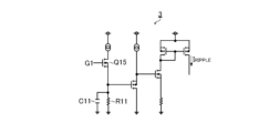
- a gate drive circuit that drives a half bridge in which a high-side transistor to be driven and a low-side transistor to be driven are connected in series between a power supply voltage and a ground potential, a high-side pre-driver configured to drive a gate of the high-side transistor to be driven; a low-side pre-driver configured to drive a gate of the low-side transistor to be driven; Equipped with The high side pre-driver has a first high side transistor and a second high side transistor, The low-side pre-driver includes a third high-side transistor and a fourth high-side transistor, between a first gate signal that turns on the first high-side transistor and a second gate signal that turns on the second high-side transistor; A delay is provided between at least one of a third gate signal that turns on the third high-side transistor and a fourth gate signal that turns on the fourth high-side transistor.
- a power good circuit includes a first output transistor having a first end connected to a power good terminal and a second end connected to a ground potential application end; a resistor for applying a voltage based on the first power supply voltage to the control end of the first output transistor; a first inverter stage configured to use a second power supply voltage as a power supply voltage and to be able to input a control input signal; a second output transistor having a control end connected to an output end of the first inverter stage, a first end connected to the power good terminal, and a second end connected to a ground potential application end; , Equipped with The power good terminal can be pulled up to the second power supply voltage.
- the overcurrent detection circuit includes a first current generation circuit configured to generate a first current corresponding to a current flowing through the second switch, and a first current generating circuit configured to generate a first current corresponding to a current flowing through the second switch, and a current generating circuit configured to generate a first current that is larger than zero at a timing when the second switch is switched from off to on. , a second current generating circuit configured to generate a second current that fluctuates in synchronization with switching of the first switch and the second switch; and a voltage according to the first current and the second current. and a comparator configured to compare the threshold value.
- the switching control circuit disclosed herein includes an overcurrent detection circuit configured as described above, and a control section configured to control the first switch and the second switch.
- the switching power supply device disclosed herein includes a switching control circuit having the above configuration, the first switch, and the second switch.
- the oscillation prevention circuit disclosed in this specification includes a signal line, a first circuit, a capacitor connected to the signal line, and a resistor provided between the signal line and the first circuit. and has.
- the first circuit has two poles.
- the first circuit, the capacitor, and the resistor have two poles and one zero point.
- the switching control circuit disclosed herein includes an oscillation prevention circuit configured as described above, an error amplifier whose output end is connected to the signal line, and a switching element configured to control a switching element based on the output voltage of the error amplifier. and a control section configured to.
- the switching power supply device disclosed herein includes a switching control circuit having the above configuration and the switching element.
- oscillation of the first circuit having two poles can be prevented.
- FIG. 1 is a diagram showing the configuration of a semiconductor device according to a first embodiment of the present disclosure.
- FIG. 2 is a diagram showing a specific example of the configuration of the gate drive circuit.
- FIG. 3 is a diagram showing an example of the configuration of the first high side drive section.
- FIG. 4 is a timing chart showing the operation when the high-side transistor is turned on and the low-side transistor is turned off.
- FIG. 5 is a timing chart showing the operation when the high-side transistor is turned off and the low-side transistor is turned on in the embodiment of the present disclosure.
- FIG. 6 is a diagram showing an example of the configuration of the first low-side drive section.
- FIG. 7 is a diagram showing the configuration of a gate drive circuit according to a second embodiment of the present disclosure.
- FIG. 1 is a diagram showing the configuration of a semiconductor device according to a first embodiment of the present disclosure.
- FIG. 2 is a diagram showing a specific example of the configuration of the gate drive circuit.
- FIG. 3 is
- FIG. 8 is a diagram illustrating a configuration example of a high side gate voltage monitor section.
- FIG. 9 is a diagram showing an example of the configuration of the first low-side drive section.
- FIG. 10 is a timing chart showing the operation when the high-side transistor is turned off and the low-side transistor is turned on in the second embodiment.
- FIG. 11 is a timing chart showing the operation when the high-side transistor is turned off and the low-side transistor is turned on in the embodiment of the present disclosure.
- FIG. 12 is a diagram illustrating the configuration of a semiconductor device according to an exemplary embodiment of the present disclosure.
- FIG. 13 is a diagram showing a part of the internal configuration of the semiconductor device.
- FIG. 14 is a diagram showing an example of the configuration of the preregulator.
- FIG. 15 is a diagram showing the configuration of a power good circuit according to a comparative example.
- FIG. 16 is a timing chart showing the operation of the power good circuit according to the comparative example at the time of starting up the power supply IC.
- FIG. 17 is a diagram showing the configuration of a power good circuit according to the first embodiment of the present disclosure.
- FIG. 18 is a timing chart showing the operation of the power good circuit according to the first embodiment at startup and shutdown of the power supply IC.
- FIG. 19 is a diagram showing the configuration of a power good circuit according to the second embodiment of the present disclosure.
- FIG. 20 is a timing chart showing the operation of the power good circuit according to the second embodiment at startup and shutdown of the power supply IC.
- FIG. 21 is a diagram showing the configuration of a power good circuit according to the third embodiment of the present disclosure.
- FIG. 22 is a timing chart showing the operation of the power good circuit according to the third embodiment at startup and shutdown of the power supply IC.
- FIG. 23 is a diagram showing the overall configuration of the switching power supply device.
- FIG. 24 is a diagram showing the internal configuration of the semiconductor device.
- FIG. 25 is a diagram showing a comparative example of the lower overcurrent detection circuit.
- FIG. 26 is a timing chart showing ideal waveforms of voltages and currents of each part of the switching power supply device.
- FIG. 27 is a timing chart showing actual waveforms of voltages and currents of each part of the switching power supply device.
- FIG. 28 is a diagram showing a first embodiment of the lower overcurrent detection circuit.
- FIG. 29 is a diagram showing a first configuration example of the current generation circuit.
- FIG. 30 is a timing chart showing actual waveforms of voltages and currents at various parts of the switching power supply device having the lower overcurrent detection circuit according to the first embodiment.
- FIG. 31 is a diagram showing a second configuration example of the current generation circuit.
- FIG. 32 is a diagram showing a third configuration example of the current generation circuit.
- FIG. 33 is a diagram showing a fourth configuration example of the current generation circuit.
- FIG. 34 is a diagram showing a fifth configuration example of the current generation circuit.
- FIG. 35A is a diagram showing a modification of the first circuit.
- FIG. 35B is a diagram showing another modification of the first circuit.
- FIG. 36A is a diagram showing a modification of the second circuit.
- FIG. 36B is a diagram showing another modification of the second circuit.
- FIG. 36C is a diagram showing still another modification of the second circuit.
- FIG. 37 is a timing chart showing actual waveforms of voltages and currents at various parts of a switching power supply device having a current generation circuit of the fifth configuration example.
- FIG. 38 is a diagram showing a second embodiment of the lower overcurrent detection circuit.
- FIG. 39 is a timing chart showing actual waveforms of voltages and currents at various parts of the switching power supply device having the lower overcurrent detection circuit according to the second embodiment.
- FIG. 40 is a diagram showing a third embodiment of the lower overcurrent detection circuit.
- FIG. 41 is a diagram showing the overall configuration of a switching power supply device.
- FIG. 42 is a diagram showing the internal configuration of the semiconductor device.
- FIG. 43 is a diagram showing a configuration example of an error amplifier, an upper clamp circuit, and a lower clamp circuit.
- FIG. 44 is a diagram showing the frequency characteristics of the lower clamp circuit.
- FIG. 45 is a diagram showing the frequency characteristics of the upper clamp circuit.
- FIG. 46 is a diagram showing frequency characteristics of the upper clamp circuit, capacitor, and resistor.
- FIG. 47 is a diagram showing an example of the configuration of a differential amplifier.
- MOSFET Metal-Oxide-Semiconductor Field Effect Transistor
- a field-effect transistor consisting of at least three layers: a semiconductor layer, and a P-type, N-type, or intrinsic semiconductor layer. That is, the structure of the gate of the MOS field effect transistor is not limited to the three-layer structure of metal, oxide, and semiconductor.
- the reference voltage refers to a voltage that is constant in an ideal state, and is actually a voltage that may vary slightly due to temperature changes or the like.
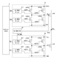
- FIG. 1 is a diagram showing the configuration of a semiconductor device 1 according to a first embodiment of the present disclosure.
- the semiconductor device 1 is a device in which a power supply IC having a DC/DC converter function is packaged. As shown in FIG. 1, the semiconductor device 1 includes a high-side transistor HM, a low-side transistor LM, a gate drive circuit 2, a control logic section 3, and a switch 4 in an integrated manner.
- An inductor L, an output capacitor Cout, and a boot capacitor Cbst are provided outside the semiconductor device 1. These external elements and semiconductor device 1 constitute a step-down DC/DC converter.
- the high-side transistor HM and the low-side transistor LM are both constructed from NMOS transistors (N-channel MOSFETs).
- the drain of the high-side transistor HM is connected to the application terminal of the input voltage Vin.
- the source of the high-side transistor HM is connected to the drain of the low-side transistor LM.
- the source of the low-side transistor LM is connected to a ground potential application terminal. That is, the high-side transistor HM and the low-side transistor LM are connected in series between the input voltage Vin and the ground potential.
- a so-called half bridge is constituted by the high side transistor HM and the low side transistor LM.
- a node Nsw to which the source of the high-side transistor HM and the drain of the low-side transistor LM are connected is connected to one end of the inductor L.
- the other end of the inductor L is connected to one end of the output capacitor Cout.
- the other end of the output capacitor Cout is connected to a ground potential application end.
- An output voltage Vout is generated at one end of the output capacitor Cout.
- the gate drive circuit 2 is a circuit that drives each gate of the high-side transistor HM and the low-side transistor LM, and includes a high-side pre-driver 21 and a low-side pre-driver 22.
- the high-side pre-driver 21 drives the gate of the high-side transistor HM based on the control signal input from the control logic section 3.
- the low-side predriver 22 drives the gate of the low-side transistor LM based on a control signal input from the control logic section 3.
- the input voltage Vin is converted into the output voltage Vout by complementary switching driving of the transistors HM and LM by the pre-drivers 21 and 22.
- the boot capacitor Cbst and switch 4 are used to configure a bootstrap.
- One end of the boot capacitor Cbst is connected to one end of the inductor L.
- the other end of the boot capacitor Cbst is connected to the high side predriver 21.
- the other end of the boot capacitor Cbst is connected via the switch 4 to the application end of the power supply voltage Vcc.
- the power supply voltage Vcc is, for example, an internal voltage generated by an LDO (Low Dropout) based on the input voltage Vin.
- the switch 4 When the high-side transistor HM is off and the low-side transistor LM is on, the switch 4 is turned on and the boot capacitor Cbst is charged. When the high side transistor HM is on and the low side transistor LM is off, the switch 4 is turned off and the boot voltage Vbst generated in the boot capacitor Cbst is supplied to the high side predriver 21. Since the boot voltage Vbst is higher than the input voltage Vin, the high-side transistor HM made of an NMOS transistor can be turned on.
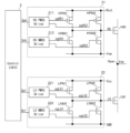
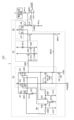
- FIG. 2 is a diagram showing a specific example of the configuration of the gate drive circuit 2.
- the high-side pre-driver 21 includes a first high-side PMOS transistor (P-channel MOSFET) HPM1, a second high-side PMOS transistor HPM2, a first high-side NMOS transistor HNM1, and a second high-side NMOS transistor HNM2.
- the high-side pre-driver 21 includes a first high-side drive section (high-side PMOS drive section) 211 that drives the high-side PMOS transistors HPM1 and HPM2, and a second high-side drive section (high-side drive section) that drives the high-side NMOS transistors HNM1 and HNM2.
- the high side NMOS drive section) 212 is further included.
- the sources of the high-side PMOS transistors HPM1 and HPM2 are connected to the application terminal of the boot voltage Vbst.
- the drains of the high side PMOS transistors HPM1 and HPM2 are connected to the drains of the high side NMOS transistors HNM1 and HNM2.
- the sources of the high-side NMOS transistors HNM1 and HNM2 are connected to the application terminal of the switch voltage Vsw generated at the node Nsw.
- a node to which the drains of the high-side PMOS transistors HPM1 and HPM2 and the drains of the high-side NMOS transistors HNM1 and HNM2 are connected is connected to the gate of the high-side transistor HM.
- the first high-side driving section 211 drives the gates of the high-side PMOS transistors HPM1 and HPM2 by applying gate signals pgHS1 and pgHS2 to the gates of the high-side PMOS transistors HPM1 and HPM2, respectively.
- the second high-side driving section 212 drives the gates of the high-side NMOS transistors HNM1 and HNM2 by applying gate signals ngHS1 and ngHS2 to the gates of the high-side NMOS transistors HNM1 and HNM2, respectively.
- the first high-side drive section 211 outputs the gate signals pgHS1 and pgHS2 at a logic level corresponding to the logic level of the high-side control signal Sph input from the control logic section 3.
- the second high-side drive section 212 outputs the gate signals ngHS1 and ngHS2 at a logic level corresponding to the logic level of the high-side control signal Snh input from the control logic section 3.
- the low-side predriver 22 includes a first low-side PMOS transistor LPM1, a second low-side PMOS transistor LPM2, a first low-side NMOS transistor LNM1, and a second low-side NMOS transistor LNM2.
- the low-side pre-driver 22 includes a first low-side drive section (low-side PMOS drive section) 221 that drives low-side PMOS transistors LPM1 and LPM2, and a second low-side drive section (low-side NMOS drive section) 222 that drives low-side NMOS transistors LNM1 and LNM2. It further has.
- the sources of the low-side PMOS transistors LPM1 and LPM2 are connected to the application terminal of the power supply voltage Vcc.
- the drains of the low-side PMOS transistors LPM1 and LPM2 are connected to the drains of the low-side NMOS transistors LNM1 and LNM2.
- the sources of the low-side NMOS transistors LNM1 and LNM2 are connected to a ground potential application terminal.
- a node to which the drains of the low-side PMOS transistors LPM1 and LPM2 and the drains of the low-side NMOS transistors LNM1 and LNM2 are connected is connected to the gate of the low-side transistor LM.
- the first low-side driving section 221 drives the gates of the low-side PMOS transistors LPM1 and LPM2 by applying gate signals pgLS1 and pgLS2 to the gates of the low-side PMOS transistors LPM1 and LPM2, respectively.
- the second low-side driving section 222 drives the gates of the low-side NMOS transistors LNM1 and LNM2 by applying gate signals ngLS1 and ngLS2 to the gates of the low-side NMOS transistors LNM1 and LNM2, respectively.
- the first low-side drive section 221 outputs the gate signals pgLS1 and pgLS2 at a logic level corresponding to the logic level of the low-side control signal Spl input from the control logic section 3.
- the second low-side drive section 222 outputs the gate signals ngLS1 and ngLS2 at a logic level corresponding to the logic level of the low-side control signal Snl input from the control logic section 3.
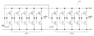
- FIG. 3 is a diagram showing an example of the configuration of the first high side drive section 211.
- the first high-side drive section 211 includes a first high-side gate signal generation section 2111 that generates a gate signal pgHS1 based on a high-side control signal Sph, and a second high-side gate signal generation section 2111 that generates a gate signal pgHS2 based on a high-side control signal Sph. It has a gate signal generation section 2112.
- the first high-side gate signal generation section 2111 is composed of five stages of inverters 211A.
- Each inverter 211A is composed of a PMOS transistor and an NMOS transistor connected in series between the boot voltage Vbst and the switch voltage Vsw.
- the high side control signal Sph is input to the first stage inverter 211A, and the gate signal pgHS1 is output from the final stage inverter 211A.
- the second high side gate signal generation section 2112 is composed of five stages of inverters 211B.
- Each inverter 211B is composed of a PMOS transistor and an NMOS transistor connected in series between the boot voltage Vbst and the switch voltage Vsw.
- the high-side control signal Sph is input to the first-stage inverter 211B, and the gate signal pgHS2 is output from the final-stage inverter 211B.
- inverters 211A and 211B are not limited to five stages.
- the configuration of the second high-side drive unit 212 is the same as that shown in FIG. 3, except that the high-side control signal Sph is replaced with the high-side control signal Snh, and the gate signals pgHS1 and pgHS2 are replaced with gate signals ngHS1 and ngHS2. .
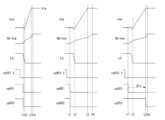
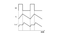
- FIG. 4 is a timing chart showing the operation when the high-side transistor HM is turned on and the low-side transistor LM is turned off.
- FIG. 4 shows the case of normal operation.
- the normal operation is an operation when current flows from the node Nsw to the inductor L side (solid arrow in FIG. 1). Note that FIG. 4 shows three patterns to be described later.
- FIG. 4 waveform examples of the switch voltage Vsw, high side gate voltage HG, low side gate voltage LG, gate signals ngHS1, 2, gate signal pgHS1, and gate signal pgHS2 are shown in order from the top.
- the high-side gate voltage HG (FIG. 2) is the voltage applied to the gate of the high-side transistor HM with reference to the switch voltage Vsw, that is, the Vgs of the high-side transistor HM.
- the low-side gate voltage LG (FIG. 2) is a voltage applied to the gate of the low-side transistor LM with reference to the ground potential, that is, Vgs of the low-side transistor LM.
- the left side of FIG. 4 shows the operation when no delay is provided to the gate signals pgHS1 and pgHS2, as a comparative example with the embodiment of the present disclosure.
- the high side transistor HM is in an off state and the low side transistor LM is in an on state.
- the low-side predriver 22 starts discharging the gate of the low-side transistor LM (timing t1).
- the low side PMOS transistors LPM1 and LPM2 are turned off and the low side NMOS transistors LNM1 and LNM2 are turned on, and the low side gate voltage LG starts to decrease.
- the voltage drop in the low-side transistor LM increases due to the current flowing through the low-side transistor LM, and the switch voltage Vsw decreases.
- the low side gate voltage LG drops to the ground potential (timing t2).
- the gate signals ngHS1 and ngHS2 are switched from high level to low level and the high-side NMOS transistors HNM1 and HNM2 are turned off, the gate signals pgHS1 and pgHS2 are switched from high level to low level. This turns on the high side PMOS transistors HPM1 and HPM2. Therefore, a dead time (simultaneous off period) is provided.
- the levels of the gate signals pgHS1 and pgHS2 switch at timing t1, and the high side gate voltage HG starts rising. From timing t2, the switch voltage Vsw increases as the high side gate voltage HG increases. As the high-side gate voltage HG increases, the on-resistance of the high-side transistor HM decreases, and the voltage drop in the high-side transistor HM decreases, so the switch voltage Vsw increases.
- the switch voltage Vsw reaches the input voltage Vin (timing t3).
- the high side gate voltage HG continues to rise after timing t3 and reaches the boot voltage Vbst at timing t4.
- the operation is as shown on the right side of FIG. 4.
- the gate signal pgHS2 is provided with a delay Dly with respect to the gate signal pgHS1.
- the delay time of the delay Dly is set so that the gate signal pgHS2 switches to low level at timing t3 when the switch voltage Vsw reaches the input voltage Vin.
- the high-side PMOS transistor HPM1 is first turned on by switching the gate signal pgHS1 to low level at timing t1, and then the high-side PMOS transistor HPM2 is turned on by switching the gate signal pgHS2 to low level at timing t3. Therefore, during the period (t2 to t3) in which the switch voltage Vsw increases, only HPM1 of the high-side PMOS transistors HPM1 and HPM2 is in the on state, so the driving ability is suppressed and the slope of the high-side gate voltage HG is reduced. The slew rate of switch Vsw becomes smaller.
- the high side control signal Sph is switched to high level in the first high side drive section 211 having the configuration shown in FIG. 3.
- the gate signal generation units 2111 and 2112 cause switching of the gate signals pgHS1 and pgHS2 to occur with a delay from switching of the high side control signal Sph. Such a delay is caused by the on-resistance of the transistors in the inverters 211A and 211B, and the capacitance caused by the wiring, the gates of the transistors, and the like.
- the size of the NMOS transistor of the first stage inverter 211B is made smaller than the size of the NMOS transistor of the first stage inverter 211A, and the on-resistance is increased. I'm making adjustments.
- the size of the transistor in the later-stage inverters 211A and 211B it is necessary to increase the size of the transistors to ensure driving capability, and it is difficult to adjust the on-resistance, so the size is adjusted in the first-stage inverter. Note that, for example, the size of the transistor in the second-stage inverter in addition to the first-stage inverter may be adjusted.
- FIG. 5 is a timing chart showing the operation when the high-side transistor HM is turned off and the low-side transistor LM is turned on in the embodiment of the present disclosure.
- FIG. 5 shows the case of backflow operation.
- the reverse current operation is an operation when current flows from the inductor L to the node Nsw (broken line arrow in FIG. 1).
- waveform examples of the switch voltage Vsw, high side gate voltage HG, low side gate voltage LG, gate signals ngLS1 and ngLS2, gate signal pgLS1, and gate signal pgLS2 are shown in order from the top. As shown in FIG. 5, a delay is provided for gate signals pgLS1 and pgLS2.
- the high-side transistor HM is in the on state and the low-side transistor LM is in the off state.
- the high-side predriver 21 starts discharging the gate of the high-side transistor HM (timing t11).
- the high side PMOS transistors HPM1 and HPM2 are turned off and the high side NMOS transistors HNM1 and HNM2 are turned on, and the high side gate voltage HG starts to decrease.
- the voltage drop at the high-side transistor HM increases due to the current flowing through the high-side transistor HM, and the switch voltage Vsw increases.
- the high side gate voltage HG decreases to the switch voltage Vsw (timing t12).
- the gate signal pgLS1 is switched from high level to low level, so that the low-side PMOS Transistor LPM1 is turned on. Therefore, a dead time is provided.
- the level of the gate signal pgLS1 switches at timing t11, and the low-side gate voltage LG starts to rise. From timing t12, as the low side gate voltage LG increases, the switch voltage Vsw decreases. As the low-side gate voltage LG increases, the on-resistance of the low-side transistor LM decreases, and the voltage drop in the low-side transistor LM decreases, so the switch voltage Vsw decreases.
- the switch voltage Vsw reaches the ground potential (timing t13).
- the gate signal pgLS2 is switched to low level. This turns on the low-side PMOS transistor LPM2.
- the low-side gate voltage LG continues to rise after timing t13, and reaches the power supply voltage Vcc at timing t14.
- the low-side PMOS transistor LPM1 is first turned on by switching the gate signal pgLS1 to low level at timing t11, and then the low-side PMOS transistor LPM2 is turned on by switching the gate signal pgLS2 to low level at timing t13. Therefore, during the period (t12 to t13) in which the switch voltage Vsw decreases, only LPM1 of the low-side PMOS transistors LPM1 and LPM2 is in the on state, so the driving ability is suppressed, the slope of the low-side gate voltage LG is made small, and the switch Vsw slew rate becomes smaller.
- FIG. 6 is a diagram showing an example of the configuration of the first low-side drive section 221.
- the first low-side drive section 221 includes a first low-side gate signal generation section 2211 that generates a gate signal pgLS1 based on a low-side control signal Spl, and a second low-side gate signal generation section 2212 that generates a gate signal pgLS2 based on a low-side control signal Spl. and has.
- the first low-side gate signal generation section 2211 is composed of five stages of inverters 221A.
- Each inverter 221A is composed of a PMOS transistor and an NMOS transistor connected in series between power supply voltage Vcc and ground potential.
- the low-side control signal Spl is input to the first-stage inverter 221A, and the gate signal pgLS1 is output from the final-stage inverter 221A.
- the second low-side gate signal generation section 2212 is composed of five stages of inverters 221B.
- Each inverter 221B is composed of a PMOS transistor and an NMOS transistor connected in series between power supply voltage Vcc and ground potential.
- the low-side control signal Spl is input to the first-stage inverter 221B, and the gate signal pgLS2 is output from the final-stage inverter 221B.
- inverters 221A and 221B are not limited to five stages.
- the configuration of the second low-side drive section 222 is the same as that shown in FIG. 6, in which the low-side control signal Spl is replaced with the low-side control signal Snl, and the gate signals pgLS1 and pgLS2 are replaced with gate signals ngLS1 and ngLS2.
- the size of the NMOS transistor of the first stage inverter 221B is made smaller than the size of the NMOS transistor of the first stage inverter 221A, and the on-resistance is adjusted. are doing.
- the size of the transistor in the later-stage inverters 221A and 221B it is necessary to increase the size of the transistors to ensure driving capability, and it is difficult to adjust the on-resistance, so the size is adjusted in the first-stage inverter. Note that, for example, the size of the transistor in the second-stage inverter in addition to the first-stage inverter may be adjusted.
- FIG. 7 is a diagram showing a configuration of a gate drive circuit 2 according to a second embodiment of the present disclosure.
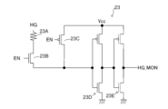
- the gate drive circuit 2 shown in FIG. 7 further includes a high-side gate voltage monitor section 23, unlike the configuration of the first embodiment (FIG. 2) described above.
- a delay is provided to the gate signals pgHS1 and pgHS2 due to the configuration of the first high-side drive section 211 in the high-side predriver 21.
- FIG. 8 is a diagram showing an example of the configuration of the high side gate voltage monitor section 23.
- the high side gate voltage monitor section 23 shown in FIG. 8 includes a resistor 23A, switches 23B and 23C, and inverters 23D and 23E.
- Switch 23B is composed of an NMOS transistor.
- the switch 23C is composed of a PMOS transistor.
- resistor 23A One end of the resistor 23A is connected to the gate of the high-side transistor HM.
- the other end of resistor 23A is connected to the input end of inverter 23D via switch 23B.
- Inverters 23D and 23E include a PMOS transistor and an NMOS transistor connected in series between power supply voltage Vcc and ground potential.
- the output end of inverter 23D is connected to the input end of inverter 23E.
- a switch 23C is connected between the application end of the power supply voltage Vcc and the input end of the inverter 23D.
- the switches 23B and 23C are controlled by an enable signal EN.
- EN When the enable signal EN is at a low level, the switch 23B is turned off, the switch 23C is turned on, and the PMOS transistors of the inverters 23D and 23E are turned off. As a result, the high side gate voltage monitor section 23 becomes disabled.
- the enable signal EN when the enable signal EN is at a high level, the switch 23B is on, the switch 23C is off, and the high-side gate voltage monitor section 23 is enabled.
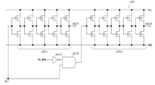
- FIG. 9 is a diagram showing a configuration example of the first low-side drive section 221 according to the second embodiment.
- the first low-side drive section 221 shown in FIG. 9 includes a first low-side gate signal generation section 2211 that generates the gate signal pgLS1 based on the low-side control signal Spl, and a second low-side gate that generates the gate signal pgLS2 based on the low-side control signal Spl. It has a signal generation section 2212.
- the low side drive sections 2211 and 2212 have the same configuration as that shown in FIG. 6 described above.
- the first low-side drive section 221 further includes an inverter 221C and an AND circuit 221D.
- a monitor signal HG_MOM is input to the inverter 221C.
- the output of the inverter 221C is input to one input terminal of the AND circuit 221C, and the low-side control signal Spl is input to the other input terminal.
- the output of the AND circuit 221D is input to the second low-side gate signal generation section 2212.
- the gate signal pgLS1 when the low-side control signal Spl rises to a high level, the gate signal pgLS1 first falls to a low level. Then, when the monitor signal HG_MOM falls to a low level, the output of the AND circuit 221D rises to a high level, and the gate signal pgLS2 falls to a low level. Therefore, it is possible to provide a delay in the gate signal pgLS2 with respect to the gate signal pgLS1.
- FIG. 10 is a timing chart showing the operation when the high-side transistor HM is turned off and the low-side transistor LM is turned on in the second embodiment.
- FIG. 10 shows the case of backflow operation.
- the difference between the timing chart shown in FIG. 10 and FIG. 5 (first embodiment) is the monitor signal HG_MON.
- the low-side control signal Spl is switched to high level
- the gate signal pgLS1 is switched to low level at timing t11.
- the high-side gate voltage monitor section 23 switches the monitor signal HG_MON to a low level. Then, the gate signal pgLS2 is switched to low level. In this manner, also in this embodiment, since a delay is provided to the gate signals pgLS1 and pgHS2, similarly to the first embodiment, it is possible to suppress the self-turn-on of the high-side transistor HM and suppress the decrease in efficiency.
- FIG. 11 is a timing chart showing the operation when the high-side transistor HM is turned off and the low-side transistor LM is turned on in the embodiment of the present disclosure.
- FIG. 11 shows the case of normal operation.
- the left side of FIG. 11 shows the operation in the first embodiment.
- the high-side predriver 21 starts discharging the gate of the high-side transistor HM, and the high-side gate voltage HG starts to decrease.
- the switch voltage Vsw starts decreasing from timing t21.
- the high-side gate voltage HG decreases, the on-resistance of the high-side transistor HM increases, the voltage drop in the high-side transistor HM increases, and the switch voltage Vsw decreases.
- the gate signal pgLS1 is switched to low level.
- the low level PMOS transistor LPM1 is turned on, and the low side gate voltage LG starts to rise.
- the gate signal pgLS2 is switched to low level at timing t23.
- the low-level PMOS transistor LPM2 is turned on, and the low-side gate voltage LG continues to rise further and reaches the power supply voltage Vcc (timing t24).
- the low-side gate voltage LG starts rising after the switch voltage Vsw transitions, so the slope of the low-side gate voltage LG has no relation to the slew rate of the switch voltage Vsw. Therefore, according to the first embodiment, since the gate signal pgLS2 is delayed by a certain amount with respect to pgLS1, the time (t22 to t24) for the low side gate voltage LG to reach the power supply voltage Vcc becomes longer, and the efficiency decreases. . Furthermore, since the rise in the low-side gate voltage LG is delayed, the rise in the switch voltage Vsw is delayed.
- the right side of FIG. 11 shows the operation in the second embodiment.
- the monitor signal HG_MON is switched to low level at timing t22 when the switch voltage Vsw becomes close to the ground potential. Therefore, the gate signal pgLS2 is switched to a low level with almost no delay relative to pgLS1.
- the time (t22 to t24) until the low-side gate voltage LG reaches the power supply voltage Vcc is shortened, and a decrease in efficiency is suppressed.
- the present disclosure can be applied not only to a DC/DC converter but also to driving a transistor in an inverter circuit that performs DC/AC conversion.
- the gate drive circuit (2) A gate drive circuit that drives a half bridge in which a high-side transistor (HM) to be driven and a low-side transistor (LM) to be driven are connected in series between a power supply voltage (Vin) and a ground potential, a high-side pre-driver (21) configured to drive the gate of the high-side transistor to be driven; a low-side predriver (22) configured to drive the gate of the low-side transistor to be driven; Equipped with The high-side pre-driver includes a first high-side transistor (HPM1) and a second high-side transistor (HPM2), The low-side pre-driver includes a third high-side transistor (LPM1) and a fourth high-side transistor (LPM2), between a first gate signal (pgHS1) that turns on the first high-side transistor and a second gate signal (pgHS2) that turns on the second high-side transistor; A delay is provided between at least one of the third gate signal
- the high-side predriver (21) generates the first gate signal (pgHS1) and the second gate signal (pgHS2) based on the high-side control input signal (Sph). It is also possible to have a configuration including a high side drive section (211) configured as follows (second configuration).
- the high side drive section (211) a first high side gate signal generation section (2111) configured to have a plurality of first inverters (211A) and generate the first gate signal (pgHS1); a second high side gate signal generation section (2112) configured to have a plurality of second inverters (211B) and generate the second gate signal (pgHS2); has At least one of the second inverters in the second high-side gate signal generation section may have a transistor size smaller than at least one of the first inverters in the first high-side gate signal generation section ( (3rd configuration).
- the second inverter (211B) at the first stage in the second high side gate signal generation section (2112) is connected to the second inverter (211B) at the first stage in the first high side gate signal generation section (2111). It is also possible to adopt a configuration in which the size of the transistor is smaller than one inverter (211A) (fourth configuration).
- the low side predriver (22) generates the third gate signal (pgLS1) and the fourth gate signal (pgLS2) based on the low side control input signal (Spl). ) (fifth configuration).
- the low side drive section (221) a first low-side gate signal generation section (2211) configured to have a plurality of third inverters (221A) and generate the third gate signal (pgLS1); a second low-side gate signal generation section (2212) configured to have a plurality of fourth inverters (221B) and generate the fourth gate signal (pgLS2); has At least one of the fourth inverters in the second low-side gate signal generation section may have a transistor size smaller than at least one of the third inverters in the first low-side gate signal generation section (sixth configuration).
- the fourth inverter (221B) at the first stage in the second low-side gate signal generation section (2212) is the third inverter at the first stage in the first low-side gate signal generation section (2211).
- (221A) may be configured in which the size of the transistor is smaller (seventh configuration).
- the gate voltage (HG) of the high-side transistor to be driven (HM) is at a low level
- the fourth gate signal (pgLS2) may be generated based on the monitor signal (HG_MON) output from the monitor unit (eighth configuration).
- the monitor section (23) includes a resistor (23A) having a first end connected to the gate of the driven transistor (HM), and a second end connected to the resistor.
- Inverter stages (23D, 23E) having input terminals may also be used (ninth configuration).
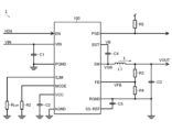
- FIG. 12 is a diagram showing the configuration of a semiconductor device 1 according to an exemplary embodiment of the present disclosure.
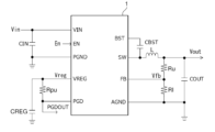
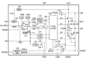
- the semiconductor device 1 is a device in which a power supply IC having a DC/DC converter function is packaged. As shown in FIG. 12, the semiconductor device 1 has a VIN (input voltage) terminal, an EN (enable) terminal, a PGND (power ground) terminal, and a VREG (constant voltage) terminal as external terminals for establishing electrical connection with the outside. voltage) terminal, PGD (power good) terminal, BST (bootstrap) terminal, SW (switch) terminal, FB (feedback) terminal, and AGND (analog ground) terminal.
- An input voltage Vin can be applied to the VIN terminal.
- a ground potential can be applied to the PGND terminal.
- An input capacitor CIN is connected between an end to which an input voltage Vin is applied and an end to which a ground potential is applied.
- the semiconductor device 1 has an upper switching element and a lower switching element (not shown). Both the upper switching element and the lower switching element are configured by NMOS transistors (N-channel MOSFETs (metal-oxide-semiconductor field-effect transistors)). The upper switching element and the lower switching element are connected in series between the VIN terminal and the PGND terminal. A node to which the upper switching element and the lower switching element are connected is connected to an SW terminal.
- NMOS transistors N-channel MOSFETs (metal-oxide-semiconductor field-effect transistors)
- the SW terminal is connected to one end of the inductor L.
- the other end of the inductor L is connected to one end of the output capacitor COUT.
- the other end of the output capacitor COUT and the AGND terminal are connected to a ground potential application end.
- an output voltage Vout is generated.
- Voltage dividing resistors Ru and Rl are connected in series between the other end of the inductor L and the AGND terminal.
- a node to which the voltage dividing resistors Ru and Rl are connected is connected to the FB terminal.
- a feedback voltage Vfb generated by dividing the output voltage Vout by voltage dividing resistors Ru and Rl is applied to the FB terminal.
- the semiconductor device 1 has a feedback control section (not shown).
- the feedback control section controls switching of the upper switching element and the lower switching element based on the feedback voltage Vfb. Thereby, the output voltage Vout is controlled to a desired voltage value.
- the feedback control section includes an error amplifier, a control logic section, a driver, and the like.
- a bootstrap capacitor CBST is connected between the BST terminal and the SW terminal. By charging the bootstrap capacitor CBST, the upper switching element formed by the NMOS transistor can be turned on.
- the upper switching element, the lower switching element, and the feedback control section are integrated into the power supply IC and provided in the semiconductor device 1.
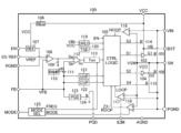
- FIG. 13 is a diagram showing a part of the internal configuration of the semiconductor device 1. As shown in FIG. 13, the semiconductor device 1 includes a preregulator (PREREG) 2, a reference voltage generation section 3, and a regulator (REG) 4, and these components are integrated into the power supply IC.
- PREREG preregulator
- REG regulator
- the preregulator 2 generates a first power supply voltage Vprereg based on the input voltage Vin applied to the VIN terminal.
- the first power supply voltage Vprereg is a constant voltage.
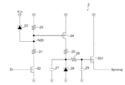
- FIG. 14 is a diagram showing a configuration example of the preregulator 2.
- the preregulator 2 includes voltage dividing resistors 20 and 21, an NMOS transistor 22, a Zener diode 23, a PMOS transistor (P-channel MOSFET) 24, a resistor 25, a Zener diode 26, a capacitor 27, and a resistor 28. , a capacitor 29, and an NMOS transistor 201.
- the voltage dividing resistors 20 and 21 are connected in series between the application terminal of the input voltage Vin and the drain of the NMOS transistor 22.
- the source of the NMOS transistor 22 is connected to a ground potential application terminal.
- the gate of the NMOS transistor 22 is driven by an enable signal En applied to the EN terminal (FIG. 13).
- the anode of the Zener diode 23 is connected to a node N20 to which the voltage dividing resistors 20 and 21 are connected.
- the cathode of the Zener diode 23 is connected to the application terminal of the input voltage Vin. Zener diode 23 clamps the voltage at node N20 to suppress excessive drop.
- the node N20 is connected to the gate of the PMOS transistor 24.
- the source of the PMOS transistor 24 is connected to the application terminal of the input voltage Vin.
- a drain of the PMOS transistor 24 is connected to one end of a resistor 25.
- the other end of the resistor 25 is connected to the cathode of a Zener diode 26.
- the anode of the Zener diode 26 is connected to a ground potential application terminal.
- the cathode of the Zener diode 26 is connected to one end of the capacitor 27.
- the other end of the capacitor 27 is connected to a ground potential application end.
- a cathode of the Zener diode 26 is connected to one end of a resistor 28.
- the other end of the resistor 28 is connected to one end of a capacitor 29.
- the other end of the capacitor 29 is connected to a ground potential application end.
- the resistor 28 and capacitor 29 constitute a low pass filter.
- the other end of the resistor 28 is connected to the gate of the NMOS transistor 201.
- the drain of the NMOS transistor 201 is connected to the application terminal of the input voltage Vin.
- a first power supply voltage Vprereg is generated at the source of the NMOS transistor 201.
- the NMOS transistor 22 is in the on state, a voltage obtained by dividing the input voltage Vin by the voltage dividing resistors 20 and 21 is generated at the node N20, and the PMOS transistor 24 is in the on state.
- Vz is the Zener voltage of the Zener diode 26
- Vgs is the gate-source voltage of the NMOS transistor 201.
- the reference voltage generation section 3 generates the reference voltage Vref based on the first power supply voltage Vprereg.
- the reference voltage generation section 3 is configured by, for example, a bandgap reference.
- the reference voltage Vref is used, for example, to generate the second power supply voltage Vreg in the regulator 4.
- the regulator 4 generates a second power supply voltage Vreg based on the input voltage Vin.
- the regulator 4 is configured by, for example, an LDO (Low Dropout).
- the reference voltage Vref is input to the error amplifier in the LDO.
- a second power supply voltage Vreg is generated at the VREG terminal. As shown in FIG. 12, the VREG terminal is connected to the capacitor CREG.
- the second power supply voltage Vreg is supplied to each part of the power supply IC.
- the second power supply voltage Vreg is supplied, for example, to a power good circuit 5, which will be described later.
- the first power supply voltage Vprereg and the second power supply voltage Vreg may have the same voltage value or may have different voltage values.
- the semiconductor device 1 includes a power good circuit 5.
- the power good circuit 5 is integrated into the power supply IC.
- the power good circuit 5 is connected between the PGD terminal and the end to which a ground potential is applied. As shown in FIG. 12, a pull-up resistor Rpu is connected between the PGD terminal and the VREG terminal. That is, the PGD terminal is pulled up to the second power supply voltage Vreg.
- the power good circuit 5 has a switch (output transistor) not shown in FIG. 13 connected between the PGD terminal and the end to which a ground potential is applied.
- the switch When the switch is on, the flag signal PGDOUT (FIG. 12) output from the PGD terminal is at a low level, and when the switch is off, the flag signal PGDOUT is at a high level.
- the power good circuit 5 detects this based on the feedback voltage Vfb generated at the FB terminal and turns it high.
- a level flag signal PGDOUT is output.
- the flag signal PGDOUT can notify the outside that the output voltage Vout output from the power supply circuit (DC/DC converter) has risen normally.
- FIG. 15 is a diagram showing the configuration of a power good circuit 5 according to a comparative example.
- a comparative example will be described for comparison with the embodiment of the present disclosure described below. The issues will become clear by explaining comparative examples.
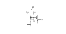
- the power good circuit 5 shown in FIG. 15 includes an output transistor MA and inverters IVA and IVB.
- Output transistor MA is composed of an NMOS transistor.
- the drain of output transistor MA is connected to the PGD terminal.
- the source of output transistor MA is connected to a ground potential application terminal.
- the input end of the inverter IVA is connected to the application end of the control input signal PGDIN.
- the control input signal PGDIN is a signal generated inside the power good circuit 5.
- the output end of inverter IVA is connected to the input end of inverter IVB.
- the output terminal of inverter IVB is connected to the gate of output transistor MA.
- the control input signal PGDIN is logically inverted by the inverters IVA and IVB and input to the gate of the output transistor MA.
- Inverters IVA and IVB each have a PMOS transistor and an NMOS transistor (not shown).
- a source of the PMOS transistor is connected to an application terminal of the second power supply voltage Vreg.
- the drain of the PMOS transistor is connected to the drain of the NMOS transistor.
- the source of the NMOS transistor is connected to a ground potential application terminal.
- a gate of the PMOS transistor and a gate of the NMOS transistor are connected to an input terminal of an inverter.
- a node to which the drain of the PMOS transistor and the drain of the NMOS transistor are connected is connected to the output end of the inverter. That is, inverters IVA and IVB use the second power supply voltage Vreg as a power supply voltage.
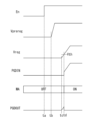
- FIG. 16 is a timing chart showing the operation of the power good circuit 5 according to the comparative example at the time of starting up the power supply IC.
- the enable signal En the first power supply voltage Vprereg, the second power supply voltage Vreg, the control input signal PGDIN, the on/off state of the output transistor MA, and the flag signal PGDOUT are shown in order from the top.
- the enable signal En switches from a low level indicating disable to a high level indicating enable (timing ta). Then, the preregulator 2 is activated and the first power supply voltage Vprereg starts rising (timing tb). Thereafter, the reference voltage generation section 3 is activated, and the regulator 4 is activated by the reference voltage Vref. At this time, the second power supply voltage Vreg starts rising (timing tc). That is, the preregulator 2, the reference voltage generation section 3, and the regulator 4 are activated in this order.
- Threshold voltage Vth is the threshold voltage of inverters IVA and IVB as well as the threshold voltage of output transistor MA.
- the control input signal PGDIN becomes high level, a high level signal is input to the gate of the output transistor MA, and the output transistor MA is turned on. As a result, the flag signal PGDOUT falls to low level.
- the power good circuit 5 has a problem in that the output transistor MA cannot be turned on when the power supply IC is started, and the flag signal PGDOUT rises.
- embodiments of the present disclosure described below are implemented.
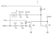
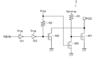
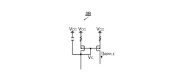
- FIG. 17 is a diagram showing the configuration of the power good circuit 5 according to the first embodiment of the present disclosure.
- the power good circuit 5 shown in FIG. 17 includes an output transistor M1, an output transistor M2, inverters IV1 to IV4, pull-up resistors R1 and R2, and a level shift circuit 51.
- the output transistor M1 is composed of an NMOS transistor.
- the drain of the output transistor M1 is connected to the PGD terminal.
- the source of the output transistor M1 is connected to a ground potential application terminal.
- a pull-up resistor R1 is connected between the gate of the output transistor M1 and the terminal to which the first power supply voltage Vprereg is applied.
- the input terminal of the level shift circuit 51 is connected to the application terminal of the control input signal PGDIN.
- the output terminal of level shift circuit 51 is connected to the input terminal of inverter IV3.
- the output terminal of inverter IV3 is connected to the input terminal of inverter IV4.
- the output terminal of inverter IV4 is connected to the gate of output transistor M1.
- the level shift circuit 51 converts the level of the control input signal PGDIN from the second power supply voltage Vreg to the first power supply voltage Vprereg.
- the level-converted control input signal PGDIN is logically inverted by each of the inverters IV3 and IV4, and is input to the gate of the output transistor M1.
- Inverters IV3 and IV4 have the same configuration as inverters IVA and IVB according to the comparative example described above, except that the first power supply voltage Vprereg is used as the power supply voltage. That is, inverters IV3 and IV4 include a PMOS transistor and an NMOS transistor (not shown).
- the drain of the output transistor M2 is connected to the PGD terminal.
- the source of the output transistor M2 is connected to a ground potential application terminal.
- the input end of the inverter IV1 is connected to the application end of the control input signal PGDIN.
- the output terminal of inverter IV1 is connected to the input terminal of inverter IV2.
- the output terminal of inverter IV2 is connected to the gate of output transistor M2.
- the inverters IV1 and IV2 use the second power supply voltage Vreg as the power supply voltage, and have the same configuration as the inverters IVA and IVB according to the comparative example described above.
- a pull-up resistor R2 is connected between the gate of the output transistor M2 and the application terminal of the second power supply voltage Vreg.
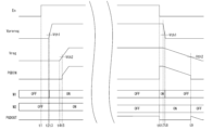
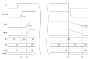
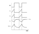
- FIG. 18 is a timing chart showing the operation of the power good circuit 5 according to the first embodiment during startup and shutdown of the power supply IC.
- the enable signal En the first power supply voltage Vprereg, the second power supply voltage Vreg, the control input signal PGDIN, the on/off states of the output transistors M1 and M2, and the flag signal PGDOUT are shown in order from the top.
- the enable signal En switches from low level to high level (timing t1). Then, the first power supply voltage Vprereg starts rising (timing t2). Then, the first power supply voltage Vprereg reaches the threshold voltage Vth1 (timing t3).
- Threshold voltage Vth1 is the threshold voltage of output transistor M1 as well as the threshold voltages of inverters IV3 and IV4.
- the first power supply voltage Vprereg is applied to the gate of the output transistor M1 via the pull-up resistor R1, thereby switching the output transistor M1 from the off state to the on state. .
- the level shift circuit 51 when the second power supply voltage Vreg is at a low level (lower than the threshold voltage Vth2), the level shift circuit 51 outputs a high level signal as an initial value. Until the first power supply voltage Vprereg reaches the threshold voltage Vth1, the outputs of the inverters IV3 and IV4 are logically undefined, but when the first power supply voltage Vprereg reaches the threshold voltage Vth1, the output of the inverter IV4 is determined to be at a high level. The output transistor M1 is turned on.
- the outputs of the inverters IV3 and IV4 become logically undefined, but the pull-up resistor R1 allows the first power supply voltage Vprereg to reach the output transistor.
- the voltage level at the gate of output transistor M1 is determined.
- the second power supply voltage Vreg starts rising (timing t4). Then, the second power supply voltage Vreg reaches the threshold voltage Vth2 (timing t5).
- Threshold voltage Vth2 is the threshold voltage of output transistor M2 as well as the threshold voltages of inverters IV1 and IV2.
- the control input signal PGDIN is at a low level, and the outputs of the inverters IV1 and IV2 have an undefined logic. Further, at this time, the second power supply voltage Vreg is applied to the gate of the output transistor M2 via the pull-up resistor R2, but the output transistor M2 is in an off state.
- the output transistor M1 is already turned on by the first power supply voltage Vprereg. This prevents the flag signal PGDOUT output from the PGD terminal from rising.
- the pull-up resistor R2 that pulls up the gate of the output transistor M2 to the second power supply voltage Vreg does not necessarily need to be provided. However, by providing the pull-up resistor R2, even when the output of the inverter IV2 has an undefined logic, the second power supply voltage Vreg can be applied to the gate of the output transistor M2 via the pull-up resistor R2, and the output transistor M2 The voltage level of the gate can be determined.
- the control input signal PGDIN is switched from high level to low level.
- the level of the gates of the output transistors M1 and M2 becomes low level, and both the output transistors M1 and M2 are turned off.
- the flag signal PGDOUT switches from low level to high level.
- the enable signal En falls from high level to low level (timing t6).
- the output voltage Vout falls and the control input signal PGDIN switches from low level to high level.
- both output transistors M1 and M2 are turned on from the off state. Therefore, the flag signal PGDOUT switches from high level to low level.
- the first power supply voltage Vprereg and the second power supply voltage Vreg start falling (timing t7). Since the capacitor CREG is connected to the VREG terminal, the second power supply voltage Vreg falls more slowly than the first power supply voltage Vprereg.
- the output transistor M1 When the first power supply voltage Vprereg falls below the threshold voltage Vth1, the output transistor M1 is turned off (timing t8). At this time, since the second power supply voltage Vreg is equal to or higher than the threshold voltage Vth2, the output transistor M2 is in an on state. Therefore, the flag signal PGDOUT is maintained at a low level.
- the control input signal PGDIN switches from high level to low level (timing t9). This turns the output transistor M2 off.
- both output transistors M1 and M2 are in an off state.
- the output transistors M1 and M2 can be controlled in a state where at least one of the first power supply voltage Vprereg and the second power supply voltage Vreg is activated (period from timing t3 to t9).
- FIG. 19 is a diagram showing the configuration of a power good circuit 5 according to the second embodiment of the present disclosure.
- the power good circuit 5 shown in FIG. 19 further includes a control transistor M3 compared to the configuration according to the first embodiment (FIG. 17). Note that in the configuration shown in FIG. 19, the level shift circuit 51 and inverters IV3 and IV4 are not provided.
- the control transistor M3 is composed of an NMOS transistor.
- the drain of control transistor M3 is connected to the gate of output transistor M1.
- the source of the control transistor M3 is connected to a ground potential application terminal.
- a gate of the control transistor M3 is connected to an application terminal of the second power supply voltage Vreg.
- FIG. 20 is a timing chart showing the operation of the power good circuit 5 according to the second embodiment during startup and shutdown of the power supply IC.
- the enable signal En the first power supply voltage Vprereg, the second power supply voltage Vreg, the control input signal PGDIN, the on/off states of the output transistors M1, M2 and the control transistor M3, and the flag signal PGDOUT are shown. .
- the first power supply voltage Vprereg reaches the threshold voltage Vth1 (timing t11)
- the first power supply voltage Vprereg is applied to the gate of the output transistor M1 via the pull-up resistor R1, and the output transistor M1 is switched from an off state to an on state.
- both the output transistor M2 and the control transistor M3 are in an off state.
- the output transistor M2 and the control transistor M3 are switched from the off state to the on state. Since the control transistor M3 is turned on, the output transistor M1 is turned off.
- the output transistor M1 since the output transistor M1 is in the on state until the second power supply voltage Vreg reaches the threshold voltage Vth2, it is possible to avoid raising the flag signal PGDOUT. Furthermore, since the output transistor M1 is switched from the on state to the off state, the flag signal PGDOUT is subsequently controlled by the output transistor M2. That is, in the present embodiment, the output transistor M1 prioritizes setting the flag signal PGDOUT to a low level at the time of startup by pulling up the flag signal PGDOUT to the first power supply voltage Vprereg using the pull-up resistor R1.
- the enable signal En switches from high level to low level (timing t13).
- the output voltage Vout falls and the control input signal PGDIN switches from low level to high level.
- the output transistor M2 is turned on from the off state. Therefore, the flag signal PGDOUT switches from high level to low level.
- both the output transistor M2 and the control transistor M3 are switched from the on state to the off state. As a result, both output transistors M1 and M2 are turned off.
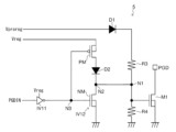
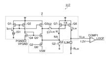
- FIG. 21 is a diagram showing the configuration of a power good circuit 5 according to the third embodiment of the present disclosure.
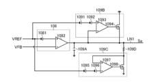
- the power good circuit 5 shown in FIG. 21 includes an output transistor M1, voltage dividing resistors R3 and R4, inverters IV11 and IV12, and diodes D1 and D2. That is, in this embodiment, there is one output transistor.
- the voltage dividing resistors R3 and R4 are connected in series between the application end of the first power supply voltage Vprereg and the application end of the ground potential.
- a node N1 to which the voltage dividing resistors R3 and R4 are connected is connected to the gate of the output transistor M1.
- the input end of the inverter IV11 is connected to the application end of the control input signal PGDIN.
- the output terminal of inverter IV11 is connected to the input terminal of inverter IV12.
- the inverter IV11 uses the second power supply voltage Vreg as the power supply voltage, and has the same configuration as the above-mentioned inverter IV1.
- Inverter IV12 includes a PMOS transistor PM and an NMOS transistor NM.
- a source of the PMOS transistor PM is connected to an application terminal of the second power supply voltage Vreg.
- the drain of the PMOS transistor PM is connected to the drain of the NMOS transistor NM.
- the source of the NMOS transistor NM is connected to a ground potential application terminal.
- a node N3 to which the gate of the PMOS transistor PM and the gate of the NMOS transistor NM are connected serves as an input terminal. Further, a node N2 to which the drain of the PMOS transistor PM and the drain of the NMOS transistor NM are connected serves as an output terminal, and the output terminal is connected to the node N1.
- the anode of the diode D1 is connected to the application terminal of the first power supply voltage Vprereg.
- a cathode of the diode D1 is connected to one end of a voltage dividing resistor R3.
- the anode of diode D2 is connected to the drain of PMOS transistor PM.
- the cathode of diode D2 is connected to node N2.
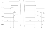
- FIG. 22 is a timing chart showing the operation of the power good circuit 5 according to the third embodiment during startup and shutdown of the power supply IC.
- the enable signal En the first power supply voltage Vprereg, the second power supply voltage Vreg, the control input signal PGDIN, the on/off state of the output transistor M1, and the flag signal PGDOUT are shown in order from the top.
- the enable signal En switches from low level to high level
- the first power supply voltage Vprereg starts rising and reaches the threshold voltage Vth11 (timing t21).
- a voltage obtained by dividing the first power supply voltage Vprereg by the voltage dividing resistors R3 and R4 is applied to the gate of the output transistor M1.
- the output transistor M1 is switched from the off state to the on state.
- the control input signal PGDIN since the control input signal PGDIN is at a low level, the outputs of the inverters IV11 and IV12 are logically undefined.
- Threshold voltage Vth2 is the threshold voltage of output transistor M1, and also the threshold voltage of inverters IV11 and IV12.
- the diode D2 can block the path from the node N1 to the application terminal of the second power supply voltage Vreg, which is at the ground potential level, via the PMOS transistor PM.
- the enable signal En switches from high level to low level (timing t23).
- the output voltage Vout falls and the control input signal PGDIN switches from low level to high level.
- the output transistor M1 is turned on from the off state. Therefore, the flag signal PGDOUT switches from high level to low level.
- the first power supply voltage Vprereg falls to the ground potential. Even if the first power supply voltage Vprereg is at the ground potential, the output of the inverter IV12 is at a high level, so the output transistor M1 is maintained in the on state. At this time, the path from the node N1 to the application end of the first power supply voltage Vprereg, which is at the level of the ground potential, via the voltage dividing resistor R3 can be cut off by the diode D1.
- the power good circuit (5) includes: a first output transistor (M1) having a first end connected to a power good terminal (PGD) and a second end connected to a ground potential application end; a resistor (R1) for applying a voltage based on the first power supply voltage (Vprereg) to the control end of the first output transistor; a first inverter stage (IV1, IV2) configured to use a second power supply voltage (Vreg) as a power supply voltage and to be able to input a control input signal (PGDIN); a second output transistor having a control end connected to the output end of the first inverter stage, a first end connected to the power good terminal, and a second end connected to the ground potential application end ( M2) and Equipped with The power good terminal is configured to be able to be pulled up to the second power supply voltage (first configuration).
- the resistor is a voltage dividing resistor (R3, R4) connected in series between the first power supply voltage (Vprereg) application end and the ground potential application end;
- the connection node (N1) of the voltage dividing resistor may be connected to the control end of the first output transistor (M1) (second configuration).
- the first output transistor (M1) and the second output transistor (M1) are the same transistor, a first diode (D1) for blocking a path from the connection node (N1) to the application end of the first power supply voltage (Vprereg) via the voltage dividing resistor (R3);
- the configuration may include a second diode (D2) for cutting off a path from the connection node to the application terminal of the second power supply voltage (Vreg) via the first inverter stage (IV12). 3 configuration).
- the resistor is a first pull-up resistor (R1) connected between an application terminal of the first power supply voltage (Vprereg) and a control terminal of the first output transistor (M1). ) (fourth configuration).
- the first output transistor (M1) and the second output transistor (M2) may be separate transistors (fifth configuration).
- the configuration includes a second pull-up resistor (R2) connected between the control end of the second output transistor (M2) and the application end of the second power supply voltage (Vreg). (sixth configuration).
- a level shift circuit ( 51) and A second inverter stage (IV3, IV4) provided between the output end of the level shift circuit and the control end of the first output transistor (M1) and using the first power supply voltage as a power supply voltage. (seventh configuration).
- the first terminal connected to the control terminal of the first output transistor (M1), the second terminal connected to the application terminal of the ground potential, and the second power supply voltage (Vreg ) (eighth configuration).
- a semiconductor device (1) includes a power good circuit (5) having any one of the first to eighth configurations, and a preregulator (2) to which an enable signal (En) can be input and configured to generate the first power supply voltage (Vprereg); a reference voltage generation unit (3) configured to generate a reference voltage (Vref) based on the first power supply voltage; A regulator (4) configured to be activated based on the reference voltage and generate the second power supply voltage (Vreg) (ninth configuration).
- FIG. 23 is a diagram showing the overall configuration of the switching power supply device.
- the switching power supply device 1 of this configuration example is a synchronous rectification step-down DC/DC converter that generates a desired output voltage VOUT (for example, 0.6 to 5.5V) from an input voltage VIN (for example, 4 to 16V).
- VOUT for example, 0.6 to 5.5V
- VIN for example, 4 to 16V
- the switching power supply device 1 is suitably used as a step-down power supply for, for example, an SoC [system-on-a-chip], an FPGA [field-programmable gate array], or a microprocessor, or a step-down power supply for a server or a base station. Is possible.
- the semiconductor device 100 is a monolithic semiconductor integrated circuit device (so-called power supply control IC) that controls the switching power supply device 1 in an integrated manner.
- the semiconductor device 100 has a plurality of external terminals (BST, AGND, ILIM, MODE, SS/REF, RGND, , FB, PGD, VIN, PGND and VCC).
- the BST terminal is a bootstrap terminal.
- a bootstrap capacitor C4 (for example, 0.1 ⁇ F) is externally connected between the BST terminal and the SW terminal.
- the boost voltage VB ( ⁇ VSW+VCC) appearing at the BST terminal becomes a gate drive voltage of an upper transistor (not shown in this figure) built in the semiconductor device 100.
- the AGND terminal is the ground terminal of the control circuit (analog circuit).
- the ILIM terminal is an overcurrent detection value setting terminal.
- a predetermined target value for example, 0.6V
- the RGND terminal is a remote sense ground terminal. Note that when the remote sensing function is omitted, the component connected to the RGND terminal may be connected to the AGND terminal.
- the FB terminal is an output voltage feedback terminal.
- the target value of the output voltage VOUT can be set as ⁇ (R3+R4)/R4 ⁇ VREF.
- an upper threshold value for example, 1.22 V
- a lower threshold value for example, 1.02 V
- the PGD terminal is a power good terminal. Since the PGD terminal is an open drain output type, it requires a pull-up resistor R5. Note that when the PGD terminal is not used, the PGD terminal may be left in a floating state or connected to the ground.
- the VIN terminal is a power input terminal.
- the capacitor C1 is effective in reducing input ripple noise, and this effect is exhibited by placing it as close as possible to the VIN terminal and the PGND terminal.
- the SW terminal is a switching output terminal.
- the SW terminal is connected to the source of the upper transistor and the drain of the lower transistor (both not shown in this figure) built in the semiconductor device 100, and outputs a rectangular waveform switch voltage VSW.
- an inductor L1 is externally connected between the SW terminal and the end to which the output voltage VOUT is applied.
- a capacitor C3 (for example, a ceramic capacitor) is externally connected between the application end of the output voltage VOUT and the RGND terminal.
- the switching power supply device 1 requires an LC filter for output smoothing in order to supply continuous current to the load.
- the VCC terminal is an internal power supply output terminal.
- the internal power supply voltage VCC for example, 3V
- VCC control circuit
- a capacitor C2 for example, a ceramic capacitor of about 1 ⁇ F
- AGND terminal ground terminal
- FIG. 24 is a diagram showing the internal configuration of the semiconductor device 100.
- the semiconductor device 100 of this configuration example includes an upper transistor 101, a lower transistor 102, an upper driver 103, a lower driver 104, a control logic 105, an internal power supply voltage generation circuit 106, and an internal reference voltage generation circuit 107.
- the drain of the upper transistor 101 (for example, an N-channel MOS field effect transistor) is connected to the VIN terminal.
- the source of the upper transistor 101 is connected to the SW terminal.
- the upper transistor 101 is turned on when the upper gate signal G1 is at a high level ( ⁇ VB), and turned off when the upper gate signal G1 is at a low level ( ⁇ VSW).
- the drain of the lower transistor 102 (for example, an N-channel MOS field effect transistor) is connected to the SW terminal.
- the source of the lower transistor 102 is connected to the PGND terminal.
- the lower transistor 102 is turned on when the lower gate signal G2 is at a high level ( ⁇ VCC), and turned off when the lower gate signal G2 is at a low level ( ⁇ PGND).
- the rectification method is not necessarily limited to the synchronous rectification method, and a rectification diode may be used in place of the lower transistor 102.
- the switching power supply device 1 when the switching power supply device 1 is required to have a large current output (for example, a maximum output of 20 A), it is desirable to use elements with low on-resistance as the upper transistor 101 and the lower transistor 102.
- the upper transistor 101 and the lower transistor 102 do not necessarily need to be built into the semiconductor device 100, and may be externally attached to the semiconductor device 100 as discrete components.
- the upper driver 103 operates upon being supplied with the boot voltage VB and the switch voltage VSW, and generates the upper gate signal G1 based on the upper control signal S1 output from the control logic 105. For example, the upper driver 103 sets the upper gate signal G1 to a high level ( ⁇ VB) when the upper control signal S1 is at a high level, and sets the upper gate signal G1 to a low level ( ⁇ VB) when the upper control signal S1 is at a low level. ⁇ VSW).
- the lower driver 104 operates upon being supplied with the internal power supply voltage VCC and the ground voltage PGND, and generates the lower gate signal G2 based on the lower control signal S2 output from the control logic 105. For example, the lower driver 104 sets the lower gate signal G2 to a high level ( ⁇ VCC) when the lower control signal S2 is at a high level, and sets the lower gate signal G2 to a high level ( ⁇ VCC) when the lower control signal S2 is at a low level. Set G2 to low level ( ⁇ PGND).
- control logic 105 sets the upper control signal S1 to a high level and sets the lower control signal S2 to a low level. Furthermore, when the upper transistor 101 is turned off and the lower transistor 102 is turned on, the control logic 105 sets the upper control signal S1 to a low level and the lower control signal S2 to a high level.
- a rectangular waveform switch voltage VSW (high level: VB, low level: PGND) is applied to the SW terminal. generated.
- the control logic 105 also has a function to prevent the upper transistor 101 and the lower transistor 102 from being turned on simultaneously in order to prevent excessive through current. Further, the control logic 105 forcibly stops on/off driving of the upper transistor 101 and the lower transistor 102 based on various protection signals (HOCP, LOCP, ZX/ROCP, UVLO, TSD, SCP, and OVP). It also has functions. For example, the control logic 105 turns off both the upper transistor 101 and the lower transistor 102 by setting both the upper control signal S1 and the lower control signal S2 to a low level when an abnormality is detected.
- various protection signals HOCP, LOCP, ZX/ROCP, UVLO, TSD, SCP, and OVP
- the internal power supply voltage generation circuit 106 generates an internal power supply voltage VCC (for example, 3V) and outputs it to the VCC terminal and each part of the semiconductor device 100.
- VCC for example, 3V
- the error amplifier 108 operates with the RGND terminal as a reference potential, and operates according to the difference between the internal reference voltage VREF inputted to the non-inverting input terminal (+) and the feedback voltage VFB inputted to the inverting input terminal (-). An error signal Sa is generated. Therefore, the error signal Sa rises when VREF>VFB and falls when VREF ⁇ VFB.
- the lamp voltage generation circuit 110 generates a sawtooth or triangular waveform lamp voltage VR.
- the voltage superimposition circuit 111 superimposes the ramp voltage VR on the feedback voltage VFB to generate the slope signal Sb.
- the main comparator 112 generates a comparison signal Sc by comparing the error signal Sa input to the non-inverting input terminal (+) and the slope signal Sb input to the inverting input terminal (-), and calculates the on-time It is output to the setting circuit 113.
- the comparison signal Sc becomes high level when Sa>Sb, and becomes low level when Sa ⁇ Sb. That is, by raising the comparison signal Sc to a high level, the main comparator 112 feeds back to the on-time setting circuit 113 that the output voltage VOUT has fallen below the target value.
- the on-time setting circuit 113 sets a predetermined on-time Ton when the comparison signal Sc rises to a high level.
- Control logic 105 turns on upper transistor 101 and turns off lower transistor N2 until this on time Ton has elapsed.
- the error amplifier 108, the main comparator 112, and the on-time setting circuit 113 control the switching output stage using a fixed on-time control method so that the feedback voltage VFB matches the internal reference voltage VREF. It forms an output feedback control circuit that performs drive control.
- the output feedback control method is not necessarily limited to the fixed on-time control method, and may also employ a voltage mode control method, a current mode control method, a hysteresis control method (ripple control method), or the like.
- the bootstrap circuit described above generates a boot voltage VB ( ⁇ VSW+VCC) that is always higher than the switch voltage VSW by the voltage across the capacitor C4 ( ⁇ VCC). That is, the boot voltage VB becomes VB ⁇ VIN+VCC during the high level period of the switch voltage VSW (VSW ⁇ VIN), and becomes VB ⁇ VCC during the low level period of the switch voltage VSW (VSW ⁇ PGND).
- the boot voltage VB is VB ⁇ VSW+VCC ⁇ Vf (where Vf is the forward drop voltage of the diode).
- the transistor 115 connected in this manner functions as a resistive load (for example, 80 ⁇ ) for discharging the output smoothing capacitor C3 when the semiconductor device 100 is shut down from an operating state by enable control. That is, it is preferable to turn on the transistor 115 when both the upper transistor 101 and the lower transistor 102 are turned off due to shutdown of the semiconductor device 100. Note that the output voltage VOUT may be discharged to, for example, 10% of the target value.
- the control logic 105 turns off the upper transistor 101 and turns on the lower transistor 102.
- comparator 117 is a lower overcurrent detection circuit.
- the control logic 105 continues to turn off the upper transistor 101 and turn on the lower transistor 102 even if the feedback voltage FB falls below the internal reference voltage VREF. Thereafter, when the current flowing through the lower transistor 102 falls below the upper limit value, the upper transistor 101 can be turned on.
- the control logic 105 detects the zero-crossing timing of the current flowing through the lower transistor 102 when the lower transistor 102 is on, and turns off the lower transistor 102.
- the control logic 105 detects that the sink current (reverse current) flowing from the SW terminal toward the lower transistor 102 has reached the upper limit value when the lower transistor 102 is on. , the lower transistor 102 is turned off and the upper transistor 101 is turned on.
- the low input voltage malfunction prevention circuit 119 monitors the input voltage VIN and the internal power supply voltage VCC and applies UVLO [under voltage lock out] protection. For example, when the input voltage VIN becomes 1.85V or less or the internal power supply voltage VCC becomes 2.5V or less, the semiconductor device 100 shuts down. On the other hand, when the input voltage VIN becomes 2.4V or more and the internal power supply voltage VCC becomes 2.8V or more, the semiconductor device 100 starts up.
- the temperature protection circuit 120 monitors the junction temperature Tj of the semiconductor device 100 and applies temperature protection. For example, when the junction temperature Tj becomes 175° C. or higher, the semiconductor device 100 shuts down. Thereafter, when the junction temperature Tj becomes 150° C. or lower (hysteresis 25° C.), the semiconductor device 100 automatically restarts.
- the low voltage protection circuit 121 monitors the feedback voltage VFB and applies low voltage protection. For example, after the semiconductor device 100 is started, when the feedback voltage VFB becomes 80% or less of the internal reference voltage VREF, the semiconductor device 100 shuts down. Note that the semiconductor device 100 automatically restarts when 117 ms has passed after the shutdown.
- the overvoltage protection circuit 122 monitors the feedback voltage VFB and applies overvoltage protection. For example, when the feedback voltage VFB becomes 116% or more of the internal reference voltage VREF, the lower transistor 102 is turned on and the rise in the output voltage VOUT is suppressed. Thereafter, when the feedback voltage VFB becomes 105% or less of the internal reference voltage VREF, the normal operating state is restored.
- the power good circuit 123 monitors the feedback voltage VFB and performs on/off control of the transistor 124 (and thus output control of the power good signal PGD). For example, when the output voltage VOUT reaches 92.5% to 105% of the target value and this state continues for 0.9 ms, the transistor 124 is turned off. On the other hand, when the output voltage VOUT becomes 116% or more or 80% or less of the target value, the transistor 124 is turned on.
- the drain of the transistor 124 is connected to the PGD terminal.
- the transistor 124 is turned on/off by the power good circuit 123 as described above. When the transistor 124 is off, the PGD terminal is in a high impedance state. On the other hand, when the transistor 124 is on, the PGD terminal is pulled down to the ground terminal. By providing such a power good function, sequence control of the entire system becomes possible.
- the mode selector 125 sets the switching frequency FREQ and the operation mode MODE according to the state of the MODE terminal. Note that when the light load mode is selected as the operation mode, switching operation is performed under PWM mode control in a heavy load state, and switching operation is performed under LLM [light load mode] mode control in order to improve efficiency in a light load state. On the other hand, when the fixed PWM mode is selected as the operation mode, the switching operation is forcibly performed under PWM mode control regardless of the weight of the load. The light load mode improves efficiency in the light load range, so it is suitable for devices that want to reduce standby power consumption.
- the lower overcurrent detection circuit 117 of this comparative example includes a current generation circuit 2 and a comparator COMP1.
- the current generation circuit 2 generates a current IILIM corresponding to the current flowing through the lower transistor 102.
- Current I ILIM is converted to voltage V ILIM by resistor R ILIM .
- the comparator COMP1 compares the voltage V ILIM with a threshold value (for example, 1.2V), and outputs a lower overcurrent detection signal LOCP that is the comparison result.
- a threshold value for example, 1.2V
- the above-mentioned overcurrent detection value IOCPL is determined by the threshold value (for example, 1.2V) and the resistance value of the resistor RILIM .
- the current generation circuit 2 includes a current source IS1, P-channel MOS field effect transistors Q1 to Q3 and Q7 to Q8, N-channel MOS field effect transistors Q4 to Q6, and switches S1 and S2.
- the sources of the P-channel MOS field effect transistors Q1 to Q3 and Q7 to Q8 are connected to the power supply voltage application terminal.
- Each gate of P-channel type MOS field effect transistors Q1 to Q3 and the drain of P-channel type MOS field effect transistor Q1 are connected to a first end of current source IS1.
- a second end of current source IS1 is connected to a ground terminal.
- the drain of the P-channel MOS field-effect transistor Q2 is connected to each gate of the N-channel MOS field-effect transistors Q4 and Q5 and the drain of the N-channel MOS field-effect transistor Q4.
- the source of the N-channel MOS field effect transistor Q4 is connected to the PGND terminal.
- the drain of the P-channel MOS field effect transistor Q3 is connected to each gate of the P-channel MOS field effect transistors Q7 and Q8 via the switch S1.
- the drain of P-channel MOS field effect transistor Q3 is connected to the drain of N-channel MOS field effect transistor Q5.
- the source of the N-channel MOS field-effect transistor Q5 is connected to the drain of the N-channel MOS field-effect transistor Q6 and the drain of the P-channel MOS field-effect transistor Q7.
- a lower gate signal G2 is supplied to the gate of the N-channel MOS field effect transistor Q6.
- a switch voltage VSW is applied to the source of the N-channel MOS field effect transistor Q6.
- a node NA to which the drain of the N-channel MOS field effect transistor Q6 and the drain of the P-channel MOS field effect transistor Q7 are connected, is connected to the ground via the switch S2.
- the drain of the N-channel MOS field effect transistor Q8 is connected to the non-inverting input terminal (+) of the comparator COMP1 and the ILIM terminal.
- K ⁇ R ONL /R REF is set to 10 ⁇ 5 , for example.
- I ILIM IL ⁇ K ⁇ R ONL /R REF ...
- FIG. 26 is a timing chart showing ideal waveforms of voltages and currents of each part of the switching power supply device 1.
- the current I L is multiplied by K ⁇ R ONL /R REF and converted into a current I ILIM .
- the current I ILIM is then converted into a voltage V ILIM by the resistor R ILIM .
- current generating circuit 2 operates when lower transistor 102 is on. Specifically, when the lower transistor 102 is on, that is, when the lower gate signal G2 is at a high level, the N-channel MOS field effect transistor Q6 is on, the switch S1 is on, and the switch S2 is off. be done. On the other hand, when the lower transistor 102 is off, that is, when the lower gate signal G2 is at a low level, the N-channel MOS field effect transistor Q6 is off, the switch S1 is off, and the switch S2 is on.
- FIG. 28 is a diagram showing a first embodiment of the lower overcurrent detection circuit 117. Note that in FIG. 28, the same parts as in FIG. 25 are given the same reference numerals, and detailed explanations are omitted.
- the lower overcurrent detection circuit 117 of this embodiment constitutes, together with the control logic 105, a switching control circuit that controls the upper transistor 101 and the lower transistor 102.
- the lower overcurrent detection circuit 117 of this embodiment includes current generation circuits 2 and 3 and a comparator COMP1.
- Current generation circuit 3 generates ripple current I RIPPLE .
- the ripple current I RIPPLE is greater than zero at the timing when the lower transistor 102 is switched from off to on, and varies in synchronization with the switching of the upper transistor 101 and the lower transistor 102 .
- Current I SUM which is the sum of current I ILIM and ripple current I RIPPLE , is converted into voltage V ILIM by resistor R ILIM .
- FIG. 29 is a diagram showing a first configuration example of the current generation circuit 3.
- the current generating circuit 3 of the first configuration example includes a current source IS11, N-channel MOS field effect transistors Q11 to Q12 and Q15 to Q17, P-channel MOS field effect transistors Q13 to Q14 and Q18 to Q19, and a capacitor C11. and resistors R11 and R12.
- the first end of the current source IS11 and the sources of the P-channel MOS field effect transistors Q13 to Q14 and Q18 to Q19 are connected to the power supply voltage application terminal.
- a second end of current source IS11 is connected to each gate of N-channel MOS field effect transistors Q11 and Q12 and to the drain of N-channel MOS field effect transistor Q11.
- the sources of the N-channel MOS field effect transistors Q11 and Q12 are connected to the ground terminal.
- the drain of N-channel MOS field-effect transistor Q12 is connected to each gate of P-channel MOS field-effect transistors Q13 and Q14 and the drain of P-channel MOS field-effect transistor Q13.
- the drain of the P-channel MOS field effect transistor Q14 is connected to the drain of the N-channel MOS field effect transistor Q15.
- the upper gate signal G1 is supplied to the gate of the N-channel MOS field effect transistor Q15.
- the source of the N-channel MOS field-effect transistor Q15 is connected to the first end of the capacitor C11, each gate of the N-channel MOS field-effect transistors Q16 and Q17, and the drain of the N-channel MOS field-effect transistor Q16.
- the source of the N-channel MOS field effect transistor Q16 is connected to the ground terminal via a resistor R11.
- the source of the N-channel MOS field effect transistor Q17 is connected to a ground terminal via a resistor R12.
- the drain of N-channel MOS field effect transistor Q17 is connected to each gate of P-channel MOS field-effect transistors Q18 and Q19 and the drain of P-channel MOS field-effect transistor Q18.
- a ripple current IRIPPLE is output from the drain of the P-channel MOS field effect transistor Q19.
- the ripple current I RIPPLE varies depending on the RC time constant. As shown in FIG. 30, the ripple current I RIPPLE increases over time when the lower transistor 102 is off, and decreases over time when the lower transistor 102 is on. This allows the voltage V ILIM to approximate an ideal waveform.
- the maximum value of the ripple current I RIPPLE is 40 ⁇ A.
- the current I BIAS output from the current source IS11 is 0.5 ⁇ A.
- the capacitance of the capacitor is 0.7 pF.
- the resistance value of the resistor R11 is 50 k ⁇ .
- the resistance value of the resistor R12 is 12.5 k ⁇ .
- the mirror ratio between the N-channel MOS field effect transistor Q11 and the N-channel MOS field effect transistor Q12 is 1:2.
- the mirror ratio between the P-channel MOS field effect transistor Q13 and the P-channel MOS field effect transistor Q14 is 1:2.
- the mirror ratio between the N-channel MOS field effect transistor Q16 and the N-channel MOS field effect transistor Q17 is 1:4.
- the mirror ratio between the P-channel MOS field effect transistor Q18 and the P-channel MOS field effect transistor Q19 is 1:5.
- the current generation circuit 3 of the second to fourth configuration examples includes an N-channel MOS field effect transistor Q15 whose gate is supplied with the upper gate signal G1, and a capacitor C11. , and a resistor R11.
- the current generation circuit 3 of the fifth configuration example shown in FIG. 34 may be used instead of the current generation circuit 3 of the first configuration example.
- a lower gate signal G2 is supplied to the current generation circuit 3 of the fifth configuration example shown in FIG.
- the current generation circuit 3 of the fifth configuration example shown in FIG. 34 includes a first circuit 3A and a second circuit 3B.
- the first circuit 3A shown in FIG. 35A or the first circuit 3A shown in FIG. 35B may be used instead of the first circuit 3A in FIG. 34.
- the second circuit 3B shown in any of FIGS. 36A to 36C may be used instead of the second circuit 3B in FIG. 34.
- FIG. 37 is a timing chart showing actual waveforms of voltages and currents of each part of the switching power supply device 1 having the current generation circuit 3 of the fifth configuration example shown in FIG.
- FIG. 38 is a diagram showing a second embodiment of the lower overcurrent detection circuit 117.
- the lower overcurrent detection circuit 117 of this embodiment constitutes, together with the control logic 105, a switching control circuit that controls the upper transistor 101 and the lower transistor 102.
- the lower overcurrent detection circuit 117 of this embodiment includes switches SW1 to SW5, a P-channel MOS field effect transistor Q21, and N-channel MOS field effect transistors Q22 and Q23 in addition to the lower overcurrent detection circuit 117 of the comparative example.
- This is a configuration in which a capacitor C12 and a current source IS12 are added.
- the switches SW1 to SW3 are turned off when the lower transistor 102 is off, and turned on when the lower transistor 102 is on.
- the switches SW4 and SW5 are turned on when the lower transistor 102 is off, and turned off when the lower transistor 102 is on.
- Capacitor C12 holds current IILIM ' information just before lower transistor 102 turns off.
- the current generation circuit 3 outputs a current that is the sum of the information current held by the capacitor C12 and the current output from the current source IS12.
- the lower overcurrent detection circuit 117 of this embodiment can obtain the current IILIM ' having the waveform shown in FIG. Leakage can be suppressed.
- the lower overcurrent detection circuit 117 of the first embodiment and the lower overcurrent detection circuit 117 of the second embodiment include an N-channel MOS field effect transistor Q4, which is an input differential pair transistor of the first current generation circuit 2; When there is an offset in Q5, the accuracy of the current IILIM deteriorates.
- the lower overcurrent detection circuit 117 of the third embodiment is configured to cancel the offset of N-channel MOS field effect transistors Q4 and Q5, which are input differential pair transistors of the first current generation circuit 2. Therefore, the lower overcurrent detection circuit 117 of the third embodiment improves the accuracy of the current I ILIM than the lower overcurrent detection circuit 117 of the first embodiment and the lower overcurrent detection circuit 117 of the second embodiment. can be done.
- FIG. 40 is a diagram showing a third embodiment of the lower overcurrent detection circuit 117.
- the lower overcurrent detection circuit 117 of this embodiment is a circuit based on the lower overcurrent detection circuit 117 of the first embodiment.
- the same parts as in FIG. 28 are denoted by the same reference numerals, and detailed description thereof will be omitted.
- the lower overcurrent detection circuit 117 of this embodiment includes an input differential section 2A, an offset sampling section 2B, a phase compensation and output drive section 2C, an output section 2D, and P-channel MOS field effect transistors Q1 and Q22. , a current source IS1, an N-channel MOS field effect transistor Q6, and switches SW9 to SW11.
- the switches SW6, SW7, SW8, and SW11 and the switches SW9 and SW10 are turned on/off in a complementary manner.
- the switches SW6, SW7, SW8, and SW11 are on when the lower transistor 102 is off. At this time, the source of the N-channel MOS field effect transistor Q4 and the source of the N-channel MOS field effect transistor Q5 are short-circuited by the switch SW8. Then, capacitors C12 and C13 are charged so that the drain voltage of P-channel MOS field-effect transistor Q22 and the drain voltage of P-channel MOS field-effect transistor Q24 match.
- the switches SW9 and SW10 are on when the lower transistor 102 is on. At this time, each drain current of N-channel type MOS field effect transistors Q4 and Q5 is adjusted by the charging voltage of capacitors C12 and C13, and as a result, the offset of N-channel type MOS field effect transistors Q4 and Q5 is canceled.
- the resistor R ILIM is an external component of the semiconductor device 100, but the resistor R ILIM may be built into the semiconductor device 100.
- the current generation circuit 3 that generates the ripple current I RIPPLE is a circuit that operates with the ground potential as a reference, but it may be a circuit that operates with a power supply voltage as a reference.
- a first switch (101) and a second switch (102) are connected in series, the second switch is provided on a lower potential side than the first switch, and the first switch (102) is connected in series.
- An overcurrent detection circuit configured to detect an overcurrent flowing through the second switch of a circuit in which an inductor is connected to a connection node between the switch and the second switch, the overcurrent detection circuit configured to detect an overcurrent flowing through the second switch.
- a first current generating circuit (2) configured to generate a first current responsive to switching of the first switch and the second switch, the first current being greater than zero at a timing when the second switch switches from off to on; a second current generating circuit (3) configured to generate a second current that fluctuates in synchronization with the first current and the second current, and a second current generating circuit (3) configured to compare a voltage corresponding to the first current and the second current with a threshold value.
- This is a configuration (first configuration) including a comparator (COMP1) that has a comparator (COMP1).
- the overcurrent detection circuit with the first configuration can suppress failure to detect overcurrent.
- the second current generation circuit is configured to be turned on when the first switch is on, and turned off when the first switch is off.
- the configuration (second configuration) may include a third switch (Q15) or a fourth switch that is turned off when the first switch is on and turned on when the first switch is off. good.
- the overcurrent detection circuit with the second configuration facilitates generation of the second current.
- the second current generation circuit may have a configuration (third configuration) including a circuit configured by a resistor (R11) and a capacitor (C11). good.
- the overcurrent detection circuit having the third configuration can easily vary the second current using the RC time constant.
- the second current increases over time when the second switch is off, and increases over time when the second switch is on.
- a configuration (fourth configuration) in which the number is decreased may also be used.
- the overcurrent detection circuit with the fourth configuration can bring the voltages corresponding to the first current and the second current close to ideal waveforms.
- the second current generation circuit includes a third switch (SW5) that is turned on when the first switch is on and turned off when the first switch is off. ); and a fourth switch (SW3) that is turned off when the first switch is on and turned on when the first switch is off (a fifth configuration). .
- the overcurrent detection circuit with the fifth configuration facilitates generation of the second current.
- the second current generation circuit has a configuration configured to hold information about the first current immediately before the second switch is turned off (a sixth configuration).
- the overcurrent detection circuit of the sixth configuration can set the second current to an appropriate value by using information about the first current immediately before the second switch turns off.
- the second current may have a value corresponding to the information when the second switch is off (seventh configuration).
- the overcurrent detection circuit of the seventh configuration can set the second current to an appropriate value by using information about the first current immediately before the second switch turns off.
- the first current generation circuit has a configuration configured to cancel the offset of the input differential pair transistor of the first current generation circuit (eighth configuration).
- the overcurrent detection circuit having the eighth configuration can improve the accuracy of the first current.
- the switching control circuit described above includes an overcurrent detection circuit having any of the first to eighth configurations, and a control section (105) configured to control the first switch and the second switch. This is a configuration (ninth configuration).
- the switching control circuit of the ninth configuration can suppress failure to detect overcurrent.
- the switching power supply device (1) described above has a configuration (tenth configuration) including the switching control circuit of the ninth configuration, the first switch, and the second switch.
- the switching power supply device having the tenth configuration can suppress failure to detect overcurrent.
- FIG. 41 is a diagram showing the overall configuration of a switching power supply device.
- the switching power supply device 1 of this configuration example is a synchronous rectification step-down DC/DC converter that generates a desired output voltage VOUT (for example, 0.6 to 5.5V) from an input voltage VIN (for example, 4 to 16V).
- VOUT for example, 0.6 to 5.5V
- VIN for example, 4 to 16V
- the switching power supply device 1 is suitably used as a step-down power supply for, for example, an SoC [system-on-a-chip], an FPGA [field-programmable gate array], or a microprocessor, or a step-down power supply for a server or a base station. Is possible.
- the semiconductor device 100 is a monolithic semiconductor integrated circuit device (so-called power supply control IC) that controls the switching power supply device 1 in an integrated manner.
- the semiconductor device 100 has a plurality of external terminals (BST, AGND, ILIM, MODE, SS/REF, RGND, , FB, PGD, VIN, PGND and VCC).
- the BST terminal is a bootstrap terminal.
- a bootstrap capacitor C4 (for example, 0.1 ⁇ F) is externally connected between the BST terminal and the SW terminal.
- the boost voltage VB ( ⁇ VSW+VCC) appearing at the BST terminal becomes a gate drive voltage of an upper transistor (not shown in this figure) built in the semiconductor device 100.
- the AGND terminal is the ground terminal of the control circuit (analog circuit).
- the ILIM terminal is an overcurrent detection value setting terminal.
- the switching frequency e.g. 600kHz, 800kHz and 1MHz
- operation mode can be adjusted. It is possible to arbitrarily switch the combination of (light load mode and fixed PWM [pulse width modulation] mode).
- a predetermined target value for example, 0.6V
- the RGND terminal is a remote sense ground terminal. Note that when the remote sensing function is omitted, the component connected to the RGND terminal may be connected to the AGND terminal.
- the FB terminal is an output voltage feedback terminal.
- the target value of the output voltage VOUT can be set as ⁇ (R3+R4)/R4 ⁇ VREF.
- an upper threshold value for example, 1.22 V
- a lower threshold value for example, 1.02 V
- the PGD terminal is a power good terminal. Since the PGD terminal is an open drain output type, it requires a pull-up resistor R5. Note that when the PGD terminal is not used, the PGD terminal may be left in a floating state or connected to the ground.
- the VIN terminal is a power input terminal.
- the capacitor C1 is effective in reducing input ripple noise, and this effect is exhibited by placing it as close as possible to the VIN terminal and the PGND terminal.
- the SW terminal is a switching output terminal.
- the SW terminal is connected to the source of the upper transistor and the drain of the lower transistor (both not shown in this figure) built in the semiconductor device 100, and outputs a rectangular waveform switch voltage VSW.
- an inductor L1 is externally connected between the SW terminal and the end to which the output voltage VOUT is applied.
- a capacitor C3 (for example, a ceramic capacitor) is externally connected between the application end of the output voltage VOUT and the RGND terminal.
- the switching power supply device 1 requires an LC filter for output smoothing in order to supply continuous current to the load.
- the VCC terminal is an internal power supply output terminal.
- the internal power supply voltage VCC for example, 3V
- VCC control circuit
- a capacitor C2 for example, a ceramic capacitor of about 1 ⁇ F
- AGND terminal ground terminal
- FIG. 42 is a diagram showing the internal configuration of the semiconductor device 100.
- the semiconductor device 100 of this configuration example includes an upper transistor 101, a lower transistor 102, an upper driver 103, a lower driver 104, a control logic 105, an internal power supply voltage generation circuit 106, and an internal reference voltage generation circuit 107. , error amplifier 108, capacitor 109A, lower clamp circuit 109B, upper clamp circuit 109C, resistor 109D, lamp voltage generation circuit 110, voltage superimposition circuit 111, main comparator 112, and on-time setting circuit.
- the drain of the upper transistor 101 (for example, an N-channel MOS field effect transistor) is connected to the VIN terminal.
- the source of the upper transistor 101 is connected to the SW terminal.
- the upper transistor 101 is turned on when the upper gate signal G1 is at a high level ( ⁇ VB), and turned off when the upper gate signal G1 is at a low level ( ⁇ VSW).
- the drain of the lower transistor 102 (for example, an N-channel MOS field effect transistor) is connected to the SW terminal.
- the source of the lower transistor 102 is connected to the PGND terminal.
- the lower transistor 102 is turned on when the lower gate signal G2 is at a high level ( ⁇ VCC), and turned off when the lower gate signal G2 is at a low level ( ⁇ PGND).
- the rectification method is not necessarily limited to the synchronous rectification method, and a rectification diode may be used in place of the lower transistor 102.
- the switching power supply device 1 when the switching power supply device 1 is required to have a large current output (for example, a maximum output of 20 A), it is desirable to use elements with low on-resistance as the upper transistor 101 and the lower transistor 102.
- the upper transistor 101 and the lower transistor 102 do not necessarily need to be built into the semiconductor device 100, and may be externally attached to the semiconductor device 100 as discrete components.
- the upper driver 103 operates upon being supplied with the boot voltage VB and the switch voltage VSW, and generates the upper gate signal G1 based on the upper control signal S1 output from the control logic 105. For example, the upper driver 103 sets the upper gate signal G1 to a high level ( ⁇ VB) when the upper control signal S1 is at a high level, and sets the upper gate signal G1 to a low level ( ⁇ VB) when the upper control signal S1 is at a low level. ⁇ VSW).
- the lower driver 104 operates upon being supplied with the internal power supply voltage VCC and the ground voltage PGND, and generates the lower gate signal G2 based on the lower control signal S2 output from the control logic 105. For example, the lower driver 104 sets the lower gate signal G2 to a high level ( ⁇ VCC) when the lower control signal S2 is at a high level, and sets the lower gate signal G2 to a high level ( ⁇ VCC) when the lower control signal S2 is at a low level. Set G2 to low level ( ⁇ PGND).
- control logic 105 sets the upper control signal S1 to a high level and sets the lower control signal S2 to a low level. Furthermore, when the upper transistor 101 is turned off and the lower transistor 102 is turned on, the control logic 105 sets the upper control signal S1 to a low level and the lower control signal S2 to a high level.
- a rectangular waveform switch voltage VSW (high level: VB, low level: PGND) is applied to the SW terminal. generated.
- the control logic 105 also has a function to prevent the upper transistor 101 and the lower transistor 102 from being turned on simultaneously in order to prevent excessive through current. Further, the control logic 105 forcibly stops on/off driving of the upper transistor 101 and the lower transistor 102 based on various protection signals (HOCP, LOCP, ZX/ROCP, UVLO, TSD, SCP, and OVP). It also has functions. For example, the control logic 105 turns off both the upper transistor 101 and the lower transistor 102 by setting both the upper control signal S1 and the lower control signal S2 to a low level when an abnormality is detected.
- various protection signals HOCP, LOCP, ZX/ROCP, UVLO, TSD, SCP, and OVP
- the internal power supply voltage generation circuit 106 generates an internal power supply voltage VCC (for example, 3V) and outputs it to the VCC terminal and each part of the semiconductor device 100.
- VCC for example, 3V
- the error amplifier 108 operates with the RGND terminal as a reference potential, and operates according to the difference between the internal reference voltage VREF inputted to the non-inverting input terminal (+) and the feedback voltage VFB inputted to the inverting input terminal (-). An error signal Sa is generated. Therefore, the error signal Sa rises when VREF>VFB and falls when VREF ⁇ VFB.
- the lower clamp circuit 109B clamps the error signal Sa so that it does not fall below a first predetermined value.
- the upper clamp circuit 109C clamps the error signal Sa so that it does not exceed a second predetermined value (>first predetermined value).
- the resistor 109D is provided between the signal line LN1 that transmits the error signal Sa and the upper clamp circuit 109C.
- the lamp voltage generation circuit 110 generates a sawtooth or triangular waveform lamp voltage VR.
- the voltage superimposition circuit 111 superimposes the ramp voltage VR on the feedback voltage VFB to generate the slope signal Sb.
- the main comparator 112 generates a comparison signal Sc by comparing the error signal Sa input to the non-inverting input terminal (+) and the slope signal Sb input to the inverting input terminal (-), and calculates the on-time It is output to the setting circuit 113.
- the comparison signal Sc becomes high level when Sa>Sb, and becomes low level when Sa ⁇ Sb. That is, by raising the comparison signal Sc to a high level, the main comparator 112 feeds back to the on-time setting circuit 113 that the output voltage VOUT has fallen below the target value.
- the on-time setting circuit 113 sets a predetermined on-time Ton when the comparison signal Sc rises to a high level.
- Control logic 105 turns on upper transistor 101 and turns off lower transistor N2 until this on time Ton has elapsed.
- the error amplifier 108, the main comparator 112, and the on-time setting circuit 113 control the switching output stage using a fixed on-time control method so that the feedback voltage VFB matches the internal reference voltage VREF. It forms an output feedback control circuit that performs drive control.
- the output feedback control method is not necessarily limited to the fixed on-time control method, and may also employ a voltage mode control method, a current mode control method, a hysteresis control method (ripple control method), or the like.
- the bootstrap circuit described above generates a boot voltage VB ( ⁇ VSW+VCC) that is always higher than the switch voltage VSW by the voltage across the capacitor C4 ( ⁇ VCC). That is, the boot voltage VB becomes VB ⁇ VIN+VCC during the high level period of the switch voltage VSW (VSW ⁇ VIN), and becomes VB ⁇ VCC during the low level period of the switch voltage VSW (VSW ⁇ PGND).
- the boot voltage VB is VB ⁇ VSW+VCC ⁇ Vf (where Vf is the forward drop voltage of the diode).
- the transistor 115 connected in this manner functions as a resistive load (for example, 80 ⁇ ) for discharging the output smoothing capacitor C3 when the semiconductor device 100 is shut down from an operating state by enable control. That is, it is preferable to turn on the transistor 115 when both the upper transistor 101 and the lower transistor 102 are turned off due to shutdown of the semiconductor device 100. Note that the output voltage VOUT may be discharged to, for example, 10% of the target value.
- the control logic 105 turns off the upper transistor 101 and turns on the lower transistor 102.
- the control logic 105 continues to turn off the upper transistor 101 and turn on the lower transistor 102 even if the feedback voltage FB falls below the internal reference voltage VREF. Thereafter, when the current flowing through the lower transistor 102 falls below the upper limit value, the upper transistor 101 can be turned on.
- the control logic 105 detects the zero-crossing timing of the current flowing through the lower transistor 102 when the lower transistor 102 is on, and turns off the lower transistor 102.
- the control logic 105 detects that the sink current (reverse current) flowing from the SW terminal toward the lower transistor 102 has reached the upper limit value when the lower transistor 102 is on. , the lower transistor 102 is turned off and the upper transistor 101 is turned on.
- the low input voltage malfunction prevention circuit 119 monitors the input voltage VIN and the internal power supply voltage VCC and applies UVLO [under voltage lock out] protection. For example, when the input voltage VIN becomes 1.85V or less or the internal power supply voltage VCC becomes 2.5V or less, the semiconductor device 100 shuts down. On the other hand, when the input voltage VIN becomes 2.4V or more and the internal power supply voltage VCC becomes 2.8V or more, the semiconductor device 100 starts up.
- the temperature protection circuit 120 monitors the junction temperature Tj of the semiconductor device 100 and applies temperature protection. For example, when the junction temperature Tj becomes 175° C. or higher, the semiconductor device 100 shuts down. Thereafter, when the junction temperature Tj becomes 150° C. or lower (hysteresis 25° C.), the semiconductor device 100 automatically restarts.
- the low voltage protection circuit 121 monitors the feedback voltage VFB and applies low voltage protection. For example, after the semiconductor device 100 is started, when the feedback voltage VFB becomes 80% or less of the internal reference voltage VREF, the semiconductor device 100 shuts down. Note that the semiconductor device 100 automatically restarts when 117 ms has passed after the shutdown.
- the overvoltage protection circuit 122 monitors the feedback voltage VFB and applies overvoltage protection. For example, when the feedback voltage VFB becomes 116% or more of the internal reference voltage VREF, the lower transistor 102 is turned on and the rise in the output voltage VOUT is suppressed. Thereafter, when the feedback voltage VFB becomes 105% or less of the internal reference voltage VREF, the normal operating state is restored.
- the power good circuit 123 monitors the feedback voltage VFB and performs on/off control of the transistor 124 (and thus output control of the power good signal PGD). For example, when the output voltage VOUT reaches 92.5% to 105% of the target value and this state continues for 0.9 ms, the transistor 124 is turned off. On the other hand, when the output voltage VOUT becomes 116% or more or 80% or less of the target value, the transistor 124 is turned on.
- the drain of the transistor 124 is connected to the PGD terminal.
- the transistor 124 is turned on/off by the power good circuit 123 as described above. When the transistor 124 is off, the PGD terminal is in a high impedance state. On the other hand, when the transistor 124 is on, the PGD terminal is pulled down to the ground terminal. By providing such a power good function, sequence control of the entire system becomes possible.
- the mode selector 125 sets the switching frequency FREQ and the operation mode MODE according to the state of the MODE terminal. Note that when the light load mode is selected as the operation mode, switching operation is performed under PWM mode control in a heavy load state, and switching operation is performed under LLM [light load mode] mode control in order to improve efficiency in a light load state. On the other hand, when the fixed PWM mode is selected as the operation mode, the switching operation is forcibly performed under PWM mode control regardless of the weight of the load. The light load mode improves efficiency in the light load range, so it is suitable for devices that want to reduce standby power consumption.
- the oscillation prevention circuit includes the above-described signal line LN1, capacitor 109A, upper clamp circuit 109C, and resistor 109D.
- the oscillation prevention circuit together with the error amplifier 108, the main comparator 112, the on-time setting circuit 113, and the control logic 105, constitutes a switching control circuit that controls the upper transistor 101 and the lower transistor 102.
- FIG. 43 is a diagram showing a configuration example of the error amplifier 108, the lower clamp circuit 109B, and the upper clamp circuit 109C.
- the error amplifier 108 includes a DC voltage source 1081 and an error amplifier 1082.
- the DC voltage source 1081 is connected to the non-inverting input terminal (+) of the error amplifier 1082 and supplies a voltage obtained by adding the first offset voltage to the internal reference voltage VREF to the non-inverting input terminal (+) of the error amplifier 1082.
- the lower clamp circuit 109B includes a DC voltage source 1091, a DC voltage source 1092, a differential amplifier 1093, and an NMOS field effect transistor 1094 functioning as a switch.
- the DC voltage source 1091 supplies a voltage obtained by adding the second offset voltage to the internal reference voltage VREF to the DC voltage source 1092.
- the DC voltage source 1092 supplies the non-inverting input terminal (+) of the differential amplifier 1093 with a voltage obtained by adding a voltage according to the first predetermined value to the total voltage of the internal reference voltage VREF and the second offset voltage. do.
- the inverting input terminal (-) of the differential amplifier 1093 is connected to the signal line LN1.
- the differential amplifier 1093 turns on the NMOS field effect transistor 1094 when the error signal Sa decreases to a first predetermined value.
- the NMOS field effect transistor 1094 is turned on, the capacitor 109A is charged and the drop in the error signal Sa is suppressed. Therefore, the lower clamp circuit 109B clamps the error signal Sa so that it does not fall below the first predetermined value.
- the lower clamp circuit 109B Since the output impedance of the differential amplifier 1093 is high impedance and the output impedance of the NMOS field effect transistor 1094 is low impedance, the lower clamp circuit 109B has only one pole (see FIG. 44). As a result, in the lower clamp circuit 109B, the phase is delayed by only 90° (see FIG. 44). Therefore, lower clamp circuit 109B does not oscillate.
- the upper clamp circuit 109C includes a DC voltage source 1095, a DC voltage source 1096, a differential amplifier 1097, and an NMOS field effect transistor 1098 functioning as a switch.
- the DC voltage source 1095 supplies a voltage obtained by adding the third offset voltage to the internal reference voltage VREF to the DC voltage source 1096.
- the DC voltage source 1096 supplies the inverting input terminal (-) of the differential amplifier 1097 with a voltage obtained by adding a voltage according to the second predetermined value described above to the total voltage of the internal reference voltage VREF and the third offset voltage. .
- a non-inverting input terminal (+) of differential amplifier 1097 is connected to a first terminal of resistor 109D.
- a second end of the resistor 109D is connected to the signal line LN1.
- the differential amplifier 1097 turns on the NMOS field effect transistor 1098 when the error signal Sa rises to a second predetermined value.
- the NMOS field effect transistor 1098 is turned on, the capacitor 109A is discharged and the rise in the error signal Sa is suppressed. Therefore, the upper clamp circuit 109C clamps the error signal Sa so that it does not exceed the second predetermined value.
- the upper clamp circuit 109C Since the output impedances of both the differential amplifier 1097 and the NMOS field effect transistor 1094 are high impedance, the upper clamp circuit 109C has two poles (see FIG. 45). As a result, the phase of the upper clamp circuit 109C is delayed by 180° (see FIG. 45). Therefore, the upper clamp circuit 109C oscillates.
- the upper clamp circuit 109C, capacitor 109A, and resistor 109D have two poles and one zero point (see FIG. 46). Since the phase is returned by 90 degrees due to the zero point, the phase is delayed by only 90 degrees in the upper clamp circuit 109C, capacitor 109A, and resistor 109D. Therefore, the oscillation prevention circuit of this embodiment can prevent oscillation of the upper clamp circuit 109C. That is, by generating a zero point using the capacitor 109A and the resistor 109D, oscillation of the upper clamp circuit 109C is prevented.
- the capacitor 109A is a phase compensation circuit for preventing the error amplifier 108 from oscillating, and is also used to prevent the upper clamp circuit 109C from oscillating. In other words, capacitor 109A has two functions. This suppresses an increase in the number of parts.
- FIG. 47 is a diagram showing an example of the configuration of the differential amplifier 1097.
- the differential amplifier 1097 in the configuration example shown in FIG. 47 includes a current source IS1, P-channel MOS field-effect transistors Q1 and Q2 as an input differential pair, and an N-channel MOS field-effect transistor Q3 forming a current mirror circuit. and Q4.
- the first end of the current source IS1 is connected to the power supply voltage application end.
- a second end of current source IS1 is connected to each source of P-channel type MOS field effect transistors Q1 and Q2.
- Each drain of P-channel type MOS field effect transistors Q1 and Q2 is connected to each drain and each gate of N-channel type MOS field effect transistors Q3 and Q4.
- Each source of N-channel MOS field effect transistors Q3 and Q4 is connected to ground potential.
- the oscillation prevention circuit is provided at the rear stage of the error amplifier, but the location where the oscillation prevention circuit is installed is not limited to the rear stage of the error amplifier. Further, the oscillation prevention circuit may be installed in a device other than the switching power supply device.
- the oscillation prevention circuit described above is provided between a signal line (LN1), a first circuit (109C), a capacitor (109A) connected to the signal line, and the signal line and the first circuit.
- a resistor (109D) the first circuit has two poles, and the first circuit, the capacitor, and the resistor have a configuration (first composition).
- the oscillation prevention circuit of the first configuration can prevent oscillation of the first circuit having two poles.
- the first circuit is a clamp configured to clamp the voltage applied to the signal line so that the voltage applied to the signal line does not exceed a predetermined value.
- the configuration may be a circuit (second configuration).
- the oscillation prevention circuit with the second configuration can prevent the voltage applied to the signal line from exceeding a predetermined value.
- the clamp circuit includes a differential amplifier (1097 ), and a switch (1098) configured to be controlled by the output voltage of the differential amplifier, and the capacitor is discharged when the switch is on (third configuration) It may be.
- the oscillation prevention circuit of the third configuration can prevent the voltage applied to the signal line from exceeding a predetermined value with a simple circuit configuration.
- the switch may be an N-channel MOS field effect transistor (fourth configuration).
- the oscillation prevention circuit of the fourth configuration allows the switch to be miniaturized.
- the signal line may be connected to an output end of the second circuit (fifth configuration).
- the oscillation prevention circuit of the fifth configuration can be provided at a subsequent stage of the second circuit.
- the second circuit may be an error amplifier (108) (sixth configuration).
- the oscillation prevention circuit of the sixth configuration can use a capacitor to prevent the error amplifier from oscillating.
- the switching control circuit described above includes the oscillation prevention circuit of the sixth configuration, the error amplifier, and a control section (112, 113, 105) configured to control the switching elements based on the output voltage of the error amplifier. ) and (seventh configuration).
- the switching control circuit of the seventh configuration can prevent oscillation of the first circuit having two poles.
- the switching power supply device described above has a configuration (eighth configuration) including the switching control circuit of the seventh configuration and the switching elements (101, 102).
- the switching power supply device having the eighth configuration can prevent oscillation of the first circuit having two poles.
- the present disclosure can be used, for example, in a semiconductor device having a DC/DC converter function.
Landscapes
- Engineering & Computer Science (AREA)
- Power Engineering (AREA)
- Physics & Mathematics (AREA)
- Electromagnetism (AREA)
- General Physics & Mathematics (AREA)
- Radar, Positioning & Navigation (AREA)
- Automation & Control Theory (AREA)
- Power Conversion In General (AREA)
Priority Applications (2)
| Application Number | Priority Date | Filing Date | Title |
|---|---|---|---|
| JP2024520423A JPWO2023219031A1 (enExample) | 2022-05-09 | 2023-05-01 | |
| US18/940,202 US20250070645A1 (en) | 2022-05-09 | 2024-11-07 | Gate drive circuit, power good circuit, overcurrent detection circuit, oscillation prevention circuit, switching control circuit and switching power supply device |
Applications Claiming Priority (8)
| Application Number | Priority Date | Filing Date | Title |
|---|---|---|---|
| JP2022076912 | 2022-05-09 | ||
| JP2022-076912 | 2022-05-09 | ||
| JP2022-085294 | 2022-05-25 | ||
| JP2022085294 | 2022-05-25 | ||
| JP2022-085302 | 2022-05-25 | ||
| JP2022085302 | 2022-05-25 | ||
| JP2022086054 | 2022-05-26 | ||
| JP2022-086054 | 2022-05-26 |
Related Child Applications (1)
| Application Number | Title | Priority Date | Filing Date |
|---|---|---|---|
| US18/940,202 Continuation US20250070645A1 (en) | 2022-05-09 | 2024-11-07 | Gate drive circuit, power good circuit, overcurrent detection circuit, oscillation prevention circuit, switching control circuit and switching power supply device |
Publications (1)
| Publication Number | Publication Date |
|---|---|
| WO2023219031A1 true WO2023219031A1 (ja) | 2023-11-16 |
Family
ID=88730471
Family Applications (1)
| Application Number | Title | Priority Date | Filing Date |
|---|---|---|---|
| PCT/JP2023/017044 Ceased WO2023219031A1 (ja) | 2022-05-09 | 2023-05-01 | ゲート駆動回路、パワーグッド回路、過電流検出回路、発振防止回路、スイッチング制御回路、および、スイッチング電源装置 |
Country Status (3)
| Country | Link |
|---|---|
| US (1) | US20250070645A1 (enExample) |
| JP (1) | JPWO2023219031A1 (enExample) |
| WO (1) | WO2023219031A1 (enExample) |
Cited By (3)
| Publication number | Priority date | Publication date | Assignee | Title |
|---|---|---|---|---|
| CN117477916A (zh) * | 2023-12-21 | 2024-01-30 | 拓尔微电子股份有限公司 | 一种低边驱动电路以及电机驱动电路 |
| CN117811558A (zh) * | 2024-03-01 | 2024-04-02 | 东方久乐汽车电子(上海)股份有限公司 | 一种高边驱动电路及其控制方法、车辆 |
| CN118646400A (zh) * | 2024-08-14 | 2024-09-13 | 北京中科银河芯科技有限公司 | 一种功率管驱动电路及方法 |
Families Citing this family (1)
| Publication number | Priority date | Publication date | Assignee | Title |
|---|---|---|---|---|
| US12388356B2 (en) * | 2022-07-25 | 2025-08-12 | Shaoxing Yuanfang Semiconductor Co., Ltd. | Bootstrap circuitry for driving a high-side switch of a switching converter |
Citations (2)
| Publication number | Priority date | Publication date | Assignee | Title |
|---|---|---|---|---|
| JP2005294464A (ja) * | 2004-03-31 | 2005-10-20 | Renesas Technology Corp | 半導体装置 |
| JP2021150532A (ja) * | 2020-03-19 | 2021-09-27 | 株式会社東芝 | 半導体装置 |
-
2023
- 2023-05-01 WO PCT/JP2023/017044 patent/WO2023219031A1/ja not_active Ceased
- 2023-05-01 JP JP2024520423A patent/JPWO2023219031A1/ja active Pending
-
2024
- 2024-11-07 US US18/940,202 patent/US20250070645A1/en active Pending
Patent Citations (2)
| Publication number | Priority date | Publication date | Assignee | Title |
|---|---|---|---|---|
| JP2005294464A (ja) * | 2004-03-31 | 2005-10-20 | Renesas Technology Corp | 半導体装置 |
| JP2021150532A (ja) * | 2020-03-19 | 2021-09-27 | 株式会社東芝 | 半導体装置 |
Cited By (5)
| Publication number | Priority date | Publication date | Assignee | Title |
|---|---|---|---|---|
| CN117477916A (zh) * | 2023-12-21 | 2024-01-30 | 拓尔微电子股份有限公司 | 一种低边驱动电路以及电机驱动电路 |
| CN117477916B (zh) * | 2023-12-21 | 2024-03-12 | 拓尔微电子股份有限公司 | 一种低边驱动电路以及电机驱动电路 |
| CN117811558A (zh) * | 2024-03-01 | 2024-04-02 | 东方久乐汽车电子(上海)股份有限公司 | 一种高边驱动电路及其控制方法、车辆 |
| CN117811558B (zh) * | 2024-03-01 | 2024-05-24 | 东方久乐汽车电子(上海)股份有限公司 | 一种高边驱动电路及其控制方法、车辆 |
| CN118646400A (zh) * | 2024-08-14 | 2024-09-13 | 北京中科银河芯科技有限公司 | 一种功率管驱动电路及方法 |
Also Published As
| Publication number | Publication date |
|---|---|
| US20250070645A1 (en) | 2025-02-27 |
| JPWO2023219031A1 (enExample) | 2023-11-16 |
Similar Documents
| Publication | Publication Date | Title |
|---|---|---|
| CN112542937B (zh) | 用于被配置为驱动高侧开关晶体管的驱动电路的浮动电源 | |
| US10924003B2 (en) | Switching power supply | |
| US7453287B2 (en) | Switching power-supply circuit and semiconductor integrated circuit | |
| WO2023219031A1 (ja) | ゲート駆動回路、パワーグッド回路、過電流検出回路、発振防止回路、スイッチング制御回路、および、スイッチング電源装置 | |
| US6853566B2 (en) | Charge pump circuit and power supply circuit | |
| US8018214B2 (en) | Regulator with soft-start using current source | |
| US7405549B2 (en) | Soft start circuit, power supply unit and electric equipment | |
| JP4896754B2 (ja) | 過電流保護回路及びこれを用いた電源装置 | |
| US20090153122A1 (en) | Dropper-type regulator | |
| JP7577582B2 (ja) | 降圧dc/dcコンバータならびにそのコントローラおよびその制御方法、電子機器 | |
| US12095365B2 (en) | Semiconductor device and switching power supply | |
| US8058860B2 (en) | Single pin multi-VID bit interface circuit for dynamic voltage change of a DC/DC converter | |
| JP6875873B2 (ja) | Dc/dcコンバータおよびその制御回路、車載電装機器 | |
| US12362653B2 (en) | Switching control circuit, power supply circuit | |
| US20250047202A1 (en) | Soft start circuit for power system | |
| JP2012027811A (ja) | 電圧レギュレータを内蔵した半導体集積回路 | |
| JP6886343B2 (ja) | Dc/dcコンバータ | |
| US10008923B2 (en) | Soft start circuit and power supply device equipped therewith | |
| JP7260392B2 (ja) | 電源制御装置、およびスイッチング電源装置 | |
| US11955880B2 (en) | Overcurrent protection circuit, power supply control device, inverting type switching power supply | |
| US20240380312A1 (en) | Power supply control circuit and power supply device including same | |
| US20240380306A1 (en) | Power supply control circuit and power supply device including same | |
| JP2025110690A (ja) | 電源回路 | |
| US20250300651A1 (en) | Bootstrap circuit and switching regulator including the same | |
| JP2025059252A (ja) | スイッチング電源制御装置、スイッチング電源装置、及び電気機器 |
Legal Events
| Date | Code | Title | Description |
|---|---|---|---|
| 121 | Ep: the epo has been informed by wipo that ep was designated in this application |
Ref document number: 23803508 Country of ref document: EP Kind code of ref document: A1 |
|
| WWE | Wipo information: entry into national phase |
Ref document number: 2024520423 Country of ref document: JP |
|
| NENP | Non-entry into the national phase |
Ref country code: DE |
|
| 122 | Ep: pct application non-entry in european phase |
Ref document number: 23803508 Country of ref document: EP Kind code of ref document: A1 |