WO2023218756A1 - アナログデジタル変換器、電子装置、および、アナログデジタル変換器の制御方法 - Google Patents
アナログデジタル変換器、電子装置、および、アナログデジタル変換器の制御方法 Download PDFInfo
- Publication number
- WO2023218756A1 WO2023218756A1 PCT/JP2023/010334 JP2023010334W WO2023218756A1 WO 2023218756 A1 WO2023218756 A1 WO 2023218756A1 JP 2023010334 W JP2023010334 W JP 2023010334W WO 2023218756 A1 WO2023218756 A1 WO 2023218756A1
- Authority
- WO
- WIPO (PCT)
- Prior art keywords
- analog
- correction
- value
- digital
- correction value
- Prior art date
- Legal status (The legal status is an assumption and is not a legal conclusion. Google has not performed a legal analysis and makes no representation as to the accuracy of the status listed.)
- Ceased
Links
Images

















Classifications
-
- H—ELECTRICITY
- H03—ELECTRONIC CIRCUITRY
- H03M—CODING; DECODING; CODE CONVERSION IN GENERAL
- H03M1/00—Analogue/digital conversion; Digital/analogue conversion
- H03M1/10—Calibration or testing
Definitions
- the present technology relates to an analog-to-digital converter. Specifically, the present invention relates to an analog-to-digital converter that corrects errors, an electronic device, and a method for controlling the analog-to-digital converter.
- ADCs analog to digital converters
- INL integral non-linearity
- an ADC has been proposed that models distortion components through training and represents them as nonlinear functions to correct INL errors (for example, see Patent Document 1).
- the above-mentioned conventional technology attempts to reduce the INL error by using a nonlinear function representing the distortion component.
- a nonlinear function representing the distortion component.
- adders and multipliers are required, and there is a problem in that the circuit size of the circuit that performs correction within the ADC becomes large.
- This technology was created in view of this situation, and its purpose is to reduce the circuit scale of the correction circuit in an analog-to-digital converter that corrects nonlinearity errors.
- an analog-to-digital conversion circuit that converts an analog signal to a digital signal, and a nonlinear error of the analog-to-digital conversion circuit.
- an analog-to-digital converter comprising: a correction value table that holds correction values for correcting the digital signal in association with values of the digital signal; and a correction section that corrects the digital signal using the correction value; This is a control method. This brings about the effect that the configuration of the correction section is simplified.
- a reference voltage generation section that generates a predetermined reference voltage
- a selection section that selects one of the reference voltage and the input analog input signal and supplies it to the analog-to-digital conversion circuit.
- a measuring section that calculates the correction value from a measured value of the digital signal corresponding to the reference voltage and a predetermined ideal value. This has the effect that a correction value is generated within the analog-to-digital converter.
- the output range of the reference voltage generation section may substantially match the input range of the analog-to-digital conversion circuit. This brings about the effect of improving the accuracy of correction.
- the measuring unit calculates the difference between the measured value and the ideal value as the correction value, and the correction value table holds the correction value for each value of the digital signal. You can. This brings about the effect that errors are corrected with high precision.
- the value of the digital signal is divided into a predetermined number of ranges, and the measurement unit calculates a representative value of the difference between the measured value and the ideal value within the range for each range.
- the correction value may be calculated as the correction value, and the correction value table may hold the correction value for each range. This brings about the effect that the size of the correction value table is reduced.
- the digital signal is further provided with a multiplier that sign-extends the digital signal by multiplication and supplies it to the correction section, and the measurement section is configured to calculate an integrated value of the difference between the measured value and the ideal value.
- the correction value may be calculated by dividing by a predetermined divisor. This brings about the effect of improving the resolution of the analog-to-digital converter.
- the resolution of the analog-to-digital conversion circuit is n bits, where n is an integer, and the multiplier multiplies the digital signal by 2 m , where m is an integer, and integrates the difference.
- the number of times is 2 (k+m) where k is an integer, and the divisor may be 2 k . This brings about the effect that the bit width of the digital signal is expanded by m bits.
- a second aspect of the present technology includes an analog-to-digital conversion circuit that converts an analog signal into a digital signal, and a correction value for correcting nonlinearity errors of the analog-to-digital conversion circuit that corresponds to the value of the digital signal.
- an electronic device comprising: a correction value table attached and held; a correction section that corrects the digital signal using the correction value; and a signal processing section that performs predetermined processing on the corrected digital signal. . This brings about the effect that the configuration of the correction section in the electronic device is simplified.
- FIG. 1 is a block diagram illustrating a configuration example of a receiving device according to a first embodiment of the present technology.
- FIG. 2 is a block diagram illustrating a configuration example of an analog-to-digital converter in the first embodiment of the present technology.
- FIG. 2 is a block diagram and a circuit diagram illustrating a configuration example of a reference voltage generation section in a first embodiment of the present technology.
- FIG. 3 is a diagram for explaining a method for adjusting the output range of the reference voltage generation section in the first embodiment of the present technology.
- FIG. 2 is a block diagram illustrating a configuration example of a measuring section in the first embodiment of the present technology.
- FIG. 3 is a diagram showing correction examples and correction values corresponding to indexes 0 to 15 in the first embodiment of the present technology.
- FIG. 7 is a diagram showing correction examples and correction values corresponding to indexes 16 to 31 in the first embodiment of the present technology.
- FIG. 7 is a diagram showing correction examples and correction values corresponding to indexes 32 to 47 in the first embodiment of the present technology.
- FIG. 7 is a diagram showing correction examples and correction values corresponding to indexes 48 to 63 in the first embodiment of the present technology.
- FIG. 3 is a diagram showing correction examples and correction values corresponding to indexes 0 to 15 in the first embodiment of the present technology.
- FIG. 7 is a diagram showing correction examples and correction values corresponding to indexes 16 to 31 in the first embodiment of the present technology.
- FIG. 7 is a diagram showing correction examples and correction values corresponding to indexes 32 to 47 in the first embodiment of the present technology.
- FIG. 7 is a diagram showing correction examples and correction values corresponding to indexes 48
- FIG. 3 is a diagram illustrating an example of the relationship between the INL component and SINAD (Signal-to-Noise And Distortion ratio) in the first embodiment of the present technology. It is a figure which shows an example of the frequency characteristic before correction
- FIG. 3 is a diagram showing an example of an INL component and a correction value corresponding to an input signal in the first embodiment of the present technology.
- FIG. 3 is a diagram for explaining the effect of correction in the first embodiment of the present technology.
- FIG. 3 is a diagram showing an example of an AD conversion error corresponding to an input signal in the first embodiment of the present technology.
- FIG. 2 is a block diagram illustrating a configuration example of an analog-to-digital converter according to a second embodiment of the present technology.
- FIG. 3 is a block diagram illustrating a configuration example of a measuring section in a second embodiment of the present technology. It is a flow chart which shows an example of operation of an analog-to-digital converter in a 2nd embodiment of this art. It is a flow chart which shows an example of correction value table generation processing in a 2nd embodiment of this art.
- FIG. 7 is a diagram showing correction examples and correction values corresponding to indexes 0 to 60 in the second embodiment of the present technology.
- FIG. 7 is a diagram for explaining the effect of correction in the second embodiment of the present technology.
- FIG. 7 is a diagram illustrating an example of an AD conversion error corresponding to an input signal in a second embodiment of the present technology.
- FIG. 3 is a block diagram showing an example of a configuration of a measuring section in a third embodiment of the present technology.
- FIG. 7 is a diagram showing correction values corresponding to 16 to 31 digital signals in the third embodiment of the present technology.
- FIG. 7 is a diagram showing correction values corresponding to 32 to 47 digital signals in the third embodiment of the present technology.
- FIG. 7 is a diagram showing correction values corresponding to 48 to 63 digital signals in the third embodiment of the present technology. It is a figure which shows the example of correction corresponding to index 0 to 15 in 3rd Embodiment of this technique.
- FIG. 7 is a diagram for explaining the effect of correction in the third embodiment of the present technology. It is a figure showing an example of INL components before and after correction in a 3rd embodiment of this art. It is a figure showing an example of AD conversion error corresponding to an input signal in a 3rd embodiment of this art.
- First embodiment example of correction using correction values in a correction value table
- Second embodiment example of sign extension and correction using correction values in a correction value table
- Third embodiment an example in which a representative value is held as a correction value in a correction value table and correction is performed using the correction value
- FIG. 1 is a block diagram illustrating a configuration example of a receiving device 100 according to a first embodiment of the present technology.
- This receiving device 100 is a device for receiving radio signals such as terrestrial digital broadcasting signals, and includes an antenna 110, a tuner 120, a demodulation processing section 130, and a video/audio processing section 140.
- the demodulation processing section 130 includes an analog-to-digital converter 200 and a demodulation section 131.
- the video and audio processing section 140 includes a demultiplexing section 141 and a decoder 142.
- the antenna 110 converts electromagnetic waves from a broadcasting station into RF (Radio Frequency) signals.
- the tuner 120 converts the RF signal from the antenna 110 into an analog IF (Intermediate Frequency) signal. This tuner 120 supplies the IF signal as an input signal to the analog-to-digital converter 200 via a signal line 129.
- the analog-to-digital converter 200 converts an input signal (ie, an analog signal) into a digital signal. This analog-to-digital converter 200 supplies a digital signal to the demodulator 131 via a signal line 209.
- the demodulator 131 performs demodulation processing on the digital signal and supplies it to the demultiplexer 141.
- the demultiplexer 141 separates the multiplexed video signal and audio signal from the demodulated signal.
- the decoder 142 decodes a video signal and the like and supplies it to the display 150.
- analog-to-digital converter 200 is provided in the receiving device 100, the analog-to-digital converter 200 can also be provided in various electronic devices other than the receiving device 100, such as an audio device or an imaging device.
- the receiving device 100 is an example of an electronic device described in the claims.
- the demodulation processing section 130 and the video/audio processing section 140 are examples of the signal processing section described in the claims.
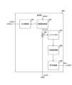
- FIG. 2 is a block diagram showing a configuration example of the analog-to-digital converter 200 in the first embodiment of the present technology.
- This analog-to-digital converter 200 includes a reference voltage generation section 210, a measurement section 250, a correction value table 261, a multiplexer 262, an analog-to-digital conversion circuit 263, and a correction section 265.
- the reference voltage generation section 210 generates a reference voltage Vref according to the control signal CTRL from the measurement section 250 and supplies it to the multiplexer 262.
- a DAC Digital to Analog Converter
- the reference voltage generation unit 210 generates a multi-step voltage that covers the entire input range of the analog-to-digital conversion circuit 263 as the reference voltage Vref. For example, if the resolution of the analog-to-digital conversion circuit 263 is n bits (n is an integer), 2 n levels of voltages obtained by dividing the input range by 2 n are sequentially generated as the reference voltage Vref.
- the correction value table 261 holds a correction value INL corr for correcting an integral non-linearity (INL) error of the analog-to-digital conversion circuit 263.
- INL integral non-linearity
- the multiplexer 262 selects either the analog input signal Ain from the tuner 120 or the reference voltage Vref according to the mode signal MODE, and supplies the selected signal to the analog-to-digital conversion circuit 263. Note that the multiplexer 262 is an example of a selection unit described in the claims.
- the mode signal MODE is a signal instructing either the calibration mode or the normal mode, and is input from outside the analog-to-digital converter 200, for example.
- the calibration mode is a mode in which the analog-to-digital converter 200 measures its own INL error and generates a correction value INL corr .
- the normal mode is a mode in which the analog-to-digital converter 200 converts the input signal Ain (analog signal) into a digital signal Dout.
- the multiplexer 262 selects the reference voltage Vref in the calibration mode and selects the input signal Ain in the normal mode.
- the analog-to-digital conversion circuit 263 converts the analog signal from the multiplexer 262 into a digital signal Dact, and supplies it to the measurement section 250 and the correction section 265.
- a single slope type ADC Analog to Digital Converter
- SARADC Sauccessive Approximation Register ADC
- the digital signal is also supplied to an access circuit (not shown) that accesses the correction value table 261.
- the access circuit reads the correction value INL corr corresponding to the digital signal from the memory and supplies it to the correction unit 250.
- the correction unit 265 corrects the digital signal Dact.
- the correction unit 265 obtains a correction value INL corr corresponding to the value of the digital signal Dact from the correction value table 261 in the normal mode. Then, the correction unit 265 corrects the digital signal Dact using the correction value INL corr , and supplies the corrected digital signal to the demodulation unit 131 as Dout.
- the measurement unit 250 measures the digital signal Dact and obtains a correction value INL corr .
- the measuring section 250 controls the reference voltage generating section 210 to sequentially generate 2 n levels of reference voltages Vref. Then, the measurement unit 250 calculates a correction value INL corr from the measured value of the digital signal Dact corresponding to the reference voltage Vref and the ideal value when there is no INL error, and stores it in the correction value table 261.
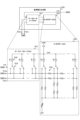
- FIG. 3 is a block diagram and a circuit diagram showing a configuration example of the reference voltage generation section 210 in the first embodiment of the present technology.
- This reference voltage generation section 210 includes, for example, a thermometer code DAC 211 and an R-2R ladder DAC 212.
- the upper bits of the control signal CTRL are input to the thermometer code DAC 211, and the lower bits are input to the R-2R ladder DAC 212.
- a plurality of current sources 213, a plurality of switches 214, and a plurality of resistance elements 215 are arranged in these DACs.
- Current source 213 supplies a constant current. It is assumed that the current value of this current source 213 can be changed by a set value of a register or the like.
- the switch 214 connects the corresponding current source 213 to either the positive output line or the negative output line, depending on the value of the corresponding bit of the control signal CTRL.
- the circuit configuration illustrated in the figure generates a positive voltage Vref_p and a negative voltage Vref_n. These differences correspond to the reference voltage Vref.
- FIG. 4 is a diagram for explaining a method for adjusting the output range of the reference voltage generation section 210 in the first embodiment of the present technology.
- the output range of the reference voltage generation section 210 can be adjusted by changing the current value of each current source 213. In order to improve the accuracy of correction, it is preferable to make the output range approximately match the input range of the analog-to-digital conversion circuit 263 by adjusting the current value. Specifically, when the control signal CTRL to the reference voltage generation unit 210 is set to "0", the value of the digital signal Dact becomes "0", and when the control signal CTRL is set to full scale, the value of the digital signal Dact becomes "0". Just adjust it so that it is full scale.
- FIG. 5 is a block diagram illustrating a configuration example of the measurement unit 250 in the first embodiment of the present technology.
- the measurement section 250 includes a DAC control section 251, an ideal value supply section 252, an adder 253, and a sign inversion section 259.
- the DAC control unit 251 generates a control signal CTRL[i] for generating a reference voltage Vref[i] corresponding to the index i from the ideal value supply unit 252, and supplies it to the reference voltage generation unit 210.
- the index i is a value assigned to each of the 2 n levels of reference voltage Vref, and is set to, for example, 0 to 2 n -1.
- the ideal value supply unit 252 supplies the ideal value D ideal .
- the ideal value supply section 252 sequentially generates an index i from 0 to 2 n -1 using a counter or the like and supplies it to the DAC control section 251 . Further, the DAC control unit 251 sequentially generates an ideal value D ideal [i] obtained by converting the corresponding reference voltage Vref[i] for each index i, and supplies the ideal value D ideal [i] to the adder 253 . For example, the same value (0 to 2 n ⁇ 1) as the index i is generated as the ideal value D ideal [i].
- index i and the corresponding ideal value D ideal [i] are not limited to the same value.
- the adder 253 subtracts the ideal value D ideal [i] from the value (measured value) of the digital signal Dact[i] corresponding to the reference voltage Vref[i], and supplies the result to the sign inverting section 259 .
- the sign inverter 259 inverts the sign of the subtraction result of the adder 253 and stores it in the correction value table 261 as a correction value INL corr [i].
- the correction value table 261 holds correction values INL corr [i] in association with index i.
- the correction value INL corr [i] is a correction value for correcting the digital signal Dact[i] corresponding to index i.
- the correction unit 265 acquires the corresponding correction value INL corr [i] from the correction value table 261, and sets the correction value INL corr [i] to the value of the digital signal Dact[i]. ] is added. Then, the correction unit 265 outputs the corrected digital signal as Dout.
- the adder 253 may subtract the ideal value D ideal [i] from the digital signal Dact[i] and supply it as the correction value INL corr [i].
- the sign inverter 259 is not necessary, and the corrector 265 only needs to subtract the correction value INL corr [i] from the digital signal Dact[i].
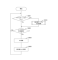
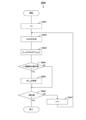
- FIG. 6 is a flowchart illustrating an example of the operation of the analog-to-digital converter 200 in the first embodiment of the present technology. This operation is started, for example, when the power is turned on.
- the analog-to-digital converter 200 determines whether the current mode is the calibration mode (step S901). If the mode is calibration mode (step S901: Yes), the analog-to-digital converter 200 starts correction value table generation processing (step S910). After the correction value table generation process (step S910) is completed, the calibration mode is switched to the normal mode, and steps S902 and subsequent steps are executed.
- step S901 determines whether an analog input signal has been input (step S902). If no input signal is input (step S902: No), the analog-to-digital converter 200 repeats step S901.
- step S902 if the input signal is input (step S902: Yes), the analog-to-digital converter 200 performs AD (Analog to Digital) conversion of the input signal to a digital signal (step S903). Then, the analog-to-digital converter 200 obtains the corresponding correction value from the correction value table 261, and corrects the digital signal using the correction value (step S905). After step S905, the analog-to-digital converter 200 repeats steps S901 and subsequent steps.
- AD Analog to Digital
- FIG. 7 is a flowchart illustrating an example of correction value table generation processing in the first embodiment of the present technology.
- the correction unit 265 in the analog-to-digital converter 200 sets the index i to an initial value (for example, "0") (step S911).
- the reference voltage generation section 210 generates the reference voltage Vref[i] under the control of the measurement section 250 (step S912).
- the measurement unit 250 calculates the error D error using the following equation (step S913).
- D error Dact [i] - D ideal [i] ...Formula 1
- the measuring unit 250 causes the correction value table 261 to hold the value obtained by inverting the sign of the error D error calculated using Equation 1 as the correction value INL corr [i] (step S914).
- the measuring unit 250 determines whether the index i is the maximum value (2 n ⁇ 1, etc.) (step S915). If the index i is not the maximum value (step S915: No), the measurement unit 250 increments the index i (step S916), and repeats steps S912 and subsequent steps. On the other hand, if the index i is the maximum value (step S915: Yes), the measurement unit 250 ends the correction value table generation process.
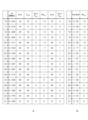
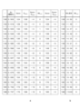
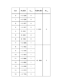
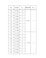
- FIG. 8 is a diagram showing correction examples and correction values corresponding to indexes 0 to 15 in the first embodiment of the present technology.
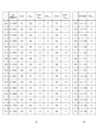
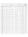
- FIG. 9 is a diagram showing correction examples and correction values corresponding to indexes 16 to 31 in the first embodiment of the present technology.
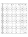
- FIG. 10 is a diagram showing correction examples and correction values corresponding to indexes 32 to 47 in the first embodiment of the present technology.
- FIG. 11 is a diagram showing correction examples and correction values corresponding to indexes 48 to 63 in the first embodiment of the present technology.
- a indicates a summary of the results of correction
- b in each indicates a correction value held in the correction value table 261.
- the resolution of the analog-to-digital converter 200 is assumed to be 6 bits. Note that the resolution is not limited to 6 bits.
- the correction value table 261 holds correction values INL corr [i] in association with index i.
- the INL component is shown for reference, but this component is not held in the correction value table 261.
- the input signal Ain of a in FIG. 8 is a signal standardized to be from "0.000" to "1.000".
- the correction unit 265 can correct the digital signal by simple calculation.
- FIG. 12 is a diagram illustrating an example of the relationship between the INL component and SINAD in the first embodiment of the present technology.
- SINAD is expressed as a ratio of Signal and Noise+Distortion, and Distortion increases in proportion to INL.
- the vertical axis indicates SINAD
- the horizontal axis indicates INL component.
- the dotted line indicates the SINAD characteristic with respect to the INL value
- the solid line indicates Noise+INL (Distortion 2 shows the SINAD characteristics for
- the INL component As illustrated in the figure, as the INL component increases, SINAD, which is an index of the performance of the analog-to-digital converter 200, deteriorates. Therefore, by suppressing the INL component, the performance of the analog-to-digital converter 200 can be improved. By correcting using the correction value table 261, the INL component can be suppressed as illustrated in the figure.
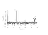
- FIG. 13 is a diagram showing an example of the frequency characteristics before correction when a sine wave signal is input in the first embodiment of the present technology.
- the horizontal axis indicates the frequency of the sine wave input signal
- the vertical axis indicates the level of the output signal before correction.
- third harmonic distortion occurs in the circled portion due to the INL component.
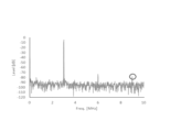
- FIG. 14 is a diagram showing an example of frequency characteristics after correction when a sine wave signal is input in the first embodiment of the present technology. Since the INL component is suppressed by the correction, the third harmonic distortion in the circled portion can be reduced and SINAD can be improved, as illustrated in the figure.
- FIGS. 13 and 14 illustrate cases in which third-order harmonic distortion is suppressed
- harmonic distortion components depend on a correction value table (correction value table 261, etc.) that reflects the characteristics of the INL, and the third-order harmonic distortion is suppressed.
- SINAD can be improved by correction for all components other than harmonic distortion components.
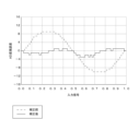
- FIG. 15 is a diagram illustrating an example of the INL component and correction value corresponding to the input signal in the first embodiment of the present technology.
- the vertical axis in the figure shows the INL component or correction value
- the horizontal axis shows the input signal normalized to a range from "0.0" to "1.0".
- the dashed line indicates the INL component
- the solid line indicates the correction value.
- a correction value having a polarity opposite to that of the INL component is generated.
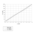
- FIG. 16 is a diagram for explaining the effect of correction in the first embodiment of the present technology.
- the horizontal axis represents an analog input signal standardized to a range from “0.0" to "1.0”
- the vertical axis represents a digital signal.
- the coarse dotted line is a straight line indicating an ideal input/output relationship
- the fine dotted line indicates the locus of the digital signal Dact before correction corresponding to the input signal.
- the solid line indicates the trajectory of the corrected digital signal Dout corresponding to the input signal.
- the difference between the ideal value and the value of the digital signal Dact may become large, resulting in an INL error.
- the value of the digital signal Dout approaches the ideal value, and the INL error can be reduced.
- FIG. 17 is a diagram illustrating an example of an AD conversion error corresponding to an input signal in the first embodiment of the present technology.
- the horizontal axis represents an analog input signal standardized to a range from “0.0" to "1.0”
- the vertical axis represents an AD conversion error.
- the dashed line indicates the AD conversion error before correction (in other words, Dact-D ideal )
- the solid line indicates the AD conversion error after correction (in other words, Dout-D ideal ).
- the error from the ideal value D ideal can be suppressed to within 1LSB (Least Significant Bit) by correction.
- the correction unit 265 corrects the digital signal using the correction values in the correction value table 261, so that the correction unit 265 corrects the digital signal using the correction value in the correction value table 261.
- the circuit scale can be reduced.
- the analog-to-digital converter 200 converts the analog signal into an n-bit code (digital signal Dout), but it may be necessary to improve the correction accuracy.
- the analog-to-digital converter 200 in this second embodiment differs from the first embodiment in that the correction accuracy is further improved by sign extension.
- FIG. 18 is a block diagram showing a configuration example of an analog-to-digital converter 200 in the second embodiment of the present technology.
- the analog-to-digital converter 200 of this second embodiment differs from the first embodiment in that it further includes a multiplier 264.
- the multiplier 264 multiplies the n-bit digital signal Dact by 2 m (m is an integer). By this multiplication, the bit width of the digital signal is sign-extended from n bits to n+m bits.
- the expanded digital signal is supplied to the correction unit 265 as a digital signal Dacte.
- correction unit 265 of the second embodiment corrects the digital signal Dacte using a correction value and outputs it as Doute.
- FIG. 19 is a block diagram illustrating a configuration example of the measurement unit 250 in the second embodiment of the present technology.
- the measuring unit 250 of this second embodiment differs from the first embodiment in that it further includes an integrator 254 and a divider 255.
- the DAC control unit 251 of the second embodiment controls the reference voltage generation unit 210 to repeat the corresponding reference voltage Vref[i] for each index i over 2 m+k (k is an integer) times. Generate.
- the adder 253 supplies 2 m+k errors D error [i] to the integrator 254 for each index i.
- the integrator 254 integrates 2 m+k errors D error [i] for each index i. This integrator 254 supplies the calculation result to a divider 255.
- the divider 255 divides the calculation result of the integrator 254 by 2k .
- the sign inverter 259 causes the correction value table 261 to hold the value obtained by inverting the sign of the division result as the correction value INL corr [i].
- the measurement unit 250 can generate a correction value for correcting the expanded digital signal Dacte.
- FIG. 20 is a flowchart illustrating an example of the operation of the analog-to-digital converter 200 in the second embodiment of the present technology.
- the operation of the analog-to-digital converter 200 of this second embodiment differs from the first embodiment in that step S904 is further executed and step S920 is executed instead of step S910.
- step S903 After AD conversion (step S903), the analog-to-digital converter 200 sign-extends the digital signal Dact (step S904), and corrects it with a correction value (step S905).
- FIG. 21 is a flowchart illustrating an example of correction value table generation processing in the second embodiment of the present technology.
- the measuring unit 250 sets the index i to the initial value (“0”) (step S921), and sets the index j and the variable Dint to the initial values (“1” and “0”) (step S922).
- Index j indicates the number of integrations.
- the reference voltage generation section 210 generates the reference voltage Vref[i] under the control of the measurement section 250 (step S923).
- the measurement unit 250 calculates the error D error using Equation 1 (step S924).
- the measuring unit 250 updates Dint with the value obtained by adding the error D error to Dint (step S925).
- the measuring unit 250 determines whether the index j is the maximum value (such as 2 m+k ) (step S926). If the index j is not the maximum value (step S926: No), the analog-to-digital converter 200 increments the index j (step S927), and repeats steps S923 and subsequent steps.
- the index j is the maximum value (such as 2 m+k ) (step S926). If the index j is not the maximum value (step S926: No), the analog-to-digital converter 200 increments the index j (step S927), and repeats steps S923 and subsequent steps.
- step S926 the measuring unit 250 divides Dint by 2 k , and sets the value obtained by inverting the sign of the result as the correction value INL corr [i] in the correction value table. 261 (step S928).
- the measuring unit 250 determines whether the index i is the maximum value (2 n+m ⁇ 2 m , etc.) (step S929). If the index i is not the maximum value (step S929: No), the measurement unit 250 adds 2 m to the index i (step S930), and repeats steps S922 and subsequent steps. On the other hand, if the index i is the maximum value (step S929: Yes), the measurement unit 250 ends the correction value table generation process.
- FIG. 22 is a diagram showing correction examples and correction values corresponding to indexes 0 to 60 in the second embodiment of the present technology.
- FIG. 23 is a diagram showing correction examples and correction values corresponding to the indices 64 to 124 in the second embodiment of the present technology.
- FIG. 24 is a diagram showing correction examples and correction values corresponding to indexes 128 to 188 in the second embodiment of the present technology.
- FIG. 25 is a diagram showing correction examples and correction values corresponding to the indexes 192 to 252 in the second embodiment of the present technology.
- a indicates a summary of the results of correction
- b in each indicates a correction value held in the correction value table 261.
- the bit width of the digital signal before expansion is 6 bits
- the bit width after expansion is 8 bits.
- the index i values obtained by multiplying each of 0 to 63 by 2 2 and expanding are used.
- an ideal value obtained by expanding the ideal value D ideal is defined as D ideal .
- the measurement unit 250 since the measurement unit 250 generates correction values from the digital signal Dact before expansion using Equations 1 and 2, the number of correction values is different from that in the first embodiment, as illustrated in FIGS. 22 to 25. is the same as (2 6 , etc.). Thereby, an increase in the size of the correction value table 261 can be suppressed.
- FIG. 26 is a diagram for explaining the effect of correction in the second embodiment of the present technology.
- the horizontal axis represents an analog input signal standardized to a range from "0.0" to "1.0”
- the vertical axis represents a digital signal.
- the coarse dotted line is a straight line indicating an ideal input/output relationship
- the fine dotted line indicates the locus of the uncorrected digital signal Dacte corresponding to the input signal.
- the solid line indicates the trajectory of the corrected digital signal Doute corresponding to the input signal.
- the correction accuracy is improved by sign extension, and the INL error can be further reduced.
- FIG. 27 is a diagram illustrating an example of an AD conversion error corresponding to an input signal in the second embodiment of the present technology.
- the horizontal axis represents an analog input signal standardized to a range from "0.0" to "1.0”
- the vertical axis represents an AD conversion error.
- the dashed line indicates the AD conversion error before correction (in other words, Dacte-D ideale )
- the solid line indicates the AD conversion error after correction (in other words, Doute-D ideale ).
- the correction accuracy is improved by sign extension, and the error from the ideal value D ideal can be further suppressed.
- the digital signal is sign-extended, so that the correction accuracy can be further improved.
- the measuring unit 250 generates a correction value for each value of the digital signal, but in this configuration, the size of the correction value table 261 increases as the resolution increases. .
- the analog-to-digital converter 200 in the third embodiment differs from the first embodiment in that the size of the correction value table 261 is reduced.
- FIG. 28 is a block diagram illustrating a configuration example of the measurement unit 250 in the third embodiment of the present technology.
- the measurement section 250 of this third embodiment differs from the first embodiment in that it further includes a buffer memory 257 and a representative value acquisition section 258.
- the adder 253 causes the buffer memory 257 to hold the difference (ie, error D error ) between the ideal value D ideal and the digital signal Dact.
- the value of the digital signal Dact is divided into multiple ranges. For example, if the value of the digital signal Dact is 0 to 63, those 64 codes are divided into 8 ranges of 8 codes each.
- the buffer memory 257 holds at least eight errors .
- the representative value acquisition unit 258 reads out the error D error within the divided range from the buffer memory 257 for each divided range, and acquires their representative values (such as the most frequent value).
- the sign inverter 259 causes the correction value table 261 to hold a value obtained by inverting the sign of the representative value for each range as a correction value for that range.
- FIG. 29 is a flowchart illustrating an example of correction value table generation processing in the third embodiment of the present technology.
- the measuring unit 250 sets the index i to an initial value (“0”) (step S941). Then, the reference voltage generation unit 210 generates the reference voltage Vref[i] (step S942).
- the measurement unit 250 calculates the error D error [i] using the following equation and stores it in the buffer memory 257 (step S943).
- D error [i] Dact [i] - D ideal [i] ...Formula 3
- the measuring unit 250 determines whether the index i is the maximum value (such as 7 or 15) within the divided range (step S944). If i is the maximum value within the range (step S944: Yes), the measurement unit 250 acquires the representative value within the range, and stores the value with its sign inverted as the correction value INL rep in the correction value table 261. (step S945).
- step S944 determines whether the index i is the maximum value of the entire range (such as 2 n ⁇ 1). (Step S946).
- step S946 If the index i is not the maximum value (step S946: No), the measurement unit 250 increments the index i (step S947) and repeats steps S942 and subsequent steps. On the other hand, if the index i is the maximum value (step S946: Yes), the measurement unit 250 ends the correction value table generation process.
- FIG. 30 is a diagram showing correction values corresponding to digital signals from 0 to 15 in the third embodiment of the present technology.
- FIG. 31 is a diagram showing correction values corresponding to digital signals 16 to 31 in the third embodiment of the present technology.
- FIG. 32 is a diagram showing correction values corresponding to digital signals 32 to 47 in the third embodiment of the present technology.
- FIG. 33 is a diagram showing correction values corresponding to digital signals 48 to 63 in the third embodiment of the present technology.
- the correction values illustrated in FIGS. 30 to 33 are held in the correction value table 261.
- the values of the digital signal Dact are 0 to 63, which are divided into eight ranges.
- the error D error is calculated using Equation 3.
- a value obtained by inverting the sign of these representative values is held in the correction value table 261 as a correction value INL rep corresponding to the range.
- the correction value INL rep of "0" is held in association with the range of the digital signal Dact from 0 to 7.
- the size of the correction value table 261 can be adjusted by holding in the correction value table 261 a value obtained by inverting the sign of the representative value of the error within that range as a correction value. can be reduced.
- FIG. 34 is a diagram showing an example of correction corresponding to indexes 0 to 15 in the third embodiment of the present technology.
- FIG. 35 is a diagram showing an example of correction corresponding to indexes 16 to 31 in the third embodiment of the present technology.
- FIG. 36 is a diagram showing an example of correction corresponding to indexes 32 to 47 in the third embodiment of the present technology.
- FIG. 37 is a diagram showing an example of correction corresponding to indexes 48 to 63 in the third embodiment of the present technology.
- FIG. 38 is a diagram for explaining the effect of correction in the third embodiment of the present technology.
- the horizontal axis indicates the input signal
- the vertical axis indicates the digital signal.
- the coarse dotted line is a straight line indicating an ideal input/output relationship
- the fine dotted line indicates the locus of the digital signal Dact before correction corresponding to the input signal.
- the solid line indicates the trajectory of the corrected digital signal Dout corresponding to the input signal.
- the INL error can be reduced by correction.
- FIG. 39 is a diagram showing an example of INL components before and after correction in the third embodiment of the present technology.
- the vertical axis shows the INL component
- the horizontal axis shows the input signal.
- the dotted line indicates the INL component before correction
- the solid line indicates the INL component after correction. As illustrated in the figure, the INL component is reduced by the correction.
- FIG. 40 is a diagram illustrating an example of an AD conversion error corresponding to an input signal in the third embodiment of the present technology.
- the horizontal axis in the figure shows the input signal, and the vertical axis shows the AD conversion error.
- the dashed line indicates the AD conversion error before correction, and the solid line indicates the AD conversion error after correction.
- the error from the ideal value D ideal can be suppressed by correction.
- the correction value table 261 holds, for each range of the digital signal, a value obtained by inverting the sign of the representative error value within that range as a correction value. Therefore, the size of the table can be reduced compared to the first embodiment.
- An analog-to-digital conversion circuit that converts analog signals to digital signals; a correction value table that stores correction values for correcting nonlinearity errors of the analog-to-digital conversion circuit in association with values of the digital signal;
- An analog-to-digital converter comprising: a correction section that corrects the digital signal using the correction value.
- a reference voltage generation unit that generates a predetermined reference voltage; a selection unit that selects one of the reference voltage and the input analog input signal and supplies the selected one to the analog-to-digital conversion circuit;
- the analog-to-digital converter according to (1) further comprising a measuring section that calculates the correction value from a measured value of the digital signal corresponding to the reference voltage and a predetermined ideal value.
- the analog-to-digital converter according to (2) wherein the output range of the reference voltage generation section substantially matches the input range of the analog-to-digital conversion circuit.
- the measuring unit calculates the difference between the measured value and the ideal value as the correction value, The analog-to-digital converter according to (2) or (3), wherein the correction value table holds the correction value for each value of the digital signal.
- the value of the digital signal is divided into a predetermined number of ranges; The measurement unit determines, for each range, a representative value of the difference between the measured value and the ideal value within the range as the correction value, The analog-to-digital converter according to (2) or (3), wherein the correction value table holds the correction values for each range.
- (6) further comprising a multiplier that sign-extends the digital signal by multiplication and supplies it to the correction unit;
- the resolution of the analog-to-digital conversion circuit is n bits, where n is an integer;
- the multiplier multiplies the digital signal by 2 m , where m is an integer,
- the number of times the difference is integrated is 2 (k+m) , where k is an integer,
- an analog-to-digital conversion circuit that converts analog signals to digital signals; a correction value table that stores correction values for correcting nonlinearity errors of the analog-to-digital conversion circuit in association with values of the digital signal; a correction unit that corrects the digital signal using the correction value;
- An electronic device comprising: a signal processing unit that performs predetermined processing on the corrected digital signal.
- an analog-to-digital conversion procedure for converting an analog signal into a digital signal; a correction step of correcting the digital signal using the correction value obtained from a correction value table that stores correction values for correcting non-linearity errors of the analog-to-digital conversion circuit in association with the values of the digital signal;
- a method for controlling an analog-to-digital converter comprising:
Landscapes
- Engineering & Computer Science (AREA)
- Theoretical Computer Science (AREA)
- Analogue/Digital Conversion (AREA)
Abstract
Description
1.第1の実施の形態(補正値テーブルの補正値を用いて補正する例)
2.第2の実施の形態(符号拡張し、補正値テーブルの補正値を用いて補正する例)
3.第3の実施の形態(代表値を補正値として補正値テーブルに保持し、補正値を用いて補正する例)
[電子装置の構成例]
図1は、本技術の第1の実施の形態における受信装置100の一構成例を示すブロック図である。この受信装置100は、地上デジタル放送信号などの無線信号を受信するための装置であり、アンテナ110、チューナー120、復調処理部130、および、映像音声処理部140を備える。また、復調処理部130は、アナログデジタル変換器200および復調部131を備える。映像音声処理部140は、多重分離部141およびデコーダ142を備える。
図2は、本技術の第1の実施の形態におけるアナログデジタル変換器200の一構成例を示すブロック図である。このアナログデジタル変換器200は、基準電圧生成部210、測定部250、補正値テーブル261、マルチプレクサ262、アナログデジタル変換回路263および補正部265を備える。
図3は、本技術の第1の実施の形態における基準電圧生成部210の一構成例を示すブロック図および回路図である。この基準電圧生成部210は、例えば、サーモメータコードDAC211およびR-2RラダーDAC212を備える。例えば、制御信号CTRLの上位ビットがサーモメータコードDAC211に入力され、下位ビットがR-2RラダーDAC212に入力される。
図5は、本技術の第1の実施の形態における測定部250の一構成例を示すブロック図である。この測定部250は、DAC制御部251、理想値供給部252、加算器253および符号反転部259を備える。
図6は、本技術の第1の実施の形態におけるアナログデジタル変換器200の動作の一例を示すフローチャートである。この動作は、例えば、電源が投入されたときに開始される。
Derror=Dact[i]-Dideal[i] ・・・式1
に対するSINAD特性を示す。
上述の第1の実施の形態では、アナログデジタル変換器200は、アナログ信号をnビットのコード(デジタル信号Dоut)に変換していたが、補正精度の向上が必要な場合がある。この第2の実施の形態におけるアナログデジタル変換器200は、符号拡張により補正精度をさらに向上させた点において第1の実施の形態と異なる。

上述の第1の実施の形態では、測定部250は、デジタル信号の値ごとに補正値を生成していたが、この構成では、分解能が高くなるほど、補正値テーブル261のサイズが増大してしまう。この第3の実施の形態におけるアナログデジタル変換器200は、補正値テーブル261のサイズを削減した点において第1の実施の形態と異なる。
Derror[i]=Dact[i]-Dideal[i] ・・・式3
(1)アナログ信号をデジタル信号に変換するアナログデジタル変換回路と、
前記アナログデジタル変換回路の非直線性誤差を補正するための補正値を前記デジタル信号の値に対応付けて保持する補正値テーブルと、
前記補正値を用いて前記デジタル信号を補正する補正部と
を具備するアナログデジタル変換器。
(2)所定の基準電圧を生成する基準電圧生成部と、
前記基準電圧と入力されたアナログの入力信号との一方を選択して前記アナログデジタル変換回路に供給する選択部と、
前記基準電圧に対応する前記デジタル信号の測定値と所定の理想値とから前記補正値を求める測定部と
をさらに具備する前記(1)記載のアナログデジタル変換器。
(3)前記基準電圧生成部の出力レンジは、前記アナログデジタル変換回路の入力レンジと略一致する
前記(2)記載のアナログデジタル変換器。
(4)前記測定部は、前記測定値と前記理想値との差分を前記補正値として求め、
前記補正値テーブルは、前記デジタル信号の値ごとに前記補正値を保持する
前記(2)または(3)に記載のアナログデジタル変換器。
(5)前記デジタル信号の値は、所定数の範囲に分割され、
前記測定部は、前記範囲ごとに当該範囲内の前記測定値および前記理想値の差分の代表値を前記補正値として求め、
前記補正値テーブルは、前記範囲ごとに前記補正値を保持する
前記(2)または(3)に記載のアナログデジタル変換器。
(6)前記デジタル信号を乗算により符号拡張して前記補正部に供給する乗算器をさらに具備し、
前記測定部は、前記測定値と前記理想値との差分の積算値を所定の除数により除算した値を前記補正値として演算する
を備える前記(2)または(3)に記載のアナログデジタル変換器。
(7)前記アナログデジタル変換回路の分解能は、nを整数としてnビットであり、
前記乗算器は、mを整数として2mを前記デジタル信号に乗算し、
前記差分の積算回数は、kを整数として2(k+m)であり、
前記除数は、2kである
前記(6)記載のアナログデジタル変換器。
(8)アナログ信号をデジタル信号に変換するアナログデジタル変換回路と、
前記アナログデジタル変換回路の非直線性誤差を補正するための補正値を前記デジタル信号の値に対応付けて保持する補正値テーブルと、
前記補正値を用いて前記デジタル信号を補正する補正部と、
前記補正されたデジタル信号に対して所定の処理を行う信号処理部と
を具備する電子装置。
(9)アナログ信号をデジタル信号に変換するアナログデジタル変換手順と、
前記アナログデジタル変換回路の非直線性誤差を補正するための補正値を前記デジタル信号の値に対応付けて保持する補正値テーブルから取得した前記補正値を用いて前記デジタル信号を補正する補正手順と
を具備するアナログデジタル変換器の制御方法。
110 アンテナ
120 チューナー
130 復調処理部
131 復調部
140 映像音声処理部
141 多重分離部
142 デコーダ
150 ディスプレイ
200 アナログデジタル変換器
210 基準電圧生成部
211 サーモメータコードDAC
212 R-2RラダーDAC
213 電流源
214 スイッチ
215 抵抗素子
250 測定部
251 DAC制御部
252 理想値供給部
253 加算器
254 積算器
255 除算器
257 バッファメモリ
258 代表値取得部
259 符号反転部
261 補正値テーブル
262 マルチプレクサ
263 アナログデジタル変換回路
264 乗算器
265 補正部
Claims (9)
- アナログ信号をデジタル信号に変換するアナログデジタル変換回路と、
前記アナログデジタル変換回路の非直線性誤差を補正するための補正値を前記デジタル信号の値に対応付けて保持する補正値テーブルと、
前記補正値を用いて前記デジタル信号を補正する補正部と
を具備するアナログデジタル変換器。 - 所定の基準電圧を生成する基準電圧生成部と、
前記基準電圧と入力されたアナログの入力信号との一方を選択して前記アナログデジタル変換回路に供給する選択部と、
前記基準電圧に対応する前記デジタル信号の測定値と所定の理想値とから前記補正値を求める測定部と
をさらに具備する請求項1記載のアナログデジタル変換器。 - 前記基準電圧生成部の出力レンジは、前記アナログデジタル変換回路の入力レンジと略一致する
請求項2記載のアナログデジタル変換器。 - 前記測定部は、前記測定値と前記理想値との差分を前記補正値として求め、
前記補正値テーブルは、前記デジタル信号の値ごとに前記補正値を保持する
請求項2記載のアナログデジタル変換器。 - 前記デジタル信号の値は、所定数の範囲に分割され、
前記測定部は、前記範囲ごとに当該範囲内の前記測定値および前記理想値の差分の代表値を前記補正値として求め、
前記補正値テーブルは、前記範囲ごとに前記補正値を保持する
請求項2記載のアナログデジタル変換器。 - 前記デジタル信号を乗算により符号拡張して前記補正部に供給する乗算器をさらに具備し、
前記測定部は、前記測定値と前記理想値との差分の積算値を所定の除数により除算した値を前記補正値として演算する
を備える請求項2記載のアナログデジタル変換器。 - 前記アナログデジタル変換回路の分解能は、nを整数としてnビットであり、
前記乗算器は、mを整数として2mを前記デジタル信号に乗算し、
前記差分の積算回数は、kを整数として2(k+m)であり、
前記除数は、2kである
請求項6記載のアナログデジタル変換器。 - アナログ信号をデジタル信号に変換するアナログデジタル変換回路と、
前記アナログデジタル変換回路の非直線性誤差を補正するための補正値を前記デジタル信号の値に対応付けて保持する補正値テーブルと、
前記補正値を用いて前記デジタル信号を補正する補正部と、
前記補正されたデジタル信号に対して所定の処理を行う信号処理部と
を具備する電子装置。 - アナログ信号をデジタル信号に変換するアナログデジタル変換手順と、
前記アナログデジタル変換回路の非直線性誤差を補正するための補正値を前記デジタル信号の値に対応付けて保持する補正値テーブルから取得した前記補正値を用いて前記デジタル信号を補正する補正手順と
を具備するアナログデジタル変換器の制御方法。
Priority Applications (1)
| Application Number | Priority Date | Filing Date | Title |
|---|---|---|---|
| JP2024520274A JPWO2023218756A1 (ja) | 2022-05-11 | 2023-03-16 |
Applications Claiming Priority (2)
| Application Number | Priority Date | Filing Date | Title |
|---|---|---|---|
| JP2022078112 | 2022-05-11 | ||
| JP2022-078112 | 2022-05-11 |
Publications (1)
| Publication Number | Publication Date |
|---|---|
| WO2023218756A1 true WO2023218756A1 (ja) | 2023-11-16 |
Family
ID=88729993
Family Applications (1)
| Application Number | Title | Priority Date | Filing Date |
|---|---|---|---|
| PCT/JP2023/010334 Ceased WO2023218756A1 (ja) | 2022-05-11 | 2023-03-16 | アナログデジタル変換器、電子装置、および、アナログデジタル変換器の制御方法 |
Country Status (3)
| Country | Link |
|---|---|
| JP (1) | JPWO2023218756A1 (ja) |
| TW (1) | TW202349881A (ja) |
| WO (1) | WO2023218756A1 (ja) |
Citations (3)
| Publication number | Priority date | Publication date | Assignee | Title |
|---|---|---|---|---|
| JP2007521743A (ja) * | 2003-06-27 | 2007-08-02 | オプティクロン・インコーポレーテッド | アナログデジタル変換器 |
| WO2009047865A1 (ja) * | 2007-10-12 | 2009-04-16 | Fujitsu Limited | 受信回路、受信回路のadコンバータの変換テーブル作成方法、および信号伝送システム |
| JP2016213531A (ja) * | 2015-04-28 | 2016-12-15 | 国立大学法人金沢大学 | Ad変換器およびad変換方法 |
-
2023
- 2023-03-16 WO PCT/JP2023/010334 patent/WO2023218756A1/ja not_active Ceased
- 2023-03-16 JP JP2024520274A patent/JPWO2023218756A1/ja active Pending
- 2023-04-21 TW TW112114980A patent/TW202349881A/zh unknown
Patent Citations (3)
| Publication number | Priority date | Publication date | Assignee | Title |
|---|---|---|---|---|
| JP2007521743A (ja) * | 2003-06-27 | 2007-08-02 | オプティクロン・インコーポレーテッド | アナログデジタル変換器 |
| WO2009047865A1 (ja) * | 2007-10-12 | 2009-04-16 | Fujitsu Limited | 受信回路、受信回路のadコンバータの変換テーブル作成方法、および信号伝送システム |
| JP2016213531A (ja) * | 2015-04-28 | 2016-12-15 | 国立大学法人金沢大学 | Ad変換器およびad変換方法 |
Also Published As
| Publication number | Publication date |
|---|---|
| JPWO2023218756A1 (ja) | 2023-11-16 |
| TW202349881A (zh) | 2023-12-16 |
Similar Documents
| Publication | Publication Date | Title |
|---|---|---|
| CN101595643B (zh) | 数字模拟转换器和用于校准该数字模拟转换器的方法 | |
| US6486807B2 (en) | A/D converter calibration | |
| CN102859882B (zh) | 具有积分非线性度校正的逐次逼近寄存器模拟/数字转换器 | |
| US6958722B1 (en) | SAR ADC providing digital codes with high accuracy and high throughput performance | |
| US7142138B2 (en) | Multi-step analog/digital converter and on-line calibration method thereof | |
| US8451151B2 (en) | Successive approximation analog to digital converter with capacitor mismatch calibration and method thereof | |
| JPH06104754A (ja) | 梯子型抵抗をトリミングするための既埋設修正データメモリを備えた多段アナログデジタル変換器 | |
| US7830287B1 (en) | Analog to digital converter having digital correction logic that utilizes a dither signal to correct a digital code | |
| CN104518797A (zh) | 一种用于高精度模数转换器中的抖动电路 | |
| CN103873784B (zh) | 图像拾取装置、图像拾取系统及用于驱动该装置的方法 | |
| TWI442710B (zh) | 訊號處理系統及其自我校準數位類比轉換方法 | |
| TWI645680B (zh) | 類比至數位轉換裝置及其類比至數位轉換器校正方法 | |
| US20150200681A1 (en) | Segmented Digital-To-Analog Converter With Overlapping Segments | |
| TWI632778B (zh) | 數位類比轉換器及其執行方法 | |
| JP2010093683A (ja) | デジタルアナログ変換回路とその出力データの補正方法 | |
| CN109600139B (zh) | 模拟至数字转换装置及其模拟至数字转换器校正方法 | |
| CN118740150A (zh) | 可自动调校满刻度电压的逐次逼近模拟数字转换器及方法 | |
| WO2010137168A1 (ja) | アナログユニット | |
| TW202349881A (zh) | 類比數位轉換器、電子裝置、及類比數位轉換器之控制方法 | |
| WO2011099367A1 (ja) | A/d変換装置及びa/d変換補正方法 | |
| JP4588278B2 (ja) | アナログ−デジタル変換器 | |
| CN112311395B (zh) | 电荷型sar adc的校准方法 | |
| JP2013131838A (ja) | D/aコンバータシステムおよびそれを用いた試験装置 | |
| JP6706305B2 (ja) | アナログ信号発生装置 | |
| JPS6161577B2 (ja) |
Legal Events
| Date | Code | Title | Description |
|---|---|---|---|
| 121 | Ep: the epo has been informed by wipo that ep was designated in this application |
Ref document number: 23803239 Country of ref document: EP Kind code of ref document: A1 |
|
| ENP | Entry into the national phase |
Ref document number: 2024520274 Country of ref document: JP Kind code of ref document: A |
|
| WWE | Wipo information: entry into national phase |
Ref document number: 18862302 Country of ref document: US |
|
| NENP | Non-entry into the national phase |
Ref country code: DE |
|
| 122 | Ep: pct application non-entry in european phase |
Ref document number: 23803239 Country of ref document: EP Kind code of ref document: A1 |