WO2023218525A1 - 表示パネルの制御装置、表示装置及び表示パネルの制御方法 - Google Patents
表示パネルの制御装置、表示装置及び表示パネルの制御方法 Download PDFInfo
- Publication number
- WO2023218525A1 WO2023218525A1 PCT/JP2022/019802 JP2022019802W WO2023218525A1 WO 2023218525 A1 WO2023218525 A1 WO 2023218525A1 JP 2022019802 W JP2022019802 W JP 2022019802W WO 2023218525 A1 WO2023218525 A1 WO 2023218525A1
- Authority
- WO
- WIPO (PCT)
- Prior art keywords
- self
- emissive
- display
- pixel
- amount
- Prior art date
- Legal status (The legal status is an assumption and is not a legal conclusion. Google has not performed a legal analysis and makes no representation as to the accuracy of the status listed.)
- Ceased
Links
Images








Classifications
-
- G—PHYSICS
- G09—EDUCATION; CRYPTOGRAPHY; DISPLAY; ADVERTISING; SEALS
- G09G—ARRANGEMENTS OR CIRCUITS FOR CONTROL OF INDICATING DEVICES USING STATIC MEANS TO PRESENT VARIABLE INFORMATION
- G09G3/00—Control arrangements or circuits, of interest only in connection with visual indicators other than cathode-ray tubes
- G09G3/20—Control arrangements or circuits, of interest only in connection with visual indicators other than cathode-ray tubes for presentation of an assembly of a number of characters, e.g. a page, by composing the assembly by combination of individual elements arranged in a matrix no fixed position being assigned to or needed to be assigned to the individual characters or partial characters
- G09G3/22—Control arrangements or circuits, of interest only in connection with visual indicators other than cathode-ray tubes for presentation of an assembly of a number of characters, e.g. a page, by composing the assembly by combination of individual elements arranged in a matrix no fixed position being assigned to or needed to be assigned to the individual characters or partial characters using controlled light sources
- G09G3/30—Control arrangements or circuits, of interest only in connection with visual indicators other than cathode-ray tubes for presentation of an assembly of a number of characters, e.g. a page, by composing the assembly by combination of individual elements arranged in a matrix no fixed position being assigned to or needed to be assigned to the individual characters or partial characters using controlled light sources using electroluminescent panels
- G09G3/32—Control arrangements or circuits, of interest only in connection with visual indicators other than cathode-ray tubes for presentation of an assembly of a number of characters, e.g. a page, by composing the assembly by combination of individual elements arranged in a matrix no fixed position being assigned to or needed to be assigned to the individual characters or partial characters using controlled light sources using electroluminescent panels semiconductive, e.g. using light-emitting diodes [LED]
- G09G3/3208—Control arrangements or circuits, of interest only in connection with visual indicators other than cathode-ray tubes for presentation of an assembly of a number of characters, e.g. a page, by composing the assembly by combination of individual elements arranged in a matrix no fixed position being assigned to or needed to be assigned to the individual characters or partial characters using controlled light sources using electroluminescent panels semiconductive, e.g. using light-emitting diodes [LED] organic, e.g. using organic light-emitting diodes [OLED]
- G09G3/3225—Control arrangements or circuits, of interest only in connection with visual indicators other than cathode-ray tubes for presentation of an assembly of a number of characters, e.g. a page, by composing the assembly by combination of individual elements arranged in a matrix no fixed position being assigned to or needed to be assigned to the individual characters or partial characters using controlled light sources using electroluminescent panels semiconductive, e.g. using light-emitting diodes [LED] organic, e.g. using organic light-emitting diodes [OLED] using an active matrix
- G09G3/3233—Control arrangements or circuits, of interest only in connection with visual indicators other than cathode-ray tubes for presentation of an assembly of a number of characters, e.g. a page, by composing the assembly by combination of individual elements arranged in a matrix no fixed position being assigned to or needed to be assigned to the individual characters or partial characters using controlled light sources using electroluminescent panels semiconductive, e.g. using light-emitting diodes [LED] organic, e.g. using organic light-emitting diodes [OLED] using an active matrix with pixel circuitry controlling the current through the light-emitting element
-
- G—PHYSICS
- G09—EDUCATION; CRYPTOGRAPHY; DISPLAY; ADVERTISING; SEALS
- G09G—ARRANGEMENTS OR CIRCUITS FOR CONTROL OF INDICATING DEVICES USING STATIC MEANS TO PRESENT VARIABLE INFORMATION
- G09G3/00—Control arrangements or circuits, of interest only in connection with visual indicators other than cathode-ray tubes
- G09G3/20—Control arrangements or circuits, of interest only in connection with visual indicators other than cathode-ray tubes for presentation of an assembly of a number of characters, e.g. a page, by composing the assembly by combination of individual elements arranged in a matrix no fixed position being assigned to or needed to be assigned to the individual characters or partial characters
-
- G—PHYSICS
- G09—EDUCATION; CRYPTOGRAPHY; DISPLAY; ADVERTISING; SEALS
- G09G—ARRANGEMENTS OR CIRCUITS FOR CONTROL OF INDICATING DEVICES USING STATIC MEANS TO PRESENT VARIABLE INFORMATION
- G09G3/00—Control arrangements or circuits, of interest only in connection with visual indicators other than cathode-ray tubes
- G09G3/20—Control arrangements or circuits, of interest only in connection with visual indicators other than cathode-ray tubes for presentation of an assembly of a number of characters, e.g. a page, by composing the assembly by combination of individual elements arranged in a matrix no fixed position being assigned to or needed to be assigned to the individual characters or partial characters
- G09G3/22—Control arrangements or circuits, of interest only in connection with visual indicators other than cathode-ray tubes for presentation of an assembly of a number of characters, e.g. a page, by composing the assembly by combination of individual elements arranged in a matrix no fixed position being assigned to or needed to be assigned to the individual characters or partial characters using controlled light sources
- G09G3/30—Control arrangements or circuits, of interest only in connection with visual indicators other than cathode-ray tubes for presentation of an assembly of a number of characters, e.g. a page, by composing the assembly by combination of individual elements arranged in a matrix no fixed position being assigned to or needed to be assigned to the individual characters or partial characters using controlled light sources using electroluminescent panels
- G09G3/32—Control arrangements or circuits, of interest only in connection with visual indicators other than cathode-ray tubes for presentation of an assembly of a number of characters, e.g. a page, by composing the assembly by combination of individual elements arranged in a matrix no fixed position being assigned to or needed to be assigned to the individual characters or partial characters using controlled light sources using electroluminescent panels semiconductive, e.g. using light-emitting diodes [LED]
-
- G—PHYSICS
- G09—EDUCATION; CRYPTOGRAPHY; DISPLAY; ADVERTISING; SEALS
- G09G—ARRANGEMENTS OR CIRCUITS FOR CONTROL OF INDICATING DEVICES USING STATIC MEANS TO PRESENT VARIABLE INFORMATION
- G09G2320/00—Control of display operating conditions
- G09G2320/02—Improving the quality of display appearance
- G09G2320/0233—Improving the luminance or brightness uniformity across the screen
-
- G—PHYSICS
- G09—EDUCATION; CRYPTOGRAPHY; DISPLAY; ADVERTISING; SEALS
- G09G—ARRANGEMENTS OR CIRCUITS FOR CONTROL OF INDICATING DEVICES USING STATIC MEANS TO PRESENT VARIABLE INFORMATION
- G09G2320/00—Control of display operating conditions
- G09G2320/02—Improving the quality of display appearance
- G09G2320/0242—Compensation of deficiencies in the appearance of colours
-
- G—PHYSICS
- G09—EDUCATION; CRYPTOGRAPHY; DISPLAY; ADVERTISING; SEALS
- G09G—ARRANGEMENTS OR CIRCUITS FOR CONTROL OF INDICATING DEVICES USING STATIC MEANS TO PRESENT VARIABLE INFORMATION
- G09G2320/00—Control of display operating conditions
- G09G2320/04—Maintaining the quality of display appearance
- G09G2320/041—Temperature compensation
-
- G—PHYSICS
- G09—EDUCATION; CRYPTOGRAPHY; DISPLAY; ADVERTISING; SEALS
- G09G—ARRANGEMENTS OR CIRCUITS FOR CONTROL OF INDICATING DEVICES USING STATIC MEANS TO PRESENT VARIABLE INFORMATION
- G09G2320/00—Control of display operating conditions
- G09G2320/04—Maintaining the quality of display appearance
- G09G2320/043—Preventing or counteracting the effects of ageing
- G09G2320/045—Compensation of drifts in the characteristics of light emitting or modulating elements
Definitions
- the present disclosure relates to a display panel control device, a display device, and a display panel control method.
- display devices including self-emissive elements in self-emissive pixels have been actively developed.
- display devices whose self-emitting elements are, for example, QLEDs (Quantum dot Light Emitting Diodes) or OLEDs (Organic Light Emitting Diodes), have lower power consumption, are thinner, and have higher image quality. It is attracting a lot of attention because of its potential for achieving transformation.
- Patent Document 1 the amount of light emitted from a partial area including a plurality of self-emitting pixels is accumulated, a correction value is determined based on this cumulative amount of light emission and a reference value, and a correction value is set between adjacent partial areas. It is described that the correction value is modified according to the position within the partial area so that the correction value changes continuously.
- the inventors of the present disclosure have conducted an aging test (a test in which a burned area including a plurality of self-emissive pixels continues to be displayed for a predetermined period of time) on a display device including a self-emissive element in a self-emissive pixel.
- a mixed color for example, white, cyan (C), magenta (M), or yellow ( It has been found that the self-emissive element included in the self-emissive pixel that emits part of the mixed color in the area printed while displaying Y)) may have a larger amount of change over time (amount of deterioration).
- the inventors of the present disclosure have discovered that a large change (deterioration) occurs over time in a self-emissive element included in a self-emissive pixel that emits a part of the mixed color around the area where the mixed color is printed while displaying the mixed color. (For example, it has been found that there are cases in which a change (deterioration) over time such as bleeding occurs over more than 10 surrounding pixels).
- Patent Document 1 The method described in Patent Document 1 is based on the change over time of a self-emissive element included in a self-emissive pixel that emits a part of the mixed color in an area that is printed while displaying the mixed color discovered by the inventors of the present disclosure.
- the amount of deterioration is large, or there is also a large change (deterioration) over time in a self-emissive element included in a self-emissive pixel that emits a part of the mixed color around the area where the mixed color is printed while displaying the mixed color. Since this phenomenon is not taken into account, there is a problem in that it is not possible to perform correction that accurately reflects changes over time (deterioration) due to the influence of adjacent pixels.
- One aspect of the present disclosure has been made in view of the above problems, and provides a display panel control device that can perform correction that accurately reflects the level of change (deterioration) over time due to the influence of adjacent pixels, and a display panel control device.
- the purpose is to provide a control method.
- a display panel control device including a plurality of first self-emissive pixels that output a first color light and a plurality of second self-emissive pixels that output a second color light different from the first color light,
- Each of the plurality of first self-emissive pixels is arranged within a predetermined range with respect to the corresponding second self-emissive pixel of the plurality of second self-emissive pixels, a second self-emissive pixel corresponding to the first self-emissive pixel, calculated based on a display amount of the first self-emissive pixel arranged within the predetermined range with respect to the second self-emissive pixel; an accumulation unit that accumulates an influence amount indicating the influence of the display; a compensation processing unit that generates a corrected video signal by compensating for the temporal change of each of the second self-emissive pixels based on the influence amount regarding each of the plurality of second self-emissive pixels with respect to the
- the display panel control method of the present disclosure includes the following steps: A method for controlling a display panel including a plurality of first self-emissive pixels that output a first color light and a plurality of second self-emissive pixels that output a second color light different from the first color light, the method comprising: Each of the plurality of first self-emissive pixels is arranged within a predetermined range with respect to the corresponding second self-emissive pixel of the plurality of second self-emissive pixels, a second self-emissive pixel corresponding to the first self-emissive pixel, calculated based on a display amount of the first self-emissive pixel arranged within the predetermined range with respect to the second self-emissive pixel; an accumulation step of accumulating an influence amount indicating the influence of the display; a compensation processing step of generating a corrected video signal by compensating for the temporal change of each of the second self-emissive pixels based on the influence amount regarding each of the plurality of
- control device of the present disclosure has the following features: A control device for a display panel including a first self-emissive pixel that outputs a first color light and a second self-emissive pixel that outputs a second color light different from the first color light, In a first area including a predetermined number of the first self-emissive pixels and the second self-emissive pixels on the display panel, the first self-emissive pixels are set to the minimum gradation value and the second self-emissive pixels are In addition to displaying pixels at the maximum gradation value for a predetermined time, In a second area different from the first area including the predetermined number of the first self-emissive pixels and the second self-emissive pixels on the display panel, the first self-emissive pixels and the second self-emissive pixels After displaying each of the self-emitting pixels at the maximum gradation value for the predetermined time, When each of the second self-emissive pixels included in the first area and the second self-emissive pixels included in the first
- One aspect of the present disclosure can provide a display panel control device and a display panel control method that can perform correction that accurately reflects the level of change over time (deterioration) due to the influence of adjacent pixels.
- FIG. 1 is a diagram illustrating a schematic configuration of a display panel and a control device for the display panel included in the display device of Embodiment 1.
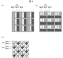
- FIG. (a), (b), and (c) are diagrams showing examples of arrangement of self-luminous pixels in a display panel included in the display device of Embodiment 1.
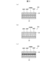
- (a) is a sectional view showing a schematic configuration of a red light-emitting element included in a red self-luminous pixel of a display panel included in the display device of Embodiment 1;
- 2 is a sectional view showing a schematic configuration of a green light-emitting element included in a green self-emission pixel of a display panel included in the device;
- FIG. 2 is a cross-sectional view showing a schematic configuration of a blue light emitting element included in a light emitting pixel.
- 4 is a diagram showing the relationship between the input gradation value and the normalized output current value in each color light emitting element shown in FIG. 3.
- FIG. 4 is a diagram showing a tendency for brightness to decrease as the amount of accumulated current of each color light emitting element shown in FIG. 3 increases.
- FIG. FIG. 3 is a diagram showing an example of a burn-in display pattern. After the R255 burn-in area shown in FIG. 6 is displayed for a predetermined time and the W255 shown in FIG. FIG.
- FIG. 7 is a diagram showing the degree of reduction in brightness of a red light-emitting element included in a red self-luminous pixel after displaying a burned area for a predetermined period of time. After the G255 burn-in area shown in FIG. 6 is displayed for a predetermined time and the W255 shown in FIG. FIG. 7 is a diagram showing the degree of reduction in brightness of a green light-emitting element included in a green self-luminous pixel after displaying a burned area for a predetermined period of time. After the B255 burn-in area shown in FIG. 6 is displayed for a predetermined period of time and the W255 shown in FIG. FIG.
- FIG. 7 is a diagram showing the degree of reduction in brightness of a blue light-emitting element included in a blue self-luminous pixel after a burned area is displayed for a predetermined period of time.
- 7 is a diagram illustrating an example of a correction coefficient calculated by a correction coefficient calculation unit of an influence amount data calculation unit included in the display device of Embodiment 1.
- FIG. FIG. 2 is a flow diagram showing a process from an influence amount data accumulation process to a compensation data update process performed in a control device included in the display device of the first embodiment.
- 3 is a diagram illustrating a schematic configuration of a display panel and a control device for the display panel included in a display device according to a second embodiment.
- FIG. 7 is a diagram showing an ideal burned-in display state when a gray display is performed on the entire surface after the burned-in display pattern shown in FIG. 6 is displayed for a predetermined period of time; (a) is a diagram showing a display state when the burned-in display pattern shown in FIG. 6 is displayed for a predetermined time and then a red monochrome display is performed on the entire surface, and (b) is a diagram showing the display state when the burned-in display pattern shown in FIG. 6 is displayed for a predetermined time. 7(c) is a diagram showing a display state when a monochrome green display is performed on the entire surface after displaying the time, and FIG. It is a figure which shows a display state.
- FIG. 3C is a diagram showing the degree of influence that a certain self-emissive pixel has on surrounding self-emissive pixels in the vertical direction
- FIG. 12 is a flow diagram illustrating a process from an influence amount data accumulation process to a compensation data update process performed in a control device included in a display device according to a second embodiment.
- FIG. FIG. 7 is a diagram illustrating a schematic configuration of a display panel and a control device for the display panel included in a display device according to a third embodiment.
- FIGS. 1 to 17 The embodiment of the present disclosure will be described as follows based on FIGS. 1 to 17.
- components having the same functions as those described in a specific embodiment will be denoted by the same reference numerals, and the description thereof may be omitted.
- FIG. 1 is a diagram showing a schematic configuration of a display panel 2 and a control device 4 of the display panel 2 included in a display device 1 according to the first embodiment.
- the display panel 2 includes a frame area NDA and a display area DA.
- the display control unit 3 is not limited to this, and the display control unit 3 may, for example, , may be externally attached to the display panel 2.
- the display control unit 3 generates a scanning side control signal, a data side control signal, and write data based on the corrected video signals VIR', VIG', and VIB', and the scanning side control signal is generated from the scanning side control signal provided in the display panel 2.
- the data-side control signal and the write data are respectively supplied to a data-side drive circuit (not shown) provided in the display panel 2.
- FIGS. 2(a), 2(b), and 2(c) are diagrams showing examples of the arrangement of self-luminous pixels in the display panel 2 included in the display device 1 of the first embodiment.
- a plurality of display units PIX are provided in the display area DA of the display panel 2, and each of the plurality of display units PIX has approximately the same shape.
- a red self-luminous pixel RPIX, a green self-luminous pixel GPIX, and a blue self-luminous pixel BPIX will be described as an example, but the present invention is not limited thereto.
- a plurality of display units PIX are provided in the display area DA of the display panel 2, and each of the plurality of display units PIX has a red self-luminous pixel RPIX and a green self-luminous pixel RPIX.
- the configuration may include. As shown in FIG. 2B, a configuration in which one red self-luminous pixel RPIX, one green self-luminous pixel GPIX, and one blue self-luminous pixel BPIX are arranged is also referred to as an S-stripe arrangement. For example, as shown in FIG.
- a plurality of display units are provided in the display area DA of the display panel 2, and some of the display units PIX' include a red self-luminous pixel RPIX and a green self-luminous pixel. GPIX, and the remaining part PIX'' of the display unit may include a green self-luminous pixel GPIX and a blue self-luminous pixel BPIX.
- a configuration in which one red self-luminous pixel RPIX, two green self-luminous pixels GPIX, and one blue self-luminous pixel BPIX are arranged is also referred to as a diamond pentile arrangement.
- the two green self-emissive pixels GPIX included in one display unit shown in FIG. 2(c) include one green light-emitting element in common, and therefore can be regarded as one green self-emissive pixel.
- the display unit is a red self-luminous pixel RPIX, a green self-luminous pixel GPIX, and a blue self-luminous pixel GPIX.
- the display unit may include self-emissive pixels of other colors in addition to the red self-emissive pixel RPIX, the green self-emissive pixel GPIX, and the blue self-emissive pixel BPIX.
- FIG. 3A is a cross-sectional view showing a schematic configuration of a red light emitting element 21R included in a red self-luminous pixel RPIX of the display panel 2 included in the display device 1 of Embodiment 1.
- (b) is a sectional view showing a schematic configuration of a green light-emitting element 21G included in the green self-luminous pixel GPIX of the display panel 2 included in the display device 1 of Embodiment 1
- (c) of FIG. 1 is a cross-sectional view showing a schematic configuration of a blue light emitting element 21B included in a blue self-luminous pixel BPIX of the display panel 2 included in the display device 1 of Embodiment 1.
- FIG. 1 is a cross-sectional view showing a schematic configuration of a red light emitting element 21R included in a red self-luminous pixel RPIX of the display panel 2 included in the display device 1 of Embodiment 1.
- (b) is a sectional view showing a schematic configuration of a green
- the display panel 2 included in the display device 1 of Embodiment 1 includes, as self-luminous elements, a red light emitting element 21R shown in FIG.
- a red light emitting element 21R shown in FIG.
- the element 21R, the green light emitting element 21G, and the blue light emitting element 21B may have an inverse product structure.
- the red light emitting element 21R which has a sequential stack structure shown in FIG. For example, between the first electrode 22 which is an anode and the second electrode 25 which is a cathode, in order from the first electrode 22 side, there are a hole injection layer 24HI, a hole transport layer 24HT, and a red light emitting layer 24REM.
- the green light-emitting element 21G having a sequential stack structure shown in FIG. For example, between the first electrode 22 which is an anode and the second electrode 25 which is a cathode, in order from the first electrode 22 side, there is a hole injection layer 24HI, a hole transport layer 24HT, and a green light emitting layer 24GEM. and the electron transport layer 24ET can be stacked.
- An electron injection layer may further be provided between the electron transport layer 24ET and the second electrode 25.
- One or more of the hole injection layer 24HI, hole transport layer 24HT, electron transport layer 24ET, and electron injection layer (not shown) other than the green light emitting layer 24GEM may be omitted as appropriate.
- the blue light emitting element 21B having a sequential stack structure shown in FIG. Between the first electrode 22, which is an anode, and the second electrode 25, which is a cathode, there are, for example, a hole injection layer 24HI, a hole transport layer 24HT, and a blue light emitting layer 24BEM in order from the first electrode 22 side. and the electron transport layer 24ET can be stacked.
- An electron injection layer may further be provided between the electron transport layer 24ET and the second electrode 25.
- One or more of the hole injection layer 24HI, hole transport layer 24HT, electron transport layer 24ET, and electron injection layer (not shown) other than the blue light emitting layer 24BEM may be omitted as appropriate.
- each color light emitting element having an inverse product structure includes a first electrode as a cathode, a second electrode as an anode provided as a layer above the first electrode, and a second electrode as a cathode.
- a first electrode as a cathode
- a second electrode as an anode provided as a layer above the first electrode
- a second electrode as a cathode.
- an electron injection layer, an electron transport layer, a corresponding light emitting layer, a hole transport layer, and a hole injection layer are provided between the first electrode and the second electrode, which is the anode, in order from the first electrode side. and can be stacked.
- One or more of the electron injection layer, electron transport layer, hole transport layer, and hole injection layer other than the relevant light emitting layer may be omitted as appropriate.
- the red light emitting element 21R, the green light emitting element 21G, and the blue light emitting element 21B are QLEDs (quantum dot light emitting diodes), but the present invention is not limited to this.
- the red light emitting element 21R, the green light emitting element 21G, and the blue light emitting element 21B may be OLEDs (organic light emitting diodes), and furthermore, some of the red light emitting element 21R, the green light emitting element 21G, and the blue light emitting element 21B may be QLEDs.
- the remaining portions of the red light emitting element 21R, the green light emitting element 21G, and the blue light emitting element 21B may be OLEDs.
- the red light emitting element 21R, the green light emitting element 21G, and the blue light emitting element 21B shown in FIGS. 3(a), 3(b), and 3(c) may be top emission type or bottom emission type. There may be.
- the red light-emitting element 21R, the green light-emitting element 21G, and the blue light-emitting element 21B have a stacked structure in which the second electrode 25, which is a cathode, is arranged as a layer above the first electrode 22, which is an anode, so that they are of top emission type.
- the first electrode 22, which is an anode may be formed of an electrode material that reflects visible light
- the second electrode 25, which is a cathode may be formed of an electrode material that transmits visible light, and in order to make it a bottom emission type.
- the first electrode 22 as an anode may be formed of an electrode material that transmits visible light
- the second electrode 25 as a cathode may be formed of an electrode material that reflects visible light.
- the red light emitting element, green light emitting element, and blue light emitting element have an inverse structure in which the second electrode, which is an anode, is arranged as an upper layer than the first electrode, which is a cathode, in order to make it a top emission type
- the first electrode, which is the cathode may be formed of an electrode material that reflects visible light
- the second electrode, which is the anode may be formed of an electrode material that transmits visible light.
- a certain first electrode may be formed of an electrode material that transmits visible light
- a second electrode, which is an anode may be formed of an electrode material that reflects visible light.
- the electrode material that reflects visible light is not particularly limited as long as it can reflect visible light and has conductivity, but for example, metal materials such as Al, Mg, Li, Ag, alloys of the above metal materials, or , a laminate of the metal material and a transparent metal oxide (for example, indium tin oxide, indium zinc oxide, indium gallium zinc oxide, etc.), or a laminate of the alloy and the transparent metal oxide, etc. .
- metal materials such as Al, Mg, Li, Ag, alloys of the above metal materials, or , a laminate of the metal material and a transparent metal oxide (for example, indium tin oxide, indium zinc oxide, indium gallium zinc oxide, etc.), or a laminate of the alloy and the transparent metal oxide, etc. .
- the electrode material that transmits visible light is not particularly limited as long as it can transmit visible light and has conductivity, but examples include transparent metal oxides (e.g., indium tin oxide, indium zinc oxide, indium gallium zinc oxide, etc.), a thin film made of a metal material such as Al or Ag, or a nanowire made of a metal material such as Al or Ag.
- transparent metal oxides e.g., indium tin oxide, indium zinc oxide, indium gallium zinc oxide, etc.
- a thin film made of a metal material such as Al or Ag
- a nanowire made of a metal material such as Al or Ag.
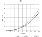
- FIG. 4 shows the input gradation values ( FIG. 3 is a diagram showing the relationship between CV) and a normalized output current value.
- the red light emitting element 21R, the green light emitting element 21G, and the blue light emitting element 21B have normalized output current values corresponding to each input gray level value (CV) from 0 gray level to 255 gray level. Since they have different curves showing the relationships between the two, they have different device characteristics.
- CV gray level value
- FIG. 5 shows an increase in the amount of accumulated current in each of the red light emitting element 21R shown in FIG. 3(a), the green light emitting element 21G shown in FIG. 3(b), and the blue light emitting element 21B shown in FIG.
- FIG. 3 is a diagram showing a tendency of luminance to decrease as
- the accumulated current amount of the red light emitting element 21R is an influence amount indicating the display influence of the red self-luminous pixel RPIX including the red light emitting element 21R
- the amount of accumulated current of the red light emitting element 21R is an influence amount indicating the display influence of the red self emitting pixel RPIX including the red light emitting element 21R
- the amount of accumulated current of the red light emitting element 21R is an influence amount indicating the display influence of the red self emitting pixel RPIX including the red light emitting element 21R.
- the value is calculated based on the display amount regarding the blue self-luminous pixel BPIX including 21B and the display amount regarding the red self-luminous pixel RPIX itself including the red light emitting element 21R arranged within the same display unit range.
- the amount of influence indicating the display influence of the red self-emitting pixel RPIX including the red light emitting element 21R is the same display amount as the display amount regarding the blue self emitting pixel BPIX including the blue light emitting element 21B arranged within the same display unit range.
- the accumulated current amount of the green light emitting element 21G is an influence amount indicating the display influence of the green self-luminous pixel GPIX including the green light emitting element 21G
- the amount of accumulated current of the green light emitting element 21G is an influence amount indicating the display influence of the green self emitting pixel GPIX including the green light emitting element 21G
- the amount of accumulated current of the green light emitting element 21G is an influence amount indicating the display influence of the green self emitting pixel GPIX including the green light emitting element 21G.
- the value is calculated based on the display amount regarding the blue self-luminous pixel BPIX including 21B and the display amount regarding the green self-luminous pixel GPIX itself including the green light emitting element 21G arranged within the same display unit range.
- the amount of influence indicating the display influence of the green self-luminous pixel GPIX including the green light emitting element 21G is the same display amount as the display amount regarding the blue self emitting pixel BPIX including the blue light emitting element 21B arranged within the same display unit range.
- the accumulated current amount of the blue light emitting element 21B is an influence amount indicating the display influence of the blue self-emitting pixel BPIX including the blue light emitting element 21B, and An example will be described in which the value is calculated based on the amount of display regarding the user, but the present invention is not limited to this.
- the influence amount indicating the display influence of the blue self-emitting pixel BPIX including the blue light emitting element 21B is the display amount regarding the blue self emitting pixel BPIX itself including the blue light emitting element 21B arranged within the same display unit range;
- the influence amount indicating the display influence of each color self-luminous pixel is, for example, the accumulated current amount and luminance according to the device characteristics of the red light emitting element 21R, the green light emitting element 21G, and the blue light emitting element 21B as shown in FIG. If the relationship of decrease is obtained in advance, the degree of decrease in brightness of each color light emitting element can be determined from the amount of accumulated current.
- the display amount for each color self-luminous pixel itself will be explained using, as an example, a case where the display amount for each color self-emitting pixel is a normalized output current value corresponding to each input gradation value (CV) shown in FIG. , but is not limited to this, and may be an input gradation value (CV).
- CV input gradation value
- the display amount regarding the blue self-luminous pixel BPIX is a correction coefficient described later calculated based on the normalized output current value corresponding to each input gradation value (CV) shown in FIG. will be described as an example, but the invention is not limited to this.
- the influence amount indicating the display influence of the red self-luminous pixel RPIX and the influence amount indicating the display influence of the green self-luminous pixel GPIX are set to the blue light emitting elements 21B arranged within the same display unit range.
- the explanation has been given as an example of a case where the calculation is performed by reflecting the display amount of the blue self-luminous pixel BPIX including
- Each influence amount indicating the display influence of the self-emissive pixel GPIX is displayed regarding the blue self-emissive pixel BPIX including the blue light emitting elements 21B arranged within a plurality of adjacent display unit ranges, as in Embodiment 2 described later. It may be calculated by reflecting the amount.
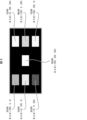
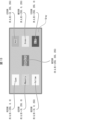
- FIG. 6 is a diagram showing an example of a burn-in display pattern.
- a C255 printing area C255R that performs display, an M255 printing area M255R that performs display with the gradation of each color self-emitting pixel in one display unit being (R, G, B) (255, 0, 255), and each color in one display unit.
- Each of the printing areas R255R, G255R, B255R, W255R, C255R, M255R, and Y255R can be set to a size that includes, for example, 10,000 self-emitting pixels, but the size is not limited to this, and each printing The size of the area can be set as appropriate.
- each burn-in area R255R, G255R, B255R, W255R, C255R, M255R, Y255R can be set to, for example, 100 hours, but is not limited to this, and each burn-in area is displayed. The time for this can be set as appropriate.
- the red light emitting element 21R included in the red self-emitting pixel RPIX, the green light emitting element 21G included in the green self-emitting pixel GPIX, and the blue self-emitting element 21G included in the blue self-emitting pixel BPIX The blue light emitting element 21B deteriorated and a decrease in brightness occurred.
- the amount of decrease in brightness of the red light emitting element 21R included in the red self-emitting pixel RPIX in the R255 burning area R255R and the amount of decrease in the brightness of the red light emitting element 21R included in the red self-emitting pixel RPIX in the W255 burning area W255R.
- the values should be the same, but in the actual display panel 2, a symptom occurred where the values were not the same.
- FIG. 7 shows the R255 burning region R255R shown in FIG. (for example, 100 hours) and after displaying the W255 burning area W255R shown in FIG. 6 for a predetermined time (for example, 100 hours).
- FIG. 7 shows the R255 burning region R255R shown in FIG. (for example, 100 hours) and after displaying the W255 burning area W255R shown in FIG. 6 for a predetermined time (for example, 100 hours).
- the brightness of the red light-emitting element 21R included in the red self-emission pixel RPIX in the R255 printing area R255R is compared to the initial brightness of the red light-emitting element 21R included in the red self-emission pixel RPIX of the display panel 2. Although the amount of decrease in the brightness of the red light emitting element 21R included in the red self-luminous pixel RPIX in the W255 printing area W255R is large.
- the red light emitting element 21R included in the red self-emitting pixel RPIX, the green light emitting element 21G included in the green self-emitting pixel GPIX, and the blue self-emitting element 21G included in the blue self-emitting pixel BPIX The blue light emitting element 21B deteriorated and a decrease in brightness occurred.
- the amount of decrease in the brightness of the green light emitting element 21G included in the green self-emitting pixel GPIX of the G255 burning area G255R and the amount of decrease in the brightness of the green light emitting element 21G included in the green self-emitting pixel GPIX of the W255 burning area W255R.
- the values should be the same, but in the actual display panel 2, a symptom occurred where the values were not the same.
- FIG. 8 shows the G255 burning area G255R shown in FIG. (For example, 100 hours) and after displaying the W255 burning area W255R shown in FIG. 6 for a predetermined time (For example, 100 hours)
- FIG. 8 shows the G255 burning area G255R shown in FIG. (For example, 100 hours) and after displaying the W255 burning area W255R shown in FIG. 6 for a predetermined time (For example, 100 hours)
- FIG. 8 shows the G255 burning area G255R shown in FIG. (For example, 100 hours) and after displaying the W255 burning area W255R shown in FIG. 6 for a predetermined time (For example, 100 hours)
- FIG. 8 shows the G255 burning area G255R shown in FIG. (For example, 100 hours) and after displaying the W255 burning area W255R shown in FIG. 6 for a predetermined time (For example, 100 hours)
- the brightness of the green light-emitting element 21G included in the green self-emission pixel GPIX of the G255 printing area G255R is compared to the initial brightness of the green light-emitting element 21G included in the green self-emission pixel GPIX of the display panel 2.
- the amount of decrease in the brightness of the green light emitting element 21G included in the green self-emitting pixel GPIX in the W255 printing area W255R is large, the brightness of the green light emitting element 21G included in the green self-emitting pixel GPIX in the W255 printing area W255R is slightly lower. The amount of decrease is greater.
- the red light emitting element 21R included in the red self-emitting pixel RPIX, the green light emitting element 21G included in the green self-emitting pixel GPIX, and the blue self-emitting element 21G included in the blue self-emitting pixel BPIX The blue light emitting element 21B deteriorated and a decrease in brightness occurred.
- the amount of decrease in the brightness of the blue light emitting element 21B included in the blue self-emitting pixel BPIX in the B255 burning area B255R, and the amount of decrease in the brightness of the blue light emitting element 21B included in the blue self-emitting pixel BPIX in the W255 burning area W255R. were equal, which could be called an ideal state.
- FIG. 9 shows the B255 burning area B255R shown in FIG. (For example, 100 hours) and after displaying the W255 burning area W255R shown in FIG. 6 for a predetermined time (For example, 100 hours)
- FIG. 9 shows the B255 burning area B255R shown in FIG. (For example, 100 hours) and after displaying the W255 burning area W255R shown in FIG. 6 for a predetermined time (For example, 100 hours)
- the brightness of the blue light emitting element 21B included in the blue self-emitting pixel BPIX in the B255 printing area B255R is Although the amount of decrease in the luminance of the blue light-emitting element 21B included in the blue self-luminous pixel BPIX in the W255 printing area W255R is large, both amounts of decrease are the same.
- the red light emitting element 21R included in the red self-emitting pixel RPIX, the green light emitting element 21G included in the green self-emitting pixel GPIX, and the blue light emitting element 21B included in the blue self-emitting pixel BPIX have different deterioration trends. .
- the amount of reduction in brightness of the red light emitting element 21R included in the red self-emitting pixel RPIX in the R255 burning area R255R and the amount of reduction in the brightness of the red light emitting element 21R included in the red self-emitting pixel RPIX in the W255 burning area W255R are also shown. The amount of reduction in brightness is different. Further, as shown in FIG.
- the amount of decrease in the brightness of the green light emitting element 21G included in the green self-emitting pixel GPIX in the G255 printing area G255R and the amount of reduction in the brightness of the green light emitting element 21G included in the green self-emitting pixel GPIX in the W255 printing area W255R are also shown.
- the amount of reduction in brightness is different.
- the relationship between the amount of accumulated current of the red light-emitting element 21R included in the red self-emission pixel RPIX and the luminance reduction which is an influence amount indicating the influence of the display of the red self-emission pixel RPIX
- the green self-emission The relationship between the amount of accumulated current of the green light-emitting element 21G included in the green self-luminous pixel GPIX, which is an influence amount indicating the influence of the display of the pixel GPIX, and the luminance reduction is obtained in the green monochromatic light emitting state, and these obtained data (the amount of accumulated current). If compensation is performed based on the relationship between brightness and luminance reduction, compensation can be performed normally in the red monochrome or green monochrome printing area, but compensation is insufficient in the W255 printing area W255R, resulting in brightness differences and coloring.
- the above-mentioned deterioration of the red light emitting element 21R included in the red self-emitting pixel RPIX in the W255 burning area W255R and the deterioration of the green light emitting element 21G included in the green self-emitting pixel GPIX in the W255 burning area W255R are caused by the fact that the element itself is turned on. It is considered that the process progresses more quickly when the blue light emitting element 21B included in the blue self-emitting pixel BPIX is lit at the same time.
- the degree of deterioration of the red light-emitting element 21R included in the red self-emission pixel RPIX is the same as that of the red light-emitting element 21R included in the red self-emission pixel RPIX of Since the blue light emitting element 21B included in the pixel BPIX is not lit, the degree of deterioration is equivalent to that of the green light emitting element 21G included in the green self-emitting pixel GPIX in the G255 printing area G255R.
- the amount of deterioration of the red light-emitting element 21R included in the red self-emission pixel RPIX and the green light-emitting element 21G included in the green self-emission pixel GPIX are determined. It can be seen that the amount of deterioration changes.
- the causes of such deterioration symptoms are thought to include multiple factors such as current leakage and crosstalk between self-emissive pixels, fluctuations in display panel temperature, and reflected light from surrounding self-emissive pixels.
- the symptoms of deterioration are thought to vary depending on the structure and manufacturing process of the display panel.
- the influence amount indicating the display influence of the red self-luminous pixel RPIX and the influence amount indicating the display influence of the green self-luminous pixel GPIX are compared to the blue light emitting pixel arranged within the same display unit range. It was calculated by reflecting the display amount regarding the blue self-luminous pixel BPIX including the element 21B.
- the control device 4 of the display panel 2 includes a storage section 5 and a compensation processing section 8.
- the storage section 5 includes an influence amount data calculation section 6 and an influence amount data storage section 7, and the compensation processing section 8 includes a compensation data calculation section 9, a first compensation data storage section 10, and a second compensation data storage section 11. and a compensator 12.
- the influence amount data calculation unit 6 includes an R current conversion value calculation unit 6a, a G current conversion value calculation unit 6b, a B current conversion value calculation unit 6c, and a correction coefficient calculation unit 6d.
- the input video signals of each color (red input video signal VIR, green input video signal VIG, blue input video signal VIB) having a predetermined gradation value (CV) are compensated by the compensator 12 to produce the compensated predetermined value.
- the corrected video signals for each color (red corrected video signal VIR', green corrected video signal VIG', and blue corrected video signal VIB') each have a gradation value (CV).
- the compensated predetermined gradation value (CV) is a signal amplified to compensate for the reduction in brightness, and is a signal that is amplified to compensate for a decrease in luminance, and is a signal that is amplified to compensate for a decrease in luminance.
- the current value flowing through each of the element 21G and the blue light emitting element 21B included in the blue self-luminous pixel BPIX is also amplified. For example, after an input video signal of each color having a gradation value (CV) of 0 to 255 is compensated by the compensation unit 12, it becomes a corrected video signal of each color having a gradation value (CV) greater than 255. In some cases.
- CV gradation value
- the R current conversion value calculation unit 6a converts the red corrected video signal VIR' having a predetermined compensated gradation value (CV) into an input gradation value (CV) of the red light emitting element 21R as shown in FIG. 4, for example. Using a look-up table (LUT) in which the relationship between the value and the normalized output current value is stored, it is converted into a normalized output current value which is data indicating the display amount CR of the red light emitting element 21R. That is, it is converted into a current value that actually flows when a voltage corresponding to a compensated predetermined gradation value (CV) is applied to the red light emitting element 21R.
- the present invention is not limited to this, and the R current conversion value calculation unit 6a may calculate the current value. Furthermore, the R current conversion value calculation unit 6a may convert the current value into a count value, for example, expressed in 7 bits, which corresponds to the output current value, so that the calculation is easy and the amount of memory is suppressed. good.
- the G current conversion value calculation unit 6b converts the green corrected video signal VIG' having a predetermined compensated gradation value (CV) into an input gradation value (CV) of the green light emitting element 21G as shown in FIG. 4, for example. Using a look-up table (LUT) in which the relationship between CG and the normalized output current value is stored, it is converted into a normalized output current value which is data indicating the display amount CG of the green light emitting element 21G. That is, it is converted into a current value that actually flows when a voltage corresponding to a compensated predetermined gradation value (CV) is applied to the green light emitting element 21G.
- the present invention is not limited to this, and the G current conversion value calculation unit 6b may calculate the current value. Furthermore, the G current conversion value calculation unit 6b may convert the current value into a count value, for example, expressed in 7 bits, which corresponds to the output current value, so that the current value can be easily calculated and the amount of memory can be suppressed. good
- the B current conversion value calculation unit 6c converts the blue corrected video signal VIB' having a predetermined compensated gradation value (CV) into an input gradation value (CV) of the blue light emitting element 21B as shown in FIG. 4, for example. Using a lookup table (LUT) in which the relationship between the value and the normalized output current value is stored, it is converted into a normalized output current value which is data indicating the display amount CB of the blue light emitting element 21B. That is, it is converted into a current value that actually flows when a voltage corresponding to a compensated predetermined gradation value (CV) is applied to the blue light emitting element 21B.
- the present invention is not limited to this, and the B current conversion value calculation unit 6c may calculate the current value. Furthermore, the B current conversion value calculation unit 6c may convert the current value into a count value, for example, expressed in 7 bits, which corresponds to the output current value, so that calculation is easy and the amount of memory can be suppressed. good.
- the correction coefficient calculation unit 6d uses the normalized output current value, which is data indicating the display amount CB of the blue light emitting element 21B converted by the B current conversion value calculation unit 6c, to calculate the value in the R current conversion value calculation unit 6a.
- a correction coefficient BCO1 for correcting the normalized output current value which is data indicating the converted display amount CR of the red light emitting element 21R, and a display amount CG of the green light emitting element 21G converted by the G current conversion value calculation unit 6b.
- a correction coefficient BCO2 is calculated for correcting the normalized output current value, which is data indicating .
- the case where normalized output current values are used as data indicating the display amounts CR, CG, and CB has been described as an example, but the present invention is not limited to this, and the display amounts CR, CG, and - A predetermined compensated gradation value (CV) may be used as is as data indicating CB.
- the compensated predetermined gradation value (CV) as data indicating the display amounts CR, CG, and CB as is, the R current conversion value calculation section 6a, the G current conversion value calculation section 6b, and the B current conversion
- the value calculation unit 6c may not be provided.
- FIG. 10 is a diagram showing an example of the correction coefficients BCO1 and BCO2 calculated by the correction coefficient calculation unit 6d of the influence amount data calculation unit 6 included in the display device 1 of the first embodiment.
- the correction coefficient calculation unit 6d calculates a correction coefficient as shown in FIG. 10 and a compensated predetermined gradation value (CV) or a normalized output current value, which is data indicating the display amount CB of the blue light emitting element 21B.
- the correction coefficients BCO1 and BCO2 may be derived using a look-up table (LUT) that stores the relationship between the two.
- a correction coefficient corresponding to the display amount CB of the blue light emitting element 21B is added to the normalized output current value, which is data indicating the display amount CR of the red light emitting element 21R.
- the value obtained by multiplying BCO1 is added to the influence amount data storage unit 7 (short-term storage memory (counter)), and the normalized output current value, which is data indicating the display amount CG of the green light emitting element 21G, is added to the blue light emitting element.
- the value obtained by multiplying the display amount CB of the blue light emitting element 21B by the correction coefficient BCO2 corresponding to the correction coefficient BCO2 is added to the influence amount data storage unit 7 (short-term storage memory (counter)), and the normal value which is the data indicating the display amount CB of the blue light emitting element 21B is obtained.
- the converted output current value is added to the influence amount data storage section 7 (short-term storage memory (counter)).
- the influence amount data storage section 7 (short-term storage memory (counter)) may be, for example, a frame memory.
- the normalized output current value which is data indicating the display amount CR of the red light emitting element 21R
- the accumulated value of the value obtained by multiplying the display amount CB by the correction coefficient BCO1 corresponding to the green light emitting element 21G is normalized as the influence amount data GD (accumulated current amount) of the green light emitting element 21G, which is data indicating the display amount CG of the green light emitting element 21G.
- the present invention is not limited to this. do not have.
- the display amount CR of the red light emitting element 21R is not considered as the influence amount data RD (accumulated current amount) of the red light emitting element 21R
- the normalized output current which is data indicating the display amount CR of the red light emitting element 21R.
- the value may be always fixed at 1, and an accumulated value obtained by multiplying this value by a correction coefficient BCO1 corresponding to the display amount CB of the blue light emitting element 21B may be used.
- the normalized output current value which is data indicating the display amount CG of the green light emitting element 21G, is always fixed to 1, and here the blue light emitting element 21B
- An accumulated value obtained by multiplying the display amount CB by a correction coefficient BCO2 corresponding to the display amount CB may be used.
- the compensation data calculation section 9 performs correction regarding the correction amount of the red light emitting element 21R based on the influence amount data RD (accumulated current amount) of the red light emitting element 21R from the influence amount data storage section 7 (short-term storage memory (counter)).
- Data RD' is calculated, and correction regarding the correction amount of the green light emitting element 21G is performed based on the influence amount data GD (accumulated current amount) of the green light emitting element 21G from the influence amount data storage section 7 (short-term storage memory (counter)).
- Data GD' is calculated, and correction regarding the correction amount of the blue light emitting element 21B is performed based on the influence amount data BD (accumulated current amount) of the blue light emitting element 21B from the influence amount data storage section 7 (short-term storage memory (counter)). Calculate data BD'.
- the compensation data calculation unit 9 uses a look-up table (LUT) that stores the relationship between the amount of accumulated current and the brightness of the red light emitting element 21R, the green light emitting element 21G, and the blue light emitting element 21B as shown in FIG. 5, for example. may be used to derive correction data RD' regarding the correction amount of the red light emitting element 21R, correction data GD' regarding the correction amount of the green light emitting element 21G, and correction data BD' regarding the correction amount of the blue light emitting element 21B. Note that the correction amount can be determined, for example, so that the initial brightness of each color light emitting element is achieved.
- LUT look-up table
- the correction data RD' regarding the correction amount of the red light emitting element 21R, the correction data GD' regarding the correction amount of the green light emitting element 21G, and the correction data BD' regarding the correction amount of the blue light emitting element 21B calculated in the compensation data calculation unit 9 are used for compensation.
- the data is stored in the first data storage section 10 and the compensation data second storage section 11.
- the second compensation data storage unit 11 is a backup storage unit for saving data when the display device 1 is powered off, and can be configured with a flash memory, for example, and can be provided as needed. All you have to do is stay there.
- correction data RD' regarding the correction amount of the red light emitting element 21R, correction data GD' regarding the correction amount of the green light emitting element 21G, and correction data regarding the correction amount of the blue light emitting element 21B are stored in the compensation data first storage unit 10.
- each color input video signal red input video signal VIR, green input video signal VIG, blue input video signal VIB
- CV predetermined gradation value
- W255R reflects an amplified amount of compensation rather than monochromatic deterioration, which eliminates the lack of compensation in W255 burn area W255R, C255 burn area C255R, and M255 burn area M255R, suppressing brightness level difference and color shift. be able to.
- the correction data RD' regarding the correction amount of the red light emitting element 21R, the correction data GD' regarding the correction amount of the green light emitting element 21G, and the correction data BD' regarding the correction amount of the blue light emitting element 21B calculated in the compensation data calculation unit 9 are as follows. , the amount of correction in the positive direction to compensate for the reduction in luminance of the red light emitting element 21R, the green light emitting element 21G, and the blue light emitting element 21B. If an increase occurs, the correction amount may be in the negative direction. That is, any correction amount that compensates for changes over time may be used.
- the deterioration of the red light emitting element 21R included in the red self-luminous pixel RPIX in the W255 burning area W255R shown in FIG. progresses more quickly when the blue light-emitting element 21B included in the blue self-luminous pixel BPIX is lit at the same time as the blue self-luminous pixel BPIX itself is lit.
- the red light emitting element 21R included in the red self-emitting pixel RPIX is not lit.
- the normalized data indicating the display amount CR of the red light emitting element 21R is It is preferable to use 0 as the normalized output current value, which is data indicating the output current value and the display amount CG of the green light emitting element 21G.
- the influence amount data storage section 7 provided in the storage section 5 is capable of accumulating the influence amount data of the self-emissive pixels in the state of outputting light among the red self-emissive pixels RPIX and the green self-emissive pixels GPIX. preferable.
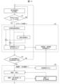
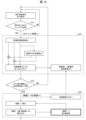
- FIG. 11 is a flow diagram showing the steps from the influence amount data accumulation process (S2) to the compensation data update process (S4) performed in the control device 4 included in the display device 1 of the first embodiment.
- the updated influence amount data RD of the red light emitting element 21R Influence amount data GD (accumulated current amount) of the green light emitting element 21G (accumulated current amount), and influence amount data BD (accumulated current amount) of the blue light emitting element 21B can be obtained.
- the influence amount data RD (accumulated current amount) of the red light emitting element 21R newly obtained in the influence amount data accumulation process (S2) and the influence amount data GD (accumulated amount) of the green light emitting element 21G are calculated. It is determined for each self-emitting pixel of each color whether the influence amount data BD (current amount) and the influence amount data BD (accumulated current amount) of the blue light emitting element 21B are equal to or greater than a threshold value.
- Influence amount data RD (accumulated current amount) of the red light emitting element 21R newly obtained in the influence amount data accumulation process (S2)
- influence amount data GD (accumulated current amount) of the green light emitting element 21G
- influence of the blue light emitting element 21B If the amount data BD (accumulated current amount) exceeds a preset threshold, it is determined that the deterioration has progressed to some extent, and the process proceeds to compensation data updating processing (S4).
- the value of the influence amount data storage unit (short-term storage memory) is reset and new storage is started. Further, the compensation data, that is, the correction data RD' regarding the correction amount of the red light emitting element 21R, the correction data GD' regarding the correction amount of the green light emitting element 21G, and the correction data BD' regarding the correction amount of the blue light emitting element 21B are set to the threshold value. In addition, a value corresponding to a correction voltage that can obtain the target brightness may be calculated based on the current compensation data and considering how far the deterioration has progressed. The compensation data may be simply calculated by adding a predetermined value determined by the threshold value.
- the amount to be added is determined by calculating the amount based on the current compensation data value, or it is determined by using a look-up table (LUT). You may also do so.
- the influence amount data accumulation process (S2) is performed, for example, every 15 frames has been described as an example, but the present invention is not limited to this, and for example, the influence amount data
- the data accumulation process (S2) may be performed for every frame.
- the compensation data update process (S4) may also be performed, for example, every frame.
- a control device for a display panel 2 that can perform correction that accurately reflects the level of change over time (deterioration) due to the influence of adjacent pixels by checking the current value flowing through the light emitting element or the voltage value applied to the light emitting element. 4 and the control method for the display panel 2 can be confirmed.
- the display area DA of the display panel 2 there is a first area consisting of 10,000 self-emitting pixels (100 vertically x 100 horizontally), and a first area consisting of 10,000 self-luminous pixels (100 vertically x 100 horizontally).
- Each of the second areas composed of pixels can be displayed in a burn-in display pattern described below. Note that the first area and the second area displayed in the display area DA of the display panel 2 are preferably separated by a predetermined distance, but may be continuous areas.
- the display may continue.
- the minimum gradation value is 0 gradation
- the maximum gradation value is 255 gradation, but this is not limiting. do not have.
- the luminous efficiency of the red light emitting element 21R provided in the red self-luminous pixel RPIX included in the second area does not deteriorate. , which is larger than the deterioration of the luminous efficiency of the red light emitting element 21R included in the red self-luminous pixel RPIX included in the first region.
- the display A control device 4 provided in the device 1 controls current flowing through the red self-emitting pixel RPIX included in the first region, that is, the red light emitting element 21R provided in the red self-emitting pixel RPIX included in the first region. Also, the current flowing through the red self-luminous pixel RPIX included in the second region, that is, the red light emitting element 21R provided in the red self-luminous pixel RPIX included in the second region is increased.
- each of the red self-emissive pixels RPIX included in the first area and the red self-emissive pixels RPIX included in the second area is Although the case where the display is performed in gradations has been described as an example, the present invention is not limited to this.
- the red self-luminous pixel RPIX and the green self-luminous pixel GPIX included in the first region and the red self-luminous pixel GPIX included in the second region When each of the pixel RPIX and the green self-luminous pixel GPIX is displayed in 255 gradations, or the red self-luminous pixel RPIX, the green self-luminous pixel GPIX and the blue self-luminous pixel BPIX included in the first area and the second
- the control device 4 provided in the display device 1 controls the first The red self-luminous pixel RPIX and the green self-luminous pixel GPIX included in the region, that is, the red light-emitting element 21R included in the red self-luminous pixel RPIX included in the first region and
- the red self-emissive pixel RPIX and the green self-emissive pixel GPIX included in the second region that is, the red self-emissive pixel RPIX included in the second region, the red light emitting element 21R and Increase the current flowing through the green light emitting element 21G provided in the green self-luminous pixel GPIX.
- FIGS. 12 to 16 a second embodiment of the present disclosure will be described based on FIGS. 12 to 16.
- the control device 4' included in the display device 1' of this embodiment is different from the first embodiment described above in that it includes a two-dimensional correction coefficient calculation unit 6d' and a delay line memory 28. .
- Other details are as described in the first embodiment.
- members having the same functions as those shown in the drawings of Embodiment 1 are given the same reference numerals, and the explanation thereof will be omitted.
- FIG. 12 is a diagram showing a schematic configuration of a display panel 2' provided in a display device 1' of Embodiment 2 and a control device 4' of the display panel 2'.
- the display device 1' of the present embodiment can light up the blue light emitting element 21B included in the blue self-emitting pixel BPIX for a long time, so that the light emitting element included in the self-emitting pixel in an area several display units away can be illuminated.
- the control device 4' includes a two-dimensional correction coefficient calculating section 6d'. The occurrence and severity of these deterioration symptoms vary depending on the structure of the display panel's self-luminous pixels, the amount of current flowing through the light-emitting elements included in the self-luminous pixels, and the environmental temperature.
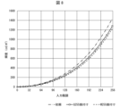
- a high current (a high current such that the maximum white brightness of the display panel is 1000 nits) continues to flow for a long time (for example, 1000 hours) at a temperature of (for example, 85 degrees Celsius)
- a temperature of for example, 85 degrees Celsius
- multiple blue light emitting elements 21B are turned on. Deterioration such as bleeding occurs even in the periphery of the area, that is, in the non-lighting area, which is about ten or more self-emitting pixels away from the boundary of the area where the plurality of blue light emitting elements 21B are turned on.
- FIG. 13 is a diagram showing an ideal burned-in display state when a gray display is performed on the entire surface after the burned-in display pattern shown in FIG. 6 is displayed for a predetermined period of time (for example, several hundred hours).
- the red light emitting element 21R included in the red self-luminous pixel RPIX has deteriorated and the brightness has decreased, so the color appears to be a pale cyan color.
- the green light emitting element 21G included in the green self-luminous pixel GPIX has deteriorated and the brightness has decreased, so that the color appears to be a pale magenta color.
- the blue light emitting element 21B included in the blue self-luminous pixel BPIX has deteriorated and the brightness has decreased, so that the color appears to be a pale yellowish color.
- the green light emitting element 21G included in the green self-emitting pixel GPIX and the blue light emitting element 21B included in the blue self-emitting pixel BPIX have deteriorated and the brightness has decreased, so the color is changed to a pale red color. I can see it.
- the red light emitting element 21R included in the red self-emitting pixel RPIX and the blue light emitting element 21B included in the blue self-emitting pixel BPIX have deteriorated and the brightness has decreased, so the color is changed to a pale greenish color. I can see it.
- the red light emitting element 21R included in the red self-emitting pixel RPIX and the green light emitting element 21G included in the green self-emitting pixel GPIX have deteriorated and the brightness has decreased, so the color is a pale blue color. I can see it.
- the red light emitting element 21R included in the red self-emitting pixel RPIX, the green light emitting element 21G included in the green self-emitting pixel GPIX, and the blue light emitting element 21B included in the blue self-emitting pixel BPIX deteriorate and the brightness decreases. As a result, the area appears darker gray than the area where burn-in has not occurred.
- FIG. 14(a), FIG. 14(b), and FIG. 14(c) are examples of the results of an aging (burn-in) test of the display panel 2' conducted by the inventors of the present disclosure. Note that the display panel 2' used here has different characteristics from the display panel 2 used in the aging (burn-in) test conducted in connection with Embodiment 1, so the results of the aging (burn-in) test are also different.
- FIG. 14(a) is a diagram showing a display state when a monochromatic red display is performed on the entire surface after the burned-in display pattern shown in FIG. b) is a diagram showing a display state when a monochromatic green display is performed on the entire surface after the burned-in display pattern shown in FIG. 6 has been displayed for a predetermined time (for example, several hundred hours), and (c) of FIG. FIG. 7 is a diagram showing a display state when a monochromatic blue display is performed on the entire surface after the burned-in display pattern shown in FIG. 6 is displayed for a predetermined period of time (for example, several hundred hours).
- Deterioration symptoms such as blurring occur when a printed area including a plurality of blue light emitting elements 21B continues to be lit, and the red light emitting elements 21R and green self emitting pixels included in the surrounding red self emitting pixels RPIX that are not lit. This occurs because the green light emitting element 21G included in GPIX deteriorates.
- the presence or absence of such deterioration symptoms and the extent of their impact on the surrounding area vary depending on the structure and manufacturing process of the display panel's self-luminous pixels, the optical film and glass provided on the entire surface, and the aging conditions (brightness, temperature). .
- the symptoms shown in FIGS. 14(a), 14(b), and 14(c) are examples of symptoms when aging is applied for a long time under certain conditions.
- the burn-in display pattern shown in FIG. 6 is displayed for a predetermined period of time (for example, several hundred hours) and then a red monochrome display is performed on the entire surface, the R255 burn-in area R255R and the Y255 burn-in area Y255R In , the red light emitting element 21R included in the red self-luminous pixel RPIX has deteriorated and the brightness has decreased, so that burn-in due to the brightness decrease in the rectangular shape is observed.
- a predetermined period of time for example, several hundred hours
- the burning areas B255R, W255R, C255R, and M255R are There is a blur-like reduction in brightness in the periphery.
- the blue light emitting element 21B is turned on and aging, the red light emitting element 21R included in the red self-luminous pixel RPIX is also affected in some way and deterioration progresses.
- no deterioration such as bleeding is observed in the Y255 printing area Y255R, it can be said that there is no effect even if the green light emitting element 21G is turned on and aged.
- the burn-in display pattern shown in FIG. 6 is displayed for a predetermined period of time (for example, several hundred hours) and then a green monochrome display is performed on the entire surface, the G255 burn-in area G255R and the Y255 burn-in area Y255R In , the green light emitting element 21G included in the green self-luminous pixel GPIX has deteriorated and the brightness has decreased, so that burn-in due to the brightness decrease in the rectangular shape is observed.
- a predetermined period of time for example, several hundred hours
- the burning areas B255R, W255R, C255R, and M255R are There is a blur-like reduction in brightness in the periphery.
- the green light emitting element 21G included in the green self-luminous pixel GPIX is also affected in some way and deterioration progresses. Further, since no deterioration such as bleeding is observed in the Y255 baking area Y255R, it can be said that aging while lighting the red light emitting element 21R has no effect.
- the control device 4' included in the display device 1' shown in FIG. 12 includes a two-dimensional correction coefficient calculation unit 6d' in order to improve the blurring that occurs around the printing area described above.
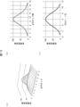
- FIG. 15A is a diagram showing the degree of influence that a certain self-emissive pixel (the blue light-emitting element 21B included in the blue self-emissive pixel BPIX) has on surrounding self-emissive pixels in the horizontal and vertical directions.
- FIG. 15(b) is a diagram showing the degree of influence that a certain self-emissive pixel (the blue light-emitting element 21B included in the blue self-emissive pixel BPIX) has on surrounding self-emissive pixels in the horizontal direction.
- 15(c) is a diagram showing the degree of influence that a certain self-emissive pixel (the blue light-emitting element 21B included in the blue self-emissive pixel BPIX) has on surrounding self-emissive pixels in the vertical direction.
- the influence of a certain self-emissive pixel (the blue light-emitting element 21B included in the blue self-emissive pixel BPIX) on the surrounding self-emissive pixels is grasped in advance, and for example, the blue light-emitting element included in one blue self-emissive pixel BPIX is
- the range and degree of influence that 21B has on surrounding self-luminous pixels can be created as a two-dimensional lookup table (LUT) of 17 taps horizontally by 11 taps vertically, as shown in FIG. 15(a). Note that here, the number of taps means the number of self-emitting pixels. As shown in FIGS.
- the influence amount indicating the influence of display regarding each self-emissive pixel is determined by the distance between the particular self-emissive pixel (the blue light-emitting element 21B included in the blue self-emissive pixel BPIX) and each of the surrounding self-emissive pixels. It is preferable that the calculation be made such that the larger the value, the smaller the influence of the particular self-emitting pixel (the blue light-emitting element 21B included in the blue self-emitting pixel BPIX) on the influence amount.
- the two-dimensional correction coefficients BCO1' and BCO2' can be calculated using the degree coefficients.
- the two-dimensional correction coefficients BCO1' and BCO2' can be calculated using the influence coefficients. More specifically, the influence coefficient of the two-dimensional lookup table (LUT) shown in (a) of FIG. By multiplying, two-dimensional correction coefficients BCO1' and BCO2' are calculated. Then, a convolution operation is performed in which each value of the two-dimensional correction coefficients BCO1' and BCO2' is added to the display amount CR of the red light emitting element 21R or the display amount CG of the green light emitting element 21G at the target coordinates.
- the influence amount data calculation unit 6' calculates a value obtained by adding a two-dimensional correction coefficient BCO1' to the normalized output current value, which is data indicating the display amount CR of the red light emitting element 21R. , is added to the influence amount data storage unit 7 (short-term storage memory (counter)), and the two-dimensional correction coefficient BCO2' is added to the normalized output current value, which is data indicating the display amount CG of the green light emitting element 21G.
- the value is added to the influence amount data storage section 7 (short-term storage memory (counter)), and the normalized output current value, which is data indicating the display amount CB of the blue light emitting element 21B, is added to the influence amount data storage section 7 (short-term storage memory (counter)).
- the delay line memory 28 stores the corrected video signals VIR' and VIG', and the R current conversion value calculation section 6a and the G current conversion value calculation section 6b calculate the two-dimensional correction coefficients BCO1' and BCO2'.
- the corrected video signals VIR' and VIG' regarding the self-emitting pixels are sequentially read out from the delay line memory 28, and the amount of accumulated current is converted.
- two-dimensional correction coefficient calculation unit 6d' for example, a line memory capable of handling 11 vertical taps is prepared, and two-dimensional correction coefficients BCO1' and BCO2' are calculated using a two-dimensional lookup table (LUT). You may.
- the influence of deterioration from the blue light-emitting element 21B included in the blue self-emission pixel BPIX is the effect of deterioration from the red light-emitting element 21R included in the red self-emission pixel RPIX and the green light-emitting element 21G included in the green self-emission pixel GPIX.
- the value obtained by adding the two-dimensional correction coefficient BCO1' to the normalized output current value which is data indicating the display amount CR of the red light emitting element 21R, is used as the influence amount data.
- the value obtained by adding the two-dimensional correction coefficient BCO2' to the normalized output current value, which is data indicating the display amount CG of the green light emitting element 21G, is added to the storage unit 7 (short-term storage memory (counter)) and It is added to the amount data storage section 7 (short-term storage memory (counter)).
- FIG. 16 is a flow diagram showing the steps from the influence amount data accumulation process (S12) to the compensation data update process (S14) performed in the control device 4' included in the display device 1' of the second embodiment.
- the accumulation cycle determination process (S11) shown in FIG. 16 is the same as the accumulation cycle determination process (S1) described above in the first embodiment, and the count value determination process (S13) shown in FIG. This is the same as the count value determination process (S3), and the compensation data update process (S14) shown in FIG. 16 is the same as the compensation data update process (S4) described above in the first embodiment. omitted.
- the above-described process is performed based on FIG. As described above, for each self-emitting pixel of each color, the two-dimensional correction coefficient BCO1' corresponding to the display amount CB of the blue light emitting element 21B is added to the normalized output current value, which is data indicating the display amount CR of the red light emitting element 21R.
- the normalized output current value, which is data indicating the display amount CB of the blue light emitting element 21B, is calculated and added (counted) to the influence amount data storage unit (short-term storage memory), thereby updating the It is possible to obtain influence amount data RD (accumulated current amount) of the red light emitting element 21R, influence amount data GD (accumulated current amount) of the green light emitting element 21G, and influence amount data BD (accumulated current amount) of the blue light emitting element 21B.
- Embodiment 3 of the present disclosure will be described based on FIG. 17.
- the display panel 2'' included in the display device 1'' of the present embodiment is equipped with a temperature sensor 30, and the two-dimensional correction coefficient calculation unit 6d' receives temperature sensor information SIN from the temperature sensor 30.
- This embodiment differs from the second embodiment described above in that the two-dimensional correction coefficients BCO1'' and BCO2'' are calculated based on .
- Other details are as described in the second embodiment. For convenience of explanation, members having the same functions as those shown in the drawings of the second embodiment are designated by the same reference numerals, and the explanation thereof will be omitted.
- FIG. 17 is a diagram showing a schematic configuration of a display panel 2'' provided in a display device 1'' of Embodiment 3 and a control device 4'' of the display panel 2''.
- the display panel 2'' included in the display device 1'' is equipped with a temperature sensor 30. Then, in the two-dimensional correction coefficient calculation unit 6d' provided in the control device 4'' of the display panel 2'', the two-dimensional correction coefficients BCO1'' and BCO2 are calculated based on the temperature sensor information SIN from the temperature sensor 30. '' is calculated.
- the amount of current flowing through the light emitting elements of each color increases or decreases depending on the temperature state of the display panel 2'' (the higher the temperature, the more the amount of current flowing). Therefore, for example, a temperature sensor 30 is provided around or on the back of the display panel 2'', and based on the temperature sensor information SIN from the temperature sensor 30, the two-dimensional correction coefficient calculation unit 6d' calculates the two-dimensional correction coefficient BCO1'. It is preferable to calculate ' ⁇ BCO2''.
- the two-dimensional correction coefficients BCO1'' and BCO2'' are calculated in the two-dimensional correction coefficient calculation unit 6d' based on temperature sensor information SIN from the temperature sensor 30.
- the present invention is not limited thereto, and the correction coefficients BCO1 and BCO2 may be calculated in the correction coefficient calculation unit 6d described above in the first embodiment based on the temperature sensor information SIN from the temperature sensor 30.
- the influence of the blue light-emitting element 21B included in the blue self-emission pixel BPIX on the red light-emitting element 21R included in the red self-emission pixel RPIX, which is a surrounding self-emission pixel, and the green light-emitting element 21G included in the green self-emission pixel GPIX is as follows.
- the degree of influence differs depending on the temperature of the display panels 2, 2', and 2''. For example, when the temperature of the display panel 2, 2', 2'' is high, the range of self-emitting pixels that are affected tends to expand, and the amount of deterioration tends to increase.
- the two-dimensional look-up table (LUT) described above in Embodiment 2 is created in accordance with the maximum range of self-emitting pixels that are thermally affected, and the display panels 2, 2', 2' Based on the temperature sensor information SIN from the temperature sensor 30 provided in ', the two-dimensional correction coefficient from the two-dimensional look-up table (LUT) may be further multiplied by a temperature coefficient and used.
- the temperature coefficient of all self-emitting pixels within the maximum range of thermally affected self-emitting pixels is set to 100, and if it is 25 degrees Celsius or less, the thermally affected self-emitting pixels
- the temperature coefficients of all self-emissive pixels within the maximum range of emissive pixels may be set to zero.
- a display panel control device including a plurality of first self-emissive pixels that output a first color light and a plurality of second self-emissive pixels that output a second color light different from the first color light, Each of the plurality of first self-emissive pixels is arranged within a predetermined range with respect to the corresponding second self-emissive pixel of the plurality of second self-emissive pixels, a second self-emissive pixel corresponding to the first self-emissive pixel, calculated based on a display amount of the first self-emissive pixel arranged within the predetermined range with respect to the second self-emissive pixel; an accumulation unit that accumulates an influence amount indicating the influence of the display; a compensation processing unit that generates a corrected video signal by compensating for the temporal change of each of the second self-emissive pixels based on the influence amount regarding each of the plurality of second self-emissive pixels with respect to the input video signal;
- the influence amount regarding each of the plurality of second self-emissive pixels is determined by the amount of display regarding the first self-emissive pixel arranged within the predetermined range with respect to each of the second self-emissive pixels, and the amount of influence regarding each of the second self-emissive pixels.
- the amount of influence regarding each of the plurality of second self-emissive pixels is such that the larger the distance between the second self-emissive pixel and the first self-emissive pixel arranged within the predetermined range, the more The control device according to any one of aspects 1 to 3, wherein the control device is calculated such that the display amount for one self-luminous pixel has a small influence on the influence amount.
- the first colored light has a shorter wavelength than the second colored light
- the storage unit further accumulates an influence amount indicating the influence of display regarding each of the plurality of first self-emissive pixels calculated based on the display amount regarding the first self-emissive pixel itself
- the compensation processing unit further performs compensation for the temporal change of each of the first self-emissive pixels on the input video signal based on the influence amount regarding each of the plurality of first self-emissive pixels, thereby producing a corrected video signal.
- the control device according to any one of aspects 1 to 4, which generates.
- the first colored light is blue light;
- the control device according to any one of aspects 1 to 5, wherein the second color light is red light or green light.
- a control device according to any one of aspects 1 to 8, the display panel; a display control unit that displays on the display panel based on the corrected video signal; A display device equipped with
- the display panel includes a sensor that measures the temperature of the display panel, The display device according to aspect 9, wherein in the control device, the influence amount is calculated to increase as the temperature measured by the sensor increases.
- Each of the plurality of first self-emissive pixels of the display panel includes a first self-emissive element
- Each of the plurality of second self-emissive pixels of the display panel includes a second self-emissive element
- the display device according to aspect 10 wherein each of the first self-luminous element and the second self-luminous element includes an organic luminescent layer or a luminescent layer containing quantum dots.
- a method for controlling a display panel including a plurality of first self-emissive pixels that output a first color light and a plurality of second self-emissive pixels that output a second color light different from the first color light comprising: Each of the plurality of first self-emissive pixels is arranged within a predetermined range with respect to the corresponding second self-emissive pixel of the plurality of second self-emissive pixels, a second self-emissive pixel corresponding to the first self-emissive pixel, calculated based on a display amount of the first self-emissive pixel arranged within the predetermined range with respect to the second self-emissive pixel; an accumulation step of accumulating an influence amount indicating the influence of the display; a compensation processing step of generating a corrected video signal by compensating for the temporal change of each of the second self-emissive pixels based on the influence amount regarding each of the plurality of second self-emissive pixels with respect to the input video signal; How to
- the influence amount regarding each of the plurality of second self-emissive pixels is determined by the influence amount regarding the first self-emissive pixel arranged within the predetermined range with respect to each of the second self-emissive pixels.
- a control device for a display panel including a first self-emissive pixel that outputs a first color light and a second self-emissive pixel that outputs a second color light different from the first color light,
- the first self-emissive pixels are set to the minimum gradation value and the second self-emissive pixels are In addition to displaying pixels at the maximum gradation value for a predetermined time,
- the first self-emissive pixels and the second self-emissive pixels After displaying each of the self-emitting pixels at the maximum gradation value for the predetermined time, When each of the second self-emissive pixels included in the first area and the second self-emissive pixels included in the second area are displayed at
- the present disclosure can be used in a display panel control device, a display device, and a display panel control method.
Landscapes
- Engineering & Computer Science (AREA)
- Physics & Mathematics (AREA)
- Computer Hardware Design (AREA)
- General Physics & Mathematics (AREA)
- Theoretical Computer Science (AREA)
- Electroluminescent Light Sources (AREA)
Abstract
Description
第1色光を出力する複数の第1の自発光画素と、前記第1色光とは異なる第2色光を出力する複数の第2の自発光画素を含む表示パネルの制御装置であって、
前記複数の第1の自発光画素のそれぞれは、前記複数の第2の自発光画素のうちの対応する前記第2の自発光画素に対して所定範囲内に配置され、
前記第2の自発光画素に対して前記所定範囲内に配置された前記第1の自発光画素に関する表示量に基づき算出された、当該第1の自発光画素に対応する第2の自発光画素の表示の影響を示す影響量を蓄積する蓄積部と、
入力映像信号に対し、前記複数の第2の自発光画素それぞれに関する前記影響量に基づき前記第2の自発光画素のそれぞれの経時変化に対する補償を行って補正映像信号を生成する補償処理部と、を備えている。
第1色光を出力する複数の第1の自発光画素と、前記第1色光とは異なる第2色光を出力する複数の第2の自発光画素を含む表示パネルの制御方法であって、
前記複数の第1の自発光画素のそれぞれは、前記複数の第2の自発光画素のうちの対応する前記第2の自発光画素に対して所定範囲内に配置され、
前記第2の自発光画素に対して前記所定範囲内に配置された前記第1の自発光画素に関する表示量に基づき算出された、当該第1の自発光画素に対応する第2の自発光画素の表示の影響を示す影響量を蓄積する蓄積工程と、
入力映像信号に対し、前記複数の第2の自発光画素それぞれに関する前記影響量に基づき前記第2の自発光画素のそれぞれの経時変化に対する補償を行って補正映像信号を生成する補償処理工程と、を含む。
第1色光を出力する第1の自発光画素と、前記第1色光とは異なる第2色光を出力する第2の自発光画素を含む表示パネルの制御装置であって、
前記表示パネル上で所定数の前記第1の自発光画素および前記第2の自発光画素を含む第1領域において、前記第1の自発光画素を最小階調値で、前記第2の自発光画素を最大階調値で、所定時間表示すると共に、
前記表示パネル上で前記所定数の前記第1の自発光画素および前記第2の自発光画素を含み前記第1領域とは異なる第2領域において、前記第1の自発光画素および前記第2の自発光画素のそれぞれを前記最大階調値で、前記所定時間表示した後、
前記第1領域に含まれる前記第2の自発光画素および前記第2領域に含まれる前記第2の自発光画素のそれぞれを前記最大階調値で表示した場合、前記第1領域に含まれる前記第2の自発光画素に流す電流より、前記第2領域に含まれる前記第2の自発光画素に流す電流を多くする。
図1は、実施形態1の表示装置1に備えられた表示パネル2と表示パネル2の制御装置4との概略的な構成を示す図である。
次に、図12から図16に基づき、本開示の実施形態2について説明する。本実施形態の表示装置1’に備えられた制御装置4’には、2次元補正係数算出部6d’と遅延用ラインメモリ28とが備えられている点において、上述した実施形態1とは異なる。その他については実施形態1において説明したとおりである。説明の便宜上、実施形態1の図面に示した部材と同じ機能を有する部材については、同じ符号を付し、その説明を省略する。
次に、図17に基づき、本開示の実施形態3について説明する。本実施形態の表示装置1’’に備えられた表示パネル2’’には温度センサー30が備えられており、2次元補正係数算出部6d’においては、温度センサー30からの温度センサーの情報SINに基づき、2次元補正係数BCO1’’・BCO2’’が算出される点において、上述した実施形態2とは異なる。その他については実施形態2において説明したとおりである。説明の便宜上、実施形態2の図面に示した部材と同じ機能を有する部材については、同じ符号を付し、その説明を省略する。
〔態様1〕
第1色光を出力する複数の第1の自発光画素と、前記第1色光とは異なる第2色光を出力する複数の第2の自発光画素を含む表示パネルの制御装置であって、
前記複数の第1の自発光画素のそれぞれは、前記複数の第2の自発光画素のうちの対応する前記第2の自発光画素に対して所定範囲内に配置され、
前記第2の自発光画素に対して前記所定範囲内に配置された前記第1の自発光画素に関する表示量に基づき算出された、当該第1の自発光画素に対応する第2の自発光画素の表示の影響を示す影響量を蓄積する蓄積部と、
入力映像信号に対し、前記複数の第2の自発光画素それぞれに関する前記影響量に基づき前記第2の自発光画素のそれぞれの経時変化に対する補償を行って補正映像信号を生成する補償処理部と、を備えている制御装置。
前記複数の第2の自発光画素それぞれに関する前記影響量は、前記第2の自発光画素のそれぞれに対して前記所定範囲内に配置された前記第1の自発光画素に関する表示量と、当該第2の自発光画素それ自身に関する表示量とに基づき算出される、態様1に記載の制御装置。
前記蓄積部は、前記複数の第2の自発光画素のうち前記第2色光を出力している状態の前記第2の自発光画素の前記影響量を蓄積する、態様1または2に記載の制御装置。
前記複数の第2の自発光画素それぞれに関する前記影響量は、当該第2の自発光画素と前記所定範囲内に配置された前記第1の自発光画素との間の距離が大きい程、前記第1の自発光画素に関する表示量が前記影響量に及ぼす影響が小さくなるように算出される、態様1から3の何れかに記載の制御装置。
前記第1色光は前記第2色光より短波長の光であり、
前記蓄積部は、当該第1の自発光画素それ自身に関する表示量に基づき算出された前記複数の第1の自発光画素それぞれに関する表示の影響を示す影響量をさらに蓄積し、
前記補償処理部は、前記入力映像信号に対し、前記複数の第1の自発光画素それぞれに関する前記影響量に基づき前記第1の自発光画素のそれぞれの経時変化に対する補償をさらに行って補正映像信号を生成する、態様1から4の何れかに記載の制御装置。
前記第1色光は青色光であり、
前記第2色光は赤色光または緑色光である、態様1から5の何れかに記載の制御装置。
前記第1色光は前記第2色光より長波長の光である、態様1から4の何れかに記載の制御装置。
前記表示量は、前記自発光画素に流した電流量に関するデータである、態様1から7の何れかに記載の制御装置。
態様1から8の何れかに記載の制御装置と、
前記表示パネルと、
前記補正映像信号に基づき前記表示パネルに表示を行う表示制御部と、
を備えた表示装置。
前記表示パネルは、前記表示パネルの温度を測定するセンサーを備えており、
前記制御装置において、前記影響量は、前記センサーで測定された温度が高い程、大きくなるように算出される、態様9に記載の表示装置。
前記表示パネルの前記複数の第1の自発光画素のそれぞれは、第1自発光素子を備えており、
前記表示パネルの前記複数の第2の自発光画素のそれぞれは、第2自発光素子を備えており、
前記第1自発光素子及び前記第2自発光素子のそれぞれは、有機発光層または量子ドットを含む発光層を含む、態様10に記載の表示装置。
第1色光を出力する複数の第1の自発光画素と、前記第1色光とは異なる第2色光を出力する複数の第2の自発光画素を含む表示パネルの制御方法であって、
前記複数の第1の自発光画素のそれぞれは、前記複数の第2の自発光画素のうちの対応する前記第2の自発光画素に対して所定範囲内に配置され、
前記第2の自発光画素に対して前記所定範囲内に配置された前記第1の自発光画素に関する表示量に基づき算出された、当該第1の自発光画素に対応する第2の自発光画素の表示の影響を示す影響量を蓄積する蓄積工程と、
入力映像信号に対し、前記複数の第2の自発光画素それぞれに関する前記影響量に基づき前記第2の自発光画素のそれぞれの経時変化に対する補償を行って補正映像信号を生成する補償処理工程と、を含む、表示パネルの制御方法。
前記蓄積工程においては、前記複数の第2の自発光画素それぞれに関する前記影響量は、前記第2の自発光画素のそれぞれに対して前記所定範囲内に配置された前記第1の自発光画素に関する表示量と、当該第2の自発光画素それ自身に関する表示量とに基づき算出される、態様12に記載の表示パネルの制御方法。
第1色光を出力する第1の自発光画素と、前記第1色光とは異なる第2色光を出力する第2の自発光画素を含む表示パネルの制御装置であって、
前記表示パネル上で所定数の前記第1の自発光画素および前記第2の自発光画素を含む第1領域において、前記第1の自発光画素を最小階調値で、前記第2の自発光画素を最大階調値で、所定時間表示すると共に、
前記表示パネル上で前記所定数の前記第1の自発光画素および前記第2の自発光画素を含み前記第1領域とは異なる第2領域において、前記第1の自発光画素および前記第2の自発光画素のそれぞれを前記最大階調値で、前記所定時間表示した後、
前記第1領域に含まれる前記第2の自発光画素および前記第2領域に含まれる前記第2の自発光画素のそれぞれを前記最大階調値で表示した場合、前記第1領域に含まれる前記第2の自発光画素に流す電流より、前記第2領域に含まれる前記第2の自発光画素に流す電流を多くする、制御装置。
本開示は上述した各実施形態に限定されるものではなく、請求項に示した範囲で種々の変更が可能であり、異なる実施形態にそれぞれ開示された技術的手段を適宜組み合わせて得られる実施形態についても本開示の技術的範囲に含まれる。さらに、各実施形態にそれぞれ開示された技術的手段を組み合わせることにより、新しい技術的特徴を形成することができる。
2、2’、2’’ 表示パネル
3 表示制御部
4、4’、4’’ 制御装置
5、5、5’’ 蓄積部
6、6’、6’’ 影響量データ算出部
6a R電流換算値算出部
6b G電流換算値算出部
6c B電流換算値算出部
6d 補正係数算出部
6d’ 2次元補正係数算出部
7 影響量データ蓄積部
8 補償処理部
9 補償データ算出部
10 補償データ第1格納部
11 補償データ第2格納部
12 補償部
21R 赤色発光素子(発光素子)
21G 緑色発光素子(発光素子)
21B 青色発光素子(発光素子)
22 第1電極
24HI 正孔注入層
24HT 正孔輸送層
24REM 赤色発光層(発光層)
24GEM 緑色発光層(発光層)
24BEM 青色発光層(発光層)
24ET 電子輸送層
25 第2電極
28 遅延用ラインメモリ
30 温度センサー
VIR、VIG、VIB 入力映像信号
VIR’、VIG’、VIB’ 補正映像信号
CR、CG、CB 表示量
RD、GD、BD 影響量データ(蓄積電流量)
BCO1、BCO2 補正係数
BCO1’、BCO1’’、BCO2’、BCO2’’ 2次元補正係数
RD’、GD’、BD’ 補正データ
DA 表示領域
NDA 額縁領域
RPIX、GPIX、BPIX 自発光画素
PIX 表示単位
PIX’ 表示単位の一部
PIX’’ 表示単位の残りの一部
SIN 温度センサーの情報
Claims (14)
- 第1色光を出力する複数の第1の自発光画素と、前記第1色光とは異なる第2色光を出力する複数の第2の自発光画素を含む表示パネルの制御装置であって、
前記複数の第1の自発光画素のそれぞれは、前記複数の第2の自発光画素のうちの対応する前記第2の自発光画素に対して所定範囲内に配置され、
前記第2の自発光画素に対して前記所定範囲内に配置された前記第1の自発光画素に関する表示量に基づき算出された、当該第1の自発光画素に対応する第2の自発光画素の表示の影響を示す影響量を蓄積する蓄積部と、
入力映像信号に対し、前記複数の第2の自発光画素それぞれに関する前記影響量に基づき前記第2の自発光画素のそれぞれの経時変化に対する補償を行って補正映像信号を生成する補償処理部と、を備えている制御装置。 - 前記複数の第2の自発光画素それぞれに関する前記影響量は、前記第2の自発光画素のそれぞれに対して前記所定範囲内に配置された前記第1の自発光画素に関する表示量と、当該第2の自発光画素それ自身に関する表示量とに基づき算出される、請求項1に記載の制御装置。
- 前記蓄積部は、前記複数の第2の自発光画素のうち前記第2色光を出力している状態の前記第2の自発光画素の前記影響量を蓄積する、請求項1または2に記載の制御装置。
- 前記複数の第2の自発光画素それぞれに関する前記影響量は、当該第2の自発光画素と前記所定範囲内に配置された前記第1の自発光画素との間の距離が大きい程、前記第1の自発光画素に関する表示量が前記影響量に及ぼす影響が小さくなるように算出される、請求項1から3の何れか1項に記載の制御装置。
- 前記第1色光は前記第2色光より短波長の光であり、
前記蓄積部は、当該第1の自発光画素それ自身に関する表示量に基づき算出された前記複数の第1の自発光画素それぞれに関する表示の影響を示す影響量をさらに蓄積し、
前記補償処理部は、前記入力映像信号に対し、前記複数の第1の自発光画素それぞれに関する前記影響量に基づき前記第1の自発光画素のそれぞれの経時変化に対する補償をさらに行って補正映像信号を生成する、請求項1から4の何れか1項に記載の制御装置。 - 前記第1色光は青色光であり、
前記第2色光は赤色光または緑色光である、請求項1から5の何れか1項に記載の制御装置。 - 前記第1色光は前記第2色光より長波長の光である、請求項1から4の何れか1項に記載の制御装置。
- 前記表示量は、前記自発光画素に流した電流量に関するデータである、請求項1から7の何れか1項に記載の制御装置。
- 請求項1から8の何れか1項に記載の制御装置と、
前記表示パネルと、
前記補正映像信号に基づき前記表示パネルに表示を行う表示制御部と、
を備えた表示装置。 - 前記表示パネルは、前記表示パネルの温度を測定するセンサーを備えており、
前記制御装置において、前記影響量は、前記センサーで測定された温度が高い程、大きくなるように算出される、請求項9に記載の表示装置。 - 前記表示パネルの前記複数の第1の自発光画素のそれぞれは、第1自発光素子を備えており、
前記表示パネルの前記複数の第2の自発光画素のそれぞれは、第2自発光素子を備えており、
前記第1自発光素子及び前記第2自発光素子のそれぞれは、有機発光層または量子ドットを含む発光層を含む、請求項10に記載の表示装置。 - 第1色光を出力する複数の第1の自発光画素と、前記第1色光とは異なる第2色光を出力する複数の第2の自発光画素を含む表示パネルの制御方法であって、
前記複数の第1の自発光画素のそれぞれは、前記複数の第2の自発光画素のうちの対応する前記第2の自発光画素に対して所定範囲内に配置され、
前記第2の自発光画素に対して前記所定範囲内に配置された前記第1の自発光画素に関する表示量に基づき算出された、当該第1の自発光画素に対応する第2の自発光画素の表示の影響を示す影響量を蓄積する蓄積工程と、
入力映像信号に対し、前記複数の第2の自発光画素それぞれに関する前記影響量に基づき前記第2の自発光画素のそれぞれの経時変化に対する補償を行って補正映像信号を生成する補償処理工程と、を含む、表示パネルの制御方法。 - 前記蓄積工程においては、前記複数の第2の自発光画素それぞれに関する前記影響量は、前記第2の自発光画素のそれぞれに対して前記所定範囲内に配置された前記第1の自発光画素に関する表示量と、当該第2の自発光画素それ自身に関する表示量とに基づき算出される、請求項12に記載の表示パネルの制御方法。
- 第1色光を出力する第1の自発光画素と、前記第1色光とは異なる第2色光を出力する第2の自発光画素を含む表示パネルの制御装置であって、
前記表示パネル上で所定数の前記第1の自発光画素および前記第2の自発光画素を含む第1領域において、前記第1の自発光画素を最小階調値で、前記第2の自発光画素を最大階調値で、所定時間表示すると共に、
前記表示パネル上で前記所定数の前記第1の自発光画素および前記第2の自発光画素を含み前記第1領域とは異なる第2領域において、前記第1の自発光画素および前記第2の自発光画素のそれぞれを前記最大階調値で、前記所定時間表示した後、
前記第1領域に含まれる前記第2の自発光画素および前記第2領域に含まれる前記第2の自発光画素のそれぞれを前記最大階調値で表示した場合、前記第1領域に含まれる前記第2の自発光画素に流す電流より、前記第2領域に含まれる前記第2の自発光画素に流す電流を多くする、制御装置。
Priority Applications (2)
| Application Number | Priority Date | Filing Date | Title |
|---|---|---|---|
| US18/863,086 US12597386B2 (en) | 2022-05-10 | 2022-05-10 | Control device for display panel, display device, and control method for display panel |
| PCT/JP2022/019802 WO2023218525A1 (ja) | 2022-05-10 | 2022-05-10 | 表示パネルの制御装置、表示装置及び表示パネルの制御方法 |
Applications Claiming Priority (1)
| Application Number | Priority Date | Filing Date | Title |
|---|---|---|---|
| PCT/JP2022/019802 WO2023218525A1 (ja) | 2022-05-10 | 2022-05-10 | 表示パネルの制御装置、表示装置及び表示パネルの制御方法 |
Publications (1)
| Publication Number | Publication Date |
|---|---|
| WO2023218525A1 true WO2023218525A1 (ja) | 2023-11-16 |
Family
ID=88729981
Family Applications (1)
| Application Number | Title | Priority Date | Filing Date |
|---|---|---|---|
| PCT/JP2022/019802 Ceased WO2023218525A1 (ja) | 2022-05-10 | 2022-05-10 | 表示パネルの制御装置、表示装置及び表示パネルの制御方法 |
Country Status (2)
| Country | Link |
|---|---|
| US (1) | US12597386B2 (ja) |
| WO (1) | WO2023218525A1 (ja) |
Citations (4)
| Publication number | Priority date | Publication date | Assignee | Title |
|---|---|---|---|---|
| JP2011076025A (ja) * | 2009-10-02 | 2011-04-14 | Sony Corp | 表示装置、表示装置の駆動方法および電子機器 |
| JP2014126699A (ja) * | 2012-12-26 | 2014-07-07 | Sony Corp | 自発光表示装置、自発光表示装置の制御方法及びコンピュータプログラム |
| JP2020148954A (ja) * | 2019-03-14 | 2020-09-17 | 株式会社デンソー | 表示装置 |
| US20200357336A1 (en) * | 2019-05-09 | 2020-11-12 | Shenzhen Yunyinggu Technology Co., Ltd. | Method and system for estimating and compensating aging of light emitting elements in display panel |
Family Cites Families (4)
| Publication number | Priority date | Publication date | Assignee | Title |
|---|---|---|---|---|
| JP2006018130A (ja) | 2004-07-05 | 2006-01-19 | Sony Corp | 焼き付き補正装置、表示装置、画像処理装置及びプログラム |
| KR102438619B1 (ko) * | 2015-12-07 | 2022-09-01 | 삼성디스플레이 주식회사 | 유기 발광 표시 장치를 포함하는 전자 기기, 및 유기 발광 표시 장치를 포함하는 전자 기기의 열화 보상 방법 |
| KR102503770B1 (ko) * | 2018-10-29 | 2023-02-27 | 삼성디스플레이 주식회사 | 영상 데이터 처리 장치 및 이를 포함하는 표시 장치 |
| CN114882839B (zh) * | 2022-06-06 | 2023-05-19 | 武汉天马微电子有限公司 | 显示装置的显示方法 |
-
2022
- 2022-05-10 WO PCT/JP2022/019802 patent/WO2023218525A1/ja not_active Ceased
- 2022-05-10 US US18/863,086 patent/US12597386B2/en active Active
Patent Citations (4)
| Publication number | Priority date | Publication date | Assignee | Title |
|---|---|---|---|---|
| JP2011076025A (ja) * | 2009-10-02 | 2011-04-14 | Sony Corp | 表示装置、表示装置の駆動方法および電子機器 |
| JP2014126699A (ja) * | 2012-12-26 | 2014-07-07 | Sony Corp | 自発光表示装置、自発光表示装置の制御方法及びコンピュータプログラム |
| JP2020148954A (ja) * | 2019-03-14 | 2020-09-17 | 株式会社デンソー | 表示装置 |
| US20200357336A1 (en) * | 2019-05-09 | 2020-11-12 | Shenzhen Yunyinggu Technology Co., Ltd. | Method and system for estimating and compensating aging of light emitting elements in display panel |
Also Published As
| Publication number | Publication date |
|---|---|
| US20250308445A1 (en) | 2025-10-02 |
| US12597386B2 (en) | 2026-04-07 |
Similar Documents
| Publication | Publication Date | Title |
|---|---|---|
| KR101330485B1 (ko) | 유기발광다이오드 표시장치 및 그의 색좌표 보상방법 | |
| TWI501213B (zh) | 有機發光顯示裝置及其驅動方法 | |
| JP4679242B2 (ja) | 表示装置 | |
| TW200526066A (en) | A method of aging compensation in an OLED display | |
| KR20110093818A (ko) | 표시 장치, 표시 장치의 구동 방법 및 프로그램 | |
| CN113990248A (zh) | 用来补偿显示屏上的电压衰退的图像处理电路及方法 | |
| CN100357998C (zh) | 在有机电致发光器件中用于彩色校正的方法和驱动装置 | |
| US20250297966A1 (en) | Method and system for evaluating lifespan of organic light emitting display panel | |
| JP6504798B2 (ja) | 表示装置、及び色変換方法 | |
| JP4934963B2 (ja) | 焼き付き現象補正方法、自発光装置、焼き付き現象補正装置及びプログラム | |
| JP2008122516A (ja) | 表示装置及び映像信号処理システム | |
| WO2023218525A1 (ja) | 表示パネルの制御装置、表示装置及び表示パネルの制御方法 | |
| KR102770720B1 (ko) | 표시 장치 및 그 구동 방법 | |
| JP2020024294A (ja) | 表示装置 | |
| JP2006201630A (ja) | 焼き付き現象補正方法、自発光装置、焼き付き現象補正装置及びプログラム | |
| JP5071954B2 (ja) | 発光表示パネルの駆動装置および駆動方法 | |
| JP2007178837A (ja) | 有機elディスプレイ装置 | |
| JP2025067420A (ja) | 表示装置の駆動方法、及び表示装置 | |
| US12170346B2 (en) | Display device | |
| JP7538954B2 (ja) | 表示装置 | |
| JP2012008405A (ja) | 有機el表示装置及びその製造方法 | |
| WO2023021539A1 (ja) | 表示装置 | |
| US20230209875A1 (en) | Light-emitting apparatus | |
| JP2006195310A (ja) | 焼き付き現象補正方法、自発光装置、焼き付き現象補正装置及びプログラム | |
| JP7360473B2 (ja) | 表示装置 |
Legal Events
| Date | Code | Title | Description |
|---|---|---|---|
| 121 | Ep: the epo has been informed by wipo that ep was designated in this application |
Ref document number: 22941607 Country of ref document: EP Kind code of ref document: A1 |
|
| WWE | Wipo information: entry into national phase |
Ref document number: 18863086 Country of ref document: US |
|
| NENP | Non-entry into the national phase |
Ref country code: DE |
|
| 122 | Ep: pct application non-entry in european phase |
Ref document number: 22941607 Country of ref document: EP Kind code of ref document: A1 |
|
| NENP | Non-entry into the national phase |
Ref country code: JP |
|
| WWP | Wipo information: published in national office |
Ref document number: 18863086 Country of ref document: US |
|
| WWG | Wipo information: grant in national office |
Ref document number: 18863086 Country of ref document: US |