WO2023214514A1 - サーマルプリントヘッド、サーマルプリントヘッドの製造方法、およびサーマルプリンタ - Google Patents
サーマルプリントヘッド、サーマルプリントヘッドの製造方法、およびサーマルプリンタ Download PDFInfo
- Publication number
- WO2023214514A1 WO2023214514A1 PCT/JP2023/015860 JP2023015860W WO2023214514A1 WO 2023214514 A1 WO2023214514 A1 WO 2023214514A1 JP 2023015860 W JP2023015860 W JP 2023015860W WO 2023214514 A1 WO2023214514 A1 WO 2023214514A1
- Authority
- WO
- WIPO (PCT)
- Prior art keywords
- glaze
- print head
- thermal print
- main surface
- glaze layer
- Prior art date
Links
- 238000000034 method Methods 0.000 title claims description 65
- 238000004519 manufacturing process Methods 0.000 title claims description 59
- 239000000758 substrate Substances 0.000 claims abstract description 63
- 239000000463 material Substances 0.000 claims description 85
- 238000010304 firing Methods 0.000 claims description 68
- 238000005422 blasting Methods 0.000 claims description 11
- 238000002360 preparation method Methods 0.000 claims description 5
- 239000000919 ceramic Substances 0.000 claims description 3
- 239000010410 layer Substances 0.000 description 269
- 239000011521 glass Substances 0.000 description 57
- 238000007639 printing Methods 0.000 description 16
- 230000004048 modification Effects 0.000 description 15
- 238000012986 modification Methods 0.000 description 15
- 239000011241 protective layer Substances 0.000 description 15
- 238000011144 upstream manufacturing Methods 0.000 description 12
- 230000015572 biosynthetic process Effects 0.000 description 10
- 238000007650 screen-printing Methods 0.000 description 9
- 238000007789 sealing Methods 0.000 description 7
- 238000003892 spreading Methods 0.000 description 7
- 230000007480 spreading Effects 0.000 description 7
- 238000010586 diagram Methods 0.000 description 6
- 239000011347 resin Substances 0.000 description 6
- 229920005989 resin Polymers 0.000 description 6
- MCMNRKCIXSYSNV-UHFFFAOYSA-N Zirconium dioxide Chemical compound O=[Zr]=O MCMNRKCIXSYSNV-UHFFFAOYSA-N 0.000 description 4
- 238000001035 drying Methods 0.000 description 4
- 230000000694 effects Effects 0.000 description 4
- 239000012530 fluid Substances 0.000 description 4
- 238000010438 heat treatment Methods 0.000 description 4
- 230000017525 heat dissipation Effects 0.000 description 3
- 229910052751 metal Inorganic materials 0.000 description 3
- 239000002184 metal Substances 0.000 description 3
- 229910001925 ruthenium oxide Inorganic materials 0.000 description 3
- WOCIAKWEIIZHES-UHFFFAOYSA-N ruthenium(iv) oxide Chemical compound O=[Ru]=O WOCIAKWEIIZHES-UHFFFAOYSA-N 0.000 description 3
- 229910018072 Al 2 O 3 Inorganic materials 0.000 description 2
- 229910017083 AlN Inorganic materials 0.000 description 2
- 238000005530 etching Methods 0.000 description 2
- 230000005855 radiation Effects 0.000 description 2
- 239000004065 semiconductor Substances 0.000 description 2
- XUIMIQQOPSSXEZ-UHFFFAOYSA-N Silicon Chemical compound [Si] XUIMIQQOPSSXEZ-UHFFFAOYSA-N 0.000 description 1
- 239000003082 abrasive agent Substances 0.000 description 1
- 239000000654 additive Substances 0.000 description 1
- 230000000996 additive effect Effects 0.000 description 1
- 229910052797 bismuth Inorganic materials 0.000 description 1
- JCXGWMGPZLAOME-UHFFFAOYSA-N bismuth atom Chemical compound [Bi] JCXGWMGPZLAOME-UHFFFAOYSA-N 0.000 description 1
- 239000004020 conductor Substances 0.000 description 1
- 238000005520 cutting process Methods 0.000 description 1
- 230000005611 electricity Effects 0.000 description 1
- 238000005516 engineering process Methods 0.000 description 1
- 238000005338 heat storage Methods 0.000 description 1
- 230000006872 improvement Effects 0.000 description 1
- 230000002452 interceptive effect Effects 0.000 description 1
- 238000010030 laminating Methods 0.000 description 1
- 238000003475 lamination Methods 0.000 description 1
- 238000002156 mixing Methods 0.000 description 1
- 238000000059 patterning Methods 0.000 description 1
- 238000000206 photolithography Methods 0.000 description 1
- 239000011295 pitch Substances 0.000 description 1
- 230000008569 process Effects 0.000 description 1
- 229910052703 rhodium Inorganic materials 0.000 description 1
- 239000010948 rhodium Substances 0.000 description 1
- MHOVAHRLVXNVSD-UHFFFAOYSA-N rhodium atom Chemical compound [Rh] MHOVAHRLVXNVSD-UHFFFAOYSA-N 0.000 description 1
- 229910052710 silicon Inorganic materials 0.000 description 1
- 239000010703 silicon Substances 0.000 description 1
- 239000002002 slurry Substances 0.000 description 1
- 238000005507 spraying Methods 0.000 description 1
- 239000000126 substance Substances 0.000 description 1
- 229910052720 vanadium Inorganic materials 0.000 description 1
- LEONUFNNVUYDNQ-UHFFFAOYSA-N vanadium atom Chemical compound [V] LEONUFNNVUYDNQ-UHFFFAOYSA-N 0.000 description 1
- XLYOFNOQVPJJNP-UHFFFAOYSA-N water Substances O XLYOFNOQVPJJNP-UHFFFAOYSA-N 0.000 description 1
Images


Classifications
-
- B—PERFORMING OPERATIONS; TRANSPORTING
- B41—PRINTING; LINING MACHINES; TYPEWRITERS; STAMPS
- B41J—TYPEWRITERS; SELECTIVE PRINTING MECHANISMS, i.e. MECHANISMS PRINTING OTHERWISE THAN FROM A FORME; CORRECTION OF TYPOGRAPHICAL ERRORS
- B41J2/00—Typewriters or selective printing mechanisms characterised by the printing or marking process for which they are designed
- B41J2/315—Typewriters or selective printing mechanisms characterised by the printing or marking process for which they are designed characterised by selective application of heat to a heat sensitive printing or impression-transfer material
- B41J2/32—Typewriters or selective printing mechanisms characterised by the printing or marking process for which they are designed characterised by selective application of heat to a heat sensitive printing or impression-transfer material using thermal heads
- B41J2/335—Structure of thermal heads
Definitions
- the present disclosure relates to a thermal print head, a method for manufacturing the same, and a thermal printer equipped with the thermal print head.
- Patent Document 1 discloses an example of a conventional thermal print head.
- a glaze layer is formed on a substrate.
- the glaze layer includes a partial glaze and a glass layer.
- the partial glaze is provided to make it easier to press the heat generating part against the printing medium and to accumulate heat from the heat generating part to improve printing efficiency.
- the glass layer is formed adjacent to the partial glaze, overlapping a part of the partial glaze, and has a flat top surface.
- the partial glaze is formed by disposing a glass paste on the main surface of the substrate by screen printing and firing it.
- the glass layer is formed by printing a thick film of glass paste on a substrate on which a partial glaze has been formed and firing it. In thermal print heads, further improvement in printing efficiency is desired.
- An object of the present disclosure is to provide a semiconductor device that is improved over the conventional semiconductor device.
- one object of the present disclosure is to provide a thermal print head that can further improve printing efficiency.
- a thermal print head provided by one aspect of the present disclosure includes a substrate having a substrate main surface facing a first side in the thickness direction, and a first substrate disposed on the substrate main surface and facing the first side.
- a first glaze layer having a glaze main surface; a band-shaped second glaze layer disposed in contact with the first glaze main surface and extending in the main scanning direction; and a plurality of strip-shaped glaze layers arranged along the main scanning direction.
- a resistor layer including a heat generating part. The plurality of heat generating parts are arranged in the second glaze layer.
- a method for manufacturing a thermal print head includes a substrate preparation step of preparing a substrate having a substrate main surface facing a first side in the thickness direction; and a first glaze on the substrate main surface.
- the method includes a first arranging step of arranging materials, and a second arranging step of arranging a band-shaped second glaze material extending in the main scanning direction by a dispenser on the first glaze material.
- FIG. 1 is a plan view showing a thermal print head according to a first embodiment of the present disclosure.
- FIG. 2 is a sectional view taken along line II-II in FIG. 3 is an enlarged plan view showing the thermal print head of FIG. 1.
- FIG. 4 is a sectional view taken along line IV-IV in FIG. 3.
- FIG. 5 is an enlarged view of FIG. 4.
- FIG. 6 is a flowchart showing an example of a method for manufacturing the thermal print head shown in FIG.
- FIG. 7 is a cross-sectional view showing one step of an example of a method for manufacturing the thermal print head shown in FIG.
- FIG. 8 is a cross-sectional view showing one step in an example of a method for manufacturing the thermal print head shown in FIG.
- FIG. 7 is a cross-sectional view showing one step of an example of a method for manufacturing the thermal print head shown in FIG.
- FIG. 8 is a cross-sectional view showing one step in an example of a method for manufacturing the thermal print head shown
- FIG. 9 is a cross-sectional view showing one step of an example of a method for manufacturing the thermal print head shown in FIG.
- FIG. 10 is a cross-sectional view showing one step of an example of a method for manufacturing the thermal print head shown in FIG.
- FIG. 11 is a cross-sectional view showing one step of an example of a method for manufacturing the thermal print head shown in FIG.
- FIG. 12 is an enlarged cross-sectional view showing a thermal print head according to a second embodiment of the present disclosure.
- FIG. 13 is a flowchart showing an example of a method for manufacturing the thermal print head shown in FIG. 12.
- FIG. 14 is a cross-sectional view showing one step of an example of a method for manufacturing the thermal print head shown in FIG. 12.
- FIG. 15 is a cross-sectional view showing one step of an example of a method for manufacturing the thermal print head shown in FIG. 12.
- FIG. 16 is a cross-sectional view showing one step in an example of a method for manufacturing the thermal print head shown in FIG. 12.
- FIG. 17 is a cross-sectional view showing one step of an example of a method for manufacturing the thermal print head shown in FIG. 12.
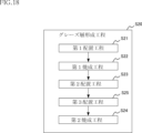
- FIG. 18 is a flowchart showing an example of another method for manufacturing the thermal print head shown in FIG. 12.
- FIG. 19 is an enlarged cross-sectional view showing a thermal print head according to a third embodiment of the present disclosure.
- FIG. 20 is an enlarged cross-sectional view showing a thermal print head according to a fourth embodiment of the present disclosure.
- FIG. 21 is a flowchart showing an example of a method for manufacturing the thermal print head shown in FIG. 20.
- FIG. 22 is a cross-sectional view showing one step of an example of a method for manufacturing the thermal print head shown in FIG. 20.
- FIG. 23 is a cross-sectional view showing one step of an example of a method for manufacturing the thermal print head shown in FIG. 20.
- FIG. 24 is a cross-sectional view showing one step in an example of a method for manufacturing the thermal print head shown in FIG. 20.
- FIG. 25 is an enlarged sectional view showing a thermal print head according to a first modification of the fourth embodiment.
- FIG. 26 is an enlarged sectional view showing a thermal print head according to a second modification of the fourth embodiment.
- a thing A is formed on a thing B and "a thing A is formed on a thing B” mean “a thing A is formed on a thing B” unless otherwise specified.
- "something A is placed on something B” and “something A is placed on something B” mean "something A is placed on something B” unless otherwise specified.
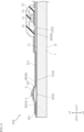
- First embodiment: 1 to 5 show a thermal print head A10 according to a first embodiment of the present disclosure.
- the thermal print head A10 of this embodiment includes a substrate 1, a glaze layer 2, an electrode layer 3, a resistor layer 4, a protective layer 5, a drive IC 71, a sealing resin 72, a wire 73, a connector 74, and a heat dissipation member 75. ing.
- the thermal print head A10 is incorporated into a thermal printer B1 that prints on a print medium 82 that is conveyed while being sandwiched between a platen roller 81 (see FIG. 2).
- the platen roller 81 is arranged to face the heat generating section 41, which will be described later, and presses the print medium 82 against the heat generating section 41 while conveying the print medium 82.
- print media 82 include thermal paper for creating barcode sheets and receipts.
- FIG. 1 is a plan view showing the thermal print head A10.
- FIG. 2 is a sectional view taken along line II-II in FIG.
- FIG. 3 is an enlarged plan view showing the thermal print head A10.
- FIG. 4 is a sectional view taken along line IV-IV in FIG. 3.
- FIG. 5 is an enlarged view of FIG. 4. Note that, for convenience of understanding, the protective layer 5 is omitted in FIGS. 1 and 3. Further, in these figures, the description will be made assuming that the longitudinal direction of the thermal print head A10 is the main scanning direction x, the lateral direction is the sub-scanning direction y, and the thickness direction is the thickness direction z. Regarding the sub-scanning direction y, the lower side of FIGS. 1 and 3 (the left side of FIG.
- FIGS. 1 and 3 are the upstream side y1 where the print medium 82 is sent
- the upper side of FIGS. 1 and 3 (the right side of FIG. 2) ) is the downstream side y2 from which the print medium 82 is discharged.
- the upper side in FIGS. 2 and 4 is defined as a first side z1
- the lower side in FIGS. 2 and 4 is defined as a second side z2.
- the left side in FIGS. 1 and 3 is defined as a first side x1
- the right side in FIGS. 1 and 3 is defined as a second side x2. The same applies to the following figures.
- the substrate 1 is made of ceramic such as AlN, Al 2 O 3 , or zirconia, and has a long rectangular plate shape that extends in the main scanning direction x when viewed in the thickness direction z, as shown in FIG. 1 .
- the thickness of the substrate 1 is not particularly limited, but is, for example, 0.6 mm or more and 1.0 mm or less.
- the substrate 1 has a main surface 11 and a back surface 12, as shown in FIG.
- the main surface 11 and the back surface 12 are surfaces facing opposite to each other in the thickness direction z.
- the main surface 11 faces the first side z1 in the thickness direction z.
- the back surface 12 faces the second side z2 in the thickness direction z.
- a glaze layer 2, an electrode layer 3, a resistor layer 4, and a protective layer 5 are arranged on the main surface 11 .
- a drive IC 71 is mounted on the main surface 11 .
- a heat radiating member 75 made of metal such as Al is arranged on the back surface 12 of the substrate 1.
- a connector 74 is arranged on the board 1. The connector 74 is connected to the connector of the thermal printer B1 when the thermal print head A10 is installed in the thermal printer B1.
- the materials and dimensions of the substrate 1 and the heat radiation member 75 are not limited.
- the thermal print head A10 may include a wiring board on the heat dissipation member 75 separately from the board 1, and the drive IC 71 and the connector 74 may be arranged on the wiring board.
- the glaze layer 2 is arranged on the main surface 11 of the substrate 1, and is made of a glass material such as amorphous glass.
- the glaze layer 2 is formed by disposing a glass paste and then firing it.
- the entire main surface 11 of the substrate 1 is covered with the glaze layer 2.
- the glaze layer 2 may have a configuration in which it does not cover a part of the main surface 11.
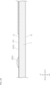
- the glaze layer 2 includes a first glaze layer 21, a second glaze layer 22, and a die bonding glaze 24.
- the first glaze layer 21 is arranged in contact with the main surface 11 of the substrate 1, and in this embodiment, it is arranged over the entire main surface 11.
- the first glaze layer 21 has a main surface 211 .
- the main surface 211 is a surface facing the first side z1 in the thickness direction z, and is flat over the entire surface.
- the first glaze layer 21 is provided to eliminate unevenness on the main surface 11 of the substrate 1 and to facilitate lamination of the electrode layer 3.
- the thickness of the first glaze layer 21 (dimension in the thickness direction z) is, for example, about 10 to 20 ⁇ m. Note that the thickness of the first glaze layer 21 is not limited.
- the softening point T1 of the first glaze material, which is the glass material of the first glaze layer 21, is, for example, about 1200 to 1300°C.
- the first glaze layer 21 is formed by disposing a glass paste on the main surface 11 of the substrate 1 by screen printing, for example, and then firing it. Note that the method for forming the first glaze layer 21 is not limited.
- the second glaze layer 22 is placed in contact with the main surface 211 of the first glaze layer 21.
- the second glaze layer 22 extends in the main scanning direction x and is strip-shaped when viewed in the thickness direction z.
- the second glaze layer 22 is disposed on the downstream side y2 of the main surface 211 of the first glaze layer 21 in the sub-scanning direction y.
- the second glaze layer 22 includes a main surface 221 .
- the main surface 221 is a surface facing the first side z1 in the thickness direction z, and is curved over substantially the entire surface.
- the shape of the cross section of the second glaze layer 22 perpendicular to the main scanning direction x is a shape that bulges toward the first side z1 in the thickness direction z.
- the second glaze layer 22 is provided to make it easier to press the heat generating portion 41 of the resistor layer 4 against the print medium 82 or the like. Further, the second glaze layer 22 has a function as a heat storage layer that accumulates the heat generated by the heat generating section 41.
- the thickness of the second glaze layer 22 (dimension in the thickness direction z) is, for example, about 100 to 200 ⁇ m. Note that the thickness of the second glaze layer 22 is not limited.
- the softening point T2 of the second glaze material which is the glass material of the second glaze layer 22, is lower than the softening point T1 of the first glaze material, for example, about 850 to 1000°C. Note that the softening point T2 is not limited.
- the second glaze layer 22 is formed by disposing a glass paste using a dispenser on the main surface 211 of the first glaze layer 21 formed by firing, and then firing it.
- the discharge port of the dispenser is a slit nozzle, and the long side dimension of the slit (dimension in the sub-scanning direction y when arranging the glass paste) depends on the width dimension (dimension in the sub-scanning direction y) of the second glaze layer 22 to be arranged. is set.
- the discharge amount of the dispenser can be adjusted. is set. Further, by adjusting the discharge pressure and moving speed of the dispenser, fine adjustment of the thickness dimension of the second glaze layer 22 is performed.
- the dispenser can adjust the dimensions of the glass paste to be placed by adjusting the dimensions of the slit, the discharge pressure, the moving speed, etc., and it is possible to arrange the glass paste at a thickness dimension that is difficult to arrange with screen printing. is possible.
- the die bonding glaze 24 is disposed in contact with the main surface 211 of the first glaze layer 21, and is spaced apart from the second glaze layer 22 on the upstream side y1 in the sub-scanning direction y. It is a belt-like shape extending in the main scanning direction x, which is provided parallel (or substantially parallel) to the main scanning direction x.
- the die bonding glaze 24 supports a part of the electrode layer 3 and the drive IC 71.
- the thickness of the die bonding glaze 24 (dimension in the thickness direction z) is, for example, about 30 to 50 ⁇ m. Note that the thickness of the die bonding glaze 24 is not limited.
- the softening point of the glass material of the die bonding glaze 24 is lower than the softening point T1 of the glass material of the first glaze layer 21, for example, about 850°C.
- the die bonding glaze 24 is formed by disposing a glass paste, for example, by screen printing, on the main surface 211 of the first glaze layer 21 formed by firing, and then firing this. Note that the method for forming the die bonding glaze 24 is not limited. Further, the glaze layer 2 does not need to include the die bonding glaze 24.
- the electrode layer 3 is for configuring a path for supplying electricity to the resistor layer 4, and is formed of a conductive material.
- the electrode layer 3 is made of resinate Au to which, for example, rhodium, vanadium, bismuth, silicon, or the like is added as an additive element.
- the electrode layer 3 is formed by printing a thick film of resinate Au paste and then firing it.
- the electrode layer 3 may be constructed by laminating a plurality of Au layers.
- the thickness of the electrode layer 3 is, for example, 0.3 ⁇ m or more and 1.5 ⁇ m or less. Note that the material, formation method, and thickness of the electrode layer 3 are not limited.
- the electrode layer 3 is arranged on the glaze layer 2. As shown in FIG.
- the electrode layer 3 includes a common electrode 33 and a plurality of individual electrodes 36. Note that, for convenience of understanding, the common electrode 33 and the individual electrodes 36 are hatched in FIG. Similarly, an Ag layer 351 to be described later is also hatched, and the resistor layer 4 is dotted.
- the common electrode 33 has a plurality of common electrode strip portions 34 and connecting portions 35.
- the connecting portion 35 is disposed near the downstream end y2 of the substrate 1 in the sub-scanning direction y, and has a band shape extending in the main-scanning direction x.
- the plurality of common electrode strips 34 each extend from the connecting portion 35 in the sub-scanning direction y, and are arranged at equal pitches and spaced apart from each other in the main-scanning direction x.
- an Ag layer 351 is laminated on the connecting portion 35.
- the Ag layer 351 is for reducing the resistance value of the connecting portion 35.
- the thickness of the Ag layer 351 is, for example, 2 ⁇ m or more and 10 ⁇ m or less.
- the plurality of individual electrodes 36 are for partially supplying current to the resistor layer 4, and are portions having opposite polarity to the common electrode 33.
- the individual electrodes 36 extend from the resistor layer 4 toward the drive IC 71 .
- the plurality of individual electrodes 36 are arranged in the main scanning direction x, and each has an individual electrode strip portion 38, a connecting portion 37, and a bonding portion 39.
- Each individual electrode strip 38 is a strip extending in the sub-scanning direction y, and is arranged between any two adjacent common electrode strips 34 of the common electrode 33.
- the distance between the individual electrode strip portions 38 of the adjacent individual electrodes 36 and the common electrode strip portion 34 of the common electrode 33 is, for example, 40 ⁇ m or less.
- the center-to-center distance between the individual electrode strip portions 38 of adjacent individual electrodes 36 and the common electrode strip portion 34 of the common electrode 33 is, for example, 20 ⁇ m or more and 100 ⁇ m or less.
- the connecting portion 37 is a portion extending from the individual electrode strip portion 38 toward the drive IC 71.
- the connecting portion 37 has a parallel portion 371 and an oblique portion 372.
- One end of the parallel portion 371 is connected to the bonding portion 39 and extends along the sub-scanning direction y.
- the oblique portion 372 is inclined with respect to the sub-scanning direction y.
- the oblique portion 372 is sandwiched between the parallel portion 371 and the individual electrode strip portion 38 in the sub-scanning direction y. Further, the plurality of individual electrodes 36 are integrated into the drive IC 71.
- the bonding part 39 is arranged at the upstream y1 end of the individual electrode 36 in the sub-scanning direction y, and is connected to the parallel part 371.
- a wire 73 for electrically connecting the individual electrode 36 and the drive IC 71 is bonded to the bonding portion 39 .
- the plurality of bonding parts 39 include a first bonding part 39A and a second bonding part 39B.
- the width (dimension in the main scanning direction x) of the parallel portion 371 sandwiched between two adjacent first bonding portions 39A is, for example, 20 ⁇ m or more and 30 ⁇ m or less.
- the second bonding portion 39B is located on the side farther away from the resistor layer 4 (upstream side y1) than the first bonding portion 39A in the sub-scanning direction y.
- the second bonding portion 39B is connected to a parallel portion 371 sandwiched between two adjacent first bonding portions 39A.
- each part of the electrode layer 3 are not particularly limited, and can have various configurations. Moreover, the material of each part of the electrode layer 3 is not limited either.
- the resistor layer 4 is made of, for example, ruthenium oxide, which has a higher resistivity than the material forming the electrode layer 3.
- the resistor layer 4 is disposed on the second glaze layer 22 and is formed in a band shape extending in the main scanning direction x.
- the resistor layer 4 is formed by printing a thick film of paste such as ruthenium oxide and then firing the paste.
- the resistor layer 4 intersects with and is in contact with the plurality of common electrode strips 34 of the common electrode 33 and the individual electrode strips 38 of the plurality of individual electrodes 36 .
- the resistor layer 4 is arranged on the opposite side of the substrate 1 (the first side z1 in the thickness direction z) with respect to the plurality of common electrode strips 34 of the common electrode 33 and the individual electrode strips 38 of the plurality of individual electrodes 36. ) are laminated. A portion of the resistor layer 4 sandwiched between each common electrode strip portion 34 and each individual electrode strip portion 38 serves as a heat generating portion 41 that generates heat when partially energized by the electrode layer 3 .
- the plurality of heat generating parts 41 are arranged in the second glaze layer 22 and arranged along the main scanning direction x. As shown in FIG. 2, in the thermal printer B1, the plurality of heat generating parts 41 are opposed to the platen roller 81.
- Print dots are formed by the heat generated by the heat generating section 41.
- the thickness of the resistor layer 4 is, for example, 1 ⁇ m or more and 10 ⁇ m or less, preferably 3 ⁇ m or more and 10 ⁇ m or less. Note that the material and thickness of the resistor layer 4 are not limited.
- the protective layer 5 is for protecting the electrode layer 3 and the resistor layer 4, and covers almost the entirety of the electrode layer 3 and the resistor layer 4. However, the protective layer 5 exposes a region including the bonding portions 39 of the plurality of individual electrodes 36.
- the protective layer 5 is made of a glass material such as amorphous glass.
- the protective layer 5 is formed by printing a thick film of glass paste and then firing it.
- the thickness of the protective layer 5 is, for example, 0.5 ⁇ m or more and 10 ⁇ m or less. Note that the material, formation method, and thickness of the protective layer 5 are not limited.
- the thermal print head A10 may further include a second protective layer that covers a portion of the protective layer 5.
- the drive IC 71 functions to partially generate heat in the resistor layer 4 by selectively energizing the plurality of individual electrodes 36.
- a plurality of drive ICs 71 are arranged on the die bonding glaze 24.
- the drive IC 71 is provided with a plurality of pads.
- the pads of the drive IC 71 and the plurality of individual electrodes 36 are connected via a plurality of wires 73 bonded to each pad.
- the wire 73 is made of Au, for example.
- the drive IC 71 and the wires 73 are covered with a sealing resin 72.
- the sealing resin 72 is made of, for example, a black insulating soft resin.
- the drive IC 71 and the connector 74 are connected via the wire 73 and the wiring on the board 1.
- FIG. 6 is a flowchart illustrating an example of a method for manufacturing the thermal print head A10.
- 7 to 11 are each a cross-sectional view showing one step of an example of a method for manufacturing the thermal print head A10, and correspond to the cross section shown in FIG. 4.
- the main scanning direction x, sub-scanning direction y, and thickness direction z shown in FIGS. 6 to 11 indicate the same directions as in FIGS. 1 to 5.
- the manufacturing method of the thermal print head A10 includes a substrate preparation step S10, a glaze layer forming step S20, an electrode layer forming step S30, a resistor layer forming step S40, a protective layer forming step S50, and a drive IC mounting and sealing step. It includes a stopping step S60 and an attaching step S70.
- a substrate 1 made of, for example, AlN, Al 2 O 3 or zirconia is prepared (substrate preparation step S10).
- the substrate 1 has a main surface 11 and a back surface 12 facing oppositely to each other in the thickness direction z.
- the main surface 11 faces the first side z1 in the thickness direction z.
- the back surface 12 faces the second side z2 in the thickness direction z.
- the glaze layer 2 is formed on the substrate 1, as shown in FIGS. 7 to 10 (glaze layer forming step S20).
- a glass paste of the first glaze material is placed on the entire main surface 11 of the substrate 1 by screen printing (first placement step S21).
- first glaze layer 21 is formed on the main surface 11, as shown in FIG. 7 (first firing step S22).
- the main surface 211 of the first glaze layer 21 is flat over the entire surface.
- a glass paste is placed at a predetermined position on the main surface 211 of the first glaze layer 21 by screen printing and fired, thereby forming a die bonding glaze 24 on the main surface 211, as shown in FIG. Ru.
- a glass paste 22A of the second glaze material is arranged in a belt shape extending in the main scanning direction x at a predetermined position on the main surface 211 of the first glaze layer 21 using a dispenser (second arrangement).
- a dispenser second arrangement
- the glass paste 22A is disposed with a larger thickness than when disposed by screen printing.
- the second glaze material is placed on the main surface 211 of the first glaze layer 21. Due to the coffee ring effect during drying, the second glaze material has a concave portion extending in the main scanning direction x in the central portion when viewed in the thickness direction z.
- the second glaze layer 22 is formed on the main surface 211 of the first glaze layer 21, as shown in FIG. 10 (second firing step S24).
- the second glaze layer 22 has a curved shape in which the main surface 221 protrudes toward the first side z1 in the thickness direction z due to the surface tension of the softened second glaze material. Therefore, as shown in FIG. 10, the cross section of the second glaze layer 22 perpendicular to the main scanning direction x has a shape that bulges toward the first side z1 in the thickness direction z.
- the firing temperature in the second firing step S24 to a temperature between the softening points T1 and T2 only the second glaze material can be fired without softening the first glaze layer 21.
- the glaze layer 2 is formed on the substrate 1.
- a metal film is formed by printing a thick film of resinate Au paste and then firing it.
- the metal film is patterned using, for example, etching.
- the electrode layer 3 is formed on the glaze layer 2 (electrode layer forming step S30).
- a thick film of paste containing Ag is printed on a predetermined area on the connecting portion 35 of the electrode layer 3, and then this is fired.
- an Ag layer 351 is formed as shown in FIG. 11.
- a resistor paste containing a resistor such as ruthenium oxide is printed as a thick film, and this is fired.
- the resistor layer 4 is formed (resistor layer forming step S40).
- the protective layer 5 is formed by, for example, printing a thick film of glass paste and baking it (protective layer forming step S50).
- the drive IC 71 is mounted, the wires 73 are bonded, and the sealing resin 72 is formed (drive IC mounting and sealing step S60).
- the connector 74 is attached to the substrate 1, the substrate 1 is attached to the heat dissipation member 75, etc. (attachment step S70).
- the thermal print head A10 shown in FIGS. 1 to 5 is manufactured.
- the manufacturing method described above is an example and is not limited thereto.
- the glaze layer 2 of the thermal print head A10 includes a second glaze layer 22.
- the second glaze layer 22 is formed by disposing a glass paste 22A using a dispenser on the main surface 211 of the first glaze layer 21 disposed on the main surface 11 of the substrate 1, and then firing it. Therefore, the thickness of the second glaze layer 22 can be increased compared to a case where a glass paste placed by screen printing is fired. Therefore, in the thermal print head A10, the heat generating section 41 can be easily pressed against the print medium 82, etc., and the heat generated by the heat generating section 41 can be efficiently transmitted to the print medium 82. Further, since the second glaze layer 22 can accumulate more heat generated by the heat generating section 41, the thermal print head A10 can suppress the amount of heat that must be generated by the heat generating section 41. Therefore, the thermal print head A10 can suppress power consumption and further improve printing efficiency.
- the second glaze layer 22 is formed on the main surface 211 of the first glaze layer 21 formed by firing in the first firing step S22. Therefore, in the thermal print head A10, the second glaze layer 22 is first formed on the substrate 1, and then the first glaze layer 21 is formed adjacent to the second glaze layer 22. can be arranged at a position away from the main surface 11 of the substrate 1 in the thickness direction z. This makes it easier for the thermal print head A10 to press the heat generating section 41 against the print medium 82 or the like.
- the softening point T2 of the second glaze material is lower than the softening point T1 of the first glaze material. Therefore, in the second firing step S24, by setting the firing temperature to a temperature between the softening points T1 and T2, only the second glaze material can be fired without softening the first glaze layer 21.
- FIG. 12 to 17 are diagrams for explaining a thermal print head A20 according to a second embodiment of the present disclosure.
- FIG. 12 is an enlarged sectional view showing the thermal print head A20, and corresponds to FIG. 5.
- FIG. 13 is a flowchart illustrating an example of a method for manufacturing the thermal print head A20, and corresponds to FIG. 6.
- 14 to 17 are cross-sectional views showing one step of an example of a method for manufacturing the thermal print head A20, and correspond to FIGS. 9 and 10.
- the thermal print head A20 of this embodiment differs from the embodiments described above in that the glaze layer 2 further includes a third glaze layer 23.
- the configuration and operation of other parts of this embodiment are similar to those of the first embodiment.
- each part of the said 1st Embodiment may be combined arbitrarily.
- the second glaze layer 22 includes regions 22a, 22b, and 22c, as shown in FIG. 12.
- the regions 22a, 22b, and 22c each have the same shape as the second glaze layer 22 according to the first embodiment, and extend in the main scanning direction x.
- the regions 22a, 22b, and 22c are spaced apart from each other in the sub-scanning direction y.
- the glaze layer 2 further includes a third glaze layer 23.
- the third glaze layer 23 is interposed between the second glaze layer 22 and the plurality of heat generating parts 41, and covers the entire second glaze layer 22 (regions 22a, 22b, 22c). Note that the third glaze layer 23 does not need to cover a part of the second glaze layer 22.
- the third glaze layer 23 extends in the main scanning direction x and is strip-shaped when viewed in the thickness direction z.
- the softening point T3 of the third glaze material which is the glass material of the third glaze layer 23, is lower than the softening point T2 of the second glaze material, for example, about 850°C.
- the glaze layer forming step S20 further includes a third arrangement step S25 and a third firing step S26.
- the steps (S10, S30 to S70) other than the glaze layer forming step S20 are the same as in the first embodiment.
- the first arrangement step S21, the first firing step S22, and the step of forming the die bonding glaze 24 are the same as in the first embodiment (see FIGS. 7 and 8).
- the second arrangement step S23 by repeating the arrangement of the glass paste 22A by the dispenser three times, as shown in FIG. 14, three strip-shaped glass pastes 22A extending in the main scanning direction x are arranged at a distance from each other.
- the second glaze layer 22 (regions 22a, 22b, 22c) is formed on the main surface 211 of the first glaze layer 21, as shown in FIG. is formed (second firing step S24).
- glass paste 23A of the third glaze material is placed by a dispenser to cover the entire second glaze layer 22 (regions 22a, 22b, 22c) (third placement step S25).
- the glass paste 23A is arranged in a band shape extending in the main scanning direction x.
- the surface of the glass paste 23A has irregularities formed in accordance with the shapes of the regions 22a, 22b, and 22c.
- the third glaze material is placed to cover the second glaze layer 22 (regions 22a, 22b, 22c).
- the third glaze layer 23 covering the second glaze layer 22 is formed as shown in FIG. 17 (third firing step S26).
- the third glaze layer 23 has a curved shape in which the main surface 231 protrudes toward the first side z1 in the thickness direction z due to the surface tension of the softened third glaze material. Furthermore, by setting the firing temperature in the third firing step S26 to a temperature between the softening points T2 and T3, only the third glaze material can be fired without softening the second glaze layer 22.
- the thermal print head A20 has the same effects as the thermal print head A10.
- the glaze layer 2 of the thermal print head A20 includes a second glaze layer 22 (regions 22a, 22b, 22c) and a third glaze layer 23.
- the combination of the second glaze layer 22 (regions 22a, 22b, 22c) and the third glaze layer 23 may be referred to as a "partial glaze”.
- the partial glaze is obtained by further covering the second glaze layer 22 (regions 22a, 22b, 22c) with a third glaze layer 23, and has a larger thickness than the second glaze layer 22. Therefore, compared to the thermal print head A10, the thermal print head A20 can further suppress power consumption and further improve printing efficiency.
- the second glaze layer 22 includes regions 22a, 22b, and 22c spaced apart in the sub-scanning direction y. Therefore, the partial glaze can have a larger dimension in the sub-scanning direction y than the second glaze layer 22 according to the first embodiment. As a result, the volume of the partial glaze can be increased, so that more heat generated by the heat generating portion 41 can be accumulated. Therefore, the thermal print head A20 can further improve printing efficiency.
- the third glaze layer 23 is formed to cover the second glaze layer 22 formed by firing in the second firing step S24. Therefore, compared to the thermal print head A10, the thermal print head A20 can dispose the heat generating part 41 at a position farther away from the main surface 11 of the substrate 1 in the thickness direction z. This makes it easier for the thermal print head A20 to press the heat generating portion 41 against the print medium 82 or the like.
- the softening point T3 of the third glaze material is lower than the softening point T2 of the second glaze material. Therefore, in the third firing step S26, by setting the firing temperature to a temperature between the softening points T2 and T3, only the third glaze material can be fired without softening the second glaze layer 22.
- the second glaze layer 22 includes three regions 22a, 22b, and 22c, but the present invention is not limited to this.
- the second glaze layer 22 may include two regions, or may include four or more regions. The larger the number of regions included in the second glaze layer 22, the larger the dimension of the partial glaze in the sub-scanning direction y.
- the second glaze layer 22 (regions 22a, 22b, 22c) is formed in the second firing step S24, and then the third glaze material is placed in the third placement step S25, but this is not limited to this. I can't do it.
- the third glaze material is first arranged in the third arrangement step S25, and the second glaze material and the third glaze material are combined in the second firing step S24. It may also be fired.
- the softening point T3 of the third glaze material may be the same (or substantially the same) as the softening point T2 of the second glaze material.
- FIG. 19 is a diagram for explaining a thermal print head A30 according to a third embodiment of the present disclosure.
- FIG. 19 is an enlarged cross-sectional view showing the thermal print head A30, and corresponds to FIG. 5.
- the thermal print head A30 of this embodiment differs from the above-described second embodiment in that the second glaze layer 22 consists of one region.
- the configuration and operation of other parts of this embodiment are similar to those of the second embodiment. Note that each part of the first and second embodiments described above may be combined arbitrarily.
- the second glaze layer 22 according to the present embodiment does not include a plurality of regions, and has the same configuration as the second glaze layer 22 according to the first embodiment.
- the glaze layer 2 includes the third glaze layer 23, similar to the second embodiment.
- the third glaze layer 23 has the same configuration as the third glaze layer 23 according to the second embodiment.
- the method for manufacturing the thermal print head A30 is the same as the method for manufacturing the thermal print head A20, except that the glass paste 22A is placed only once in the second placement step S23.
- the thermal print head A30 has the same effects as the thermal print head A10.
- the glaze layer 2 of the thermal print head A30 includes a partial glaze (a combination of the second glaze layer 22 and the third glaze layer 23).
- the partial glaze is obtained by further covering the second glaze layer 22 with a third glaze layer 23, and has a larger thickness than the second glaze layer 22. Therefore, compared to the thermal print head A10, the thermal print head A30 can further suppress power consumption and further improve printing efficiency.
- the third glaze layer 23 is formed to cover the second glaze layer 22 formed by firing in the second firing step S24. Therefore, compared to the thermal print head A10, the thermal print head A30 can dispose the heat generating part 41 at a position farther away from the main surface 11 of the substrate 1 in the thickness direction z. This makes it easier for the thermal print head A30 to press the heat generating section 41 against the print medium 82 or the like.
- the softening point T3 of the third glaze material is lower than the softening point T2 of the second glaze material. Therefore, in the third firing step S26, by setting the firing temperature to a temperature between the softening points T2 and T3, only the third glaze material can be fired without softening the second glaze layer 22.
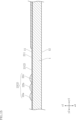
- FIG. 20 to 24 are diagrams for explaining a thermal print head A40 according to a fourth embodiment of the present disclosure.
- FIG. 20 is an enlarged sectional view showing the thermal print head A40, and is a further enlarged view of the diagram corresponding to FIG.
- FIG. 21 is a flowchart illustrating an example of a method for manufacturing the thermal print head A40, and corresponds to FIG. 6. In addition, in FIG. 21, only the glaze layer forming step S20 is described, and the description of other steps is omitted.
- 22 to 24 are cross-sectional views showing one step of an example of a method for manufacturing the thermal print head A40.
- the thermal print head A40 of this embodiment differs from the first embodiment described above in that a recess is formed in the first glaze layer 21 and the second glaze layer 22 is disposed in the recess.
- the configuration and operation of other parts of this embodiment are similar to those of the first embodiment. Note that each part of the first to third embodiments described above may be combined arbitrarily.
- the first glaze layer 21 includes a recess 212.
- the recess 212 is a groove recessed from the main surface 211 toward the second side z2 in the thickness direction z, and extends linearly in the main scanning direction x.
- the recess 212 has an elongated rectangular shape that extends in the main scanning direction x when viewed in the thickness direction z.
- the depth dimension (dimension in the thickness direction z) of the recess 212 is not limited.
- the recess 212 is formed, for example, by wet blasting. Wet blasting is a processing technology that processes a target object by accelerating a slurry made by mixing abrasive material and water (sometimes containing chemicals) with compressed air and spraying it toward the target object. .
- the recesses 212 are formed by forming a mask layer on the main surface 211 and performing processing by wet blasting on the region on the main surface 211 where the mask layer is not formed.
- the method for forming the recess 212 is not limited.
- the recess 212 may be formed, for example, by shot blasting other than wet blasting, by etching, or by cutting with a dicing blade, laser, or the like.
- the recess 212 includes two recess edges 212a. Each recess edge 212a is a boundary between the recess 212 and the main surface 211, and extends in the main scanning direction x.
- the inclination angle ⁇ of the side surface 212b of the recess 212 with respect to the main surface 211 is approximately a right angle. Note that the inclination angle ⁇ is not limited to a substantially right angle.
- the second glaze layer 22 is arranged inside the recess 212 when viewed in the thickness direction z.
- the second glaze layer 22 is formed by placing glass paste in the recess 212 and firing it. Although the glass paste is fluid, when placed in the recess 212, surface tension prevents it from exceeding the recess edge 212a. Also, during firing, the glass paste is fluidized by heating, but surface tension prevents it from exceeding the edge 212a of the recess.
- the recess 212 only needs to have a recess edge 212a for preventing the glass paste from flowing and spreading onto the main surface 211. Therefore, the depth dimension of the recess 212 may be relatively small. Further, it is desirable that the inclination angle ⁇ is relatively large.
- the glaze edge 222 which is the edge of the second glaze layer 22 in the sub-scanning direction y, coincides with the recess edge 212a of the recess 212. More specifically, the glaze edge 222 on the upstream side y1 in the sub-scanning direction y and the recess edge 212a on the upstream side y1 in the sub-scanning direction y coincide with the glaze edge 222 on the downstream side y2 in the sub-scanning direction y.
- the concave portion edge 212a on the downstream side y2 in the sub-scanning direction y coincides with the concave portion edge 212a.
- the second glaze layer 22 is formed with a formation region defined by the recess 212 .
- the method for manufacturing the thermal print head A40 includes a recess forming step S27 added between the first firing step S22 and the second arrangement step S23.
- the steps (S10, S30 to S70) other than the glaze layer forming step S20 are the same as in the first embodiment.
- the first arrangement step S21, the first firing step S22, and the step of forming the die bonding glaze 24 are the same as in the first embodiment (see FIGS. 7 and 8).
- recesses 212 are formed in the first glaze layer 21 (recess formation step S27).
- a predetermined mask layer 99 (indicated by a two-dot chain line in FIG. 22) is formed on a part of the main surface 211 of the first glaze layer 21.
- the mask layer 99 is formed, for example, by patterning a resist using a photolithography technique.
- the mask layer 99 has an opening 99a that penetrates the mask layer 99 in the thickness direction z and extends in the main scanning direction x.
- wet blasting is performed to form a recess 212 that is recessed from the main surface 211 in the thickness direction z and extends in the main scanning direction x, as shown in FIG.
- the shape of the recess 212 when viewed in the thickness direction z corresponds to the opening 99a of the mask layer 99.
- the recess 212 includes a bottom surface 212c facing the first side z1 in the thickness direction z.
- the bottom surface 212c has irregularities formed by wet blasting. Thereafter, mask layer 99 is removed.
- a glass paste 22A of the second glaze material is placed in the recess 212 of the first glaze layer 21 using a dispenser.
- the placed glass paste 22A has fluidity, surface tension prevents it from exceeding the recess edge 212a.
- the method for disposing the glass paste 22A is not limited, and may be disposed by, for example, screen printing.
- the second glaze layer 22 is formed in the recess 212 of the first glaze layer 21, as shown in FIG.
- the glass paste 22A is fluidized by heating during firing, surface tension prevents it from exceeding the recess edge 212a.
- the second glaze layer 22 is formed in a state where the glaze edge 222 and the recess edge 212a are aligned with each other when viewed in the thickness direction z.
- the thermal print head A40 has the same effects as the thermal print head A10.
- the first glaze layer 21 includes a recess 212 that is recessed from the main surface 211 toward the second side z2 in the thickness direction z and extends in the main scanning direction x.
- the second glaze layer 22 is disposed inside the recess 212 when viewed in the thickness direction z.
- the second glaze layer 22 is formed by preventing the fluid glass paste 22A from exceeding the recess edge 212a of the recess 212 during the manufacturing process. Thereby, the second glaze layer 22 is formed in the formation region defined by the recess 212 without spreading on the main surface 211. Therefore, the thermal print head A40 can make each glaze edge 222 of the second glaze layer 22 linear. Furthermore, the thermal print head A40 can prevent the second glaze layer 22 from spreading on the main surface 211 and reducing the thickness dimension.
- the recess 212 is formed by wet blasting. Therefore, the recess 212 can be easily formed in a short time. Further, the recess 212 can be formed so that the inclination angle ⁇ is approximately a right angle.
- FIGS. 25 and 26 show a modification of the thermal print head A40 according to the fourth embodiment.
- the same or similar elements as in the above embodiment are given the same reference numerals as in the above embodiment, and redundant explanation will be omitted.
- FIG. 25 is a diagram for explaining a thermal print head A41 according to a first modification of the fourth embodiment.
- FIG. 25 is an enlarged sectional view showing the thermal print head A41, and corresponds to FIG. 20.
- the recess 212 according to this modification is composed of two grooves 213 lined up in the sub-scanning direction y.
- Each groove 213 is a groove recessed from the main surface 211 toward the second side z2 in the thickness direction z, and extends in the main scanning direction x.
- Each groove 213 has an elongated rectangular shape that extends in the main scanning direction x when viewed in the thickness direction z.
- Each groove 213 is formed, for example, by wet blasting. Note that the method of forming each groove 213 is not limited.
- Each groove 213 includes a recess edge 213a and a recess edge 213b.
- the recess edge 213a and the recess edge 213b are boundaries between each groove 213 and the main surface 211, and extend in the main scanning direction x.
- the recess edge 213a is an edge located on the opposite side of the other groove 213 in the sub-scanning direction y.
- the recess edge 213b is an edge located on the other groove 213 side in the sub-scanning direction y.
- the main surface 211 is divided into three parts by a recess 212 (two grooves 213). All three portions have an elongated rectangular shape that extends in the main scanning direction x.
- the main surface 211 includes a groove portion 211a.
- the inter-groove portion 211a is a portion between two grooves 213 among the three portions. In other words, the groove portion 211a is connected to the groove 213 via the recess edge 213b.
- the second glaze layer 22 is disposed on the groove portion 211a of the main surface 211 and in each groove 213 when viewed in the thickness direction z.
- the glass paste 22A which is the material of the second glaze layer 22, has fluidity, but when placed on the first glaze layer 21, surface tension prevents it from exceeding the recess edge 213a. Also, during firing, the glass paste 22A is fluidized by heating, but surface tension prevents it from exceeding the edge 213a of the recess. When viewed in the thickness direction z, the glaze edge 222 and the recess edge 213a match.
- the glaze edge 222 on the upstream side y1 in the sub-scanning direction y and the recess edge 213a of the groove 213 on the upstream side y1 in the sub-scanning direction y match, and the glaze edge 222 on the upstream side y1 in the sub-scanning direction y coincides with the glaze edge 213a on the downstream side y2 in the sub-scanning direction y.
- the edge 222 and the recess edge 213a of the groove 213 on the downstream side y2 in the sub-scanning direction y are aligned.
- the second glaze layer 22 is formed with a formation region defined by the recess edge 213 a of each groove 213 of the recess 212 .
- the first glaze layer 21 includes a recess 212 that is recessed from the main surface 211 toward the second side z2 in the thickness direction z and that is made up of two grooves 213 that extend in the main scanning direction x. ing. Further, the second glaze layer 22 is disposed on the groove portion 211a of the main surface 211 and in each groove 213 when viewed in the thickness direction z. The second glaze layer 22 is formed by preventing the fluid glass paste 22A from exceeding the recessed edge 213a of each groove 213 during the manufacturing process. Thereby, the second glaze layer 22 is formed in the formation region defined by the recess 212 without spreading on the main surface 211.
- each glaze edge 222 of the second glaze layer 22 can be made straight, and the thickness can be increased by spreading the second glaze layer 22 on the main surface 211. It is possible to suppress the size from becoming smaller.
- FIG. 26 is a diagram for explaining a thermal print head A42 according to a second modification of the fourth embodiment.
- FIG. 26 is an enlarged sectional view showing the thermal print head A42, and corresponds to FIG. 20.
- the formation region of the second glaze layer 22 is different from the first modification described above.
- the recess 212 consists of two grooves 213 aligned in the sub-scanning direction y.
- Each groove 213 includes a recess edge 213a and a recess edge 213b.
- the main surface 211 includes an inter-groove portion 211 a located between the two grooves 213 .
- the second glaze layer 22 is disposed on the groove portion 211a of the main surface 211 and is not disposed on the two grooves 213 when viewed in the thickness direction z. That is, the two grooves 213 are exposed from the second glaze layer 22.
- the glass paste 22A which is the material of the second glaze layer 22, has fluidity, but when placed on the first glaze layer 21, surface tension prevents it from exceeding the edge 213b of the recess. Also, during firing, the glass paste 22A is fluidized by heating, but surface tension prevents it from exceeding the edge 213b of the recess. When viewed in the thickness direction z, the glaze edge 222 and the recess edge 213b match.
- the glaze edge 222 on the upstream side y1 in the sub-scanning direction y and the recess edge 213b of the groove 213 on the upstream side y1 in the sub-scanning direction y match, and the glaze edge 222 on the upstream side y1 in the sub-scanning direction y coincides with the glaze edge 213b on the downstream side y2 in the sub-scanning direction y.
- the edge 222 and the recess edge 213b of the groove 213 on the downstream side y2 in the sub-scanning direction y are aligned.
- the second glaze layer 22 is formed with a formation region defined by the recess edge 213b of each groove 213 of the recess 212.
- the first glaze layer 21 includes a recess 212 consisting of two grooves 213.
- the second glaze layer 22 is disposed only on the groove portion 211a of the main surface 211 when viewed in the thickness direction z.
- the second glaze layer 22 is formed by preventing the fluid glass paste 22A from exceeding the recessed edge 213b of each groove 213 during the manufacturing process. Thereby, the second glaze layer 22 is formed in the formation region defined by the recess 212 without spreading on the main surface 211. Therefore, in the thermal print head A42, like the thermal print head A40, each glaze edge 222 of the second glaze layer 22 can be made straight, and the thickness can be increased by spreading the second glaze layer 22 on the main surface 211. It is possible to suppress the size from becoming smaller.
- thermal print head and its manufacturing method according to the present disclosure, and the thermal printer equipped with the thermal print head are not limited to the embodiments described above.
- the specific configuration of each part of the thermal print head and thermal printer according to the present disclosure, and the specific processing of each step of the method for manufacturing a thermal print head according to the present disclosure can be variously changed in design.
- the present disclosure includes the embodiments described in the appendix below.
- a substrate (1) having a substrate main surface (11) facing a first side (z1) in the thickness direction (z); a first glaze layer (21) disposed on the substrate main surface and having a first glaze main surface (211) facing the first side; a band-shaped second glaze layer (22) disposed in contact with the first glaze main surface and extending in the main scanning direction (x); a resistor layer (4) including a plurality of heat generating parts (41) arranged along the main scanning direction; Equipped with The plurality of heat generating parts are arranged in the second glaze layer, Thermal print head (A10).
- Appendix 2. the first glaze layer is disposed over the entire main surface of the substrate; The thermal print head described in Appendix 1.
- the second glaze layer includes a second glaze main surface (221) facing the first side, The first glazed main surface is flat compared to the second glazed main surface.
- the thermal print head according to appendix 1 or 2.
- Appendix 4 The second softening point (T2) of the second glaze layer is lower than the first softening point (T1) of the first glaze layer.
- the thermal print head according to any one of Supplementary Notes 1 to 3.
- Supplementary note 5 second and third embodiments, FIG. 12, FIG. 19. further comprising a belt-shaped third glaze layer (23) interposed between the second glaze layer and the plurality of heat generating parts and extending in the main scanning direction;
- the thermal print head according to any one of Supplementary Notes 1 to 4.
- the second glaze layer includes a plurality of regions (22a, 22b, 22c) spaced apart from each other in the sub-scanning direction.
- Appendix 7. The third softening point (T3) of the third glaze layer is lower than the second softening point of the second glaze layer.
- the thermal print head according to appendix 5 or 6. Appendix 7-1.
- the third softening point of the third glaze layer is the same (or approximately the same) as the second softening point of the second glaze layer.
- the substrate includes ceramics.
- the first glaze layer further includes a recess (212) recessed from the first glaze main surface in the thickness direction,
- the recess includes a recess edge (212a) that is a boundary with the first glaze main surface and extends in the main scanning direction, When viewed in the thickness direction, a glaze edge (222) of the second glaze layer and an edge of the recess are aligned;
- the thermal print head according to any one of appendices 1 to 8.
- the recess is a single groove extending in the main scanning direction, the second glaze layer is disposed inside the recess when viewed in the thickness direction;
- the recess includes two grooves (213) arranged in the sub-scanning direction,
- the second glaze layer is disposed in an inter-groove portion (211a) that is a region between the two grooves on the first glaze main surface and in the two grooves when viewed in the thickness direction.
- the recess includes two grooves aligned in the sub-scanning direction,
- the second glaze layer is disposed in an inter-groove portion that is a region between the two grooves on the first glaze main surface when viewed in the thickness direction, the two grooves are exposed from the second glaze layer,
- the recess includes a bottom surface (212c) facing the first side in the thickness direction, unevenness is formed on the bottom surface;
- the thermal print head according to any one of appendices 9 to 12.
- Appendix 14, Figure 2 The thermal print head according to any one of appendices 1 to 13, a platen roller (81) arranged to face the plurality of heat generating parts; It is equipped with Thermal printer (B1).
- the second glaze material arranged in the second arrangement step includes a plurality of regions (22A) spaced apart from each other in the sub-scanning direction (y), After the second arranging step, the method further includes a third arranging step (S25) of arranging a third glaze material (23A) in the form of a belt extending in the main scanning direction so as to cover the second glaze material.
- the third arrangement step is performed after the second firing step, After the third arrangement step, the method further includes a third firing step (S26) of firing the third glaze material.
- the second firing step is performed after the third arranging step, and the second glaze material and the third glaze material are fired.
- a first glaze formed by firing the first glaze material is recessed from the main surface in the thickness direction and extends in the main scanning direction. further comprising a recess forming step (S27) for forming a recess;
- S27 recess forming step for forming a recess
- the second glaze material is placed in the recess,
- the recess includes two grooves aligned in the sub-scanning direction,
- the second glaze is applied to an inter-groove portion, which is a region between the two grooves on the first glaze main surface, and to the two grooves, when viewed in the thickness direction. placing materials,
- the recess includes two grooves aligned in the sub-scanning direction, In the second arranging step, the second glaze material is arranged only in an inter-groove portion that is a region between the two grooves on the first glaze main surface when viewed in the thickness direction.
- the recess is formed by wet blasting.
- Appendix 25. the first glaze material is disposed over the entire main surface of the substrate;
Landscapes
- Electronic Switches (AREA)
Abstract
サーマルプリントヘッド(A10)において、厚さ方向の第1側を向く基板主面(11)を有する基板(1)と、前記基板主面(11)に配置され、かつ、前記第1側を向く第1グレーズ主面(211)を有する第1グレーズ層(21)と、前記第1グレーズ主面(211)に接して配置され、かつ、主走査方向に延びる帯状の第2グレーズ層(22)と、前記主走査方向に沿って配列された複数の発熱部を含む抵抗体層(4)と、を備えた。前記複数の発熱部は、前記第2グレーズ層(22)に配置されている。
Description
本開示は、サーマルプリントヘッドおよびその製造方法と、当該サーマルプリントヘッドを備えているサーマルプリンタに関する。
特許文献1には、従来のサーマルプリントヘッドの一例が開示されている。特許文献1に記載のサーマルプリントヘッドは、基板上にグレーズ層が形成されている。グレーズ層には、部分グレーズおよびガラス層が含まれている。部分グレーズは、発熱部を印刷媒体に押し当て易くし、また、発熱部からの熱を蓄積して、印字効率を向上させるために設けられている。ガラス層は、部分グレーズに隣接して部分グレーズの一部に重なって形成され、上面が平坦な形状である。部分グレーズは、基板の主面上にスクリーン印刷によりガラスペーストを配置し、焼成することで形成される。ガラス層は、部分グレーズを形成した基板上にガラスペーストを厚膜印刷し、焼成することで形成される。サーマルプリントヘッドにおいては、印字効率のさらなる向上が望まれている。
本開示は、従来より改良が施された半導体装置を提供することを一の課題とする。特に本開示は、上記した事情に鑑み、印字効率のさらなる向上が可能なサーマルプリントヘッドを提供することをその一の課題とする。
本開示の一の側面によって提供されるサーマルプリントヘッドは、厚さ方向の第1側を向く基板主面を有する基板と、前記基板主面に配置され、かつ、前記第1側を向く第1グレーズ主面を有する第1グレーズ層と、前記第1グレーズ主面に接して配置され、かつ、主走査方向に延びる帯状の第2グレーズ層と、前記主走査方向に沿って配列された複数の発熱部を含む抵抗体層と、を備える。前記複数の発熱部は、前記第2グレーズ層に配置されている。
本開示の他の側面によって提供されるサーマルプリントヘッドの製造方法は、厚さ方向の第1側を向く基板主面を有する基板を準備する基板準備工程と、前記基板主面上に第1グレーズ材料を配置する第1配置工程と、前記第1グレーズ材料上に、ディスペンサにより主走査方向に延びる帯状の第2グレーズ材料を配置する第2配置工程と、を備えている。
上記構成によれば、印字効率のさらなる向上が可能である。
本開示のその他の特徴および利点は、添付図面を参照して以下に行う詳細な説明によって、より明らかとなろう。
以下、本開示の好ましい実施の形態につき、図面を参照して具体的に説明する。
本開示において、「ある物Aがある物Bに形成されている」および「ある物Aがある物B上に形成されている」とは、特段の断りのない限り、「ある物Aがある物Bに直接形成されていること」、および、「ある物Aとある物Bとの間に他の物を介在させつつ、ある物Aがある物Bに形成されていること」を含む。同様に、「ある物Aがある物Bに配置されている」および「ある物Aがある物B上に配置されている」とは、特段の断りのない限り、「ある物Aがある物Bに直接配置されていること」、および、「ある物Aとある物Bとの間に他の物を介在させつつ、ある物Aがある物Bに配置されていること」を含む。同様に、「ある物Aがある物B上に位置している」とは、特段の断りのない限り、「ある物Aがある物Bに接して、ある物Aがある物B上に位置していること」、および、「ある物Aとある物Bとの間に他の物が介在しつつ、ある物Aがある物B上に位置していること」を含む。また、「ある物Aがある物Bにある方向に見て重なる」とは、特段の断りのない限り、「ある物Aがある物Bのすべてに重なること」、および、「ある物Aがある物Bの一部に重なること」を含む。
第1実施形態:
図1~図5は、本開示の第1実施形態に係るサーマルプリントヘッドA10を示している。本実施形態のサーマルプリントヘッドA10は、基板1、グレーズ層2、電極層3、抵抗体層4、保護層5、駆動IC71、封止樹脂72、ワイヤ73、コネクタ74、および放熱部材75を備えている。サーマルプリントヘッドA10は、プラテンローラ81との間に挟まれて搬送される印刷媒体82に印刷を施すサーマルプリンタB1に組み込まれるものである(図2参照)。プラテンローラ81は、後述する発熱部41に対向して配置されており、印刷媒体82を搬送しつつ、印刷媒体82を発熱部41に押圧する。このような印刷媒体82としては、たとえばバーコードシートやレシートを作成するための感熱紙が挙げられる。
図1~図5は、本開示の第1実施形態に係るサーマルプリントヘッドA10を示している。本実施形態のサーマルプリントヘッドA10は、基板1、グレーズ層2、電極層3、抵抗体層4、保護層5、駆動IC71、封止樹脂72、ワイヤ73、コネクタ74、および放熱部材75を備えている。サーマルプリントヘッドA10は、プラテンローラ81との間に挟まれて搬送される印刷媒体82に印刷を施すサーマルプリンタB1に組み込まれるものである(図2参照)。プラテンローラ81は、後述する発熱部41に対向して配置されており、印刷媒体82を搬送しつつ、印刷媒体82を発熱部41に押圧する。このような印刷媒体82としては、たとえばバーコードシートやレシートを作成するための感熱紙が挙げられる。
図1は、サーマルプリントヘッドA10を示す平面図である。図2は、図1のII-II線に沿う断面図である。図3は、サーマルプリントヘッドA10を示す拡大平面図である。図4は、図3のIV-IV線に沿う断面図である。図5は、図4の拡大図である。なお、理解の便宜上、図1および図3においては、保護層5を省略している。また、これらの図において、サーマルプリントヘッドA10の長手方向を主走査方向xとし、短手方向を副走査方向yとし、厚さ方向を厚さ方向zとして説明する。また、副走査方向yについては、図1および図3の下方(図2の左方)を印刷媒体82が送られてくる上流側y1とし、図1および図3の上方(図2の右方)を印刷媒体82が排出される下流側y2とする。また、厚さ方向zについては、図2および図4の上方を第1側z1とし、図2および図4の下方を第2側z2とする。また、主走査方向xについては、図1および図3の左方を第1側x1とし、図1および図3の右方を第2側x2とする。以下の図においても同様である。
基板1は、たとえばAlN、Al2O3、ジルコニアなどのセラミックからなり、図1に示すように、厚さ方向zに視て、主走査方向xに長く延びる長矩形状の板状である。基板1の厚さは、特に限定されないが、たとえば0.6mm以上1.0mm以下である。基板1は、図4に示すように、主面11および裏面12を有している。主面11および裏面12は、厚さ方向zにおいて互いに反対側を向く面である。主面11は、厚さ方向zの第1側z1を向いている。裏面12は、厚さ方向zの第2側z2を向いている。基板1の主面11には、グレーズ層2、電極層3、抵抗体層4、および保護層5が配置されている。また、主面11には、駆動IC71が搭載されている。図2に示すように、基板1の裏面12には、たとえばAlなどの金属からなる放熱部材75が配置されている。また、図1および図2に示すように、基板1には、コネクタ74が配置されている。コネクタ74は、サーマルプリントヘッドA10をサーマルプリンタB1に組み込む際に、サーマルプリンタB1のコネクタと接続される。なお、基板1および放熱部材75の材料および寸法は限定されない。また、サーマルプリントヘッドA10は、基板1とは別に放熱部材75上に配線基板を備え、配線基板に駆動IC71およびコネクタ74が配置されてもよい。
グレーズ層2は、基板1の主面11上に配置されており、たとえば非晶質ガラスなどのガラス材料からなる。グレーズ層2は、ガラスペーストを配置したのちに、これを焼成することにより形成されている。本実施形態においては、基板1の主面11の全面がグレーズ層2によって覆われている。なお、グレーズ層2は、主面11の一部を覆わない構成であってもよい。本実施形態においては、図4および図5に示すように、グレーズ層2は、第1グレーズ層21、第2グレーズ層22、およびダイボンディンググレーズ24を含んでいる。
第1グレーズ層21は、基板1の主面11に接して配置されており、本実施形態では、主面11の全面に配置されている。第1グレーズ層21は、主面211を備えている。主面211は、厚さ方向zの第1側z1を向く面であり、全面にわたって平坦である。第1グレーズ層21は、基板1の主面11の凹凸をなくして電極層3を積層しやすくするために設けられている。第1グレーズ層21の厚さ(厚さ方向zの寸法)は、たとえば10~20μm程度である。なお、第1グレーズ層21の厚さは限定されない。第1グレーズ層21のガラス材料である第1グレーズ材料の軟化点T1は、たとえば1200~1300℃程度である。なお、軟化点T1は限定されない。第1グレーズ層21は、たとえばスクリーン印刷によりガラスペーストを基板1の主面11に配置したのちに、これを焼成することで形成される。なお、第1グレーズ層21の形成方法は限定されない。
第2グレーズ層22は、第1グレーズ層21の主面211に接して配置されている。第2グレーズ層22は、主走査方向xに延び、厚さ方向zに視て帯状である。第2グレーズ層22は、第1グレーズ層21の主面211の副走査方向yの下流側y2寄りに配置されている。第2グレーズ層22は、主面221を備えている。主面221は、厚さ方向zの第1側z1を向く面であり、略全面にわたって湾曲している。第2グレーズ層22の主走査方向xに直交する断面の形状は、厚さ方向zの第1側z1に膨出した形状である。第2グレーズ層22は、抵抗体層4の発熱部41を印刷媒体82などに押し当てやすくするために設けられている。また、第2グレーズ層22は、発熱部41が発する熱を蓄積する蓄熱層としての機能を有する。第2グレーズ層22の厚さ(厚さ方向zの寸法)は、たとえば100~200μm程度である。なお、第2グレーズ層22の厚さは限定されない。第2グレーズ層22のガラス材料である第2グレーズ材料の軟化点T2は、第1グレーズ材料の軟化点T1より低く、たとえば850~1000℃程度である。なお、軟化点T2は限定されない。第2グレーズ層22は、焼成により形成された第1グレーズ層21の主面211に、ディスペンサによりガラスペーストを配置したのちに、これを焼成することで形成される。
ディスペンサの吐出口はスリットノズルであり、スリットの長辺寸法(ガラスペースト配置時における副走査方向yの寸法)は、配置する第2グレーズ層22の幅寸法(副走査方向yの寸法)に応じて設定されている。また、配置する第2グレーズ層22の厚さ寸法(厚さ方向zの寸法)に応じて、スリットの短辺寸法(長辺に直交する方向の寸法)を設定することで、ディスペンサの吐出量が設定される。また、ディスペンサの吐出圧および移動スピードを調整することで、第2グレーズ層22の厚さ寸法の微調整が行われる。このように、ディスペンサは、スリットの各寸法、吐出圧、および移動スピードなどにより、配置するガラスペーストの寸法を調整可能であり、スクリーン印刷では配置が困難である厚さ寸法でのガラスペーストの配置が可能である。
ダイボンディンググレーズ24は、第1グレーズ層21の主面211に接して配置されており、第2グレーズ層22に対して副走査方向yの上流側y1に離間した位置で、第2グレーズ層22と平行(あるいは略平行)に設けられた主走査方向xに延びる帯状である。ダイボンディンググレーズ24は、電極層3の一部や駆動IC71を支持している。ダイボンディンググレーズ24の厚さ(厚さ方向zの寸法)は、たとえば30~50μm程度である。なお、ダイボンディンググレーズ24の厚さは限定されない。ダイボンディンググレーズ24のガラス材料の軟化点は、第1グレーズ層21のガラス材料の軟化点T1より低く、たとえば850℃程度である。なお、ダイボンディンググレーズ24のガラス材料の軟化点は限定されない。ダイボンディンググレーズ24は、焼成により形成された第1グレーズ層21の主面211に、たとえばスクリーン印刷によりガラスペーストを配置したのちに、これを焼成することで形成される。なお、ダイボンディンググレーズ24の形成方法は限定されない。また、グレーズ層2は、ダイボンディンググレーズ24を含んでいなくてもよい。
電極層3は、抵抗体層4に通電するための経路を構成するためのものであり、導電性材料によって形成されている。電極層3は、たとえば添加元素としてロジウム、バナジウム、ビスマス、シリコンなどが添加されたレジネートAuからなる。電極層3は、レジネートAuのペーストを厚膜印刷したのちに、これを焼成することにより形成されている。電極層3は、複数のAu層を積層させることによって構成されてもよい。電極層3の厚さは、たとえば0.3μm以上1.5μm以下である。なお、電極層3の材料、形成方法、および厚さは限定されない。本実施形態においては、電極層3は、グレーズ層2上に配置されている。図3に示すように、電極層3は、共通電極33および複数の個別電極36を有している。なお、理解の便宜上、図3においては、共通電極33および個別電極36にハッチングを付している。同様に、後述するAg層351にもハッチングを付し、抵抗体層4に点描を付している。
共通電極33は、複数の共通電極帯状部34および連結部35を有している。連結部35は、基板1の副走査方向yの下流側y2端寄りに配置されており、主走査方向xに延びる帯状である。複数の共通電極帯状部34は、各々が連結部35から副走査方向yに延びており、主走査方向xに等ピッチで互いに離間して配置されている。また、本実施形態においては、連結部35には、Ag層351が積層されている。Ag層351は、連結部35の抵抗値を低減させるためのものである。Ag層351の厚さは、たとえば2μm以上10μm以下である。
複数の個別電極36は、抵抗体層4に対して部分的に通電するためのものであり、共通電極33に対して逆極性となる部位である。個別電極36は、抵抗体層4から駆動IC71に向かって延びている。複数の個別電極36は、主走査方向xに配列されており、各々が個別電極帯状部38、連結部37およびボンディング部39を有している。
各個別電極帯状部38は、副走査方向yに延びた帯状部分であり、共通電極33の隣り合ういずれか2個の共通電極帯状部34の間に配置されている。隣り合う個別電極36の個別電極帯状部38と共通電極33の共通電極帯状部34との間隔はたとえば40μm以下となっている。隣り合う個別電極36の個別電極帯状部38と共通電極33の共通電極帯状部34との中心間距離は、たとえば20μm以上100μm以下である。
連結部37は、個別電極帯状部38から駆動IC71に向かって延びる部分である。連結部37は、平行部371および斜行部372を有する。平行部371は、一端がボンディング部39につながり、かつ副走査方向yに沿っている。斜行部372は、副走査方向yに対して傾斜している。斜行部372は、副走査方向yにおいて平行部371と、個別電極帯状部38との間に挟まれている。また、複数の個別電極36は、駆動IC71に集約される。
ボンディング部39は、個別電極36の副走査方向yの上流側y1端部に配置されており、平行部371に繋がっている。ボンディング部39には、個別電極36と駆動IC71とを導通接続するためのワイヤ73がボンディングされている。複数のボンディング部39は、第1ボンディング部39Aと第2ボンディング部39Bとを含む。隣り合う2つの第1ボンディング部39Aに挟まれた平行部371の幅(主走査方向xの寸法)は、たとえば20μm以上30μm以下とされている。また、第2ボンディング部39Bは、副走査方向yにおいて第1ボンディング部39Aよりも抵抗体層4から遠ざかる側(上流側y1)に位置する。第2ボンディング部39Bは、隣り合う2つの第1ボンディング部39Aに挟まれた平行部371につながっている。このような構成により、複数のボンディング部39は、連結部37のほとんどの部位よりも幅が大きいにも関わらず、たがいに干渉することが回避されている。連結部37のうち隣り合う第1ボンディング部39Aに挟まれた部位は、個別電極36において最も幅が小さい。
なお、電極層3の各部の形状および配置は特に限定されず、様々な構成とすることができる。また、電極層3の各部の材料も限定されない。
抵抗体層4は、電極層3を構成する材料よりも抵抗率が大であるたとえば酸化ルテニウムなどからなる。抵抗体層4は、第2グレーズ層22に配置され、主走査方向xに延びる帯状に形成されている。抵抗体層4は、酸化ルテニウムなどのペーストを厚膜印刷したのちに、これを焼成することにより形成されている。抵抗体層4は、共通電極33の複数の共通電極帯状部34と複数の個別電極36の個別電極帯状部38とに交差し、接している。また、抵抗体層4は、共通電極33の複数の共通電極帯状部34と複数の個別電極36の個別電極帯状部38に対して基板1とは反対側(厚さ方向zの第1側z1)に積層されている。抵抗体層4のうち各共通電極帯状部34と各個別電極帯状部38とに挟まれた部位が、電極層3によって部分的に通電されることにより発熱する発熱部41とされている。複数の発熱部41は、第2グレーズ層22に配置され、主走査方向xに沿って配列されている。図2に示すように、サーマルプリンタB1において、複数の発熱部41は、プラテンローラ81に対向している。発熱部41の発熱によって印字ドットが形成される。抵抗体層4の厚さは、たとえば1μm以上10μm以下、好ましくは3μm以上10μm以下である。なお、抵抗体層4の材料および厚さは限定されない。
保護層5は、電極層3および抵抗体層4を保護するためのものであり、電極層3および抵抗体層4のほぼ全体を覆っている。ただし、保護層5は、複数の個別電極36のボンディング部39を含む領域を露出させている。保護層5は、たとえば非晶質ガラスなどのガラス材料からなる。保護層5は、ガラスペーストを厚膜印刷したのちに、これを焼成することによって形成される。保護層5の厚さは、たとえば0.5μm以上10μm以下である。なお、保護層5の材料、形成方法、および厚さは限定されない。なお、サーマルプリントヘッドA10は、保護層5の一部を覆う第2保護層をさらに備えてよい。
駆動IC71は、複数の個別電極36を選択的に通電させることにより、抵抗体層4を部分的に発熱させる機能を果たす。図4に示すように、複数の駆動IC71が、ダイボンディンググレーズ24上に配置されている。駆動IC71には、複数のパッドが設けられている。駆動IC71のパッドと複数の個別電極36とは、それぞれにボンディングされた複数のワイヤ73を介して接続されている。ワイヤ73は、たとえばAuからなる。図1および図2に示すように、駆動IC71およびワイヤ73は、封止樹脂72によって覆われている。封止樹脂72は、たとえば黒色の絶縁性軟質樹脂からなる。また、駆動IC71とコネクタ74とは、ワイヤ73および基板1上の配線を介して接続されている。
次に、サーマルプリントヘッドA10の製造方法の一例について、図6~図11を参照しつつ、以下に説明する。図6は、サーマルプリントヘッドA10の製造方法の一例を示すフローチャートである。図7~図11はそれぞれ、サーマルプリントヘッドA10の製造方法の一例の一工程を示す断面図であり、図4に示す断面に対応する。なお、図6~図11に示す主走査方向x、副走査方向y、および厚さ方向zは、図1~図5と同じ方向を示している。
図6に示すように、サーマルプリントヘッドA10の製造方法は、基板準備工程S10、グレーズ層形成工程S20、電極層形成工程S30、抵抗体層形成工程S40、保護層形成工程S50、駆動IC実装封止工程S60、および取り付け工程S70を備えている。
まず、たとえばAlN、Al2O3、またはジルコニアなどからなる基板1を準備する(基板準備工程S10)。基板1は、厚さ方向zにおいて互いに反対側を向く主面11および裏面12を有している。主面11は、厚さ方向zの第1側z1を向いている。裏面12は、厚さ方向zの第2側z2を向いている。
次いで、基板1上に、図7~図10に示すように、グレーズ層2を形成する(グレーズ層形成工程S20)。当該工程では、まず、基板1の主面11の全面に、スクリーン印刷により第1グレーズ材料のガラスペーストを配置する(第1配置工程S21)。次いで、ガラスペーストを焼成することで、図7に示すように、主面11上に第1グレーズ層21が形成される(第1焼成工程S22)。第1グレーズ層21の主面211は、全面にわたって平坦になっている。次いで、第1グレーズ層21の主面211の所定の位置に、スクリーン印刷によりガラスペーストを配置して焼成することで、図8に示すように、主面211上にダイボンディンググレーズ24が形成される。
次いで、図9に示すように、第1グレーズ層21の主面211の所定の位置に、ディスペンサにより第2グレーズ材料のガラスペースト22Aを、主走査方向xに延びる帯状に配置する(第2配置工程S23)。ガラスペースト22Aは、ディスペンサによって配置されることで、スクリーン印刷による配置と比較して、大きな厚さ寸法で配置される。その後、ガラスペースト22Aの乾燥により、第1グレーズ層21の主面211に第2グレーズ材料が配置された状態になる。第2グレーズ材料は、乾燥でのコーヒーリング効果により、厚さ方向zに視た中央部分に、主走査方向xに延びる凹部が形成されている。
次いで、第2グレーズ材料を焼成することで、図10に示すように、第1グレーズ層21の主面211上に第2グレーズ層22が形成される(第2焼成工程S24)。第2グレーズ層22は、軟化した第2グレーズ材料の表面張力により、主面221が厚さ方向zの第1側z1に突出して湾曲した形状になっている。したがって、図10に示すように、第2グレーズ層22の主走査方向xに直交する断面の形状は、厚さ方向zの第1側z1に膨出した形状になっている。また、第2焼成工程S24における焼成温度を軟化点T1と軟化点T2との間の温度に設定することで、第1グレーズ層21を軟化させることなく、第2グレーズ材料だけを焼成できる。以上により、基板1上に、グレーズ層2が形成される。
次いで、レジネートAuのペーストを厚膜印刷した後に、これを焼成することにより、金属膜を形成する。次いで、金属膜に対してたとえばエッチング等を用いたパターニングを施す。これにより、図11に示すように、グレーズ層2上に、電極層3が形成される(電極層形成工程S30)。次いで、電極層3の連結部35上の所定領域にAgを含むペーストを厚膜印刷した後に、これを焼成する。これにより、図11に示すように、Ag層351が形成される。次いで、たとえば酸化ルテニウムなどの抵抗体を含む抵抗体ペーストを厚膜印刷し、これを焼成する。これにより、図11に示すように、抵抗体層4が形成される(抵抗体層形成工程S40)。
次いで、たとえばガラスペーストを厚膜印刷し、これを焼成することにより、保護層5を形成する(保護層形成工程S50)。次いで、駆動IC71の実装、ワイヤ73のボンディング、および、封止樹脂72の形成を行う(駆動IC実装封止工程S60)。そして、基板1へのコネクタ74の取り付け、および、基板1の放熱部材75への取り付けなどを行う(取り付け工程S70)。以上により、図1~図5に示したサーマルプリントヘッドA10が製造される。上記した製造方法は一例であり、これに限定されない。
次に、サーマルプリントヘッドA10の作用について説明する。
本実施形態によると、サーマルプリントヘッドA10のグレーズ層2は、第2グレーズ層22を含んでいる。第2グレーズ層22は、基板1の主面11に配置された第1グレーズ層21の主面211に、ディスペンサによりガラスペースト22Aを配置したのちに、これを焼成することで形成される。したがって、第2グレーズ層22は、スクリーン印刷により配置されたガラスペーストを焼成した場合と比較して、厚さ寸法を大きくできる。したがって、サーマルプリントヘッドA10は、発熱部41を印刷媒体82などにより押し当てやすくなり、発熱部41が発する熱を、効率よく印刷媒体82に伝えることができる。また、第2グレーズ層22は発熱部41が発する熱をより蓄積できるので、サーマルプリントヘッドA10は、発熱部41で発生させなければならない熱量を抑制できる。よって、サーマルプリントヘッドA10は、消費電力を抑制でき、印字効率のさらなる向上が可能である。
また、本実施形態によると、第2グレーズ層22は、第1焼成工程S22での焼成で形成された第1グレーズ層21の主面211上に形成される。したがって、サーマルプリントヘッドA10は、第2グレーズ層22を先に基板1に形成し、その後、第2グレーズ層22に隣接して第1グレーズ層21を形成した場合と比較して、発熱部41を基板1の主面11から厚さ方向zに離れた位置に配置できる。これにより、サーマルプリントヘッドA10は、発熱部41を印刷媒体82などにより押し当てやすくなる。
また、本実施形態によると、第2グレーズ材料の軟化点T2は、第1グレーズ材料の軟化点T1より低い。したがって、第2焼成工程S24において、焼成温度を軟化点T1と軟化点T2との間の温度に設定することで、第1グレーズ層21を軟化させることなく、第2グレーズ材料だけを焼成できる。
図12~図26は、本開示の他の実施形態を示している。なお、これらの図において、上記実施形態と同一または類似の要素には、上記実施形態と同一の符号を付している。
第2実施形態:
図12~図17は、本開示の第2実施形態に係るサーマルプリントヘッドA20を説明するための図である。図12は、サーマルプリントヘッドA20を示す拡大断面図であり、図5に対応する図である。図13は、サーマルプリントヘッドA20の製造方法の一例を示すフローチャートであり、図6に対応する図である。なお、図13では、グレーズ層形成工程S20のみを記載し、その他の工程の記載を省略している。図14~図17は、サーマルプリントヘッドA20の製造方法の一例の一工程を示す断面図であり、図9および図10に対応する図である。本実施形態のサーマルプリントヘッドA20は、グレーズ層2が第3グレーズ層23をさらに含んでいる点で、上述した実施形態と異なっている。本実施形態の他の部分の構成および動作は、第1実施形態と同様である。なお、上記の第1実施形態の各部が任意に組み合わせられてもよい。
図12~図17は、本開示の第2実施形態に係るサーマルプリントヘッドA20を説明するための図である。図12は、サーマルプリントヘッドA20を示す拡大断面図であり、図5に対応する図である。図13は、サーマルプリントヘッドA20の製造方法の一例を示すフローチャートであり、図6に対応する図である。なお、図13では、グレーズ層形成工程S20のみを記載し、その他の工程の記載を省略している。図14~図17は、サーマルプリントヘッドA20の製造方法の一例の一工程を示す断面図であり、図9および図10に対応する図である。本実施形態のサーマルプリントヘッドA20は、グレーズ層2が第3グレーズ層23をさらに含んでいる点で、上述した実施形態と異なっている。本実施形態の他の部分の構成および動作は、第1実施形態と同様である。なお、上記の第1実施形態の各部が任意に組み合わせられてもよい。
本実施形態に係る第2グレーズ層22は、図12に示すように、領域22a、22b、22cを含んでいる。領域22a、22b、22cはそれぞれが、第1実施形態に係る第2グレーズ層22と同様の形状であり、主走査方向xに延びている。領域22a、22b、22cは、副走査方向yにおいて互いに離間して配置されている。また、本実施形態では、グレーズ層2は、第3グレーズ層23をさらに含んでいる。第3グレーズ層23は、第2グレーズ層22と複数の発熱部41との間に介在し、第2グレーズ層22(領域22a,22b,22c)の全体を覆っている。なお、第3グレーズ層23は、第2グレーズ層22の一部を覆っていなくてもよい。第3グレーズ層23は、主走査方向xに延び、厚さ方向zに視て帯状である。第3グレーズ層23のガラス材料である第3グレーズ材料の軟化点T3は、第2グレーズ材料の軟化点T2より低く、たとえば850℃程度である。
サーマルプリントヘッドA20の製造方法は、図13に示すように、グレーズ層形成工程S20が、第3配置工程S25および第3焼成工程S26をさらに備えている。グレーズ層形成工程S20以外の工程(S10,S30~S70)については、第1実施形態の場合と同様である。
グレーズ層形成工程S20において、第1配置工程S21、第1焼成工程S22、およびダイボンディンググレーズ24を形成する工程は、第1実施形態と同様である(図7および図8参照)。第2配置工程S23では、ディスペンサによるガラスペースト22Aの配置を3回繰り返すことで、図14に示すように、主走査方向xに延びる帯状のガラスペースト22Aを、互いに離間して3個配置する。
次いで、ガラスペースト22Aを乾燥させた第2グレーズ材料を焼成することで、図15に示すように、第1グレーズ層21の主面211上に第2グレーズ層22(領域22a,22b,22c)が形成される(第2焼成工程S24)。
次いで、図16に示すように、第2グレーズ層22(領域22a,22b,22c)の全体を覆う第3グレーズ材料のガラスペースト23Aを、ディスペンサにより配置する(第3配置工程S25)。ガラスペースト23Aは、主走査方向xに延びる帯状に配置される。ガラスペースト23Aの表面は、領域22a、22b、22cの形状に応じて、凹凸が形成されている。その後、ガラスペースト23Aの乾燥により、第2グレーズ層22(領域22a,22b,22c)を覆う第3グレーズ材料が配置された状態になる。
次いで、第3グレーズ材料を焼成することで、図17に示すように、第2グレーズ層22(領域22a,22b,22c)を覆う第3グレーズ層23が形成される(第3焼成工程S26)。第3グレーズ層23は、軟化した第3グレーズ材料の表面張力により、主面231が厚さ方向zの第1側z1に突出して湾曲した形状になっている。また、第3焼成工程S26における焼成温度を軟化点T2と軟化点T3との間の温度に設定することで、第2グレーズ層22を軟化させることなく、第3グレーズ材料だけを焼成できる。
本実施形態においても、サーマルプリントヘッドA20は、サーマルプリントヘッドA10と同様の効果を奏する。さらに、本実施形態によると、サーマルプリントヘッドA20のグレーズ層2は、第2グレーズ層22(領域22a,22b,22c)および第3グレーズ層23を含んでいる。以下では、第2グレーズ層22(領域22a,22b,22c)および第3グレーズ層23を合わせたものを「部分グレーズ」と記載する場合がある。部分グレーズは、第2グレーズ層22(領域22a,22b,22c)をさらに第3グレーズ層23で覆ったものであり、第2グレーズ層22より厚さ寸法が大きい。したがって、サーマルプリントヘッドA20は、サーマルプリントヘッドA10と比較して、消費電力をさらに抑制でき、印字効率のさらなる向上が可能である。また、第2グレーズ層22は、副走査方向yに離間して配置された領域22a、22b、22cを含んでいる。したがって、部分グレーズは、第1実施形態に係る第2グレーズ層22と比較して、副走査方向yの寸法を大きくできる。これにより、部分グレーズの体積を大きくできるので、発熱部41が発する熱をより蓄積できる。したがって、サーマルプリントヘッドA20は、印字効率のさらなる向上が可能である。
また、本実施形態によると、第3グレーズ層23は、第2焼成工程S24での焼成で形成された第2グレーズ層22を覆うように形成される。したがって、サーマルプリントヘッドA20は、サーマルプリントヘッドA10と比較して、発熱部41を基板1の主面11から厚さ方向zにより離れた位置に配置できる。これにより、サーマルプリントヘッドA20は、発熱部41を印刷媒体82などにより押し当てやすくなる。
また、本実施形態によると、第3グレーズ材料の軟化点T3は、第2グレーズ材料の軟化点T2より低い。したがって、第3焼成工程S26において、焼成温度を軟化点T2と軟化点T3との間の温度に設定することで、第2グレーズ層22を軟化させることなく、第3グレーズ材料だけを焼成できる。
なお、本実施形態では、第2グレーズ層22が3個の領域22a、22b、22cを含んでいる場合について記載したが、これに限られない。第2グレーズ層22は、2個の領域を含んでもよいし、4個以上の領域を含んでもよい。第2グレーズ層22が含む領域の数が多いほど、部分グレーズの副走査方向yの寸法を大きくできる。
また、本実施形態では、第2焼成工程S24により第2グレーズ層22(領域22a,22b,22c)を形成してから、第3配置工程S25により第3グレーズ材料を配置したが、これに限られない。たとえば、図18に示すように、第2配置工程S23の後、先に第3配置工程S25により第3グレーズ材料を配置し、第2焼成工程S24により第2グレーズ材料および第3グレーズ材料をまとめて焼成してもよい。この場合、第3グレーズ材料の軟化点T3は、第2グレーズ材料の軟化点T2と同じ(あるいは略同じ)にすればよい。
第3実施形態:
図19は、本開示の第3実施形態に係るサーマルプリントヘッドA30を説明するための図である。図19は、サーマルプリントヘッドA30を示す拡大断面図であり、図5に対応する図である。本実施形態のサーマルプリントヘッドA30は、第2グレーズ層22が1個の領域からなる点で、上述した第2実施形態と異なっている。本実施形態の他の部分の構成および動作は、第2実施形態と同様である。なお、上記の第1~2実施形態の各部が任意に組み合わせられてもよい。
図19は、本開示の第3実施形態に係るサーマルプリントヘッドA30を説明するための図である。図19は、サーマルプリントヘッドA30を示す拡大断面図であり、図5に対応する図である。本実施形態のサーマルプリントヘッドA30は、第2グレーズ層22が1個の領域からなる点で、上述した第2実施形態と異なっている。本実施形態の他の部分の構成および動作は、第2実施形態と同様である。なお、上記の第1~2実施形態の各部が任意に組み合わせられてもよい。
本実施形態に係る第2グレーズ層22は、第2実施形態と異なり、複数の領域を含んでおらず、第1実施形態に係る第2グレーズ層22と同様の構成である。また、本実施形態では、第2実施形態と同様、グレーズ層2が第3グレーズ層23を含んでいる。第3グレーズ層23は、第2実施形態に係る第3グレーズ層23と同様の構成である。サーマルプリントヘッドA30の製造方法は、第2配置工程S23でのガラスペースト22Aの配置を1回にした以外は、サーマルプリントヘッドA20の製造方法と同様である。
本実施形態においても、サーマルプリントヘッドA30は、サーマルプリントヘッドA10と同様の効果を奏する。さらに、本実施形態によると、サーマルプリントヘッドA30のグレーズ層2は、部分グレーズ(第2グレーズ層22および第3グレーズ層23を合わせたもの)を含んでいる。部分グレーズは、第2グレーズ層22をさらに第3グレーズ層23で覆ったものであり、第2グレーズ層22より厚さ寸法が大きい。したがって、サーマルプリントヘッドA30は、サーマルプリントヘッドA10と比較して、消費電力をさらに抑制でき、印字効率のさらなる向上が可能である。
また、本実施形態によると、第3グレーズ層23は、第2焼成工程S24での焼成で形成された第2グレーズ層22を覆うように形成される。したがって、サーマルプリントヘッドA30は、サーマルプリントヘッドA10と比較して、発熱部41を基板1の主面11から厚さ方向zにより離れた位置に配置できる。これにより、サーマルプリントヘッドA30は、発熱部41を印刷媒体82などにより押し当てやすくなる。
また、本実施形態によると、第3グレーズ材料の軟化点T3は、第2グレーズ材料の軟化点T2より低い。したがって、第3焼成工程S26において、焼成温度を軟化点T2と軟化点T3との間の温度に設定することで、第2グレーズ層22を軟化させることなく、第3グレーズ材料だけを焼成できる。
第4実施形態:
図20~図24は、本開示の第4実施形態に係るサーマルプリントヘッドA40を説明するための図である。図20は、サーマルプリントヘッドA40を示す拡大断面図であり、図5に対応する図をさらに拡大した図である。図21は、サーマルプリントヘッドA40の製造方法の一例を示すフローチャートであり、図6に対応する図である。なお、図21では、グレーズ層形成工程S20のみを記載し、その他の工程の記載を省略している。図22~図24は、サーマルプリントヘッドA40の製造方法の一例の一工程を示す断面図である。本実施形態のサーマルプリントヘッドA40は、第1グレーズ層21に凹部が形成され、第2グレーズ層22が当該凹部に配置されている点で、上述した第1実施形態と異なっている。本実施形態の他の部分の構成および動作は、第1実施形態と同様である。なお、上記の第1~3実施形態の各部が任意に組み合わせられてもよい。
図20~図24は、本開示の第4実施形態に係るサーマルプリントヘッドA40を説明するための図である。図20は、サーマルプリントヘッドA40を示す拡大断面図であり、図5に対応する図をさらに拡大した図である。図21は、サーマルプリントヘッドA40の製造方法の一例を示すフローチャートであり、図6に対応する図である。なお、図21では、グレーズ層形成工程S20のみを記載し、その他の工程の記載を省略している。図22~図24は、サーマルプリントヘッドA40の製造方法の一例の一工程を示す断面図である。本実施形態のサーマルプリントヘッドA40は、第1グレーズ層21に凹部が形成され、第2グレーズ層22が当該凹部に配置されている点で、上述した第1実施形態と異なっている。本実施形態の他の部分の構成および動作は、第1実施形態と同様である。なお、上記の第1~3実施形態の各部が任意に組み合わせられてもよい。
本実施形態に係る第1グレーズ層21は、凹部212を備えている。凹部212は、主面211から厚さ方向zの第2側z2に凹んだ溝であり、主走査方向xに直線状に延びている。凹部212は、厚さ方向zに視て、主走査方向xに長く延びる細長矩形状である。凹部212の深さ寸法(厚さ方向zの寸法)は、限定されない。凹部212は、たとえばウェットブラストによって形成される。ウェットブラストは、研磨材と水(薬品を混ぜることもある)とを混合させたスラリーを、圧縮エアで加速させ、対象物に向けて噴射することで、対象物の加工を行う加工技術である。後述するように、凹部212は、主面211上にマスク層を形成し、主面211上のマスク層が形成されていない領域にウェットブラストによる加工を行うことで形成される。なお、凹部212の形成方法は限定されない。凹部212は、たとえば、ウェットブラスト以外のショットブラストによって形成されてもよいし、エッチングによって形成されてもよいし、ダイシングブレードまたはレーザなどによる切削によって形成されてもよい。凹部212は、2個の凹部端縁212aを備えている。各凹部端縁212aは、凹部212と主面211との境界であり、主走査方向xに延びている。また、主面211に対する凹部212の側面212bの傾斜角αは、略直角である。なお、傾斜角αは、略直角に限定されない。
本実施形態では、第2グレーズ層22は、厚さ方向zに視て凹部212の内側に配置されている。第2グレーズ層22は、ガラスペーストを凹部212に配置し、焼成することで形成される。ガラスペーストは流動性があるが、凹部212に配置されたとき、表面張力により、凹部端縁212aを越えることが阻止される。また、焼成時にも加熱によりガラスペーストは流動化するが、表面張力により、凹部端縁212aを越えることが阻止される。凹部212は、ガラスペーストが流動して主面211上に広がることを阻止するための凹部端縁212aを有していればよい。したがって、凹部212の深さ寸法は、比較的に小さくてもよい。また、傾斜角αは、比較的に大きいのが望ましい。厚さ方向zに視て、第2グレーズ層22の副走査方向yの端縁であるグレーズ端縁222と凹部212の凹部端縁212aとは一致している。より詳しくは、副走査方向yの上流側y1のグレーズ端縁222と副走査方向yの上流側y1の凹部端縁212aとが一致し、副走査方向yの下流側y2のグレーズ端縁222と副走査方向yの下流側y2の凹部端縁212aとが一致している。第2グレーズ層22は、凹部212によって形成領域を規定されて形成されている。
サーマルプリントヘッドA40の製造方法は、図21に示すように、第1焼成工程S22と第2配置工程S23との間に、凹部形成工程S27が追加されている。グレーズ層形成工程S20以外の工程(S10,S30~S70)については、第1実施形態の場合と同様である。
グレーズ層形成工程S20において、第1配置工程S21、第1焼成工程S22、およびダイボンディンググレーズ24を形成する工程は、第1実施形態と同様である(図7および図8参照)。次いで、図22に示すように、第1グレーズ層21に凹部212を形成する(凹部形成工程S27)。
凹部形成工程S27では、まず、第1グレーズ層21の主面211の一部に所定のマスク層99(図22において2点鎖線で示す)を形成する。マスク層99は、たとえばレジストにフォトリソグラフィ技術によりパターニングを行うことで形成される。マスク層99は、マスク層99を厚さ方向zに貫通し、かつ、主走査方向xに延びる開口99aを有している。次いで、ウェットブラストによる加工を行うことで、図22に示すように、主面211から厚さ方向zに凹み、主走査方向xに延びる凹部212が形成される。凹部212の厚さ方向zに視た形状は、マスク層99の開口99aに対応する形状となる。凹部212は、厚さ方向zの第1側z1を向く底面212cを備えている。当該底面212cには、ウェットブラストによって凹凸が形成されている。その後、マスク層99を除去する。
第2配置工程S23では、図23に示すように、第1グレーズ層21の凹部212に、ディスペンサにより第2グレーズ材料のガラスペースト22Aを配置する。配置されたガラスペースト22Aは流動性があるが、表面張力により、凹部端縁212aを越えることが阻止される。なお、ガラスペースト22Aの配置方法は限定されず、たとえばスクリーン印刷などによって配置してもよい。
第2焼成工程S24では、図24に示すように、第1グレーズ層21の凹部212に第2グレーズ層22が形成される。焼成時の加熱により、ガラスペースト22Aは流動化するが、表面張力により、凹部端縁212aを越えることが阻止される。これにより、厚さ方向zに視てグレーズ端縁222と凹部端縁212aとが一致した状態で、第2グレーズ層22が形成される。
本実施形態においても、サーマルプリントヘッドA40は、サーマルプリントヘッドA10と同様の効果を奏する。さらに、本実施形態によると、第1グレーズ層21は、主面211から厚さ方向zの第2側z2に凹み、かつ、主走査方向xに延びている凹部212を備えている。また、第2グレーズ層22は、厚さ方向zに視て凹部212の内側に配置されている。第2グレーズ層22は、製造工程において、流動性のあるガラスペースト22Aが凹部212の凹部端縁212aを越えることを阻止されて形成される。これにより、第2グレーズ層22は、主面211上で広がることなく、凹部212によって規定された形成領域に形成される。したがって、サーマルプリントヘッドA40は、第2グレーズ層22の各グレーズ端縁222を直線状にできる。また、サーマルプリントヘッドA40は、第2グレーズ層22が主面211上で広がって厚さ寸法が小さくなることを抑制できる。
また、本実施形態によると、凹部212は、ウェットブラストによって形成される。したがって、凹部212が容易に短時間で形成可能である。また、傾斜角αが略直角になるように、凹部212を形成可能である。
図25~図26は、第4実施形態に係るサーマルプリントヘッドA40の変形例を示している。なお、これらの図において、上記実施形態と同一または類似の要素には、上記実施形態と同一の符号を付して、重複する説明を省略する。
第1変形例:
図25は、第4実施形態の第1変形例に係るサーマルプリントヘッドA41を説明するための図である。図25は、サーマルプリントヘッドA41を示す拡大断面図であり、図20に対応する図である。本変形例に係る凹部212は、副走査方向yに並ぶ2本の溝213からなる。
図25は、第4実施形態の第1変形例に係るサーマルプリントヘッドA41を説明するための図である。図25は、サーマルプリントヘッドA41を示す拡大断面図であり、図20に対応する図である。本変形例に係る凹部212は、副走査方向yに並ぶ2本の溝213からなる。
各溝213は、主面211から厚さ方向zの第2側z2に凹んだ溝であり、主走査方向xに延びている。各溝213は、厚さ方向zに視て、主走査方向xに長く延びる細長矩形状である。各溝213は、たとえばウェットブラストによって形成される。なお、各溝213の形成方法は限定されない。各溝213はそれぞれ、凹部端縁213aおよび凹部端縁213bを備えている。凹部端縁213aおよび凹部端縁213bは、各溝213と主面211との境界であり、主走査方向xに延びている。凹部端縁213aは、副走査方向yにおいて他方の溝213とは反対側に位置している端縁である。凹部端縁213bは、副走査方向yにおいて他方の溝213側に位置している端縁である。
主面211は、凹部212(2本の溝213)によって3個の部位に分けられている。当該3個の部位はいずれも、主走査方向xに長く延びる細長矩形状である。主面211は、溝間部211aを含んでいる。溝間部211aは、3個の部位のうち、2本の溝213の間の部位である。つまり、溝間部211aは、凹部端縁213bを介して、溝213につながっている。
第2グレーズ層22は、厚さ方向zに視て、主面211の溝間部211a上および各溝213に配置されている。第2グレーズ層22の材料であるガラスペースト22Aは流動性があるが、第1グレーズ層21に配置されたとき、表面張力により、凹部端縁213aを越えることが阻止される。また、焼成時にも加熱によりガラスペースト22Aは流動化するが、表面張力により、凹部端縁213aを越えることが阻止される。厚さ方向zに視て、グレーズ端縁222と凹部端縁213aとは一致している。より詳しくは、副走査方向yの上流側y1のグレーズ端縁222と副走査方向yの上流側y1の溝213の凹部端縁213aとが一致し、副走査方向yの下流側y2のグレーズ端縁222と副走査方向yの下流側y2の溝213の凹部端縁213aとが一致している。第2グレーズ層22は、凹部212の各溝213の凹部端縁213aによって形成領域を規定されて形成されている。
本変形例によると、第1グレーズ層21は、主面211から厚さ方向zの第2側z2に凹み、かつ、主走査方向xに延びている2本の溝213からなる凹部212を備えている。また、第2グレーズ層22は、厚さ方向zに視て、主面211の溝間部211a上および各溝213に配置されている。第2グレーズ層22は、製造工程において、流動性のあるガラスペースト22Aが各溝213の凹部端縁213aを越えることを阻止されて形成される。これにより、第2グレーズ層22は、主面211上で広がることなく、凹部212によって規定された形成領域に形成される。したがって、サーマルプリントヘッドA41は、サーマルプリントヘッドA40と同様、第2グレーズ層22の各グレーズ端縁222を直線状にでき、また、第2グレーズ層22が主面211上で広がることによって厚さ寸法が小さくなることを抑制できる。
第2変形例:
図26は、第4実施形態の第2変形例に係るサーマルプリントヘッドA42を説明するための図である。図26は、サーマルプリントヘッドA42を示す拡大断面図であり、図20に対応する図である。本変形例においては、第2グレーズ層22の形成領域が、上述した第1変形例と異なっている。
図26は、第4実施形態の第2変形例に係るサーマルプリントヘッドA42を説明するための図である。図26は、サーマルプリントヘッドA42を示す拡大断面図であり、図20に対応する図である。本変形例においては、第2グレーズ層22の形成領域が、上述した第1変形例と異なっている。
本変形例においても、第1変形例と同様、凹部212は、副走査方向yに並ぶ2本の溝213からなる。各溝213はそれぞれ、凹部端縁213aおよび凹部端縁213bを備えている。主面211は、2本の溝213の間に位置する溝間部211aを含んでいる。
本変形例において、第2グレーズ層22は、厚さ方向zに視て、主面211の溝間部211a上に配置されており、2本の溝213には配置されていない。つまり、2本の溝213は、第2グレーズ層22から露出している。第2グレーズ層22の材料であるガラスペースト22Aは流動性があるが、第1グレーズ層21に配置されたとき、表面張力により、凹部端縁213bを越えることが阻止される。また、焼成時にも加熱によりガラスペースト22Aは流動化するが、表面張力により、凹部端縁213bを越えることが阻止される。厚さ方向zに視て、グレーズ端縁222と凹部端縁213bとは一致している。より詳しくは、副走査方向yの上流側y1のグレーズ端縁222と副走査方向yの上流側y1の溝213の凹部端縁213bとが一致し、副走査方向yの下流側y2のグレーズ端縁222と副走査方向yの下流側y2の溝213の凹部端縁213bとが一致している。第2グレーズ層22は、凹部212の各溝213の凹部端縁213bによって形成領域を規定されて形成されている。
本変形例によると、第1グレーズ層21は、2本の溝213からなる凹部212を備えている。また、第2グレーズ層22は、厚さ方向zに視て、主面211の溝間部211a上にのみ配置されている。第2グレーズ層22は、製造工程において、流動性のあるガラスペースト22Aが各溝213の凹部端縁213bを越えることを阻止されて形成される。これにより、第2グレーズ層22は、主面211上で広がることなく、凹部212によって規定された形成領域に形成される。したがって、サーマルプリントヘッドA42は、サーマルプリントヘッドA40と同様、第2グレーズ層22の各グレーズ端縁222を直線状にでき、また、第2グレーズ層22が主面211上で広がることによって厚さ寸法が小さくなることを抑制できる。
本開示に係るサーマルプリントヘッドおよびその製造方法と、当該サーマルプリントヘッドを備えているサーマルプリンタとは、上述した実施形態に限定されるものではない。本開示に係るサーマルプリントヘッドおよびサーマルプリンタの各部の具体的な構成、および、本開示に係るサーマルプリントヘッドの製造方法の各工程の具体的な処理は、種々に設計変更自在である。本開示は、以下の付記に記載した実施形態を含む。
付記1.
厚さ方向(z)の第1側(z1)を向く基板主面(11)を有する基板(1)と、
前記基板主面に配置され、かつ、前記第1側を向く第1グレーズ主面(211)を有する第1グレーズ層(21)と、
前記第1グレーズ主面に接して配置され、かつ、主走査方向(x)に延びる帯状の第2グレーズ層(22)と、
前記主走査方向に沿って配列された複数の発熱部(41)を含む抵抗体層(4)と、
を備え、
前記複数の発熱部は、前記第2グレーズ層に配置されている、
サーマルプリントヘッド(A10)。
付記2.
前記第1グレーズ層は前記基板主面の全面に配置されている、
付記1に記載のサーマルプリントヘッド。
付記3.
前記第2グレーズ層は、前記第1側を向く第2グレーズ主面(221)を備え、
前記第1グレーズ主面は、前記第2グレーズ主面と比較して平坦である、
付記1または2に記載のサーマルプリントヘッド。
付記4.
前記第2グレーズ層の第2軟化点(T2)は、前記第1グレーズ層の第1軟化点(T1)より低い、
付記1ないし3のいずれかに記載のサーマルプリントヘッド。
付記5、第2,3実施形態、図12、図19.
前記第2グレーズ層と前記複数の発熱部との間に介在し、かつ、前記主走査方向に延びる帯状の第3グレーズ層(23)をさらに備えている、
付記1ないし4のいずれかに記載のサーマルプリントヘッド。
付記6、第2実施形態、図12.
前記第2グレーズ層は、副走査方向において互いに離間した複数の領域(22a,22b,22c)を含んでいる、
付記5に記載のサーマルプリントヘッド。
付記7.
前記第3グレーズ層の第3軟化点(T3)は、前記第2グレーズ層の第2軟化点より低い、
付記5または6に記載のサーマルプリントヘッド。
付記7-1.
前記第3グレーズ層の第3軟化点は、前記第2グレーズ層の第2軟化点と同じ(あるいは略同じ)である、
付記5または6に記載のサーマルプリントヘッド。
付記8.
前記基板は、セラミックスを含んでいる、
付記1ないし7のいずれかに記載のサーマルプリントヘッド。
付記9、第4実施形態、図20.
前記第1グレーズ層は、前記第1グレーズ主面から前記厚さ方向に凹んだ凹部(212)をさらに備え、
前記凹部は、前記第1グレーズ主面との境界であり前記主走査方向に延びる凹部端縁(212a)を備え、
前記厚さ方向に視て、前記第2グレーズ層のグレーズ端縁(222)と、前記凹部端縁とが一致している、
付記1ないし8のいずれかに記載のサーマルプリントヘッド。
付記10、第4実施形態、図20.
前記凹部は、前記主走査方向に延びる1本の溝であり、
前記第2グレーズ層は、前記厚さ方向に視て前記凹部の内側に配置されている、
付記9に記載のサーマルプリントヘッド。
付記11、第4実施形態第1変形例、図25.
前記凹部は、副走査方向に並ぶ2本の溝(213)を含んでおり、
前記第2グレーズ層は、前記厚さ方向に視て、前記第1グレーズ主面における前記2本の溝の間の部位である溝間部(211a)、および、前記2本の溝に配置されている、
付記9に記載のサーマルプリントヘッド。
付記12、第4実施形態第2変形例、図26.
前記凹部は、副走査方向に並ぶ2本の溝を含んでおり、
前記第2グレーズ層は、前記厚さ方向に視て、前記第1グレーズ主面における前記2本の溝の間の部位である溝間部に配置され、
前記2本の溝は、前記第2グレーズ層から露出している、
付記9に記載のサーマルプリントヘッド。
付記13、図22.
前記凹部は、前記厚さ方向の第1側を向く底面(212c)を備えており、
前記底面には、凹凸が形成されている、
付記9ないし12のいずれかに記載のサーマルプリントヘッド。
付記14、図2.
付記1ないし13のいずれかに記載のサーマルプリントヘッドと、
前記複数の発熱部に対向して配置されたプラテンローラ(81)と、
を備えている、
サーマルプリンタ(B1)。
付記15、図6.
厚さ方向(z)の第1側(z1)を向く基板主面(11)を有する基板(1)を準備する基板準備工程(S10)と、
前記基板主面上に第1グレーズ材料を配置する第1配置工程(S21)と、
前記第1グレーズ材料上に、ディスペンサにより主走査方向(x)に延びる帯状の第2グレーズ材料(22A)を配置する第2配置工程(S23)と、
を備えている、
サーマルプリントヘッドの製造方法。
付記16.
前記第1配置工程の後、前記第2配置工程の前に、前記第1グレーズ材料を焼成する第1焼成工程(S22)と、
前記第2配置工程の後、前記第2グレーズ材料を焼成する第2焼成工程(S24)と、をさらに備えている、
付記15に記載のサーマルプリントヘッドの製造方法。
付記17、第2実施形態、図13.
前記第2配置工程で配置された前記第2グレーズ材料は、副走査方向(y)において互いに離間した複数の領域(22A)を含み、
前記第2配置工程の後、前記第2グレーズ材料を覆うように、前記主走査方向に延びる帯状の第3グレーズ材料(23A)を配置する第3配置工程(S25)をさらに備えている、
付記16に記載のサーマルプリントヘッドの製造方法。
付記18、第2実施形態、図13.
前記第3配置工程は、前記第2焼成工程の後に行われ、
前記第3配置工程の後、前記第3グレーズ材料を焼成する第3焼成工程(S26)をさらに備えている、
付記17に記載のサーマルプリントヘッドの製造方法。
付記19、第2実施形態、図18.
前記第2焼成工程は、前記第3配置工程の後に行われ、前記第2グレーズ材料および前記第3グレーズ材料を焼成する、
付記17に記載のサーマルプリントヘッドの製造方法。
付記20、第4実施形態、図21.
前記第1焼成工程の後、前記第2配置工程の前に、前記第1グレーズ材料が焼成されて形成された第1グレーズ主面から前記厚さ方向に凹み、かつ、前記主走査方向に延びる凹部を形成する凹部形成工程(S27)をさらに備えている、
付記16ないし19のいずれかに記載のサーマルプリントヘッドの製造方法。
付記21、第4実施形態、図23.
前記第2配置工程では、前記凹部に前記第2グレーズ材料を配置する、
付記20に記載のサーマルプリントヘッドの製造方法。
付記22.
前記凹部は、副走査方向に並ぶ2本の溝を含んでおり、
前記第2配置工程では、前記厚さ方向に視て、前記第1グレーズ主面における前記2本の溝の間の部位である溝間部、および、前記2本の溝に、前記第2グレーズ材料を配置する、
付記20に記載のサーマルプリントヘッドの製造方法。
付記23.
前記凹部は、副走査方向に並ぶ2本の溝を含んでおり、
前記第2配置工程では、前記厚さ方向に視て、前記第1グレーズ主面における前記2本の溝の間の部位である溝間部にのみ、前記第2グレーズ材料を配置する、
付記20に記載のサーマルプリントヘッドの製造方法。
付記24、第4実施形態、図22.
前記凹部形成工程では、ウェットブラストによって、前記凹部を形成する、
付記20ないし23のいずれかに記載のサーマルプリントヘッドの製造方法。
付記25.
前記第1グレーズ材料は、前記基板主面の全面に配置される、
付記15ないし24のいずれかに記載のサーマルプリントヘッドの製造方法。
A10,A20,A30,A40,A41,A42:サーマルプリントヘッド
1:基板 11:主面
12:裏面 2:グレーズ層
21:第1グレーズ層 211:主面
211a:溝間部 212:凹部
212a:凹部端縁 212b:側面
212c:底面 213:溝
213a,213b:凹部端縁 22:第2グレーズ層
221:主面 222:グレーズ端縁
22a,22b,22c:領域 23:第3グレーズ層
231:主面 24:ダイボンディンググレーズ
3:電極層 33:共通電極
34:共通電極帯状部 35:連結部
351:Ag層 36:個別電極
37:連結部 371:平行部
372:斜行部 38:個別電極帯状部
39:ボンディング部 39A:第1ボンディング部
39B:第2ボンディング部 4:抵抗体層
41:発熱部 5:保護層
71:駆動IC 72:封止樹脂
73:ワイヤ 74:コネクタ
75:放熱部材 81:プラテンローラ
82:印刷媒体 B1:サーマルプリンタ
22A,23A:ガラスペースト 99:マスク層
99a:開口
Claims (25)
- 厚さ方向の第1側を向く基板主面を有する基板と、
前記基板主面に配置され、かつ、前記第1側を向く第1グレーズ主面を有する第1グレーズ層と、
前記第1グレーズ主面に接して配置され、かつ、主走査方向に延びる帯状の第2グレーズ層と、
前記主走査方向に沿って配列された複数の発熱部を含む抵抗体層と、
を備え、
前記複数の発熱部は、前記第2グレーズ層に配置されている、
サーマルプリントヘッド。 - 前記第1グレーズ層は前記基板主面の全面に配置されている、
請求項1に記載のサーマルプリントヘッド。 - 前記第2グレーズ層は、前記第1側を向く第2グレーズ主面を備え、
前記第1グレーズ主面は、前記第2グレーズ主面と比較して平坦である、
請求項1または2に記載のサーマルプリントヘッド。 - 前記第2グレーズ層の第2軟化点は、前記第1グレーズ層の第1軟化点より低い、
請求項1ないし3のいずれかに記載のサーマルプリントヘッド。 - 前記第2グレーズ層と前記複数の発熱部との間に介在し、かつ、前記主走査方向に延びる帯状の第3グレーズ層をさらに備えている、
請求項1ないし4のいずれかに記載のサーマルプリントヘッド。 - 前記第2グレーズ層は、副走査方向において互いに離間した複数の領域を含んでいる、 請求項5に記載のサーマルプリントヘッド。
- 前記第3グレーズ層の第3軟化点は、前記第2グレーズ層の第2軟化点より低い、
請求項5または6に記載のサーマルプリントヘッド。 - 前記基板は、セラミックスを含んでいる、
請求項1ないし7のいずれかに記載のサーマルプリントヘッド。 - 前記第1グレーズ層は、前記第1グレーズ主面から前記厚さ方向に凹んだ凹部をさらに備え、
前記凹部は、前記第1グレーズ主面との境界であり前記主走査方向に延びる凹部端縁を備え、
前記厚さ方向に視て、前記第2グレーズ層のグレーズ端縁と、前記凹部端縁とが一致している、
請求項1ないし8のいずれかに記載のサーマルプリントヘッド。 - 前記凹部は、前記主走査方向に延びる1本の溝であり、
前記第2グレーズ層は、前記厚さ方向に視て前記凹部の内側に配置されている、
請求項9に記載のサーマルプリントヘッド。 - 前記凹部は、副走査方向に並ぶ2本の溝を含んでおり、
前記第2グレーズ層は、前記厚さ方向に視て、前記第1グレーズ主面における前記2本の溝の間の部位である溝間部、および、前記2本の溝に配置されている、
請求項9に記載のサーマルプリントヘッド。 - 前記凹部は、副走査方向に並ぶ2本の溝を含んでおり、
前記第2グレーズ層は、前記厚さ方向に視て、前記第1グレーズ主面における前記2本の溝の間の部位である溝間部に配置され、
前記2本の溝は、前記第2グレーズ層から露出している、
請求項9に記載のサーマルプリントヘッド。 - 前記凹部は、前記厚さ方向の第1側を向く底面を備えており、
前記底面には、凹凸が形成されている、
請求項9ないし12のいずれかに記載のサーマルプリントヘッド。 - 請求項1ないし13のいずれかに記載のサーマルプリントヘッドと、
前記複数の発熱部に対向して配置されたプラテンローラと、
を備えている、
サーマルプリンタ。 - 厚さ方向の第1側を向く基板主面を有する基板を準備する基板準備工程と、
前記基板主面上に第1グレーズ材料を配置する第1配置工程と、
前記第1グレーズ材料上に、ディスペンサにより主走査方向に延びる帯状の第2グレーズ材料を配置する第2配置工程と、
を備えている、
サーマルプリントヘッドの製造方法。 - 前記第1配置工程の後、前記第2配置工程の前に、前記第1グレーズ材料を焼成する第1焼成工程と、
前記第2配置工程の後、前記第2グレーズ材料を焼成する第2焼成工程と、
をさらに備えている、
請求項15に記載のサーマルプリントヘッドの製造方法。 - 前記第2配置工程で配置された前記第2グレーズ材料は、副走査方向において互いに離間した複数の領域を含み、
前記第2配置工程の後、前記第2グレーズ材料を覆うように、前記主走査方向に延びる帯状の第3グレーズ材料を配置する第3配置工程をさらに備えている、
請求項16に記載のサーマルプリントヘッドの製造方法。 - 前記第3配置工程は、前記第2焼成工程の後に行われ、
前記第3配置工程の後、前記第3グレーズ材料を焼成する第3焼成工程をさらに備えている、
請求項17に記載のサーマルプリントヘッドの製造方法。 - 前記第2焼成工程は、前記第3配置工程の後に行われ、前記第2グレーズ材料および前記第3グレーズ材料を焼成する、
請求項17に記載のサーマルプリントヘッドの製造方法。 - 前記第1焼成工程の後、前記第2配置工程の前に、前記第1グレーズ材料が焼成されて形成された第1グレーズ主面から前記厚さ方向に凹み、かつ、前記主走査方向に延びる凹部を形成する凹部形成工程をさらに備えている、
請求項16ないし19のいずれかに記載のサーマルプリントヘッドの製造方法。 - 前記第2配置工程では、前記凹部に前記第2グレーズ材料を配置する、
請求項20に記載のサーマルプリントヘッドの製造方法。 - 前記凹部は、副走査方向に並ぶ2本の溝を含んでおり、
前記第2配置工程では、前記厚さ方向に視て、前記第1グレーズ主面における前記2本の溝の間の部位である溝間部、および、前記2本の溝に、前記第2グレーズ材料を配置する、
請求項20に記載のサーマルプリントヘッドの製造方法。 - 前記凹部は、副走査方向に並ぶ2本の溝を含んでおり、
前記第2配置工程では、前記厚さ方向に視て、前記第1グレーズ主面における前記2本の溝の間の部位である溝間部にのみ、前記第2グレーズ材料を配置する、
請求項20に記載のサーマルプリントヘッドの製造方法。 - 前記凹部形成工程では、ウェットブラストによって、前記凹部を形成する、
請求項20ないし23のいずれかに記載のサーマルプリントヘッドの製造方法。 - 前記第1グレーズ材料は、前記基板主面の全面に配置される、
請求項15ないし24のいずれかに記載のサーマルプリントヘッドの製造方法。
Applications Claiming Priority (4)
| Application Number | Priority Date | Filing Date | Title |
|---|---|---|---|
| JP2022075801 | 2022-05-02 | ||
| JP2022-075801 | 2022-05-02 | ||
| JP2022-167482 | 2022-10-19 | ||
| JP2022167482 | 2022-10-19 |
Publications (1)
| Publication Number | Publication Date |
|---|---|
| WO2023214514A1 true WO2023214514A1 (ja) | 2023-11-09 |
Family
ID=88646425
Family Applications (1)
| Application Number | Title | Priority Date | Filing Date |
|---|---|---|---|
| PCT/JP2023/015860 WO2023214514A1 (ja) | 2022-05-02 | 2023-04-21 | サーマルプリントヘッド、サーマルプリントヘッドの製造方法、およびサーマルプリンタ |
Country Status (1)
| Country | Link |
|---|---|
| WO (1) | WO2023214514A1 (ja) |
Citations (4)
| Publication number | Priority date | Publication date | Assignee | Title |
|---|---|---|---|---|
| JPS63256462A (ja) * | 1987-04-14 | 1988-10-24 | Rohm Co Ltd | サ−マルヘツド |
| JP2006205369A (ja) * | 2005-01-25 | 2006-08-10 | Kyocera Corp | グレーズド基板 |
| CN102303458A (zh) * | 2011-07-29 | 2012-01-04 | 山东华菱电子有限公司 | 热敏打印头及其制造方法 |
| WO2021200401A1 (ja) * | 2020-04-01 | 2021-10-07 | ローム株式会社 | サーマルプリントヘッド、およびサーマルプリントヘッドの製造方法 |
-
2023
- 2023-04-21 WO PCT/JP2023/015860 patent/WO2023214514A1/ja unknown
Patent Citations (4)
| Publication number | Priority date | Publication date | Assignee | Title |
|---|---|---|---|---|
| JPS63256462A (ja) * | 1987-04-14 | 1988-10-24 | Rohm Co Ltd | サ−マルヘツド |
| JP2006205369A (ja) * | 2005-01-25 | 2006-08-10 | Kyocera Corp | グレーズド基板 |
| CN102303458A (zh) * | 2011-07-29 | 2012-01-04 | 山东华菱电子有限公司 | 热敏打印头及其制造方法 |
| WO2021200401A1 (ja) * | 2020-04-01 | 2021-10-07 | ローム株式会社 | サーマルプリントヘッド、およびサーマルプリントヘッドの製造方法 |
Similar Documents
| Publication | Publication Date | Title |
|---|---|---|
| JP5825778B2 (ja) | サーマルプリントヘッド | |
| CN108944063B (zh) | 热敏打印头和热敏打印头的制造方法 | |
| JP6991788B2 (ja) | サーマルプリントヘッドおよびサーマルプリントヘッドの製造方法 | |
| JP6676369B2 (ja) | サーマルプリントヘッドおよびサーマルプリンタ | |
| JP2007054965A (ja) | サーマルプリントヘッド | |
| JP7413066B2 (ja) | サーマルプリントヘッドの製造方法、サーマルプリントヘッドおよびサーマルプリンタ | |
| WO2023214514A1 (ja) | サーマルプリントヘッド、サーマルプリントヘッドの製造方法、およびサーマルプリンタ | |
| JP7093226B2 (ja) | サーマルプリントヘッド | |
| JP6467480B2 (ja) | サーマルプリントヘッド | |
| JP5820107B2 (ja) | サーマルプリントヘッドおよびその製造方法 | |
| JP6219409B2 (ja) | サーマルヘッドおよびサーマルプリンタ | |
| JP7385481B2 (ja) | サーマルプリントヘッドの製造方法 | |
| JP7393218B2 (ja) | サーマルプリントヘッドの製造方法およびサーマルプリントヘッド | |
| JP6930696B2 (ja) | サーマルプリントヘッド | |
| WO2024004658A1 (ja) | サーマルプリントヘッド、サーマルプリンタおよびサーマルプリントヘッドの製造方法 | |
| JP7151054B2 (ja) | サーマルプリントヘッド、および、その製造方法 | |
| JP2021003809A (ja) | サーマルプリントヘッドおよびその製造方法 | |
| WO2023223776A1 (ja) | サーマルプリントヘッド、サーマルプリンタおよびサーマルプリントヘッドの製造方法 | |
| JP7245684B2 (ja) | サーマルプリントヘッド及びサーマルプリントヘッドの製造方法 | |
| JP7310069B2 (ja) | サーマルプリントヘッド | |
| JP7297564B2 (ja) | サーマルプリントヘッドおよびその製造方法 | |
| CN113386469B (zh) | 热敏打印头及其制造方法 | |
| JP2021115746A (ja) | サーマルプリントヘッド、および、サーマルプリントヘッドの製造方法 | |
| JP2023084582A (ja) | サーマルプリントヘッドの製造方法、サーマルプリントヘッドおよびサーマルプリンタ | |
| JP6033145B2 (ja) | サーマルプリントヘッドおよびその製造方法 |
Legal Events
| Date | Code | Title | Description |
|---|---|---|---|
| 121 | Ep: the epo has been informed by wipo that ep was designated in this application |
Ref document number: 23799446 Country of ref document: EP Kind code of ref document: A1 |