WO2023214468A1 - マルチチップモジュール - Google Patents
マルチチップモジュール Download PDFInfo
- Publication number
- WO2023214468A1 WO2023214468A1 PCT/JP2022/019601 JP2022019601W WO2023214468A1 WO 2023214468 A1 WO2023214468 A1 WO 2023214468A1 JP 2022019601 W JP2022019601 W JP 2022019601W WO 2023214468 A1 WO2023214468 A1 WO 2023214468A1
- Authority
- WO
- WIPO (PCT)
- Prior art keywords
- chip
- substrate
- protruding
- side wall
- adhesive layer
- Prior art date
- Legal status (The legal status is an assumption and is not a legal conclusion. Google has not performed a legal analysis and makes no representation as to the accuracy of the status listed.)
- Ceased
Links
Images



Classifications
-
- H—ELECTRICITY
- H01—ELECTRIC ELEMENTS
- H01S—DEVICES USING THE PROCESS OF LIGHT AMPLIFICATION BY STIMULATED EMISSION OF RADIATION [LASER] TO AMPLIFY OR GENERATE LIGHT; DEVICES USING STIMULATED EMISSION OF ELECTROMAGNETIC RADIATION IN WAVE RANGES OTHER THAN OPTICAL
- H01S5/00—Semiconductor lasers
- H01S5/02—Structural details or components not essential to laser action
- H01S5/024—Arrangements for thermal management
-
- H—ELECTRICITY
- H01—ELECTRIC ELEMENTS
- H01S—DEVICES USING THE PROCESS OF LIGHT AMPLIFICATION BY STIMULATED EMISSION OF RADIATION [LASER] TO AMPLIFY OR GENERATE LIGHT; DEVICES USING STIMULATED EMISSION OF ELECTROMAGNETIC RADIATION IN WAVE RANGES OTHER THAN OPTICAL
- H01S5/00—Semiconductor lasers
- H01S5/02—Structural details or components not essential to laser action
- H01S5/026—Monolithically integrated components, e.g. waveguides, monitoring photo-detectors, drivers
Definitions
- the present disclosure relates to a multi-chip module.
- a multi-chip module in which multiple types of ICs (Integrated Circuits) and optical chips are mounted on one chip substrate is effective in reducing the size of the optical module.
- ICs Integrated Circuits
- Such a multi-chip module is described in, for example, Patent Document 1.
- the optical integrated circuit type optical device described in Patent Document 1 is configured by accommodating a flat substrate optical integrated circuit and an electric circuit in one package.
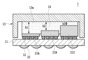
- FIG. 1 is a diagram showing a cross section of a known multi-chip optical module 1.
- the multi-chip optical module 1 includes a substrate 11, IC chips 21A, 21B, and 21C mounted on one surface (mounting surface) of the substrate 11, and a lid component 13 that accommodates the IC chips 21A, 21B, and 21C together with the substrate 11. Contains.
- the IC chips 21A, 21B, and 21C are mounted using bumps 22, and external terminals 12 are formed on the back side of the mounting surface of the substrate 11.
- the plurality of integrated IC chips 21A, 21B, and 21C have different heights.
- Each IC chip 21A, 21B, 21C is connected to the metal lid component 13 with a thermally conductive adhesive. With this configuration, the IC chips 21A, 21B, and 21C are thermally and mechanically connected to the lid component 13.
- the upper surface 13a of the lid component 13 has a constant thickness. Furthermore, the heights of the IC chips 21A, 21B, and 21C are such that the IC chip 21A is the shortest, followed by the IC chip 21B and the IC chip 21C. Therefore, the thickness h1 of the adhesive layer 14 on the IC chip 21A is the thickest, followed by the thickness h2 of the adhesive layer 14 on the IC chip 21B, and the thickness h3 of the adhesive layer 14 on the IC chip 21B. Become thin. It is known that a thermally conductive adhesive has a high thermal resistance, and therefore, if it is thick, it becomes difficult to dissipate heat. In the example shown in FIG. 1, heat is most difficult to dissipate in the adhesive layer 14 on the IC chip 21A, the temperature rises, and the reliability of the multi-chip optical module 1 as a whole is impaired.
- One form of the present invention has been made in view of the above points, and provides a multi-chip module that integrates a plurality of chip components with different heights, which has high heat dissipation, suppresses temperature rise, and improves reliability. Regarding things.
- a multi-chip module is a multi-chip module in which a plurality of chip components mounted on one substrate are packaged, and the multi-chip module accommodates the plurality of chip components together with the substrate.
- a lid component forming a housing space and having a protrusion protruding toward each of the chip components; and a first adhesive layer formed between the protrusion and the chip component; The protrusion length of the protrusion varies depending on the height of the chip component with respect to the substrate.
- FIG. 1 is a diagram showing a cross section of a known multi-chip optical module.
- 1 is a diagram showing a cross section of a multichip optical module according to a first embodiment
- FIG. 7 is a diagram showing a cross section of a multichip optical module according to a second embodiment.
- FIG. 7 is a diagram showing a cross section of a multichip optical module according to a third embodiment.
- FIG. 7 is a diagram showing a cross section of a multichip optical module according to a fourth embodiment.
- FIG. 7 is a diagram showing a cross section of a multichip optical module according to a fifth embodiment.
- FIG. 7 is a diagram showing a cross section of a multichip optical module according to a sixth embodiment.
- FIG. 7 is a diagram showing a cross section of a multichip optical module according to a seventh embodiment.
- the multi-chip module is configured as a multi-chip optical module in which IC chips of optical devices are integrated.
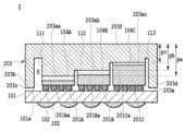
- FIG. 2 is a cross-sectional view for explaining the multi-chip optical module 2 of the first embodiment.
- the multi-chip optical module 2 is configured by packaging a plurality of IC chips 201A, 201B, and 201C, which are chip components mounted on one substrate 101.
- the cross-sectional view shows a cross section of the multi-chip optical module 2 taken in the direction in which the IC chips 201A, 201B, and 201C are arranged.
- the mounting is done by bumps 202.
- the substrate 101 includes external terminals 102 for electrically connecting the IC chips 201A, 201B, and 201C to external equipment.
- the vertical direction is determined so that the mounting surface 101a of the substrate 101 is below the IC chips 201A, 201B, and 201C, that is, the IC chips 201A, 201B, and 201C are mounted on the mounting surface 101a.
- Such an up-down direction is determined regardless of the direction of gravity.
- the IC chips 201A, 201B, and 201C which are optical devices, are constructed by integrating optical elements such as an optical waveguide, an optical modulator, and a semiconductor laser on a single crystal substrate made of silicon or compound semiconductor.
- the multi-chip optical module 2 includes a lid component 203 that forms an accommodation space S that accommodates the IC chips 201A, 201B, and 201C together with the substrate 101.
- the IC chips 201A, 201B, and 201C shown in FIG. 2 have different heights, with the IC chip 201A having the lowest height and the IC chip 201C having the highest height.
- the housing space S only needs to be a space that includes the IC chips 201A, 201B, and 201C, and there is no need to seal the IC chips 201A, 201B, and 201C.
- the lid component 203 has protrusions 111, 112, and 113 that protrude toward each of the IC chips 201A, 201B, and 201C.
- the protrusion lengths of the protrusions 111, 112, and 113 differ depending on the height of the IC chips 201A, 201B, and 201C with respect to the substrate 101.
- the multi-chip optical module 2 includes adhesive layers 104A, 104B, and 104C, which are first adhesive layers formed between the protrusions 111, 112, and 113 and the IC chips 201A, 201B, and 201C. include.
- the lid component 203 includes side walls 203b and 203d around the protrusions 111, 112, and 113.
- the side wall portions 203b and 203d form a series of walls.
- the surface of the side wall portion 203b facing the substrate 101 is referred to as a side wall facing surface 203c, and the surface of the side wall portion 203d facing the substrate 101 is referred to as a side wall facing surface 203e.
- the top surface of the IC chip 201A facing the protrusion 111 is referred to as a chip facing surface 201Aa
- the top surface of the IC chip 201B facing the projection 112 is referred to as a chip facing surface 201Ba
- the top surface of the IC chip 201C facing the projection 113 is referred to as a chip facing surface 201Ca. do.
- the "height" of the IC chips 201A, 201B, and 201C refers to the distance from the mounting surface 101a to the chip facing surfaces 201Aa, 201Ba, and 201Ca of the IC chips 201A, 201B, and 201C, based on the substrate 101 (mounting surface 101a).
- the first embodiment is not limited to such a standard, and the heights of the IC chips 201A, 201B, and 201C may be determined based on one common surface. Note that the height of the IC chip 201A etc. is equal to the thickness of the IC chip 201A etc.
- the protrusion lengths of the protrusions 111, 112, and 113 differ depending on the height of the IC chips 201A, 201B, and 201C with respect to the substrate 101.
- the "protrusion length” is the distance from the common reference position of the protrusions 111, 112, 113 to the protrusion facing surfaces 203aa, 203ab, 203ac of the protrusions 111, 112, 113 facing the IC chips 201A, 201B, 201C. Refers to length.
- the protrusion length is determined based on the upper surface 203f of the lid component 203.
- the first embodiment is not limited to such an example.
- the protrusion length may be determined based on any one of the inner surfaces of the lid component 203, or the protrusion length may be determined based on any surface of the inner surface of the lid component 203, It may be determined based on any one of the surfaces 203aa, 203ab, and 203ac.
- the protrusion length pa of the protrusion 111 on the IC chip 201A having the lowest height is the longest
- the protrusion length pb of the protrusion 112 on the IC chip 201B having the second highest height is the second longest
- the protrusion length pc of the protrusion portion 113 on the IC chip 201C having the longest protrusion length is the shortest.
- the IC chip 201A is fixed to the lid component 203 by the adhesive layer 104A between the chip facing surface 201Aa and the protruding facing surface 203aa.
- the IC chip 201B is fixed to the lid component 203 by the adhesive layer 104B between the chip facing surface 201Ba and the protruding facing surface 203ab
- the IC chip 201C is fixed to the lid component 203 by the adhesive layer 104B between the chip facing surface 201Ca and the protruding facing surface 203ac. It is fixed to the lid component 203 by.
- the thickness of the adhesive layers 104A, 104B, and 104C is made sufficiently thin regardless of the height of the IC chips 201A, 201B, and 201C, and the temperature of the IC chip is suppressed by suppressing heat accumulation in the adhesive layer. Prevent rise. Furthermore, it is possible to prevent malfunctions due to temperature rise of the IC chip, thereby contributing to improving the reliability of the IC chip.
- the first embodiment uses a lid component 203 that is at least partially made of a metal material.
- lid parts include those made of Kovar material, which is an alloy containing iron, nickel, and cobalt, plated with nickel, and those made of a gold-tin alloy.
- Such a lid component 203 has high heat conductivity and heat dissipation, and can further enhance the effect of suppressing the temperature rise of the IC chip.
- FIG. 3 is a cross-sectional view for explaining the multi-chip optical module 3 of the second embodiment.
- the multi-chip optical module 3 is a multi-optical module in which a plurality of IC chips 201A, 201B, and 201C mounted on one substrate 101 are packaged.
- the multi-chip optical module 3 includes a substrate 101 and a lid component 303.
- the substrate 101 and the lid component 303 are overlapped to form a housing space S for the IC chips 201A, 201B, and 201C.
- the lid component 303 includes protrusions 121, 122, and 123 that protrude toward the IC chips 201A, 201B, and 201C, respectively.
- the protruding opposing surface 303aa of the protruding portion 121 faces the IC chip 201A
- the protruding opposing surface 303ab of the protruding portion 122 faces the IC chip 201B
- the protruding opposing surface 303ac of the protruding portion 123 faces the IC chip 201C.
- a series of side walls 303b and 303d are provided around the IC chips 201A, 201B and 201C.
- a side wall facing surface 303c of the side wall portion 303b and a side wall facing surface 303e of the side wall portion 303d face the substrate 101.
- the protrusion 121 is disposed on the IC chip 201A
- the protrusion 122 is disposed on the IC chip 201B
- the protrusion 123 is disposed on the IC chip 201C.
- the lengths of the protrusions 122 and 123 correspond to the heights of the IC chips 201B and 201C, similarly to the first embodiment. That is, the length of the protrusion 122 on the relatively low IC chip 201B is relatively long, and the length of the protrusion 123 on the relatively high IC chip 201C is relatively short. ing.
- the protrusions 121 and 122 have the same protrusion length and are integral.
- the integrated protrusions 121 and 122 are arranged so that, for example, a virtual plane passing between the IC chips 201A and 201B and orthogonal to the substrate 101 intersects with the lid component 303. Differentiate using the surface as the boundary.
- the height of the IC chip 201A is lower than that of the IC chip 201B, and the distance between the chip opposing surface 201Aa and the protruding opposing surface 303aa is wider than the distance between the chip opposing surface 201Ba and the protruding opposing surface 303ab.
- the adhesive layers 104Aa and 104Ab between the IC chip 201A and the protrusion 121 include a spacer 301.
- the total thickness of the adhesive layers 104Aa and 104Ab including the spacer 301 and the height (thickness) of the IC chip 201 is equal to the total thickness of the IC chip 201B and the adhesive layer 104B.
- the spacer 301 may be made of AlN or CuW. Since the spacer 301 has higher processing precision than the lid component 303, the thicknesses of the adhesive layers 104Aa and 104Ab can be adjusted with higher precision to suppress variations. That is, since the lid component 303 is manufactured by cutting the base material, the dimensional tolerance of the step of the protrusion is about 100 ⁇ m. On the other hand, since the spacer 301 is manufactured by cutting and plating a base material, the dimensional tolerance can be suppressed to about 20 ⁇ m. According to the second embodiment, the thicknesses of the adhesive layers 104Aa and 104Ab on the IC chip 201A are adjusted with high precision by making the heights of the protrusions 121 and 122 equal and without providing a step. can be minimized.
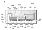
- FIG. 4 is a cross-sectional view for explaining the multi-chip optical module 4 of the third embodiment.
- the multi-chip optical module 4 includes a substrate 101 and a lid component 403.
- the lid component 403 includes protrusions 131, 132, and 133 that protrude toward the IC chips 201A, 201B, and 201C, respectively.
- a protruding opposing surface 403aa of the protruding portion 131 faces the IC chip 201A
- a protruding opposing surface 403ab of the protruding portion 132 faces the IC chip 201B
- a protruding opposing surface 403ac of the protruding portion 133 faces the IC chip 201C.
- a series of side walls 403b and 403d are provided around the IC chips 201A, 201B and 201C.
- a side wall facing surface 403c of the side wall portion 403b and a side wall facing surface 403e of the side wall portion 403d face the substrate 101.
- the protrusions 131 and 132 there is no step between the protrusions 131 and 132, and they are integrated. Further, a spacer 301 is arranged between the IC chip 201A and the protruding opposing surface 403aa, and adhesive layers 104Aa and 104Ac are formed above and below the spacer 301. Further, in the third embodiment, the area of the protruding opposing surface 403aa of the protruding portion 131 is smaller than the area of the chip opposing surface 201Aa, and the area of the protruding opposing surface 403ab of the protruding portion 132 is smaller than the area of the chip opposing surface 201Ba. .
- the adhesive on the chip facing surfaces 201Aa and 201Ba protrudes from the protrusions 131 and 132, respectively, to form adhesive layers 104Ac and 104D having fillets. Therefore, the third embodiment can prevent the adhesive from flowing into the substrate 101 side. Furthermore, the strength of the adhesive between the lid component 403 and the IC chip 201A can be increased.
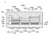
- FIG. 5 is a cross-sectional view for explaining the multi-chip optical module 5 of the fourth embodiment.
- the multi-chip optical module 5 includes a substrate 101 and a lid component 503.
- the lid component 503 includes protrusions 141, 142, and 143 that protrude toward the IC chips 201A, 201B, and 201C, respectively.
- a protruding opposing surface 503aa of the protruding portion 141 faces the IC chip 201A
- a protruding opposing surface 503ab of the protruding portion 142 faces the IC chip 201B
- a protruding opposing surface 503ac of the protruding portion 143 faces the IC chip 201C.
- a series of side walls 503b, 503d are provided around the IC chips 201A, 201B, 201C.
- a side wall facing surface 503c of the side wall portion 503b and a side wall facing surface 503e of the side wall portion 503d face the substrate 101.
- An adhesive layer 104Aa, a spacer 301, and an adhesive layer 104Ad are provided between the protruding opposing surface 503aa and the chip opposing surface 201Aa.
- the fourth embodiment differs from the first embodiment and the like in that the protrusions 141 and 142 each have a stepped portion with a different protrusion length. That is, as shown in FIG. 5, the protruding portion 141 has, in addition to the protruding opposing surface 503aa, a protruding opposing surface 503ad having a shorter protruding length than the protruding opposing surface 503aa.
- the protruding opposing surfaces 503aa and 503ad form a stepped portion 504.
- the protruding portion 142 has a protruding opposing surface 503ae having a shorter protruding length than the protruding opposing surface 503ab.
- the protruding opposing surfaces 503ab and 503ae form a stepped portion 505.
- the area of the protruding opposing surface 503aa is smaller than the area of the chip opposing surface 201Aa, and the area of the protruding opposing surface 503ab is smaller than the area of the chip opposing surface 201Ba. is also smaller.
- the adhesive protrudes from the protrusion 141 and flows into the stepped portion 504, forming the adhesive layer 104Ad having a fillet. Further, the adhesive between the chip facing surface 201Ba and the protruding facing surface 503ab of the IC chip 201B protrudes from the protruding portion 142 and flows into the stepped portion 505, forming an adhesive layer 104E having a fillet. Therefore, the adhesive can be prevented from moving toward the substrate 101, and the strength of the adhesive between the lid component 503 and the IC chip 201A can be increased.
- FIG. 6 is a cross-sectional view for explaining the multi-chip optical module 6 of the fifth embodiment.
- the multi-chip optical module 6 includes a substrate 101 and a lid component 603.
- the lid component 603 includes protrusions 151, 152, and 153 that protrude toward the IC chips 201A, 201B, and 201C, respectively.
- a protruding opposing surface 603aa of the protruding portion 151 faces the IC chip 201A
- a protruding opposing surface 603ab of the protruding portion 152 faces the IC chip 201B
- a protruding opposing surface 603ac of the protruding portion 153 faces the IC chip 201C.
- a series of side walls 603b and 603d are provided around the IC chips 201A, 201B and 201C.
- a side wall facing surface 603c of the side wall portion 603b and a side wall facing surface 603e of the side wall portion 603d face the substrate 101.
- An adhesive layer 104Aa, a spacer 301, and an adhesive layer 104Ab are provided between the protruding opposing surface 603aa and the chip opposing surface 201Aa.
- the fifth embodiment differs from the first embodiment in that an adhesive layer 601 is also formed between the side walls 603b and 603d and the substrate 101, that is, the substrate 101 and the lid component 603 are bonded. .
- the adhesive layer 601 corresponds to the second adhesive layer of the fifth embodiment. According to the fifth embodiment, it is possible to compensate for the decrease in adhesive strength caused by thinning the adhesive layers 104Aa and 104Ab in consideration of the heat dissipation function.
- the side wall opposing surfaces 603c and 603e are closer to the substrate 101 than the protruding opposing surfaces 603aa, 603ab, and 603ac. Therefore, the distance between the lid component 603 and the substrate 101 is relatively narrow, and the thickness of the adhesive layer 601 can be set to a thickness that compensates for the adhesive strength but does not increase the temperature around the IC chip. can.
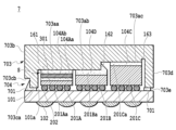
- FIG. 7 is a cross-sectional view for explaining a multi-chip optical module 7 according to the sixth embodiment.
- the multi-chip optical module 7 includes a substrate 101 and a lid component 703.
- the lid component 703 includes protrusions 161, 162, and 163 that protrude toward the IC chips 201A, 201B, and 201C, respectively.
- a protruding opposing surface 703aa of the protruding portion 161 faces the IC chip 201A
- a protruding opposing surface 703ab of the protruding portion 162 faces the IC chip 201B
- a protruding opposing surface 703ac of the protruding portion 163 faces the IC chip 201C.
- a series of side walls 703b and 703d are provided around the IC chips 201A, 201B and 201C.
- Side wall facing surfaces 703ca and 703cb of the side wall portion 703b and side wall facing surface 703e of the side wall portion 703d face the substrate 101.
- the side walls 703b and 703d has a stepped portion 704 having a different distance from the substrate 101, and the stepped portion 704 is closer to the protruding portion 161 etc. than the side closer to the protruding portion 161 etc. It is formed so as to be separated from the substrate 101 on the side far from the substrate 101 . That is, the stepped portion 704 is formed by a side wall opposing surface 703cb that is far from the substrate 101 and a side wall opposing surface 703ca that is closer to the substrate 101 than the side wall opposing surface 703cb.
- the side wall opposing surface 703cb is separated from the substrate 101 on the outside of the lid component 703.
- the adhesive that bonds the substrate 101 and the lid component 703 enters the stepped portion 704 to form a fillet.
- the state of the adhesive layer 701 at the stepped portion 704 can be observed from the outside, thereby facilitating the external appearance inspection.
- FIG. 8 is a cross-sectional view for explaining the multi-chip optical module 8 of the seventh embodiment.
- the multi-chip optical module 8 includes a substrate 101 and a lid component 803.
- the lid component 803 includes protrusions 171, 172, and 173 that protrude toward the IC chips 201A, 201B, and 201C, respectively.
- a protruding opposing surface 803aa of the protruding portion 171 faces the IC chip 201A
- a protruding opposing surface 803ab of the protruding portion 172 faces the IC chip 201B
- a protruding opposing surface 803ac of the protruding portion 173 faces the IC chip 201C.
- a series of side walls 803b and 803d are provided around the IC chips 201A, 201B and 201C.
- Side wall opposing surfaces 803ca and 803b of the side wall portion 803b face the substrate 101.
- the side wall portion 803d has a stepped portion 805 formed by lower surfaces 803ea and 803eb.
- An adhesive is applied between the stepped portion 805 and the substrate 101, and an adhesive layer 801 is further formed between the mounting surface 101a and the lower surface 803eb of the substrate 101, as well as between the side surface 101b of the substrate 101 and the side wall portion 803ea. do.
- Multi-chip optical module 101 Substrate 101a Mounting surface 101b Side surface 102 External terminals 104A, 104B, 104C, 104D, 104Aa, 104Ab, 104Ac, 104Ad, 104Ae, 601, 701 , 801 adhesive layer 111, 112, 113, 121, 122, 123, 131, 132, 133, 141, 142, 143, 151, 152, 153, 161, 162, 163, 171, 172, 173 protrusion 201A, 201B, 201C IC chips 201Aa, 201Ba, 201Ca Chip facing surface 202 Bumps 203, 303, 403, 503, 603, 703, 803 Lid parts 203aa, 203ab, 203ac, 303aa, 303ab, 303ac, 403aa, 403ab, 40 3ac, 503aa, 503ab, 503ac
Landscapes
- Physics & Mathematics (AREA)
- Condensed Matter Physics & Semiconductors (AREA)
- General Physics & Mathematics (AREA)
- Electromagnetism (AREA)
- Optics & Photonics (AREA)
- Semiconductor Lasers (AREA)
Abstract
Description
図2は、第1の実施形態のマルチチップ光モジュール2を説明するための断面図である。マルチチップ光モジュール2は、一つの基板101に実装されたチップ部品である複数のICチップ201A、201B、201Cをパッケージ化して構成されている。断面図は、ICチップ201A、201B、201Cの配置方向にマルチチップ光モジュール2を切断した断面を示している。実装は、バンプ202によって行われる。基板101は、ICチップ201A、201B、201Cを外部機器に電気的に接続するための外部端子102を備えている。以下、本明細書では、基板101の実装面101aがICチップ201A、201B、201Cよりも下、すなわちICチップ201A、201B、201Cは実装面101a上に実装されるように上下方向を決定する。このような上下方向は、重力方向と無関係に決定される。
図3は、第2の実施形態のマルチチップ光モジュール3を説明するための断面図である。マルチチップ光モジュール3は、一つの基板101に実装された複数のICチップ201A、201B、201Cをパッケージ化したマルチ光モジュールである。マルチチップ光モジュール3は、基板101とリッド部品303とを備えている。基板101とリッド部品303は、重ね合わされてICチップ201A、201B、201Cの収容空間Sを形成する。リッド部品303は、ICチップ201A、201B、201Cに向かってそれぞれ突出する突出部121、122、123を備えている。突出部121の突出対向面303aaはICチップ201Aと対向し、突出部122の突出対向面303abはICチップ201Bに向かい、突出部123の突出対向面303acはICチップ201Cに向かう。ICチップ201A、201B、201Cの周囲には一連の側壁部303b、303dが設けられている。側壁部303bの側壁対向面303c、側壁部303dの側壁対向面303eは基板101と対向する。
図4は、第3の実施形態のマルチチップ光モジュール4を説明するための断面図である。マルチチップ光モジュール4は、基板101とリッド部品403とを備えている。リッド部品403は、ICチップ201A、201B、201Cに向かってそれぞれ突出する突出部131、132、133を備えている。突出部131の突出対向面403aaはICチップ201Aと対向し、突出部132の突出対向面403abはICチップ201Bに向かい、突出部133の突出対向面403acはICチップ201Cに向かう。ICチップ201A、201B、201Cの周囲には一連の側壁部403b、403dが設けられている。側壁部403bの側壁対向面403c、側壁部403dの側壁対向面403eは基板101と対向する。
図5は、第4の実施形態のマルチチップ光モジュール5を説明するための断面図である。マルチチップ光モジュール5は、基板101とリッド部品503とを備えている。リッド部品503は、ICチップ201A、201B、201Cに向かってそれぞれ突出する突出部141、142、143を備えている。突出部141の突出対向面503aaはICチップ201Aと対向し、突出部142の突出対向面503abはICチップ201Bに向かい、突出部143の突出対向面503acはICチップ201Cに向かう。ICチップ201A、201B、201Cの周囲には一連の側壁部503b、503dが設けられている。側壁部503bの側壁対向面503c、側壁部503dの側壁対向面503eは基板101と対向する。突出対向面503aaとチップ対向面201Aaとの間には接着剤層104Aa、スペーサ301、接着剤層104Adが設けられている。
図6は、第5の実施形態のマルチチップ光モジュール6を説明するための断面図である。マルチチップ光モジュール6は、基板101とリッド部品603とを備えている。リッド部品603は、ICチップ201A、201B、201Cに向かってそれぞれ突出する突出部151、152、153を備えている。突出部151の突出対向面603aaはICチップ201Aと対向し、突出部152の突出対向面603abはICチップ201Bに向かい、突出部153の突出対向面603acはICチップ201Cに向かう。ICチップ201A、201B、201Cの周囲には一連の側壁部603b、603dが設けられている。側壁部603bの側壁対向面603c、側壁部603dの側壁対向面603eは基板101と対向する。突出対向面603aaとチップ対向面201Aaとの間には接着剤層104Aa、スペーサ301、接着剤層104Abが設けられている。
図7は、第6の実施形態のマルチチップ光モジュール7を説明するための断面図である。マルチチップ光モジュール7は、基板101とリッド部品703とを備えている。リッド部品703は、ICチップ201A、201B、201Cに向かってそれぞれ突出する突出部161、162、163を備えている。突出部161の突出対向面703aaはICチップ201Aと対向し、突出部162の突出対向面703abはICチップ201Bに向かい、突出部163の突出対向面703acはICチップ201Cに向かう。ICチップ201A、201B、201Cの周囲には一連の側壁部703b、703dが設けられている。側壁部703bの側壁対向面703ca、703cb、側壁部703dの側壁対向面703eは基板101と対向する。
図8は、第7の実施形態のマルチチップ光モジュール8を説明するための断面図である。マルチチップ光モジュール8は、基板101とリッド部品803とを備えている。リッド部品803は、ICチップ201A、201B、201Cに向かってそれぞれ突出する突出部171、172、173を備えている。突出部171の突出対向面803aaはICチップ201Aと対向し、突出部172の突出対向面803abはICチップ201Bに向かい、突出部173の突出対向面803acはICチップ201Cに向かう。ICチップ201A、201B、201Cの周囲には一連の側壁部803b、803dが設けられている。側壁部803bの側壁対向面803ca、803bは、基板101と対向する。
101 基板
101a 実装面
101b 側面
102 外部端子
104A,104B,104C,104D,104Aa、104Ab,104Ac,104Ad,104Ae,601,701,801 接着剤層
111,112,113,121,122,123,131,132,133、141,142,143,151,152,153,161,162,163,171,172,173 突出部
201A,201B,201C ICチップ
201Aa,201Ba,201Ca チップ対向面
202 バンプ
203,303,403,503,603,703,803 リッド部品
203aa,203ab,203ac,303aa,303ab,303ac,403aa,403ab,403ac,503aa,503ab,503ac,503ad,503ae,603aa,603ab,603ac,703ab,703ac,803aa,803ab 突出対向面
203b,203d,303b,303d,403b,403d,503b,503d,603b,603d,703b,703d,803b,803d,803ea 側壁部
203c,203e,303c,303e,403c,403e,503c,503e,603c,603e,703c,703e,703ca,703cb,803c 側壁対向面
203f 上面
301 スペーサ
504,505,704,805 段差部
803ea,803eb 下面
S 収容空間
Claims (8)
- 一つの基板に実装された複数のチップ部品をパッケージ化したマルチチップモジュールであって、
前記基板と共に複数の前記チップ部品を収容する収容空間を形成し、前記チップ部品の各々に向かって突出する突出部を有するリッド部品と、
前記突出部と前記チップ部品との間に形成される第1の接着剤層と、を含み、
前記突出部の突出長さが、前記チップ部品の前記基板を基準とした高さに応じて異なっている、マルチチップモジュール。 - 前記チップ部品の少なくとも一つと前記突出部の間の前記第1の接着剤層がスペーサを含み、前記スペーサを含む前記第1の接着剤層と前記チップ部品の厚さの合計は、前記チップ部品の他の一つと、当該他の一つと前記突出部の間の前記第1の接着剤層の厚さの合計と等しい、請求項1に記載のマルチチップモジュール。
- 前記突出部の前記チップ部品に向かう突出対向面の面積は、前記チップ部品の前記突出部に向かうチップ対向面の面積よりも小さい、請求項1または2に記載のマルチチップモジュール。
- 前記突出部の前記チップ部品に向かう突出対向面は、前記突出長さが異なる段差部を有する、請求項1に記載のマルチチップモジュール。
- 前記リッド部品は前記突出部の周囲に配置される側壁部を有し、前記側壁部は前記基板に向かう側壁対向面を有し、前記側壁対向面は、前記突出部の前記基板に向かう突出対向面よりも前記基板に近接し、前記側壁対向面と前記基板の少なくとも一部との間に第2の接着剤層が形成される、請求項1に記載のマルチチップモジュール。
- 前記第2の接着剤層は、前記基板の側面と前記側壁部との間にさらに形成される、請求項5に記載のマルチチップモジュール。
- 前記側壁対向面の少なくとも一部は、前記基板との距離が異なる段差部を有し、前記段差部は、前記側壁対向面のうちの前記突出部に近い側よりも前記突出部から遠い側において前記基板と離れるように形成される、請求項5に記載のマルチチップモジュール。
- 前記リッド部品は、少なくとも一部が金属製である、請求項1に記載のマルチチップモジュール。
Priority Applications (2)
| Application Number | Priority Date | Filing Date | Title |
|---|---|---|---|
| PCT/JP2022/019601 WO2023214468A1 (ja) | 2022-05-06 | 2022-05-06 | マルチチップモジュール |
| JP2024519167A JP7783535B2 (ja) | 2022-05-06 | 2022-05-06 | マルチチップモジュール |
Applications Claiming Priority (1)
| Application Number | Priority Date | Filing Date | Title |
|---|---|---|---|
| PCT/JP2022/019601 WO2023214468A1 (ja) | 2022-05-06 | 2022-05-06 | マルチチップモジュール |
Publications (1)
| Publication Number | Publication Date |
|---|---|
| WO2023214468A1 true WO2023214468A1 (ja) | 2023-11-09 |
Family
ID=88646408
Family Applications (1)
| Application Number | Title | Priority Date | Filing Date |
|---|---|---|---|
| PCT/JP2022/019601 Ceased WO2023214468A1 (ja) | 2022-05-06 | 2022-05-06 | マルチチップモジュール |
Country Status (2)
| Country | Link |
|---|---|
| JP (1) | JP7783535B2 (ja) |
| WO (1) | WO2023214468A1 (ja) |
Citations (4)
| Publication number | Priority date | Publication date | Assignee | Title |
|---|---|---|---|---|
| WO2018079362A1 (ja) * | 2016-10-31 | 2018-05-03 | 信越化学工業株式会社 | 熱伝導性シリコーン組成物、半導体装置及び半導体装置の製造方法 |
| US20180331011A1 (en) * | 2017-05-12 | 2018-11-15 | Globalfoundries Inc. | Flexible heat spreader lid |
| JP2021111718A (ja) * | 2020-01-14 | 2021-08-02 | 株式会社デンソー | 電子機器 |
| WO2021215187A1 (ja) * | 2020-04-23 | 2021-10-28 | 株式会社デンソー | 電子機器 |
-
2022
- 2022-05-06 WO PCT/JP2022/019601 patent/WO2023214468A1/ja not_active Ceased
- 2022-05-06 JP JP2024519167A patent/JP7783535B2/ja active Active
Patent Citations (4)
| Publication number | Priority date | Publication date | Assignee | Title |
|---|---|---|---|---|
| WO2018079362A1 (ja) * | 2016-10-31 | 2018-05-03 | 信越化学工業株式会社 | 熱伝導性シリコーン組成物、半導体装置及び半導体装置の製造方法 |
| US20180331011A1 (en) * | 2017-05-12 | 2018-11-15 | Globalfoundries Inc. | Flexible heat spreader lid |
| JP2021111718A (ja) * | 2020-01-14 | 2021-08-02 | 株式会社デンソー | 電子機器 |
| WO2021215187A1 (ja) * | 2020-04-23 | 2021-10-28 | 株式会社デンソー | 電子機器 |
Also Published As
| Publication number | Publication date |
|---|---|
| JP7783535B2 (ja) | 2025-12-10 |
| JPWO2023214468A1 (ja) | 2023-11-09 |
Similar Documents
| Publication | Publication Date | Title |
|---|---|---|
| US8362607B2 (en) | Integrated circuit package including a thermally and electrically conductive package lid | |
| CN1110094C (zh) | 用于消除电子组件应力的方法和装置 | |
| US7635916B2 (en) | Integrated circuit package with top-side conduction cooling | |
| US20100109152A1 (en) | Electronic device and lid | |
| US20050062166A1 (en) | Single chip and stack-type chip semiconductor package and method of manufacturing the same | |
| CN110301050B (zh) | 热电元件内置封装 | |
| WO2001043167A2 (en) | Low temperature co-fired ceramic-metal packaging technology | |
| JP7703567B2 (ja) | 半導体側面放射レーザー用の密閉表面実装パッケージ、及びその形成方法 | |
| US11923652B2 (en) | Header for semiconductor package, and semiconductor package | |
| JP2008305838A (ja) | 半導体装置及びその実装構造 | |
| US20040036172A1 (en) | Semiconductor device package with integrated heatspreader | |
| US4292647A (en) | Semiconductor package and electronic array having improved heat dissipation | |
| CN112868147B (zh) | 光元件搭载用封装件、电子装置以及电子模块 | |
| US20240274490A1 (en) | Semiconductor module | |
| JP7783535B2 (ja) | マルチチップモジュール | |
| US6747820B2 (en) | Cooling opto-electronic packages | |
| EP4386831B1 (en) | Semiconductor device package and heat dissipating lead frame | |
| CN117855153A (zh) | 半导体器件 | |
| WO2023089059A2 (en) | Laser package and method for manufacturing a laser package | |
| JPH08264688A (ja) | 半導体用セラミックパッケージ | |
| JP2008004688A (ja) | 半導体パッケージ | |
| JP3395126B2 (ja) | Pcカード | |
| WO2021065855A1 (ja) | 光素子搭載用パッケージ、電子装置及び電子モジュール | |
| JP3022738B2 (ja) | マルチチップモジュール | |
| US20230138210A1 (en) | Semiconductor device |
Legal Events
| Date | Code | Title | Description |
|---|---|---|---|
| 121 | Ep: the epo has been informed by wipo that ep was designated in this application |
Ref document number: 22940829 Country of ref document: EP Kind code of ref document: A1 |
|
| WWE | Wipo information: entry into national phase |
Ref document number: 2024519167 Country of ref document: JP |
|
| WWE | Wipo information: entry into national phase |
Ref document number: 18861508 Country of ref document: US |
|
| NENP | Non-entry into the national phase |
Ref country code: DE |
|
| 122 | Ep: pct application non-entry in european phase |
Ref document number: 22940829 Country of ref document: EP Kind code of ref document: A1 |