WO2023210727A1 - 半導体装置 - Google Patents
半導体装置 Download PDFInfo
- Publication number
- WO2023210727A1 WO2023210727A1 PCT/JP2023/016589 JP2023016589W WO2023210727A1 WO 2023210727 A1 WO2023210727 A1 WO 2023210727A1 JP 2023016589 W JP2023016589 W JP 2023016589W WO 2023210727 A1 WO2023210727 A1 WO 2023210727A1
- Authority
- WO
- WIPO (PCT)
- Prior art keywords
- peak
- region
- doping concentration
- recombination center
- semiconductor substrate
- Prior art date
- Legal status (The legal status is an assumption and is not a legal conclusion. Google has not performed a legal analysis and makes no representation as to the accuracy of the status listed.)
- Ceased
Links
Images






Classifications
-
- H—ELECTRICITY
- H10—SEMICONDUCTOR DEVICES; ELECTRIC SOLID-STATE DEVICES NOT OTHERWISE PROVIDED FOR
- H10D—INORGANIC ELECTRIC SEMICONDUCTOR DEVICES
- H10D12/00—Bipolar devices controlled by the field effect, e.g. insulated-gate bipolar transistors [IGBT]
-
- H—ELECTRICITY
- H10—SEMICONDUCTOR DEVICES; ELECTRIC SOLID-STATE DEVICES NOT OTHERWISE PROVIDED FOR
- H10D—INORGANIC ELECTRIC SEMICONDUCTOR DEVICES
- H10D12/00—Bipolar devices controlled by the field effect, e.g. insulated-gate bipolar transistors [IGBT]
- H10D12/411—Insulated-gate bipolar transistors [IGBT]
- H10D12/441—Vertical IGBTs
- H10D12/461—Vertical IGBTs having non-planar surfaces, e.g. having trenches, recesses or pillars in the surfaces of the emitter, base or collector regions
- H10D12/481—Vertical IGBTs having non-planar surfaces, e.g. having trenches, recesses or pillars in the surfaces of the emitter, base or collector regions having gate structures on slanted surfaces, on vertical surfaces, or in grooves, e.g. trench gate IGBTs
-
- H—ELECTRICITY
- H10—SEMICONDUCTOR DEVICES; ELECTRIC SOLID-STATE DEVICES NOT OTHERWISE PROVIDED FOR
- H10D—INORGANIC ELECTRIC SEMICONDUCTOR DEVICES
- H10D30/00—Field-effect transistors [FET]
- H10D30/01—Manufacture or treatment
- H10D30/021—Manufacture or treatment of FETs having insulated gates [IGFET]
-
- H—ELECTRICITY
- H10—SEMICONDUCTOR DEVICES; ELECTRIC SOLID-STATE DEVICES NOT OTHERWISE PROVIDED FOR
- H10D—INORGANIC ELECTRIC SEMICONDUCTOR DEVICES
- H10D30/00—Field-effect transistors [FET]
- H10D30/60—Insulated-gate field-effect transistors [IGFET]
-
- H—ELECTRICITY
- H10—SEMICONDUCTOR DEVICES; ELECTRIC SOLID-STATE DEVICES NOT OTHERWISE PROVIDED FOR
- H10D—INORGANIC ELECTRIC SEMICONDUCTOR DEVICES
- H10D62/00—Semiconductor bodies, or regions thereof, of devices having potential barriers
- H10D62/10—Shapes, relative sizes or dispositions of the regions of the semiconductor bodies; Shapes of the semiconductor bodies
-
- H—ELECTRICITY
- H10—SEMICONDUCTOR DEVICES; ELECTRIC SOLID-STATE DEVICES NOT OTHERWISE PROVIDED FOR
- H10D—INORGANIC ELECTRIC SEMICONDUCTOR DEVICES
- H10D62/00—Semiconductor bodies, or regions thereof, of devices having potential barriers
- H10D62/10—Shapes, relative sizes or dispositions of the regions of the semiconductor bodies; Shapes of the semiconductor bodies
- H10D62/102—Constructional design considerations for preventing surface leakage or controlling electric field concentration
- H10D62/103—Constructional design considerations for preventing surface leakage or controlling electric field concentration for increasing or controlling the breakdown voltage of reverse-biased devices
- H10D62/105—Constructional design considerations for preventing surface leakage or controlling electric field concentration for increasing or controlling the breakdown voltage of reverse-biased devices by having particular doping profiles, shapes or arrangements of PN junctions; by having supplementary regions, e.g. junction termination extension [JTE]
- H10D62/106—Constructional design considerations for preventing surface leakage or controlling electric field concentration for increasing or controlling the breakdown voltage of reverse-biased devices by having particular doping profiles, shapes or arrangements of PN junctions; by having supplementary regions, e.g. junction termination extension [JTE] having supplementary regions doped oppositely to or in rectifying contact with regions of the semiconductor bodies, e.g. guard rings with PN or Schottky junctions
-
- H—ELECTRICITY
- H10—SEMICONDUCTOR DEVICES; ELECTRIC SOLID-STATE DEVICES NOT OTHERWISE PROVIDED FOR
- H10D—INORGANIC ELECTRIC SEMICONDUCTOR DEVICES
- H10D62/00—Semiconductor bodies, or regions thereof, of devices having potential barriers
- H10D62/10—Shapes, relative sizes or dispositions of the regions of the semiconductor bodies; Shapes of the semiconductor bodies
- H10D62/102—Constructional design considerations for preventing surface leakage or controlling electric field concentration
- H10D62/103—Constructional design considerations for preventing surface leakage or controlling electric field concentration for increasing or controlling the breakdown voltage of reverse-biased devices
- H10D62/105—Constructional design considerations for preventing surface leakage or controlling electric field concentration for increasing or controlling the breakdown voltage of reverse-biased devices by having particular doping profiles, shapes or arrangements of PN junctions; by having supplementary regions, e.g. junction termination extension [JTE]
- H10D62/109—Reduced surface field [RESURF] PN junction structures
-
- H—ELECTRICITY
- H10—SEMICONDUCTOR DEVICES; ELECTRIC SOLID-STATE DEVICES NOT OTHERWISE PROVIDED FOR
- H10D—INORGANIC ELECTRIC SEMICONDUCTOR DEVICES
- H10D62/00—Semiconductor bodies, or regions thereof, of devices having potential barriers
- H10D62/10—Shapes, relative sizes or dispositions of the regions of the semiconductor bodies; Shapes of the semiconductor bodies
- H10D62/124—Shapes, relative sizes or dispositions of the regions of semiconductor bodies or of junctions between the regions
- H10D62/126—Top-view geometrical layouts of the regions or the junctions
- H10D62/127—Top-view geometrical layouts of the regions or the junctions of cellular field-effect devices, e.g. multicellular DMOS transistors or IGBTs
-
- H—ELECTRICITY
- H10—SEMICONDUCTOR DEVICES; ELECTRIC SOLID-STATE DEVICES NOT OTHERWISE PROVIDED FOR
- H10D—INORGANIC ELECTRIC SEMICONDUCTOR DEVICES
- H10D62/00—Semiconductor bodies, or regions thereof, of devices having potential barriers
- H10D62/10—Shapes, relative sizes or dispositions of the regions of the semiconductor bodies; Shapes of the semiconductor bodies
- H10D62/13—Semiconductor regions connected to electrodes carrying current to be rectified, amplified or switched, e.g. source or drain regions
- H10D62/141—Anode or cathode regions of thyristors; Collector or emitter regions of gated bipolar-mode devices, e.g. of IGBTs
- H10D62/142—Anode regions of thyristors or collector regions of gated bipolar-mode devices
-
- H—ELECTRICITY
- H10—SEMICONDUCTOR DEVICES; ELECTRIC SOLID-STATE DEVICES NOT OTHERWISE PROVIDED FOR
- H10D—INORGANIC ELECTRIC SEMICONDUCTOR DEVICES
- H10D62/00—Semiconductor bodies, or regions thereof, of devices having potential barriers
- H10D62/10—Shapes, relative sizes or dispositions of the regions of the semiconductor bodies; Shapes of the semiconductor bodies
- H10D62/17—Semiconductor regions connected to electrodes not carrying current to be rectified, amplified or switched, e.g. channel regions
- H10D62/393—Body regions of DMOS transistors or IGBTs
-
- H—ELECTRICITY
- H10—SEMICONDUCTOR DEVICES; ELECTRIC SOLID-STATE DEVICES NOT OTHERWISE PROVIDED FOR
- H10D—INORGANIC ELECTRIC SEMICONDUCTOR DEVICES
- H10D62/00—Semiconductor bodies, or regions thereof, of devices having potential barriers
- H10D62/50—Physical imperfections
- H10D62/53—Physical imperfections the imperfections being within the semiconductor body
-
- H—ELECTRICITY
- H10—SEMICONDUCTOR DEVICES; ELECTRIC SOLID-STATE DEVICES NOT OTHERWISE PROVIDED FOR
- H10D—INORGANIC ELECTRIC SEMICONDUCTOR DEVICES
- H10D62/00—Semiconductor bodies, or regions thereof, of devices having potential barriers
- H10D62/60—Impurity distributions or concentrations
-
- H—ELECTRICITY
- H10—SEMICONDUCTOR DEVICES; ELECTRIC SOLID-STATE DEVICES NOT OTHERWISE PROVIDED FOR
- H10D—INORGANIC ELECTRIC SEMICONDUCTOR DEVICES
- H10D64/00—Electrodes of devices having potential barriers
- H10D64/111—Field plates
- H10D64/117—Recessed field plates, e.g. trench field plates or buried field plates
-
- H—ELECTRICITY
- H10—SEMICONDUCTOR DEVICES; ELECTRIC SOLID-STATE DEVICES NOT OTHERWISE PROVIDED FOR
- H10D—INORGANIC ELECTRIC SEMICONDUCTOR DEVICES
- H10D64/00—Electrodes of devices having potential barriers
- H10D64/20—Electrodes characterised by their shapes, relative sizes or dispositions
- H10D64/27—Electrodes not carrying the current to be rectified, amplified, oscillated or switched, e.g. gates
- H10D64/311—Gate electrodes for field-effect devices
- H10D64/411—Gate electrodes for field-effect devices for FETs
- H10D64/511—Gate electrodes for field-effect devices for FETs for IGFETs
- H10D64/517—Gate electrodes for field-effect devices for FETs for IGFETs characterised by the conducting layers
- H10D64/519—Gate electrodes for field-effect devices for FETs for IGFETs characterised by the conducting layers characterised by their top-view geometrical layouts
-
- H—ELECTRICITY
- H10—SEMICONDUCTOR DEVICES; ELECTRIC SOLID-STATE DEVICES NOT OTHERWISE PROVIDED FOR
- H10D—INORGANIC ELECTRIC SEMICONDUCTOR DEVICES
- H10D8/00—Diodes
-
- H—ELECTRICITY
- H10—SEMICONDUCTOR DEVICES; ELECTRIC SOLID-STATE DEVICES NOT OTHERWISE PROVIDED FOR
- H10D—INORGANIC ELECTRIC SEMICONDUCTOR DEVICES
- H10D8/00—Diodes
- H10D8/50—PIN diodes
-
- H—ELECTRICITY
- H10—SEMICONDUCTOR DEVICES; ELECTRIC SOLID-STATE DEVICES NOT OTHERWISE PROVIDED FOR
- H10D—INORGANIC ELECTRIC SEMICONDUCTOR DEVICES
- H10D84/00—Integrated devices formed in or on semiconductor substrates that comprise only semiconducting layers, e.g. on Si wafers or on GaAs-on-Si wafers
-
- H—ELECTRICITY
- H10—SEMICONDUCTOR DEVICES; ELECTRIC SOLID-STATE DEVICES NOT OTHERWISE PROVIDED FOR
- H10D—INORGANIC ELECTRIC SEMICONDUCTOR DEVICES
- H10D84/00—Integrated devices formed in or on semiconductor substrates that comprise only semiconducting layers, e.g. on Si wafers or on GaAs-on-Si wafers
- H10D84/01—Manufacture or treatment
- H10D84/0123—Integrating together multiple components covered by H10D12/00 or H10D30/00, e.g. integrating multiple IGBTs
- H10D84/0126—Integrating together multiple components covered by H10D12/00 or H10D30/00, e.g. integrating multiple IGBTs the components including insulated gates, e.g. IGFETs
-
- H—ELECTRICITY
- H10—SEMICONDUCTOR DEVICES; ELECTRIC SOLID-STATE DEVICES NOT OTHERWISE PROVIDED FOR
- H10D—INORGANIC ELECTRIC SEMICONDUCTOR DEVICES
- H10D84/00—Integrated devices formed in or on semiconductor substrates that comprise only semiconducting layers, e.g. on Si wafers or on GaAs-on-Si wafers
- H10D84/01—Manufacture or treatment
- H10D84/02—Manufacture or treatment characterised by using material-based technologies
- H10D84/03—Manufacture or treatment characterised by using material-based technologies using Group IV technology, e.g. silicon technology or silicon-carbide [SiC] technology
- H10D84/038—Manufacture or treatment characterised by using material-based technologies using Group IV technology, e.g. silicon technology or silicon-carbide [SiC] technology using silicon technology, e.g. SiGe
-
- H—ELECTRICITY
- H10—SEMICONDUCTOR DEVICES; ELECTRIC SOLID-STATE DEVICES NOT OTHERWISE PROVIDED FOR
- H10D—INORGANIC ELECTRIC SEMICONDUCTOR DEVICES
- H10D84/00—Integrated devices formed in or on semiconductor substrates that comprise only semiconducting layers, e.g. on Si wafers or on GaAs-on-Si wafers
- H10D84/101—Integrated devices comprising main components and built-in components, e.g. IGBT having built-in freewheel diode
- H10D84/141—VDMOS having built-in components
- H10D84/143—VDMOS having built-in components the built-in components being PN junction diodes
- H10D84/144—VDMOS having built-in components the built-in components being PN junction diodes in antiparallel diode configurations
-
- H—ELECTRICITY
- H10—SEMICONDUCTOR DEVICES; ELECTRIC SOLID-STATE DEVICES NOT OTHERWISE PROVIDED FOR
- H10D—INORGANIC ELECTRIC SEMICONDUCTOR DEVICES
- H10D84/00—Integrated devices formed in or on semiconductor substrates that comprise only semiconducting layers, e.g. on Si wafers or on GaAs-on-Si wafers
- H10D84/80—Integrated devices formed in or on semiconductor substrates that comprise only semiconducting layers, e.g. on Si wafers or on GaAs-on-Si wafers characterised by the integration of at least one component covered by groups H10D12/00 or H10D30/00, e.g. integration of IGFETs
- H10D84/82—Integrated devices formed in or on semiconductor substrates that comprise only semiconducting layers, e.g. on Si wafers or on GaAs-on-Si wafers characterised by the integration of at least one component covered by groups H10D12/00 or H10D30/00, e.g. integration of IGFETs of only field-effect components
- H10D84/83—Integrated devices formed in or on semiconductor substrates that comprise only semiconducting layers, e.g. on Si wafers or on GaAs-on-Si wafers characterised by the integration of at least one component covered by groups H10D12/00 or H10D30/00, e.g. integration of IGFETs of only field-effect components of only insulated-gate FETs [IGFET]
-
- H—ELECTRICITY
- H10—SEMICONDUCTOR DEVICES; ELECTRIC SOLID-STATE DEVICES NOT OTHERWISE PROVIDED FOR
- H10P—GENERIC PROCESSES OR APPARATUS FOR THE MANUFACTURE OR TREATMENT OF DEVICES COVERED BY CLASS H10
- H10P36/00—Gettering within semiconductor bodies
Definitions
- the present invention relates to a semiconductor device.
- Patent Documents 1 and 2 Conventionally, a technique is known in which lattice defects are formed by injecting particles such as helium into a semiconductor device (see, for example, Patent Documents 1 and 2).
- Patent Document 1 Patent Document 1
- Patent Document 2 Patent Document 2
- a first aspect of the present invention provides a semiconductor device.
- the semiconductor device may include a semiconductor substrate having an upper surface and a lower surface and having a first conductivity type drift region.
- the semiconductor device may include a buffer region of a first conductivity type that is provided between the drift region and the lower surface of the semiconductor substrate and has a higher doping concentration than the drift region.
- the buffer region may have a first recombination center density peak.
- the buffer region may have a second recombination center density peak located closer to the upper surface of the semiconductor substrate than the first recombination center density peak.
- an integral value of the second recombination center density peak in the depth direction may be larger than an integral value of the first recombination center density peak in the depth direction.
- the buffer region may have a third recombination center density peak located further away from the lower surface of the semiconductor substrate than the second recombination center density peak.
- an integral value of the second recombination center density peak in the depth direction may be larger than an integral value of the third recombination center density peak in the depth direction.
- the peak value of the second recombination center density peak is greater than either the peak value of the first recombination center density peak or the peak value of the third recombination center density peak. It's good that it's big too.
- the buffer region may have one or more doping concentration peaks in the depth direction of the semiconductor substrate.
- the first recombination center density peak may be located between any of the doping concentration peaks and the lower surface of the semiconductor substrate.
- the second recombination center density peak may be located between any of the doping concentration peaks and the upper surface of the semiconductor substrate.
- the one or more doping concentration peaks may include a shallowest doping concentration peak closest to the lower surface of the semiconductor substrate.
- the first recombination center density peak may be located between the shallowest doping concentration peak and the lower surface of the semiconductor substrate.
- the second recombination center density peak may be located between the shallowest doping concentration peak and the upper surface of the semiconductor substrate.
- the buffer region may have three or more of the doping concentration peaks.
- the second recombination center density peak may be located between any two of the doping concentration peaks.
- the third recombination center density peak may be located between any two doping concentration peaks different from the second recombination center density peak.
- the three or more doping concentration peaks may include a first upper surface side doping concentration peak located farthest from the lower surface of the semiconductor substrate. In any of the above semiconductor devices, the three or more doping concentration peaks may include a second upper surface doping concentration peak adjacent to the first upper surface doping concentration peak in the depth direction. In any of the above semiconductor devices, the third recombination center density peak may be located closer to the lower surface of the semiconductor substrate than the second upper surface side doping concentration peak.
- any of the above semiconductor devices there may be no recombination center density peak located between the first upper surface side doping concentration peak and the second upper surface side doping concentration peak.
- the doping concentration peak may be a hydrogen donor concentration peak.
- the doping concentration peak closest to the bottom surface may be a phosphorus concentration peak.
- the doping concentration peak other than the doping concentration peak closest to the lower surface may be a hydrogen donor concentration peak.
- a transistor portion and a diode portion may be arranged in the arrangement direction on the semiconductor substrate.
- the diode section may include the buffer region.
- the transistor section may include the buffer region.
- the integral value of the first recombination center density peak may be the same in the diode section and the transistor section.
- the first recombination center density peak may be a first helium chemical concentration peak.
- the second recombination center density peak may be a second helium chemical concentration peak.
- the third recombination center density peak may be a third helium chemical concentration peak.
- an integral value of the second helium chemical concentration peak in the depth direction may be 1 ⁇ 10 11 (/cm 2 ) or more and 1 ⁇ 10 12 (/cm 2 ) or less.
- an integral value of the first helium chemical concentration peak in the depth direction may be 1 ⁇ 10 11 (/cm 2 ) or more and 1 ⁇ 10 12 (/cm 2 ) or less.
- an integral value of the third helium chemical concentration peak in the depth direction may be 1 ⁇ 10 10 (/cm 2 ) or more and 1 ⁇ 10 11 (/cm 2 ) or less.
- a second aspect of the present invention provides a semiconductor device.
- the semiconductor device may include a semiconductor substrate having an upper surface and a lower surface and having a first conductivity type drift region.
- the semiconductor device may include a buffer region of a first conductivity type that is provided between the drift region and the lower surface of the semiconductor substrate and has a higher doping concentration than the drift region.
- the buffer region has two or more doping concentrations provided at different positions in the depth direction, including the shallowest doping concentration peak located closest to the lower surface of the semiconductor substrate. It may have a peak.
- the buffer region is provided between the lower surface of the semiconductor substrate and the shallowest doping concentration peak and between two doping concentration peaks adjacent in the depth direction.
- the plurality of inter-peak regions may include a first inter-peak region in which one or more first recombination center density peaks are provided. In any of the above semiconductor devices, the plurality of inter-peak regions are arranged farther from the lower surface of the semiconductor substrate than the first inter-peak regions, and one or more second recombination center density peaks are arranged further away from the lower surface of the semiconductor substrate. A second peak-to-peak region may be provided. In any of the above semiconductor devices, the integral value of the recombination center density in the second inter-peak region in the depth direction is greater than the integral value of the recombination center density in the first inter-peak region in the depth direction. It's big and good.
- the integral value of the second helium chemical concentration peak may be greater than or equal to 1 ⁇ 10 11 (/cm 2 ) and less than or equal to 1 ⁇ 10 12 (/cm 2 ).
- the integral value of the first helium chemical concentration peak may be 0.9 ⁇ 10 11 (/cm 2 ) or more and 0.9 ⁇ 10 12 (/cm 2 ) or less.
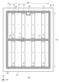
- FIG. 1 is a top view showing an example of a semiconductor device 100.
- FIG. 2 is an enlarged view of region D in FIG. 1.
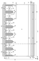
- FIG. 3 is a diagram showing an example of a cross section taken along line ee in FIG. 2.
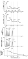
- FIG. 4 is a diagram showing an example of a doping concentration distribution, a hydrogen chemical concentration distribution, and a helium chemical concentration distribution along the line FF in FIG. 3.
- FIG. 3 is a diagram showing the relationship between the ion implantation depth (Rp) and the acceleration energy required for implantation.
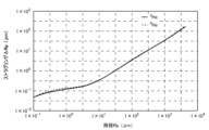
- FIG. 3 is a diagram showing the relationship between the ion implantation depth (Rp) and the straggling ( ⁇ Rp, standard deviation) in the implantation direction.
- FIG. 3 is a diagram showing a first recombination central density peak 220-1 and a second recombination central density peak 220-2.
- 3 is a diagram showing an example of a doping concentration distribution, a hydrogen chemical concentration distribution, a helium chemical concentration distribution, a recombination center density distribution, and an integral concentration distribution of doping concentration in the buffer region 20.
- FIG. 7 is a diagram showing the relationship between the helium dose amount at the first recombination central density peak 220-1 and the second recombination central density peak 220-2 and the reverse recovery loss Err.
- FIG. 7 is a diagram showing the relationship between the helium dose amount and leakage current Ices at a first recombination center density peak 220-1 and a second recombination center density peak 220-2.
- FIG. An example of a carrier concentration distribution and a helium chemical concentration distribution in a buffer region 20 of a comparative example is shown.
- 7 is a diagram showing other examples of doping concentration distribution, hydrogen chemical concentration distribution, helium chemical concentration distribution, recombination center density distribution, and integral concentration distribution of doping concentration in the buffer region 20.
- FIG. FIG. 3 is a diagram illustrating an inter-peak region in a buffer region 20.
- FIG. FIG. 3 is a diagram showing some steps in the method for manufacturing the semiconductor device 100.
- one side in the direction parallel to the depth direction of the semiconductor substrate is referred to as "upper”, and the other side is referred to as “lower”.
- one surface is referred to as the upper surface and the other surface is referred to as the lower surface.
- the “up” and “down” directions are not limited to the gravitational direction or the direction in which the semiconductor device is mounted.
- orthogonal coordinate axes of the X-axis, Y-axis, and Z-axis only specify the relative positions of the components and do not limit specific directions.
- the Z axis does not limit the height direction relative to the ground.
- the +Z-axis direction and the -Z-axis direction are directions opposite to each other.
- the Z-axis direction is described without indicating positive or negative, it means a direction parallel to the +Z-axis and the -Z-axis.
- orthogonal axes parallel to the top and bottom surfaces of the semiconductor substrate are referred to as the X axis and the Y axis. Further, the axis perpendicular to the upper and lower surfaces of the semiconductor substrate is defined as the Z axis.
- the direction of the Z-axis may be referred to as the depth direction.
- a direction parallel to the top and bottom surfaces of the semiconductor substrate, including the X-axis and Y-axis may be referred to as a horizontal direction.
- the region from the center of the semiconductor substrate in the depth direction to the upper surface of the semiconductor substrate may be referred to as the upper surface side.
- the region from the center of the semiconductor substrate in the depth direction to the lower surface of the semiconductor substrate may be referred to as the lower surface side.
- the conductivity type of the doped region doped with impurities is described as P type or N type.
- an impurity may particularly mean either an N-type donor or a P-type acceptor, and may be referred to as a dopant.
- doping means introducing a donor or an acceptor into a semiconductor substrate to make it a semiconductor exhibiting an N-type conductivity type or a semiconductor exhibiting a P-type conductivity type.
- doping concentration refers to the donor concentration or acceptor concentration at thermal equilibrium.
- the net doping concentration means the net concentration obtained by adding together the donor concentration, which is the positive ion concentration, and the acceptor concentration, which is the negative ion concentration, including charge polarity.
- the donor concentration is N D and the acceptor concentration is N A
- the net net doping concentration at any location is N D ⁇ NA .
- the net doping concentration may be simply referred to as doping concentration.
- the donor has the function of supplying electrons to the semiconductor.
- the acceptor has the function of receiving electrons from the semiconductor.
- Donors and acceptors are not limited to impurities themselves.
- a VOH defect in which vacancies (V), oxygen (O), and hydrogen (H) are bonded together in a semiconductor functions as a donor that supplies electrons.
- Sii-H defects caused by interstitial silicon and hydrogen, and CiOi-H defects caused by interstitial carbon, interstitial oxygen, and hydrogen may also function as donors that supply electrons.
- a VOH defect, a Sii-H defect, or a CiOi-H defect may be referred to as a hydrogen donor.
- the semiconductor substrate herein has N-type bulk donors distributed throughout.
- the bulk donor is a donor made from a dopant that is substantially uniformly contained in the ingot during manufacture of the ingot that is the source of the semiconductor substrate.
- the bulk donor in this example is an element other than hydrogen.
- Bulk donor dopants include, but are not limited to, phosphorus, antimony, arsenic, selenium or sulfur.
- the bulk donor in this example is phosphorus.
- Bulk donors are also included in the P-type region.
- the semiconductor substrate may be a wafer cut from a semiconductor ingot, or may be a chip obtained by cutting the wafer into pieces.
- the semiconductor ingot may be manufactured by any one of the Czochralski method (CZ method), the magnetic field Czochralski method (MCZ method), and the float zone method (FZ method).
- the ingot in this example is manufactured by the MCZ method.
- the oxygen concentration contained in the substrate manufactured by the MCZ method is 1 ⁇ 10 17 to 7 ⁇ 10 17 /cm 3 .
- the oxygen concentration contained in the substrate manufactured by the FZ method is 1 ⁇ 10 15 to 5 ⁇ 10 16 /cm 3 .
- Hydrogen donors tend to be generated more easily when the oxygen concentration is high.
- the bulk donor concentration may be a chemical concentration of bulk donors distributed throughout the semiconductor substrate, and may be between 90% and 100% of the chemical concentration.
- the semiconductor substrate may be a non-doped substrate that does not contain a dopant such as phosphorus.
- the bulk donor concentration (D0) of the non-doped substrate is, for example, 1 ⁇ 10 10 /cm 3 or more and 5 ⁇ 10 12 /cm 3 or less.
- the bulk donor concentration (D0) of the non-doped substrate is preferably 1 ⁇ 10 11 /cm 3 or more.
- the bulk donor concentration (D0) of the non-doped substrate is preferably 5 ⁇ 10 12 /cm 3 or less.
- each concentration in the present invention may be a value at room temperature. As an example of the value at room temperature, the value at 300K (Kelvin) (about 26.9°C) may be used.
- the doping concentration when described as P+ type or N+ type, it means that the doping concentration is higher than P type or N type, and when described as P ⁇ type or N ⁇ type, it means that the doping concentration is higher than P type or N type. It means that the concentration is low. Further, in this specification, when it is described as P++ type or N++ type, it means that the doping concentration is higher than that of P+ type or N+ type.
- the unit system in this specification is the SI unit system unless otherwise specified. Although the unit of length is sometimes expressed in cm, various calculations may be performed after converting to meters (m).
- chemical concentration refers to the atomic density of impurities measured regardless of the state of electrical activation.
- the chemical concentration can be measured, for example, by secondary ion mass spectrometry (SIMS).
- the above-mentioned net doping concentration can be measured by voltage-capacitance measurement (CV method).
- the carrier concentration measured by the spreading resistance measurement method (SR method) may be taken as the net doping concentration.
- Carrier means an electron or hole charge carrier.
- the carrier concentration measured by the CV method or the SR method may be a value in a thermal equilibrium state.
- the donor concentration is sufficiently higher than the acceptor concentration, so the carrier concentration in this region may be taken as the donor concentration.
- the carrier concentration in the region may be set as the acceptor concentration.
- the doping concentration of the N-type region may be referred to as a donor concentration
- the doping concentration of the P-type region may be referred to as an acceptor concentration.
- the peak value may be taken as the concentration of donor, acceptor, or net doping in the region.
- the average value of the donor, acceptor, or net doping concentration in the region may be taken as the donor, acceptor, or net doping concentration.
- atoms/cm 3 or /cm 3 is used to express the concentration per unit volume. This unit is used for donor or acceptor concentration or chemical concentration within a semiconductor substrate. The atoms notation may be omitted.
- the carrier concentration measured by the SR method may be lower than the donor or acceptor concentration.
- the carrier mobility of the semiconductor substrate may be lower than the value in the crystalline state.
- the decrease in carrier mobility occurs when carriers are scattered due to disorder of the crystal structure due to lattice defects or the like.
- the reason why the carrier concentration decreases is as follows.
- the SR method the spreading resistance is measured and the carrier concentration is converted from the measured value of the spreading resistance. At this time, the mobility in the crystal state is used as the carrier mobility.
- the carrier concentration is calculated based on the carrier mobility in the crystalline state, although the carrier mobility is reduced. Therefore, the value is lower than the actual carrier concentration, that is, the donor or acceptor concentration.
- the concentration of the donor or acceptor calculated from the carrier concentration measured by the CV method or the SR method may be lower than the chemical concentration of the element representing the donor or acceptor.
- the donor concentration of phosphorus or arsenic as a donor, or the acceptor concentration of boron (boron) as an acceptor is about 99% of these chemical concentrations.
- the donor concentration of hydrogen, which serves as a donor in a silicon semiconductor is about 0.1% to 10% of the chemical concentration of hydrogen.
- FIG. 1 is a top view showing an example of a semiconductor device 100.
- the positions of each member projected onto the upper surface of the semiconductor substrate 10 are shown.
- FIG. 1 only some members of the semiconductor device 100 are shown, and some members are omitted.
- the semiconductor device 100 includes a semiconductor substrate 10.
- the semiconductor substrate 10 is a substrate made of a semiconductor material.
- the semiconductor substrate 10 is a silicon substrate.
- the semiconductor substrate 10 has an edge 162 when viewed from above. In this specification, when simply referred to as a top view, it means viewed from the top surface side of the semiconductor substrate 10.
- the semiconductor substrate 10 of this example has two sets of end sides 162 that face each other when viewed from above. In FIG. 1, the X and Y axes are parallel to either edge 162. Further, the Z axis is perpendicular to the top surface of the semiconductor substrate 10.
- An active part 160 is provided on the semiconductor substrate 10.
- the active portion 160 is a region where a main current flows in the depth direction between the upper surface and the lower surface of the semiconductor substrate 10 when the semiconductor device 100 operates.
- An emitter electrode is provided above the active region 160, but is omitted in FIG.
- the active part 160 is provided with at least one of a transistor part 70 including a transistor element such as an IGBT, and a diode part 80 including a diode element such as a free-wheeling diode (FWD).
- a transistor part 70 including a transistor element such as an IGBT and a diode part 80 including a diode element such as a free-wheeling diode (FWD).
- the transistor sections 70 and the diode sections 80 are alternately arranged along a predetermined arrangement direction (in this example, the X-axis direction) on the upper surface of the semiconductor substrate 10. In other examples, only one of the transistor section 70 and the diode section 80 may be provided in the active section 160.
- the region where the transistor section 70 is arranged is marked with the symbol "I"
- the region where the diode section 80 is arranged is marked with the symbol "F”.
- a direction perpendicular to the arrangement direction in a top view may be referred to as a stretching direction (Y-axis direction in FIG. 1).
- the transistor section 70 and the diode section 80 may each have a length in the extending direction. In other words, the length of the transistor section 70 in the Y-axis direction is greater than the width in the X-axis direction. Similarly, the length of the diode section 80 in the Y-axis direction is greater than the width in the X-axis direction.
- the extending direction of the transistor section 70 and the diode section 80 may be the same as the longitudinal direction of each trench section, which will be described later.
- the diode section 80 has an N+ type cathode region in a region in contact with the lower surface of the semiconductor substrate 10.
- the region provided with the cathode region is referred to as a diode section 80.
- the diode section 80 is a region that overlaps with the cathode region when viewed from above.
- a P+ type collector region may be provided on the lower surface of the semiconductor substrate 10 in a region other than the cathode region.
- the diode section 80 may also include an extension region 81 in which the diode section 80 is extended in the Y-axis direction to a gate wiring to be described later.
- a collector region is provided on the lower surface of the extension region 81.
- the transistor section 70 has a P+ type collector region in a region in contact with the lower surface of the semiconductor substrate 10. Further, in the transistor section 70, a gate structure including an N-type emitter region, a P-type base region, a gate conductive portion, and a gate insulating film is periodically arranged on the upper surface side of the semiconductor substrate 10.
- the semiconductor device 100 may have one or more pads above the semiconductor substrate 10.
- the semiconductor device 100 of this example has a gate pad 164.
- the semiconductor device 100 may have pads such as an anode pad, a cathode pad, and a current detection pad. Each pad is located near the edge 162.
- the vicinity of the edge 162 refers to the area between the edge 162 and the emitter electrode in a top view.
- each pad may be connected to an external circuit via wiring such as a wire.
- a gate potential is applied to the gate pad 164.
- the gate pad 164 is electrically connected to a conductive portion of the gate trench portion of the active portion 160 .
- the semiconductor device 100 includes a gate wiring that connects the gate pad 164 and the gate trench portion. In FIG. 1, the gate wiring is hatched.
- the gate wiring in this example includes an outer gate wiring 130 and an active side gate wiring 131.
- the outer gate wiring 130 is arranged between the active region 160 and the edge 162 of the semiconductor substrate 10 when viewed from above.
- the outer gate wiring 130 of this example surrounds the active region 160 when viewed from above.
- the active portion 160 may be a region surrounded by the outer gate wiring 130 when viewed from above.
- the outer gate wiring 130 is connected to a gate pad 164.
- the outer gate wiring 130 is arranged above the semiconductor substrate 10.
- the outer gate wiring 130 may be a metal wiring containing aluminum or the like.
- the active side gate wiring 131 is provided in the active part 160. By providing the active side gate wiring 131 in the active portion 160, variations in wiring length from the gate pad 164 can be reduced in each region of the semiconductor substrate 10.
- the active side gate wiring 131 is connected to the gate trench part of the active part 160.
- the active side gate wiring 131 is arranged above the semiconductor substrate 10.
- the active side gate wiring 131 may be a wiring formed of a semiconductor such as polysilicon doped with impurities.
- the active side gate wiring 131 may be connected to the outer peripheral gate wiring 130.
- the active side gate wiring 131 in this example extends in the X-axis direction from one outer peripheral gate wiring 130 to the other outer peripheral gate wiring 130 sandwiching the active region 160 so as to cross the active region 160 at approximately the center in the Y-axis direction. It is provided.
- the transistor sections 70 and the diode sections 80 may be arranged alternately in the X-axis direction in each divided region.
- the semiconductor device 100 also includes a temperature sensing section (not shown), which is a PN junction diode made of polysilicon, etc., and a current detection section (not shown), which simulates the operation of a transistor section provided in the active section 160. Good too.
- the semiconductor device 100 of this example includes an edge termination structure portion 90 between the active portion 160 and the end side 162 when viewed from above.
- the edge termination structure section 90 of this example is arranged between the outer peripheral gate wiring 130 and the end side 162.
- the edge termination structure 90 alleviates electric field concentration on the upper surface side of the semiconductor substrate 10.
- the edge termination structure 90 may include at least one of a guard ring, a field plate, and a resurf provided in an annular manner surrounding the active portion 160.
- FIG. 2 is an enlarged view of region D in FIG. 1.
- Region D is a region including the transistor section 70, the diode section 80, and the active side gate wiring 131.
- the semiconductor device 100 of this example includes a gate trench section 40, a dummy trench section 30, a well region 11, an emitter region 12, a base region 14, and a contact region 15 provided inside the upper surface side of a semiconductor substrate 10.
- Each of the gate trench section 40 and the dummy trench section 30 is an example of a trench section.
- the semiconductor device 100 of this example includes an emitter electrode 52 and an active side gate wiring 131 provided above the upper surface of the semiconductor substrate 10. Emitter electrode 52 and active side gate wiring 131 are provided separately from each other.
- An interlayer insulating film is provided between the emitter electrode 52 and the active side gate wiring 131 and the upper surface of the semiconductor substrate 10, but is omitted in FIG. 2.
- a contact hole 54 is provided in the interlayer insulating film of this example, penetrating the interlayer insulating film. In FIG. 2, each contact hole 54 is indicated by diagonal hatching.
- the emitter electrode 52 is provided above the gate trench section 40, dummy trench section 30, well region 11, emitter region 12, base region 14, and contact region 15. Emitter electrode 52 contacts emitter region 12, contact region 15, and base region 14 on the upper surface of semiconductor substrate 10 through contact hole 54. Further, the emitter electrode 52 is connected to a dummy conductive portion within the dummy trench portion 30 through a contact hole provided in the interlayer insulating film. The emitter electrode 52 may be connected to the dummy conductive part of the dummy trench part 30 at the tip of the dummy trench part 30 in the Y-axis direction.
- the active side gate wiring 131 is connected to the gate trench portion 40 through a contact hole provided in the interlayer insulating film.
- the active side gate wiring 131 may be connected to the gate conductive portion of the gate trench portion 40 at the tip portion 41 of the gate trench portion 40 in the Y-axis direction.
- the active side gate wiring 131 is not connected to the dummy conductive part in the dummy trench part 30.
- the emitter electrode 52 is formed of a material containing metal.
- FIG. 2 shows a range where the emitter electrode 52 is provided.
- the emitter electrode 52 is formed of aluminum or an aluminum-silicon alloy, such as a metal alloy such as AlSi or AlSiCu.
- the emitter electrode 52 may include a barrier metal made of titanium, a titanium compound, or the like below a region made of aluminum or the like.
- a plug may be formed by burying tungsten or the like in contact with the barrier metal and aluminum in the contact hole.
- the well region 11 is provided to overlap the active side gate wiring 131.
- the well region 11 is provided extending with a predetermined width even in a range that does not overlap with the active side gate wiring 131.
- the well region 11 in this example is provided away from the end of the contact hole 54 in the Y-axis direction toward the active side gate wiring 131 side.
- the well region 11 is a second conductivity type region having a higher doping concentration than the base region 14 .
- the base region 14 in this example is of P- type, and the well region 11 is of P+ type.
- Each of the transistor section 70 and the diode section 80 has a plurality of trench sections arranged in the arrangement direction.
- the transistor section 70 of this example one or more gate trench sections 40 and one or more dummy trench sections 30 are alternately provided along the arrangement direction.
- the diode section 80 of this example a plurality of dummy trench sections 30 are provided along the arrangement direction.
- the gate trench section 40 is not provided in the diode section 80 of this example.
- the gate trench portion 40 of this example connects two straight portions 39 that extend along the stretching direction perpendicular to the arrangement direction (a portion of the trench that is straight along the stretching direction). It may have a tip 41.
- the stretching direction in FIG. 2 is the Y-axis direction.
- At least a portion of the tip portion 41 be provided in a curved shape when viewed from above.
- the dummy trench section 30 is provided between each straight portion 39 of the gate trench section 40.
- One dummy trench section 30 may be provided between each straight portion 39, or a plurality of dummy trench sections 30 may be provided.
- the dummy trench portion 30 may have a linear shape extending in the extending direction, and may have a linear portion 29 and a tip portion 31 similarly to the gate trench portion 40.
- the semiconductor device 100 shown in FIG. 2 includes both a linear dummy trench section 30 that does not have a tip 31 and a dummy trench section 30 that has a tip 31.
- the diffusion depth of the well region 11 may be deeper than the depths of the gate trench portion 40 and the dummy trench portion 30. Ends of the gate trench section 40 and the dummy trench section 30 in the Y-axis direction are provided in the well region 11 when viewed from above. That is, at the end of each trench portion in the Y-axis direction, the bottom portion of each trench portion in the depth direction is covered with the well region 11 . Thereby, electric field concentration at the bottom of each trench portion can be alleviated.
- a mesa portion is provided between each trench portion in the arrangement direction.
- the mesa portion refers to a region sandwiched between trench portions inside the semiconductor substrate 10.
- the upper end of the mesa portion is the upper surface of the semiconductor substrate 10.
- the depth position of the lower end of the mesa portion is the same as the depth position of the lower end of the trench portion.
- the mesa portion of this example is provided on the upper surface of the semiconductor substrate 10 so as to extend in the extending direction (Y-axis direction) along the trench.
- the transistor section 70 is provided with a mesa section 60
- the diode section 80 is provided with a mesa section 61.
- the mesa portion when the mesa portion is simply referred to, it refers to the mesa portion 60 and the mesa portion 61, respectively.
- a base region 14 is provided in each mesa portion. Among the base regions 14 exposed on the upper surface of the semiconductor substrate 10 in the mesa portion, a region disposed closest to the active side gate wiring 131 is defined as a base region 14-e. In FIG. 2, the base region 14-e is shown arranged at one end of each mesa in the extending direction, but the base region 14-e is also arranged at the other end of each mesa. has been done.
- at least one of the emitter region 12 of the first conductivity type and the contact region 15 of the second conductivity type may be provided in a region sandwiched between the base regions 14-e when viewed from above.
- Emitter region 12 in this example is of N+ type
- contact region 15 is of P+ type.
- Emitter region 12 and contact region 15 may be provided between base region 14 and the upper surface of semiconductor substrate 10 in the depth direction.
- the mesa portion 60 of the transistor portion 70 has an emitter region 12 exposed on the upper surface of the semiconductor substrate 10. Emitter region 12 is provided in contact with gate trench portion 40 . A contact region 15 exposed on the upper surface of the semiconductor substrate 10 may be provided in the mesa portion 60 in contact with the gate trench portion 40 .
- Each of the contact region 15 and emitter region 12 in the mesa portion 60 is provided from one trench portion to the other trench portion in the X-axis direction.
- the contact regions 15 and emitter regions 12 of the mesa section 60 are arranged alternately along the extending direction (Y-axis direction) of the trench section.
- the contact region 15 and emitter region 12 of the mesa portion 60 may be provided in a stripe shape along the extending direction (Y-axis direction) of the trench portion.
- an emitter region 12 is provided in a region in contact with the trench portion, and a contact region 15 is provided in a region sandwiched between the emitter regions 12.
- the mesa portion 61 of the diode portion 80 is not provided with the emitter region 12.
- the base region 14 and the contact region 15 may be provided on the upper surface of the mesa portion 61 .
- a contact region 15 may be provided in a region between the base regions 14-e on the upper surface of the mesa portion 61 in contact with each base region 14-e.
- the base region 14 may be provided in a region sandwiched between the contact regions 15 on the upper surface of the mesa portion 61 .
- the base region 14 may be arranged in the entire region sandwiched between the contact regions 15.
- a contact hole 54 is provided above each mesa portion. Contact hole 54 is arranged in a region sandwiched between base regions 14-e. Contact hole 54 in this example is provided above each of contact region 15, base region 14, and emitter region 12. Contact hole 54 is not provided in a region corresponding to base region 14-e and well region 11.
- the contact hole 54 may be arranged at the center of the mesa portion 60 in the arrangement direction (X-axis direction).
- an N+ type cathode region 82 is provided in a region adjacent to the lower surface of the semiconductor substrate 10.
- a P+ type collector region 22 may be provided in a region where the cathode region 82 is not provided.
- Cathode region 82 and collector region 22 are provided between lower surface 23 of semiconductor substrate 10 and buffer region 20. In FIG. 2, the boundary between the cathode region 82 and the collector region 22 is shown by a dotted line.
- the cathode region 82 is arranged apart from the well region 11 in the Y-axis direction. Thereby, the distance between the P-type region (well region 11), which has a relatively high doping concentration and is formed to a deep position, and the cathode region 82 can be secured, and the breakdown voltage can be improved.
- the end of the cathode region 82 in the Y-axis direction is located farther from the well region 11 than the end of the contact hole 54 in the Y-axis direction.
- the end of the cathode region 82 in the Y-axis direction may be arranged between the well region 11 and the contact hole 54.
- FIG. 3 is a diagram showing an example of the ee cross section in FIG. 2.
- the ee cross section is an XZ plane passing through the emitter region 12 and the cathode region 82.
- the semiconductor device 100 of this example includes a semiconductor substrate 10, an interlayer insulating film 38, an emitter electrode 52, and a collector electrode 24 in the cross section.
- the interlayer insulating film 38 is provided on the upper surface of the semiconductor substrate 10.
- the interlayer insulating film 38 is a film including at least one layer of an insulating film such as silicate glass doped with impurities such as boron or phosphorus, a thermal oxide film, and other insulating films.
- the contact hole 54 described in FIG. 2 is provided in the interlayer insulating film 38.
- the emitter electrode 52 is provided above the interlayer insulating film 38. Emitter electrode 52 is in contact with upper surface 21 of semiconductor substrate 10 through contact hole 54 of interlayer insulating film 38 .
- Collector electrode 24 is provided on lower surface 23 of semiconductor substrate 10 .
- the emitter electrode 52 and the collector electrode 24 are made of a metal material such as aluminum.
- the direction (Z-axis direction) connecting the emitter electrode 52 and the collector electrode 24 is referred to as the depth direction.
- the semiconductor substrate 10 has an N-type or N-type drift region 18. Drift region 18 is provided in each of transistor section 70 and diode section 80.
- an N+ type emitter region 12 and a P ⁇ type base region 14 are provided in order from the upper surface 21 side of the semiconductor substrate 10.
- a drift region 18 is provided below the base region 14 .
- the mesa portion 60 may be provided with an N+ type storage region 16.
- Accumulation region 16 is located between base region 14 and drift region 18 .
- the emitter region 12 is exposed on the upper surface 21 of the semiconductor substrate 10 and is provided in contact with the gate trench portion 40.
- the emitter region 12 may be in contact with the trench portions on both sides of the mesa portion 60.
- Emitter region 12 has a higher doping concentration than drift region 18 .
- the base region 14 is provided below the emitter region 12.
- the base region 14 in this example is provided in contact with the emitter region 12.
- the base region 14 may be in contact with the trench portions on both sides of the mesa portion 60.
- the storage region 16 is provided below the base region 14.
- the accumulation region 16 is an N+ type region having a higher doping concentration than the drift region 18. That is, the accumulation region 16 has a higher donor concentration than the drift region 18.
- the carrier injection promotion effect IE effect
- the storage region 16 may be provided so as to cover the entire lower surface of the base region 14 in each mesa portion 60.
- a P ⁇ type base region 14 is provided in the mesa portion 61 of the diode portion 80 in contact with the upper surface 21 of the semiconductor substrate 10.
- a drift region 18 is provided below the base region 14 .
- the storage region 16 may be provided below the base region 14.
- an N+ type buffer region 20 may be provided under the drift region 18.
- the doping concentration of buffer region 20 is higher than the doping concentration of drift region 18 .
- Buffer region 20 may have a concentration peak with a higher doping concentration than drift region 18 .
- the doping concentration at the concentration peak refers to the doping concentration at the apex of the concentration peak.
- the average value of the doping concentration in a region where the doping concentration distribution is substantially flat may be used as the doping concentration of the drift region 18.
- the buffer region 20 may have two or more concentration peaks in the depth direction (Z-axis direction) of the semiconductor substrate 10.
- the concentration peak of the buffer region 20 may be provided at the same depth position as the chemical concentration peak of hydrogen (protons) or phosphorus, for example.
- Buffer region 20 may function as a field stop layer that prevents a depletion layer spreading from the lower end of base region 14 from reaching P+ type collector region 22 and N+ type cathode region 82.
- the depth position of the upper end of the buffer region 20 is defined as Zf.
- the depth position Zf may be a position where the doping concentration is higher than the doping concentration of the drift region 18.
- a P+ type collector region 22 is provided below the buffer region 20.
- the acceptor concentration in collector region 22 is higher than the acceptor concentration in base region 14 .
- Collector region 22 may contain the same acceptors as base region 14 or may contain different acceptors.
- the acceptor in the collector region 22 is, for example, boron.
- an N+ type cathode region 82 is provided below the buffer region 20.
- the donor concentration in cathode region 82 is higher than the donor concentration in drift region 18 .
- the donor of cathode region 82 is, for example, hydrogen or phosphorus. Note that the elements serving as donors and acceptors in each region are not limited to the above-mentioned examples.
- Collector region 22 and cathode region 82 are exposed on lower surface 23 of semiconductor substrate 10 and connected to collector electrode 24 .
- Collector electrode 24 may be in contact with the entire lower surface 23 of semiconductor substrate 10 .
- the emitter electrode 52 and the collector electrode 24 are formed of a metal material such as aluminum.
- each trench portion extends from the upper surface 21 of the semiconductor substrate 10, penetrates the base region 14, and reaches the drift region 18. In the region where at least one of the emitter region 12, the contact region 15, and the accumulation region 16 is provided, each trench portion also passes through these doped regions and reaches the drift region 18.
- the trench portion penetrating the doping region is not limited to manufacturing in the order in which the doping region is formed and then the trench portion is formed.
- a structure in which a doping region is formed between the trench sections after the trench section is formed is also included in the structure in which the trench section penetrates the doping region.
- the transistor section 70 is provided with the gate trench section 40 and the dummy trench section 30.
- the diode section 80 is provided with the dummy trench section 30 and is not provided with the gate trench section 40.
- the boundary between the diode section 80 and the transistor section 70 in the X-axis direction is the boundary between the cathode region 82 and the collector region 22.
- the gate trench portion 40 includes a gate trench provided on the upper surface 21 of the semiconductor substrate 10, a gate insulating film 42, and a gate conductive portion 44.
- the gate insulating film 42 is provided to cover the inner wall of the gate trench.
- the gate insulating film 42 may be formed by oxidizing or nitriding the semiconductor on the inner wall of the gate trench.
- the gate conductive portion 44 is provided inside the gate trench inside the gate insulating film 42 . That is, the gate insulating film 42 insulates the gate conductive portion 44 and the semiconductor substrate 10.
- Gate conductive portion 44 is formed of a conductive material such as polysilicon.
- the gate conductive portion 44 may be provided longer than the base region 14 in the depth direction.
- the gate trench portion 40 in the cross section is covered with the interlayer insulating film 38 on the upper surface 21 of the semiconductor substrate 10 .
- the gate conductive portion 44 is electrically connected to the gate wiring. When a predetermined gate voltage is applied to the gate conductive portion 44, a channel is formed by an electron inversion layer in the surface layer of the interface of the base region 14 that is in contact with the gate trench portion 40.
- the dummy trench portion 30 may have the same structure as the gate trench portion 40 in the cross section.
- the dummy trench section 30 includes a dummy trench provided on the upper surface 21 of the semiconductor substrate 10, a dummy insulating film 32, and a dummy conductive section 34.
- the dummy conductive portion 34 is electrically connected to the emitter electrode 52.
- the dummy insulating film 32 is provided to cover the inner wall of the dummy trench.
- the dummy conductive portion 34 is provided inside the dummy trench and further inside the dummy insulating film 32 .
- the dummy insulating film 32 insulates the dummy conductive portion 34 and the semiconductor substrate 10.
- the dummy conductive part 34 may be formed of the same material as the gate conductive part 44.
- the dummy conductive portion 34 is formed of a conductive material such as polysilicon.
- the dummy conductive portion 34 may have the same length as the gate conductive portion 44 in the depth direction.
- the gate trench portion 40 and dummy trench portion 30 of this example are covered with an interlayer insulating film 38 on the upper surface 21 of the semiconductor substrate 10.
- the bottoms of the dummy trench section 30 and the gate trench section 40 may have a downwardly convex curved surface (curved in cross section).
- the depth position of the lower end of the gate trench portion 40 is defined as Zt.
- An upper surface side lifetime killer may be provided on the upper surface 21 side of the semiconductor substrate 10.
- the upper surface side lifetime killer is a recombination center of lattice defects etc. formed locally in the depth direction.
- the recombination center density peak 210 in the recombination center density distribution in the depth direction is the upper surface side lifetime killer.
- the peak position of the density distribution of lifetime killers in the depth direction is schematically indicated with a cross. In this specification, the peak position will be described as the position of a lifetime killer.
- the cross marks are arranged discretely in the X-axis direction, the lifetime killers are arranged uniformly in the X-axis direction unless otherwise specified.
- the recombination central density peak 210 can be formed by injecting particles such as helium to a predetermined depth position from the upper surface 21 of the semiconductor substrate 10.
- a concentration peak of particles such as helium may be located at the same depth position as the recombination central density peak 210.
- the central recombination density peak 210 may be located below each trench portion.
- it is preferable that the recombination central density peak 210 is provided at a position that does not overlap with the gate trench portion 40 in a top view. Thereby, the recombination center density peak 210 can be formed by injecting particles such as helium without damaging the gate insulating film 42.
- the recombination center density peak 210 in this example is provided over the entire diode section 80 when viewed from above.
- the central recombination density peak 210 in FIG. 3 is not provided in the transistor section 70, in other examples, the central recombination density peak 210 may be provided in a partial region of the transistor section 70.
- a lower lifetime killer is provided on the lower surface 23 side of the semiconductor substrate 10.
- the lower surface side lifetime killer may be formed by injecting particles such as helium from the lower surface 23 side of the semiconductor substrate 10.
- the recombination center density peak 220 is the bottom side lifetime killer.
- a plurality of recombination central density peaks 220 may be arranged at different positions in the depth direction.
- the first recombination central density peak 220-1 and the second recombination central density peak 220-2 are arranged at different depth positions.
- the recombination central density peaks 220 may be provided at three or more depth positions.
- a helium chemical concentration peak may be provided at the same depth position as each recombination center density peak 220.
- Two or more recombination central density peaks 220 may be provided within the buffer region 20. This makes it easier to control the distribution of lifetime killers within the buffer area 20. Therefore, carrier lifetime can be controlled with high precision.
- the recombination central density peak 220 may be provided throughout the diode section 80 when viewed from above. Further, the recombination central density peak 220 may be provided throughout the transistor section 70 when viewed from above. The recombination center density peak 220 may be provided over the entire active region 160 when viewed from above, or may be provided over the entire semiconductor substrate 10 when viewed from the top. The first recombination central density peak 220-1 and the second recombination central density peak 220-2 may be provided in the same range in a top view.
- FIG. 4A is a diagram showing an example of the doping concentration distribution, hydrogen chemical concentration distribution, helium chemical concentration distribution, and recombination center density distribution on the FF line of FIG. 3.
- the center position of the semiconductor substrate 10 in the depth direction is defined as Zc. That is, the region on the upper surface 21 side of the semiconductor substrate 10 is the region between the upper surface 21 and the center position Zc, and the region on the lower surface 23 side is the region between the lower surface 23 and the center position Zc.
- the emitter region 12 contains an N-type dopant such as phosphorus.
- Base region 14 includes a P-type dopant such as boron.
- Accumulation region 16 includes an N-type dopant, such as phosphorous or hydrogen.
- the doping concentration distribution may have concentration peaks in the emitter region 12, the base region 14, and the accumulation region 16, respectively.
- the drift region 18 is a region where the doping concentration is approximately flat.
- the doping concentration Dd of the drift region 18 may be the same as the bulk donor concentration of the semiconductor substrate 10 or may be higher than the bulk donor concentration.
- the buffer region 20 of this example has a plurality of doping concentration peaks 25-1, 25-2, 25-3, and 25-4 in the doping concentration distribution.
- Each doping concentration peak 25 may be a hydrogen donor peak formed by locally implanting hydrogen ions.
- each doping concentration peak 25 may be formed by implanting an N-type dopant, such as phosphorous.
- the N-type dopant having the doping concentration peak 25-1 closest to the lower surface 23 is phosphorus, and the N-type dopants having the doping concentration peaks 25-1, 25-2, and 25-3 other than the doping concentration peak 25-1 are may be hydrogen.
- the doping concentration peak 25-1 may be a phosphorus concentration peak, and the doping concentration peaks 25 other than the doping concentration peak 25-1 may be hydrogen donor concentration peaks.
- the hydrogen chemical concentration peak 103-1 at the depth position of the doping concentration peak 25-1 may not exist.
- Collector region 22 includes a P-type dopant such as boron.
- Cathode region 82 shown in FIG. 3 also includes an N-type dopant such as phosphorus.
- the hydrogen donor concentration may be determined by subtracting the doping concentration Dd of the drift region 18 from the doping concentration.
- the hydrogen chemical concentration distribution in this example has a plurality of local hydrogen chemical concentration peaks 103 in the buffer region 20.
- a hydrogen donor in which hydrogen, lattice defects, etc. are combined is formed and functions as a donor.
- the hydrogen chemical concentration peak 103 in this example is provided at the same depth position as the doping concentration peak 25. Two peaks being provided at the same depth position means that the apex of one peak is located within the full width at half maximum of one peak. If the concentration of the hydrogen chemical concentration peak 103 is not sufficiently high, a clear doping concentration peak 25 may not be observed at the same depth position as the hydrogen chemical concentration peak 103.
- the hydrogen chemical concentration sharply decreases immediately after entering the drift region 18 from the buffer region 20. Therefore, almost no hydrogen donors are formed in the drift region 18. In other examples, hydrogen may diffuse into the interior of drift region 18 to form hydrogen donors. In this case, the doping concentration of drift region 18 will be higher than the bulk donor concentration.
- the buffer region 20 has two or more helium chemical concentration peaks 221 arranged at different positions in the depth direction of the semiconductor substrate 10.
- a first helium chemical concentration peak 221-1 and a second helium chemical concentration peak 221-2 are provided in the buffer region 20.
- the second helium chemical concentration peak 221-2 is located further away from the lower surface 23 than the first helium chemical concentration peak 221-1.
- a recombination center density peak 220 is formed near each helium chemical concentration peak 221. That is, the first helium chemical concentration peak 221-1 and the second helium chemical concentration peak 221-1 and the second It has a helium chemical concentration peak 221-2.
- Overlapping peaks may mean that the apex of one peak is located within the full width at half maximum of one peak.
- a first recombination central density peak 220-1 and a second recombination central density peak 220-2 are provided in the buffer region 20.
- the second central recombination density peak 220-2 is located further away from the lower surface 23 (that is, closer to the upper surface 21) than the first central recombination density peak 220-1.
- Recombination center density peak 220 may be a recombination center that promotes carrier recombination.
- the recombination center may be a lattice defect.
- the lattice defects may be mainly vacancies such as monoatomic vacancies (V) and multiatomic vacancies (VV), may be dislocations, may be interstitial atoms, may be transition metals, etc. .
- lattice defects may include donors and acceptors, but in this specification, lattice defects mainly composed of vacancies are sometimes referred to as vacancy-type lattice defects, vacancy-type defects, or simply lattice defects. In this specification, lattice defects are sometimes simply referred to as recombination centers or lifetime killers as recombination centers that contribute to carrier recombination.
- the lifetime killer may be formed by implanting helium ions into the semiconductor substrate 10. Since the lifetime killer formed by injecting helium may be terminated by hydrogen existing in the buffer region 20, the depth position of the lifetime killer density peak and the depth of the helium chemical concentration peak 221 It may not match the position.
- Each depth location may be implanted with 3 He or 4 He.
- 3He is a helium isotope containing two protons and one neutron.
- 4He is a helium isotope containing two protons and two neutrons.
- the half-width in the depth direction of the concentration peak of the helium chemical concentration can be reduced. can be made smaller.
- FIG. 4B is a diagram showing the relationship between the ion implantation depth (Rp) and the acceleration energy required for implantation.
- Rp ion implantation depth
- helium ions are directly implanted into the silicon semiconductor substrate 10 without going through a buffer material.
- the horizontal axis in FIG. 4B is the range Rp ( ⁇ m), and the vertical axis is the acceleration energy E (eV) required for implantation.
- E acceleration energy required for implantation.
- FIG. 4B an example of 3 He is shown with a solid line, and an example of 4 He is shown with a dashed line.
- E be the acceleration energy calculated by substituting the actual range Rp' at the time of manufacturing the semiconductor device 100 into equation (1). If the actual acceleration energy E' during manufacturing is within ⁇ 20% of the acceleration energy E calculated from equation (1), it may be considered that 3 He is used.
- the acceleration energy of 4 He is higher than the acceleration energy of 3 He. is also about 10% higher.
- the acceleration energy of 3He is about 10% higher than the acceleration energy of 4He . It is presumed that this is because the balance between electronic stopping power and nuclear stopping power changes depending on the number of neutrons in the isotope.
- the range Rp is 10 ⁇ m or less, 4 He may be used. This makes it possible to implant helium ions with an acceleration energy that is about 10% lower. If the range Rp is greater than 10 ⁇ m, 3 He may be used.
- FIG. 4C is a diagram showing the relationship between the ion implantation depth (Rp) and the straggling in the implantation direction ( ⁇ Rp, standard deviation).
- the injection direction in this example is the depth direction of the semiconductor substrate 10.
- helium ions are directly implanted into the silicon semiconductor substrate 10 without going through a buffer material.
- the horizontal axis in FIG. 4C is the range Rp ( ⁇ m), and the vertical axis is the straggling ⁇ Rp ( ⁇ m).
- the 3 He example is shown as a solid line
- the 4 He example is shown as a dashed line.
- the straggling ⁇ Rp may be calculated assuming that the helium concentration distribution is a Gaussian distribution.
- the straggling ⁇ Rp may be the distance (distribution width) between two points where the density is 0.60653 times the density peak value, or it may be the distance between two points where the density is 0.6 times the density peak value. . If the minimum value or the like between adjacent concentration peaks is larger than 0.6 times the concentration peak value, the distance between the inflection points such as the minimum value of the concentration distribution may be set as the straggling ⁇ Rp.
- ⁇ Rp be the stranding calculated by substituting the actual range Rp' at the time of manufacturing the semiconductor device 100 into equation (3). If the actual straggling ⁇ Rp' during manufacturing is within ⁇ 20% of the straggling ⁇ Rp calculated from equation (3), it may be considered that 3 He is used. It is preferable that the actual straggling ⁇ Rp' does not include helium diffusion due to thermal annealing.
- the actual straggling ⁇ Rp' may be a value measured after helium implantation and before thermal annealing, or may be a value obtained by subtracting the amount of helium diffusion from the value measured after thermal annealing. .
- the range Rp is the boundary value in the range of 10 to 20 ⁇ m, and the range Rp is less than the boundary value, the 3 He straggling ⁇ Rp is better than the 4 He straggling ⁇ Rp. It is about 10% smaller than that.
- the straggling ⁇ Rp is approximately equal between 3 He and 4 He. It is presumed that this is because the balance between electronic stopping power and nuclear stopping power changes depending on the number of neutrons in the isotope.
- the range Rp when the range Rp is 20 ⁇ m or less, 3 He may be used. This makes it possible to reduce the straggling ⁇ Rp by about 10%.
- a difference of about 10% in the straggling ⁇ Rp has a sufficiently small difference in helium chemical concentration distribution or electrical properties, even if the range Rp is 20 ⁇ m or less, the straggling between 3 He and 4 He
- the rings ⁇ Rp may be considered to be approximately equal.
- the helium atoms implanted into the semiconductor substrate 10 may be 3 He or 4 He.
- the full width at half maximum of the helium chemical concentration peak 221 when 4 He is implanted is 1 ⁇ m or less.
- the full width at half maximum of the helium chemical concentration peak 221 may be 0.5 ⁇ m or less.
- the total concentration of recombination center density peaks 220 can be maintained high. Therefore, the lifetime of carriers can be shortened and tail current can be suppressed when the semiconductor device 100 is turned off or the like.
- the straggling ⁇ Rp becomes 10 ⁇ m or more.
- the acceleration energy E of 4 He is approximately 21 MeV or more (range Rp is 250 ⁇ m or more)
- the straggling ⁇ Rp is 10 ⁇ m or more.
- the full width at half maximum of the helium chemical concentration peak 221 cannot be made sufficiently smaller than the width of the buffer region 20 in the depth direction. For this reason, hydrogen donors are formed in a wide range of the buffer region 20, and the doping concentration distribution fluctuates. For this reason, an electric field may be locally concentrated in the buffer region 20 during a short circuit, and the short circuit current withstand capacity may be reduced.
- the acceleration energy E when implanting either 3 He or 4 He, the acceleration energy E may be 20 MeV or less, or 10 MeV or less.
- the acceleration energy E of at least one or more or more helium chemical concentration peaks 221 among the plurality of helium chemical concentration peaks 221 may be 10 MeV or less, and may be 5 MeV or less.
- FIG. 5 is a diagram showing the first recombination center density peak 220-1 and the second recombination center density peak 220-2.
- the peak value of the first recombination center density peak 220-1 is assumed to be Pk1
- the peak value of the second recombination center density peak 220-2 is assumed to be Pk2.
- the integral value of the first central recombination density peak 220-1 in the depth direction is S1
- the integral value of the second central recombination density peak 220-2 in the depth direction is S2.
- the integral value S1 may be a value obtained by integrating the range where the recombination center density is equal to or greater than ⁇ Pk1 (the hatched range in FIG.
- the coefficient ⁇ is a real number greater than 0 and less than 1.
- the integral value S1 is a value obtained by integrating the first recombination center density peak 220-1 over the full width at half maximum.
- the integral value S2 may be a value obtained by integrating the range in which the recombination center density is equal to or greater than ⁇ Pk2 at the second recombination center density peak 220-2.
- the coefficient ⁇ may be the same for each recombination center density peak 220.
- the coefficient ⁇ may be 0.5, 0.1, 0.01, or some other numerical value.
- the distribution of recombination center density may be calculated from the distribution of carrier lifetimes, or may be measured using other methods.
- the distribution of the recombination center density for example, the vacancy concentration measured by the positron annihilation method may be used as the recombination center density.
- the atomic density of helium atoms measured by the SIMS method may be used as the recombination center density.
- the integral value S2 of the second central recombination density peak 220-2 in this example is larger than the integral value S1 of the first central recombination density peak 220-1.
- Each integral value can be adjusted by adjusting the dose of the charged particle beam, such as helium, injected into each depth position. By increasing the integral value S2, the reverse recovery loss Err can be greatly reduced.
- the integral value S2 may be twice or more, five times or more, or ten times or more as the integral value S1.
- the peak value Pk2 of the second recombination center density peak 220-2 in this example may be larger than the peak value Pk1 of the first recombination center density peak 220-1. At least one of the conditions of integral value S2>integral value S1 and the condition of peak value Pk2>peak value Pk1 may be satisfied, or both may be satisfied.
- the peak value Pk2 may be twice or more, five times or more, or ten times or more as the peak value Pk1.
- the peak value of the first helium chemical concentration peak 221-1 may be smaller than the peak value of the second helium chemical concentration peak 221-2, and may be the same as the peak value of the second helium chemical concentration peak 221-2. It may be greater than the peak value of the second helium chemical concentration peak 221-2. Recombination centers formed by helium irradiation may be terminated with hydrogen and become hydrogen donors. Therefore, even if the peak value of the first helium chemical concentration peak 221-1 is the same as or larger than the peak value of the second helium chemical concentration peak 221-2, the difference in hydrogen concentration at each position will cause the integration It is possible that value S2>integral value S1, or peak value Pk2>peak value Pk1.
- FIG. 6 is a diagram showing an example of the doping concentration distribution, hydrogen chemical concentration distribution, helium chemical concentration distribution, recombination center density distribution, and integral concentration distribution of doping concentration in the buffer region 20.
- the integrated concentration distribution in this example is a distribution of integral values (/cm 2 ) obtained by integrating the doping concentration from the lower end position Zt of the trench portion toward the lower surface 23.
- the lower end position Zt is set at the PN junction between the P-type layer and the drift region 18 located on the lower surface 23 side of the semiconductor substrate 10. Good location.
- the integrated concentration distribution of this example is defined as the integral value (/ cm 2 ) distribution.
- the doping concentration distribution in this example has one or more doping concentration peaks 25-1, 25-2, 25-3, and 25-4 in order from the lower surface 23 side of the semiconductor substrate 10.
- the doping concentration peak 25-1 is an example of the shallowest doping concentration peak closest to the lower surface 23 among the doping concentration peaks 25 of the buffer region 20.
- the doping concentration peak 25-4 is an example of the deepest doping concentration peak located farthest from the lower surface 23.
- the depth positions of the respective doping concentration peaks 25 are designated as Zd1, Zd2, Zd3, and Zd4 in order from the lower surface 23 side. Each depth position Zd indicates a distance from the lower surface 23. Note that any one of the doping concentration peaks 25 does not have to be a clear peak.
- the doping concentration peak 25 may be an inflection point (kink) of the slope of the doping concentration distribution.
- the doping concentration peak 25-1 may be the doping concentration peak 25 having the maximum concentration value.
- the doping concentration peak 25-2 may be the doping concentration peak 25 having the second largest concentration value.
- the doping concentration peak 25-3 may be the doping concentration peak 25 with the minimum concentration value.
- the doping concentration peak 25-4 may be a higher doping concentration peak 25 than the doping concentration peak 25-3.
- the hydrogen chemical concentration distribution in this example has hydrogen chemical concentration peaks 103-1, 103-2, 103-3, and 103-4 in order from the lower surface 23 side of the semiconductor substrate 10.
- the depth positions of the respective hydrogen chemical concentration peaks 103 are designated as Zh1, Zh2, Zh3, and Zh4 in order from the lower surface 23 side.
- Each depth position Zh indicates a distance from the lower surface 23.
- Depth position Zdk may be the same as depth position Zhk. However, k is an integer from 1 to 4.
- the hydrogen chemical concentration peak 103-1 may be the hydrogen chemical concentration peak 103 with the maximum concentration value.
- the hydrogen chemical concentration peak 103-2 may be the hydrogen chemical concentration peak 103 having the second largest concentration value.
- the hydrogen chemical concentration peak 103-3 may be the hydrogen chemical concentration peak 103 with the minimum concentration value.
- the hydrogen chemical concentration peak 103-4 may be a hydrogen chemical concentration peak 103 with a higher concentration than the hydrogen chemical concentration peak 103-3.
- the helium chemical concentration distribution in this example has a first helium chemical concentration peak 221-1 and a second helium chemical concentration peak 221-2 in order from the lower surface 23 side of the semiconductor substrate 10.
- the recombination center density distribution of this example has a first recombination center density peak 220-1 and a second recombination center density peak 220-2 in order from the lower surface 23 side of the semiconductor substrate 10.
- the depth positions of the respective helium chemical concentration peaks 221 are defined as Zk1 and Zk2 in order from the lower surface 23 side.
- the depth positions of the respective recombination central density peaks 220 may be set to Zk1 and Zk2 in order from the lower surface 23 side. Each depth position Zk indicates a distance from the lower surface 23.
- the first recombination central density peak 220-1 is located between any doping concentration peak 25 and the lower surface 23 of the semiconductor substrate 10, and the second recombination central density peak 220-2 is located between the doping concentration peak 25 and the lower surface 23 of the semiconductor substrate 10. It is arranged between the peak 25 and the upper surface 21.
- the first recombination central density peak 220-1 is located closer to the lower surface 23 than the doping concentration peak 25-1
- the second recombination central density peak 220-2 is located closer to the doping concentration peak 25-1. 1 is disposed closer to the upper surface 21.
- the second recombination center density peak 220-2 is located between the doping concentration peak 25-1 and the doping concentration peak 25-2.
- the second recombination center density peak 220-2 may be located between the doping concentration peak 25-2 and the doping concentration peak 25-3; 25-4. That is, only one doping concentration peak 25 may be arranged between the first recombination central density peak 220-1 and the second recombination central density peak 220-2, and a plurality of doping concentration peaks 25 may be arranged. may be done. As will be described later, by arranging the first recombination center density peak 220-1 closer to the lower surface 23 than the doping concentration peak 25-1, reverse recovery loss can be suppressed while suppressing leakage current. Further, by arranging the second recombination center density peak 220-2 closer to the upper surface 21 than the doping concentration peak 25-1, reverse recovery loss can be significantly reduced.
- the doping concentration distribution may have a valley portion 35 at the same depth position as any of the helium chemical concentration peaks 221.
- the valley portion 35 is a region where the doping concentration exhibits a minimum value.
- the valley portion 35 is omitted at the same depth position as the helium chemical concentration peak 221, but the valley portion 35 may be provided.
- the depletion layer edge position Ze is a depth position at which the integrated concentration obtained by integrating the net doping concentrations of the drift region 18 and the buffer region 20 from the upper end of the drift region 18 toward the lower surface 23 of the semiconductor substrate 10 reaches the critical integrated concentration n c It is.
- the depletion layer edge position Ze may be referred to as the critical concentration depth position Ze.
- the critical integrated concentration when a forward bias is applied between the collector electrode 24 and the emitter electrode 52 and avalanche breakdown occurs, and when the area from the upper end of the drift region 18 to a specific position of the buffer region 20 is depleted, the drift The value obtained by integrating the net doping concentration from the upper end of the region 18 to the specific position is referred to as the critical integrated concentration.
- the depletion layer edge position Ze is the position closest to the lower surface 23 that the depletion layer that spreads from the lower end of the base region 14 toward the lower surface 23 of the semiconductor substrate 10 reaches when avalanche breakdown occurs.
- the critical integrated concentration n c depends on the constituent atoms of the semiconductor substrate 10 .
- the critical integrated concentration n c is approximately 1.2 ⁇ 10 12 /cm 2 .
- the position closest to the lower surface 23 that the depletion layer reaches may be defined as the depletion layer edge position Ze.
- the upper end of the drift region 18 is the boundary position between the drift region 18 and the accumulation region 16 in the example shown in FIG. If it is difficult to determine the boundary position between the drift region 18 and the accumulation region 16, the lower end position Zt of the trench portion may be set as the lower end of the drift region 18. Further, when the drift region 18 and the base region 14 are in contact with each other, the position of the PN junction at the boundary between the drift region 18 and the base region 14 is the upper end of the drift region 18 .
- the depletion layer edge position Ze may be located between the first recombination center density peak 220-1 and the second recombination center density peak 220-2.
- the depletion layer edge position Ze may be located between the doping concentration peak 25-1 and the doping concentration peak 25-2.
- the integral value of the recombination center density closer to the upper surface 21 than the critical concentration depth position Ze may be greater than or equal to the integral value of the recombination center density closer to the lower surface 23 than the critical concentration depth position Ze, It can be small.
- the integral value of the recombination center density closer to the upper surface 21 than the critical concentration depth position Ze is larger than the integral value of the recombination center density closer to the lower surface 23 than the critical concentration depth position Ze.
- the integral value of the helium chemical concentration on the upper surface 21 side from the critical concentration depth position Ze may be greater than, equal to, or smaller than the integral value of the helium chemical concentration on the lower surface 23 side than the critical concentration depth position Ze. Good too.
- the integral value of the helium chemical concentration closer to the upper surface 21 than the critical concentration depth position Ze is larger than the integral value of the helium chemical concentration closer to the lower surface 23 than the critical concentration depth position Ze.
- FIG. 7 is a diagram showing the relationship between the helium dose and the reverse recovery loss Err at the first recombination central density peak 220-1 and the second recombination central density peak 220-2.
- the arrangement of the first recombination central density peak 220-1 and the second recombination central density peak 220-2 is similar to the example shown in FIG. 4A.
- each recombination center density peak 220 When the helium dose is increased, the integral value S and peak value Pk of each recombination center density peak 220 increase.
- the reverse recovery loss Err refers to the loss during reverse recovery of the diode section 80.
- circles indicate the results of changing the helium dose for the first recombination center density peak 220-1 while maintaining the helium dose for the second recombination center density peak 220-2.
- the result of changing the helium dose amount for the second recombination center density peak 220-2 while maintaining the helium dose amount for the first recombination center density peak 220-1 is indicated by a cross mark.
- reverse recovery loss can be reduced. As shown in FIG. 7, reverse recovery loss can be significantly reduced by increasing the helium dose for the second recombination center density peak 220-2 than for the first recombination center density peak 220-1. .
- FIG. 8 is a diagram showing the relationship between the helium dose and leakage current Ices at the first recombination center density peak 220-1 and the second recombination center density peak 220-2.
- the arrangement of the first recombination central density peak 220-1 and the second recombination central density peak 220-2 is similar to the example shown in FIG. 4A.
- the measurement conditions in the plots of circles and crosses in FIG. 8 are the same as in the example of FIG. 7.
- the leakage current Ices is also referred to as the collector-emitter cutoff current.
- the leakage current Ices is a leakage current between the collector and the emitter when a predetermined voltage is applied between the collector and the emitter in a state where the gate and the emitter are short-circuited (that is, the transistor section 70 is in an off state).
- leakage current may increase through the recombination center.
- the buffer region 20 may be provided in both the diode section 80 and the transistor section 70.
- the integral value S1 of the first recombination center density peak 220-1 may be the same.
- the structure of the buffer region 20 may be the same in the diode section 80 and the transistor section 70. In this case, if the integral value S1 or the peak value Pk1 of the first recombination center density peak 220-1 is made too large, carrier injection from the collector region 22 of the transistor section 70 is inhibited, resulting in a carrier injection promoting effect (IE effect). ) becomes low, and the on-voltage of the transistor section 70 increases.
- IE effect carrier injection promoting effect
- FIG. 9 shows an example of the carrier concentration distribution and helium chemical concentration distribution in the buffer region 20 of the comparative example.
- the buffer region 20 of this example has only one helium chemical concentration peak formed by implanting 3 He.
- the carrier concentration distribution when helium is not implanted is shown by a solid line, and the carrier concentration distribution when helium is implanted is shown by a broken line.
- the carrier concentration distribution when helium is not implanted is similar to the doping concentration distribution in FIG. 6 and the like.
- the buffer region 20 is provided with a single helium chemical concentration peak. This makes it difficult to control the distribution of lifetime killers.
- hydrogen donors which are bonds between recombination centers and hydrogen
- the carrier concentration distribution fluctuates over a wide range compared to when no helium is injected. Put it away.
- the helium distribution spreads to the vicinity of the upper end of the buffer region 20 a convex portion appears in the carrier concentration distribution, and the characteristics of the semiconductor device 100, such as a decrease in avalanche resistance, may deviate from the designed values.
- a plurality of helium chemical concentration peaks are arranged in the buffer region 20, so that the distribution of lifetime killer can be adjusted with high accuracy. Further, by reducing the half width of the helium chemical concentration peak, it is possible to suppress fluctuations in the carrier concentration distribution over a wide range.
- FIG. 10 is a diagram showing other examples of the doping concentration distribution, hydrogen chemical concentration distribution, helium chemical concentration distribution, recombination center density distribution, and integral concentration distribution of doping concentration in the buffer region 20.
- the buffer region 20 of this example differs from the buffer region 20 described in FIGS. 1 to 9 in that it further includes a third helium chemical concentration peak 221-3 and a third recombination density peak 220-3.
- Other structures are similar to the buffer area 20 of any of the embodiments described in FIGS. 1 to 9.
- the third helium chemical concentration peak 221-3 and the third recombination density peak 220-3 are located at depth position Zk3.
- the peak value of the third recombination density peak 220-3 is assumed to be Pk3.
- the third recombination central density peak 220-3 is located further away from the lower surface 23 of the semiconductor substrate 10 than the second recombination central density peak 220-2.
- the integral value S2 of the second central recombination density peak 220-2 in the depth direction is larger than the integral value S3 of the third central recombination density peak 220-3 in the depth direction.
- the integral value S3 is a value obtained by integrating the range in which the recombination center density is equal to or greater than ⁇ Pk3 in the third recombination center density peak 220-3, as in the example explained in FIG.
- the coefficient ⁇ may be the same as other recombination center density peaks 220.
- the reverse recovery loss Err can be further reduced.
- the integral value S of the recombination center density peak 220 at a position far from the lower surface 23 is increased too much, as explained in FIG. Convex portions may occur in the carrier density distribution.
- the integral value S3 of the third recombination central density peak 220-3 smaller than the integral value S2 of the second recombination central density peak 220-2, the reverse recovery loss Err can be efficiently reduced.
- the integral value S2 may be twice or more, five times or more, or ten times or more as the integral value S3.
- the peak value Pk2 of the second recombination center density peak 220-2 may be larger than the peak value Pk3 of the third recombination center density peak 220-3. At least one of the conditions of integral value S2>integral value S3 and the condition of peak value Pk2>peak value Pk3 may be satisfied, or both may be satisfied.
- the peak value Pk2 may be twice or more, five times or more, or ten times or more as the peak value Pk3.
- the peak value Pk1 of the second recombination center density peak 220-2 is either the peak value Pk1 of the first recombination center density peak 220-1 or the peak value Pk3 of the third recombination center density peak 220-3. It's better to be bigger than that.
- the integral value S2 of the second recombination central density peak 220-2 is either the integral value S1 of the first recombination central density peak 220-1 or the integral value S3 of the third recombination central density peak 220-3. It's better to be bigger than that.
- the integral value S1 of the first recombination central density peak 220-1 and the integral value S3 of the third recombination central density peak 220-3 may be larger or may be the same.
- the peak value Pk1 of the first recombination center density peak 220-1 and the peak value Pk3 of the third recombination center density peak 220-3 may be larger or may be the same.
- the buffer region 20 of this example has three or more doping concentration peaks 25.
- the second recombination central density peak 220-2 may be located between any two doping concentration peaks.
- the second recombination central density peak 220-2 is located between the doping concentration peak 25-1 and the doping concentration peak 25-2.
- the third recombination central density peak 220-3 may be located between any two doping concentration peaks 25 different from the second recombination central density peak 220-2.
- the third recombination center density peak 220-3 is located between the doping concentration peak 25-2 and the doping concentration peak 25-3.
- doping concentration peak 25 may be placed between the second recombination center density peak 220-2 and the third recombination center density peak 220-3.
- a plurality of doping concentration peaks 25 may be arranged between the second recombination central density peak 220-2 and the third recombination central density peak 220-3.
- the doping concentration peak 25-4 located farthest from the lower surface 23 of the semiconductor substrate 10 is set as the first upper surface side doping concentration peak
- the doping concentration peak 25-4 adjacent to the doping concentration peak 25-4 in the depth direction -3 is the second upper surface side doping concentration peak. That is, the doping concentration peak 25-4 and the doping concentration peak 25-3 are the two doping concentration peaks located closest to the upper surface 21 in the buffer region 20.
- the third recombination center density peak 220-3 may be located closer to the lower surface 23 of the semiconductor substrate 10 than the second upper surface side doping concentration peak (doping concentration peak 25-3).
- the recombination center density peak 220 is not located between the first upper surface side doping concentration peak (doping concentration peak 25-4) and the second upper surface side doping concentration peak (doping concentration peak 25-3). good. With such a configuration, it is possible to suppress the occurrence of convex portions (see FIG. 9) in the carrier concentration distribution near the upper end of the buffer region 20.
- the helium chemical concentration peak 221 may be considered the recombination center density peak 220.
- the helium chemical concentration in the buffer region 20 may be treated as the recombination center density in the buffer region 20.
- the integral value S1 of the first helium chemical concentration peak 221-1 may be greater than or equal to 1 ⁇ 10 11 (/cm 2 ) and less than or equal to 1 ⁇ 10 12 (/cm 2 ).
- the integral value S2 of the second helium chemical concentration peak 221-2 may be greater than or equal to 1 ⁇ 10 11 (/cm 2 ) and less than or equal to 1 ⁇ 10 12 (/cm 2 ).
- the integral value S3 of the third helium chemical concentration 221-3 may be greater than or equal to 1 ⁇ 10 10 (/cm 2 ) and less than or equal to 1 ⁇ 10 11 (/cm 2 ). Even if the ranges of the integral values of the respective peaks are the same or overlap, the integral values of the respective peaks may be different. Within the range of the integral values of the respective peaks, the integral value S2 of the second helium chemical concentration peak 221-2 may be greater than the integral value S1 of the first helium chemical concentration peak 221-1. Within the range of the integral values of the respective peaks, the integral value S2 of the second helium chemical concentration peak 221-2 may be greater than the integral value S1 of the third helium chemical concentration peak 221-3.
- the dose of helium ions for the first helium chemical concentration peak 221-1 may be 1 ⁇ 10 11 ions/cm 2 or more and 1 ⁇ 10 12 ions/cm 2 or less.
- the dose of helium ions for the second helium chemical concentration 221-2 may be greater than or equal to 1 ⁇ 10 11 ions/cm 2 and less than or equal to 1 ⁇ 10 12 ions/cm 2 .
- the helium ion dose for the first recombination central density peak 221-1 may be 1 ⁇ 10 10 ions/cm 2 or more and 1 ⁇ 10 11 ions/cm 2 or less.
- the buffer region 20 may further include a fourth helium chemical concentration peak closer to the upper surface 21 than the third helium chemical concentration peak 221-3.
- the integral value of the fourth helium chemical concentration peak is smaller than the integral value of the third helium chemical concentration peak 221-3.
- the helium ion dose for the fourth helium chemical concentration peak may be 0.5 ⁇ 10 10 ions/cm 2 or more and 5 ⁇ 10 10 ions/cm 2 or less.
- the peak value Pk1 of the first helium chemical concentration peak 221-1 may be greater than or equal to 1 ⁇ 10 15 (/cm 3 ) and less than or equal to 1 ⁇ 10 17 (/cm 3 ).
- the peak value Pk2 of the second helium chemical concentration peak 221-2 may be greater than or equal to 1 ⁇ 10 15 (/cm 3 ) and less than or equal to 1 ⁇ 10 17 (/cm 3 ).
- the peak value Pk3 of the third helium chemical concentration peak 221-3 may be greater than or equal to 1 ⁇ 10 14 (/cm 3 ) and less than or equal to 1 ⁇ 10 16 (/cm 3 ).
- the full width at half maximum of the second helium chemical concentration peak 221-2 may be larger than the full width at half maximum of the first helium chemical concentration peak 221-1.
- the peak of the second helium chemical concentration peak 221-2 may be smaller than the peak value Pk1 of the first helium chemical concentration peak 221-1.
- FIG. 11 is a diagram illustrating the inter-peak region in the buffer region 20.
- the doping concentration distribution, hydrogen chemical concentration distribution, helium chemical concentration distribution, recombination center density distribution, and integral concentration distribution of doping concentration in the buffer region 20 may be the same as or different from the examples of FIGS. 1 to 10. good.
- a region (R1) between the lower surface 23 of the semiconductor substrate 10 and the doping concentration peak 25-1, a region (R2 to R4) between two doping concentration peaks 25 adjacent in the depth direction, and , the region (R5) between the doping concentration peak 25-4 and the drift region 18 is referred to as an inter-peak region.
- the buffer region 20 of this example includes a first inter-peak region R1 in which one or more first recombination central density peaks 220-1 are provided, and one or more second recombination central density peaks 220-1. 2, and a second peak-to-peak region R2.
- the second inter-peak region R2 is located further away from the lower surface 23 of the semiconductor substrate 10 than the first inter-peak region R1.
- the second inter-peak region R2 may be placed next to the first inter-peak region R1.
- the integral value S2' of the recombination center density in the depth direction of the second inter-peak region R2 is larger than the integral value S1' of the recombination center density in the depth direction of the first inter-peak region R1.
- the integral value in each peak-to-peak region is the integral of the recombination central density peak 220. It is a value.
- a plurality of recombination central density peaks 220 may be provided in any inter-peak region.
- two second recombination center density peaks 220-2 are provided in the second inter-peak region R2.
- the integral value S2' in the second inter-peak region R2 is the sum of the integral values S2 of the two second recombination central density peaks 220-2.
- the relationship between the integral value S2' and the integral value S1' may be the same as the relationship between the integral value S2 and the integral value S1 explained in FIGS. 1 to 10.
- the integral values S2 of the respective second recombination central density peaks 220-2 may be different from each other or may be the same.
- the integral value S2 of one second recombination central density peak 220-2 may be smaller than or the same as the integral value S1 of one first recombination central density peak 220-1, or may be larger than the integral value S1 of one first recombination central density peak 220-1. good.
- the integral value S2 of one second recombination central density peak 220-2 may be smaller than or the same as the integral value S3 of one third recombination central density peak 220-3, or may be larger than the integral value S3 of one third recombination central density peak 220-3. good.
- the buffer region 20 of this example may have a third inter-peak region R3 in which one or more third recombination center density peaks 220-3 are provided.
- the third inter-peak region R3 is located further away from the lower surface 23 of the semiconductor substrate 10 than the second inter-peak region R2.
- the third inter-peak region R3 may be placed next to the second inter-peak region R2.
- the integral value S2' of the recombination center density in the depth direction of the second inter-peak region R2 is larger than the integral value S3' of the recombination center density in the depth direction of the third inter-peak region R3.
- the relationship between the integral value S2' and the integral value S3' may be the same as the relationship between the integral value S2 and the integral value S3 explained in FIGS. 1 to 10.
- the relationship between the integral value S1' and the integral value S3' may be the same as the relationship between the integral value S1 and the integral value S3 explained in FIGS. 1 to 10.
- the number of second recombination central density peaks 220-2 provided in the second inter-peak region R2 is greater than the number of first recombination central density peaks 220-1 provided in the first inter-peak region R1. It's fine.
- the number of second recombination central density peaks 220-2 provided in the second inter-peak region R2 is greater than the number of third recombination central density peaks 220-3 provided in the third inter-peak region R3. It's fine.
- the first inter-peak region R1 where the first recombination central density peak 220-1, the second recombination central density peak 220-2, and the third recombination central density peak 220-3 are provided,
- the positions of the inter-peak region R2 and the third inter-peak region R3 are the same as in any of the embodiments described in FIGS. 1 to 10.
- the first inter-peak region R1, the second inter-peak region R2, and the third inter-peak region R3 are arranged adjacent to each other, but they may be arranged apart from each other. good.
- FIG. 12 is a diagram showing some steps in the method for manufacturing the semiconductor device 100.
- a structure on the upper surface 21 side of the semiconductor substrate 10 is formed in the upper surface side structure forming step S1200.
- the structure on the top surface 21 side may include at least one of each doped region on the top surface 21 side of the semiconductor substrate 10, such as the emitter region 12, the base region 14, the storage region 16, etc.
- the structure on the upper surface 21 side may include each trench portion.
- the structure on the upper surface 21 side may include a structure above the upper surface 21 of the semiconductor substrate 10, such as the emitter electrode 52.
- the structure on the top surface 21 side may include an edge termination structure 90 .
- the lower surface 23 of the semiconductor substrate 10 is ground to reduce the thickness of the semiconductor substrate 10.
- the semiconductor substrate 10 may be thinned to a thickness that corresponds to the withstand voltage that the semiconductor device 100 should have.
- a lower surface doped region of the semiconductor substrate 10 is formed.
- the lower surface doped region is a doped region in contact with an electrode formed on the lower surface 23, such as the collector electrode 24, which will be formed in a later step.
- the bottom doped region may include at least one of cathode region 82 and collector region 22 .
- ions for forming the buffer region 20 are implanted into the semiconductor substrate 10.
- ions may be implanted from the lower surface 23 of the semiconductor substrate 10 into the region where the buffer region 20 is to be formed.
- donor ions such as hydrogen ions (eg, protons) or phosphorus ions may be implanted.
- the semiconductor substrate 10 is thermally annealed.
- the semiconductor substrate 10 may be placed in an electric furnace to anneal the entire semiconductor substrate 10 (or wafer).
- the annealing temperature in S1208 may be 320° C. or higher and 420° C. or lower.
- annealing may be performed in an atmosphere containing hydrogen and nitrogen.
- ions for forming the recombination center density peak 220 are implanted into the semiconductor substrate 10.
- ions may be implanted from the lower surface 23 of the semiconductor substrate 10.
- hydrogen ions such as protons or helium ions may be implanted.
- helium ions are implanted.
- the recombination center density peak 220 described in FIGS. 4A to 11 is formed.
- recombination center density peaks 220 can be formed at multiple positions in the depth direction.
- helium ions or the like may be implanted in order from the position closest to the bottom surface 23, or helium ions or the like may be implanted in order from the position farthest to the bottom surface 23. good.
- helium ions are implanted into the lower surface 23 in order from the farthest position.
- ions may be implanted in order from the recombination center density peak 220 with a large dose, or in order from the recombination center density peak 220 with a small dose.
- the semiconductor substrate 10 is thermally annealed.
- the semiconductor substrate 10 may be placed in an electric furnace to anneal the entire semiconductor substrate 10 (or wafer).
- the annealing temperature in S1212 may be lower than the annealing temperature in S1208.
- the annealing temperature in S1212 may be 300° C. or higher and 400° C. or lower.
- annealing may be performed in a nitrogen atmosphere or an atmosphere containing hydrogen and nitrogen.
- S1212 may be performed each time helium ions or the like are implanted at one depth position in S1210, or may be performed each time helium ions or the like are implanted at a plurality of depth positions.
- the set of steps S1210 and S1212 may be repeated multiple times (S1213).
- a lower surface electrode formation step S1214 an electrode in contact with the lower surface 23 is formed.
- the collector electrode 24 may be formed. Through such steps, the semiconductor device 100 can be formed.
Landscapes
- Metal-Oxide And Bipolar Metal-Oxide Semiconductor Integrated Circuits (AREA)
Abstract
Description
[先行技術文献]
[特許文献]
[特許文献1] WO2019/181852号
[特許文献2] WO2017/146148号
3Heでは、飛程Rpと加速エネルギーEの関係は式(1)で与えられてよい。
y=4.52505E-03x6 - 4.71471E-02x5 + 1.67185E-01x4 - 1.72038E-01x3 - 2.92723E-01x2 + 1.39782E+00x + 5.33858E+00 ・・・式(1)
なお、E-Aは10-Aであり、E+Aは10Aである。
y=2.90157E-03x6 - 3.66593E-02x5 + 1.59363E-01x4 - 2.31938E-01x3 -2.00999E-01x2 + 1.45891E+00x + 5.27160E+00 ・・・式(2)
製造時における実際の加速エネルギーE'が、実際の飛程Rp'を用いて式(2)から算出された加速エネルギーEの±20%以内であれば、4Heを使用しているとみなしてよい。
3Heでは、飛程RpとストラグリングΔRpの関係は式(3)で与えられてよい。
y=5.00395E-04x6 + 9.91651E-03x5 - 9.76015E-02x4 + 2.12587E-01x3 + 1.30994E-01x2 + 2.25458E-01x - 8.59463E-01 ・・・式(3)
y=3.10234E-03x6 - 9.20762E-03x5 -6.13612E-02x4 +2.34304E-01x3 + 3.88591E-02x2 + 2.22955E-01x - 8.01967E-01 ・・・式(4)
製造時における実際のストラグリングΔRp'が、実際の飛程Rp'を用いて式(4)から算出されたストラグリングΔRpの±20%以内であれば、4Heを使用しているとみなしてよい。実際のストラグリングΔRp'は、熱的アニールによるヘリウムの拡散分を含まないことが好ましい。
Claims (20)
- 上面および下面を有し、第1導電型のドリフト領域を有する半導体基板と、
前記ドリフト領域と前記半導体基板の前記下面との間に設けられ、前記ドリフト領域よりもドーピング濃度の高い第1導電型のバッファ領域と
を備え、
前記バッファ領域は、
第1の再結合中心密度ピークと、
前記第1の再結合中心密度ピークよりも前記半導体基板の前記上面側に配置された第2の再結合中心密度ピークと
を有し、
前記第2の再結合中心密度ピークの深さ方向における積分値は、前記第1の再結合中心密度ピークの深さ方向における積分値よりも大きい半導体装置。 - 前記バッファ領域は、前記第2の再結合中心密度ピークよりも前記半導体基板の前記下面から離れて配置された第3の再結合中心密度ピークを有し、
前記第2の再結合中心密度ピークの深さ方向における積分値は、前記第3の再結合中心密度ピークの深さ方向における積分値よりも大きい
請求項1に記載の半導体装置。 - 前記第2の再結合中心密度ピークのピーク値は、前記第1の再結合中心密度ピークのピーク値および前記第3の再結合中心密度ピークのピーク値のいずれよりも大きい
請求項2に記載の半導体装置。 - 前記バッファ領域は、前記半導体基板の深さ方向において1つ以上のドーピング濃度ピークを有し、
前記第1の再結合中心密度ピークは、いずれかの前記ドーピング濃度ピークと前記半導体基板の前記下面との間に配置され、
前記第2の再結合中心密度ピークは、前記いずれかの前記ドーピング濃度ピークと前記半導体基板の前記上面との間に配置されている
請求項2に記載の半導体装置。 - 前記1つ以上のドーピング濃度ピークは、前記半導体基板の前記下面に最も近い最浅ドーピング濃度ピークを含み、
前記第1の再結合中心密度ピークは、前記最浅ドーピング濃度ピークと前記半導体基板の前記下面との間に配置され、
前記第2の再結合中心密度ピークは、前記最浅ドーピング濃度ピークと前記半導体基板の前記上面との間に配置されている
請求項4に記載の半導体装置。 - 前記バッファ領域は、前記ドーピング濃度ピークを3つ以上有し、
前記第2の再結合中心密度ピークは、いずれか2つの前記ドーピング濃度ピークの間に配置されており、
前記第3の再結合中心密度ピークは、前記第2の再結合中心密度ピークとは異なるいずれか2つの前記ドーピング濃度ピークの間に配置されている
請求項5に記載の半導体装置。 - 3つ以上の前記ドーピング濃度ピークは、
前記半導体基板の前記下面から最も離れて配置された第1上面側ドーピング濃度ピークと、
前記第1上面側ドーピング濃度ピークと深さ方向において隣り合う第2上面側ドーピング濃度ピークと
を含み、
前記第3の再結合中心密度ピークは、前記第2上面側ドーピング濃度ピークよりも前記半導体基板の前記下面側に配置されている
請求項6に記載の半導体装置。 - 前記第1上面側ドーピング濃度ピークと、前記第2上面側ドーピング濃度ピークとの間には、再結合中心密度ピークが配置されていない
請求項7に記載の半導体装置。 - 前記ドーピング濃度ピークは、水素ドナーの濃度ピークである
請求項4から8のいずれか一項に記載の半導体装置。 - 最も前記下面に近い前記ドーピング濃度ピークは、リンの濃度ピークであり、
前記最も前記下面に近い前記ドーピング濃度ピーク以外の前記ドーピング濃度ピークは、水素ドナーの濃度ピークである
請求項4から8のいずれか一項に記載の半導体装置。 - 前記半導体基板には、トランジスタ部およびダイオード部が配列方向に並んで配列されており、
前記ダイオード部は、前記バッファ領域を有する
請求項1から8のいずれか一項に記載の半導体装置。 - 前記トランジスタ部は、前記バッファ領域を有し、
前記ダイオード部および前記トランジスタ部において、前記第1の再結合中心密度ピークの前記積分値が同一である
請求項11に記載の半導体装置。 - 前記第1の再結合中心密度ピークは第1のヘリウム化学濃度ピークであり、
前記第2の再結合中心密度ピークは第2のヘリウム化学濃度ピークであり、
前記第3の再結合中心密度ピークは第3のヘリウム化学濃度ピークである
請求項2から8のいずれか一項に記載の半導体装置。 - 前記第2のヘリウム化学濃度ピークの前記深さ方向における積分値が1×10¹¹(/cm2)以上、1×1012(/cm2)以下である
請求項13に記載の半導体装置。 - 前記第1のヘリウム化学濃度ピークの前記深さ方向における積分値が1×10¹¹(/cm2)以上、1×1012(/cm2)以下である
請求項14に記載の半導体装置。 - 前記第3のヘリウム化学濃度ピークの前記深さ方向における積分値が1×10¹⁰(/cm2)以上、1×1011(/cm2)以下である
請求項15に記載の半導体装置。 - 上面および下面を有し、第1導電型のドリフト領域を有する半導体基板と、
前記ドリフト領域と前記半導体基板の前記下面との間に設けられ、前記ドリフト領域よりもドーピング濃度の高い第1導電型のバッファ領域と
を備え、
前記バッファ領域は、
前記半導体基板の前記下面の最も近くに配置された最浅ドーピング濃度ピークを含む、深さ方向の異なる位置に設けられた2つ以上のドーピング濃度ピークと、
前記半導体基板の前記下面と前記最浅ドーピング濃度ピークとの間、および、深さ方向において隣り合う2つの前記ドーピング濃度ピークの間に設けられた複数のピーク間領域と
を有し、
前記複数のピーク間領域は、
1つ以上の第1の再結合中心密度ピークが設けられた第1のピーク間領域と、
前記第1のピーク間領域よりも前記半導体基板の前記下面から離れて配置され、1つ以上の第2の再結合中心密度ピークが設けられた第2のピーク間領域と
を含み、
前記第2のピーク間領域の再結合中心密度の深さ方向における積分値は、前記第1のピーク間領域の再結合中心密度の深さ方向における積分値よりも大きい半導体装置。 - 前記第1の再結合中心密度ピークは第1のヘリウム化学濃度ピークであり、
前記第2の再結合中心密度ピークは第2のヘリウム化学濃度ピークであり、
前記第2のヘリウム化学濃度ピークの深さ方向における積分値は、前記第1のヘリウム化学濃度ピークの深さ方向における積分値よりも大きい
請求項17に記載の半導体装置。 - 前記第2のヘリウム化学濃度ピークの前記積分値が1×10¹¹(/cm2)以上、1×1012(/cm2)以下である
請求項18に記載の半導体装置。 - 前記第1のヘリウム化学濃度ピークの前記積分値が0.9×10¹¹(/cm2)以上、0.9×1012(/cm2)以下である
請求項18または19に記載の半導体装置。
Priority Applications (3)
| Application Number | Priority Date | Filing Date | Title |
|---|---|---|---|
| CN202380013797.6A CN118056280A (zh) | 2022-04-27 | 2023-04-27 | 半导体装置 |
| JP2024518014A JP7782686B2 (ja) | 2022-04-27 | 2023-04-27 | 半導体装置 |
| US18/611,716 US20240266389A1 (en) | 2022-04-27 | 2024-03-21 | Semiconductor device |
Applications Claiming Priority (2)
| Application Number | Priority Date | Filing Date | Title |
|---|---|---|---|
| JP2022-073381 | 2022-04-27 | ||
| JP2022073381 | 2022-04-27 |
Related Child Applications (1)
| Application Number | Title | Priority Date | Filing Date |
|---|---|---|---|
| US18/611,716 Continuation US20240266389A1 (en) | 2022-04-27 | 2024-03-21 | Semiconductor device |
Publications (1)
| Publication Number | Publication Date |
|---|---|
| WO2023210727A1 true WO2023210727A1 (ja) | 2023-11-02 |
Family
ID=88518793
Family Applications (1)
| Application Number | Title | Priority Date | Filing Date |
|---|---|---|---|
| PCT/JP2023/016589 Ceased WO2023210727A1 (ja) | 2022-04-27 | 2023-04-27 | 半導体装置 |
Country Status (4)
| Country | Link |
|---|---|
| US (1) | US20240266389A1 (ja) |
| JP (1) | JP7782686B2 (ja) |
| CN (1) | CN118056280A (ja) |
| WO (1) | WO2023210727A1 (ja) |
Families Citing this family (1)
| Publication number | Priority date | Publication date | Assignee | Title |
|---|---|---|---|---|
| DE112021000038T5 (de) * | 2020-01-17 | 2022-04-07 | Fuji Electric Co., Ltd. | Halbleitervorrichtung und herstellungsverfahren einer halbleitervorrichtung |
Citations (4)
| Publication number | Priority date | Publication date | Assignee | Title |
|---|---|---|---|---|
| JP2013138172A (ja) * | 2011-11-30 | 2013-07-11 | Denso Corp | 半導体装置 |
| WO2019159471A1 (ja) * | 2018-02-16 | 2019-08-22 | 富士電機株式会社 | 半導体装置 |
| WO2020036015A1 (ja) * | 2018-08-14 | 2020-02-20 | 富士電機株式会社 | 半導体装置および製造方法 |
| JP2021073733A (ja) * | 2018-03-19 | 2021-05-13 | 富士電機株式会社 | 半導体装置および半導体装置の製造方法 |
Family Cites Families (1)
| Publication number | Priority date | Publication date | Assignee | Title |
|---|---|---|---|---|
| JP5895950B2 (ja) | 2014-01-20 | 2016-03-30 | トヨタ自動車株式会社 | 半導体装置の製造方法 |
-
2023
- 2023-04-27 JP JP2024518014A patent/JP7782686B2/ja active Active
- 2023-04-27 CN CN202380013797.6A patent/CN118056280A/zh active Pending
- 2023-04-27 WO PCT/JP2023/016589 patent/WO2023210727A1/ja not_active Ceased
-
2024
- 2024-03-21 US US18/611,716 patent/US20240266389A1/en active Pending
Patent Citations (4)
| Publication number | Priority date | Publication date | Assignee | Title |
|---|---|---|---|---|
| JP2013138172A (ja) * | 2011-11-30 | 2013-07-11 | Denso Corp | 半導体装置 |
| WO2019159471A1 (ja) * | 2018-02-16 | 2019-08-22 | 富士電機株式会社 | 半導体装置 |
| JP2021073733A (ja) * | 2018-03-19 | 2021-05-13 | 富士電機株式会社 | 半導体装置および半導体装置の製造方法 |
| WO2020036015A1 (ja) * | 2018-08-14 | 2020-02-20 | 富士電機株式会社 | 半導体装置および製造方法 |
Also Published As
| Publication number | Publication date |
|---|---|
| JP7782686B2 (ja) | 2025-12-09 |
| JPWO2023210727A1 (ja) | 2023-11-02 |
| CN118056280A (zh) | 2024-05-17 |
| US20240266389A1 (en) | 2024-08-08 |
Similar Documents
| Publication | Publication Date | Title |
|---|---|---|
| US11824095B2 (en) | Semiconductor device and semiconductor device manufacturing method | |
| US12191358B2 (en) | Semiconductor device | |
| WO2021075330A1 (ja) | 半導体装置および半導体装置の製造方法 | |
| US12543355B2 (en) | Semiconductor device | |
| CN120322010A (zh) | 半导体装置 | |
| CN113632236B (zh) | 半导体装置和半导体装置的制造方法 | |
| US20230038712A1 (en) | Semiconductor device | |
| US20230144542A1 (en) | Manufacturing method of semiconductor device and semiconductor device | |
| US12294025B2 (en) | Semiconductor apparatus and manufacturing method of semiconductor apparatus | |
| JP7782686B2 (ja) | 半導体装置 | |
| WO2022196768A1 (ja) | 半導体装置 | |
| CN117995902A (zh) | 半导体装置 | |
| CN113140616B (zh) | 半导体装置 | |
| JP2024101464A (ja) | 半導体装置 | |
| CN115443542B (zh) | 半导体装置的制造方法以及半导体装置 | |
| JP7683287B2 (ja) | 半導体装置および製造方法 | |
| US20250072103A1 (en) | Semiconductor device | |
| JP7400834B2 (ja) | 半導体装置および半導体装置の製造方法 |
Legal Events
| Date | Code | Title | Description |
|---|---|---|---|
| 121 | Ep: the epo has been informed by wipo that ep was designated in this application |
Ref document number: 23796463 Country of ref document: EP Kind code of ref document: A1 |
|
| WWE | Wipo information: entry into national phase |
Ref document number: 202380013797.6 Country of ref document: CN |
|
| WWE | Wipo information: entry into national phase |
Ref document number: 2024518014 Country of ref document: JP |
|
| NENP | Non-entry into the national phase |
Ref country code: DE |
|
| 122 | Ep: pct application non-entry in european phase |
Ref document number: 23796463 Country of ref document: EP Kind code of ref document: A1 |