WO2023210458A1 - 軸材及び電鋳管の製造方法 - Google Patents
軸材及び電鋳管の製造方法 Download PDFInfo
- Publication number
- WO2023210458A1 WO2023210458A1 PCT/JP2023/015561 JP2023015561W WO2023210458A1 WO 2023210458 A1 WO2023210458 A1 WO 2023210458A1 JP 2023015561 W JP2023015561 W JP 2023015561W WO 2023210458 A1 WO2023210458 A1 WO 2023210458A1
- Authority
- WO
- WIPO (PCT)
- Prior art keywords
- wire
- electroformed
- layer
- sacrificial layer
- peripheral surface
- Prior art date
- Legal status (The legal status is an assumption and is not a legal conclusion. Google has not performed a legal analysis and makes no representation as to the accuracy of the status listed.)
- Ceased
Links
Images



Classifications
-
- C—CHEMISTRY; METALLURGY
- C25—ELECTROLYTIC OR ELECTROPHORETIC PROCESSES; APPARATUS THEREFOR
- C25D—PROCESSES FOR THE ELECTROLYTIC OR ELECTROPHORETIC PRODUCTION OF COATINGS; ELECTROFORMING; APPARATUS THEREFOR
- C25D1/00—Electroforming
- C25D1/02—Tubes; Rings; Hollow bodies
-
- C—CHEMISTRY; METALLURGY
- C25—ELECTROLYTIC OR ELECTROPHORETIC PROCESSES; APPARATUS THEREFOR
- C25D—PROCESSES FOR THE ELECTROLYTIC OR ELECTROPHORETIC PRODUCTION OF COATINGS; ELECTROFORMING; APPARATUS THEREFOR
- C25D1/00—Electroforming
- C25D1/20—Separation of the formed objects from the electrodes with no destruction of said electrodes
Definitions
- the present invention relates to a method for manufacturing a shaft material and an electroformed pipe.
- Electroformed tubes are used, for example, as probes for testing objects to be tested, such as integrated circuits (ICs).
- ICs integrated circuits
- a nickel layer is formed by electroforming around a stainless steel wire coated with gold plating.
- the cross-sectional area of the wire is reduced, and a gap is formed between the outer peripheral surface of the wire and the inner peripheral surface of the nickel layer.
- the wire is removed by pulling the wire with the gap formed.
- One example of the purpose of the present invention is to facilitate the removal of wire from the electroformed layer. Other objects of the invention will become apparent from the description herein.
- One aspect of the present invention is wire and an electroformed layer located around the wire; a sacrificial layer located between the wire rod and the electroformed layer; It is a shaft material equipped with.
- the method for manufacturing an electroformed tube includes the step of removing the wire after removing at least a portion of a sacrificial layer located between the wire and the electroformed layer located around the wire.
- the wire can be easily removed from the electroformed layer.
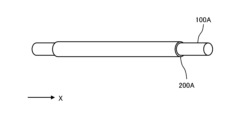
- FIG. 1 is a diagram for explaining a method for manufacturing an electroformed pipe according to Embodiment 1.
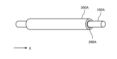
- FIG. 1 is a diagram for explaining a method for manufacturing an electroformed pipe according to Embodiment 1.
- FIG. 1 is a diagram for explaining a method for manufacturing an electroformed pipe according to Embodiment 1.
- FIG. 1 is a diagram for explaining a method for manufacturing an electroformed pipe according to Embodiment 1.
- FIG. 1 is a diagram for explaining a method for manufacturing an electroformed pipe according to Embodiment 1.
- FIG. 1 is a diagram for explaining a method for manufacturing an electroformed pipe according to Embodiment 1.
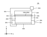
- FIG. 1 is a diagram showing an electroforming apparatus according to Embodiment 1.
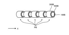
- FIG. 7 is a diagram for explaining a method for manufacturing an electroformed pipe according to a second embodiment.
- FIG. 7 is a diagram for explaining a method for manufacturing an electroformed pipe according to a second embodiment. It is a sectional view of the shaft material concerning a modification.
- (Embodiment 1) 1 to 6 are diagrams for explaining the method for manufacturing an electroformed tube according to the first embodiment.
- the electroformed tube according to the first embodiment can be used, for example, as a probe for testing an object to be tested such as an IC.
- the method for manufacturing an electroformed tube according to Embodiment 1 will be simply referred to as the method according to Embodiment 1.
- the X direction indicates the axial direction of the wire 100A, which will be described later.
- a wire rod 100A is prepared.
- the wire 100A has conductivity.
- the wire 100A is made of stainless steel, for example.
- the wire 100A may be made of a material different from stainless steel.
- the wire 100A may be made of iron, copper, gold, silver, brass, nickel, aluminum, carbon, plastic, resin, or the like.
- the wire 100A extends substantially parallel to the X direction.
- the cross section of the wire 100A perpendicular to the X direction has a substantially circular shape.
- the diameter of the wire 100A perpendicular to the X direction is, for example, 10 ⁇ m or more and 500 ⁇ m or less.
- a sacrificial layer 200A is formed around the outer peripheral surface of the wire 100A when viewed from the X direction, excluding both ends of the wire 100A in the X direction.
- the outer peripheral surface of the wire 100A is coated with the sacrificial layer 200A when viewed from the X direction, except for both ends of the wire 100A in the X direction.
- the sacrificial layer 200A is made of metal such as copper, for example.
- the sacrificial layer 200A may be made of a metal different from copper.
- the sacrificial layer 200A may be made of copper, gold, nickel, or the like.
- the sacrificial layer 200A is formed by, for example, electroplating, electroless plating, or the like.
- the thickness of the sacrificial layer 200A perpendicular to the X direction is, for example, 0.3 ⁇ m or more and 3 ⁇ m or less.
- an electroformed layer 300A is formed around the outer peripheral surface of the sacrificial layer 200A when viewed from the X direction, excluding both ends of the wire 100A in the X direction.
- a shaft member including the wire 100A, the sacrificial layer 200A, and the electroformed layer 300A is formed.
- the electroformed layer 300A is formed by electroforming using an electroforming apparatus 1A, which will be described later with reference to FIG.
- the electroformed layer 300A is made of, for example, metals such as nickel, gold, copper, palladium, rhodium, platinum, and silver, or alloys thereof.
- the thickness of the electroformed layer 300A perpendicular to the X direction is, for example, 5 ⁇ m or more and 100 ⁇ m or less.
- the sacrificial layer 200A located between the outer peripheral surface of the wire 100A and the inner peripheral surface of the electroformed layer 300A when viewed from the X direction is removed.
- a gap 400A is formed between the outer peripheral surface of the wire 100A and the inner peripheral surface of the electroformed layer 300A when viewed from the X direction.
- the sacrificial layer 200A is removed by etching such as wet etching.
- the sacrificial layer 200A may be removed by an etching method different from wet etching.
- the etching rate of the etchant used for etching with respect to the sacrificial layer 200A is higher than the etching rate of the etchant with respect to the electroformed layer 300A. That is, the etching rate of the metal constituting the sacrificial layer 200A is higher than the etching rate of the electroformed layer 300A. Therefore, the sacrificial layer 200A can be etched while the etching of the electroformed layer 300A is suppressed more than the etching of the sacrificial layer 200A.
- the entire sacrificial layer 200A does not need to be removed. That is, in the step shown in FIG. 4, at least a portion of the sacrificial layer 200A is removed so that a gap 400A is formed between the outer peripheral surface of the wire rod 100A and the inner peripheral surface of the electroformed layer 300A when viewed from the X direction. be able to.
- the sacrificial layer 200A may remain on at least a portion of the outer peripheral surface of the wire 100A when viewed from the X direction.
- the sacrificial layer 200A may remain on at least a portion of the inner peripheral surface of the electroformed layer 300A when viewed from the X direction. In this case, after removing the wire 100A from the electroformed layer 300A as described later, the sacrificial layer 200A can be removed, for example, by etching.
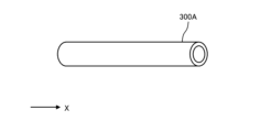
- the wire 100A is removed from the electroformed layer 300A.
- the wire 100A is removed from the electroformed layer 300A by pulling the wire 100A in the X direction from the electroformed layer 300A.
- the outer peripheral surface of the wire 100A and the inner peripheral surface of the electroformed layer 300A do not need to be pulled in the X direction at least one end of the wire 100A in the X direction.
- a gap 400A is formed between them.
- the gap 400A can suppress damage to the inner peripheral surface of the electroformed layer 300A due to the burr of the wire 100A or the displacement of the wire 100A. For example, even if at least one end of the wire rod 100A in the X direction is not pulled in the X direction, a sufficient gap can be secured between the outer peripheral surface of the wire rod 100A and the inner peripheral surface of the electroformed layer 300A when viewed from the X direction. . Alternatively, at least one end of the wire 100A in the X direction may be pulled in the X direction.
- the method for removing the wire 100A from the electroformed layer 300A is not limited to pulling the wire 100A from the electroformed layer 300A in the X direction.
- the wire 100A may be removed from the electroformed layer 300A by applying physical force such as ultrasound, water pressure, vibration, etc. to the wire 100A and the electroformed layer 300A.
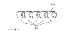
- the electroformed layer 300A is cut into a plurality of pieces PA.
- the electroformed layer 300A is schematically cut into five pieces PA lined up in the X direction.
- the length of each piece PA in the X direction is approximately equal. However, the lengths of at least some of the pieces PA in the X direction may be different from each other.
- Each piece PA cut out becomes an electroformed pipe. In this way, the electroformed tube according to Embodiment 1 is manufactured.
- the method for manufacturing the electroformed tube can be simplified.
- the combination of materials for the wire 100A, the sacrificial layer 200A, and the electroformed layer 300A is, for example, stainless steel for the wire 100A, copper for the sacrificial layer 200A, and nickel for the electroformed layer 300A.
- the combination of these materials is not limited to this example.
- the combination of these materials includes at least one selected from the group consisting of stainless steel, iron, copper, gold, silver, brass, nickel, aluminum, carbon, plastic, and resin per 100A of wire material, and copper, per sacrificial layer 200A.
- the method for manufacturing an electroformed pipe is not limited to the method according to Embodiment 1.
- the method according to Embodiment 1 includes the steps of preparing a wire 100A shown in FIG. 1, forming a sacrificial layer 200A shown in FIG. 2, and forming an electroformed layer 300A shown in FIG. We are prepared.
- the method for manufacturing an electroformed pipe may include a step of preparing in advance a wire 100A whose outer peripheral surface is covered with the sacrificial layer 200A and the electroformed layer 300A when viewed from the X direction. .
- FIG. 7 is a diagram showing an electroforming apparatus 1A according to the first embodiment.
- the Z direction is a direction parallel to the vertical direction.
- the X direction is one of the horizontal directions perpendicular to the Z direction.
- the Y direction is one of the horizontal directions perpendicular to the Z direction and the X direction.
- description will be made assuming that the X direction is the left-right direction, the Y direction is the front-back direction, and the Z direction is the up-down direction.
- the directions pointed by the arrows in the X direction and the Z direction are defined as the right direction and the upward direction, respectively.
- the white circle with an X indicating the Y direction indicates the front direction from the back of the page to the front.
- the electroforming apparatus 1A includes an electroforming tank 10A, an outer tank 12A, a cathode wiring 32A, a pair of cathode contacts 34A, an anode 40A, an anode wiring 42A, and a power source 50A.
- the electroforming tank 10A is housed inside the outer tank 12A.
- the upper end of the electroforming tank 10A and the upper end of the outer tank 12A are open upward.
- the electroforming liquid 20A is always supplied to the electroforming tank 10A.
- the electroforming liquid 20A overflows from the upper part of the electroforming tank 10A.
- the electroforming liquid 20A overflowing from the electroforming tank 10A flows into the outer tank 12A.
- the electroforming liquid 20A overflowing from the electroforming tank 10A and flowing into the outer tank 12A is again supplied to the electroforming tank 10A by a filtering device (not shown). In this way, during operation of the electroforming apparatus 1A, the electroforming liquid 20A circulates through the electroforming tank 10A, the outer tank 12A, and the filtration device.
- the type of electroforming liquid 20A is determined by predetermined conditions such as the material of the electroforming layer 300A formed on the outer peripheral surface of the wire 100A.
- the electroforming solution 20A includes, for example, a nickel sulfate solution or a nickel sulfamate solution, and optionally includes a brightening agent and a bit prevention agent.
- the wire rod 100A is impregnated in the electroforming solution 20A in the electroforming tank 10A.
- the longitudinal direction of the wire 100A is approximately parallel to the X direction.
- the outer peripheral surface of the wire 100A is covered with the sacrificial layer 200A when viewed from the X direction.
- Both ends of the wire 100A in the X direction are supported by a pair of cathode contacts 34A.
- Both ends of the wire 100A in the X direction are electrically connected to a power source 50A via a cathode wire 32A. Thereby, the wire 100A is operating as a cathode.
- the anode 40A is impregnated with the electroforming solution 20A in the electroforming tank 10A.
- the longitudinal direction of the anode 40A is approximately parallel to the X direction.
- the anode 40A is arranged below the wire 100A.
- Anode 40A is electrically connected to power supply 50A via anode wiring 42A.
- the electroformed layer 300A is formed around the outer peripheral surface of the sacrificial layer 200A when viewed from the X direction, as described using FIG. 3.
- (Embodiment 2) 8 and 9 are diagrams for explaining a method for manufacturing an electroformed pipe according to the second embodiment.
- the method for manufacturing an electroformed tube according to the second embodiment will be simply referred to as the method according to the second embodiment.
- the method according to the second embodiment is similar to the method according to the first embodiment except for the following points.
- the wire rod 100B is A sacrificial layer 200B and an electroformed layer 300B are sequentially formed around the outer peripheral surface of the wire 100B.
- a shaft member including the wire rod 100B, the sacrificial layer 200B, and the electroformed layer 300B is formed.
- the wire 100B, the sacrificial layer 200B, and the electroformed layer 300B are integrally cut into a plurality of pieces PB.
- the wire 100B, the sacrificial layer 200B, and the electroformed layer 300B are schematically cut into five pieces PB lined up in the X direction.
- Each piece PB includes a wire 100B, a sacrificial layer 200B, and an electroformed layer 300B.
- the sacrificial layer 200B of each piece PB is removed.
- a gap 400B is formed between the outer circumferential surface of the wire rod 100B of each piece PB and the inner circumferential surface of the electroformed layer 300B when viewed from the X direction.
- the sacrificial layer 200B of each piece PB is removed by etching such as wet etching.
- the sacrificial layer 200B of each piece PB may be removed by etching different from wet etching.
- the length of the sacrificial layer 200B of each piece PB according to the second embodiment in the X direction is shorter than the length of the sacrificial layer 200A according to the first embodiment in the X direction. Therefore, in Embodiment 2, compared to Embodiment 1, it is easier for an etchant such as an etching solution to penetrate between the outer circumferential surface of the wire rod 100B and the inner circumferential surface of the electroformed layer 300B when viewed from the X direction. . Therefore, in the second embodiment, the sacrificial layer 200B of each piece PB can be etched in a shorter time than in the first embodiment. Furthermore, in the second embodiment, compared to the first embodiment, etching of the electroformed layer 300B of each piece PB can be suppressed by etching the sacrificial layer 200B of each piece PB for a short time.
- an etchant such as an etching solution
- each piece PB from which the wire rod 100B has been removed becomes an electroformed tube.
- the wire rod 100B of each piece PB is removed from the electroformed layer 300B by physical force such as ultrasound, water pressure, vibration, etc., for example.
- the length in the X direction of the wire rod 100B of each piece PB according to the second embodiment is shorter than the length in the X direction of the wire rod 100A according to the first embodiment. Therefore, in the second embodiment, compared to the first embodiment, the wire rod 100B of each piece PB can be easily removed.
- the method for manufacturing an electroformed pipe is not limited to the method according to the second embodiment.
- the length of each piece PB in the X direction is It is approximately equal to the length in the X direction of the electroformed tube to be finally manufactured.
- the length of each piece PB in the X direction in the process shown in FIG. 8 does not have to be equal to the length of the finally manufactured electroformed tube in the X direction.
- the electroformed layer 300B of each piece PB may be cut into a predetermined length to manufacture an electroformed pipe.
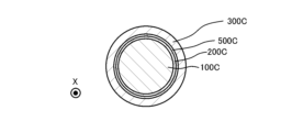
- FIG. 10 is a cross-sectional view of a shaft member according to a modification.
- a white circle with a black dot indicating the X direction indicates that the tip of the arrow indicating the X direction is directed from the back of the page to the front.
- the shaft member according to the modified example is the same as the shaft member according to Embodiment 1 or Embodiment 2, except for the following points.
- the shaft material according to the modification includes a wire 100C, a sacrificial layer 200C, a conductive layer 500C, and an electroformed layer 300C.
- the outer peripheral surface of the wire 100C is covered with a sacrificial layer 200C.
- the conductive layer 500C is located between the outer peripheral surface of the sacrificial layer 200C and the inner peripheral surface of the electroformed layer 300C.
- the conductive layer 500C is made of, for example, a different material from the material that constitutes the electroformed layer 300C.
- As the material of the conductive layer 500C for example, a material that is compatible with the material of the electroformed layer 300C is used.
- the conductive layer 500C is, for example, a metal plating layer such as a gold plating layer. Alternatively, the conductive layer 500C may be made of a metal different from gold, such as silver, iron, copper, or aluminum.
- the conductive layer 500C is formed on the outer peripheral surface of the sacrificial layer 200C by, for example, plating after the sacrificial layer 200C is formed on the outer peripheral surface of the wire 100C. Next, by forming an electroformed layer 300C on the outer circumferential surface of the conductive layer 500C, a shaft member according to the modified example is formed.
- a gap can be formed between the outer peripheral surface of the wire 100C and the inner peripheral surface of the conductive layer 500C when viewed from the X direction. Therefore, similarly to Embodiment 1 or Embodiment 2, the wire 100C can be easily removed.
- the conductive layer 500C can be left on the inner peripheral surface of the electroformed layer 300C.
- the conductivity of the electroformed pipe obtained from the electroformed layer 300C can be improved compared to the case where the conductive layer 500C is not provided on the inner peripheral surface of the electroformed layer 300C.
- the combination of materials for the wire 100C, the sacrificial layer 200C, the electroformed layer 300C, and the conductive layer 500C is not particularly limited.
- the materials of the wire 100C, the sacrificial layer 200C, the electroformed layer 300C, and the conductive layer 500C may be the same or different, or two or more may be the same.
- the combination of these materials includes at least one selected from the group consisting of stainless steel, iron, copper, gold, silver, brass, nickel, aluminum, carbon, plastic, and resin per 100C of wire material, and copper, per sacrificial layer 200C.
- the combination of these materials can be determined such that, for example, in the process of removing the sacrificial layer 200C by etching, the sacrificial layer 200C is etched more selectively than the electroformed layer 300A and the conductive layer 500C.
- the etching rate of the etchant used for etching the sacrificial layer 200C for the electroformed layer 300C and the conductive layer 500C is lower than the etching rate of the etchant for the sacrificial layer 200C.
- the electroformed layer may not be a single layer but multiple layers.
- the method for removing the sacrificial layer is not limited to etching.
- the sacrificial layer may be made of resin.
- the sacrificial layer can be removed by dissolving the sacrificial layer with a predetermined chemical solution.
- the shaft material includes a wire, an electroformed layer located around the wire, and a sacrificial layer located between the wire and the electroformed layer.
- the sacrificial layer can be removed by a predetermined method.
- a gap can be formed between the wire and the electroformed layer. Therefore, in the above-mentioned aspect, the wire can be easily removed from the electroformed layer.
- the etching rate of the sacrificial layer is higher than the etching rate of the electroformed layer.
- the sacrificial layer can be etched more selectively than the electroformed layer by predetermined etching. Therefore, by selectively etching the sacrificial layer, a gap can be formed between the wire and the electroformed layer.
- the shaft member further includes a conductive layer located between the sacrificial layer and the electroformed layer.
- the conductive layer can be left on the electroformed layer after the wire is removed.
- the conductivity of the electroformed tube obtained from the electroformed layer can be improved compared to the case where the electroformed layer is not provided with a conductive layer.
- the method for manufacturing an electroformed tube includes the step of removing the wire after removing at least a portion of a sacrificial layer located between a wire and an electroformed layer located around the wire. ing.
- a gap can be formed between the wire and the electroformed layer by removing the sacrificial layer. Therefore, in the above-mentioned aspect, the wire can be easily removed from the electroformed layer.
- the method for manufacturing an electroformed tube further includes the step of cutting the electroformed layer into a plurality of pieces after removing the wire rod.
- the method for manufacturing an electroformed tube further includes the step of integrally cutting the wire, the sacrificial layer, and the electroformed layer into a plurality of pieces, and in the step of removing the wire, the After removing at least a portion of the sacrificial layer, the wire of each piece is removed.
- the sacrificial layer of each piece can be etched in a shorter time than in the case described above. Furthermore, compared to the above case, etching of the electroformed layer of each piece can be suppressed by etching the sacrificial layer of each piece for a short time. Furthermore, compared to the case described above, each piece of wire can be easily removed.
- a conductive layer is disposed between the sacrificial layer and the electroformed layer.
- the conductive layer can be left on the electroformed layer after the wire is removed.
- the electrical conductivity of the electroformed tube can be improved compared to the case where the electroformed layer is not provided with a conductive layer.
- 1A electroforming device 10A electroforming tank, 12A outer tank, 20A electroforming solution, 32A cathode wiring, 34A cathode contact, 40A anode, 42A anode wiring, 50A power supply, 100A, 100B, 100C wire rod, 200A, 200B, 200C Sacrifice Layer, 300A, 300B, 300C Electroformed layer, 400A, 400B Gap, 500C Conductive layer, PA, PB piece
Landscapes
- Chemical & Material Sciences (AREA)
- Organic Chemistry (AREA)
- Chemical Kinetics & Catalysis (AREA)
- Electrochemistry (AREA)
- Materials Engineering (AREA)
- Metallurgy (AREA)
- Engineering & Computer Science (AREA)
- Micromachines (AREA)
- Flexible Shafts (AREA)
- Manufacturing Of Electrical Connectors (AREA)
- Shafts, Cranks, Connecting Bars, And Related Bearings (AREA)
- Forging (AREA)
- Golf Clubs (AREA)
Abstract
線材と、前記線材の周囲に位置する電鋳層と、前記線材と前記電鋳層との間に位置する犠牲層と、を備える軸材。
Description
本発明は、軸材及び電鋳管の製造方法に関する。
近年、電鋳管を製造するための様々な方法が開発されている。電鋳管は、例えば、集積回路(IC)等の検査対象物を検査するためのプローブに用いられている。例えば、特許文献1に記載の方法では、金めっきによって被膜されたステンレス製の線材の周囲に電鋳によってニッケル層を形成する。次いで、線材の少なくとも一端を引っ張ることで、線材の断面積を低減させて、線材の外周面とニッケル層の内周面との間に隙間を形成する。次いで、当該隙間が形成された状態で線材を引っ張ることで線材を除去する。
例えば特許文献1に記載の方法では、線材の引っ張りによる線材の破断を抑制する観点から、線材を一定の長さ以上に引っ張ることが難しいことがある。このため、線材の少なくとも一端を引っ張っても、線材の外周面と電鋳層の内周面との間に十分な隙間を形成することが難しいことがある。この場合、電鋳層から線材が除去しにくいことがある。
本発明の目的の一例は、電鋳層から線材を除去しやすくすることにある。本発明の他の目的は、本明細書の記載から明らかになるであろう。
本発明の一態様は、
線材と、
前記線材の周囲に位置する電鋳層と、
前記線材と前記電鋳層との間に位置する犠牲層と、
を備える軸材である。
線材と、
前記線材の周囲に位置する電鋳層と、
前記線材と前記電鋳層との間に位置する犠牲層と、
を備える軸材である。
本発明の一態様は、
線材と、前記線材の周囲に位置する電鋳層と、の間に位置する犠牲層の少なくとも一部分を除去した後、前記線材を除去する工程を備える、電鋳管の製造方法である。
線材と、前記線材の周囲に位置する電鋳層と、の間に位置する犠牲層の少なくとも一部分を除去した後、前記線材を除去する工程を備える、電鋳管の製造方法である。
本発明の上記態様によれば、電鋳層から線材を除去しやすくすることができる。
以下、本発明の実施形態及び変形例について、図面を用いて説明する。すべての図面において、同様な構成要素には同様の符号を付し、適宜説明を省略する。
(実施形態1)
図1~図6は、実施形態1に係る電鋳管の製造方法を説明するための図である。実施形態1に係る電鋳管は、例えば、IC等の検査対象物を検査するためのプローブに利用可能である。以下、実施形態1に係る電鋳管の製造方法を、単に、実施形態1に係る方法という。
図1~図6は、実施形態1に係る電鋳管の製造方法を説明するための図である。実施形態1に係る電鋳管は、例えば、IC等の検査対象物を検査するためのプローブに利用可能である。以下、実施形態1に係る電鋳管の製造方法を、単に、実施形態1に係る方法という。
図1~図6における方向を説明するために、X方向を定義する。X方向は、後述する線材100Aの軸方向を示している。
図1~図6を参照して、実施形態1に係る方法を説明する。
まず、図1に示すように、線材100Aを準備する。線材100Aは、導電性を有している。線材100Aは、例えば、ステンレス製である。ただし、線材100Aは、ステンレスと異なる材料からなっていてもよい。例えば、線材100Aは、鉄、銅、金、銀、真鍮、ニッケル、アルミニウム、カーボン、プラスチック、樹脂等からなっていてもよい。線材100Aは、X方向に略平行に延在している。線材100AのX方向に垂直な断面は、略円形状となっている。線材100AのX方向に垂直な直径は、例えば、10μm以上500μm以下である。
次いで、図2に示すように、線材100AのX方向の両端部を除いて、X方向から見て線材100Aの外周面の周囲に犠牲層200Aを形成する。これによって、線材100AのX方向の両端部を除いて、X方向から見て線材100Aの外周面が犠牲層200Aによって被膜される。犠牲層200Aは、例えば、銅等の金属からなっている。ただし、犠牲層200Aは、銅と異なる金属からなっていてもよい。例えば、犠牲層200Aは、銅、金、ニッケル等からなっていてもよい。犠牲層200Aは、例えば、電解めっき、無電解めっき等のめっきによって形成されている。犠牲層200AのX方向に垂直な厚さは、例えば、0.3μm以上3μm以下である。
次いで、図3に示すように、線材100AのX方向の両端部を除いて、X方向から見て犠牲層200Aの外周面の周囲に電鋳層300Aを形成する。これによって、線材100A、犠牲層200A及び電鋳層300Aを備える軸材が形成される。電鋳層300Aは、後述する図7を参照して説明する電鋳装置1Aを用いた電鋳によって形成されている。電鋳層300Aは、例えば、ニッケル、金、銅、パラジウム、ロジウム、白金、銀等の金属やこれらの合金からなっている。電鋳層300AのX方向に垂直な厚さは、例えば、5μm以上100μm以下である。
次いで、図4に示すように、X方向から見て線材100Aの外周面と電鋳層300Aの内周面との間に位置する犠牲層200Aを除去する。これによって、X方向から見て線材100Aの外周面と電鋳層300Aの内周面との間に隙間400Aが形成される。犠牲層200Aは、例えばウエットエッチング等のエッチングによって除去される。ただし、犠牲層200Aは、ウエットエッチングと異なるエッチングによって除去されてもよい。この例において、エッチングに用いられるエッチャントの犠牲層200Aに対するエッチングレートは、当該エッチャントの電鋳層300Aに対するエッチングレートより高くなっている。すなわち、犠牲層200Aを構成する金属のエッチングレートは、電鋳層300Aのエッチングレートより高くなっている。したがって、電鋳層300Aのエッチングを犠牲層200Aのエッチングより抑えた状態で、犠牲層200Aをエッチングすることができる。
図4に示す工程では、犠牲層200Aのすべてが除去されていなくてもよい。すなわち、図4に示す工程では、X方向から見て線材100Aの外周面と電鋳層300Aの内周面との間に隙間400Aが形成されるように、犠牲層200Aの少なくとも一部分を除去することができる。例えば、X方向から見て線材100Aの外周面の少なくとも一部分に犠牲層200Aが残っていてもよい。この場合、X方向から見て電鋳層300Aの内周面に犠牲層200Aが残っていなければ、電鋳層300Aから得られる電鋳管が犠牲層200Aの影響を受けないようにすることができる。或いは、X方向から見て電鋳層300Aの内周面の少なくとも一部分に犠牲層200Aが残っていてもよい。この場合、後述するように電鋳層300Aから線材100Aを除去した後に、当該犠牲層200Aを例えばエッチングによって除去することができる。
次いで、図5に示すように、電鋳層300Aから線材100Aを除去する。例えば、電鋳層300Aから線材100AをX方向に引き抜くことで、電鋳層300Aから線材100Aが除去されている。図4を用いて説明したように、実施形態1に係る方法では、線材100AのX方向の少なくとも一端をX方向に引っ張らなくとも、線材100Aの外周面と電鋳層300Aの内周面との間に隙間400Aが形成されている。線材100Aの外周面にはバリが存在したり、線材100Aの電鋳層300Aからの除去時に線材100AのX方向からのずれが生じたりすることがある。実施形態1に係る方法では、線材100Aの当該バリや線材100Aの当該ずれによる電鋳層300Aの内周面の傷を隙間400Aによって抑制することができる。例えば、線材100AのX方向の少なくとも一端をX方向に引っ張らなくとも、X方向から見て線材100Aの外周面と電鋳層300Aの内周面との間に十分な隙間を確保することができる。或いは、線材100AのX方向の少なくとも一端をX方向に引っ張ってもよい。この場合、線材100AのX方向に引っ張られる長さが比較的短くても、X方向から見て線材100Aの外周面と電鋳層300Aの内周面との間に十分な隙間を確保することができる。
電鋳層300Aから線材100Aを除去する方法は、電鋳層300Aから線材100AをX方向に引き抜くことに限定されない。例えば、超音波、水圧、振動等の物理的な力を線材100A及び電鋳層300Aに与えることで、電鋳層300Aから線材100Aを除去してもよい。
次いで、図6に示すように、電鋳層300Aを複数の片PAに切断する。図6に示す例では、電鋳層300Aは、X方向に並ぶ5つの片PAに模式的に切断されている。各片PAのX方向の長さは、略等しくなっている。ただし、少なくとも一部の片PAのX方向の長さは、互いに異なっていてもよい。切り出された各片PAは電鋳管となる。これによって、実施形態1に係る電鋳管が製造される。
実施形態1では、線材100Aを複数の片に切断する必要がない。したがって、線材100Aを複数の片に切断する場合と比較して、電鋳管の製造方法を簡易にすることができる。
線材100A、犠牲層200A及び電鋳層300Aの各々の材料の組み合わせは、例えば、線材100Aにつきステンレス、犠牲層200Aにつき銅、電鋳層300Aにつきニッケルである。ただし、これらの材料の組み合わせは、当該例に限定されない。例えば、これらの材料の組み合わせは、線材100Aにつきステンレス、鉄、銅、金、銀、真鍮、ニッケル、アルミニウム、カーボン、プラスチック及び樹脂からなる群から選択される少なくとも1つと、犠牲層200Aにつき銅、金及びニッケルからなる群から選択される少なくとも1つと、電鋳層300Aにつきニッケル、金、銅、パラジウム、ロジウム、白金、銀及びこれらの合金からなる群から選択される少なくとも1つと、の組み合わせである。また、これらの材料組み合わせは、例えば、犠牲層200Aをエッチングによって除去する工程において犠牲層200Aが電鋳層300Aよりも選択的にエッチングされるように決定することができる。
電鋳管の製造方法は、実施形態1に係る方法に限定されない。例えば、実施形態1に係る方法は、図1に示す線材100Aを準備する工程と、図2に示す犠牲層200Aを形成する工程と、図3に示す電鋳層300Aを形成する工程と、を備えている。しかしながら、電鋳管の製造方法は、これらの工程に代えて、X方向から見て外周面が犠牲層200A及び電鋳層300Aによって覆われた線材100Aを予め準備する工程を備えていてもよい。
図7は、実施形態1に係る電鋳装置1Aを示す図である。
図7における方向を説明するために、X方向、Y方向及びZ方向を定義する。Z方向は、鉛直方向に平行な方向である。X方向は、Z方向に垂直な水平方向の一つである。Y方向は、Z方向及びX方向に垂直な水平方向の一つである。図7では、X方向が左右方向、Y方向が前後方向、Z方向が上下方向であるとして説明する。図7では、X方向及びZ方向の各々の矢印が指し示す方向をそれぞれ右方向及び上方向と定義する。図7では、Y方向を示すX付き白丸は、紙面の奥から手前に向けて前方向であることを示している。
実施形態1に係る電鋳装置1Aは、電鋳槽10A、外槽12A、陰極配線32A、一対の陰極接点34A、陽極40A、陽極配線42A及び電源50Aを備えている。
電鋳槽10Aは、外槽12Aの内部に収容されている。電鋳槽10Aの上端及び外槽12Aの上端は、上方に向けて開口している。電鋳装置1Aの運転時において、電鋳槽10Aには、常時、電鋳液20Aが供給されている。これによって、電鋳槽10Aの上部から電鋳液20Aが溢れ出している。電鋳槽10Aから溢れ出した電鋳液20Aは、外槽12Aに流れ込んでいる。電鋳槽10Aから溢れ出して外槽12Aに流れ込んだ電鋳液20Aは、不図示のろ過装置によって電鋳槽10Aに再び供給されている。このようにして、電鋳装置1Aの運転時において、電鋳液20Aは、電鋳槽10A、外槽12A及びろ過装置を循環している。
電鋳液20Aの種類は、線材100Aの外周面に形成される電鋳層300Aの材料等の所定の条件によって決定されている。電鋳液20Aは、例えば、硫酸ニッケル液又はスルファミン酸ニッケル液を含み、光沢剤及びビット防止剤を必要に応じて含んでいる。
電鋳槽10A内の電鋳液20Aには、線材100Aが含浸されている。実施形態1において、線材100Aの長手方向は、X方向に略平行となっている。図2を用いて説明したように、実施形態1では、X方向から見て、線材100Aの外周面は、犠牲層200Aによって覆われている。線材100AのX方向の両端部は、一対の陰極接点34Aによって支持されている。線材100AのX方向の両端部は、陰極配線32Aを介して電源50Aに電気的に接続されている。これによって、線材100Aは、陰極として動作している。
陽極40Aは、電鋳槽10A内の電鋳液20Aに含浸されている。実施形態1において、陽極40Aの長手方向は、X方向に略平行となっている。陽極40Aは、線材100Aの下方に配置されている。陽極40Aは、陽極配線42Aを介して電源50Aに電気的に接続されている。
電源50Aによって線材100A及び陽極40Aに電力が供給されることで、図3を用いて説明したように、X方向から見て犠牲層200Aの外周面の周囲に電鋳層300Aが形成される。
(実施形態2)
図8及び図9は、実施形態2に係る電鋳管の製造方法を説明するための図である。以下、実施形態2に係る電鋳管の製造方法を、単に、実施形態2に係る方法という。実施形態2に係る方法は、以下の点を除いて、実施形態1に係る方法と同様である。
図8及び図9は、実施形態2に係る電鋳管の製造方法を説明するための図である。以下、実施形態2に係る電鋳管の製造方法を、単に、実施形態2に係る方法という。実施形態2に係る方法は、以下の点を除いて、実施形態1に係る方法と同様である。
実施形態1の図1~図3と、実施形態2の図8及び図9と、を参照して、実施形態2に係る方法を説明する。
実施形態2に係る方法では、まず、実施形態1に係る方法と同様にして、図1~図3を用いて説明したように、線材100BのX方向の両端を除いて、X方向から見て線材100Bの外周面の周囲に犠牲層200B及び電鋳層300Bを順に形成する。これによって、線材100B、犠牲層200B及び電鋳層300Bを備える軸材が形成される。
次いで、図8に示すように、線材100B、犠牲層200B及び電鋳層300Bを一体的に複数の片PBに切断する。図8に示す例では、線材100B、犠牲層200B及び電鋳層300Bは、X方向に並ぶ5つの片PBに模式的に切断されている。各片PBは、線材100B、犠牲層200B及び電鋳層300Bを有している。
次いで、図9に示すように、各片PBの犠牲層200Bの少なくとも一部分を除去する。これによって、X方向から見て各片PBの線材100Bの外周面と電鋳層300Bの内周面との間に隙間400Bが形成される。各片PBの犠牲層200Bは、例えばウエットエッチング等のエッチングによって除去される。ただし、各片PBの犠牲層200Bは、ウエットエッチングと異なるエッチングによって除去されてもよい。実施形態2に係る各片PBの犠牲層200BのX方向の長さは、実施形態1に係る犠牲層200AのX方向の長さより短くなっている。したがって、実施形態2では、実施形態1と比較して、X方向から見て線材100Bの外周面と電鋳層300Bの内周面との間にエッチング液等のエッチャントを浸透させやすくなっている。このため、実施形態2では、実施形態1と比較して、各片PBの犠牲層200Bを短時間でエッチングすることができる。さらに、実施形態2では、実施形態1と比較して、各片PBの犠牲層200Bの短時間のエッチングによって各片PBの電鋳層300Bのエッチングを抑制することができる。
次いで、各片PBの線材100Bを除去する。線材100Bが除去された各片PBは、電鋳管となる。各片PBの線材100Bは、例えば、超音波、水圧、振動等の物理的な力によって電鋳層300Bから除去される。実施形態2に係る各片PBの線材100BのX方向の長さは、実施形態1に係る線材100AのX方向の長さより短くなっている。したがって、実施形態2では、実施形態1と比較して、各片PBの線材100Bの除去を容易にすることができる。
電鋳管の製造方法は、実施形態2に係る方法に限定されない。例えば、実施形態2に係る方法では、図8に示す線材100B、犠牲層200B及び電鋳層300Bを一体的に複数の片PBに切断する工程において、各片PBのX方向の長さは、最終的に製造される電鋳管のX方向の長さと略等しくなっている。しかしながら、図8に示す工程における各片PBのX方向の長さは、最終的に製造される電鋳管のX方向の長さと等しくしなくてもよい。例えば、図8に示す工程における各片PBのX方向の長さは、最終的に製造される電鋳管のX方向の長さより長くてもよい。この場合、各片PBの線材100Bを除去した後、各片PBの電鋳層300Bを所定の長さに切断して電鋳管を製造してもよい。
図10は、変形例に係る軸材の断面図である。図10において、X方向を示す黒点付き白丸は、X方向を示す矢印の先端が紙面の奥から手前に向かう方向に向けられていることを示している。変形例に係る軸材は、以下の点を除いて、実施形態1又は実施形態2に係る軸材と同様である。
変形例に係る軸材は、線材100C、犠牲層200C、導電層500C及び電鋳層300Cを備えている。X方向から見て、線材100Cの外周面は、犠牲層200Cによって覆われている。X方向から見て、導電層500Cは、犠牲層200Cの外周面と電鋳層300Cの内周面との間に位置している。導電層500Cは、例えば、電鋳層300Cを構成する材料と異なる材料によって形成されている。導電層500Cの材料としては、例えば、電鋳層300Cの材料と親和性がある材料が用いられる。導電層500Cは、例えば、金めっき層等の、金属めっき層である。或いは、導電層500Cは、例えば、銀、鉄、銅、アルミニウム等の、金と異なる金属であってもよい。導電層500Cは、線材100Cの外周面に犠牲層200Cが形成された後、例えば、めっきによって犠牲層200Cの外周面に形成されている。次いで、導電層500Cの外周面に電鋳層300Cを形成することで、変形例に係る軸材が形成される。
変形例に係る軸材においても、犠牲層200Cを除去することで、X方向から見て線材100Cの外周面と導電層500Cの内周面との間に隙間を形成することができる。したがって、実施形態1又は実施形態2と同様にして、線材100Cの除去を容易にすることができる。
変形例に係る軸材においては、線材100Cを除去した後、電鋳層300Cの内周面に導電層500Cを残すことができる。この場合、電鋳層300Cの内周面に導電層500Cが設けられていない場合と比較して、電鋳層300Cから得られる電鋳管の導電率を向上させることができる。
線材100C、犠牲層200C、電鋳層300C及び導電層500Cの各々の材料の組み合わせは、特に限定されない。線材100C、犠牲層200C、電鋳層300C及び導電層500Cの各々の材料は同じであってもいいし、違っていてもよいし、2つ以上が同じであってもよい。例えば、これらの材料の組み合わせは、線材100Cにつきステンレス、鉄、銅、金、銀、真鍮、ニッケル、アルミニウム、カーボン、プラスチック及び樹脂からなる群から選択される少なくとも1つと、犠牲層200Cにつき銅、金及びニッケルからなる群から選択される少なくとも1つと、電鋳層300Cにつきニッケル、金、銅、パラジウム、ロジウム、白金、銀及びこれらの合金からなる群から選択される少なくとも1つと、導電層500Cにつき金、銀、鉄、銅及びアルミニウムからなる群から選択される少なくとも1つと、の組み合わせである。また、これらの材料の組み合わせは、例えば、犠牲層200Cをエッチングによって除去する工程において、犠牲層200Cが電鋳層300A及び導電層500Cよりも選択的にエッチングされるように決定することができる。例えば、犠牲層200Cのエッチングに用いられるエッチャントの電鋳層300C及び導電層500Cに対するエッチングレートは、当該エッチャントの犠牲層200Cに対するエッチングレートより低くなっている。
以上、図面を参照して本発明の実施形態及び変形例について述べたが、これらは本発明の例示であり、上記以外の様々な構成を採用することもできる。
例えば、電鋳層は、単層ではなく、複数層であってもよい。
また、犠牲層の除去方法は、エッチングに限定されない。例えば、犠牲層は樹脂からなっていてもよい。この例では、所定の薬液によって犠牲層を溶かすことで犠牲層を除去することができる。
本明細書によれば、以下の態様の軸材及び電鋳管の製造方法が提供される。
(態様1)
態様1では、軸材が、線材と、前記線材の周囲に位置する電鋳層と、前記線材と前記電鋳層との間に位置する犠牲層と、を備えている。
(態様1)
態様1では、軸材が、線材と、前記線材の周囲に位置する電鋳層と、前記線材と前記電鋳層との間に位置する犠牲層と、を備えている。
上述の態様によれば、所定の方法によって、犠牲層を除去することができる。犠牲層の除去によって、線材と電鋳層との間に隙間を形成することができる。したがって、上述の態様では、電鋳層から線材を除去しやすくすることができる。
(態様2)
態様2では、前記犠牲層のエッチングレートが前記電鋳層のエッチングレートより高くなっている。
態様2では、前記犠牲層のエッチングレートが前記電鋳層のエッチングレートより高くなっている。
上述の態様によれば、所定のエッチングによって、犠牲層を電鋳層よりも選択的にエッチングすることができる。したがって、犠牲層の選択的なエッチングによって、線材と電鋳層との間に隙間を形成することができる。
(態様3)
態様3では、軸材が、前記犠牲層と前記電鋳層との間に位置する導電層をさらに備えている。
態様3では、軸材が、前記犠牲層と前記電鋳層との間に位置する導電層をさらに備えている。
上述の態様によれば、線材を除去した後、電鋳層に導電層を残すことができる。この場合、電鋳層に導電層が設けられていない場合と比較して、電鋳層から得られる電鋳管の導電率を向上させることができる。
(態様4)
態様4では、電鋳管の製造方法が、線材と、前記線材の周囲に位置する電鋳層と、の間に位置する犠牲層の少なくとも一部分を除去した後、前記線材を除去する工程を備えている。
態様4では、電鋳管の製造方法が、線材と、前記線材の周囲に位置する電鋳層と、の間に位置する犠牲層の少なくとも一部分を除去した後、前記線材を除去する工程を備えている。
上述の態様によれば、犠牲層の除去によって、線材と電鋳層との間に隙間を形成することができる。したがって、上述の態様では、電鋳層から線材を除去しやすくすることができる。
(態様5)
態様5では、電鋳管の製造方法が、前記線材を除去した後、前記電鋳層を複数の片に切断する工程をさらに備えている。
態様5では、電鋳管の製造方法が、前記線材を除去した後、前記電鋳層を複数の片に切断する工程をさらに備えている。
上述の態様によれば、線材を複数の片に切断する必要がない。したがって、線材を複数の片に切断する場合と比較して、電鋳管の製造方法を簡易にすることができる。
(態様6)
態様6では、電鋳管の製造方法が、前記線材、前記犠牲層及び前記電鋳層を一体的に複数の片に切断する工程をさらに備え、前記線材を除去する工程において、各片の前記犠牲層の少なくとも一部分を除去した後、各片の前記線材を除去している。
態様6では、電鋳管の製造方法が、前記線材、前記犠牲層及び前記電鋳層を一体的に複数の片に切断する工程をさらに備え、前記線材を除去する工程において、各片の前記犠牲層の少なくとも一部分を除去した後、各片の前記線材を除去している。
上述の態様によれば、線材、犠牲層及び電鋳層が一体的に複数の片に切断されていない場合と比較して、線材と電鋳層との間にエッチング液等のエッチャントを浸透させやすくなっている。このため、上述の場合と比較して、各片の犠牲層を短時間でエッチングすることができる。さらに、上述の場合と比較して、各片の犠牲層の短時間のエッチングによって各片の電鋳層のエッチングを抑制することができる。さらに、上述の場合と比較して、各片の線材の除去を容易にすることができる。
(態様7)
態様7では、前記犠牲層と前記電鋳層との間に導電層が配置されている。
態様7では、前記犠牲層と前記電鋳層との間に導電層が配置されている。
上述の態様によれば、線材を除去した後、電鋳層に導電層を残すことができる。この場合、電鋳層に導電層が設けられていない場合と比較して、電鋳管の導電率を向上させることができる。
この出願は、2022年4月27日に出願された日本出願特願2022-073118号を基礎とする優先権を主張し、その開示の全てをここに取り込む。
1A 電鋳装置、10A 電鋳槽、12A 外槽、20A 電鋳液、32A 陰極配線、34A 陰極接点、40A 陽極、42A 陽極配線、50A 電源、100A,100B,100C 線材、200A,200B,200C 犠牲層、300A,300B,300C 電鋳層、400A,400B 隙間、500C 導電層、PA,PB 片
Claims (7)
- 線材と、
前記線材の周囲に位置する電鋳層と、
前記線材と前記電鋳層との間に位置する犠牲層と、
を備える軸材。 - 前記犠牲層のエッチングレートが前記電鋳層のエッチングレートより高い、請求項1に記載の軸材。
- 前記犠牲層と前記電鋳層との間に位置する導電層をさらに備える、請求項1又は2に記載の軸材。
- 線材と、前記線材の周囲に位置する電鋳層と、の間に位置する犠牲層の少なくとも一部分を除去した後、前記線材を除去する工程を備える、電鋳管の製造方法。
- 前記線材を除去した後、前記電鋳層を複数の片に切断する工程をさらに備える、請求項4に記載の電鋳管の製造方法。
- 前記線材、前記犠牲層及び前記電鋳層を一体的に複数の片に切断する工程をさらに備え、
前記線材を除去する工程において、各片の前記犠牲層の少なくとも一部分を除去した後、各片の前記線材を除去する、請求項4に記載の電鋳管の製造方法。 - 前記犠牲層と前記電鋳層との間に導電層が配置されている、請求項4~6のいずれか一項に記載の電鋳管の製造方法。
Applications Claiming Priority (2)
| Application Number | Priority Date | Filing Date | Title |
|---|---|---|---|
| JP2022-073118 | 2022-04-27 | ||
| JP2022073118A JP2023162643A (ja) | 2022-04-27 | 2022-04-27 | 軸材及び電鋳管の製造方法 |
Publications (1)
| Publication Number | Publication Date |
|---|---|
| WO2023210458A1 true WO2023210458A1 (ja) | 2023-11-02 |
Family
ID=88518641
Family Applications (1)
| Application Number | Title | Priority Date | Filing Date |
|---|---|---|---|
| PCT/JP2023/015561 Ceased WO2023210458A1 (ja) | 2022-04-27 | 2023-04-19 | 軸材及び電鋳管の製造方法 |
Country Status (3)
| Country | Link |
|---|---|
| JP (1) | JP2023162643A (ja) |
| TW (1) | TW202409350A (ja) |
| WO (1) | WO2023210458A1 (ja) |
Citations (5)
| Publication number | Priority date | Publication date | Assignee | Title |
|---|---|---|---|---|
| JPS4953540A (ja) * | 1972-09-28 | 1974-05-24 | ||
| JPS62103386A (ja) * | 1985-10-24 | 1987-05-13 | ゼロツクス コ−ポレ−シヨン | 電鋳方法 |
| JP2002178027A (ja) * | 1992-11-16 | 2002-06-25 | Ir Internatl Inc | 機械彫刻した継目なし管の製造方法 |
| JP2002256475A (ja) * | 2001-03-06 | 2002-09-11 | Sumitomo Metal Mining Co Ltd | シームレスパイプの製造方法 |
| JP2016166783A (ja) * | 2015-03-09 | 2016-09-15 | 日本電子材料株式会社 | プローブ及びその製造方法 |
-
2022
- 2022-04-27 JP JP2022073118A patent/JP2023162643A/ja active Pending
-
2023
- 2023-04-19 TW TW112114594A patent/TW202409350A/zh unknown
- 2023-04-19 WO PCT/JP2023/015561 patent/WO2023210458A1/ja not_active Ceased
Patent Citations (5)
| Publication number | Priority date | Publication date | Assignee | Title |
|---|---|---|---|---|
| JPS4953540A (ja) * | 1972-09-28 | 1974-05-24 | ||
| JPS62103386A (ja) * | 1985-10-24 | 1987-05-13 | ゼロツクス コ−ポレ−シヨン | 電鋳方法 |
| JP2002178027A (ja) * | 1992-11-16 | 2002-06-25 | Ir Internatl Inc | 機械彫刻した継目なし管の製造方法 |
| JP2002256475A (ja) * | 2001-03-06 | 2002-09-11 | Sumitomo Metal Mining Co Ltd | シームレスパイプの製造方法 |
| JP2016166783A (ja) * | 2015-03-09 | 2016-09-15 | 日本電子材料株式会社 | プローブ及びその製造方法 |
Also Published As
| Publication number | Publication date |
|---|---|
| TW202409350A (zh) | 2024-03-01 |
| JP2023162643A (ja) | 2023-11-09 |
Similar Documents
| Publication | Publication Date | Title |
|---|---|---|
| KR101783382B1 (ko) | 통전 검사 지그용 접촉자의 제조 방법 및 이것에 의해 제조한 통전 검사 지그용 접촉자 및 이것을 구비하고 있는 통전 검사 지그 | |
| KR102502895B1 (ko) | 통형체, 및 그 제조 방법 | |
| WO2023210458A1 (ja) | 軸材及び電鋳管の製造方法 | |
| JP2010281607A (ja) | 基板検査用プローブ及び基板検査用治具 | |
| JP3889689B2 (ja) | 電鋳管の製造方法及び電鋳管 | |
| US20240344222A1 (en) | Method of manufacturing an electroformed pipe | |
| US20110272283A1 (en) | Tube electroforming method, tube by electroforming, and thin wire material for production of tubes by electroforming | |
| CN108931673A (zh) | 接触探针 | |
| JP2015212622A (ja) | プローブカードピン及びその製造方法 | |
| JP4421550B2 (ja) | プローブ及びプローブカード | |
| WO2023210459A1 (ja) | 電鋳管の製造方法及び電鋳装置 | |
| JP2021167760A (ja) | 筒状部材、コンタクトプローブ及び半導体検査用ソケット | |
| JP4155998B2 (ja) | 電鋳管 | |
| JP2017125224A (ja) | 金属管及びその製造方法 | |
| JP6527762B2 (ja) | プローブ | |
| JP3648527B2 (ja) | プローブカードの製造方法 | |
| JP2001226792A (ja) | 細径パイプ及びその製造方法 | |
| JP2008311017A (ja) | 接続装置 | |
| JP6237441B2 (ja) | 電極構造体、検査治具、及び電極構造体の製造方法 | |
| JP2008096293A (ja) | 検査用接触子の製造方法、検査用接触子、検査用治具及び検査装置 | |
| JP2005154839A (ja) | 電子部品用めっき治具及び電解めっき装置 | |
| KR20070004791A (ko) | 전주관의 제조 방법 및 전주관, 전주관을 제조하기 위한세선재 | |
| KR20210103460A (ko) | 도금 장치 및 도금 방법 | |
| JP6737867B2 (ja) | 金属板材、めっき板材、めっき板材の製造方法及びめっき部材の製造方法 | |
| JP2001091792A (ja) | 多芯フェルールの製造方法および多芯フェルール |
Legal Events
| Date | Code | Title | Description |
|---|---|---|---|
| 121 | Ep: the epo has been informed by wipo that ep was designated in this application |
Ref document number: 23796200 Country of ref document: EP Kind code of ref document: A1 |
|
| NENP | Non-entry into the national phase |
Ref country code: DE |
|
| 122 | Ep: pct application non-entry in european phase |
Ref document number: 23796200 Country of ref document: EP Kind code of ref document: A1 |